

Page 1
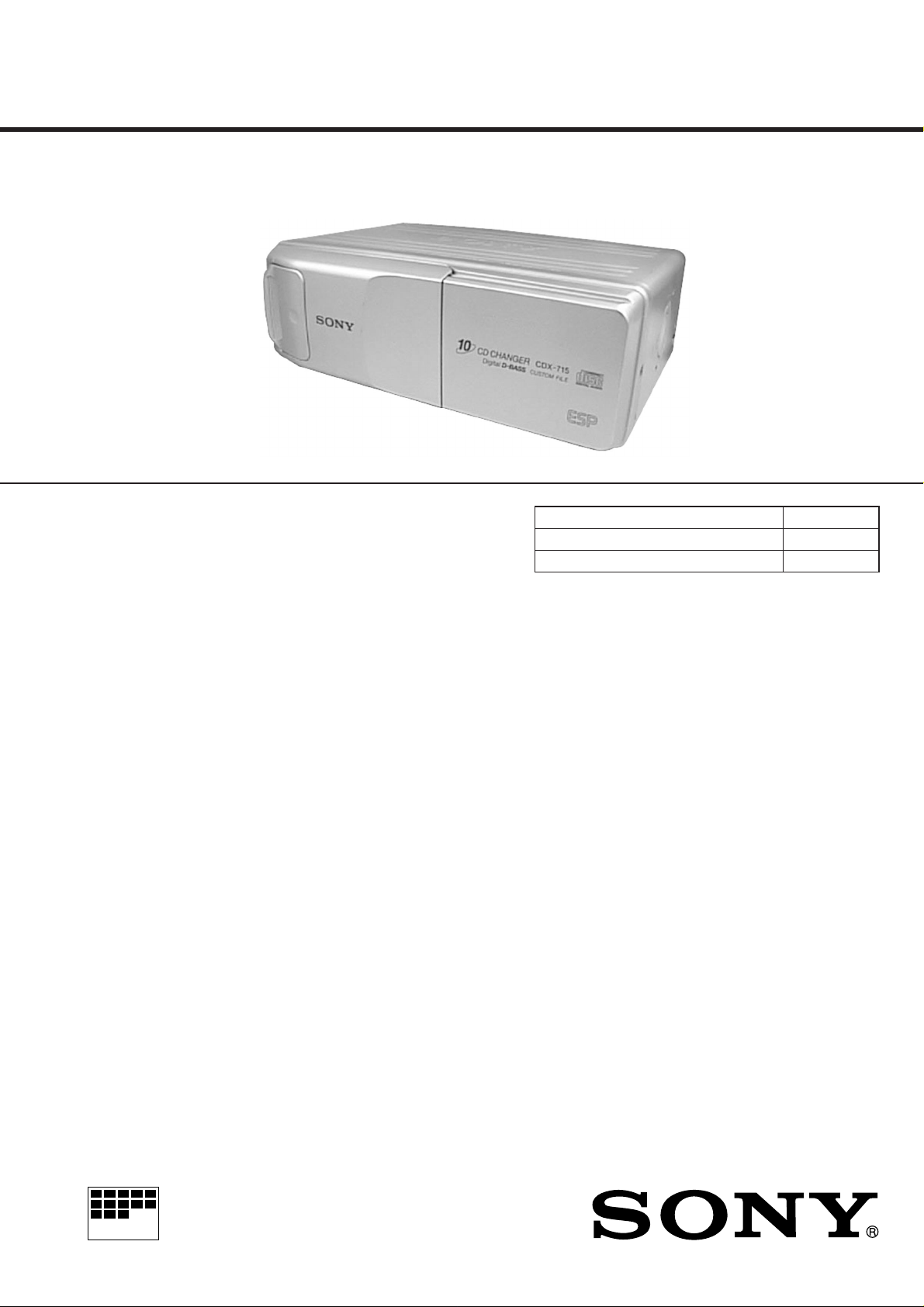
CDX-715
SERVICE MANUAL
SPECIFICATIONS
System Compact disc digital audio system
Laser diode properties Material: GaAlAs
Wavelength: 780 nm
Emission Duration: Continuous
Laser out-put Power: Less than 44.6 µW*
* This output is the value measured at a
distance of 200 mm from the objective lens
surface on the Optical Pick-up Block.
Frequency response 10 – 20,000 Hz
Wow and flutter Below the measurable limit
Signal-to-noise ratio 94 dB
Outputs BUS control output (8 pins)
Analog audio output (RCA pin)
US Model
Canadian Model
AEP Model
UK Model
E Model
Model Name Using Similar Mechanism NEW
CD Drive Mechanism Type MG-250B-137
Optical Pick-up Name KSS-521A/J2N
Currnet drain 800 mA (during CD playback)
800 mA (during loading or ejecting a disc)
Operating temperature –10˚C to +55˚C (14˚F to 131˚F)
Dimensions Approx. 262 × 90 × 181.5 mm
(10 3/8 × 3 5/8 × 7 1/4 in.)
(w/h/d)
not incl. projecting parts and controls
Mass Approx. 2.1 kg (4 lb. 10 oz.)
Power requirement 12 V DC car battery (negative ground)
Supplied accessories Disc magazine (1)
Parts for installation and connections (1 set)
Design and specifications subject to change without notice.
MICROFILM
COMPACT DISC CHANGER
Page 2

SECTION 1
SERVICE NOTE
TABLE OF CONTENTS
1. SERVICE NOTE ........................................................ 2
2. GENERAL
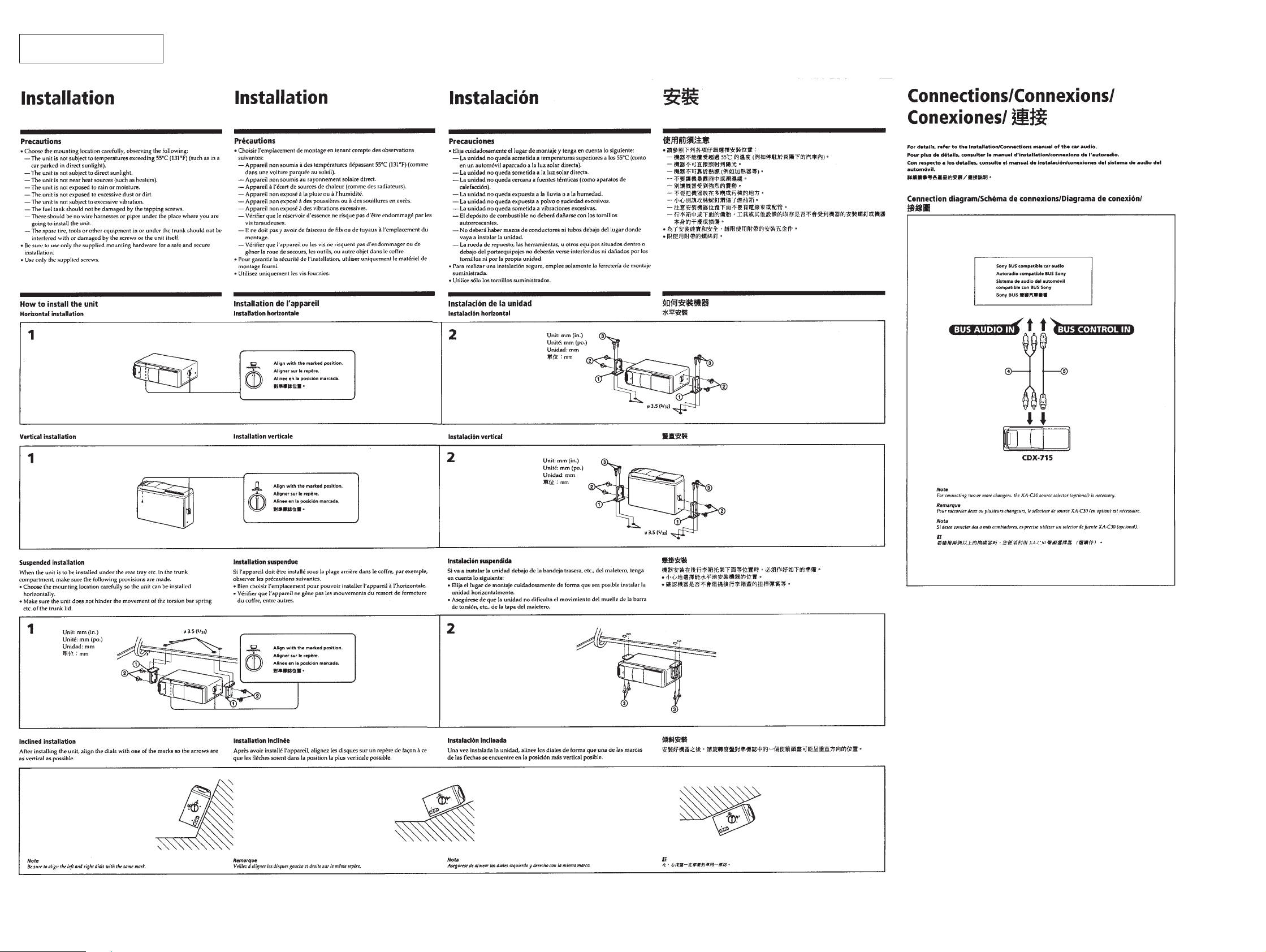
Installation....................................................................... 5
Connections ..................................................................... 6
3. DISASSEMBLY ......................................................... 8
4. MECHANISMDECK ASSEMBLY...................... 14
5. MECHANICAL ADJUSTMENTS....................... 18
6. ELECTRICAL ADJUSTMENTS......................... 19
7. DIAGRAMS
7-1. Block Diagram
– SERVO Section – ......................................................... 21
– MAIN Section – ........................................................... 23
7-2. Printed Wiring Boards – RF Section – .......................... 25
7-3. Schematic Diagram – RF Section –................................ 27
7-4. Printed Wiring Board
– MAIN Section – MAIN Board (Component side) ...... 29
– MAIN Section – MAIN Board (Conductor side)........ 31
7-5. Schematic Diagram
– MAIN Section – MAIN Board (1/2) ........................... 33
– MAIN Section – MAIN Board (2/2) ........................... 35
7-6. Printed Wiring Board – JACK Section –....................... 37
7-7. Schematic Diagram – JACK Section –........................... 38
7-8. IC Pin Function Description ........................................... 45
8. EXPLODED VIEWS ................................................ 47
9. ELECTRICAL PARTS LIST ............................... 52
NOTES ON HANDLING THE OPTICAL PICK-UP
BLOCK OR BASE UNIT
The laser diode in the optical pick-up block may suffer electrostatic breakdown because of the potential difference generated by
the charged electrostatic load, etc. on clothing and the human body .
During repair, pay attention to electrostatic breakdown and also
use the procedure in the printed matter which is included in the
repair parts.
The flexible board is easily damaged and should be handled with
care.
Laser Diode Properites
• Material: GaAlAs
• Wavelength: 780 nm
• Emission Duration: continuous
• Laser Output Power: less than 44.6 µW*
* This output is the value measured at a distance of 200 mm
from the objective lens surface on the Optical Pick-up Block.
CAUTION
Use of controls or adjustments or performance of procedures
other than those specified herein may result in hazardous radiation exposure.
Flexible Circuit Board Repairing
• Keep the temperature of the soldering iron around 270 ˚C during repairing.
• Do not touch the soldering iron on the same conductor of the
circuit board (within 3 times).
• Be careful not to apply force on the conductor when soldering
or unsoldering.
Notes on chip component replacement
• Never reuse a disconnected chip component.
• Notice that the minus side of a tantalum capacitor may be damaged by heat.
– 2 –
SAFETY-RELATED COMPONENT WARNING!!
COMPONENTS IDENTIFIED BY MARK ! OR DOTTED
LINE WITH MARK ! ON THE SCHEMATIC DIAGRAMS
AND IN THE PARTS LIST ARE CRITICAL TO SAFE
OPERATION. REPLACE THESE COMPONENTS WITH
SONY PARTS WHOSE PART NUMBERS APPEAR AS
SHOWN IN THIS MANUAL OR IN SUPPLEMENTS PUBLISHED BY SONY.
ATTENTION AU COMPOSANT AYANT RAPPORT
À LA SÉCURITÉ!
LES COMPOSANTS IDENTIFIÉS P AR UNE MARQUE !
SUR LES DIAGRAMMES SCHÉMATIQUES ET LA LISTE
DES PIÈCES SONT CRITIQUES POUR LA SÉCURITÉ
DE FONCTIONNEMENT. NE REMPLACER CES COMPOSANTS QUE PAR DES PIÈCES SONY DONT LES
NUMÉROS SONT DONNÉS DANS CE MANUEL OU
DANS LES SUPPLÉMENTS PUBLIÉS PAR SONY.
Page 3
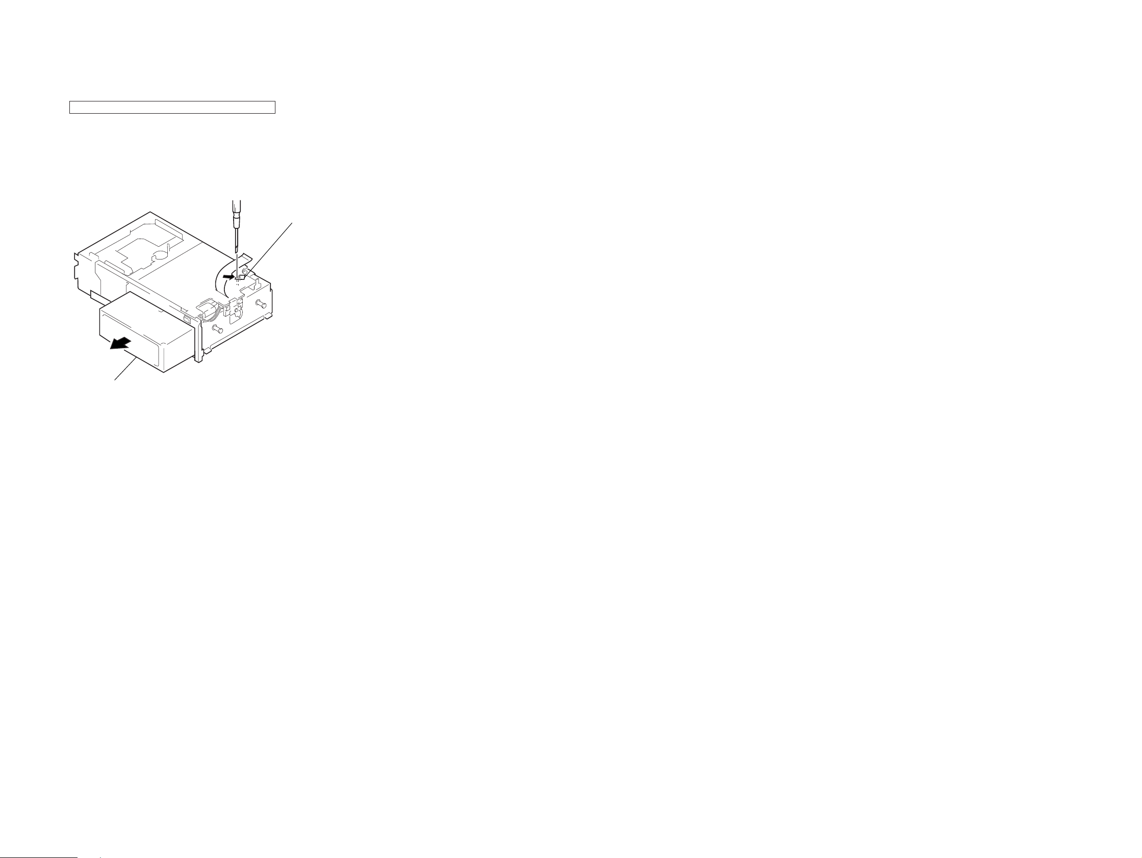
DISC MAGAZINE GETTING OUT PROCEDURE ON
Lever (stop) ass’y
Magazine ass’y
THE POWER SUPPLY IS OFF
Remove the CASE (LOWER) assembly beforehand
1) Press the lever (stop) ass’y to arrow direction.
2) Removal the magazine ass’y.
Note: Take out the magazine only when the tray is completely within the
magazine. If the disc or tray is sticking out, turn on the power and
eject the magazine.
– 3 – – 4 –
Page 4
This section is extracted from
instruction manual.
SECTION 2
GENERAL
– 5 – – 6 –
Page 5
– 7 –
Page 6
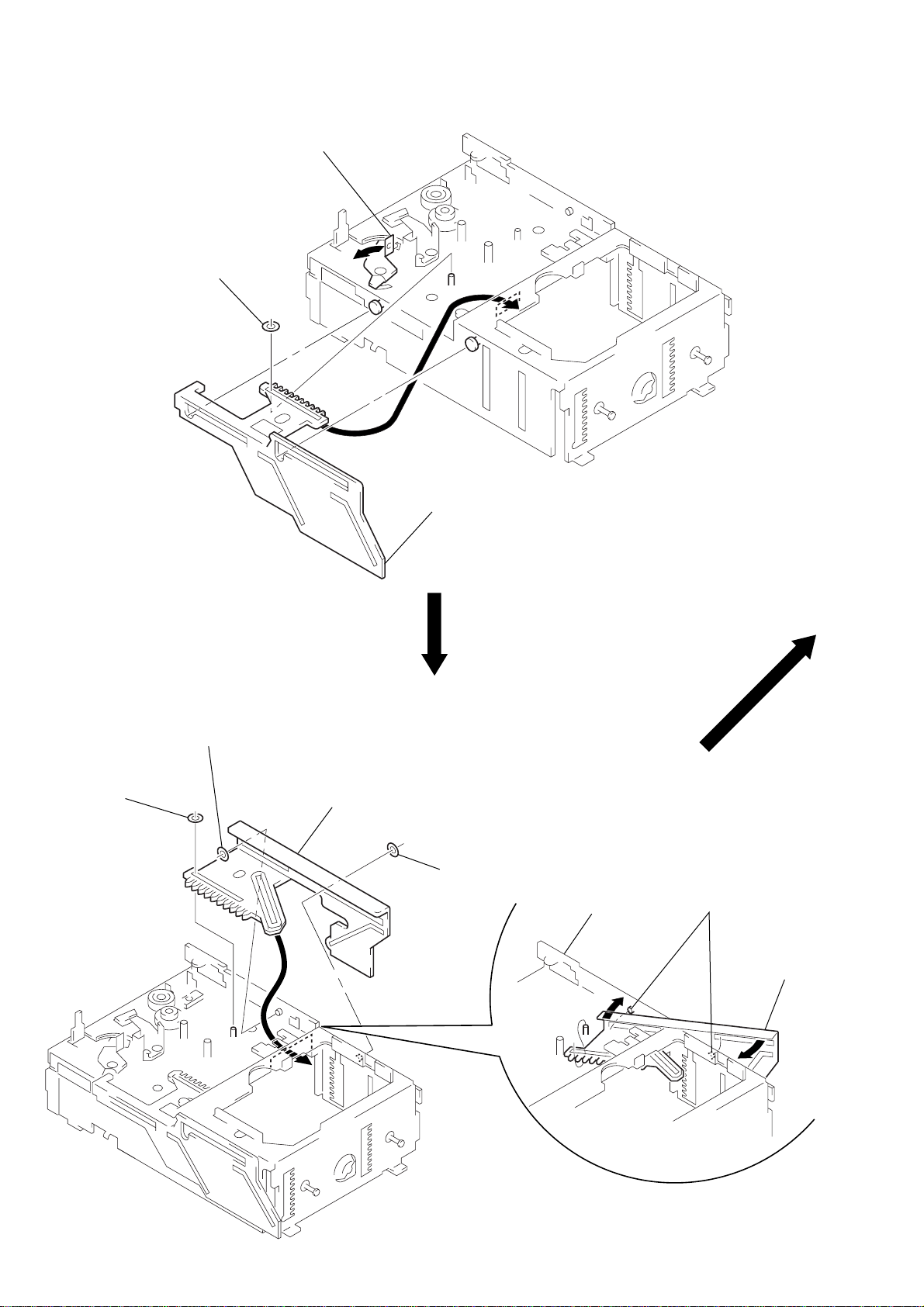
SECTION 3
)
DISASSEMBLY
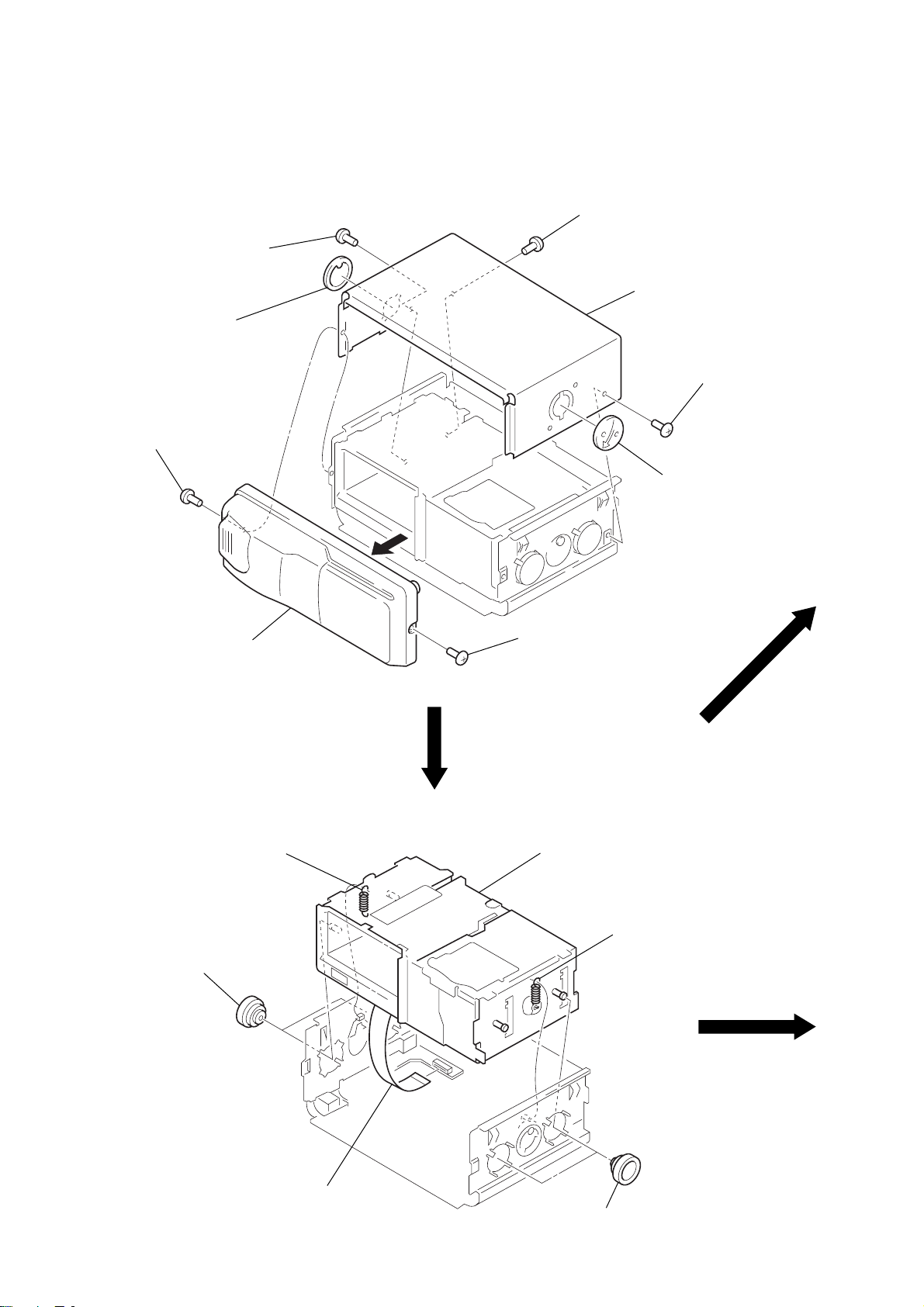
Note: Follow the disassembly procedure in the numerical order given.
COVER (UPPER), FRONT PANEL ASS’Y
1
screw
(PTT2.6 × 6)
3
lever (FL)
1
screw
(PTT2.6 × 6)
1
screw
(PTT2.6 × 6)
2
case (upper)
3
1
screw
(PTT2.6 × 6)
lever (FL)
4
front panel ass’y
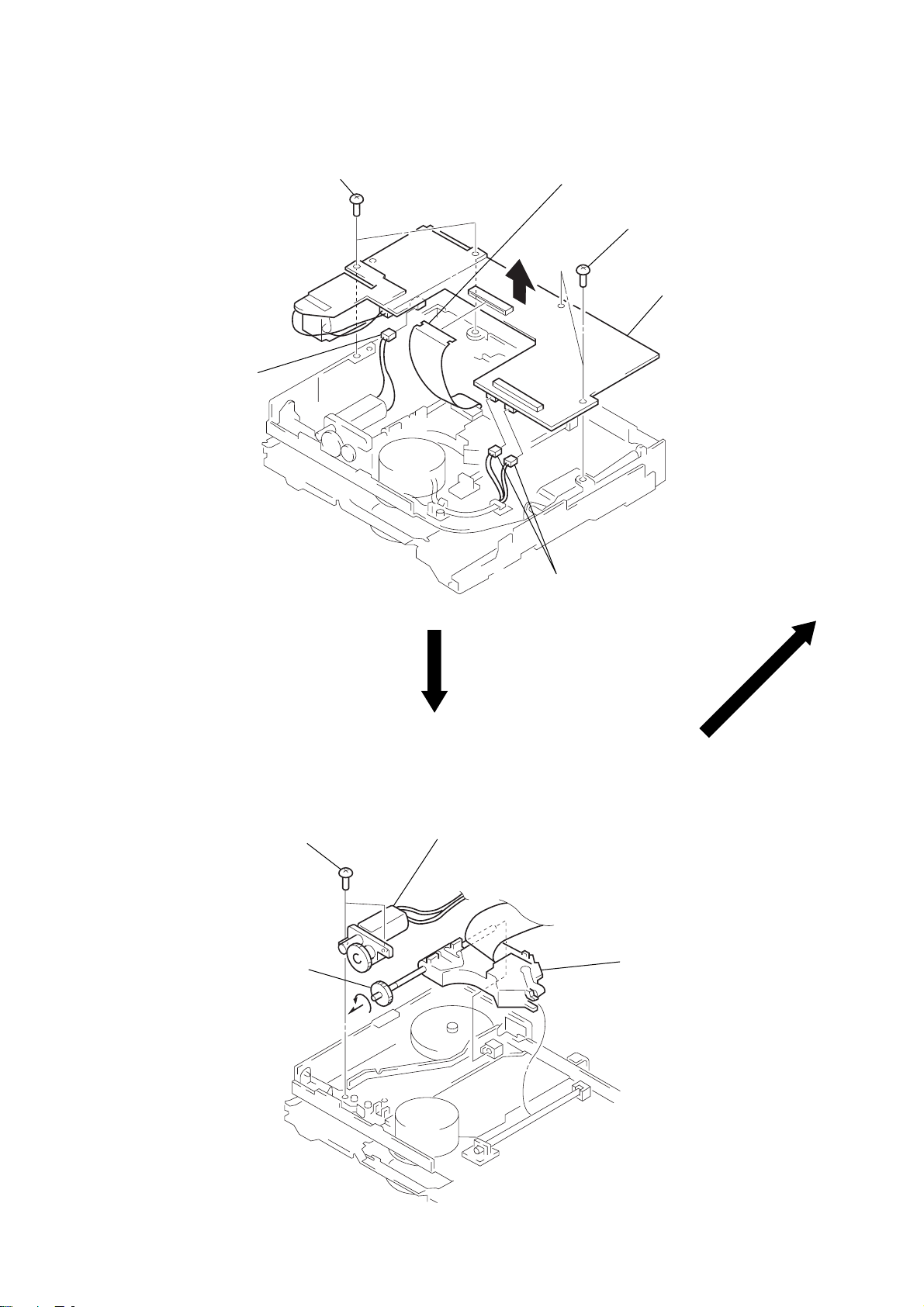
MECHANISM DECK (MG-250B-137)
2
spring (FL)
1
two dampers (250)
1
screw
(PTT2.6 × 6)
4
mechanism deck (MG-250B-137
2
spring (FL)
3
jack flexible board
(CN901)
– 8 –
1
two dampers (250)
Page 7
JACK BOARD
Remove the JACK board of
the arrow.
1
ground point screw
(+PTT2.6 × 6)
2
JACK board
MAIN BOARD
5
screw
(P1.4
×
3.0)
1
main flexible board
(CNJ12)
6
three screws
7
MAIN board
2
connector
(CNP301)
3
screw
(BVTT2
×
4)
5
screw
(P1.7
×
2.5)
– 9 –
4
heat sink
Page 8
ELEVATOR MOTOR ASS’Y (M104)
1
screw
(P2 × 2.2)
2
bracket (ELV motor)
3
elevator motor ass’y
ESCUTCHEON
2
Remove the claw
of the arrow
4
Remove the ditch
of the arrow
5
Remove the escutcheon
of the arrow
A
B
C
3
two claws
.
A
.
.
B
4
C
ditch
1
screw
(M2
– 10 –
×
3)
Page 9
CASE (UPPER) ASS’Y
4
three screws
(B2 × 3)
7
Remove the case
(upper) ass’y of
the arrow B.
4
screw
(B2 × 3)
3
spring (stopper. upper)
4
two screws
(B2 × 3)
6
Remove the edge
of the arrow A.
2
bracket (stopper upper)
1
screw
(P2 × 2.2)
5
A
B
r
CHASSIS ASS’Y
5
chassis ass’y
4
4
3
polyethylene washe
1
stop ring 2.0
(E type)
2
washer
– 11 –
6
spring (stopper. lower)
Page 10
RF BOARD
)
5
connector
(CNP52)
2
two screws
(PS2
1
×
4)
OP flexible board
(CNJ11)
3
two screws
(PS2
×
4)
4
RF board
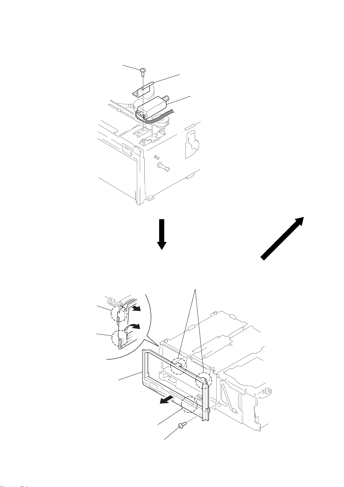
SLED MOTOR ASS’Y (M102), OPTICAL PICK-UP (KSS-512A/J2N)
1
4
Turn at the direction of the
arrow, then remove
shaft (sled) ass’y
two screws
(P2 × 3)
2
sled motor ass’y
(M102)
5
two connectors
(CNP11, 503)
3
optical pick-up
(KSS-521A/J2N
– 12 –
Page 11
SW BOARD, SPINDLE MOTOR ASS’Y (M101)
8
two screws
(P1.7
×
2.2)
1
screw
×
2.2)
(P2
2
SW board
7
3
spring (chucking)
6
retainer (disc)
4
screw
×
(P2
5
bracket (CP)
9
Remove the spindle motor ass’y (M101)
of the arrow.
2.2)
CHUCKING MOTOR ASS’Y (M103)
3
bracket
(load motor)
2
two screws (P2 × 2.5)
1
connector
(CNP51)
4
chucking motor ass’y
(M103)
– 13 –
Page 12
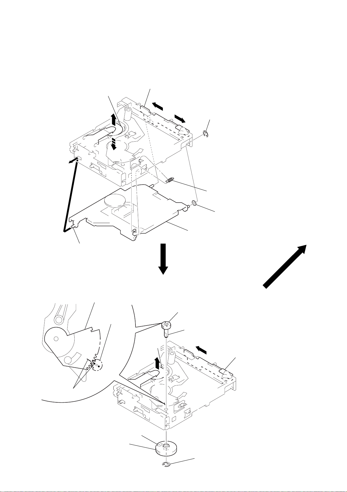
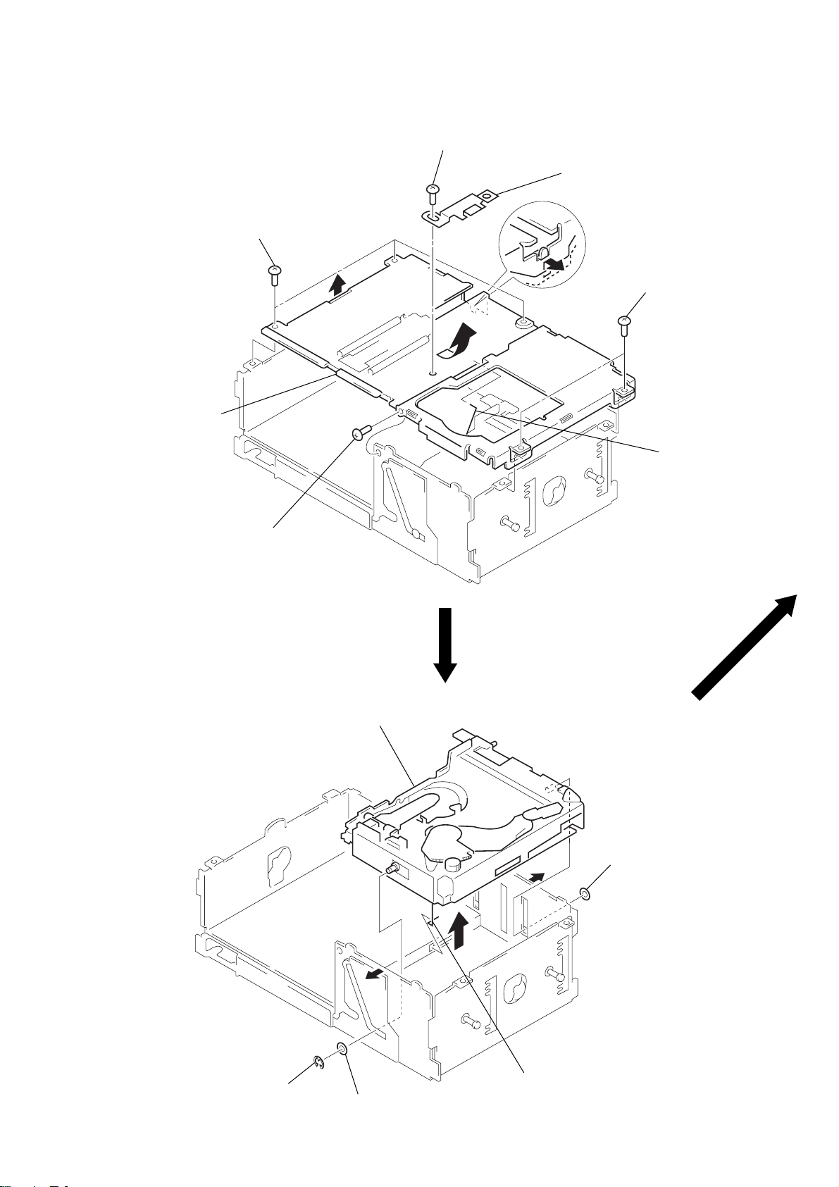
SECTION 4
MECHANISMDECK ASSEMBLY
Note: Follow the assembly procedure in the numerical order given.
OPTICAL PICK-UP COMPLETE ASS’Y
1
Move the lever (LOCK 3) in direction A, and return it a little in
direction
to the lower limit.
chuck plate
B
from the position where the chuck plate is moved down
B
shaft (A)
A
3
4
stop ring 2.0 (E type)
5
tension spring (DH)
2
polyethylene washer
optical pick-up complete ass’y
Note: Insert the shaft (A) first.
GEAR (LOMINI) / (LOAD 1) ASS’Y
gear (LOAD 2)
gear (LOMINI)
marking
Fig. A.
3
Attach the gear (LOAD 1) ass’y
with its facing inside.
chuck plate
slit
2
Attach the gear (LOMINI) at the position
shown in Fig. A.
shaft (rotary prevention C)
1
B
4
stop ring 1.5 (E type)
Move the lever (LOCK 3)
fully in direction B to
move the chuck plate up.
– 14 –
Page 13
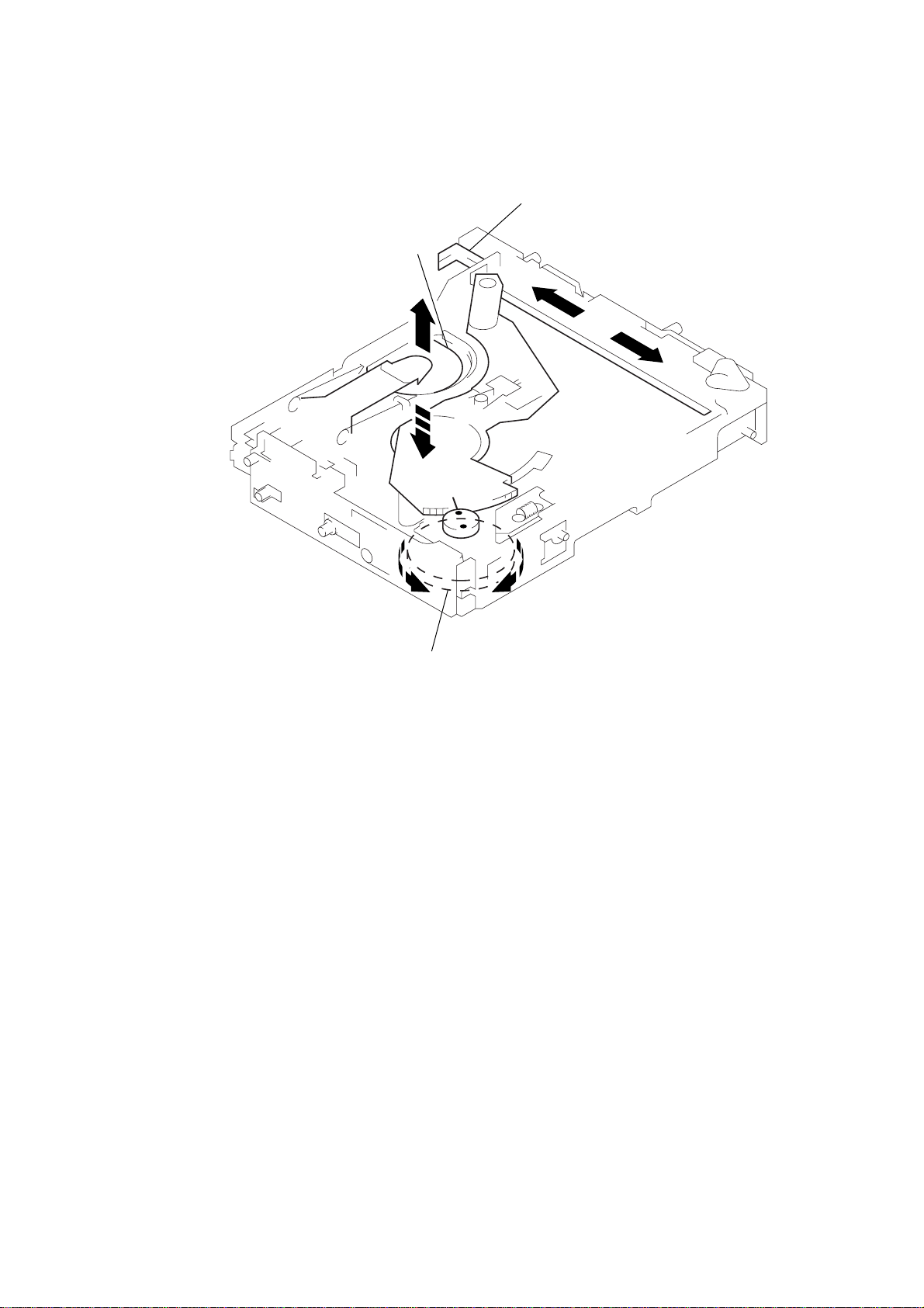
OPERATION CHECK
1
Confirm that the slider moves in direction C to move down the
chuck plate if the gear (LOAD 1) is rotated in direction A or the
chuck plate moves up and the slider mo ves in direction D if the
gear is rotated in direction B.
chuck plate
slider
D
C
A
gear (LOAD 1) ass’y
B
– 15 –
Page 14
SLIDER (L)
1
Move the lever (STOP) ass’y in direction
until it gets stopped.
3
washer
A
2
slider (L)
SLIDER (R)
3
washer
4
polyethyelene slider
1
slider (R)
5
polyethyelene washer
case (lower) ass’y
2
Engage the slots of slider (R)
with the shafts.
slider (R)
– 16 –
Page 15

ADJUSTING PHASE OF SLIDERS (L, R)
y
1
Sliding the sliders (L, R) in the arrow direction, meet holes
and b of the sliders (L, R) with holes c and d of the case
(LOWER) ass’y
a
a
b
slider (R)
d
GEAR (ELV2) / (ELV3)
3
5
tension spring
(STOP LEVER)
c
4
retaining ring
gear (ELV 2)
slider (L)
case (LOWER) ass’
2
retaining ring
1
gear (ELV 3)
Note:After mounting the gear, confirm
that the holes for phase adjustment
are not shifted.
– 17 –
Page 16

MECHANICAL ADJUSTMENTS
5
• Elevator Height (Address) Adjustment
SECTION 5
Note: This adjustments is necessary when the system controller (IC201),
variable resistor (RV201), slider (R), slider (L), or chassis (ELV)
was replaced for any repair.
Connection:
power supply
master unit
+
GND
BUS cable
CDX-715
Adjustment Method:
1. Connect this set to the master unit (e.g. MDX-C670/
C670RDS), load a disc magazine, and place the set vertically
as shown below.
2. Connect the regulated power supply to the master unit, and
turn the power on.
3. Press the DISC button on the master unit and select DISC 5.
4. At this time, if the elevator shaft does not position between
comb teeth A and B at addresses 5 and 6 as shown below,
adjust the following.
5. Press repeatedly the DISC + and – buttons on the master unit
so that the elevator shafts moves from address 6 to address 5,
or from 5 to 6. At this time, adjust RV201 on the main board
so that the elevator shaft positions smoothly between comb
teeth A and B.
6. Further, place the set horizontally and make same adjustment
as mentioned above.
7. After adjustment at addresses 5 to 6 is finished, check all op-
erations from addresses 1 to 10 with the set placed vertically
and horizontally respectively to confirm that the ele v ator shaft
positions in a range between comb teeth A to B.
comb tooth at address 5
comb tooth at address 6
A
B
comb tooth at address 6
elevator shaft
A
B
OK NG
elevator shaft
comb tooth at address
RV201
– 18 –
Page 17

SECTION 6
MIN side
(low gain)
MAX side
(high gain)
RV14 standard position
ELECTRICAL ADJUSTMENTS
Note:
1. Perform adjustments as given.
2. Be sure to use the disc “YEDS-18” parts code: 3-702-101-01, but
only when indicated.
3. Power supply voltage: DC14.4 V (more than 3A).
• FOCUS BIAS CHECK
[RF BOARD] – Conductor Side –
oscilloscope
CNJ12
TP (RF)
IC51
TP
(VC)
IC11
+
–
Procedure:
1. Connect the oscilloscope to RF board test point RF.
2. Put the set into play mode by loading the disc.
3. Confirm that oscilloscope waveform is clear and check RF signal level is correct or not.
Note:
Clear RF signal waveform means that the shape “≈” can be clearly distinguished at the center of the waveform.
RF signal waveform
VOLT/DIV: 200 mV
TIME/DIV: 500 nsec
• TRACKING OFFSET CHECK
[RF BOARD] – Conductor Side –
oscilloscope
CNJ12
+
–
BP11
IC51
(TE)
TP
(VC)
IC11
Procedure:
1. Connect the oscilloscope to RF board bridge point TE.
2. Put the set into play mode by loading the disc.
3. Press the = AMS + button, then, c heck the traverse wa veform.
4. Confirm that the oscilloscope waveform is symmetrical on the
top and bottom in relation to 0 V dc, and check this level.
* Traverse waveform: This is the tracking error wave form
appears when crossing the track.
VOLT/DIV : 500 mV
TIME/DIV : 2 msec
Center : 0 V
A
0 V
B
• FOCUS GAIN ADJUSTMENT
(COARSE ADJUSTMENT)
This adjustment is to be performed when replacing the following
parts.
• Optical Pick-up Block
• RV14
[RF BOARD] – Conductor Side –
CNJ12
IC51
RV14
IC11
Procedure:
1. Set RV14 (RF board) to the standard position.
2. Check that there is not an abnormal amount of operation noise
(white noise) from the 2-axis devise. If there is, turn RV14
slightly clockwise.
[RF BOARD] – Conductor Side –
• When gain is lowered...
The set does not play because of no focus operation.
• When gain is highered...
Operation noise is heard due to a scratch or a dust, then operation will be unstable.
level: 1.4 ± 0.3 Vp-p
A=B
traverse waveform
(100 track jump waveform)
– 19 – – 20 –
Page 18

CDX-715
7-1. BLOCK DIAGRAM – SERVO Section –
SECTION 7
DIAGRAMS
DETECTOR
ABD
C
F
E
OPTICAL PICK-UP
(KSS-521A)
LASER DIODE
PD
I-V AMP
LD
PD1 I-V AMP
PD1
38
PD2 I-V AMP
PD2
39
AUTOMATIC
POWER CONTROL
Q11
F
41
E
42
LD
36
RF
+
SUMMING
AMP
RF AMP,
FOCUS/TRACKING
SERVO
IC11 (1/2)
I-V
AMP
LD
AMPPDAMP
FOCUS
ERROR
AMP
TRACKING
ERROR
AMP
PD
37
RFO
33
RFI
32
FOCUS OK
COMPARATOR
MIRR
AMP
DEFECT
AMP
FEO
FE BIAS
TEO
DIGITAL SIGNAL PROCESSOR,
CLV SERVO
IC101
RF
ASYI
ASYO
FOK
DATO
CLKO
XLTO
SEIN
CNIN
IC201 (1/2)
ASYMMETRY
CORRECTION
CD.DATA
SERVO AUTO SEQUENCER
DIGITAL CLV
MON
26
52
SUBQ
51
SCLK
23
SENS
67
65
CD.CLK
66
CD.XLT
63
SCOR
24
GFS
44
46
47
FOK
DATA
CLK
XLT
LOCK
XRST
SENS1
C.OUT
SENS2
FEO
TAO
27
22
20
21
19
23
25
24
26
6
13
FOCUS OK
AMP
TTL
IIL
1
RV14
FOCUS
40
GAIN
45
FEI
2
TEI
47
TTL
IIL
IIL
IIL DATA REGISTER
TTL
FOCUS PHASE
COMPENSATION
TRACKING PHASE
COMPENSATION
23
15
17
16
13
14
SYSTEM CONTROLLER
C.OUT
54
FOK
22
SENS2
8
FILTER
39
42
FILO
CLTV
DIGITAL PLL
XROF
MDS29LOCK64SQSO
MDP
28
27
PCO
4038
FILI
SQCK
8 7
EFM
DEMODULATOR
SUB-CODE
PROCESSOR
CPU INTERFACE
SENS
XLAT
CLOCK
DATA
91012
117576
SCOR
SBSO
EXCK
77
INTERNAL BUS
GFS
XRST
100
89
61
D/A
16K
RAM
ERROR
CORRECTOR
CLOCK
GENERATOR
XTAI
EDGE DETECT
PCMD
BCKO
LRCK
C2PO
INTERFACE
RFCK
WDCK
GTOP
WFCK
EMPH
IC403 (1/2)
C4M
52
54
50
63
62
49
IC403 (2/2)
2
1
58
74
72
70
DATI
11
9
BCKI
LRCI
12
7
RFCK
7
WDCI
13
8
GTOP
3
WFCK
5
C4M
6
XROI
D-RAM
CONTROLLER
IC401
47
SDTI
48
SCK
61
SCOR
DATA
BCK
LRCK
XTAI
18
17
19
16
C4M
A
(Page 23)
B
(Page 23)
21
FOCUS/TRACKING COIL DRIVE,
SPINDLE/SLED MOTOR DRIVE
2-AXIS
DEVICE
(FOCUS)
(TRACKING)
05
M102
M
(SLED)
M101
(SPINDLE)
M
OUT+
2
OUT–
1
OUT+
12
OUT–
13
OUT+
26
OUT–
27
OUT+
17
OUT–
16
IC51
TRACKING
COIL DRIVE
FOCUS
COIL DRIVE
SLED
MOTOR DRIVE
SPINDLE
MOTOR DRIVE
IN
4
IN
10
SLED SERVO
IC11 (2/2)
IN
24
IN
19
SLO
16 14
SLED
AMP
(CHUCKING)
M103
SLP
M
CHUCKING MOTOR DRIVE
IC52
OUT1
1
7
OUT2
CHUCKING
MOTOR DRIVE
RIN
FIN
4
5
CH.F
4
CH.R
5
XRST
GRSRT
GRSCOR
XQOK
SDTI
XSOE
ESPXLT
XRDE
XWRE
LOAD1
LOAD2
LIM.SW 9
25
46
26
27
28
29
41
42
SW12
(SAVE END DETECT)
7
SW11
(CHUCKING END DETECT)
6
SW1
(LIMIT)
GRSRT
1
60
XRDE
SDTO
GSCR
59
XLT
XQOK
XSOE
50
494645
ON : When completion of the disc
chucking operation.
ON : When completion of the disc
chucking operation.
ON : When the optical pick-up
is inner position.
44
XWRE
A0 – A9
25 – 22, 40 – 36, 27
9 – 12, 14 – 18, 5
A0 – A9
D1 – D4
31, 30, 33, 32
1, 2, 24, 25
D1 – D4
D-RAM
IC402
XRAS
XCAS
342835
23422
XCAS
XRAS
XOE
XWE
29
3
XOE
XWE
• SIGNAL PATH
XRST
: CD PLAY
C
(Page 23)
– 21 – – 22 –
Page 19

CDX-715
– MAIN Section –
A
(Page 22)
XRST
C
(Page 22)
C4M
B
(Page 22)
DIGITAL FILTER,
XO
HS
21
LINEAR POSITION
D/A CONVERTER,
LOW-PASS FILTER
IC601
DIGITAL FILTER
CIRCUIT
MICRO COMPUTER
INTERFACE
CIRCUIT
EMP
19
RV201
SENSOR
LOW-PASS
FILTER
CIRCUIT
LOW-PASS
FILTER
CIRCUIT
LO
9
RO
5
MUTING
CONTROL SWITCH
Q601, 602
MUTING
Q610
MUTING
Q620
CN901 (1/2)
AUDIO OUT L
AUDIO OUT R
• SIGNAL PATH
: CD PLAY
COMPRESSOR
IC102
DATAI
3
BCKI
2
LRCKI
1
RST
6
INPUT
INTERFACE
CIRCUIT
SEQUENTIAL
CONTROL
DIGITAL
SIGNAL
PROCESSOR
MODE
CONTROL
MODE2
MODE1
14
15
16
MODE3
OUTPUT
INTERFACE
CIRCUIT
SYSTEM
CLOCK
75
74
SYSTEM CONTROLLER
MODE2
MODE1
DATAO
BCKO
LRCKO
CLK
IC201 (2/2)
9
10
11
4
ML
EMP
A.MUTE
MCK
DATA
22
BCK
LRCK
MCK
45
44
43
38
INTERFACE
CIRCUIT
TIMING
GENERATOR
OSC
XI
15
16
X601
16.9344MHz
23
24
13
M104
(ELEVATOR)
EHS
AVREF
ELV.ON
CD.ON
BU.CHK
SCK
BUS.ON
RST
W.UP
39
37
69
68
61
SI
49
SO
50
48
55
30
D306
62
SW201
MAGAZINE EJECT
END DETECT
SW202
MAGAZINE IN/OUT
DETECT
ELEVATOR MOTOR DRIVE
IC301
EEPROM
IC202
FIN
RIN
SDA
SCL
4
5
5
6
OUT1
1
M
7
OUT2
ELEVATOR
MOTOR DRIVE
57
60
70
58
12
11
MGLK
MAG.SW
ELV.R
ELV.F
EE.DATA
EE.CLK
RV202
ELEVATOR HEIGHT
SENSOR
REFERENCE VOLTAGE
SWITCH
Q201
MICON +5V
BUS INTERFACE
(FOR SONY BUS)
IC302
SO
10
SI
9
SCK
11
BUSON OUT
1
BUSON OUT
13
RESET
8
RESET SIGNAL
GENERATOR
IC304
RESET
SWITCH
DATA
CLK
LOF
BUSON IN
RST
MICON +5V
+9V
MICON +5V
DAC +5V,
SERVO +5V
6
4
12
2
7
D311
+5V
REGULATOR
IC305
BATTERY
CHECK
Q301, 302
+9V
REGULATOR
IC303
REGULATOR
Q303
B+ SWITCH
Q304, 305
LEVEL SHIFT
D307
D309
D313
D308
BUS CONTROL CONNECTOR
(FOR SONY BUS)
7
5
4
6
2
CN901 (2/2)
B.UP
DATA
CLK
BUSON
RST
EJECT
05
XTAL
X201
8MHz
EXTAL
3132
64
SW301
6
MICON +5V
– 23 – – 24 –
Page 20

CDX-715
• Semiconductor
Location
Ref. No. Location
IC11 C-6 IC51 B-7 IC52 G-4
Q11 D-6
Note on Printed Wiring Boards:
• Y : parts extracted from the conductor side.
r
•
• b : Pattern from the side which enables seeing.
(The other layers' patterns are not indicated.)
Caution:
Pattern face side: Parts on the pattern face side seen from
(Conductor Side) the pattern face are indicated.
Parts face side: Parts on the parts face side seen from
(Component Side) the parts face are indicated.
: Through hole.
7-2. PRINTED WIRING BOARDS – RF Section –
Note on Schematic Diagram:
• All capacitors are in µF unless otherwise noted. pF: µµF
50 WV or less are not indicated except for electrolytics
and tantalums.
• All resistors are in Ω and 1/
specified.
Note:
The components identified by mark ! or dotted
line with mark ! are critical for safety.
Replace only with part
number specified.
• U : B+ Line.
• H : adjustment for repair.
• Power voltage is dc 14.4 V and fed with regulated dc power
supply from CD changer controller.
• Voltages and waveforms are dc with respect to ground
under no-signal conditions.
no mark : PLAY
• Voltages are taken with a VOM (Input impedance 10 MΩ).
Voltage variations may be noted due to normal production tolerances.
• Waveforms are taken with a oscilloscope.
Voltage variations may be noted due to normal production tolerances.
• Circled numbers refer to waveforms.
• Signal path.
J : CD
4
W or less unless otherwise
Note:
Les composants identifiés par
une marque ! sont critiques
pour la sécurité.
Ne les remplacer que par une
piéce portant le numéro
spécifié.
– 25 – – 26 –
Page 21

7-3. SCHEMATIC DIAGRAM – RF Section – • See page 25 for Note on Schematic Diagram. • See page 39 for Waveforms. • See page 41 and 42 for IC Block Diagrams.
CDX-715
– 27 – – 28 –
Page 22

CDX-715
• Semiconductor
Location
(Component Side)
Ref. No. Location
D301 F-4 D302 F-4 D303 F-4 D304 E-2 D305 E-2 D306 E-6 D307 G-4 D308 F-4 D309 E-2 D310 E-3 D311 F-5 D312 E-3 D313 C-2 D314 F-3
IC101 B-6 IC102 D-5 IC201 E-7 IC202 D-8 IC301 F-3 IC302 F-5 IC304 G-4 IC401 B-5 IC402 C-5 IC403 B-4 IC601 E-5
7-4. PRINTED WIRING BOARD – MAIN Section – MAIN Board (Component Side)
• See page 32 for Note on Printed Wiring Board. • See page 33 to 36 for Schematic Diagram.
Q201 E-8 Q301 G-4 Q302 G-4 Q303 F-4 Q304 B-2 Q601 C-3 Q602 C-3 Q610 D-3 Q620 C-3
– 29 – – 30 –
Page 23

– MAIN Section – MAIN Board (Conductor Side)
• See page 33 to 36 for Schematic Diagram.
CDX-715
• Semiconductor
Location
(Conductor Side)
Ref. No. Location
IC303 E-8 IC305 D-8
Q305 C-8
Note on Printed Wiring Board:
• X : parts extracted from the component side.
• Y : parts extracted from the conductor side.
r
•
•
• b : Pattern from the side which enables seeing.
(The other layers' patterns are not indicated.)
: Through hole.
¢
: internal component.
Caution:
Pattern face side: Parts on the pattern face side seen from
(Conductor Side) the pattern face are indicated.
Parts face side: Parts on the parts face side seen from
(Component Side) the parts face are indicated.
– 31 – – 32 –
Page 24

CDX-715
7-5. SCHEMATIC DIAGRAM – MAIN Section – MAIN Board (1/2)
• See page 39 and 40 for Waveforms. • See page 42 to 44 for IC Block Diagrams. • See page 45 and 46 for IC Pin Function Description. • See page 36 for Note on Schematic Diagram. • See page 29 to 32 for Printed Wiring Board.
– 33 – – 34 –
Page 25

– MAIN Section – MAIN Board (2/2)
• See page 40 for Waveforms. • See page 43 and 44 for IC Block Diagrams. • See page 29 to 32 for Printed Wiring Board.
CDX-715
Note on Schematic Diagram:
• All capacitors are in µF unless otherwise noted. pF: µµF
50 WV or less are not indicated except for electrolytics
and tantalums.
• All resistors are in Ω and 1/
specified.
¢
•
• U : B+ Line.
• H : adjustment for repair.
• Power voltage is dc 14.4 V and fed with regulated dc power
• Voltages and waveforms are dc with respect to ground
• Voltages are taken with a VOM (Input impedance 10 MΩ).
• Waveforms are taken with a oscilloscope.
• Circled numbers refer to waveforms.
• Signal path.
: internal component.
supply from CD changer controller.
under no-signal conditions.
no mark : PLAY
Voltage variations may be noted due to normal production tolerances.
Voltage variations may be noted due to normal production tolerances.
J : CD
: Impossible to measure
∗
4
W or less unless otherwise
– 35 – – 36 –
Page 26

CDX-715
7-6. PRINTED WIRING BOARD – JACK Section – 7-7. SCHEMATIC DIAGRAM – JACK Section –
Note on Schematic Diagram:
• All capacitors are in µF unless otherwise noted. pF: µµF
50 WV or less are not indicated except for electrolytics
and tantalums.
• All resistors are in Ω and 1/
specified.
• C : panel designation.
• U : B+ Line.
• Signal path.
J : CD
• Abbreviation
G : German model.
4
W or less unless otherwise
Note on Printed Wiring Board:
• X : parts extracted from the component side.
• p : parts mounted on the conductor side.
r
•
• b : Pattern from the side which enables seeing.
(The other layers' patterns are not indicated.)
Caution:
Pattern face side: Parts on the pattern face side seen from
(Conductor Side) the pattern face are indicated.
Parts face side: Parts on the parts face side seen from
(Component Side) the parts face are indicated.
• Abbreviation
: Through hole.
G : German model.
– 37 – – 38 –
Page 27

• Wavef orms
6 Vp-p
472 ns
– RF Board –
1 IC11 1 (FEO)
500 mV/DIV, 500 nsec/DIV
2 IC11 2 (FEI)
50 mV/DIV, 1 µsec/DIV
1.4 ±0.3 Vp-p
– MAIN Board (1/2) –
1 IC101 @¶ MDP
3.8
2 IC101 $ª WDCK
2.5 Vp-p
µ
s
3 IC11 $¶ (TEI)
200 mV/DIV, 500 µsec/DIV
Approx. 110 mVp-p
Approx. 280 mVp-p
5 Vp-p
11.4 µs
3 IC101 %º LRCK
5 Vp-p
22.5 µs
4 IC101 %¢ BCKO
5 IC101 ^™ RFCK
5 Vp-p
136.5 µs
– 39 –
Page 28

6 IC101 &¢ WFCK
!¡ IC102 0 BCKO
137 µs
7 IC101 *ª XTAI
59 ns
8 IC201 #¡ EXTAL
5 Vp-p
4.5 Vp-p
3.3 Vp-p
5.3 Vp-p
472 ns
!™ IC102 !¡ LRCKO
5.3 Vp-p
22.6 µs
– MAIN Board (2/2) –
!£ IC601 !∞ XI
124.5 ns
9 IC401 !¶ BCK
472 ns
0 IC401 !ª LRCK
2.9 Vp-p
59 ns
5.9 Vp-p
5.8 Vp-p
22.8 µs
– 40 –
Page 29

• IC Block Diagrams
IC11 CXA1992BR (RF BOARD)
FE_BIAS
LPFI
ATSC
TDFCT
VEE
TEO
TZC
FZC
PD2
PD1
RF_O
PD
LD
RFTC
RF_M
RF_I
CP
CB
CC1
CC2
FOK
27282930313233343536373839
VEE
+
–
+
–
–
+
RF SUMMING
AMP
FOH
FOL
TGH
TGL
BALH
BALL
ATSC
TZC
FZC
+
–
–
+
–
+
–
–
+
VEE
MIRR
VCC
–
+
–
–
+
+
–
–
+
VEE
LEVEL S
VCC
–
+
FOK
LDON
LPCL
LPC
TGFL
IIL DATA REGISTER
INPUT SHIFT REGISTER
ADDRESS DECODER
SENS SELECTOR
OUTPUT DECODER
DFCTO
IFB1-6
FS1-4 TG1-2 TM1-7 PS1-4
BAL1-4
TOG1-4
+
SENS2
26
+
–
IIL
↓
VCC
–
+
–
VEE
+
–
+
TTL
DFCT
+
IIL
↓
MIRR
TTL
DFCT1
CC1
TTL
↓
IIL
VCC
ISET
VCC VCC
SENS1
25
C. OUT
24
XRST
23
DATA
22
XLT
21
CLK
20
LOCK
19
VCC
18
ISET
17
SL_O
16
TM4 TM6
SL_M
VCC
FS1
FS2
Charge
up
TG2
TM7
FSET
TM3
TM5
VEEVEE
–
+
15
–
SL_P
14
+
TM2
–
+
PD2 IV
AMP
40
F
41
E
42
–
+
–
+
F IV AMP
PD1 IV
AMP
–
+
VCC
APC
+
–
–
+
+
–
VEE
LASER POWER CONTROL
VCC
FE AMP
–
+
E IV AMP
+
43
EI
BAL1
BAL2
BAL3
BAL4
VEE
44
TOG4
TOG3
TOG2
TOG1
TGFL
–
+
45
+
–
E-F BALANCE
VCC
VEE
WINDOW COMP.
+
–
DFCT
TM1
–
+
–
+
+
–
ATSC
WINDOW
COMP.
–
+
46
47
TEI
48
49
TZC COMP.
50
51
VC
+
–
VCC
52
+
–
IFB4
IFB2
IFB3
IFB1
VEE
+
–
+
TRK. GAIN
–
WINDOW COMP.
+
–
TG1
–
IFB5
IFB6
FOCUS
PHASE COMPENSATION
FO. BIAS
WINDOW
COMP.
TRACKING
PHASE COMPENSATION
DFCT
FZC COMP.
FS4
VEE
1
2 3
FEO
FEI
4
FDFCT
5 6 7 8 9 10
FGD
FLB
FE_O
FE_M
SRCH
TGU
TG2
FSET
TA_M
131211
TA_O
– 41 –
Page 30

IC52, 301 BA6287F (RF BOARD, MAIN BOARD)
1
OUT1
VCC
VM
FIN
2
DRIVER DRIVER
TSD
3
POWER
SAVE
4
CONTROL LOGIC
8
GND
7
OUT2
6
VREF
5
RIN
IC101 CXD2530Q (MAIN BOARD)
TES6
VDD
VSS
EXCK
SBSO
SCOR
WFCK
TES5
EMPH
DOUT
C4M
FSTT
XTSL
MNT0
MNT1
66 65 64
67
ERROR
CORRECTOR
16K RAM
SERVO
AUTO
MNT3
VSS
VDD
TES7
VSS
XVDD
XTAI
XTAO
XVSS
VSS
TES8
VDD
VSS
XRST
79 78
80
NC
81
82
83
NC
84
85
86
NC
87
88
89
90
91
92
NC
93
94
NC
95
96
97
98
NC
NC
99
100
TIMING
LOGIC
76 75 74
77
73 72
DEMODULATOR
SUB CODE
PROCESSOR
CPU
INTERFACE
EFM
69 68
70
71
SEQUENCER
XROF
C2PO
63 62 61
RFCK
GFS
XPCK
59 58
60
D / A
INTERFACE
DIGITAL OUT
DIGITAL CLV
XUGF
GTOP
57
VDD
VSS
56 55 54
TES4
BCK
TES3
53 52 51
ASYMMETRY
CORRECTOR
DIGITAL
PLL
CLOCK
GENERATOR
PCMD
OSC
TES9
LRCK
50
49
WDCK
48
ASYE
47
ASYO
ASYI
46
BIAS
45
RF
44
AVDD
43
42
CLTV
AVSS
41
40
FILI
39
FILO
PCO
38
VCTL
37
V16M
36
35
VCKI
34
VPCO1
33
VPCO2
32
TES1
31
TES0
1 234
VSS
VDD
56789 10
TES2
LMUT
RMUT
CKOUT
SQCK
SQSO
SENS
11
DATA
XLAT
12 13
CLOK
14
SEIN
15 16 17
CNIN
IC102 SM5852FS-E2 (MAIN BOARD)
LRCI
BCKI
CLK
VSS
RSTN
TESTN
MUTEN
1
2
3
DI
4
5
6
7
8
INPUT
INTERFACE
SYSTEM
CLOCK
SEQUENTIAL
CONTROL
MUTE
CONTROL
DIGITAL
SIGNAL
PROCESSOR
OUTPUT
INTERFACE
MODE
CONTROL
DATO
XLTO
18 19 20
CLKO
SPOA
DB/DS
16
MOD2
15
MOD1
14
OPT
13
VDD
12
LRCO
11
BCKO
10
DOUT
9
SPOB
21
SPOC
22 23
SPOD
24
FOK
XLON
– 42 –
25 26 27
VSS
VDD
MON
28 29 30
MDP
MDS
LOCK
PWMI
Page 31

IC202 AT24C16N-10SI-TR (MAIN BOARD) IC302 BA8272F-E2 (MAIN BOARD)
VCC
8
NC
SCL
D OUT
SDA
8
7
6
5
VCC
2 3
1
BUS ON OUT
BUS ON
LINK OFF
GND
BUS ON IN
CLK OUT
DATA OUT
5 6 7
4
VREF
BUS CLK
BUS DATA
DATA IN
RESET
891014 13 12 11
RESET
SWITCH
BUS RESET
START CYCLE
START/
STOP
LOGIC
CONTROL
R/W
LOGIC
LOAD
WORD
ADDRESS
COUNTER
INC
SLAVE ADDRESS
REGISTER &
A0
1
A1
2
A2
3
4
VSS
COMPARATOR
DEVICE
ADDRESS
BITS
D OUT
ACK
H.V. GENERATOR
TIMING & CONTROL
EEPROM
X
DECODER
128 x 16 x 8
416
16
4
D IN
CK
Y
DECODER
8
DATA
REGISTER
IC401 CXD2522Q (MAIN BOARD)
XLT
WRITE
BASE
RFCK
XRDE
GTOP
XWRE
43444546
SPSL
VWA
BCKI
DSP
I/F
VSS
DATI
XWIH
AM4
AM3
AM2
AM1
AM0
VDD
XQOK
GSCR
SCOR
XEMP
SDTO
XSOE
SCK
CPU I/F
ADDRESS MONITOR
READ
BASE
COUNTER
DATA
LINKING
CONTROL
DIN
C4M
WFCK
SDTI
COUNTER
XROI
51 50 49 48 47
52
53
54
55
56
57
58
59
60
61
NC
62
NC
63
NC
64
2 345 6 7 8 9 10
1
XRST
GRST
VSS
LRCI
WDCI
OSCE
TEST
XTAO
A4
XTAI
A6
A5
DRAM
SELECTOR
TIMING
GEN.
DAC
I/F
BCK
A7
I/F
191817161514131211
DATA
A8
LRCK
XCAS
XOE
DIGITAL
OUT
D2
33343536373839404142
D3
32
D0
31
D1
30
XWE
29
XRAS
28
A9
27
26
VDD
A0
25
24
A1
A2
23
A3
22
21
C176
DOUT
20
– 43 –
Page 32

IC402 MB814400C-70PFTN
CLOCK OSC
COLUMN DECODER
SENSE REFRESH AMP
INPUT/OUTPUT
CONTROL SWITCH
MEMORY CELL
ROW DECODER
XWE
XRAS
VDD
1
D1
2
D2
3
4
A9
5
6
NC
7
NC
8
NC
9
A0
A1
10
11
A2
12
A3
13
A0–A9
A0–A9
ADDRESS BUFFER
IC601 TC9464FN-EL (MAIN BOARD)
INPUT
BUFFER
BUFFER
OUTPUT
GND
26
D4
25
D3
24
XCAS
23
XOE
22
NC
21
NC
20
19
NC
A8
18
17
A7
A6
16
15
A5
A4
14
LRCK
BCK
DATA
INTERFACE
CIRCUIT
DIGITAL FILTER CIRCUIT
ATTENUATOR OPERATIONAL CIRCUIT
DEEMPHASIS FILTER CIRCUIT
D-∆ MODULATION CIRCUIT
TEST
CIRCUIT
2 3
1
T1
VDD
P/S
ATT
HS
(SM)
20 19 18 17 16 15 14 13
21222324
MICROCOMPUTER
INTERFACE
CIRCUIT
OUTPUT
CIRCUIT
ANALOG
FILTER
5 6 7 8 9 10
4
RO
VDA
SH
(EMP)
GNDA
(BS)
VR
LA
VDXXOXI
TIMING
GENERATOR
OUTPUT
CIRCUIT
ANALOG
FILTER
GNDA
OSC
GNDX
MCK
1211
LO
VDA
ZD
GNDD
– 44 –
Page 33

7-8. IC PIN FUNCTION DESCRIPTION
• MAIN BOARD IC201 CXP84332-088Q (SYSTEM CONTROLLER)
Pin No. Pin Name I/O Function
1 to 3 — O Not used (open)
4 CH.F O Motor drive signal (load chucking direction) output to the chucking motor drive (IC52) *1
5 CH.R O Motor drive signal (save direction) output to the chucking motor drive (IC52) *1
6 LOAD2 I
Chucking end detect switch (SW11) input
“L”: When completion of the disc chucking operation
7 LOAD1 I
8 SENS2 I Internal status signal (sense signal) input from the CXA1992AR (IC11)
9 LIM.SW I
10 EE.INIT I Initialize signal input for the EEPROM (IC202) “H”: format Fixed at “L” in this set
11 EE.CLK O Serial data transfer clock signal output to the EEPROM (IC202)
12 EE.DATA I/O Two-way data bus with the EEPROM (IC202)
13 to 19 — O Not used (open)
20 SINGLE I
21 XRST O
22 FOK I Focus OK signal input from the CXA1992AR (IC11) “L”: NG, “H”: OK
23 SENS I Internal status signal (sense signal) input from the CXD2530Q (IC101)
24 GFS I Guard frame sync signal input from the CXD2530Q (IC101) “L”: NG, “H”: OK
25 GRSRT O Reset signal output to the CXD2522Q (IC401) “L”: reset
26 XQOK O Subcode Q OK pulse signal output to the CXD2522Q (IC401) “L” active
27 SDTI I ESP status signal input from the CXD2522Q (IC401)
28 XSOE O ESP status read enable signal output to the CXD2522Q (IC401) “L” active
29 ESPXLT O ESP latch pulse signal output to the CXD2522Q (IC401) “L” active
Save end detect switch (SW12) input
“L”: When completion of the disc chucking operation
Sled limit in detect switch (SW1) input
“L”: When the optical pick-up is inner position
Setting terminal for the single disc/multiple discs mode
“L”: single mode, “H”: multiple discs mode (fixed at “H”)
System reset signal output to the CXA1992AR (IC11), CXD2530Q (IC101) and SM5852FS
(IC102) “L”: reset
System reset signal input from the SONY bus interface (IC302) and reset signal generator
30 RST I
31 EXTAL I Main system clock input terminal (8 MHz)
32 XTAL O Main system clock output terminal (8 MHz)
33 VSS — Ground terminal
34 TX O Sub system clock output terminal Not used (open)
35 TEX I Sub system clock input terminal Not used (fixed at “L”)
36 AVSS — Ground terminal (for A/D converter)
37 AVREF I Reference voltage (+5V) input terminal (for A/D converter)
38 MCK I
39 EHS I Elevator height position detect input from the RV202 (elevator height sensor) (A/D input)
40 H.TEMP I High temperature sensor input terminal Not used (open)
41 XRDE O D-RAM read enable signal output to the CXD2522Q (IC401) “L” active
42 XWRE O D-RAM write enable signal output to the CXD2522Q (IC401) “L” active
43 A.MUTE O Audio line muting on/off control signal output terminal “H”: muting on
44 EMP O Emphasis mode output to the D/A converter (IC601) “H”: emphasis on
45 ML O Fast speed dubbing control signal output to the D/A converter (IC601) “L”: fast speed
46 GRSCOR I Subcode sync (S0+S1) detection signal input from the CXD2522Q (IC401)
47 D/A.RESET O Reset signal output terminal “L”: reset Not used (open)
(IC304) “L”: reset
For several hundreds msec. after the power supply rises, “L” is input, then it changes to “H”
Input of signal for the fine adjustment (linear position sensor adjustment; RV201) of elevator
position (A/D input)
– 45 –
Page 34

Pin No. Pin Name I/O Function
48 SCK I Serial data transfer clock signal input from the SONY bus interface (IC302)
49 SI I Serial data input from the SONY bus interface (IC302)
50 SO O Serial data output to the SONY bus interface (IC302)
51 SCLK O Subcode Q data reading clock signal output to the CXD2530Q (IC101)
52 SUBQ I Subcode Q data input from the CXD2530Q (IC101)
53 — O Not used (open)
54 C.OUT I Track number count signal input from the CXA1992AR (IC11)
55 BUS.ON I Bus on/off control signal input from the SONY bus interface (IC302) “H”: bus on
56 A/D.SW O Analog/digital out selection signal output terminal “L”: digital out Not used (open)
57 MGLK I Magazine eject operation completion detect switch (SW201) input “L”: eject completed
58 ELV.F O Motor drive signal (elevator up direction) output to the elevator motor drive (IC301) *2
59 — O Not used (open)
60 MAG.SW I Magazine in/out detect switch (SW202) input “L”: magazine detected
61 BU.CHK I
62 W.UP I Bus on or eject switch (SW301) input terminal “H”: bus on or eject switch pushing
63 SCOR I Subcode sync (S0+S1) detection signal input from the CXD2530Q (IC101)
64 EJECT I Eject switch (SW301) input terminal “H” active
65 CD.CLK O Serial data transfer clock signal output to the CXD2530Q (IC101) and CXD2522Q (IC401)
66 CD.XLT O Serial data latch pulse signal output to the CXD2530Q (IC101)
67 CD.DATA O Serial data output to the CXD2530Q (IC101) and CXD2522Q (IC401)
68 CD.ON O D/A converter and servo section power supply on/off control signal output “H”: power on
69 ELV.ON O Mechanism deck section power supply on/off control signal output “H”: power on
70 ELV.R O Motor drive signal (elevator down direction) output to the elevator motor drive (IC301) *2
71 — O Not used (open)
72 VDD — Power supply terminal (+5V)
73 NC (VDD) — Connected to the power supply (+5V)
74 MODE1 O D-BASS control signal output to the SM5852FS (IC102) “L” active
75 MODE2 O D-BASS control signal output to the SM5852FS (IC102) “L” active
76 REQ O Data request signal output terminal Not used (open)
77 CCCLK O Command clock signal output terminal Not used (open)
78 CSI O Command data input terminal Not used (open)
79 CSO O Command data output terminal Not used (open)
80 ADJ O Auto adjust selection terminal Not used (open)
Battery detection signal input terminal “H”: battery on
*1 chucking motor (M103) control
MODE
TERMINAL
CH.F (pin 4) “H” “L” “H” “L”
CH.R (pin 5) “H” “H” “L” “L”
*2 elevator motor (M104) control
MODE
TERMINAL
ELV.F (pin %•) “H” “L” “H” “L”
ELV.R (pin &º) “H” “H” “L” “L”
STOP
STOP
LOAD
CHUCKING
ELEVATORUPELEVATOR
SAVE BRAKE
DOWN
– 46 –
BRAKE
Page 35

SECTION 8
EXPLODED VIEWS
NOTE:
• -XX and -X mean standardized parts, so they
may have some difference from the original
one.
• Color Indication of Appearance Parts
Example:
KNOB, BALANCE (WHITE) . . . (RED)
↑↑
Parts Color Cabinet's Color
(1) CASE SECTION
7
#2
• Items marked “*” are not stocked since they
are seldom required for routine service. Some
delay should be anticipated when ordering
these items.
• The mechanical parts with no reference number in the exploded views are not supplied.
• Hardware (# mark) list and accessories and
packing materials are given in the last of the
electrical parts list.
13
#3
#2
12
11
9
#2
The components identified by
mark ! or dotted line with mark
! are critical for safety.
Replace only with part number
specified.
Les composants identifiés par une
marque ! sont critiquens pour la
sécurité.
Ne les remplacer que par une pièce
portant le neméro spécifié.
14
#2
13
MG-250B-137
10
#2
24
8
5
4
19
3
1
17
22
22
Ref. No. Part No. Description Remark
1 3-010-104-01 DAMPER (250)
* 2 3-010-097-01 CASE (LOWER)
3 1-664-628-11 JACK FLEXIBLE BOARD
* 4 1-668-857-11 JACK BOARD
5 X-3373-217-1 DOOR ASSY
12
15
16
18
#9
#1
25
6
1
2
Ref. No. Part No. Description Remark
12 3-010-103-01 SPRING (FL), TENSION
13 3-010-101-01 LEVER (FL)
* 14 3-010-096-01 CASE (UPPER)
* 15 A-3313-512-A MAIN BOARD, COMPLETE
16 1-664-627-11 MAIN FLEXIBLE BOARD
6 X-3373-986-1 ARM (FR) ASSY
7 3-010-098-81 PANEL, FRONT
8 3-012-388-01 SCREW (M2X3)
* 9 3-010-105-01 ESCUTCHEON
* 10 3-010-106-01 BUTTON (EJ) (6)
* 11 3-010-107-01 HEAT SINK
17 3-350-124-01 CUSHION (EJECT)
18 X-3373-215-1 ARM (FL) ASSY
19 3-918-103-11 SCREW
* 22 3-013-658-01 SHEET (FJ), PROTECTION
24 3-376-464-11 SCREW(+PTT 2.6X6), GROUND POINT
25 4-941-475-01 CUSHION, BATTERY
– 47 –
Page 36

(2) MECHANISM DECK SECTION-1
(MG-250B-137)
54
#6
#6
66
53
55
56
#5
57
#6
58
51
59
61
60
62
#12
51
Ref. No. Part No. Description Remark
51 4-965-759-01 WASHER, POLYETHYLENE
* 52 X-3373-239-1 SLIDER (R) ASSY
53 3-010-244-01 SPRING (STOPPER. UPPER)
* 54 X-3373-243-1 CASE (UPPER) ASSY
55 3-010-217-01 SPRING (EJ), TENSION
63
52
Ref. No. Part No. Description Remark
* 58 3-010-240-01 SLIDER (L)
59 3-011-997-01 SPRING (STOPPER. LOWER)
60 3-014-603-01 WASHER
61 3-736-073-01 SLIDER, POLYETHYLENE
62 3-701-438-21 WASHER, THRUST
* 56 3-010-162-01 LEVER (EJECT)
* 57 3-011-998-01 BRACKET (STOPPER. UPPER)
63 3-578-224-00 WASHER
66 3-013-503-01 SPRING (EJ1), TENSION
– 48 –
Page 37

(3) MECHANISM DECK SECTION-2
(MG-250B-137)
113
111
#14
#10
M104
112
115
116
104
105
107
#5
103
106
109
110
108
102
114
Ref. No. Part No. Description Remark
* 101 X-3373-223-1 CASE (LOWER) ASSY
102 3-010-266-01 SPRING (STOP LEVER), TENSION
* 103 3-010-250-01 BRACKET (ELV MOTOR)
104 3-736-073-01 SLIDER, POLYETHYLENE
105 3-010-211-01 GEAR (WORM ELV)
106 3-336-319-01 RING, RETAINING
107 3-010-175-01 GEAR (ELV 1)
108 3-010-239-01 GEAR (ELV 2)
109 3-362-579-01 RING, RETAINING
101
Ref. No. Part No. Description Remark
110 3-010-249-01 GEAR (ELV 3)
* 111 3-016-916-01 BRACKET (WORM RETAINER)
* 112 3-014-681-01 SHAFT (WORM RETAINER)
* 113 3-014-685-01 SPACER (MO)
* 114 3-014-389-01 SPACER (LSW)
* 115 3-014-683-01 SPACER (PB)
116 3-315-483-00 SPACER
M104 A-3301-123-A ELJ MOTER ASSY (ELEVATOR)
– 49 –
Page 38

(4) MECHANISM DECK SECTION-3
(MG-250B-137)
159
#8
168
167
#12
172
M103
151
152
170
153
#4
#7
171
r
154
A
155
(including rA)
156
#8
157
#7
160
158
#7
#7
Ref. No. Part No. Description Remark
* 151 3-010-269-01 BRACKET (LOAD MOTOR)
* 152 X-3373-230-1 BASE (WORM) ASSY
* 153 3-010-270-01 COVER (MOTOR L)
154 3-321-813-01 WASHER, COTTER POLYETHYLENE
155 X-3375-496-1 GEAR (L) ASSY (INCLUDING rA)
156 3-573-936-00 STOPPER, REEL
157 3-010-255-01 ARM (LSW)
* 158 A-3313-586-A RF BOARD, COMPLETE
Ref. No. Part No. Description Remark
159 A-3290-155-A CHASSIS (EVT) (MAIN) ASSY
160 3-701-438-11 WASHER, 2.5
167 3-010-254-01 SHAFT (ROTARY PREVENTION C)
168 3-010-253-01 GEAR (LOMINI)
170 3-911-215-02 SHEET (LEAD RETAINER)
171 3-010-252-01 ROLLER (CRE)
172 3-010-268-01 SPRING (DH), TENSION
M103 A-3291-953-A MOTOR ASSY, EL (CHUCKING)
– 50 –
Page 39

(5) MECHANISM DECK SECTION-4
(MG-250B-137)
205
#11
207
202
204
203
#4
#9
201
212
206
#5
M102
209
M101
210
211
#5
Ref. No. Part No. Description Remark
201 X-3373-229-1 BASE (SLED) ASSY
202 3-010-258-01 GEAR (SLED MID)
203 3-573-936-00 STOPPER, REEL
204 A-3291-958-A SHAFT (SLED) ASSY
* 205 1-664-104-11 SW BOARD
206 3-010-263-01 DETENT (SHAFT THRUST)
* 207 A-3301-077-A BASE (OP) (J) ASSY
Ref. No. Part No. Description Remark
! 209 8-820-010-05 OPTICAL PICK-UP KSS-521A/J2RP
210 1-664-626-11 OP FLEXIBLE BOARD
211 3-010-262-01 DETENT (SLED)
212 3-920-362-01 SCREW (ESCUTCHEON)
M101 A-3291-956-A MOTOR SUB ASSY, SPINDLE
M102 A-3291-955-A MOTOR SUB ASSY, SLED
The components identified by
mark ! or dotted line with
mark ! are critical for safety.
Replace only with part number specified.
Les composants identifiés par une
marque ! sont critiques pour la
sécurité.
Ne les remplacer que par une pièce
portant le neméro spécifié.
– 51 –
Page 40

JACK MAIN
SECTION 9
ELECTRICAL PARTS LIST
NOTE:
• Due to standardization, replacements in the
parts list may be different from the parts specified in the diagrams or the components used
on the set.
• -XX and -X mean standardized parts, so they
may have some difference from the original
one.
• RESISTORS
All resistors are in ohms.
METAL: Metal-film resistor.
METAL OXIDE: Metal oxide-film resistor.
F: nonflammable
Ref. No. Part No. Description Remark
* 1-668-857-11 JACK BOARD
***********
< CAPACITOR >
C03 1-162-302-11 CERAMIC 0.0022uF 30% 16V
C901 1-163-009-11 CERAMIC CHIP 0.001uF 10% 50V
C902 1-163-038-00 CERAMIC CHIP 0.1uF 25V
C903 1-163-009-11 CERAMIC CHIP 0.001uF 10% 50V
< CONNECTOR >
CN901 1-779-077-11 PLUG, CONNECTOR (CONTROL/AUDIO OUT)
CNJ901 1-778-775-21 CONNECTOR, FPC 13P
< FERRITE BEAD >
FB901 1-500-445-21 INDUCTOR 0uH
FB902 1-500-445-21 INDUCTOR 0uH
FB903 1-500-445-21 INDUCTOR 0uH
< IC LINK >
IC901 1-532-686-21 LINK, IC (2.7A)
************************************************************
* A-3313-512-A MAIN BOARD, COMPLETE
*********************
* 3-012-099-01 HOLDER (TR2)
• Items marked “*” are not stocked since they
are seldom required for routine service.
Some delay should be anticipated when ordering these items.
• SEMICONDUCTORS
In each case, u: µ, for example:
uA. . : µA. . uPA. . : µPA. .
uPB. . : µPB. . uPC. . : µPC. .
uPD. . : µPD. .
• CAPACITORS
uF: µF
• COILS
uH: µH
(AEP, UK, German, E)
The components identified by
mark ! or dotted line with mark
! are critical for safety.
Replace only with part number
specified.
Les composants identifiés par une
marque ! sont critiquens pour la
sécurité.
Ne les remplacer que par une pièce
portant le neméro spécifié.
When indicating parts by reference
number, please include the board.
Ref. No. Part No. Description Remark
C116 1-163-009-11 CERAMIC CHIP 0.001uF 10% 50V
C201 1-163-038-00 CERAMIC CHIP 0.1uF 25V
C202 1-163-038-00 CERAMIC CHIP 0.1uF 25V
C203 1-163-038-00 CERAMIC CHIP 0.1uF 25V
C204 1-163-038-00 CERAMIC CHIP 0.1uF 25V
C205 1-163-038-00 CERAMIC CHIP 0.1uF 25V
C206 1-164-232-11 CERAMIC CHIP 0.01uF 50V
C301 1-163-038-00 CERAMIC CHIP 0.1uF 25V
C302 1-163-038-00 CERAMIC CHIP 0.1uF 25V
C303 1-163-038-00 CERAMIC CHIP 0.1uF 25V
C304 1-163-009-11 CERAMIC CHIP 0.001uF 10% 50V
C305 1-163-029-11 CERAMIC CHIP 0.0047uF 50V
C306 1-109-982-11 CERAMIC CHIP 1uF 10% 10V
C307 1-109-982-11 CERAMIC CHIP 1uF 10% 10V
C308 1-163-038-00 CERAMIC CHIP 0.1uF 25V
C309 1-125-701-11 DOUBLE LAYER 0.047F 5.5V
C310 1-104-953-11 ELECT 47uF 20% 16V
C311 1-109-982-11 CERAMIC CHIP 1uF 10% 10V
C312 1-104-953-11 ELECT 47uF 20% 16V
C314 1-104-953-11 ELECT 47uF 20% 16V
C315 1-163-038-00 CERAMIC CHIP 0.1uF 25V
C316 1-115-466-00 ELECT 1000uF 20% 16V
C317 1-126-382-11 ELECT 100uF 20% 16V
C318 1-126-382-11 ELECT 100uF 20% 16V
C320 1-163-038-00 CERAMIC CHIP 0.1uF 25V
C322 1-163-251-11 CERAMIC CHIP 100PF 5% 50V
< CAPACITOR >
C101 1-164-232-11 CERAMIC CHIP 0.01uF 50V
C102 1-164-004-11 CERAMIC CHIP 0.1uF 10% 25V
C103 1-163-035-00 CERAMIC CHIP 0.047uF 50V
C104 1-163-011-11 CERAMIC CHIP 0.0015uF 10% 50V
C105 1-163-001-11 CERAMIC CHIP 220PF 10% 50V
C106 1-135-214-21 TANTAL. CHIP 4.7uF 20% 20V
C107 1-164-232-11 CERAMIC CHIP 0.01uF 50V
C108 1-163-038-00 CERAMIC CHIP 0.1uF 25V
C109 1-163-038-00 CERAMIC CHIP 0.1uF 25V
C111 1-163-038-00 CERAMIC CHIP 0.1uF 25V
C112 1-164-360-11 CERAMIC CHIP 0.1uF 16V
C113 1-164-360-11 CERAMIC CHIP 0.1uF 16V
C114 1-164-360-11 CERAMIC CHIP 0.1uF 16V
C115 1-163-038-00 CERAMIC CHIP 0.1uF 25V
C323 1-163-038-00 CERAMIC CHIP 0.1uF 25V
C324 1-163-001-11 CERAMIC CHIP 220PF 10% 50V
C325 1-163-038-00 CERAMIC CHIP 0.1uF 25V
C401 1-163-038-00 CERAMIC CHIP 0.1uF 25V
C402 1-163-038-00 CERAMIC CHIP 0.1uF 25V
C403 1-109-982-11 CERAMIC CHIP 1uF 10% 10V
C404 1-163-038-00 CERAMIC CHIP 0.1uF 25V
C405 1-163-038-00 CERAMIC CHIP 0.1uF 25V
C601 1-126-154-11 ELECT 47uF 20% 6.3V
C602 1-163-038-00 CERAMIC CHIP 0.1uF 25V
C603 1-163-038-00 CERAMIC CHIP 0.1uF 25V
C604 1-126-154-11 ELECT 47uF 20% 6.3V
C605 1-126-154-11 ELECT 47uF 20% 6.3V
C606 1-163-038-00 CERAMIC CHIP 0.1uF 25V
C608 1-163-038-00 CERAMIC CHIP 0.1uF 25V
– 52 –
Page 41

MAIN
Ref. No. Part No. Description Remark
C609 1-126-154-11 ELECT 47uF 20% 6.3V
C610 1-126-157-11 ELECT 10uF 20% 16V
C611 1-163-251-11 CERAMIC CHIP 100PF 5% 50V
C620 1-126-157-11 ELECT 10uF 20% 16V
C621 1-163-251-11 CERAMIC CHIP 100PF 5% 50V
C630 1-126-157-11 ELECT 10uF 20% 16V
C641 1-163-038-00 CERAMIC CHIP 0.1uF 25V
C642 1-163-125-00 CERAMIC CHIP 220PF 5% 50V
C643 1-163-125-00 CERAMIC CHIP 220PF 5% 50V
C644 1-163-009-11 CERAMIC CHIP 0.001uF 10% 50V
< CONNECTOR >
CN101 1-770-351-11 CONNECTOR, FPC 26P
CN301 1-770-350-21 CONNECTOR, FPC 13P
CN302 1-580-055-21 PIN, CONNECTOR 2P
< DIODE >
D301 8-719-975-40 DIODE RB411D
D302 8-719-422-64 DIODE MA8062-M
D303 8-719-422-64 DIODE MA8062-M
D304 8-719-975-40 DIODE RB411D
D305 8-719-975-40 DIODE RB411D
D306 8-719-801-78 DIODE 1SS184
D307 8-719-422-64 DIODE MA8062-M
D308 8-719-801-78 DIODE 1SS184
D309 8-719-210-33 DIODE EC10DS2
D310 8-719-801-78 DIODE 1SS184
D311 8-719-038-48 DIODE 1SS319 (TE85R)
D312 8-719-422-62 DIODE MA8062-L-TX
D313 8-719-210-33 DIODE EC10DS2
D314 8-719-975-40 DIODE RB411D
Ref. No. Part No. Description Remark
IC403 8-759-242-76 IC TC7W08F
IC601 8-759-494-78 IC TC9464FN-EL
< TRANSISTOR >
Q201 8-729-020-67 TRANSISTOR XN1A312-TX
Q301 8-729-027-31 TRANSISTOR DTA124EKA-T146
Q302 8-729-230-49 TRANSISTOR 2SC2712-YG
Q303 8-729-822-05 TRANSISTOR 2SD1622-ST-TD
Q304 8-729-901-00 TRANSISTOR DTC124EK
Q305 8-729-016-83 TRANSISTOR 2SB1446
Q601 8-729-901-00 TRANSISTOR DTC124EK
Q602 8-729-027-23 TRANSISTOR DTA114EKA-T146
Q610 8-729-015-39 TRANSISTOR DTC323TK
Q620 8-729-015-39 TRANSISTOR DTC323TK
< RESISTOR >
R101 1-216-105-00 RES, CHIP 220K 5% 1/10W
R102 1-216-121-00 RES, CHIP 1M 5% 1/10W
R103 1-216-113-00 METAL CHIP 470K 5% 1/10W
R104 1-216-061-00 METAL CHIP 3.3K 5% 1/10W
R105 1-216-061-00 METAL CHIP 3.3K 5% 1/10W
R106 1-216-073-00 METAL CHIP 10K 5% 1/10W
R107 1-216-121-00 RES, CHIP 1M 5% 1/10W
R108 1-216-073-00 METAL CHIP 10K 5% 1/10W
R109 1-216-097-00 RES, CHIP 100K 5% 1/10W
R110 1-216-073-00 METAL CHIP 10K 5% 1/10W
R111 1-216-049-11 RES, CHIP 1K 5% 1/10W
R113 1-216-049-11 RES, CHIP 1K 5% 1/10W
R114 1-216-821-11 METAL CHIP 1K 5% 1/16W
R115 1-216-813-11 METAL CHIP 220 5% 1/16W
R116 1-216-813-11 METAL CHIP 220 5% 1/16W
< FERRITE BEAD >
FB101 1-500-445-21 INDUCTOR 0uH
FB102 1-500-445-21 INDUCTOR 0uH
FB103 1-500-445-21 INDUCTOR 0uH
FB111 1-500-445-21 INDUCTOR 0uH
FB601 1-500-445-21 INDUCTOR 0uH
FB610 1-500-445-21 INDUCTOR 0uH
FB611 1-216-295-00 SHORT 0
FB612 1-216-295-00 SHORT 0
FB613 1-216-295-00 SHORT 0
FB614 1-216-295-00 SHORT 0
FB620 1-500-445-21 INDUCTOR 0uH
FB630 1-500-445-21 INDUCTOR 0uH
< IC >
IC101 8-752-384-15 IC CXD2530Q
IC102 8-759-473-70 IC SM5852FS-E2
IC201 8-752-894-40 IC CXP84332-088Q
IC202 8-759-253-82 IC AT24C16N-10SI-TR
IC301 8-759-040-83 IC BA6287F
IC302 8-759-444-86 IC BA8272F-E2
IC303 8-759-054-12 IC PQ09RA1
IC304 8-759-443-41 IC RH5VL40AA-T1C
IC305 8-759-324-40 IC KIA7805PI
IC401 8-752-374-09 IC CXD2522Q
IC402 8-759-427-15 IC MB814400C-70PFTN
R117 1-216-813-11 METAL CHIP 220 5% 1/16W
R202 1-216-089-00 RES, CHIP 47K 5% 1/10W
R203 1-216-089-00 RES, CHIP 47K 5% 1/10W
R204 1-216-089-00 RES, CHIP 47K 5% 1/10W
R205 1-216-081-00 METAL CHIP 22K 5% 1/10W
R206 1-216-089-00 RES, CHIP 47K 5% 1/10W
R207 1-216-049-11 RES, CHIP 1K 5% 1/10W
R208 1-216-089-00 RES, CHIP 47K 5% 1/10W
R211 1-216-089-00 RES, CHIP 47K 5% 1/10W
R212 1-216-089-00 RES, CHIP 47K 5% 1/10W
R213 1-216-089-00 RES, CHIP 47K 5% 1/10W
R214 1-216-829-11 METAL CHIP 4.7K 5% 1/16W
R215 1-216-829-11 METAL CHIP 4.7K 5% 1/16W
R216 1-216-295-00 SHORT 0
R217 1-216-295-00 SHORT 0
R218 1-216-295-00 SHORT 0
R219 1-216-049-11 RES, CHIP 1K 5% 1/10W
R301 1-216-089-00 RES, CHIP 47K 5% 1/10W
R302 1-216-089-00 RES, CHIP 47K 5% 1/10W
R303 1-216-689-11 METAL CHIP 39K 0.5% 1/10W
R304 1-216-089-00 RES, CHIP 47K 5% 1/10W
R305 1-216-057-00 METAL CHIP 2.2K 5% 1/10W
R306 1-216-077-00 METAL CHIP 15K 5% 1/10W
R307 1-216-049-11 RES, CHIP 1K 5% 1/10W
R308 1-216-073-00 METAL CHIP 10K 5% 1/10W
R309 1-216-089-00 RES, CHIP 47K 5% 1/10W
R311 1-216-089-00 RES, CHIP 47K 5% 1/10W
– 53 –
Page 42

MAIN RF
Ref. No. Part No. Description Remark
R312 1-216-073-00 METAL CHIP 10K 5% 1/10W
R313 1-216-295-00 SHORT 0
R314 1-216-295-00 SHORT 0
R315 1-216-295-00 SHORT 0
R316 1-216-073-00 METAL CHIP 10K 5% 1/10W
R318 1-216-813-11 METAL CHIP 220 5% 1/16W
R402 1-216-105-00 RES, CHIP 220K 5% 1/10W
R403 1-216-033-00 METAL CHIP 220 5% 1/10W
R601 1-216-029-00 METAL CHIP 150 5% 1/10W
R602 1-216-033-00 METAL CHIP 220 5% 1/10W
R610 1-216-033-00 METAL CHIP 220 5% 1/10W
R611 1-216-097-00 RES, CHIP 100K 5% 1/10W
R620 1-216-033-00 METAL CHIP 220 5% 1/10W
R621 1-216-097-00 RES, CHIP 100K 5% 1/10W
< VARIABLE RESISTOR >
RV201 1-223-834-11 RES, ADJ, CARBON 47K
RV202 1-225-412-11 RES, VAR, SLIDE 10K
(ELEVATOR HEIGHT SENSOR)
< SWITCH >
SW201 1-762-108-31 SWITCH, PUSH (1 KEY)
(MAGAZIN EJECT END DETECT)
SW202 1-762-108-31 SWITCH, PUSH (1 KEY)
(MAGAZIN IN/OUT DETECT)
SW301 1-571-532-21 SWITCH, TACTIL (6)
< VIBRATOR >
X201 1-767-261-21 VIBRATOR, CERAMIC (8MHz)
X601 1-767-511-11 VIBRATOR, CERAMIC (16.9344MHz)
************************************************************
* A-3313-586-A RF BOARD, COMPLETE
*******************
Ref. No. Part No. Description Remark
C34 1-162-970-11 CERAMIC CHIP 0.01uF 10% 25V
C35 1-104-700-11 CERAMIC CHIP 0.027uF 10% 16V
C36 1-162-970-11 CERAMIC CHIP 0.01uF 10% 25V
C37 1-109-982-11 CERAMIC CHIP 1uF 10% 10V
C38 1-104-913-11 TANTAL. CHIP 10uF 20% 16V
C39 1-163-038-00 CERAMIC CHIP 0.1uF 25V
C40 1-109-982-11 CERAMIC CHIP 1uF 10% 10V
C41 1-164-227-11 CERAMIC CHIP 0.022uF 10% 25V
C42 1-164-227-11 CERAMIC CHIP 0.022uF 10% 25V
C43 1-164-227-11 CERAMIC CHIP 0.022uF 10% 25V
C51 1-163-019-00 CERAMIC CHIP 0.0068uF 10% 50V
C52 1-163-038-00 CERAMIC CHIP 0.1uF 25V
C53 1-163-038-00 CERAMIC CHIP 0.1uF 25V
C54 1-163-038-00 CERAMIC CHIP 0.1uF 25V
C55 1-163-023-00 CERAMIC CHIP 0.015uF 5% 50V
C56 1-163-038-00 CERAMIC CHIP 0.1uF 25V
C57 1-163-038-00 CERAMIC CHIP 0.1uF 25V
C58 1-163-038-00 CERAMIC CHIP 0.1uF 25V
C59 1-163-038-00 CERAMIC CHIP 0.1uF 25V
C60 1-104-914-11 TANTAL. CHIP 22uF 20% 16V
< CONNECTOR >
CNJ11 1-778-776-21 CONNECTOR, FPC 17P
CNJ12 1-778-777-21 CONNECTOR, FPC 26P
CNP11 1-580-055-21 PIN, CONNECTOR 2P
CNP51 1-580-055-21 PIN, CONNECTOR 2P
CNP52 1-580-055-21 PIN, CONNECTOR 2P
CNP53 1-580-055-21 PIN, CONNECTOR 2P
< IC >
IC11 8-752-082-14 IC CXA1992BR
IC51 8-759-071-79 IC BA6297AFP
IC52 8-759-040-83 IC BA6287F
< CAPACITOR >
C10 1-163-009-11 CERAMIC CHIP 0.001uF 10% 50V
C12 1-113-500-11 TANTAL. CHIP 100uF 20% 10V
C13 1-163-038-00 CERAMIC CHIP 0.1uF 25V
C14 1-165-176-11 CERAMIC CHIP 0.047uF 10% 16V
C15 1-162-957-11 CERAMIC CHIP 220PF 5% 50V
C16 1-107-826-11 CERAMIC CHIP 0.1uF 10% 16V
C17 1-164-227-11 CERAMIC CHIP 0.022uF 10% 25V
C18 1-111-253-11 TANTAL. CHIP 100uF 20% 6.3V
C19 1-163-038-00 CERAMIC CHIP 0.1uF 25V
C21 1-162-966-11 CERAMIC CHIP 0.0022uF 10% 50V
C22 1-107-823-11 CERAMIC CHIP 0.47uF 10% 16V
C23 1-113-682-11 TANTAL. CHIP 33uF 20% 10V
C24 1-107-826-11 CERAMIC CHIP 0.1uF 10% 16V
C25 1-107-826-11 CERAMIC CHIP 0.1uF 10% 16V
C26 1-164-232-11 CERAMIC CHIP 0.01uF 50V
C27 1-164-677-11 CERAMIC CHIP 0.033uF 10% 16V
C28 1-164-245-11 CERAMIC CHIP 0.015uF 10% 25V
C29 1-165-176-11 CERAMIC CHIP 0.047uF 10% 16V
C30 1-162-970-11 CERAMIC CHIP 0.01uF 10% 25V
C31 1-113-987-11 TANTAL. CHIP 4.7uF 20% 25V
C32 1-164-677-11 CERAMIC CHIP 0.033uF 10% 16V
C33 1-162-915-11 CERAMIC CHIP 10PF 0.5PF 50V
< TRANSISTOR >
Q11 8-729-141-48 TRANSISTOR 2SB624-BV345
< RESISTOR >
R11 1-216-844-11 METAL CHIP 82K 5% 1/16W
R12 1-216-839-11 METAL CHIP 33K 5% 1/16W
R13 1-216-839-11 METAL CHIP 33K 5% 1/16W
R14 1-216-844-11 METAL CHIP 82K 5% 1/16W
R16 1-216-857-11 METAL CHIP 1M 5% 1/16W
R17 1-216-837-11 METAL CHIP 22K 5% 1/16W
R18 1-216-841-11 METAL CHIP 47K 5% 1/16W
R22 1-216-857-11 METAL CHIP 1M 5% 1/16W
R25 1-216-851-11 METAL CHIP 330K 5% 1/16W
R26 1-216-845-11 METAL CHIP 100K 5% 1/16W
R27 1-216-295-00 SHORT 0
R28 1-216-295-00 SHORT 0
R30 1-216-829-11 METAL CHIP 4.7K 5% 1/16W
R31 1-216-829-11 METAL CHIP 4.7K 5% 1/16W
R32 1-216-837-11 METAL CHIP 22K 5% 1/16W
R33 1-216-158-00 RES, CHIP 22 5% 1/8W
R34 1-216-855-11 METAL CHIP 680K 5% 1/16W
R35 1-216-835-11 METAL CHIP 15K 5% 1/16W
R36 1-216-836-11 METAL CHIP 18K 5% 1/16W
– 54 –
Page 43

RF SW
Ref. No. Part No. Description Remark
R37 1-216-851-11 METAL CHIP 330K 5% 1/16W
R38 1-216-837-11 METAL CHIP 22K 5% 1/16W
R39 1-216-847-11 METAL CHIP 150K 5% 1/16W
R40 1-218-273-11 RES, CHIP 510K 5% 1/16W
R41 1-218-296-11 RES, CHIP 75K 5% 1/16W
R42 1-202-930-11 RES, CHIP 750K 5% 1/16W
R43 1-216-849-11 METAL CHIP 220K 5% 1/16W
R44 1-216-846-11 METAL CHIP 120K 5% 1/16W
R45 1-216-837-11 METAL CHIP 22K 5% 1/16W
R46 1-216-847-11 METAL CHIP 150K 5% 1/16W
R47 1-216-834-11 METAL CHIP 12K 5% 1/16W
R48 1-216-845-11 METAL CHIP 100K 5% 1/16W
R49 1-216-093-00 METAL CHIP 68K 5% 1/10W
R50 1-216-841-11 METAL CHIP 47K 5% 1/16W
R51 1-216-073-00 METAL CHIP 10K 5% 1/10W
R52 1-216-093-00 METAL CHIP 68K 5% 1/10W
R53 1-216-073-00 METAL CHIP 10K 5% 1/10W
R54 1-216-073-00 METAL CHIP 10K 5% 1/10W
R55 1-216-073-00 METAL CHIP 10K 5% 1/10W
R56 1-216-093-00 METAL CHIP 68K 5% 1/10W
R57 1-216-081-00 METAL CHIP 22K 5% 1/10W
R58 1-216-093-00 METAL CHIP 68K 5% 1/10W
R59 1-216-073-00 METAL CHIP 10K 5% 1/10W
R60 1-216-073-00 METAL CHIP 10K 5% 1/10W
R61 1-216-073-00 METAL CHIP 10K 5% 1/10W
R62 1-216-085-00 METAL CHIP 33K 5% 1/10W
R63 1-216-073-00 METAL CHIP 10K 5% 1/10W
R64 1-216-073-00 METAL CHIP 10K 5% 1/10W
R65 1-216-073-00 METAL CHIP 10K 5% 1/10W
Ref. No. Part No. Description Remark
**************
HARDWARE LIST
**************
#1 7-627-852-07 SCREW, PRECISION +P 1.7X2.5
#2 7-685-792-09 SCREW +PTT 2.6X6 (S)
#3 7-685-851-04 SCREW +BVTT 2X4 (S)
#4 7-627-553-27 SCREW, PRECISION +P 2X2.5
#5 7-627-554-07 SCREW, PRECISION +P 2X2.2
#6 7-621-772-05 SCREW +B 2X3
#7 7-628-253-00 SCREW +PS 2X4
#8 7-624-102-04 STOP RING 1.5, TYPE-E
#9 7-627-850-28 SCREW, PRECISION +P 1.4X3
#10 7-627-553-18 SCREW, PRECISION +P 2X2
#11 7-627-000-00 SCREW, PRECISION +P1.7X2.2 TYPE3
#12 7-624-104-04 STOP RING 2.0, TYPE -E
#14 7-621-255-45 SCREW +P 2X6
************************************************************
ACCESSORIES & PACKING MATERIALS
********************************
3-861-163-11 MANUAL, INSTRUCTION (ENGLISH, FRENCH,
SPANISH, CHINESE) (US, Canadian, E)
3-861-163-21 MANUAL, INSTRUCTION (ENGLISH, SPANISH,
SWEDISH, PORTUGUESE) (AEP, UK)
3-861-163-31 MANUAL, INSTRUCTION (FRENCH, GERMAN,
DUTCH, ITALIAN) (AEP, UK, German)
X-3373-241-1 MAGAZINE ASSY
************************************************************
PARTS FOR INSTALLATION AND CONNECTIONS
**************************************
< VARIABLE RESISTOR >
RV14 1-238-091-11 RES, ADJ, CERMET 22K
< SWITCH >
SW11 1-762-946-11 SWITCH, PUSH (1 KEY)
(CHUCKING END DETECT)
SW12 1-762-946-11 SWITCH, PUSH (1 KEY) (SAVE END DETECT)
************************************************************
* 1-664-104-11 SW BOARD
*********
< SWITCH >
SW1 1-572-688-11 SWITCH, PUSH (1 KEY) (LIMIT)
************************************************************
MISCELLANEOUS
**************
3 1-664-628-11 JACK FLEXIBLE BOARD
16 1-664-627-11 MAIN FLEXIBLE BOARD
! 209 8-820-010-05 OPTICAL PICK-UP KSS-521A/J2RP
210 1-664-626-11 OP FLEXIBLE BOARD
M101 A-3291-956-A MOTOR SUB ASSY, SPINDLE
M102 A-3291-955-A MOTOR SUB ASSY, SLED
M103 A-3291-953-A MOTOR ASSY, EL (CHUCKING)
M104 A-3301-123-A ELJ MOTER ASSY (ELEVATOR)
************************************************************
501 3-011-778-01 BRACKET (705)
* 502 X-3369-824-1 SCREW ASSY
503 1-590-874-11 CORD, CONNECTION (RCA PIN CORD 5.5m)
504 1-590-519-21 CORD (WITH CONNECTOR) (BUS CABLE 5.5m)
501
502
503 504
– 55 –
The components identified by
mark ! or dotted line with
mark ! are critical for safety.
Replace only with part number specified.
Les composants identifiés par une
marque ! sont critiques pour la
sécurité.
Ne les remplacer que par une pièce
portant le neméro spécifié.
Page 44

CDX-715
Sony Corporation
Personal & Mobile Communication Company9-925-691-11
– 56 –
Published by Quality Assurance Dept.
Printed in Japan © 1998. 1
98A0575-1
 Loading...