

Page 1
CDX-L600X/L630X
SERVICE MANUAL
Ver 1.0 2001. 11
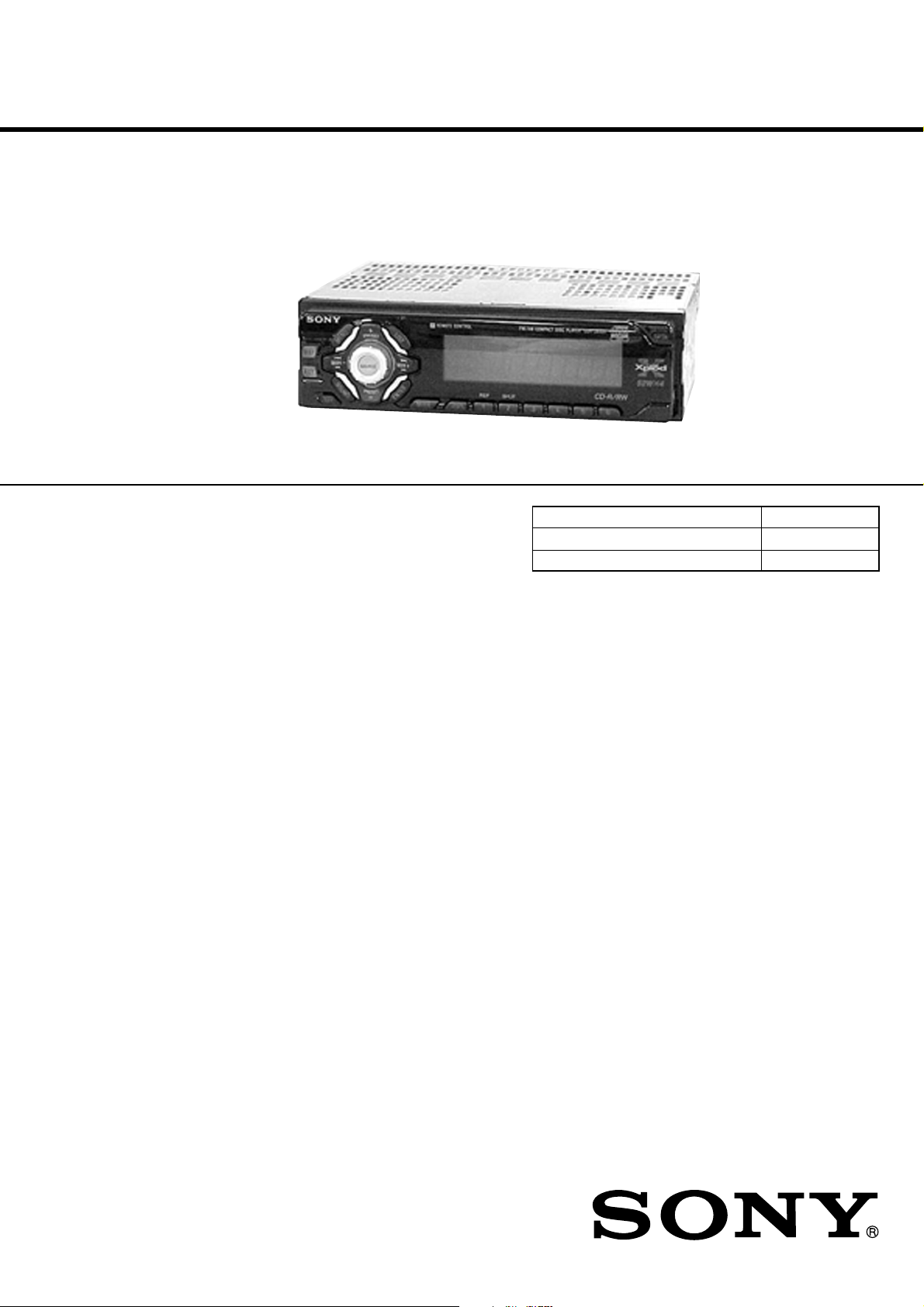
Photo: CDX-L600X
• The tuner and CD sections have no adjustments.
AUDIO POWER SPECIFICATIONS (US Model)
POWER OUTPUT AND TOTAL HARMONIC DISTORTION
23.2 watts per channel minimum continuous average power into
4 ohms, 4 channels driven from 20 Hz to 20 kHz with no more
than 5% total harmonic distortion.
SPECIFICATIONS
CD player section
Signal-to-noise ratio 90 dB
Frequency response 10 – 20,000 Hz
Wow and flutter Below measurable limit
Laser Diode Properties (US, Canadian Model)
Material GaAlAs
Wavelength 780 nm
Emission Duration Continuous
Laser output power Less than 44.6 µW*
* This output is the value measured at a distance
of 200 mm from the objective lens surface on the
Optical Pick-up Block.
Tuner section
FM
Tuning range 87.5 – 107.9 MHz
Antenna terminal External antenna connector
Intermediate frequency 10.7 MHz/450 kHz
Usable sensitivity 8 dBf
Selectivity 75 dB at 400 kHz
Signal-to-noise ratio 66 dB (stereo),
72 dB (mono)
Harmonic distortion at 1 kHz
0.6% (stereo),
0.3% (mono)
Separation 35 dB at 1 kHz
Frequency response 30 – 15,000 Hz
AM
Tuning range 530 – 1,710 kHz
Antenna terminal External antenna connector
Intermediate frequency 10.7 MHz/450 kHz
Sensitivity 30 µV
US Model
Canadian Model
CDX-L600X
E Model
CDX-L630X
Model Name Using Similar Mechanism CDX-L300/L460X
CD Drive Mechanism Type MG-393XA-121//K
Optical Pick-up Name KSS-720A
Power amplifier section
Outputs Speaker outputs
(sure seal connectors)
Speaker impedance 4 – 8 ohms
Maximum power output 52 W × 4 (at 4 ohms)
General
Outputs Audio outputs
Power antenna relay control lead
Power amplifier control lead
Input Telephone ATT control lead
Tone controls Bass ±10 dB at 62 Hz (CDX-L600X)
Bass ±8 dB at 100 Hz (CDX-L630X)
Treble ±10 dB at 16 kHz (CDX-L600X)
Treble ±8 dB at 10 kHz (CDX-L630X)
Loudness +8 dB at 100 Hz
+2 dB at 10 kHz
Power requirements 12 V DC car battery
(negative ground)
Dimensions Approx. 178 × 50 × 176 mm
(7 1/8 × 2 × 7 in.) (w/h/d)
Mounting dimensions Approx. 182 × 53 × 161 mm
(7 1/4 × 2 1/8 × 6 3/8 in.) (w/h/d)
Mass Approx. 1.2 kg
(2 lb. 10 oz.)
Supplied accessories Parts for installation and connections (1 set)
Front panel case (1)
Card remote commander RM-X114
Note
This unit cannot be connected to a digital preamplifier or an equalizer.
Design and specifications are subject to change without
notice.
9-873-403-01
2001K0400-1
© 2001. 11
FM/AM COMPACT DISC PLAYER
Sony Corporation
e Vehicle Company
Published by Sony Engineering Corporation
1
Page 2
CDX-L600X/L630X
k
SERVICE NOTES
NOTES ON HANDLING THE OPTICAL PICK-UP BLOCK
OR BASE UNIT
The laser diode in the optical pick-up block may suffer electrostatic
breakdown because of the potential difference generated by the
charged electrostatic load, etc. on clothing and the human body.
During repair, pay attention to electrostatic breakdown and also use
the procedure in the printed matter which is included in the repair
parts.
The flexible board is easily damaged and should be handled with
care.
NOTES ON LASER DIODE EMISSION CHECK
The laser beam on this model is concentrated so as to be focused on
the disc reflective surface by the objective lens in the optical pickup block. Therefore, when checking the laser diode emission, observe from more than 30 cm away from the objective lens.
Notes on Chip Component Replacement
• Never reuse a disconnected chip component.
• Notice that the minus side of a tantalum capacitor may be dam-
aged by heat.
CAUTION
Use of controls or adjustments or performance of procedures
other than those specified herein may result in hazardous
radiation exposure.
If the optical pick-up block is defective, please replace the whole
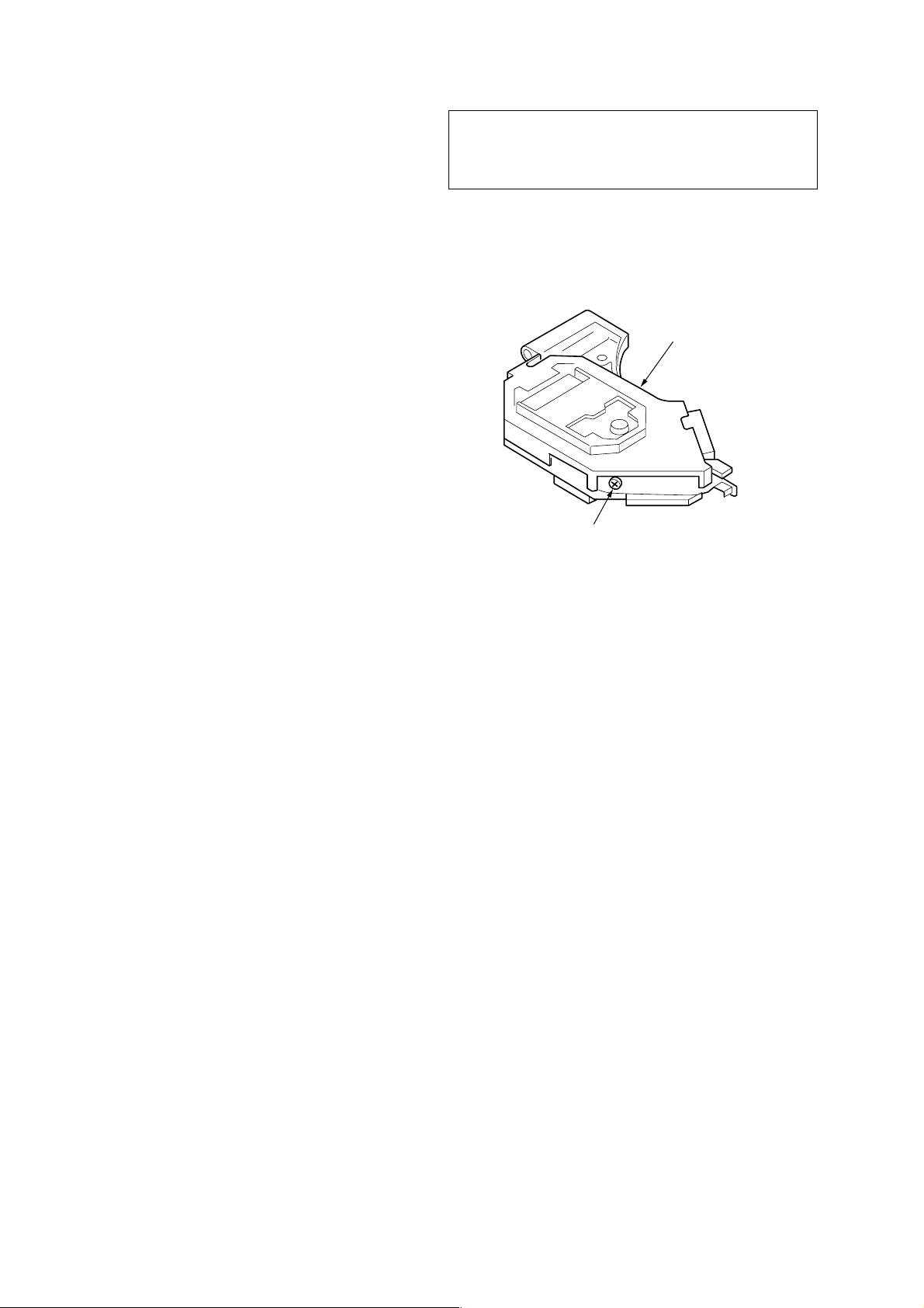
optical pick-up block.
Never turn the semi-fixed resistor located at the side of optical
pick-up block.
optical pick-up bloc
semi-fixed resistor
TEST DISCS
This set can playback CD-R and CD-ROM discs. The following
test discs should be used to check the capability:
CD-R test disc TCD-R082LMT (Part No. J-2501-063-1)
CD-RW test disc TCD-W082L (Part No. J-2501-063-2)
SAFETY-RELATED COMPONENT WARNING!!
COMPONENTS IDENTIFIED BY MARK 0 OR DOTTED LINE
WITH MARK 0 ON THE SCHEMATIC DIAGRAMS AND IN
THE PARTS LIST ARE CRITICAL TO SAFE OPERATION.
REPLACE THESE COMPONENTS WITH SONY P ARTS WHOSE
PART NUMBERS APPEAR AS SHOWN IN THIS MANUAL OR
IN SUPPLEMENTS PUBLISHED BY SONY.
2
ATTENTION AU COMPOSANT AYANT RAPPORT
À LA SÉCURITÉ!!
LES COMPOSANTS IDENTIFIÉS P AR UNE MARQUE 0 SUR LES
DIAGRAMMES SCHÉMATIQUES ET LA LISTE DES PIÈCES
SONT CRITIQUES POUR LA SÉCURITÉ DE FONCTIONNEMENT.
NE REMPLACER CES COMPOSANTS QUE PAR DES PIÈCES
SONY DONT LES NUMÉROS SONT DONNÉS DANS CE MANUEL
OU DANS LES SUPPLÉMENTS PUBLIÉS PAR SONY.
Page 3
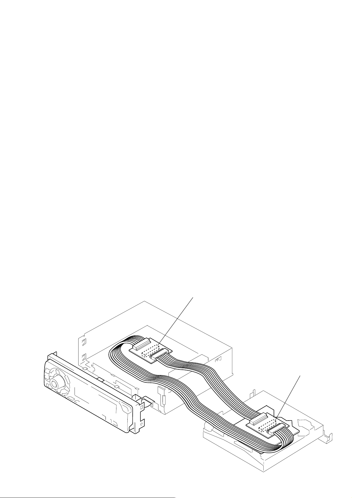
TABLE OF CONTENTS
CDX-L600X/L630X
1. GENERAL
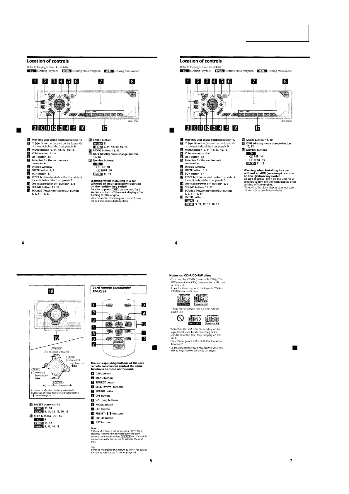
Location of controls (CDX-L600X)........................................4
Location of controls (CDX-L630X)........................................ 4
Connections (CDX-L600X) .................................................... 5
Connections (CDX-L630X) .................................................... 6
2. DISASSEMBLY
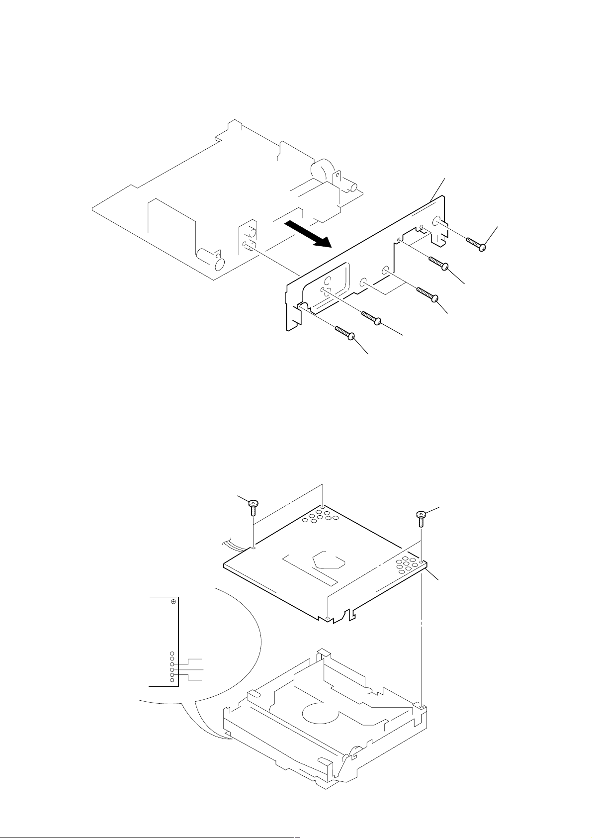
2-1. Sub Panel (CD) Assy........................................................... 7
2-2. CD Mechanism Block ......................................................... 8
2-3. Main Board ......................................................................... 8
2-4. Heat Sink (Main)................................................................. 9
2-5. Chassis (T) Sub Assy .......................................................... 9
2-6. Lever Section .................................................................... 10
2-7. Servo Board....................................................................... 10
2-8. Shaft Roller Assy .............................................................. 11
2-9. Floating Block Assy .......................................................... 11
2-10. Optical Pick-up Block ....................................................... 12
3. DIAGRAMS
3-1. IC Pin Description............................................................. 13
3-2. Block Diagram –CD Section–........................................... 15
3-3. Block Diagram –Tuner Section–.......................................16
3-4. Block Diagram –Display Section–.................................... 17
3-5. Circuit Boards Location .................................................... 17
3-6. Printed Wiring Boards –CD Mechanism Section–............ 18
3-7. Schematic Diagram –CD Mechanism Section– ................ 20
3-8. Printed Wiring Board –Main Section–..............................21
3-9. Schematic Diagram –Main Section (1/2)– ........................ 22
3-10. Schematic Diagram –Main Section (2/2)– ........................ 23
3-11. Printed Wiring Board –Relay Section– ............................. 24
3-12. Schematic Diagram –Relay Section–................................ 25
3-13. Schematic Diagram –Display Section–............................. 26
3-14. Printed Wiring Board –Display Section– .......................... 27
4. EXPLODED VIEWS
4-1. Chassis Section ................................................................. 30
4-2. Front panel Section ........................................................... 31
4-3. CD Mechanism Section (1) ............................................... 32
4-4. CD Mechanism Section (2) ............................................... 33
4-5. CD Mechanism Section (3) ............................................... 34
5. ELECTRICAL PARTS LIST ........................................ 35
EXTENSION CABLE AND SERVICE POSITION
When repairing or servicing this set, connect the jig (extension cable)
as shown below.
• Connect the MAIN board (CNP701) and the SERVO boar d (CN1)
with the extension cable (Part No. J-2502-062-1).
MAIN BOARD CNP701
SERVO BOARD CN1
3
Page 4
CDX-L600X/L630X
SECTION 1
GENERAL
(CDX-L600X) (CDX-L630X)
This section is extracted
from instruction manual.
4
Page 5
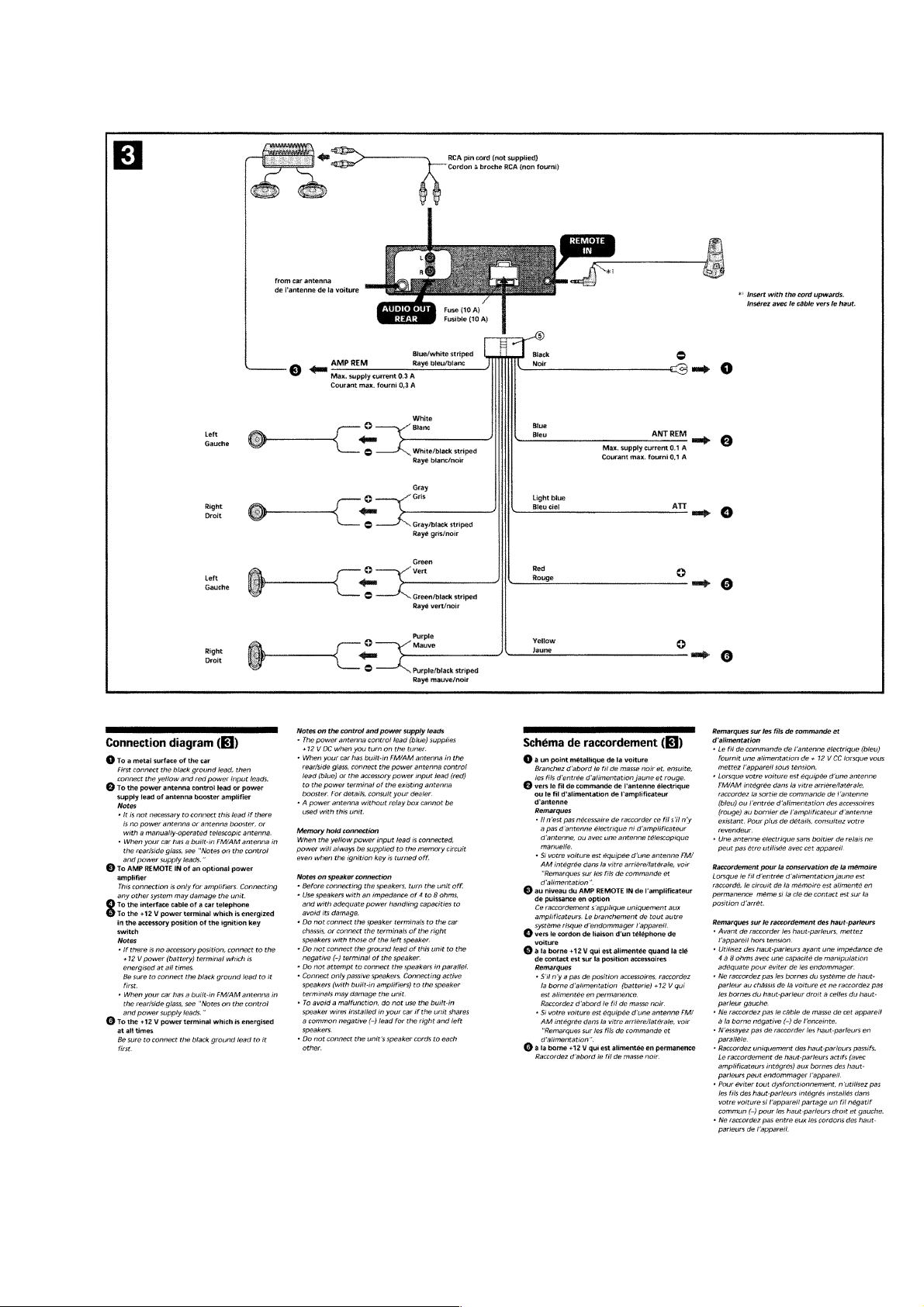
Connections (CDX-L600X)
CDX-L600X/L630X
5
Page 6
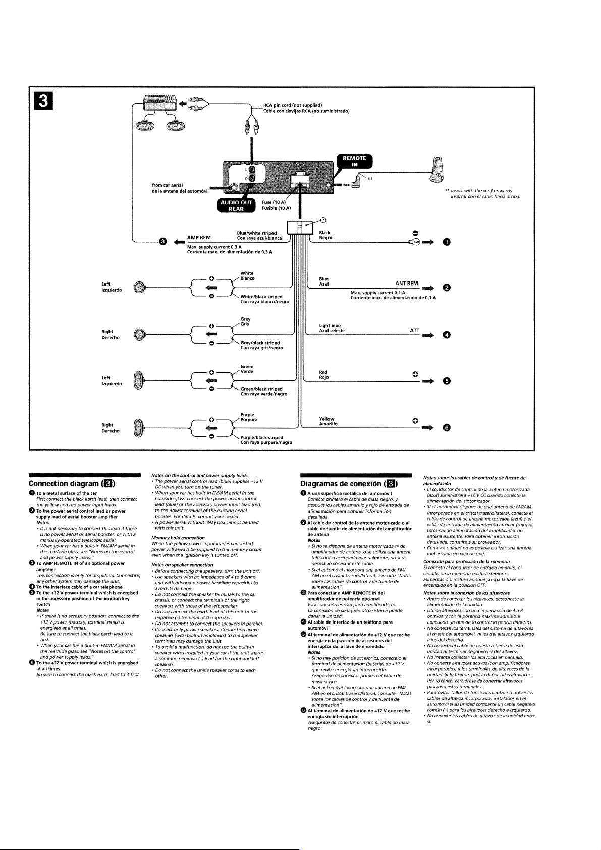
CDX-L600X/L630X
Connections (CDX-L630X)
6
Page 7
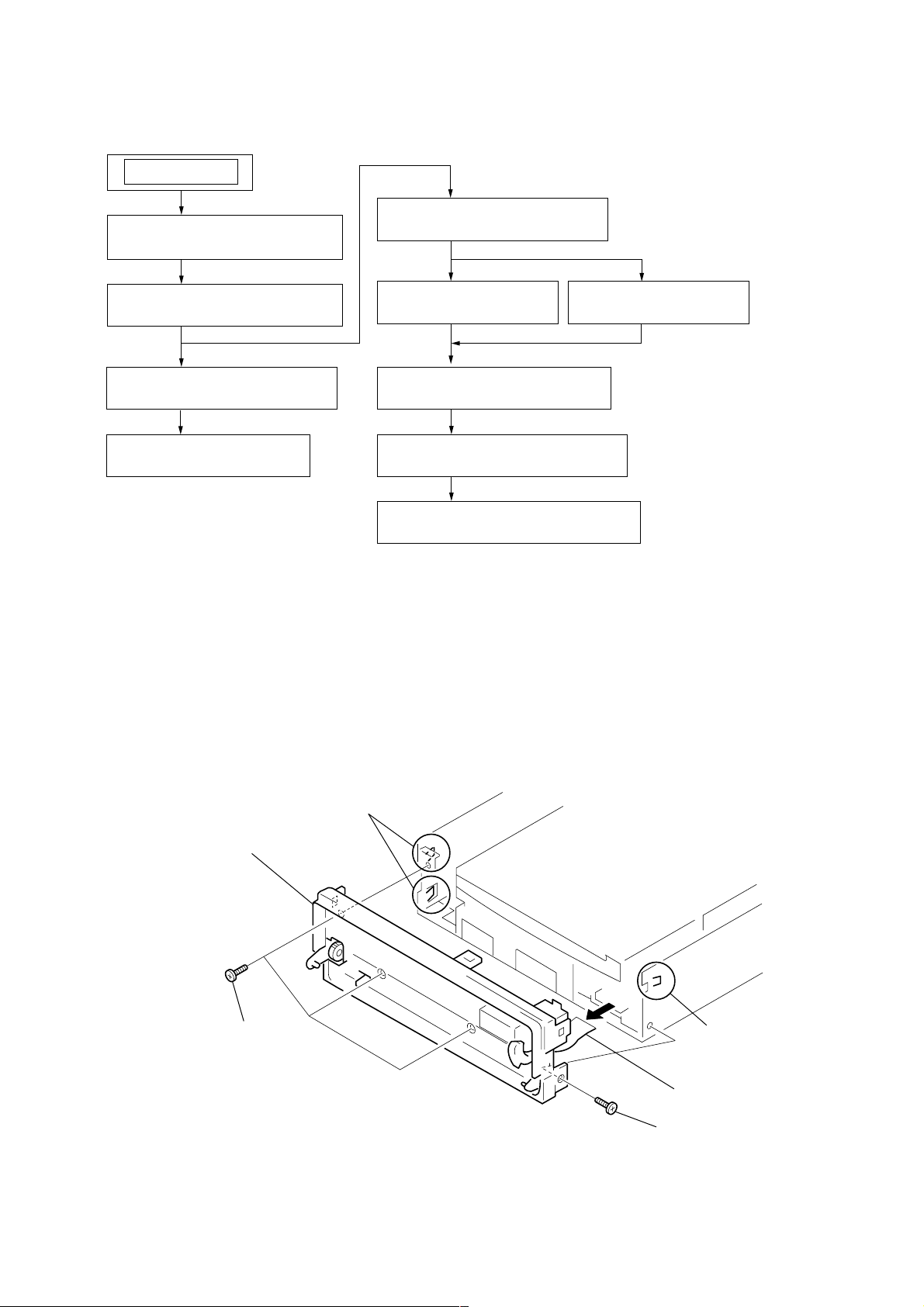
SECTION 2
DISASSEMBLY
Note : This set can be disassemble according to the following sequence.
SET
2-5. CHASSIS (T) SUB ASSY
2-1. SUB PANEL (CD) ASSY
(Page 7)
(Page 9)
CDX-L600X/L630X
2-2. CD MECHANISM BLOCK
(Page 8)
2-3. MAIN BOARD
(Page 8)
2-4. HEAT SINK (MAIN)
(Page 9)
2-6. LEVER SECTION
(Page 10)
2-8. SHAFT ROLLER ASSY
(Page 11)
2-9. FLOATING BLOCK ASSY
(Page 11)
2-10. OPTICAL PICK-UP BLOCK
(Page 12)
Note : Follow the disassembly procedure in the numerical order given.
2-1. SUB PANEL (CD) ASSY
2-7. SERVO BOARD
(Page 10)
6
sub panel (CD) assy
2
PTT 2.6x6
4
two claws
5
CNP802
1
PTT 2.6x6
3
claw
7
Page 8
CDX-L600X/L630X
8
6
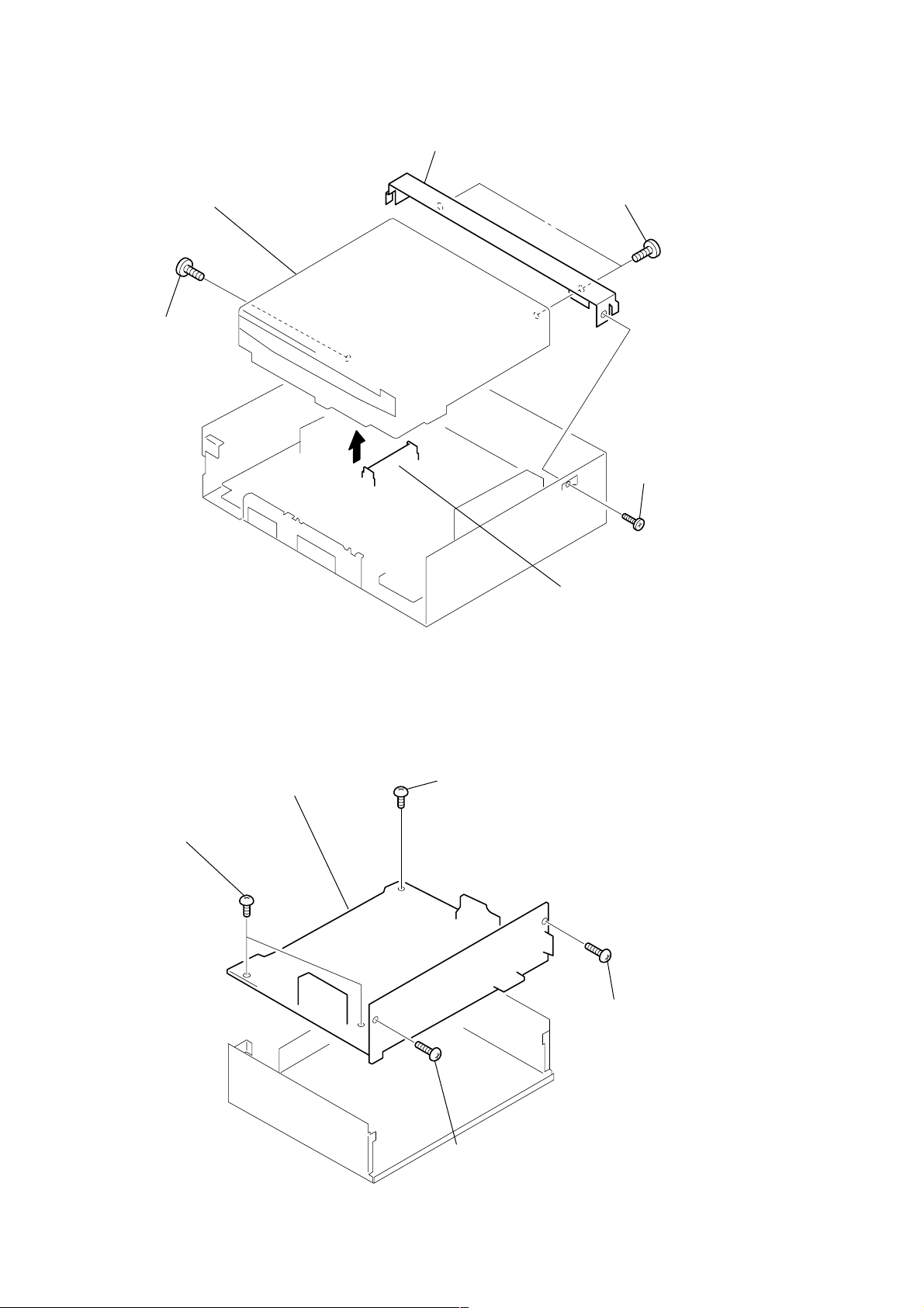
2-2. CD MECHANISM BLOCK
5
CD mechanism block
2
PTT 2.6x6
3
7
bracket (CD)
6
PTT 2.6x6
1
PTT 2.6x
2-3. MAIN BOARD
4
screws (+BTT)
5
MAIN board
3
screw (+BTT)
4
CNP701
2
PTT 2.6x
1
PTT 2.6x8
8
Page 9
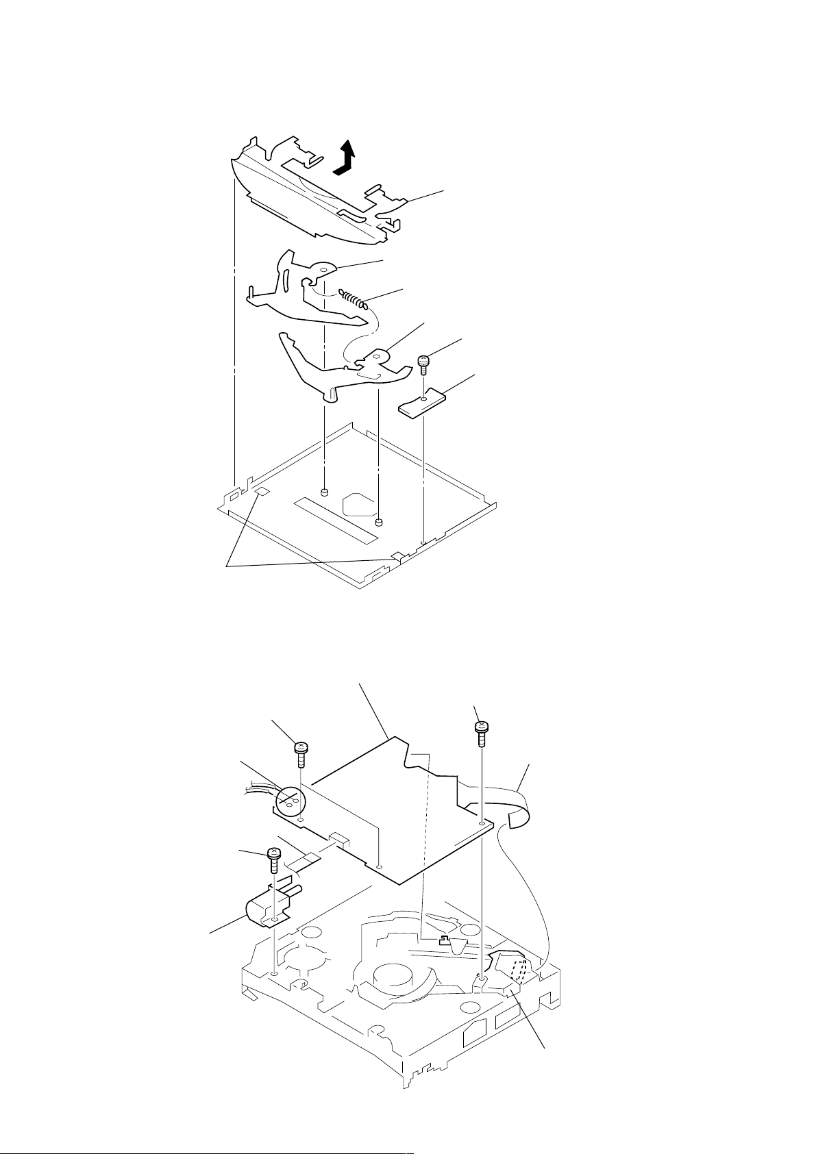
6
heat sink (main)
1
PTT 2.6x8
2
PTT 2.6x8
4
PTT 2.6x8
3
PTT 2.6x12
5
PTT 2.6x8
2-4. HEAT SINK (MAIN)
CDX-L600X/L630X
2-5. CHASSIS (T) SUB ASSY
1
Unsolder the
lead wires.
2
P 2x3
black
red
white
3
P 2x3
4
chassis (T) sub assy
9
Page 10
CDX-L600X/L630X
k
2-6. LEVER SECTION
6
lever (R)
3
tension spring (LR)
7
lever (L)
5
guide (disc)
1
special screw
2
IN SELF SW board
2-7. SERVO BOARD
2
4
loading motor assy
4
claws
5
special screws
Removal the solders.
1
CN3
3
P 2x3
7
SERVO board
6
special screw
8
connector
10
optical pick-up bloc
Page 11
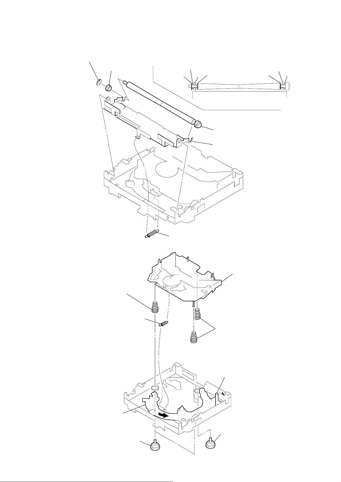
Fig. 1
1
tension spring (RA)
2
arm (roller)
3
retaing ring (RA)
4
shaft retainer
5
shaft roller assy
retaing ring (RA)
arm
arm
washer
washer
shaft retainer
shaft retainer
2-8. SHAFT ROLLER ASSY
• When installing, take note of the positions
arm (roller) and washers. (Fig. 1)
CDX-L600X/L630X
2-9. FLOATING BLOCK ASSY
7
5
direction of the arrow.
compression spring (FL)
1
tension spring (KF1)
Turn loading ring in the
6
floating block assy
8
compression spring (FL)
4
Fit lever (D) in the
direction of the arrow.
3
damper (T)
2
damper (T)
11
Page 12
CDX-L600X/L630X
2-10. OPTICAL PICK-UP BLOCK
1
P 2x3
2
sled motor assy
6
shaft (feed) assy
4
P 2x3
5
spring (feed), plate
3
optical pick-up block
12
Page 13
CDX-L600X/L630X
SECTION 3
DIAGRAMS
3-1. IC PIN DESCRIPTION
• IC801 MN101C49KTG1 (SYSTEM CONTROL)
Pin No. Pin Name I/O Pin Description
1 VREF– — Ground for A/D converter power supply
2 VSM I S-meter voltage detection signal input from tuner unit (TU601)
3 NIL I Connect to ground.
4 KEYIN1 I Key signal input
5 KEYIN0 I Key signal input
6 RC IN0 I Rotary commander key signal input from remote in jack (CNP801)
7, 8 NIL I Not used. (Connect to ground.)
9 DSTSEL I Destination set up detection signal input (“L”: CDX-L600X, “H”: CDX-L630X)
10 VREF+ — A/D converter power supply
11 VDD — Power supply (+5 V) input pin
12 OSCOUT O High speed clock signal output (18.432 MHz)
13 OSCIN I High speed clock signal input (18.432 MHz)
14 VSS — Ground for power supply
15 XIN I Low speed clock signal input (32.768 kHz)
16 XOUT O Low speed clock signal output (32.768 kHz)
17 MMOD I
18 LCDSO O LCD serial data signal output to LCD driver (IC501)
19 LCDCE O LCD chip enable signal output to LCD driver (IC501)
20 LCDCKO O LCD serial clock signal output to LCD driver (IC501)
21 CD SO/TSO O CD servo IC serial data signal output
22 CD SI/TSI I CD servo IC serial data signal input
23 CD CKO/TCKO O CD servo IC serial clock signal output
24 SYSRST O System reset signal output to bus interface (IC803)
25 BUS ON O Bus on signal output to bus interface (IC803)
26 KEYACK I Key acknowledge detection signal input
27 NIL I Not used. (Connect to ground.)
28 BU IN I Back up current detection signal input
29 SIRCS I Remote signal input from remote control receiver (IC502)
30 CD SELFSW I CD mechanism self load position detection switch signal input from self switch (SW2)
31 CD PACK I CD text pack sync signal input from CD servo (IC1)
32 NIH I Connect to power supply.
33 RESET I microcomputer reset signal input from reset IC (IC802) “L”: reset
34 NOSE SW I Front panel attachment detection signal input from nose detect switch (S902) “L”: ON
35 BEEP O Beep signal output to power amp (IC404)
36 NCO O Not used. (Open)
37 TESTIN I Test mode detection signal input
38 ACCIN I Accessory power supply detection signal input
39 NCO O Not used. (Open)
40 TELA TT I Telephone ATT detection signal input
41 NIH I Connect to power supply.
42 BUSSO O Sony-Bus serial data signal output to bus interface (IC803)
43 BUSSI I Sony-Bus serial data signal input from bus interface (IC803)
44 BUSCKO O Sony-Bus serial clock signal output to bus interface (IC803)
45 I2CSIO I/O I2C bus serial data signal input/output
46 NCO O Not used. (Open)
47 I2CCKO O I2C bus serial clock signal output
48 NCO O Not used. (Open)
49 TUNON O Tuner power supply control signal output to power supply (IC901)
50 PW ON O System power supply control signal output to power supply (IC901)
Memory mode select signal input (Input to “Low” (single chip mode).)
(Connect to ground.)
13
Page 14

CDX-L600X/L630X
Pin No. Pin Name I/O Pin Description
51 CD TSTB O CD text parameter strob signal output to servo IC (IC1)
52 CD RFOK I RF OK signal input from servo IC (IC1)
53 CD XRST O Reset signal output to servo IC (IC1)
54 CD A0 O
55 CD STB O Data strob signal output to servo IC (IC1)
56 CD XTALEN O Crystal oscillation control signal output to servo IC (IC1)
57 CD LIMIT I CD Mechanism in-limit switch signal input from limit switch (SW3)
58 CD PH1 I CD Mechanism PH1 detection signal input Not used in this set.
59 CD DSW I CD Mechanism down switch signal input from down switch (SW4)
60 CD INSW/PH2 I CD Mechanism disc-in switch detection signal input from disc-in switch (SW1)
61 CD PH3 I CD Mechanism PH3 detection signal input Not used in this set.
62 CD LM LO O CD Mechanism loading motor control signal output to loading motor drive (IC2)
63 CD LM EJ O CD Mechanism eject motor control signal output to loading motor drive (IC2)
64, 65 NCO O Not used. (Open)
66 AMPATT O Power amp ATT control signal output to power amp (IC404)
67 AMPON O Power amp standby control signal output to power amp (IC404)
68 CDM ON O CD mechanism deck power supply control signal output
69 ATT O System ATT control signal output
70 VOLATT O Electrical volume ATT control signal output to electrical volume (IC401)
71 – 75 NCO O Not used. (Open)
76 4VPRE I Pre-out menu selection set up signal input
77, 78 NCO O Not used. (Open)
79 CD ON O CD on signal output “H”: Play, “L”: Loading or standby
80 – 85 NCO O Not used. (Open)
86 EE SIO I/O EEPROM serial data signal input/output
87 EE CKO O EEPROM serial clock signal output
88 NCO O Not used. (Open)
89 FLASH W I Flash microcomputer write detection signal input “L”: Write mode
90 NCO O Not used. (Open)
91 XKEYON O Key power supply control signal output
92 DOORIND O Sub panel power supply control signal output
93 ILLON O Illumination power supply control signal output
94 DOOR SW I Front panel open/close detection signal input “L”: Close, “H”: Open
95 DAVSS — Ground pin
96 RE IN1 I Rotary encoder signal input from rotary encoder (RE501)
97 RE IN0 I Rotary encoder signal input from rotary encoder (RE501)
98 RC IN1 I
99 NCO O Not used. (Open)
100 DAVDD — Power supply pin (+5 V)
Command/parameter identification signal output to servo IC (IC1)
“L”: Command, “H”: Parameter
Rotary commander shift key signal input from remote in jack (CNP801)
“L”: Shift key on
14
Page 15

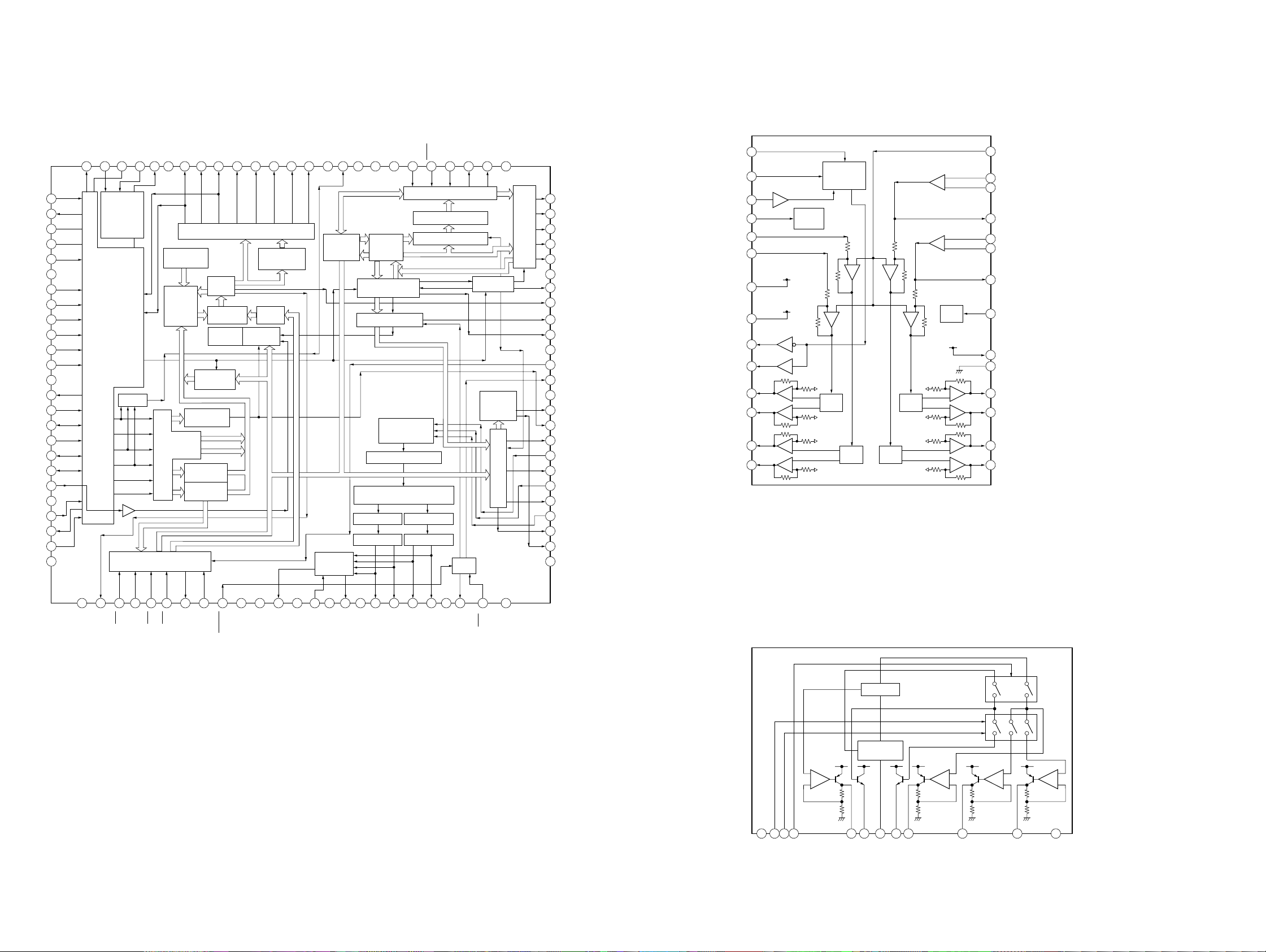
3-2. BLOCK DIAGRAM — CD SECTION —
OPTICAL PICK-UP
KSS-720A
RF AMP,DIGITAL SERVO
DIGITAL SIGNAL PROCESSOR
IC1
CDX-L600X/L630X
PD
LD
A
C
B
D
E
F
FOCUS
COIL
I-V
CONV.
LD
DRIVE
Q1
B
84
D
85
A
82
C
83
E
87
F
86
PD
97
A+5V
LD
98
FOCUS/TRACKING COIL DRIVE,
SLED/SPINDLE/LOADING MOTOR DRIVE
FCS-
15
FCS+
16
APC
IC2
FOCUS
COIL
DRIVE
TRACKING
ERROR
(Page 16)
TUNER
LOUT
RF
EQ
FORCUS
ERROR
FD
26
EFM
DEMOD
SERVO
CTL
FDTDSD
62 63 64 65
MD
D/A
CONV
DSUB CODE
PROCESS
I/F
OSC
23 24
X1
16.9344MHz
ROUT
PACK
TSTB
TSCK
TSI
SCK
STB
RST
RFOK
XTALEN
16
12
R-CH
52
56
55
54
SI
8
SO
7
6
5
AO
4
3
2
9
SW1
(DOWN)
CDL
SECTION
A
SYSTEM CONTROL
31
CD_PACK
51
CD_TSTB
21
CD_SO/TSO
22
CD SI/TSI
23
CD CKO/TCKO
55
CD_STB
54
CD AO
53
CD_XRST
52
CD_RFOK
CD_XTALEN
56
59
CD_DSW
IC801(1/3)
BU_IN
BATT DET
28
Q802,805
OVER VOLTAGE
CHECK
Q803,D803,804
BATT
TRACKING
COIL
M902
(SLED)
M901
(SPINDLE)
M903
(LOADING)
30
CD_SELFSW
CD_INSW/PH2
60
57
CD_LIMIT
CD_LM _LO
62
63
CD_LM_ EJ
68
CDM ON
79
CD_ON
RESET
IC802
33
1
S901
(RESET)
RESET
2
BU+5V
• Signal path
:CD
• R-ch is omitted due to
same as L-ch.
CDM ON
SWITCH
Q908,909
BATT
SW2
(SELF)
SW3
(DISC IN)
SW4
(LIMIT)
CD ON
SWITCH
Q907
TRK+
17
TRK-
18
SL-
M
13
SL+
14
SP+
M
11
SP-
12
LD-
M
9
LD+
10
TRACKING
COIL
DRIVE
SLED
MOTOR
DRIVE
SPINDLE
MOTOR
DRIVE
LOADING
MOTOR
DRIVE
TD
23
SD
5
MD
6
LOAD
1
EJECT
2
A+5V
AU+5V
D+5V
DR+6V
SERVO+5V
REG
Q911,D941
DRIVE+5V
REG
Q910,D931
D932
15 15
Page 16

CDX-L600X/L630X
A
3-3. BLOCK DIAGRAM — TUNER SECTION —
PJ401
L
1
FL+
9
FL-
AUDIO OUT REAR
R
ELECTRONIC VOLUME
IC401
AUX LCH
4
CDRR-CH
42
MD RCH
OUT FL
28
POWER AMP
12
IC404
R-CH
CNP902
5
3
PJ601
(ANTENNA)
TUNER UNIT
TU601
ANTFM MPX
2 10
AM DET
ANTAM
1
S-METER
I2C SDA
I2C SCL
E2PROM SDA
E2PROM SCL
CD
(Page 15)
8
SECTION
CDL
14
12
13
17
18
MD LCH
43
MPX1
12
AM/MPX2
9
LEVEL(VSM)
13
MPIN
14
SDA
19
SCL
20
EXA ATT
17
SYSTEM CONTROL
IC801 (2/3)
VOL ATT
70
VSM
2
I2C SIO
45
I2C CKO
47
DSTSEL
9
EE SIO
86
EE CKO
87
OUT RL
OUT FR
OUT RR
ATT
BEEP
AMP ON
AMP ATT
TEL ATT
ACC IN
TEST IN
TUN ON
PW ON
27
Q102
MUTE
26
25
69
35
67
66
40
38
37
49
50
R-CH
Q912,913
MUTE
CONT
Q101
MUTE
R-CH
D908
DELAY BATT
ACC
CHECK
Q902, D934, 935
POWER SUPPLY
IC901
2
8.7V ON
3
5.6V ON
4
STB
11
AUX
16
STBY
4
MUTE
22
TEL
ATT
Q901
6
AMP +B
8
ANT +B
7
VCC
5
BU+B BU 5V
9
COM 8V
10
TU 5.6V
11
TU 8.7V
D919
D907
BATT
COM 8V
TU 5.6V
TU 8.7V
9
7
R-CH
F901
10A
2
RL+
10
RL-
4
FR+
12
FR-
3
RR+
11
RR-
13
ATT
7
ACC
15
TEST
5
AMP R
6
ANT R
8
GND
19
17
18
+B (BATT)
16
• Signal path
:FM
:AM
:CD
• R-ch is omitted due to same as L-ch.
1616
Page 17

CDX-L600X/L630X
3-4. BLOCK DIAGRAM — DISPLAY SECTION —
SYSTEM CONTROL
IC801 (3/3)
KEY IN0
KEY MATRIX
LSW501-510,
LSW513-522
LSW916(1/2)
CNP801
(REMOTE IN)
D801
D802
S902
(NOSE DET)
KEY
ACTIVE
Q801
IC502
IR
RECEIVE
ROTARY
ENCODER
RE501
X802
32.768kHz
5
26
91
98
6
29
97
96
34
15
16
KEY IN1
KEY ACK
XKEYON
RC IN1
RC IN0
SIRCS
RE IN0
RE IN1
NOSE SW
XIN
XOUT
LCD SO
LCD CKO
LCD CE
DOOR IND
ILL ON
OSC OUT
OSC IN
3-5. CIRCUIT BOARDS LOCATION
LCD DRIVE
IC501
80
SEG2
SEG66
COM1
COM4
SWITCH
Q905
•
|
1
|
64
65
|
|
68
LCD
LCD500
LSW501-510
LSW513-522
LED510-513
KEY
()
ILLUMINATION
LCD BACK
()
LIGHT
RELAY board
DATA
18
20
194
92
93
12
13
LCD DATA
78
CLK
LCD CLK
77
CE
LCD CE
76
DOOR IND
DRIVE
Q914, 915
LED905,LSW916(2/2)
POWER
CONT
Q906
BATT
X801
18.43MHz
IN SELF SW board
DISPLAY board
SL SW board
tuner unit
(TU601)
MAIN board
SERVO board
• Waveforms
— Servo Board —
(MODE: CD PLAY)
— Main Board —
1
2
3
4
5
16.9344MHz
IC1
IC1
IC1
IC1
(XTAL)
wd
34msec
(PACK)
ts
(RFO)
uj
Approx. 100mVp-p
(FEO)
oa
2Vp-p
5Vp-p
1.2Vp-p
0V
1
2
IC801
IC801
18.43MHz
(OSCOUT)
qs
32.768kHz
(XOUT)
qh
1.6Vp-p
5Vp-p
17 17
Approx. 100mVp-p
od
(TEO)
IC1
0V
Page 18

CDX-L600X/L630X
3-6. PRINTED WIRING BOARDS — CD MECHANISM SECTION — • Refer to page 17 for Circuit Boards Location.
THIS NOTE IS COMMON FOR PRINTED WIRING
BOARDS AND SCHEMATIC DIAGRAMS.
(In addition to this, the necessary note is
printed in each block.)
for schematic diagram:
• All capacitors are in µF unless otherwise noted. pF: µµF
50 WV or less are not indicated except for electrolytics
and tantalums.
• All resistors are in Ω and 1/
specified.
• % : indicates tolerance.
f
•
• C : panel designation.
• A : B+ Line.
• Power voltage is dc 14.4V and fed with regulated dc power
• Voltages are taken with a VOM (Input impedance 10 MΩ).
• Waveforms are taken with a oscilloscope.
• Circled numbers refer to waveforms.
• Signal path.
: internal component.
Note:
The components identified by mark 0 or dotted
line with mark 0 are critical for safety.
Replace only with part
number specified.
supply from ACC and BATT cords.
Voltage variations may be noted due to normal produc-
tion tolerances.
Voltage variations may be noted due to normal production tolerances.
F : FM
f : AM
J : CD
4
W or less unless otherwise
Note:
Les composants identifiés par
une marque 0 sont critiques
pour la sécurité.
Ne les remplacer que par une
piéce portant le numéro
spécifié.
CN2
23456789101112
1
A
B
C
D
E
for printed wiring boards:
• X : parts extracted from the component side.
• Y : parts extracted from the conductor side.
• x : parts mounted on the conductor side.
a
•
• : Pattern from the side which enables seeing.
Caution:
Pattern face side: Parts on the pattern face side seen from the
(Side B) pattern face are indicated.
Parts face side: Parts on the parts face side seen from the
(Side A) parts face are indicated.
: Through hole.
(The other layer’s patterns are not indicated.)
F
G
H
SW1
I
J
1818
Page 19

CDX-L600X/L630X
A
B
C
D
E
F
G
H
1
I
234567891011121314
• Semiconductor
Location
Ref. No. Location
IC1 E-7
IC2 H-7
Q1 C-6
SW4
TP66
TP73
TP53
TP64
TP86
TP87
TP75
TP47
TP69
TP57
R20
R22
FB6
R21
TP68
TP54
TP76
FB7
FB3
TP48
TP85
TP50
TP51
TP52
TP56
TP58
TP61
TP74
TP62
CN1
TP49
TP7
C44
TP91
TP90
TP19
CN3
TP63
TP60
TP59
TP71
R17
TP72
TP80
TP8
R19
C26
TP77
R26
C4
TP9
TP70
C40
TP55
C27
FB1
C37
TP20
TP78
R30
Q1
R3
C6
C25
C34
C1
R29
C3
R18
C41
C45
X1
TP92
TP17
C29
R7
R6
TP16
TP79
C17
C22
C21
C5
C43
C9
C16
C36
TP34
TP11
TP36
C10
C8
R24
R25
TP12
TP35
FB4
FB2
C15
IC1
TP46
C38
TP39
IC2
TP82
TP81
C11
C14
TP45
TP37
TP38
TP40
TP30
TP83
TP43
TP42
TP32
R15
R12
R10
TP26
C30
TP28
TP27
TP84
C13
C18
TP23
C35
TP41
TP29
R5
R9
TP44
TP21
TP10
TP89
TP88
TP18
TP3
TP2
TP1
C20
C19
R8
R14
C23
C24
TP22
TP24
TP25
TP6
SW3
(Page 21)
SW2
TP5
TP4
J
19 19
Page 20

CDX-L600X/L630X
• Refer to page 17 for Waveforms.
3-7. SCHEMATIC DIAGRAM — CD MECHANISM SECTION — • Refer to page 28 for IC Block Diagrams.
CN2
Q1
TP9 TP8
R3 R26
C3 C6
C4
TP7
TP92
C14
TP10
C13
C11
R5
C15
C10
TP12 C9
TP11
C8
C16
R7
TP21
TP18
R6
TP17
TP20
TP16
TP19
M902
M901
SW4
SW3
SW2
CN13
M903
TP87
TP86
CN3
SW1
TP4
TP2
TP3
TP77
TP78
C1 C5
TP81
TP82
TP83
TP84
TP85
TP1
TP5
R29
R30
TP79
TP80
C43
IC B/D
C40
TP6
R24
R25
C22
C21
TP89
C17
C18
C19
C20 C23
R9
IC2
FB4
C35
FB2
C36
TP45
TP44
TP43
TP42
TP41
TP40
TP39
TP38
TP37
TP46
TP36
TP35
TP34
C38
C44
FB3
R22
R21
FB7
FB6
R18
R19
R20
R17
TP66
TP61
TP76
TP60
TP75
TP59
TP74
TP58
TP73
TP57
TP72
TP56
TP71
TP55
TP70
TP54
TP69
TP53
TP68
TP52
TP51
TP50
TP64
TP49
TP48
TP63
TP47
TP62
CN1
(Page 22)
C24
R12
R10
C26
C30
C27
TP30
R15
TP27
TP29
TP26
TP28
TP88
R14
C45
TP91
C29
C34
TP32
TP90
C25
X1
C37
TP24
TP25
TP22
TP23
R8
IC1
FB1
C41
IC B/D
Note:
• Voltage is dc with respect to
ground under no-signal conditions.
no mark : CD PLAY
2020
Page 21

3-8. PRINTED WIRING BOARD — MAIN SECTION — • Refer to page 17 for Circuit Boards Location.
CDX-L600X/L630X
A
B
C
D
E
F
G
H
1
C603
R601
C604
C605
JW14
JR602
D601
I
JW1
JW2
2 3 4 5 6 7 8 9 10 11 12 13 14 15
PJ401
CNP902
D918
R923
X802
D917
C405
C907
D935
C865
JW107
JW62
F901
D913
JW79
JW80
R927
R913
JW106
JW113
JW115
JW117
JW119
JW120
JW121
C805
D914
JW72
Q901
JW89
JW95
JW100
JW101
R808
JW123
JW124
JW125
C914
C908
C928
R917
JW103
JW104
JW105
JW111
JW118
R868
R867
JW75
Q902
D907
D919
JW98
JW81
JW82
JW83
JW84
R866
JW116
C810
R901
R821
R858
Q802
Q805
R837
Q801
C932
JW77
D906
C814
R924
D920
JW96
JW97
JW112
JW76
JW85
JW90
JW102
IC802
R852
S902
JW63
JW64
JW65
JW73
JW74
JW93
JW94
R865
R833
Q803
R862
JW66
JW67
JW68
JW78
D932
D901
R836
C809
D804
JW126
D803
JW127
Q907
JW128
S901
Q908
JW91
Q914
Q915
R827
Q905
JW129
JW69
Q909
R828
R835
R834
R921
R919
JW132
Q906
C933
R920
JW92
R925
R926
C816
R928
JW70
L900
IC901
JW122
R937
R936
R935
R934
JW130
C815
Q910
D931
C919
JW71
JW131
• Semiconductor Location
Ref. No. Location
D601 H-1
D801 I-5
D802 I-6
D803 H-10
D804 H-10
D814 J-3
D815 I-2
D816 J-3
D901 G-10
D906 D-9
D907 E-9
D908 D-7
D911 B-7
D912 B-7
D913 C-8
D914 C-8
D915 B-8
D916 B-8
D917 C-8
D918 B-8
D919 F-9
D920 C-9
D931 C-11
D932 E-10
D934 D-8
D935 D-8
D941 F-8
Ref. No. Location
IC401 G-3
IC404 B-6
IC801 H-7
IC802 H-9
IC901 G-11
Q101 C-4
Q102 C-3
Q201 C-4
Q202 C-3
Q801 I-9
Q802 H-9
Q803 H-9
Q805 H-9
Q901 E-8
Q902 D-8
Q905 I-10
Q906 I-10
Q907 G-10
Q908 E-10
Q909 E-10
Q910 C-11
Q911 F-8
Q912 D-6
Q913 D-7
Q914 G-10
Q915 G-10
C607
R604
C611
JW6
JW5
R610
TU601
C606
R608
C612
JR704
JW3
C601
C608
R602
R701
JW4
D815
R609
C703
C610
R861
R856
JR803
R611
C701
C702
JW7
JW45
C112
R124
C122
JW41
JR701
D816
JW46
R114
C212
IC401
C705
CNP802
D814
R125
Q102
JR804
R224
C222
JW28
JW47
R214
JW29
C101
C201
JW40
JW31
JR702
R225
JW49
JW43
R111
R211
JW42
JR411
JR105
R816
C455
Q202
C706
R115
Q101
JW48
JR203
JR103
JR202
JR107
R121
R221
C465
JR412
JW11
R803
R805
JR806
JW38
JW15
JR102
JW17
JW8
R825
R822
R804
R215
Q201
JW50
JR101
JW9
R128
JR901
R228
JR104
JW10
R820
R817
C812
R118
JR201
JW133
R826
R818
R823
JR204
R819
C403
JW16
JW12
R801
R864
JR801
R218
C223
D801
JR106
JW13
R863
C113
C213
C123
JW52
JW18
JW53
C404
C471
R404
JR301
JR108
C868
JW51
C866
R842
R857
JW19
JW59
IC404
JW54
JW37
JW36
JW35
R814
JW34
JW33
JW32
C867
R402
JR802
R843
R845
JW20
JR703
R854
R844
R403
JW21
JW60
C402
JW22
R908
JW23
D802
CNP905
C934
R815
R813
JW24
JW58
R812
C476
CNP701
R811
JW25
JW55
C930
R930
JW26
Q912
JW61
Q913
JW136
R810
JW27
C915
JW57
R839
C709
IC801
C710
C708
C801
C916
D909
R840
R855
D912
R907
R909
R910
R841
R807
R911
JW88
R702
D911
R401
D908
JW99
R802
D916
CNP906
R906
C905
R915
R912
JW86
JW87
R703
R806
JW110
JW114
C806
C929
X801
JR805
D915
C906
R916
Q911
R922
JW109
D934
R914
C921
D941
JW108
C804
J
(Page 24)
(Page 19)
21 21
Page 22

CDX-L600X/L630X
• Refer to page 17 for Waveforms.
3-9. SCHEMATIC DIAGRAM — MAIN SECTION (1/2) — • Refer to page 29 for IC Block Diagrams.
C201
JR703
JR803
C101
C706
C701
R701
PJ601
R610
C601
C603
R601
TU601
JR704
R602
C611
C608
R608
C612
C607
R609
R604
R611
C604
JR602
C605
C610
D601
C606
C702
C703
IC401
JR701
C705
JR702
IC B/D
R111
R121
R211
R221
Note:
• Voltage is dc with respect to ground under
no-signal (detuned) condition.
no mark : FM
( ) : AM
< > : CD PLAY
JR105
JR106
JR107
JR108
JR301
JR411
JR101
JR102
JR201
JR202
(Page 20)
CNP701
R922
R923
C710
D941
C708
C709
Q911
R703
JW
C921
88
R919
R920
R921
R928
R702
C919
Q910
D931
D932
C865
Q907
C867
R841
R840
R908
R854
Q909
R839
R810
R811
R812
R815
R813
JR802
Q908
R857
R842
R843
R855
R844
R845
C866
R821
IC801
R861
C868
R863
R864
C806
R820
C929
R819
R808
JR805
R802
X802
C801
R867
R868
R807
R806
R805
R804
R803
C805
C804
R817
R818
R801
X801
R814
R822
R823
Q801
S901
R862
(Page 23)
R852
R924
S902
2222
Page 23

3-10. SCHEMATIC DIAGRAM — MAIN SECTION (2/2) — • Refer to page 28 for IC Block Diagrams.
CDX-L600X/L630X
C112
C122
C212
C222
R114
R124
R214
R224
R115
R125
R215
R225
Q101
Q102
Q201
Q202
JR901
JR412
JR103
JR104
JR204
JR203
R402
R403
R401
R404
R118
R128
R228
R218
C405
C471
C113
C123
C223
C213
C402
C404
IC404
C403
C476
D915
D916
D917
D918
D913
D914
D911
D912
C914
D906
D920
JR804
R836
D802
R901
L900
C908
C907
R834
R835
C455
C465
C906
C816
PJ401
CNP902
CNP801
C815
(Page
22)
C934
Q912
R930
Q913
C915
C930
D908
D909
C916
C932
R906
R907
IC802
C928
R917
C809
Q902
R916
C810
R915
C814
C905
JR801
R914
D901
D935
R934
D934
R935
IC901
R936
R927
R913
Q906
R937
Q905
R926
R912
C933
Q901
R925
R911
Q914
R910
IC B/D
D907
D919
R909
Q915
R837
Q805
Q802
R825
R826
D801
R833
D803
D804
D814
Q803
R827
R828
D815
D816
R816
JR806
R856
R866
C812
R865
R858
CNP802
(Page 25)
23 23
Note:
• Voltage is dc with respect to
ground under no-signal
(detuned) condition.
no mark : FM
Page 24

CDX-L600X/L630X
3-11. PRINTED WIRING BOARD — RELAY SECTION — • Refer to page 17 for Circuit Boards Location.
A
B
C
D
1
LSW916
2 3 4 5 6 7 8 9 10 11 12 13 14 15
LED905
R932
R930
R931
E
F
G
H
(Page 21)
CNP902
I
(Page 27)
J
2424
Page 25

3-12. SCHEMATIC DIAGRAM — RELAY SECTION —
CNP902
CDX-L600X/L630X
CNP903
(Page 26)
LSW
916(1/2)
LSW
916(2/2)
LED905
(Page 23)
R931
R930
R932
25 25
Page 26

CDX-L600X/L630X
3-13. SCHEMATIC DIAGRAM — DISPLAY SECTION —
RE501
(Page 25)
CN501
D503
R514
LSW
501
D501
R515
LSW
D502
513
LED510
LED511
R552
R544
R516
LSW
515
R542
R545
LED512
LED513
R543
R517
LSW
516
R553
LSW
LSW
LSW
R546
R518
501
507
R547
517
R548
LSW
LSW
R519
LSW
R549
516
515
518
R550
R551
LSW
R520
519
LSW
LSW
LSW
LSW
R554
505
513
504
508
R521
LSW
R525
520
LSW510
503
LSW
502
LSW
506
LSW
R555
R522
LSW
521
R526
LSW
LSW
LSW
LSW
R556
LSW
R523
521
522
509
514
522
R527
LSW517
518
LSW
519
LSW
520
LSW
R557
R528
R534
C532
IC502
D504
R524
R539
R540
R541
C534
R538
C533
R532
R533
R535
C535
C536
R536
R537
IC501
LSW
514
R501
LSW
502
R502
LSW
503
R503
LSW
504
R504
LSW
505
LSW
R505
506
R506
LSW
507
R507
LSW
508
R508
LSW
R509
509
R510
LSW
LCD500
510
Note:
• Voltage is dc with respect to ground under no-signal
(detuned) condition.
no mark : FM
2626
Page 27

3-14. PRINTED WIRING BOARD — DISPLAY SECTION — • Refer to page 17 for Circuit Boards Location.
CDX-L600X/L630X
A
B
C
D
1
LSW516
LSW515
2 3 4 5 6 7 8 9 10 11 12 13 14 15
LSW502
LSW506
LSW507
LSW513
LSW501
LSW510
LSW503
LSW508
LSW504
IC502
LSW505
LED512
LED513
LSW514
LSW509
LSW522
LCD500
LSW521
LSW520
LSW519
LSW518
LED511
LED510
LSW517
E
F
G
H
I
R517
R507
R506
R526
R555
R501
R502
R503
R516
R546
R550
R549
R504
R547
R505
R548
R551
R525
R515
R554
R514
R508
R509
R524
R527
R510
R556
R553
R544
R543
R545
R552
R542
C533
R537
D504
C532
C535
R533
R534
C534
R538
R535
C536
R536
R523
R522
R521
IC501
R539
R541
R540
D502
R520
D503
R532
D501
R519
CN501
R528
R518
R557
• Semiconductor Location
Ref. No. Location
D501 I-13
D502 H-12
J
D503 G-12
D504 H-7
IC501 H-10
Ref. No. Location
IC502 B-6
LED510 C-14
LED511 B-14
LED512 B-6
LED513 C-6
(Page 24)
27 27
Page 28
CDX-L600X/L630X
+
–
+
–
+
–
+
–
OVER VOLTAGE
PROTECT
REGULATOR
1
2 3
4
5 6 7 8 9 10 1211
NC
MODE2
MODE1
STB
VDD
AMP
VCC
ANT
COM
AM
FM
GND
• IC BLOCK DIAGRAMS
IC1 µPD63711GC-8EU
AGCO74RFI73C3T72ASY71EFM70AVDD697E DAC3687D DAC2677C DAC1667F DAC065MD64SD63TD62FD
75
AGCI
76
RFO
77
EQ2
78
EQ1
79
RF-
80
AGND
81
A
82
C
83
B
84
D
AVDD
REFOUT
FEO
TE-
TEO
TE2
TEC
AGND
AVDD
85
F
86
E
87
88
89
FE-
90
91
92
93
94
95
96
PD
97
LD
98
99
PN
100
AMP BLOCK
DEFECT
MIRR
EFM
COMPARATOR
EFM
FEOFS
TEOFS
RF
EFM
SWITCH
FOK
A3T
FEO
TEO
COMPARATOR
MICROCOMPUTER INTERFACE
AUTO GAIN
CONTROLLER
SVDRAM
PROCESSOR
DEFECT
COMPARATOR
RFENV
MIRENV
TRACKING
A/D CONVERTER
REGISTER
FOCUS
REGISTER
ADDER
MULTIPLIER
SVROM
CLV
D/A
FD/TD/SD/MD
CONTROLLER
SVCRAM
ROM
DECODER
ATEST59TEST158TEST057DGND56TSTB55TSCK54TSI53TSO52PACK51DVDD
AGND
60
61
MICROCOMPUTER INTERFACE
CD-TEXT DECODER
MEMORY
PROCESSOR
16K
SRAM
SUB-CODE PROCESSOR
EFM DEMODULATOR
TIMING GENERATOR
D/A
INTERFACE
CIRCUIT
DE-EMPHASIS CIRCUIT
OCTUPLED
OVERSAMPLING DIGITAL FILTER
NOISE SHAVER
OUTPUT BUFFER
SCF
NOISE SHAVER
OUTPUT BUFFER
OSC
DIGITAL PLL
DIGITAL
AUDIO
INTERFACE
OUTPUT PROCESSOR
ERROR
PROCESSOR
CORRECTION
C2D3
50
C2D2
49
C2D1
48
C1D2
47
C1D1
46
DGND
45
PLCK
44
MIRR/WFCK
43
RFCK
42
LOCK
41
DVDD
40
TSOI
39
C16M
38
DGND
37
TX
36
HOLD/WDCK
35
LRCK
34
LRCKIN
33
SCKO
32
SCKIN
31
DOUT
30
DIN
29
FLAG
28
EMPH
27
DVDD
26
FWD
REV
LDCONT
IN1
IN2
PREVCC
POWVCC
VOL–
VOL+
VO2–
VO2+
VO1–
VO1+
IC2 BA5810FP-E2
1
2
X3
3
PS
4
5
6
7
8
9
10
10k
11
12
10k
10k
13
14
10k
POWER
PREVCC
(PRE.LOADING)
POWVCC12
(CH1.CH2)
–
+
+
–
–
+
+
–
SAVE
10k
10k
10k
10k
LOADING PRE
7.5k
–
16k
LEVEL
SHIFT
FWD REV
7.5k
16k
+
LEVEL
SHIFT
BIAS
28
+
–
+
7.5k
–
+
–
+
–
16k
27
26
25
24
23
22
OPIN4+
OPIN4–
OPOUT4
OPIN3+
OPIN3–
OPOUT3
7.5k
LEVEL
SHIFT
+
LEVEL
SHIFT
–
CH1-4
MUTE
16k
POWVCC34
(CH3,CH4)
10k
10k
10k
10k
–
+
+
–
–
+
+
–
10k
10k
10k
10k
21
20
19
18
17
16
15
MUTE
POWVCC
GND
VO3–
VO3+
VO4–
VO4+
1
2
3
4A05
6
DGND
RFOK
RST
STB
7SO8SI9
SCK
10
XTALEN
DVDD
11
DAVDD
12
ROUT
13
DAGND
REGC
1514
16
DAGND
17
18R+19R–20L+21L–22
LOUT
DAVDD
23
XTAL24XTAL
XVDD
25
XGND
IC901 BA4908-V3
2828
Page 29

IC401 TDA7406T
CDX-L600X/L630X
SWIN
ACINR
ACOUTR
SWACOUT
AC OUTL
CREF
MIXINFL
MIXINRL
MIXINFR
MIXINRR
OUTFL
OUTRL
28 2730 2932 31
MIXER
SOFT STEP
FADER
OUTPUT SELECTOR
HIGH PASS
7BAND
EQUALIZER
SOFT STEP
VOLUME
SOFT MUTE
LOUDNESS
IN GAIN
+ AUTO
ZERO
OUTFR
OUTRR
26 25 24 23
SOFT STEP
FADER
SPECTRUM
ANALIZER
OUTSW
SOFT STEP
FADER
SUB
WOOFER
FILTER
MONO
FADER
BEEP
PAUSE
II
C-BUS
DIGITAL
CONTROL
HIGH OUT
S & H
25kHz
LP
DEMODULATOR
+STEREO ADJUST
+STEREO BLEND
PILOT
CANCELLATION
SAOUT
QUAL.
PIL, DET
PLL
CREF
MULTI
PATH
DETECTOR
SUPPLY
PULSE
FORMER
AM/FM
NOISE
BLANKER
A/D
22
21
20
19
18
17
16
15
14
13
VDD
SACLK
SCL
SDA
GND
ATT
QUAL
MP OUT
MP IN
LEVEL
ACINL
33
34
35
36
37
38
39
CDR
CDL
MDR
MDL
TAPEL
MAIN SOURCE
40
41
42
43
44
SELECTOR
INPUT MULTIPLEXER
1 2 3 4 5 6 7 8 9 10 11
FDL–
FDR+
TAPE R
FDL+
PAUSE
MIXING
SELECTOR
TIM
PHONE
NAVI
86kHz
LP
STD
IN GAIN
AM/MPX2
AMIF
CMPX
12
AUX1
29
Page 30

CDX-L600X/L630X
SECTION 4
EXPLODED VIEWS
NOTE:
• The mechanical parts with no reference
number in the exploded views are not supplied.
• Items marked “*” are not stocked since
they are seldom required for routine service.
Some delay should be anticipated
when ordering these items.
• -XX and -X mean standardized parts, so
they may have some difference from the
original one.
4-1. CHASSIS SECTION
9
8
• Color Indication of Appearance Parts
Example :
KNOB, BALANCE (WHITE) ... (RED)
RR
Parts Color Cabinet’s Color
• Accessories are given in the last of this
parts list.
11
MG-393XA-121//K
10
12
17
13
14
16
15
The components identified by
mark 0 or dotted line with mark
0 are critical for safety.
Replace only with part number
specified.
Les composants identifiés par une
marque 0 sont critiques pour
la sécurité.
Ne les remplacer que par une piéce
portant le numéro spécifié.
#2
#1
#1
#1
#3
#1
#1
#1
4
3
1
2
20
7
5
6
#2
#5
#2
#5
#5
19
Ref. No. Part No. Description Remark
1 X-3380-007-1 PANEL ASSY (CD), SUB
2 3-041-039-02 BUTTON (EJECT)
* 3 1-679-988-11 RELAY BOARD
4 X-3376-686-4 GEAR ASSY
5 3-030-909-03 DAMPER, OIL
21
#2
TU601
#6
12
#2
#2
F901
18
Ref. No. Part No. Description Remark
* 15 3-019-565-01 BRACKET (IC)
16 3-041-261-11 BRACKET (TR)
* 17 3-224-313-01 HEAT SINK (REG)
* 18 3-224-308-01 CHASSIS
19 3-035-250-02 SCREW (LOCK)
6 3-713-786-51 SCREW +P 2X3
7 X-3376-687-2 LOCK ASSY
* 8 3-224-309-02 COVER
9 1-776-207-82 CORD (WITH CONNECTOR) (POWER)
* 10 3-024-285-01 CUSHION (RUBBER)
* 11 3-041-173-02 BRACKET (CD)
12 3-922-535-11 SCREW (+BTT)
13 A-3340-257-A MAIN BOARD, COMPLETE
14 3-230-021-01 HEAT SINK (MAIN)
30
* 20 X-3376-689-2 BRACKET (GEAR) ASSY
21 1-792-173-11 CABLE, FLAT (FFC) 12P (CNP903)
F901 1-532-877-11 FUSE (BLADE TYPE) (AUTO FUSE) 10A
TU601 A-3220-812-A TUNER UNIT (TUX-020)
#1 7-685-793-09 SCREW +PTT 2.6X8 (S)
#2 7-685-792-09 SCREW +PTT 2.6X6 (S)
#3 7-685-795-09 SCREW +PTT 2.6X12 (S)
#5 7-621-772-20 SCREW +B 2X5
#6 7-685-535-19 SCREW +BTP 2.6X10 TYPE2 N-S
Page 31

4-2. FRONT PANEL SECTION
CDX-L600X/L630X
68
63
64
66
59
67
#4
#4
65
#4
not supplied
(DISPLAY board)
62
61
60
LCD500
57
58
51
51 3-224-293-31 BUTTON (CROSS)
52 3-224-300-01 BUTTON (OPEN) (L600X)
52 3-224-300-11 BUTTON (OPEN) (L630X)
53 3-038-318-01 SPRING (RELEASE)
54 X-3381-489-1 PANEL (S) ASSY, FRONT (L600X)
54 X-3381-493-1 PANEL (S) ASSY, FRONT (L630X)
55 3-224-299-02 BUTTON (1-6)
56 3-224-298-01 BUTTON (OFF)
57 3-224-297-01 BUTTON (MENU)
58 3-224-296-01 BUTTON (EQ)
52
55
56
54
53
Ref. No. Part No. Description RemarkRef. No. Part No. Description Remark
* 61 3-224-307-02 SHEET (DIFFUSION)
* 62 X-3379-981-1 HOLDER (LCD) ASSY
63 3-224-292-01 KNOB (VOL) (L600X)
63 3-224-292-11 KNOB (VOL) (L630X)
64 3-224-295-01 BUTTON (SOURCE)
65 X-3379-982-1 PANEL ASSY, FRONT BACK
66 3-925-745-01 CUSHION
67 X-3378-390-3 CASE ASSY (for FRONT PANEL)
68 A-3337-012-A PANEL COMPLETE ASSY, FRONT (L630X)
68 A-3337-014-A PANEL COMPLETE ASSY, FRONT (L600X)
* 59 3-224-306-01 PLATE (LCD), GROUND
60 1-694-787-11 CONDUCTIVE BOARD, CONNECTION
LCD500 1-804-294-21 DISPLAY PANEL, LIQUID CRYSTAL
#4 7-685-106-19 SCREW +P 2X10 TYPE2 NON-SLIT
31
Page 32

CDX-L600X/L630X
4-3. CD MECHANISM SECTION (1)
(MG-393XA-121//K)
101
115
104
114
109
116
103
#8
102
#8
107
106
105
114
111
105
C
117
113
C
110
M903
#7
108
Ref. No. Part No. Description Remark Ref. No. Part No. Description Remark
101 1-683-283-11 IN SELF SW BOARD
102 3-040-039-02 CHASSIS (T)
103 3-040-038-01 SPRING (LR), TENSION
104 3-040-050-01 LEVER (L)
105 3-040-022-01 RETAINER (ROLLER), SHAFT
#7
112 3-221-779-01 BRACKET (MOTOR)
113 3-040-034-01 SPRING (RA), TENSION
114 3-040-042-01 WASHER
115 3-043-880-01 RING (RA), RETAINING
116 3-044-206-11 SCREW, SPECIAL
#8
#9
112
106 3-040-044-01 ROLLER (S)
107 3-040-067-01 LEVER (R)
108 A-3301-980-A SHAFT ROLLER ASSY
109 3-040-037-01 GUIDE (DISC)
110 3-040-040-02 ARM (ROLLER)
111 A-3283-233-A SERVO BOARD, COMPLETE
32
117 1-683-284-11 FLEXIBLE BOARD
M903 A-3315-039-A MOTOR SUB ASSY, LO (LOADING)
#7 7-628-253-00 SCREW, SPECIAL
#8 7-627-553-37 SCREW, PRECISION +P 2X3 TYPE3
#9 7-627-553-17 SCREW, PRECISION +P 2X2 TYPE3
Page 33

4-4. CD MECHANISM SECTION (2)
(MG-393XA-121//K)
CDX-L600X/L630X
157
158
163
154
162
D
160
155
151
156
157
164
not supplied
153
161
D
159
152
152
152
Ref. No. Part No. Description Remark Ref. No. Part No. Description Remark
151 3-040-025-01 ARM, CHUCKING
152 3-040-031-01 DAMPER (T)
153 3-040-056-01 LEVER (D)
154 3-040-024-01 RETAINER (DISC)
155 3-040-054-01 WHEEL (LW), WORM
156 3-040-026-01 SPRING (CH), TENSION
157 3-040-032-01 SPRING (FL), COMPRESSION
158 3-040-033-01 SPRING (KF1), TENSION
159 A-3307-422-A CHASSIS (M) COMPLETE ASSY
160 3-040-059-01 SPRING (TR), TENSION
161 3-040-057-01 LEVER (LOCK)
162 3-040-058-01 GEAR (MDL)
163 3-040-052-01 WHEEL (U), WORM
164 3-040-051-02 LEVER (TR)
33
Page 34

CDX-L600X/L630X
4-5. CD MECHANISM SECTION (3)
(MG-393XA-121//K)
207
201
M901
209
208
210
#11
206
202
M902
205
#8
203
#10
204
The components identified by
mark 0 or dotted line with mark
0 are critical for safety.
Replace only with part number
specified.
Ref. No. Part No. Description Remark Ref. No. Part No. Description Remark
201 X-3378-480-1 CHASSIS (OP) ASSY (including M901)
202 3-040-029-01 SPRING (SL), TORSION
203 3-040-045-01 BASE (DRIVING)
204 3-040-194-01 GEAR (MIDWAY)
205 A-3301-983-A SHAFT (FEED) ASSY
206 3-040-030-01 SPRING (FEED), PLATE
207 1-823-641-11 CABLE, FLEXIBLE FLAT (6 CORE)
208 1-683-282-11 SL SW BOARD
209 3-909-607-01 SCREW
0 210 8-820-103-11 PICK-UP, OPTICAL KSS-720A/C-RP
M902 A-3301-985-A MOTOR ASSY, SLED (SLED)
#8 7-627-553-37 SCREW, PRECISION +P 2X3 TYPE3
#10 7-627-850-28 SCREW, PRECISION +P 1.4X3
#11 7-685-780-01 SCREW +PTT 2X3 (S)
Les composants identifiés par une
marque 0 sont critiques pour
la sécurité.
Ne les remplacer que par une piéce
portant le numéro spécifié.
34
Page 35

CDX-L600X/L630X
SECTION 5
ELECTRICAL PARTS LIST
NOTE:
• Due to standardization, replacements in
the parts list may be different from the
parts specified in the diagrams or the
components used on the set.
• -XX and -X mean standardized parts, so
they may have some difference from the
original one.
• RESISTORS
All resistors are in ohms.
METAL:Metal-film resistor.
METAL OXIDE: Metal oxide-film resistor.
F:nonflammable
Ref. No. Part No. Description Remark Ref. No. Part No. Description Remark
DISPLAY BOARD
**************
1-694-787-11 CONDUCTIVE BOARD, CONNECTION
* 3-224-306-01 PLATE (LCD), GROUND
* 3-224-307-02 SHEET (DIFFUSION)
* X-3379-981-1 HOLDER (LCD) ASSY
< CAPACITOR >
C532 1-115-467-11 CERAMIC CHIP 0.22uF 10% 10V
C533 1-164-227-11 CERAMIC CHIP 0.022uF 10% 25V
C534 1-164-156-11 CERAMIC CHIP 0.1uF 25V
C535 1-164-156-11 CERAMIC CHIP 0.1uF 25V
C536 1-162-963-11 CERAMIC CHIP 680PF 10% 50V
• Items marked “*” are not stocked since
they are seldom required for routine service.
Some delay should be anticipated
when ordering these items.
• SEMICONDUCTORS
In each case, u : µ, for example:
uA.. : µA.. uPA.. : µPA..
uPB.. : µPB.. uPC.. : µPC.. uPD.. : µPD..
• CAPACITORS
uF : µF
• COILS
uH : µH
LSW506 1-771-476-11 SWITCH, KEYBOARD (WITH LED)
LSW507 1-771-883-11 SWITCH, TACTILE (WITH LED) (SOUND)
LSW508 1-771-476-11 SWITCH, KEYBOARD (WITH LED) (ENTER)
LSW509 1-771-883-11 SWITCH, TACTILE (WITH LED) (DSPL)
LSW510 1-771-883-11 SWITCH, TACTILE (WITH LED) (LIST)
LSW513 1-771-476-11 SWITCH, KEYBOARD (WITH LED) (SOURCE)
LSW514 1-771-883-11 SWITCH, TACTILE (WITH LED) (MODE)
LSW515 1-771-476-11 SWITCH, KEYBOARD (WITH LED) (EQ7)
LSW515 1-771-500-21 SWITCH, KEYBOARD (WITH LED) (EQ7)
LSW516 1-771-476-11 SWITCH, KEYBOARD (WITH LED) (MBP)
The components identified by
mark 0 or dotted line with mark
0 are critical for safety.
Replace only with part number
specified.
Les composants identifiés par une
marque 0 sont critiques pour
la sécurité.
Ne les remplacer que par une piéce
portant le numéro spécifié.
When indicating parts by reference
number, please include the board.
DISPLAY
(. SEEK – m)
(L600X)
(L630X)
(L600X)
< CONNECTOR >
CN501 1-794-065-12 PLUG, CONNECTOR 14P
< DIODE >
D501 8-719-056-93 DIODE UDZ-TE-17-18B
D502 8-719-068-68 DIODE SDZ6V2WA
D503 8-719-069-56 DIODE UDZS-TE17-6.2B
D504 8-719-069-54 DIODE UDZS-TE17-5.1B
< IC >
IC501 8-759-826-21 IC LC75874W
IC502 8-749-017-35 IC KSM-401N
< LIQUID CRYSTAL DISPLAY >
LCD500 1-804-294-21 DISPLAY PANEL, LIQUID CRYSTAL
< DIODE >
LED510 8-719-078-19 LED LWA673-R1S2*1 (LCD BACK LIGHT)
LED511 8-719-078-19 LED LWA673-R1S2*1 (LCD BACK LIGHT)
LED512 8-719-078-19 LED LWA673-R1S2*1 (LCD BACK LIGHT)
LED513 8-719-078-19 LED LWA673-R1S2*1 (LCD BACK LIGHT)
< SWITCH >
LSW501 1-771-883-11 SWITCH, TACTILE (WITH LED) (OFF)
LSW502 1-771-476-11 SWITCH, KEYBOARD (WITH LED) (MENU)
LSW503 1-771-476-11 SWITCH, KEYBOARD (WITH LED) (PRESET +)
LSW504 1-771-476-11 SWITCH, KEYBOARD (WITH LED) (PRESET –)
LSW505 1-771-476-11 SWITCH, KEYBOARD (WITH LED)
(> SEEK + M)
LSW516 1-771-500-21 SWITCH, KEYBOARD (WITH LED) (MBP)
(L630X)
LSW517 1-771-883-11 SWITCH, TACTILE (WITH LED) (6)
LSW518 1-771-883-11 SWITCH, TACTILE (WITH LED) (5)
LSW519 1-771-883-11 SWITCH, TACTILE (WITH LED) (4)
LSW520 1-771-883-11 SWITCH, TACTILE (WITH LED) (3)
LSW521 1-771-883-11 SWITCH, TACTILE (WITH LED) (2/SHUF)
LSW522 1-771-883-11 SWITCH, TACTILE (WITH LED) (1/REP)
< RESISTOR >
R501 1-216-819-11 METAL CHIP 680 5% 1/16W
R502 1-216-819-11 METAL CHIP 680 5% 1/16W
R503 1-216-819-11 METAL CHIP 680 5% 1/16W
R504 1-216-821-11 METAL CHIP 1K 5% 1/16W
R505 1-216-823-11 METAL CHIP 1.5K 5% 1/16W
R506 1-216-823-11 METAL CHIP 1.5K 5% 1/16W
R507 1-216-825-11 METAL CHIP 2.2K 5% 1/16W
R508 1-216-827-11 METAL CHIP 3.3K 5% 1/16W
R509 1-216-829-11 METAL CHIP 4.7K 5% 1/16W
R510 1-218-867-11 RES-CHIP 6.8K 5% 1/16W
R514 1-216-819-11 METAL CHIP 680 5% 1/16W
R515 1-216-819-11 METAL CHIP 680 5% 1/16W
R516 1-216-819-11 METAL CHIP 680 5% 1/16W
R517 1-216-821-11 METAL CHIP 1K 5% 1/16W
R518 1-216-823-11 METAL CHIP 1.5K 5% 1/16W
R519 1-216-823-11 METAL CHIP 1.5K 5% 1/16W
R520 1-216-825-11 METAL CHIP 2.2K 5% 1/16W
R521 1-216-827-11 METAL CHIP 3.3K 5% 1/16W
R522 1-216-829-11 METAL CHIP 4.7K 5% 1/16W
R523 1-218-867-11 RES-CHIP 6.8K 5% 1/16W
R524 1-216-864-11 METAL CHIP 0 5% 1/16W
35
Page 36

CDX-L600X/L630X
DISPLAY
Ref. No. Part No. Description Remark Ref. No. Part No. Description Remark
R525 1-216-817-11 METAL CHIP 470 5% 1/16W
R526 1-216-817-11 METAL CHIP 470 5% 1/16W
R527 1-216-817-11 METAL CHIP 470 5% 1/16W
R528 1-216-817-11 METAL CHIP 470 5% 1/16W
R532 1-216-825-11 METAL CHIP 2.2K 5% 1/16W
R533 1-216-815-11 METAL CHIP 330 5% 1/16W
R534 1-216-857-11 METAL CHIP 1M 5% 1/16W
R535 1-216-829-11 METAL CHIP 4.7K 5% 1/16W
R536 1-216-829-11 METAL CHIP 4.7K 5% 1/16W
R537 1-216-829-11 METAL CHIP 4.7K 5% 1/16W
R538 1-216-841-11 METAL CHIP 47K 5% 1/16W
R539 1-216-821-11 METAL CHIP 1K 5% 1/16W
R540 1-216-821-11 METAL CHIP 1K 5% 1/16W
R541 1-216-821-11 METAL CHIP 1K 5% 1/16W
R542 1-216-818-11 METAL CHIP 560 5% 1/16W
R543 1-216-818-11 METAL CHIP 560 5% 1/16W
R544 1-216-864-11 METAL CHIP 0 5% 1/16W
R546 1-216-823-11 METAL CHIP 1.5K 5% 1/16W
R547 1-216-823-11 METAL CHIP 1.5K 5% 1/16W
R548 1-216-823-11 METAL CHIP 1.5K 5% 1/16W
R549 1-216-823-11 METAL CHIP 1.5K 5% 1/16W
R550 1-216-823-11 METAL CHIP 1.5K 5% 1/16W
R551 1-216-823-11 METAL CHIP 1.5K 5% 1/16W
R552 1-216-818-11 METAL CHIP 560 5% 1/16W
R553 1-216-818-11 METAL CHIP 560 5% 1/16W
R554 1-216-817-11 METAL CHIP 470 5% 1/16W
R555 1-216-817-11 METAL CHIP 470 5% 1/16W
R556 1-216-817-11 METAL CHIP 470 5% 1/16W
R557 1-216-817-11 METAL CHIP 470 5% 1/16W
RE501 1-477-144-11 ENCODER, ROTARY
*************************************************************
1-683-283-11 IN SELF SW BOARD
SW2 1-529-566-31 SWITCH, PUSH (1 KEY) (SELF)
SW3 1-529-566-31 SWITCH, PUSH (1 KEY) (DISC IN)
*************************************************************
A-3340-257-A MAIN BOARD, COMPLETE
* 3-019-565-01 BRACKET (IC)
3-041-261-11 BRACKET (TR)
3-230-021-01 HEAT SINK (MAIN)
* 3-224-313-01 HEAT SINK (REG)
7-685-535-19 SCREW +BTP 2.6X10 TYPE2 N-S
7-685-793-09 SCREW +PTT 2.6X8 (S)
7-685-795-09 SCREW +PTT 2.6X12 (S)
IN SELF SW
< ROTARY ENCODER >
****************
< SWITCH >
*********************
MAIN
< CAPACITOR >
C101 1-115-156-11 CERAMIC CHIP 1uF 10V
C112 1-124-233-11 ELECT 10uF 20% 16V
C113 1-115-156-11 CERAMIC CHIP 1uF 10V
C122 1-124-233-11 ELECT 10uF 20% 16V
C123 1-115-156-11 CERAMIC CHIP 1uF 10V
C201 1-115-156-11 CERAMIC CHIP 1uF 10V
C212 1-124-233-11 ELECT 10uF 20% 16V
C213 1-115-156-11 CERAMIC CHIP 1uF 10V
C222 1-124-233-11 ELECT 10uF 20% 16V
C223 1-115-156-11 CERAMIC CHIP 1uF 10V
C402 1-124-259-11 ELECT 4.7uF 20% 16V
C403 1-124-233-11 ELECT 10uF 20% 16V
C404 1-162-970-11 CERAMIC CHIP 0.01uF 10% 25V
C405 1-162-964-11 CERAMIC CHIP 0.001uF 10% 50V
C455 1-162-927-11 CERAMIC CHIP 100PF 5% 50V
C465 1-162-927-11 CERAMIC CHIP 100PF 5% 50V
C471 1-162-964-11 CERAMIC CHIP 0.001uF 10% 50V
C476 1-164-156-11 CERAMIC CHIP 0.1uF 25V
C601 1-162-918-11 CERAMIC CHIP 18PF 5% 50V
C603 1-104-665-11 ELECT 100uF 20% 10V
C604 1-164-156-11 CERAMIC CHIP 0.1uF 25V
C605 1-104-665-11 ELECT 100uF 20% 16V
C606 1-115-156-11 CERAMIC CHIP 1uF 10V
C607 1-165-176-11 CERAMIC CHIP 0.047uF 10% 16V
C608 1-162-968-11 CERAMIC CHIP 0.0047uF 10% 50V
C610 1-164-227-11 CERAMIC CHIP 0.022uF 10% 25V
C611 1-115-156-11 CERAMIC CHIP 1uF 10V
C612 1-162-927-11 CERAMIC CHIP 100PF 5% 50V
C701 1-162-970-11 CERAMIC CHIP 0.01uF 10% 25V
C702 1-162-968-11 CERAMIC CHIP 0.0047uF 10% 50V
C703 1-115-156-11 CERAMIC CHIP 1uF 10V
C705 1-126-176-11 ELECT 220uF 20% 10V
C706 1-124-233-11 ELECT 10uF 20% 16V
C708 1-126-153-11 ELECT 22uF 20% 6.3V
C709 1-126-176-11 ELECT 220uF 20% 10V
C710 1-124-584-00 ELECT 100uF 20% 10V
C801 1-162-968-11 CERAMIC CHIP 0.0047uF 10% 50V
C804 1-162-918-11 CERAMIC CHIP 18PF 5% 50V
C805 1-162-918-11 CERAMIC CHIP 18PF 5% 50V
C806 1-164-156-11 CERAMIC CHIP 0.1uF 25V
C809 1-128-647-11 DOUBLE LAYERS 0.1F 5.5V
C810 1-124-584-00 ELECT 100uF 20% 10V
C812 1-164-156-11 CERAMIC CHIP 0.1uF 25V
C814 1-125-837-11 CERAMIC CHIP 1uF 10% 6.3V
C815 1-162-964-11 CERAMIC CHIP 0.001uF 10% 50V
C816 1-162-964-11 CERAMIC CHIP 0.001uF 10% 50V
C865 1-164-227-11 CERAMIC CHIP 0.022uF 10% 25V
C866 1-163-181-00 CERAMIC CHIP 100PF 5% 50V
C867 1-162-964-11 CERAMIC CHIP 0.001uF 10% 50V
C868 1-163-205-00 CERAMIC CHIP 0.001uF 5% 50V
36
C905 1-126-160-11 ELECT 1uF 20% 50V
Page 37

CDX-L600X/L630X
MAIN
Ref. No. Part No. Description Remark Ref. No. Part No. Description Remark
C906 1-162-964-11 CERAMIC CHIP 0.001uF 10% 50V
C907 1-162-964-11 CERAMIC CHIP 0.001uF 10% 50V
C908 1-164-156-11 CERAMIC CHIP 0.1uF 25V
C914 1-135-473-21 ELECT 3300uF 20% 16V
C915 1-110-563-11 CERAMIC CHIP 0.068uF 10% 16V
C916 1-124-589-11 ELECT 47uF 20% 16V
C919 1-164-156-11 CERAMIC CHIP 0.1uF 25V
C921 1-126-153-11 ELECT 22uF 20% 6.3V
C928 1-162-970-11 CERAMIC CHIP 0.01uF 10% 25V
C929 1-162-970-11 CERAMIC CHIP 0.01uF 10% 25V
C930 1-115-156-11 CERAMIC CHIP 1uF 10V
C932 1-115-156-11 CERAMIC CHIP 1uF 10V
C933 1-164-156-11 CERAMIC CHIP 0.1uF 25V
C934 1-165-176-11 CERAMIC CHIP 0.047uF 10% 16V
< CONNECTOR >
IC404 8-759-827-14 IC TA8268AH
IC801 6-800-079-02 IC MN101C49KTG2
IC802 8-759-682-69 IC XC61CN4302MR
IC901 8-759-661-47 IC BA4908-V3
< JUMPER RESISTOR >
D909 1-216-864-11 METAL CHIP 0 5% 1/16W
D934 1-216-864-11 METAL CHIP 0 5% 1/16W
D935 1-216-864-11 METAL CHIP 0 5% 1/16W
JR101 1-216-864-11 METAL CHIP 0 5% 1/16W
JR102 1-216-864-11 METAL CHIP 0 5% 1/16W
JR103 1-216-864-11 METAL CHIP 0 5% 1/16W
JR104 1-216-864-11 METAL CHIP 0 5% 1/16W
JR105 1-216-864-11 METAL CHIP 0 5% 1/16W
JR106 1-216-864-11 METAL CHIP 0 5% 1/16W
JR107 1-216-864-11 METAL CHIP 0 5% 1/16W
CNP701 1-815-260-11 CONNECTOR, BOARD TO BOARD 30P
CNP802 1-569-907-11 SOCKET, CONNECTOR 12P
CNP902 1-774-701-11 PIN, CONNECTOR 16P
< JACK >
CNP801 1-764-270-21 JACK, STEREO MINIATURE (DIA.3.5)
(REMOTE IN)
< DIODE >
D601 8-719-056-65 DIODE 1SS372-TE85L
D801 8-719-988-61 DIODE 1SS355TE-17
D802 8-719-988-61 DIODE 1SS355TE-17
D803 8-719-921-63 DIODE MTZJ-7.5B
D804 8-719-110-49 DIODE RD18ES-B2
D814 8-719-978-33 DIODE DTZ-TT11-6.8B
D815 8-719-109-97 DIODE RD6.8ES-B2
D816 8-719-978-33 DIODE DTZ-TT11-6.8B
D901 8-719-991-33 DIODE 1SS133T-77
D906 8-719-978-33 DIODE DTZ-TT11-6.8B
D907 8-719-200-82 DIODE 11ES2
D908 8-719-988-61 DIODE 1SS355TE-17
D911 8-719-074-47 DIODE CRS02(TE85L)
D912 8-719-074-47 DIODE CRS02(TE85L)
D913 8-719-074-47 DIODE CRS02(TE85L)
D914 8-719-074-47 DIODE CRS02(TE85L)
D915 8-719-074-47 DIODE CRS02(TE85L)
D916 8-719-074-47 DIODE CRS02(TE85L)
D917 8-719-074-47 DIODE CRS02(TE85L)
D918 8-719-074-47 DIODE CRS02(TE85L)
D919 8-719-200-82 DIODE 11ES2
D920 8-719-049-38 DIODE 1N5404TU
D931 8-719-056-84 DIODE UDZ-TE-17-7.5B
D932 8-719-978-33 DIODE DTZ-TT11-6.8B
D941 8-719-109-89 DIODE RD5.6ES-B2
< IC >
IC401 8-759-827-13 IC TDA7406T
JR108 1-216-864-11 METAL CHIP 0 5% 1/16W
JR201 1-216-864-11 METAL CHIP 0 5% 1/16W
JR202 1-216-864-11 METAL CHIP 0 5% 1/16W
JR203 1-216-864-11 METAL CHIP 0 5% 1/16W
JR204 1-216-864-11 METAL CHIP 0 5% 1/16W
JR301 1-216-864-11 METAL CHIP 0 5% 1/16W
JR411 1-216-864-11 METAL CHIP 0 5% 1/16W
JR412 1-216-864-11 METAL CHIP 0 5% 1/16W
JR602 1-216-864-11 METAL CHIP 0 5% 1/16W
JR701 1-216-864-11 METAL CHIP 0 5% 1/16W
JR702 1-216-864-11 METAL CHIP 0 5% 1/16W
JR703 1-216-864-11 METAL CHIP 0 5% 1/16W
JR704 1-162-970-11 CERAMIC CHIP 0.01uF 10% 25V
JR801 1-216-864-11 METAL CHIP 0 5% 1/16W
JR802 1-216-864-11 METAL CHIP 0 5% 1/16W
JR803 1-216-864-11 METAL CHIP 0 5% 1/16W
JR804 1-216-864-11 METAL CHIP 0 5% 1/16W
JR805 1-216-864-11 METAL CHIP 0 5% 1/16W
JR806 1-216-864-11 METAL CHIP 0 5% 1/16W
JR901 1-216-864-11 METAL CHIP 0 5% 1/16W
< COIL >
JW88 1-410-509-11 INDUCTOR 10uH
L900 1-419-476-31 COIL, CHOKE 250uH
< JACK >
PJ401 1-774-698-11 JACK, PIN 2P (AUDIO OUT REAR)
PJ601 1-793-598-11 JACK (ANTENNA)
< TRANSISTOR >
Q101 8-729-920-21 TRANSISTOR DTC314TK-T-146
Q102 8-729-920-21 TRANSISTOR DTC314TK-T-146
Q201 8-729-920-21 TRANSISTOR DTC314TK-T-146
Q202 8-729-920-21 TRANSISTOR DTC314TK-T-146
Q801 8-729-027-31 TRANSISTOR DTA124EKA-T146
Q802 1-801-806-11 TRANSISTOR DTC144EKA
Q803 8-729-900-53 TRANSISTOR DTC114EK
37
Page 38

CDX-L600X/L630X
MAIN
Ref. No. Part No. Description Remark Ref. No. Part No. Description Remark
Q805 8-729-049-40 TRANSISTOR 2SC5343SFG
Q901 8-729-049-40 TRANSISTOR 2SC5343SFG
Q902 8-729-049-40 TRANSISTOR 2SC5343SFG
Q905 8-729-049-43 TRANSISTOR STB1132Y
Q906 8-729-901-00 TRANSISTOR DTC124EK
R808 1-216-841-11 METAL CHIP 47K 5% 1/16W
R810 1-216-809-11 METAL CHIP 100 5% 1/16W
R811 1-216-809-11 METAL CHIP 100 5% 1/16W
R812 1-216-809-11 METAL CHIP 100 5% 1/16W
R813 1-216-809-11 METAL CHIP 100 5% 1/16W
Q907 8-729-900-53 TRANSISTOR DTC114EK
Q908 8-729-901-00 TRANSISTOR DTC124EK
Q909 8-729-027-31 TRANSISTOR DTA124EKA-T146
Q910 8-729-019-00 TRANSISTOR 2SD2394-G
Q911 8-729-920-85 TRANSISTOR 2SD1664-QR
Q912 1-801-806-11 TRANSISTOR DTC144EKA
Q913 8-729-901-04 TRANSISTOR DTA114EK
Q914 8-729-901-00 TRANSISTOR DTC124EK
Q915 8-729-027-31 TRANSISTOR DTA124EKA-T146
< RESISTOR >
R111 1-216-813-11 METAL CHIP 220 5% 1/16W
R114 1-216-864-11 METAL CHIP 0 5% 1/16W
R115 1-216-841-11 METAL CHIP 47K 5% 1/16W
R118 1-216-864-11 METAL CHIP 0 5% 1/16W
R121 1-216-813-11 METAL CHIP 220 5% 1/16W
R124 1-216-864-11 METAL CHIP 0 5% 1/16W
R125 1-216-841-11 METAL CHIP 47K 5% 1/16W
R128 1-216-864-11 METAL CHIP 0 5% 1/16W
R211 1-216-813-11 METAL CHIP 220 5% 1/16W
R214 1-216-864-11 METAL CHIP 0 5% 1/16W
R215 1-216-841-11 METAL CHIP 47K 5% 1/16W
R218 1-216-864-11 METAL CHIP 0 5% 1/16W
R221 1-216-813-11 METAL CHIP 220 5% 1/16W
R224 1-216-864-11 METAL CHIP 0 5% 1/16W
R225 1-216-841-11 METAL CHIP 47K 5% 1/16W
R228 1-216-864-11 METAL CHIP 0 5% 1/16W
R401 1-216-821-11 METAL CHIP 1K 5% 1/16W
R402 1-216-833-11 METAL CHIP 10K 5% 1/16W
R403 1-216-841-11 METAL CHIP 47K 5% 1/16W
R404 1-218-867-11 RES-CHIP 6.8K 5% 1/16W
R601 1-216-864-11 METAL CHIP 0 5% 1/16W
R602 1-218-867-11 RES-CHIP 6.8K 5% 1/16W
R604 1-216-845-11 METAL CHIP 100K 5% 1/16W
R608 1-216-809-11 METAL CHIP 100 5% 1/16W
R609 1-216-809-11 METAL CHIP 100 5% 1/16W
R610 1-216-864-11 METAL CHIP 0 5% 1/16W
R611 1-216-841-11 METAL CHIP 47K 5% 1/16W
R701 1-216-841-11 METAL CHIP 47K 5% 1/16W
R702 1-216-864-11 METAL CHIP 0 5% 1/16W
R703 1-216-864-11 METAL CHIP 0 5% 1/16W
R801 1-216-837-11 METAL CHIP 22K 5% 1/16W
R802 1-216-813-11 METAL CHIP 220 5% 1/16W
R803 1-216-825-11 METAL CHIP 2.2K 5% 1/16W
R804 1-216-825-11 METAL CHIP 2.2K 5% 1/16W
R805 1-216-825-11 METAL CHIP 2.2K 5% 1/16W
R806 1-216-809-11 METAL CHIP 100 5% 1/16W
R807 1-216-809-11 METAL CHIP 100 5% 1/16W
R814 1-216-845-11 METAL CHIP 100K 5% 1/16W
R815 1-216-809-11 METAL CHIP 100 5% 1/16W
R816 1-216-821-11 METAL CHIP 1K 5% 1/16W
R817 1-216-809-11 METAL CHIP 100 5% 1/16W
R818 1-216-809-11 METAL CHIP 100 5% 1/16W
R819 1-216-821-11 METAL CHIP 1K 5% 1/16W
R820 1-216-821-11 METAL CHIP 1K 5% 1/16W
R821 1-216-845-11 METAL CHIP 100K 5% 1/16W
R822 1-216-845-11 METAL CHIP 100K 5% 1/16W
R823 1-216-845-11 METAL CHIP 100K 5% 1/16W
R825 1-216-675-00 METAL CHIP 10K 0.5% 1/10W
R826 1-216-675-00 METAL CHIP 10K 0.5% 1/10W
R827 1-216-837-11 METAL CHIP 22K 5% 1/16W
R828 1-216-821-11 METAL CHIP 1K 5% 1/16W
R833 1-216-849-11 METAL CHIP 220K 5% 1/16W
R834 1-216-809-11 METAL CHIP 100 5% 1/16W
R835 1-216-809-11 METAL CHIP 100 5% 1/16W
R836 1-216-675-00 METAL CHIP 10K 0.5% 1/10W
R837 1-216-849-11 METAL CHIP 220K 5% 1/16W
R839 1-216-849-11 METAL CHIP 220K 5% 1/16W
R840 1-216-849-11 METAL CHIP 220K 5% 1/16W
R841 1-216-849-11 METAL CHIP 220K 5% 1/16W
R842 1-216-833-11 METAL CHIP 10K 5% 1/16W
R843 1-247-807-31 CARBON 100 5% 1/4W
R844 1-247-807-31 CARBON 100 5% 1/4W
R845 1-216-845-11 METAL CHIP 100K 5% 1/16W
R852 1-216-864-11 METAL CHIP 0 5% 1/16W
R854 1-249-417-11 CARBON 1K 5% 1/4W
R855 1-216-864-11 METAL CHIP 0 5% 1/16W
R856 1-216-821-11 METAL CHIP 1K 5% 1/16W
R857 1-216-833-11 METAL CHIP 10K 5% 1/16W
R858 1-216-849-11 METAL CHIP 220K 5% 1/16W
R861 1-216-845-11 METAL CHIP 100K 5% 1/16W
R862 1-216-845-11 METAL CHIP 100K 5% 1/16W
R863 1-216-833-11 METAL CHIP 10K 5% 1/16W
R864 1-216-833-11 METAL CHIP 10K 5% 1/16W
R865 1-216-849-11 METAL CHIP 220K 5% 1/16W
R866 1-216-849-11 METAL CHIP 220K 5% 1/16W
R867 1-216-849-11 METAL CHIP 220K 5% 1/16W
R868 1-216-849-11 METAL CHIP 220K 5% 1/16W
R901 1-216-833-11 METAL CHIP 10K 5% 1/16W
R906 1-216-805-11 METAL CHIP 47 5% 1/16W
R907 1-216-829-11 METAL CHIP 4.7K 5% 1/16W
R908 1-216-864-11 METAL CHIP 0 5% 1/16W
R909 1-216-821-11 METAL CHIP 1K 5% 1/16W
R910 1-216-841-11 METAL CHIP 47K 5% 1/16W
R911 1-216-833-11 METAL CHIP 10K 5% 1/16W
R912 1-216-833-11 METAL CHIP 10K 5% 1/16W
38
Page 39

CDX-L600X/L630X
MAIN
Ref. No. Part No. Description Remark Ref. No. Part No. Description Remark
R913 1-216-073-00 RES-CHIP 10K 5% 1/10W
R914 1-216-841-11 METAL CHIP 47K 5% 1/16W
R915 1-216-841-11 METAL CHIP 47K 5% 1/16W
R916 1-216-829-11 METAL CHIP 4.7K 5% 1/16W
R917 1-216-845-11 METAL CHIP 100K 5% 1/16W
R919 1-216-057-00 METAL CHIP 2.2K 5% 1/10W
R920 1-216-057-00 METAL CHIP 2.2K 5% 1/10W
R921 1-216-057-00 METAL CHIP 2.2K 5% 1/10W
R922 1-216-057-00 METAL CHIP 2.2K 5% 1/10W
R923 1-216-057-00 METAL CHIP 2.2K 5% 1/10W
R924 1-216-809-11 METAL CHIP 100 5% 1/16W
R925 1-216-845-11 METAL CHIP 100K 5% 1/16W
R926 1-216-059-00 METAL CHIP 2.7K 5% 1/10W
R927 1-216-073-00 RES-CHIP 10K 5% 1/10W
R928 1-216-057-00 METAL CHIP 2.2K 5% 1/10W
R930 1-216-829-11 METAL CHIP 4.7K 5% 1/16W
R934 1-249-400-11 CARBON 39 5% 1/4W
R935 1-249-400-11 CARBON 39 5% 1/4W
R936 1-249-400-11 CARBON 39 5% 1/4W
R937 1-249-400-11 CARBON 39 5% 1/4W
< SWITCH >
S901 1-762-638-21 SWITCH, TACTILE (RESET)
S902 1-771-540-11 SWITCH, PUSH (1 KEY) (NOSE DET)
< TUNER >
C1 1-162-970-11 CERAMIC CHIP 0.01uF 10% 25V
C3 1-162-970-11 CERAMIC CHIP 0.01uF 10% 25V
C4 1-104-609-11 ELECT CHIP 100uF 20% 4V
C5 1-162-970-11 CERAMIC CHIP 0.01uF 10% 25V
C6 1-162-970-11 CERAMIC CHIP 0.01uF 10% 25V
C8 1-107-826-11 CERAMIC CHIP 0.1uF 10% 16V
C9 1-162-924-11 CERAMIC CHIP 56PF 5% 50V
C10 1-162-924-11 CERAMIC CHIP 56PF 5% 50V
C11 1-162-909-11 CERAMIC CHIP 4PF 0.25PF 50V
C13 1-162-916-11 CERAMIC CHIP 12PF 5% 50V
C14 1-125-837-11 CERAMIC CHIP 1uF 10% 6.3V
C15 1-162-970-11 CERAMIC CHIP 0.01uF 10% 25V
C16 1-162-970-11 CERAMIC CHIP 0.01uF 10% 25V
C17 1-162-970-11 CERAMIC CHIP 0.01uF 10% 25V
C18 1-162-966-11 CERAMIC CHIP 0.0022uF 10% 50V
C19 1-107-826-11 CERAMIC CHIP 0.1uF 10% 16V
C20 1-107-826-11 CERAMIC CHIP 0.1uF 10% 16V
C21 1-162-970-11 CERAMIC CHIP 0.01uF 10% 25V
C22 1-162-970-11 CERAMIC CHIP 0.01uF 10% 25V
C23 1-162-970-11 CERAMIC CHIP 0.01uF 10% 25V
A-3283-233-A SERVO BOARD, COMPLETE
**********************
1-683-284-11 FLEXIBLE BOARD
< CAPACITOR >
RELAY
SERVO
TU601 A-3220-812-A TUNER UNIT (TUX-020)
< VIBRATOR >
X801 1-781-822-21 VIBRATOR, CERAMIC (18.432MHz)
X802 1-567-098-41 VIBRATOR, CRYSTAL (32.768kHz)
*************************************************************
* 1-679-988-11 RELAY BOARD
************
1-792-173-11 CABLE, FLAT (FFC) 12P (CNP903)
< CONNECTOR >
CNP902 1-794-064-12 SOCKET, CONNECTOR 14P
< DIODE >
LED905 8-719-078-39 LED CL-170SR-CD-T (CD WINDOW)
< SWITCH >
LSW916 1-771-883-11 SWITCH, TACTILE (WITH LED) (Z)
< RESISTOR >
R930 1-216-823-11 METAL CHIP 1.5K 5% 1/16W
R931 1-216-823-11 METAL CHIP 1.5K 5% 1/16W
R932 1-216-823-11 METAL CHIP 1.5K 5% 1/16W
*************************************************************
C24 1-162-970-11 CERAMIC CHIP 0.01uF 10% 25V
C25 1-162-970-11 CERAMIC CHIP 0.01uF 10% 25V
C26 1-126-391-11 ELECT CHIP 4.7uF 20% 6.3V
C27 1-162-970-11 CERAMIC CHIP 0.01uF 10% 25V
C29 1-162-970-11 CERAMIC CHIP 0.01uF 10% 25V
C30 1-162-970-11 CERAMIC CHIP 0.01uF 10% 25V
C34 1-162-970-11 CERAMIC CHIP 0.01uF 10% 25V
C35 1-162-970-11 CERAMIC CHIP 0.01uF 10% 25V
C36 1-162-970-11 CERAMIC CHIP 0.01uF 10% 25V
C37 1-126-393-11 ELECT CHIP 33uF 20% 10V
C38 1-162-970-11 CERAMIC CHIP 0.01uF 10% 25V
C40 1-107-826-11 CERAMIC CHIP 0.1uF 10% 16V
C41 1-162-970-11 CERAMIC CHIP 0.01uF 10% 25V
C43 1-162-967-11 CERAMIC CHIP 0.0033uF 10% 50V
C44 1-125-837-11 CERAMIC CHIP 1uF 10% 6.3V
C45 1-162-970-11 CERAMIC CHIP 0.01uF 10% 25V
< CONNECTOR >
CN1 1-815-352-11 CONNECTOR, BOARD TO BOARD 30P
CN3 1-816-275-11 CONNECTOR, FFC/FPC 6P
< JUMPER RESISTOR >
FB1 1-216-864-11 METAL CHIP 0 5% 1/16W
FB2 1-216-864-11 METAL CHIP 0 5% 1/16W
FB3 1-216-864-11 METAL CHIP 0 5% 1/16W
FB4 1-216-864-11 METAL CHIP 0 5% 1/16W
FB6 1-216-864-11 METAL CHIP 0 5% 1/16W
39
Page 40

CDX-L600X/L630X
SERVO
Ref. No. Part No. Description Remark Ref. No. Part No. Description Remark
FB7 1-216-864-11 METAL CHIP 0 5% 1/16W
IC1 8-759-699-98 IC uPD63711GC-8EU
IC2 8-759-658-87 IC BA5810FP-E2
Q1 8-729-904-87 TRANSISTOR 2SB1197K-R
R3 1-216-797-11 METAL CHIP 10 5% 1/16W
R5 1-218-344-11 RES-CHIP 7.5K 5% 1/16W
R6 1-216-837-11 METAL CHIP 22K 5% 1/16W
R7 1-216-839-11 METAL CHIP 33K 5% 1/16W
R8 1-216-833-11 METAL CHIP 10K 5% 1/16W
R9 1-216-840-11 METAL CHIP 39K 5% 1/16W
R10 1-216-835-11 METAL CHIP 15K 5% 1/16W
R12 1-216-837-11 METAL CHIP 22K 5% 1/16W
R14 1-216-841-11 METAL CHIP 47K 5% 1/16W
R15 1-216-841-11 METAL CHIP 47K 5% 1/16W
SL SW
< IC >
< TRANSISTOR >
< RESISTOR >
MISCELLANEOUS
***************
9 1-776-207-82 CORD (WITH CONNECTOR) (POWER)
201 X-3378-480-1 CHASSIS (OP) ASSY (including M901)
207 1-823-641-11 CABLE, FLEXIBLE FLAT (6 CORE)
0 210 8-820-103-11 PICK-UP, OPTICAL KSS-720A/C-RP
F901 1-532-877-11 FUSE (BLADE TYPE) (AUTO FUSE) 10A
M902 A-3301-985-A MOTOR ASSY, SLED (SLED)
M903 A-3315-039-A MOTOR SUB ASSY, LO (LOADING)
*************************************************************
ACCESSORIES
************
1-476-526-11 REMOTE COMMANDER (RM-X114)
3-230-047-01 LID, BATTERY CASE (for RM-X114)
3-237-611-11 MANUAL, INSTRUCTION, INSTALL (ENGLISH,
FRENCH) (L600X)
3-237-612-11 MANUAL, INSTRUCTION (ENGLISH,FRENCH)
(L600X)
3-237-619-11 MANUAL, INSTRUCTION (ENGLISH,SPANISH)
(L630X)
R17 1-216-809-11 METAL CHIP 100 5% 1/16W
R18 1-216-809-11 METAL CHIP 100 5% 1/16W
R19 1-216-809-11 METAL CHIP 100 5% 1/16W
R20 1-216-809-11 METAL CHIP 100 5% 1/16W
R21 1-216-821-11 METAL CHIP 1K 5% 1/16W
R22 1-216-821-11 METAL CHIP 1K 5% 1/16W
R24 1-216-864-11 METAL CHIP 0 5% 1/16W
R25 1-216-864-11 METAL CHIP 0 5% 1/16W
R26 1-216-797-11 METAL CHIP 10 5% 1/16W
R29 1-216-833-11 METAL CHIP 10K 5% 1/16W
R30 1-216-833-11 METAL CHIP 10K 5% 1/16W
< SWITCH >
SW1 1-762-944-12 SWITCH, DETECTION (SMALL TYPE) (DOWN)
< VIBRATOR >
X1 1-795-520-11 VIBRATOR, CERAMIC (16.9344MHz)
*************************************************************
1-683-282-11 SL SW BOARD
************
< SWITCH >
SW4 1-529-565-41 SWITCH, PUSH (1 KEY) (LIMIT)
*************************************************************
3-237-620-11 MANUAL, INSTRUCTION, INSTALL (ENGLISH,
SPANISH) (L630X)
X-3378-390-3 CASE ASSY (for FRONT PANEL)
*************************************************************
PARTS FOR INSTALLATION AND CONNECTIONS
***************************************
251 3-014-370-21 FRAME, FITTING
252 X-3366-405-1 SCREW ASSY (EXP), FITTING (L630X)
253 3-934-325-01 SCREW (+K 5X8 TP)
254 3-030-929-04 SPRING, FITTING
255 3-226-508-01 COLLAR
256 1-776-207-82 CORD (WITH CONNECTOR) (POWER)
252251
253 254 255 256
40
The components identified by
mark 0 or dotted line with mark
0 are critical for safety.
Replace only with part number
specified.
Les composants identifiés par une
marque 0 sont critiques pour
la sécurité.
Ne les remplacer que par une piéce
portant le numéro spécifié.
Page 41

MEMO
CDX-L600X/L630X
41
Page 42

CDX-L600X/L630X
REVISION HISTORY
Clicking the version allows you to jump to the revised page.
Also, clicking the version at the upper right on the revised page allows you to jump to the next revised
page.
Ver. Date Description of Revision
1.0 2001. 11 New
42
 Loading...