

Page 1

CDX-60X
SERVICE MANUAL
Ver 1.1 2000. 08
SPECIFICATIONS
US Model
Model Name Using Similar Mechanism CDX-636
CD Drive Mechanism Type MG-251A-137
Optical Pick-up Name KSS-720A/K1NP
COMPACT DISC CHANGER
Page 2

TABLE OF CONTENTS
1. SERVICING NOTES ................................................ 3
2. GENERAL ................................................................... 3
Installation....................................................................... 4
Connections ..................................................................... 4
3. DISASSEMBLY ......................................................... 5
4. MECHANISM DECK ASSEMBLY.................... 11
5. MECHANICAL ADJUSTMENT .......................... 13
6. ELECTRICAL CHECK .......................................... 14
7. DIAGRAMS
7-1. Block Diagram – RF SERVO/
DA CONVERTER Section – .......................................... 17
7-2. Block Diagram – BUS CONTROL/
POWER SUPPLY Section – ........................................... 18
7-3. Note for Printed Wiring Boards and
Schematic Diagrams ....................................................... 19
7-4. Printed Wiring Boards – RF/LSW Boards – ................. 20
7-5. Schematic Diagram – RF/LSW Boards –...................... 21
7-6. Printed Wiring Boards
– MAIN Board (Component Side) – .............................. 22
7-7. Printed Wiring Board
– MAIN Board (Conductor Side) – ................................ 23
7-8. Schematic Diagram – MAIN Board (1/2) – .................. 24
7-9. Schematic Diagram – MAIN Board (2/2) – .................. 25
7-10. Printed Wiring Boards – JACK/SWITCH Boards – ..... 26
7-11. Schematic Diagram – JACK/SWITCH Boards – .......... 26
7-12. IC Pin Function Description ........................................... 32
8. EXPLODED VIEWS ................................................ 35
9. ELECTRICAL PARTS LIST ............................... 40
SAFETY-RELATED COMPONENT WARNING!!
COMPONENTS IDENTIFIED BY MARK 0 OR DOTTED
LINE WITH MARK 0 ON THE SCHEMA TIC DIAGRAMS
AND IN THE PARTS LIST ARE CRITICAL TO SAFE
OPERATION. REPLACE THESE COMPONENTS WITH
SONY PARTS WHOSE PART NUMBERS APPEAR AS
SHOWN IN THIS MANUAL OR IN SUPPLEMENTS PUBLISHED BY SONY.
Flexible Circuit Board Repairing
• Keep the temperature of the soldering iron around 270 ˚C during repairing.
• Do not touch the soldering iron on the same conductor of the
circuit board (within 3 times).
• Be careful not to apply force on the conductor when soldering
or unsoldering.
Notes on chip component replacement
• Never reuse a disconnected chip component.
• Notice that the minus side of a tantalum capacitor may be damaged by heat.
2
Page 3
Ver 1.1 2000. 08
L
SECTION 1
SERVICING NOTES
SECTION 2
GENERAL
This section is extracted from
instruction manual.
NOTES ON HANDLING THE OPTICAL PICKUP BLOCK OR BASE UNIT
The laser diode in the optical pick-up block may suffer electrostatic breakdown because of the potential difference generated by
the charged electrostatic load, etc. on clothing and the human body .
During repair, pay attention to electrostatic breakdown and also
use the procedure in the printed matter which is included in the
repair parts.
The flexible board is easily damaged and should be handled with
care.
NOTES ON LASER DIODE EMISSION CHECK
The laser beam on this model is concentrated so as to be focused
on the disc reflective surface by the objective lens in the optical
pick-up block. Therefore, when checking the laser diode emission, observe from more than 30 cm away from the objective lens.
CAUTION
Use of controls or adjustments or performance of procedures
other than those specified herein may result in hazardous radiation exposure.
If the optical pick-up block is defective, please replace the whole
optical pick-up block.
Never turn the semi-fixed resistor located at the side of optical
pick-up block.
DISC MAGAZINE GETTING OUT PROCEDURE
ON THE POWER SUPPLY IS OFF
Remove the COVER (LOWER T) beforehand
1) Press the lever (ML.S) assy in the direction of arrow A.
2) Removal the magazine assy.
Note: T ak e out the magazine only w hen the tray is completely within the
magazine. If the disk or tray is sticking out, turn on the power and
eject the magazine.
Lever (ML.S)
A
Magazine ass’y
OPTICA
PICK-UP
BLOCK
SEMI-FIXED
RESISTOR
33
Page 4

44
Page 5
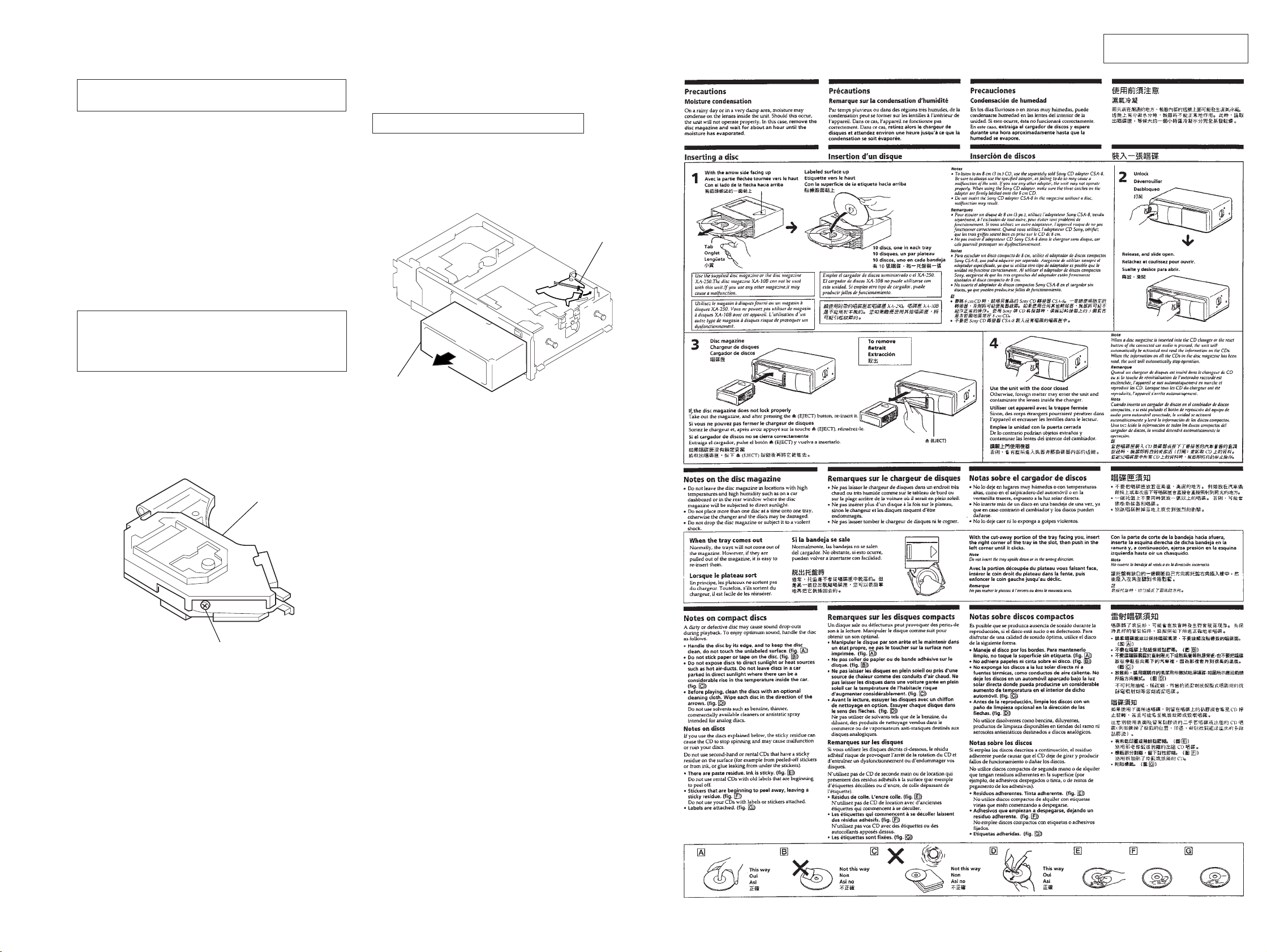
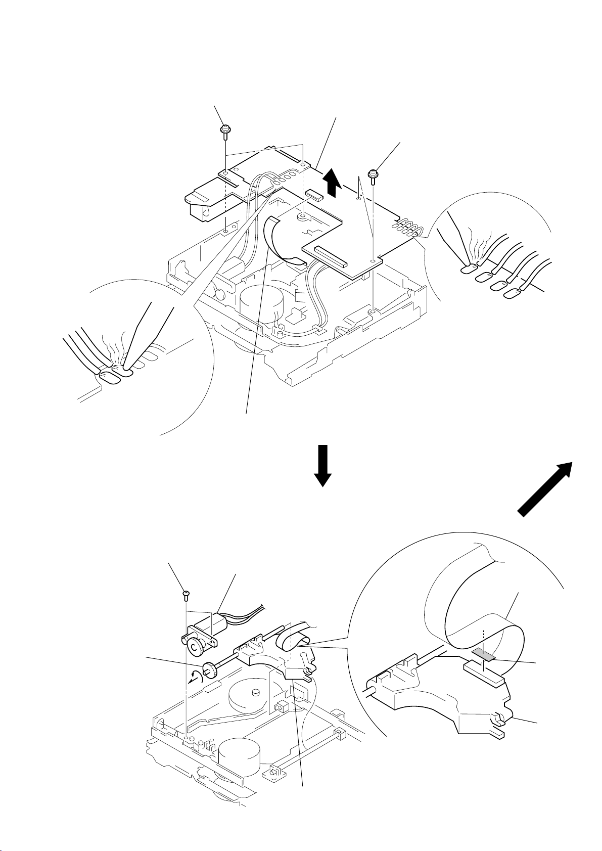
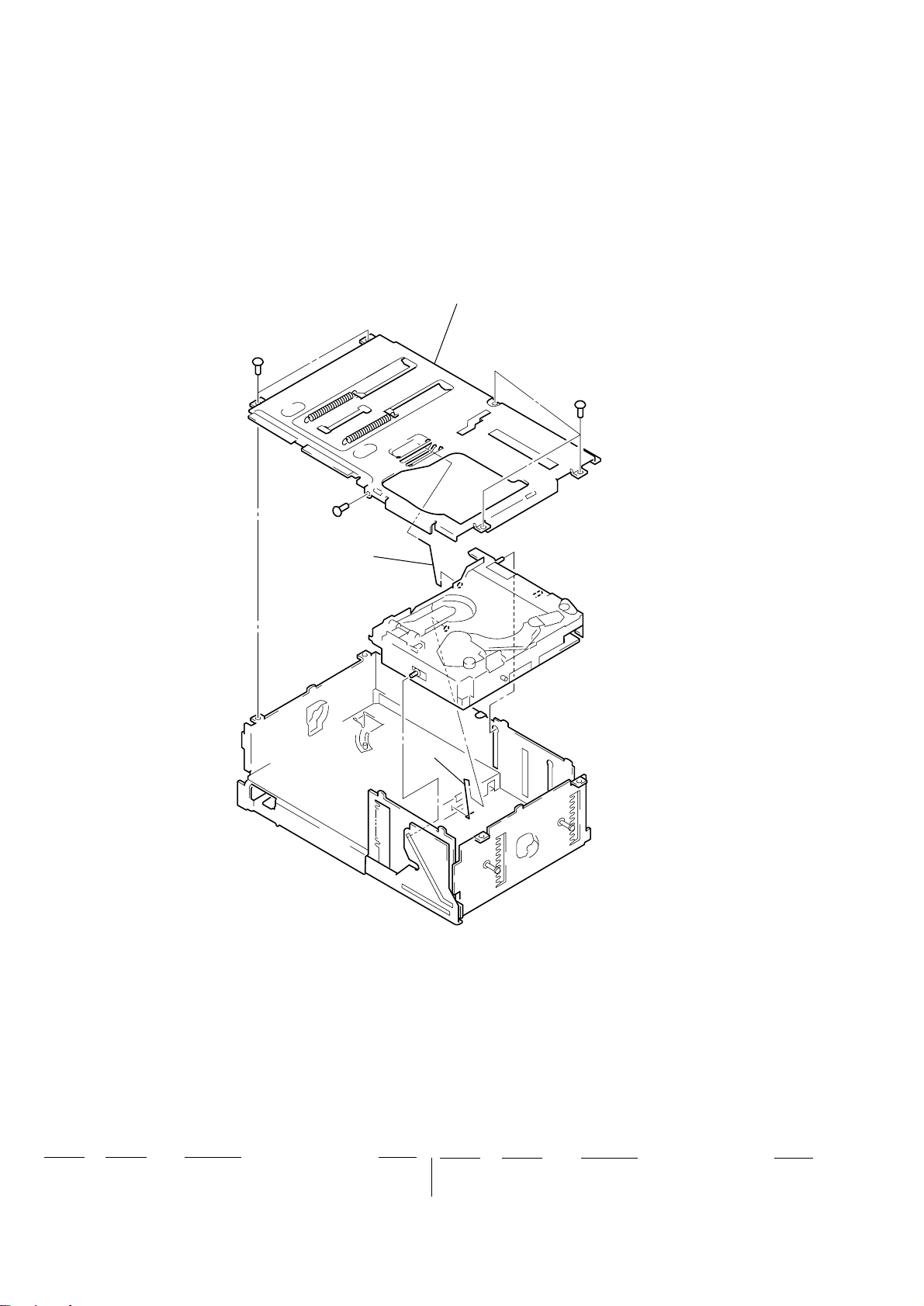
SECTION 3
)
)
DISASSEMBLY
Note: Follow the disassembly procedure in the numerical order given.
COVER (UPPER T), FRONT PANEL ASS’Y
1 screw
(PTT2.6 × 6)
3 screw
(PTT2.6 × 6)
4 lever (FLT)
3 screw (PTT2.6 × 6)
5 cover (upper T)
3 screw (PTT2.6 × 6
4 lever (FLT)
2 front panel ass’y
MECHANISM DECK (MG-251A-137)
2 tension coil spring (FL)
1 two dampers (250T)
filament tape
1 screw (PTT2.6 × 6)
4 mechanism deck (MG-251A-137)
2 tension coil spring (FL)
3 jack flexible board
(CNJ901)
1 two dampers (250T
5
Page 6

JACK BOARD
Remove the jack board of
the arrow.
1 ground point screw
(PTT2.6 × 6)
2 jack board
MAIN BOARD, SLIDE VARIABLE RESISTOR (ELEVATOR HEIGHT SENSOR) (RV202)
1 main flexible board
(CNJ101)
5 screw (FP)
2 Remove three solders of
the slide variable resistor
(RV202).
5 two screws (FP)
6 main board
2 Remove two solders of
the elevator motor leads (M104).
2 Remove two solders of
the switch board leads.
7 screw
(PTT2 × 4)
8 slide variable resistor
(elevator height sensor)
(RV202)
4 heat sink (T)
3 screw (PTT2 × 4)
6
Page 7
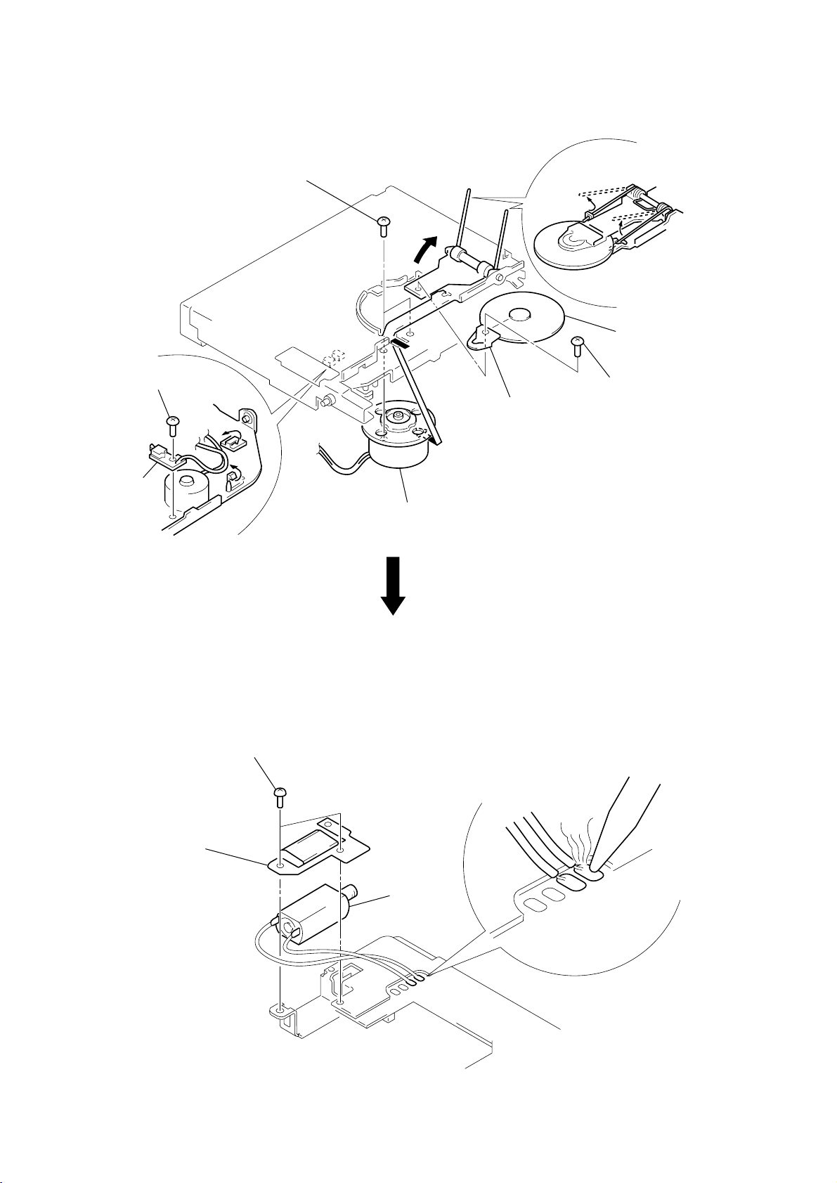
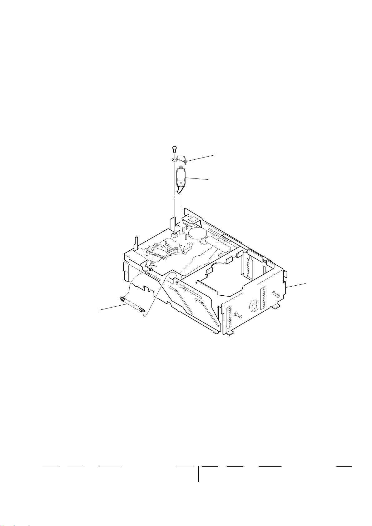
ELJ MOTOR ASS’Y (ELEVATOR) (M104)
2 bracket (EVM.S)
1 screw
(PTT2 × 4)
3 ELJ motor ass’y (elevator)
(M104)
ESCUTCHEON (T)
2 Remove the claw
in the direction of arrow A.
4 Remove the ditch
in the direction of arrow B.
5 Remove the escutcheon (T)
3 two claws
A
B
in the direction of arrow C.
3 claw
C
4 ditch
1 screw (T)
7
Page 8
CHASSIS (U.S) SUB ASS’Y
1 three screws
(PTT2 × 4)
2
3 Remove the edge
in the direction
A
of arrow A.
4 Remove the chassis (U.S)
sub ass’y in the direction
of arrow B.
CHASSIS ASS’Y
1 screw
(PTT2 × 4)
B
5 spring (SUT)
1 two screws
(PTT2 × 4)
4 Remove the chassis ass’y
5 spring (stopper.lower)
1 Turn the gear (EVD.S) fully
in the direction of arrow A.
in the direction of arrow B.
B
3
2
A
3
8
Page 9
RF BOARD
3 two screws
(PS2 × 4)
3 two screws
(PS2 × 4)
2 Remove four solders
of the LSW board leads
and spindle motor leads (M102).
2 Remove two solders
of the sled motor leads
(M101).
1 OP flexible board (CN102).
4 RF board
SLED MOTOR ASS’Y (251) (M101), OPTICAL PICK-UP (KSS-720A/K1NP)
4 Turn shaft (feed) ass’y
in the direction
of the arrow,
then remove it.
1 two precision screws
(P2 × 3)
2 sled motor ass’y (251)
(M101)
3 optical pick-up
(KSS-720A/K1NP)
OP flexible board
Note: After connecting OP flexible board,
fix it with adhesive sheet
to optical pick-up.
adhesive
sheet
optical
pick-up
9
Page 10
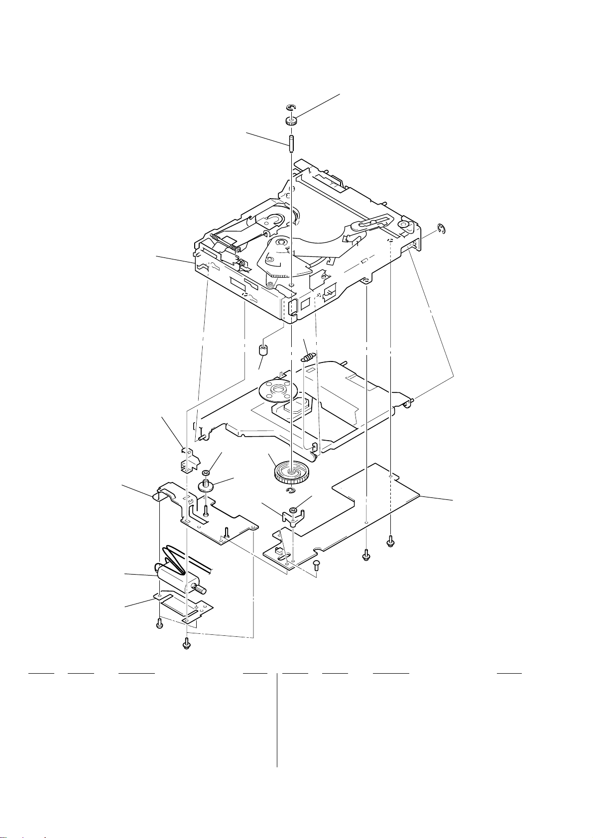
LSW BOARD, SPINDLE MOTOR (S) SUB ASS’Y (M102)
)
w
8 two precision screws
(P1.7 × 2.2)
7
3 spring (chucking)
6 retainer (disc
1 precision screw
(P2 × 2.5)
2 LSW board
ELJ MOTOR ASS’Y (CHUCKING) (M103)
2 two screws
(PTT2 × 4)
4 precision scre
5 bracket (CP)
9 Remove the spindle motor (S) sub ass’y (M102)
in the direction of the arrow.
1 Remove two solders of
the chucking motor leads (M103).
(P2 × 2.2)
10
3 retainer (CHM)
4 ELJ motor
ass’y
(chucking)
(M103)
Page 11
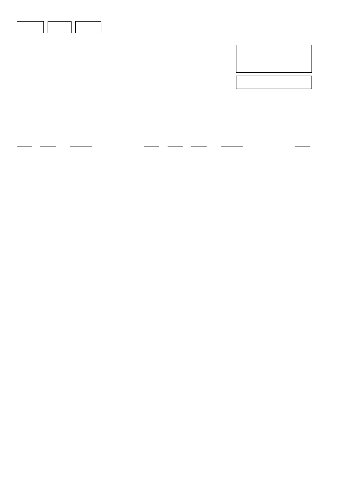
SECTION 4
)
MECHANISM DECK ASSEMBLY
Note: Follow the assembly procedure in the numerical order given.
OPTICAL PICK-UP COMPLETE ASS’Y
1 Move the lever (LOCK 3A) in the direction of arrow A,
and return it a little in the direction of arrow B
chuck plate
from the position where the chuck plate is moved
down to the lower limit.
B
A
3 stop ring 2.0 (E type
shaft (A)
GEAR (LOMINI)/(LOAD 1) ASS’Y
gear (LOAD 2)
gear (LOMINI)
chuck plate
4 tension spring (DH)
2 optical pick-up complete ass’y
Note: Insert the shaft (A) first.
2 Attach the gear (LOMINI) at the position
shown in Fig. A.
shaft (rotary prevention C)
B
1 Move the lever (LOCK 3A)
fully in the direction of arrow B
to move the chuck plate up.
marking
Fig. A
3 Attach the gear (LOAD 1) ass’y
with its facing inside.
slit
4 stop ring 1.5 (E type)
11
Page 12

OPERATION CHECK
1
Confirm that the slider moves in the direction of arrow C to move down
the chuck plate if the gear (LOAD 1) is rotated in the direction of arrow
or the chuck plate moves up and the slider mov es in the direction of arrow
D
if the gear is rotated in the direction of arrow B.
chuck plate
A
slider
D
C
A
gear (LOAD 1) ass’y
B
12
Page 13
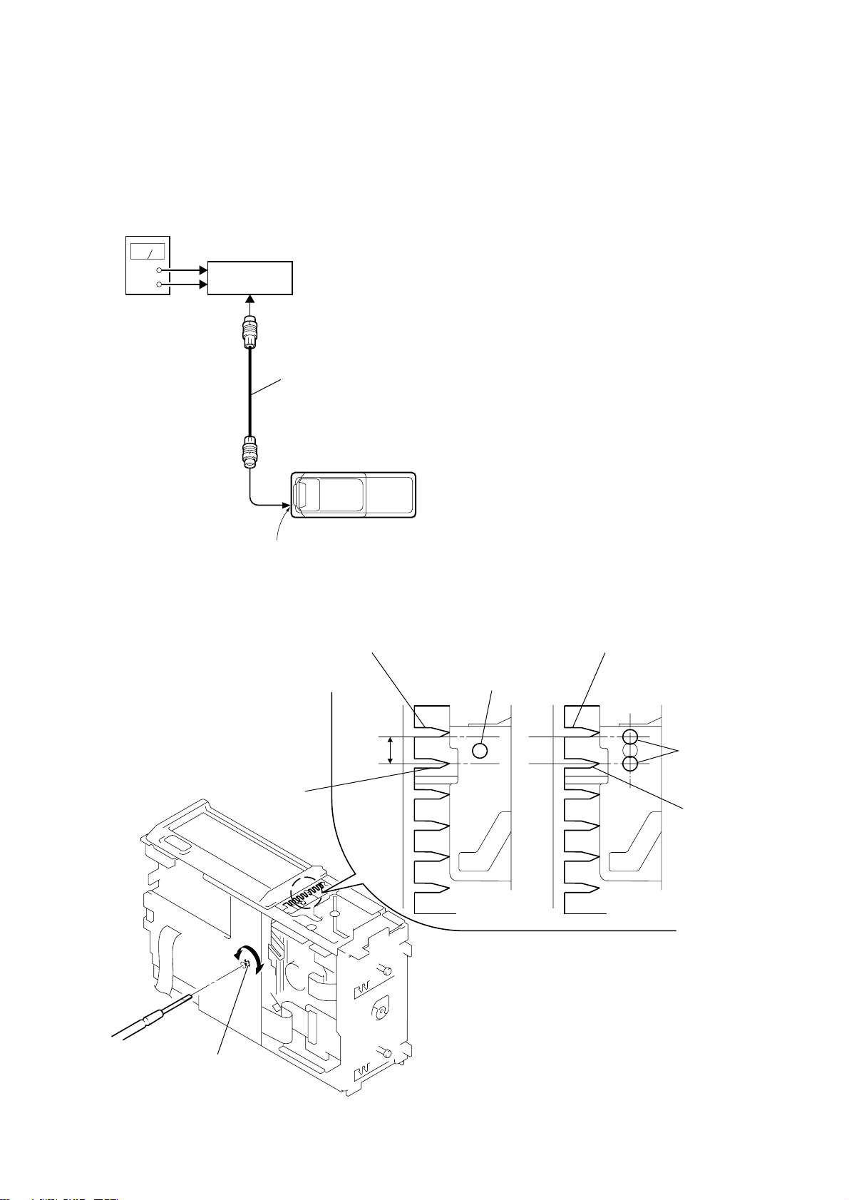
MECHANICAL ADJUSTMENT
• Elevator Height (Address) Adjustment
SECTION 5
Note: This adjustments is necessary when the system controller (IC201),
variable resistor (RV201), slider (R), slider (L), or chassis (ELV)
was replaced for any repair.
Connection:
power supply
(DC 14.4 V)
master unit
+
GND
BUS cable
compact disc changer
CONTROL connector
(CN901)
Adjustment Method:
1. Connect this set to the master unit (e.g. XR-C5300X), load a
disc magazine, and place the set vertically as shown below.
2. Connect the regulated power supply to the master unit, and
turn the power on.
3. Press the DISC button on the master unit and select DISC 5.
4. At this time, if the elevator shaft does not position between
comb teeth A and B at addresses 5 and 6 as shown below,
adjust the following.
5. Press repeatedly the DISC + and – buttons on the master unit
so that the elevator shafts moves from address 6 to address 5,
or from 5 to 6. At this time, adjust RV201 on the main board
so that the elevator shaft positions smoothly between comb
teeth A and B.
6. Further, place the set horizontally and make same adjustment
as mentioned above.
7. After adjustment at addresses 5 to 6 is finished, check all operations from addresses 1 to 10 with the set placed vertically
and horizontally respectively to confirm that the elevator shaft
positions in a range between comb teeth A to B.
comb tooth at address 6
comb tooth at address 5
comb tooth at address 6
elevator shaft
A
B
OK NG
A
elevator shaft
B
comb tooth at address 5
RV201
13
Page 14

SECTION 6
)
ELECTRICAL CHECK
Note:
1. This adjustment is performed with the set placed horizontally.
2. Power supply voltage: DC14.4 V (more than 3 A).
3. Be sure to use the disc “YEDS-18” parts code: 3-702-101-01, b ut only
when indicated.
Connection:
power supply
(DC 14.4 V)
master unit
+
GND
BUS cable
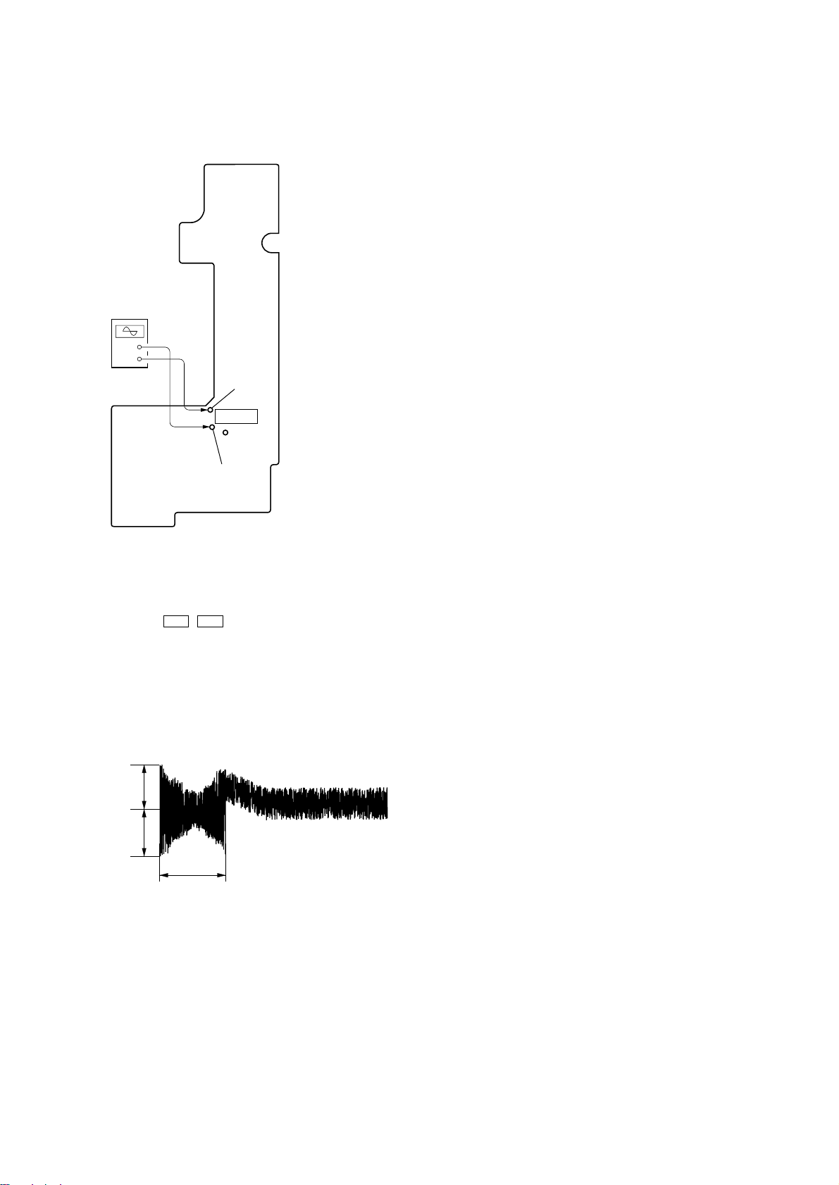
FOCUS BIAS CHECK
– RF BOARD –
(Component Side)
oscilloscope
(AC range)
+
–
TP (VC)
IC101
TP
(RFO)
compact disc changer
CONTROL connector
(CN901)
Procedure:
1. Connect the oscilloscope to TP (RFO) and TP (VC) on the RF
board.
2. Put the set into play mode by loading the disc (YEDS-18).
3. Confirm that oscilloscope waveform is clear and check RF
signal level is correct or not.
Note:
Clear RF signal waveform means that the shape “◊” can be clearly distinguished at the center of the waveform.
RF signal waveform
VOLT/DIV: 200 mV
TIME/DIV: 500 ns
(10 : 1 probe in use
level: 1.4 ± 0.3 Vp-p
When observing the eye pattern, set the oscilloscope to AC range
and raise the vertical sensitivity so that it may be easily seen.
14
Page 15
TRACKING OFFSET CHECK
– RF BOARD –
(Component Side)
oscilloscope
(DC range)
+
–
TP (VC)
IC101
TP (TE)
Procedure:
1. Connect the oscilloscope to TP (TE) and TP (VC) on the RF
board.
2. Put the set into play mode by loading the disc (YEDS-18).
3. Press the . , > buttons on the master unit, and check the
traverse waveform*.
4. Confirm that the oscilloscope waveform is symmetrical on the
top and bottom in relation to 0 V dc, and check this level.
* Traverse waveform: This is the tracking error wave form appears
when crossing the track.
Traverse waveform
A
0 V
B
A=B
traverse waveform
(100 track jump waveform)
VOLT/DIV: 500 mV
TIME/DIV: 2 ms
Center: 0 V
15
Page 16

MEMO
16
Page 17

SECTION 7
DIAGRAMS
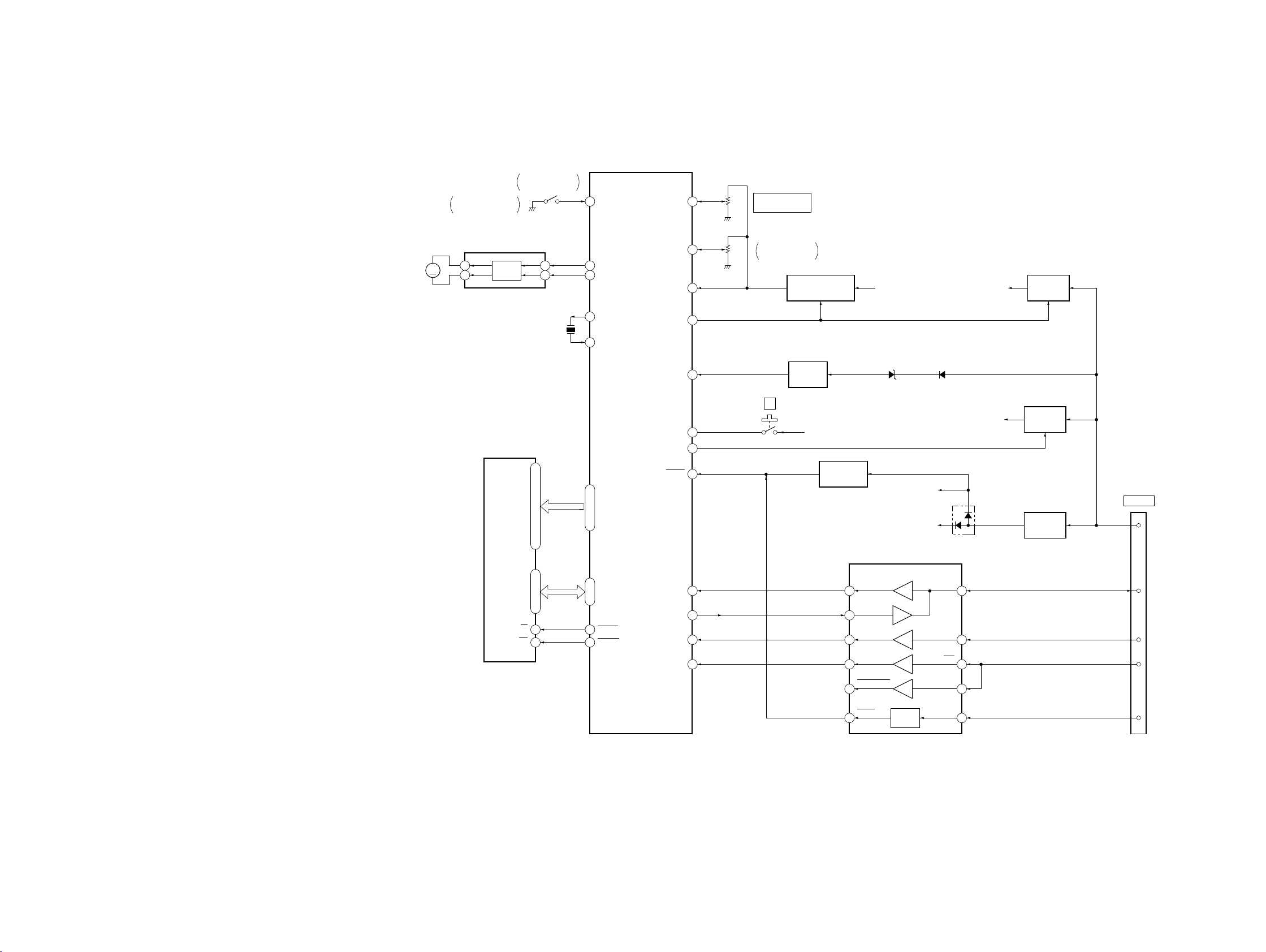
7-1. BLOCK DIAGRAM – RF SERVO/DA CONVERTER Section –
CDX-60X
FILTER
DETECTOR
PICK-UP BLOCK
(TRACKING)
(FOCUS)
05
A
B
C
D
E
F
LASER DIODE
PD LD
OPTICAL
(KSS-720A)
2-AXIS DEVICE
I-V AMP
(SPINDLE)
(CHUCKING)
M101
(SLED)
M102
M103
AUTOMATIC
POWER
CONTROL
Q101
M
M
M
FOCUS/TRACKING ERROR AMP
A
5
B
6
C
7
D
8
E
11
F
10
LD
3
TRACKING/FOCUS COIL DRIVE,
SLED/SPINDLE/CHUCKING
VO3+
8
VO3–
9
VO4+
6
VO4–
7
VO2+
10
VO2–
11
VO1+
12
VO1–
13
VL0+
5
VL0–
4
E I-V AMP
F I-V AMP
APC LD
AMP
MOTOR DRIVE
COIL
DRIVE
COIL
DRIVE
MOTOR
DRIVE
MOTOR
DRIVE
MOTOR
DRIVE
SUMMING
IC201
AMP
FOCUS
ERROR
RF AMP,
IC101
RF
AMP
APC PD
AMP
VIN3+
VIN3–
VIN4+
VIN4–
VIN2+
VIN2–
VIN1–B
FWD
REV
RF EQ
AMP
TRACKING
ERROR
AMP
AGC
25
24
31
32
22
21
18
1
2
RFO
LDON
HOLD SW
AGCCONT
L
R
CN901 (1/2)
ANALOG OUT
L
R
63 66 6564
FILI
PCO
FILO
CLTV
RFAC
ASYI
ASYO
DIGITAL SERVO
CLV
ASYMMENTRY
CORRECTOR
RFDC
FE
TE
54 50 52 51
ANALOG SWITCH
A/D CONVERTER
SIGNAL PROCESS
ON : When the optical pick-up
is inner position
16
FE
14
TE
13
22
21
20
PD
4
TEDR
40
TRDR
41
FFDR
42
FRDR
43
SFDR
38
SRDR
39
MDP
35
61
60
59
LDON
HOLD
AGC
PWM GENERATOR
DIGITAL
RFDC
RFDC
OP AMP
DIGITAL
PLL
FE
TE
FE
TE
SE
MIRR
DFCT
FOK
83
EMPH
EFM
DE-
MODULATOR
SUBCODE
PROCESS
SW3
(LIMIT)
D/A
INTER-
FACE
32k RAM
INTERNAL BUS
CORRECTOR
PCMD
LRCK
BCK
ERROR
CPU
INTERFACE
SERVO AUTO
SEQUENCER
SERVO
INTERFACE
SSTP
36
EMPHI
84
79
77
81
GFS
DATA
CLOK
XLAT
SENS
SQSO
SQCK
SCOR
SCLK
FOK
XRST
80
78
82
22
13
15
14
16
6
7
24
17
32
11
SERIAL
PCMDI
LRCKI
BCKI
IN
INTERFACE
DIGITAL SIGNAL PROCESSOR,
DIGITAL FILTER, D/A CONVERTER,
DIGITAL SERVO PROCESSOR
IC101
DIGITAL FILTER,
NOISE SHAPER
LDON
HOLD
AGC
54
55
56
91
6
7
5
93
77
79
82
92
90
94
INTEGRATOR
LDON
AGCHOLD
RF AGC
GFS
CDDATA
CDCLK
CDXLT
SENS
SQSO
SQCK
SCOR
SCLK
FOK
XRST
AOUT2
PWM
&
AOUT1
SYSTEM CONTROLLER
IC201 (1/2)
97
90
CLOCK
GENERATOR
AMUTE
BUFFER
TIMING
LOGIC
LOUT
ROUT
XTAO
XTAI
92
95
87
86
GND-ISOLATION
16.9344MHz
MUTING
CONTROL
Q401, 402
X130
IC401
MUTING
Q410, 420
AIN2
96
AIN1
91
4
• SIGNAL PATH
: CD PLAY
CH. F
71
CH. R
72
LIMSW
89
ON : When completion of the disc
save operation
ON : When completion of the disc
chucking operation
SW1
(SAVE END DETECT)
SW2
(CHUCKING END DETECT)
LOAD1
65
LOAD2
66
1717
Page 18
CDX-60X
7-2. BLOCK DIAGRAM – BUS CONTROL/POWER SUPPLY Section –
SYSTEM CONTROLLER
ON : When magazine
is set
SW201
MAGAZINE IN/OUT
DETECT
76
MGLK
IC201 (2/2)
MCK
60
RV201
ELEVATOR HEIGHT
(ADDRESS)
M104
(ELEVATOR)
ELEVATOR
MOTOR DRIVE
IC301
OUT1
9
M
OUT2
7
MOTOR
DRIVE
S-RAM
IC202
IN1
IN2
A0–A14
10–3, 25, 24, 21, 23, 2, 26, 111–13, 15–19
3
4
X201
12MHz
ELVF
74
73
ELVR
40
XTAL
41
EXTAL
28–21, 36–3020–13
RAMA0–RAMA14RAMIO1–RAMIO8
EHS
VREF
ELVON
BUCHK
EJECT
CDON
RESET
59
51
9
75
63
8
38
RV202
ELEVATOR HEIGHT
SENSOR
REFERENCE VOLTAGE
BATTERY
CHECK
SW801
Q301, 302
Z
SWITCH
Q201
B. UP +5V
RESET SIGNAL
GENERATOR
IC303
B. UP +5V
D306
B. UP +5V
BUS +5V
BUS INTERFACE
(FOR SONY BUS)
IC302
D307
DRIVER +8V
DAC/SERVO +5V
D308
+8V
REGULATOR
IC304
+5V
REGURATOR
IC305
+5V
REGURATOR
Q303
CN901 (2/2)
CONTROL
7
B. UP
SO
43
SI
DO0–DO7
SO
44
20
CE
WE
27
05
37
12
RAMCE
RAMWE
SCLK
BUSON
45
62
10 6
SI
9
SCK
11 4
BUSON OUT
1 12
BUSON OUT
13 2
RESET
8 7
RESET
SWITCH
DATA
CLK
LOF
BUSON IN
RST
5
DATA
4
CLK
6
BUSON
2
RST
1818
Page 19

• Circuit Boards Location
d
7-3. NOTE FOR PRINTED WIRING BOARDS AND SCHEMATIC DIAGRAMS
SWITCH board
JACK board
LSW board
MAIN board
RF boar
Note on Printed Wiring Boards:
• X : parts extracted from the component side.
• Y : parts extracted from the conductor side.
f
•
: internal component.
• b : Pattern from the side which enables seeing.
(The other layers' patterns are not indicated.)
Caution:
Pattern face side: Parts on the pattern face side seen from
(Conductor Side) the pattern face are indicated.
Parts face side: Parts on the parts face side seen from
(Component Side) the parts face are indicated.
Note on Schematic Diagram:
• All capacitors are in µF unless otherwise noted. pF: µµF
50 WV or less are not indicated except for electrolytics
and tantalums.
• All resistors are in Ω and 1/
specified.
f
•
: internal component.
4
W or less unless otherwise
• C : panel designation.
Note: The components identified by mark 0 or dotted line
with mark 0 are critical for safety.
Replace only with part number specified.
• U : B+ Line.
• H : adjustment for repair.
• Power voltage is dc 14.4V and fed with regulated dc power
supply from CD changer controller.
• Voltages and waveforms are dc with respect to ground
under no-signal conditions.
no mark : CD PLAY
: Impossible to measure
∗
• Voltages are tak en with a V OM (Input impedance 10 MΩ).
Voltage variations may be noted due to normal production tolerances.
• Waveforms are taken with a oscilloscope.
Voltage variations may be noted due to normal production tolerances.
• Circled numbers refer to waveforms.
• Signal path.
J : CD PLAY
1919
Page 20

CDX-60X
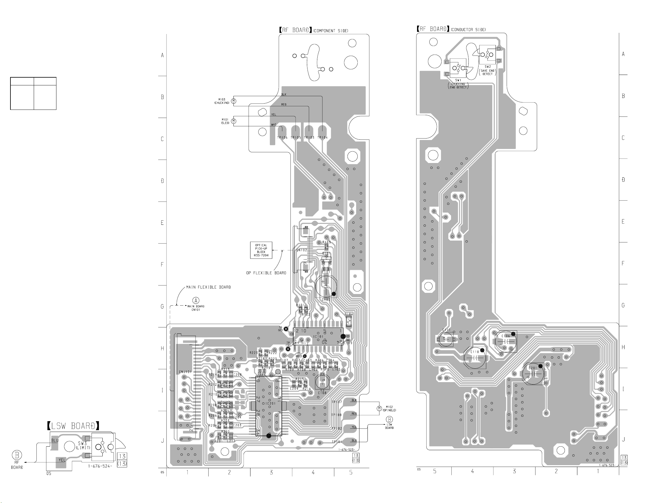
7-4. PRINTED WIRING BOARDS – RF/LSW Boards – • See page 19 for Circuit Boards Location.
• Semiconductor
Location
(Component Side)
Ref. No. Location
IC101 H-4
IC201 I-3
Q101 F-5
(Page 22)
2020
Page 21
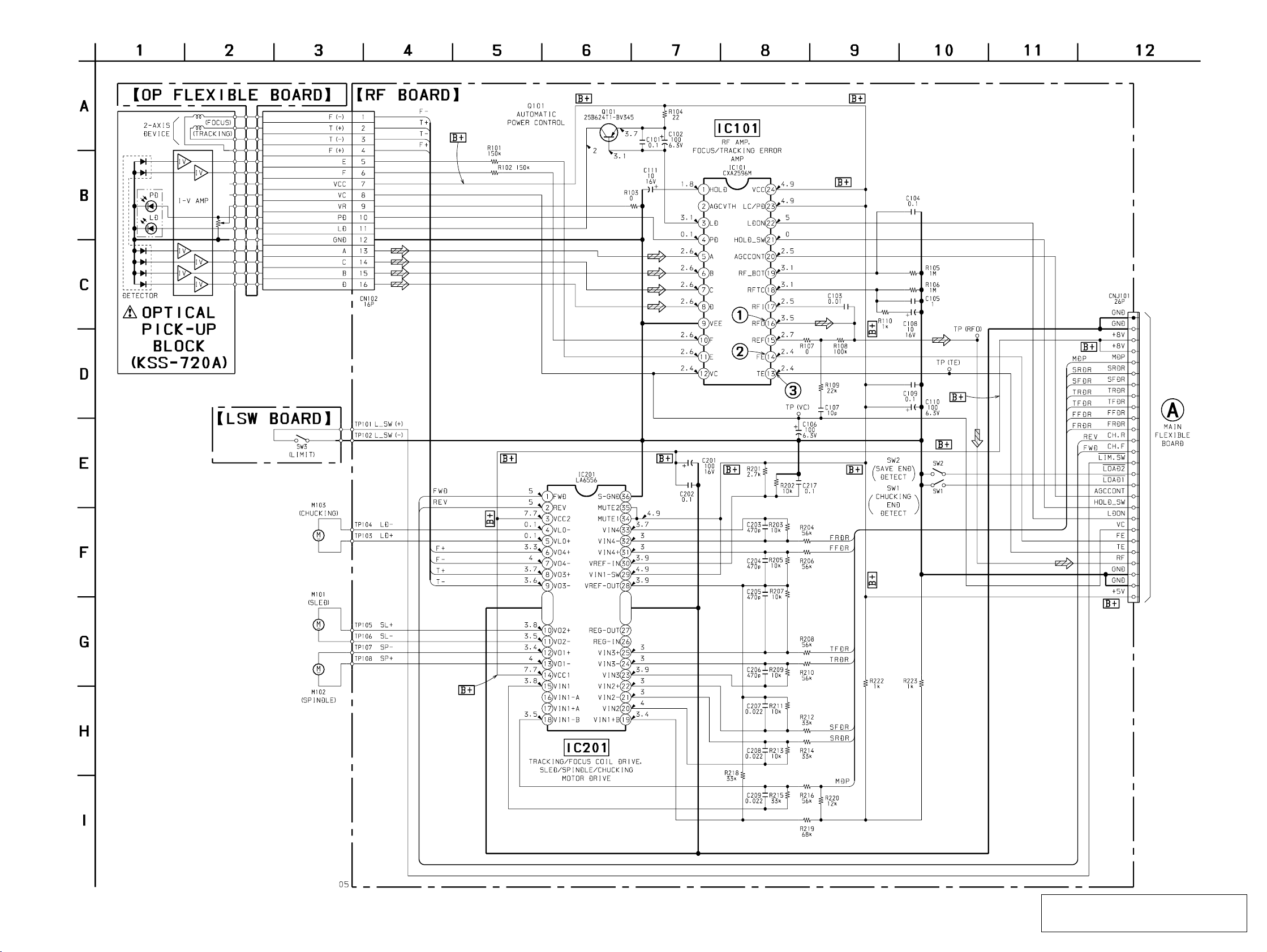
7-5. SCHEMATIC DIAGRAM – RF/LSW Boards – • See page 27 for for Waveforms. • See page 28 for IC Block Diagrams.
CDX-60X
(Page 24)
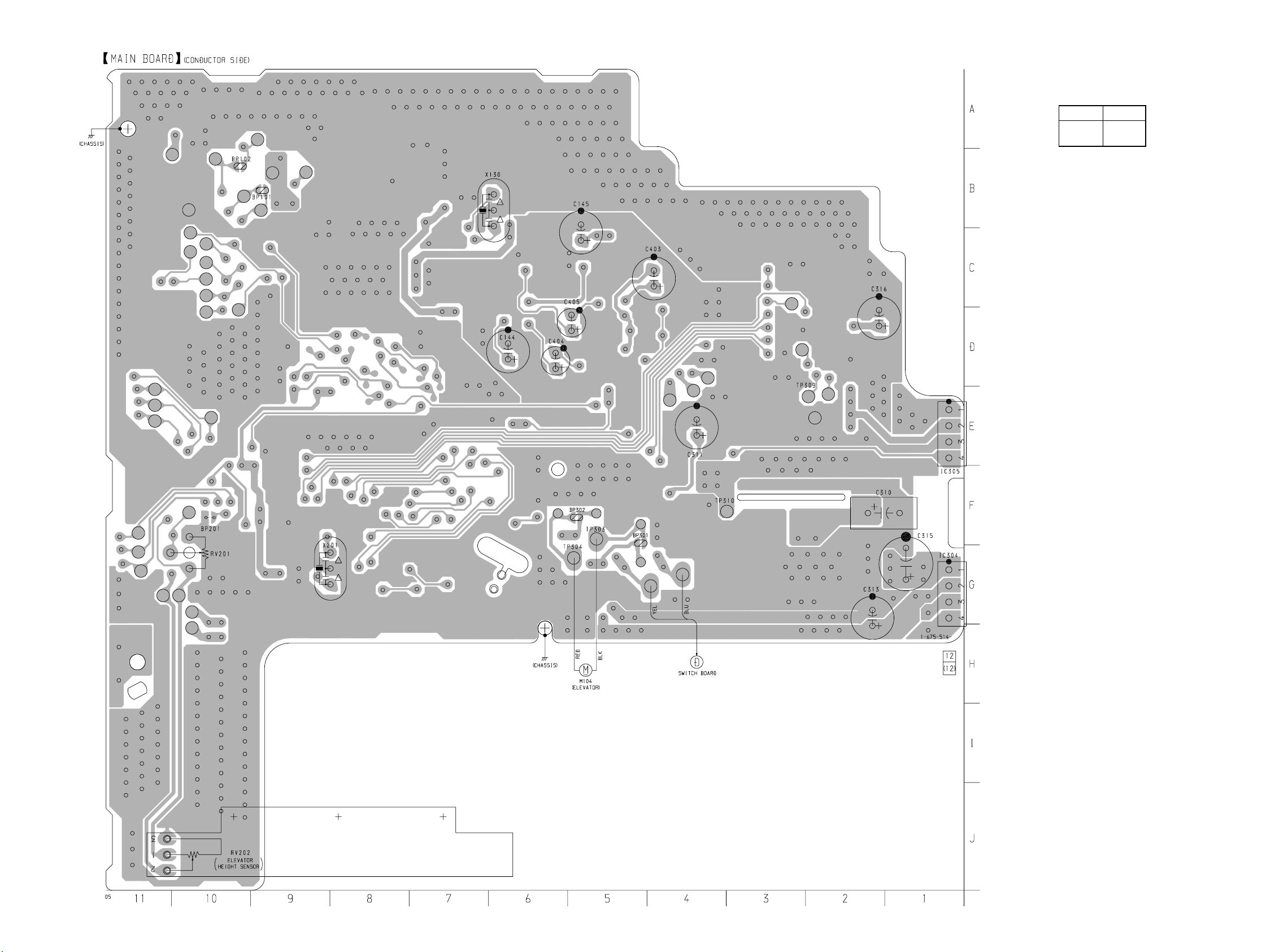
The components identified by mark 0 or dotted
line with mark 0 are critical for safety.
2121
Replace only with part number specified.
Page 22
CDX-60X
7-6. PRINTED WIRING BOARDS – MAIN Board (Component Side) – • See page 19 for Circuit Boards Location.
• Semiconductor
Location
Ref. No. Location
D301 D-2
D302 D-2
D303 D-3
D304 D-3
D305 D-3
D306 F-4
D307 F-4
D308 G-4
D309 F-4
D310 F-3
D311 F-2
D312 G-3
IC101 C-8
IC201 F-8
IC202 F-7
IC301 G-3
IC302 D-2
IC303 F-3
IC401 C-6
(Page 20)
Q201 E-10
Q301 F-5
Q302 F-5
Q303 F-4
Q401 D-5
Q402 D-5
Q410 D-5
Q420 D-5
(Page 26)
2222
Page 23
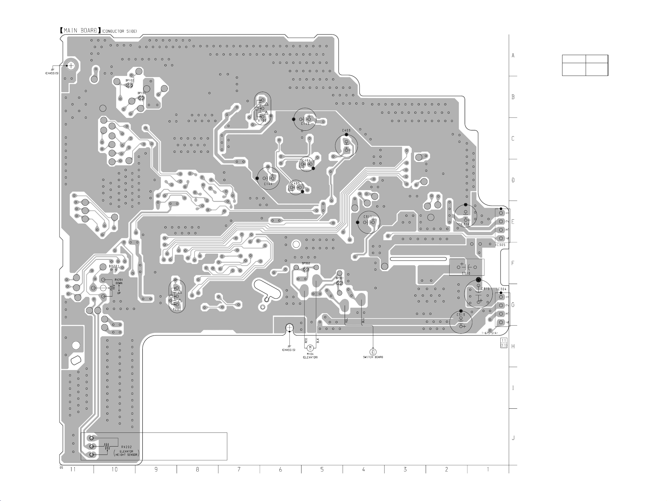
7-7. PRINTED WIRING BOARD – MAIN Board (Conductor Side) – • See page 19 for Circuit Boards Location.
CDX-60X
• Semiconductor
Location
Ref. No. Location
IC304 G-1
IC305 E-1
(Page 26)
2323
Page 24

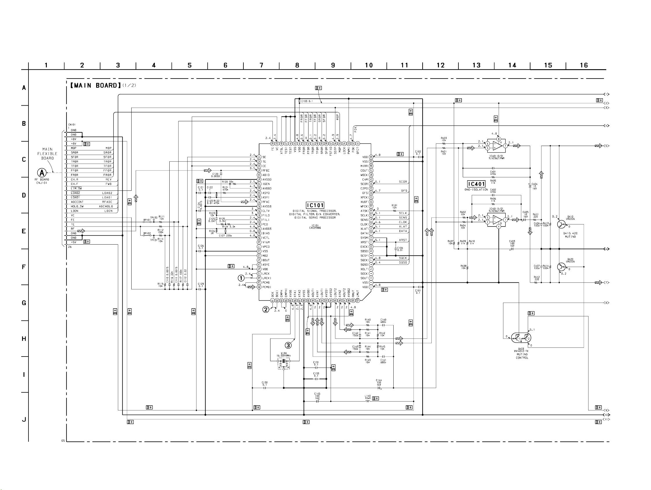
CDX-60X
7-8. SCHEMATIC DIAGRAM – MAIN Board (1/2) – • See page 27 for Waveforms. • See page 28 for IC Block Diagram.
(Page 21)
2424
Page 25

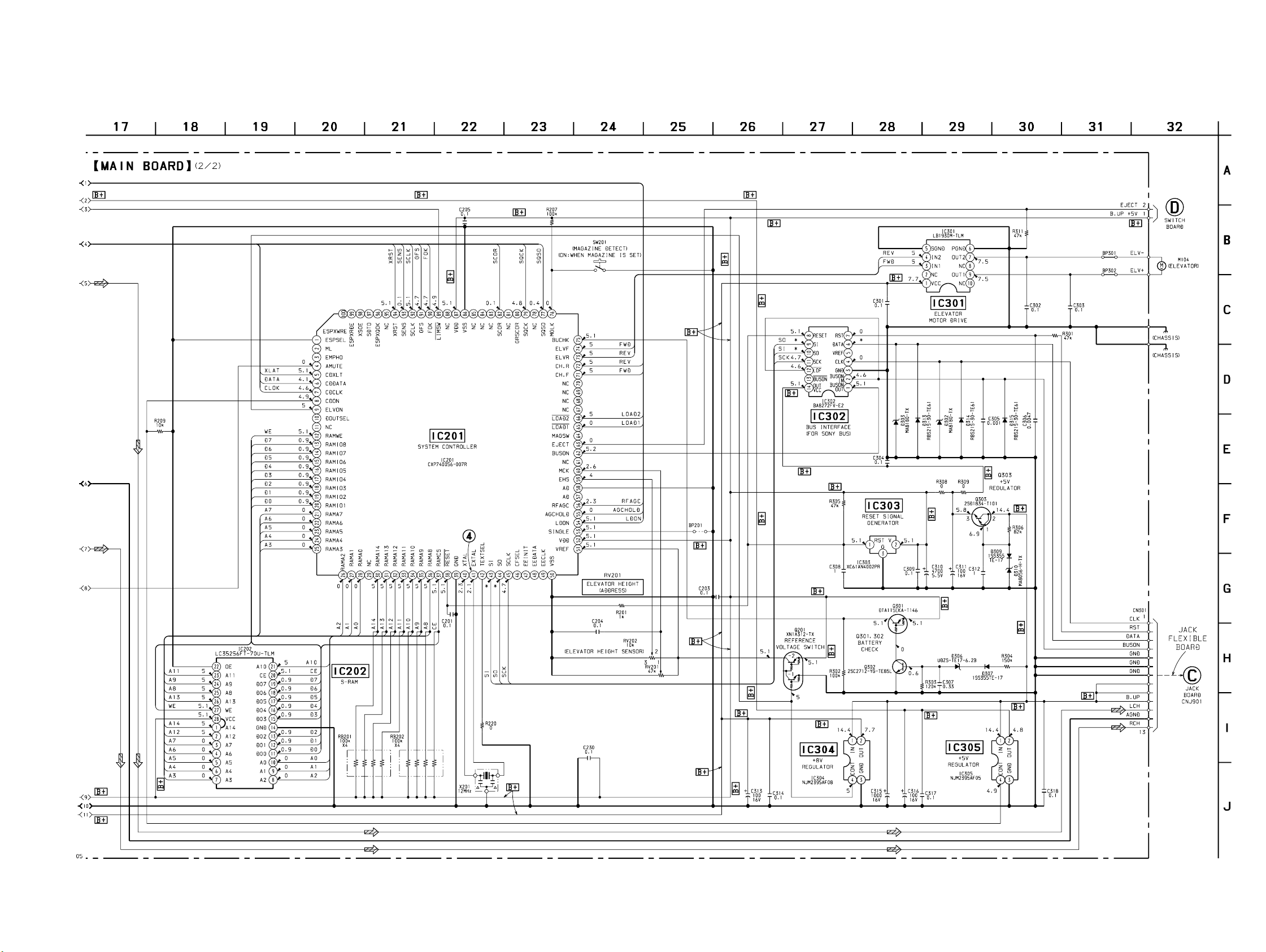
7-9. SCHEMATIC DIAGRAM – MAIN Board (2/2) – • See page 27 for Waveform. • See page 28 for IC Block Diagrams.
CDX-60X
(Page 26)
(Page
26)
2525
Page 26

CDX-60X
7-10. PRINTED WIRING BOARDS – JACK/SWITCH Boards –
• See page 19 for Circuit Boards Location.
(Page 22)
7-11. SCHEMATIC DIAGRAM – JACK/SWITCH Boards –
(Page 25)
(Page 23)
(Page 25)
2626
Page 27

• Waveforms
– RF Board –
– MAIN Board –
1 IC101 qh (RFO) (play mode)
2 IC101 qf (FE) (play mode)
3 IC101 qd (TE) (play mode)
1.4 ± 0.3
Vp-p
Apporx.
63 mVp-p
1 IC101 uj (LRCK), uk (LRCKI)
(play mode)
5.6 Vp-p
22.8 µs
2 IC101 ia (BCK), is (BCKI)
(play mode)
5.7 Vp-p
470 ns
3 IC101 ih (XTAI) (play mode)
Approx.
63 mVp-p
4.1 Vp-p
60 ns
4 IC201 ra (EXTAL) (play mode)
4.4 Vp-p
83 ns
27
Page 28

• IC Block Diagrams
– RF Board –
IC101 CXA2596M-T6
1
HOLD
2
AGCVTH
3
LD
4
PD
APC LD
AMP
APC PD
AMP
AGC
24 VCC
23
LC/PD
22
LD ON
21
HOLD SW
20
AGCCONT
VEE
COMPARATOR
COMPARATOR
5
A
6
B
7
C
8
D
9
10
F
11
E
12
VC
VCC
VEE
RF SUMMING
AMP
FOCUS ERROR
AMP
F I-V AMP
E I-V AMP
RF EQ
AMP
TRACKING
ERROR
AMP
19
RF BOT
18
RFTC
17
RF I
16
RFO
15
RFE
14
FE
13
TE
28
Page 29

IC201 LA6556L-TE-L
FWD
REV
VCC2
VLO–
VLO+
VO4+
VO4–
VO3+
VO3–
VO2+
VO2–
VO1+
VO1–
OUTPUT
CONTROL
LEVEL
SHIFT
LEVEL
SHIFT
–
+
LEVEL
SHIFT
LEVEL
SHIFT
THERMAL SHUT DOWN
–
+
–
+
5VREG
+
–
CH2-4
MUTE
CH1
MUTE
VIN1/VREF
SWITCH
1
INPUT
2
3
4
5
6
7
8
9
10
11
12
13
–
+
–
+
+
–
S-GND
36
35
MUTE2
34
MUTE1
33
VIN4
32
VIN4–
31
VIN4+
30
VREF-IN
29
VIN1 (VREF)-SW
28
VREF-OUT (CH1)
27
REG-OUT
REG-IN
26
25
VIN3+
VIN3–
24
VCC1
VIN1
VIN1–A
VIN1+A
VIN1–B
14
15
16
–
AMP-A
+
17
–
18
AMP-B
+
–
+
–
+
VIN3
23
22
VIN2+
+
–
21
VIN2–
VIN2
20
VIN1+B
19
29
Page 30

– MAIN Board –
IC101 CXD2598Q
81
BCK
BCKI
82
ENPH
83
EMPHI
84
XVDD
85
XTAI
86
TIMING
87
88
89
90
91
92
93
94
95
96
97
LOGIC
LOW-PASS
FILTER
–
+
+
–
LOW-PASS
FILTER
OVER SAMPLING
DIGITAL FILTER
NOISE SHAPER
VC
VC
XTAO
XVSS
AVDD1
AOUT1
AIN1
LOUT1
AVSS1
AVSS2
LOUT2
AIN2
AOUT2
PCMDI
PCMD
LRCKI
LRCK
VDD
80
79 78 77 76 75 74 73 72 71 70 69 68 67 66 65 64 63 62 61 60 59 58 57 56 55
SERIAL-IN
INTERFACE
3rd-ORDER
PWM
PWM
SERVO
INTERFACE
ASYE
D/A
INTERFACE
INTERNAL BUS
32k
RAM
DOUT
MD2
DIGITAL
OUT
ERROR
CORRECTOR
SERVO
AUTO
SEQUENCER
VSS
VPCO
V16M
CLOCK
GENERATOR
DEMODULATOR
SUB CODE
PROCESSOR
VCTL
EFM
BIAS
AVDD3
PCO
FILI
DIGITAL
PLL
FILO
CLTV
ASYMMETRY
CORRECTOR
AVSS3
RFAC
ASYI
ASYO
AVDD0
A/D
CONVERTER
SERVO DSP
FOCUS SERVO
TRACKING
SERVO
SLED SERVO
MIRR
DFCT
FOK
IGEN
AVSS0
ADIO
OP AMP
ANALOG
SWITCH
PWM GENERATOR
RFDCCETE
54 53 52 51
FOCUS PWM
GENERATOR
TRACKING PWM
GENERATOR
SLED PWM
GENERATOR
DIGITAL
CLV
SE
50
FE
VC
49
XTSL
48
TES1
47
TEST
46
VSS
45
VDD
44
FRDR
43
FFDR
42
TRDR
41
TFDR
40
SRDR
39
SFDR
38
FSTIO
37
SSTP
36
MDP
35
LOCK
34
PWMI
33
FOK
32
DFCT
31
AVDD2
RMUT
LMUT
98
99
100
VSS
VDD
SOUT
SOCK
XOLT
SQSO
SQCK
SCSY
INTERFACE
EXCK
SBSO
CPU
XRST
SYSM
DATA
XLAT
CLOK
SENS
SCKL
ATSK
WFCK
XUGF
XPCK
GFS
C2PO
SCOR
C4M
WDCK
COUT
MIRR
VSS
302928272625242322212019181716151413121110987654321
VDD
30
Page 31

IC202 LC35256FT-70U-TLM
A11
A13
VCC
A14
A12
ADDRESS
OE
22
23
24
A9
25
A8
26
27
WE
28
1
2
3
A7
4
A6
5
A5
6
A4
7
A3
BUFFER
INPUT
DATA
BUFFER
ROW
DECODER
INPUT
DATA
CONTROL
MEMORY
CELL ARRAY
512 x 512
COLUMN
I/O
CONTROL
COLUMN
DECODER
ADDRESS
BUFFER
OUTPUT
DATA
BUFFER
21
A10
20
CE
19
I/O8
18
I/O7
17
I/O6
16
I/O5
15
I/O4
14
GND
13
I/O3
12
I/O2
11
I/O1
10
A0
9
A1
8
A2
IC301 LB1930M-TLM IC304 NJM2395F08
IC302 BA8272F-E2
IC305 NJM2395F05
NC
VCC
S-GND
IN1
IN2
1
BUFFER
NC
2
3
4
BUFFER
5
CONTROL
CIRCUIT
MOTOR
DRIVE
CIRCUIT
10
9
8
7
6
OUT1
NC
OUT2
P-GND
VCC
BUS ON
14 13 12
2 3
1
BUS ON IN
BUS ON OUT
LINK OFF
CLK OUT
11
5 6 7
4
GND
VREF
BUS CLK
DATA OUT
10
BUS DATA
DATA IN
RESET
89
RESET
SWITCH
BUS RESET
CONTROL
2
VOUT
3
GND
1
VIN
4
CONT
31
Page 32
7-12. IC PIN FUNCTION DESCRIPTION
• MAIN BOARD IC201 CXP740056-007R (SYSTEM CONTROLLER)
Pin No. Pin Name I/O Description
1 ESPSEL I ESP on/off setting terminal “L”: ESP on Not used (open)
2MLO
3 EMPHO O Emphasis signal output terminal Not used (open)
4 AMUTE O Audio line muting on/off control signal output terminal “H”: muting on
5 CDXLT O Serial data latch pulse signal output to the CXD2598Q (IC101)
6 CDDATA O Serial data output to the CXD2598Q (IC101)
7 CDCLK O Serial data transfer clock signal output to the CXD2598Q (IC101)
8 CDON O D/A converter and servo section power supply on/off control signal output “H”: power on
9 ELVON O Mechanism deck section power supply on/off control signal output “H”: power on
10 DOUTSEL I Digital output on/off control signal input terminal “L”: digital output on Not used (open)
11 NC — Not used (open)
12 RAMWE O Data write enable signal output to the S-RAM (IC202) “L”: active
13 to 20
21 to 28 RAM7 to RAM0 O Address signal output to the S-RAM (IC202)
29 NC — Not used (open)
30 to 36
37 RAMCE O Chip enable signal output to the S-RAM (IC202) “L”: active
38 RESET I
39 GND — Ground terminal
40 XTAL O Main system clock output terminal (12 MHz)
41 EXTAL I Main system clock input terminal (12 MHz)
42 TEXTSEL I
43 SI I Serial data input from the SONY bus interface (IC302)
44 SO O Serial data output to the SONY bus interface (IC302)
45 SCLK I Serial data transfer clock signal input from the SONY bus interface (IC302)
46 CFSEL I Custom file on/off setting terminal “L” custom file on Fixed at “H” (open)
47 EEINIT I Initialize signal input for the EEPROM “H”: format Not used (open)
48 EEDATA I/O Two-way data bus with the EEPROM Not used (open)
49 EECLK O Serial data transfer clock signal output to the EEPROM Not used (open)
50 VSS — Ground terminal (for A/D converter)
51 AVREF I Reference voltage (+5V) input terminal (for A/D converter)
52 VDD — Power supply terminal (+5V) (for A/D converter)
53 SINGLE I
54 LDON O The laser automatic power control on/off signal output “H”: automatic power control on
55 AGCHOLD O RF AGC hold on/off signal output “H”: hold
56 RFAGC I/O RF AGC level control signal output “L”: off, center voltage: 40%, “H”: 60%
57 AD I A/D input terminal Not used (fixed at “L”)
58 AD I A/D input terminal Not used (open)
59 EHS I Elevator height position detect input from the RV202 (elevator height sensor) (A/D input)
RAMIO8 to
RAMIO1
RAM14 to
RAM8
Normal/high speed playback control signal output terminal “L”: high speed playback
Not used (open)
I/O Two-way data bus with the S-RAM (IC202)
O Address signal output to the S-RAM (IC202)
System reset signal input from the SONY bus interface (IC302) and reset signal generator (IC303)
“L”: reset
For several hundreds msec. after the power supply rises, “L” is input, then it changes to “H”
CD text mode setting terminal “L”: CD text on, “H”: does not display track name
Fixed at “L” in this set
Setting terminal for the single disc/multiple discs mode
“L”: single mode, “H”: multiple discs mode Fixed at “H” in this set (open)
32
Page 33

Pin No. Pin Name I/O Description
60 MCK I
61 NC — Not used (open)
62 BUSON I Bus on/off control signal input from the SONY bus interface (IC302) “H” bus on
63 EJECT I Eject switch (SW801) input terminal “H” active
64 MAGSW I Magazine in/out detect switch input Not used (open)
65 LOAD1 I
66 LOAD2 I
67 to 70 NC — Not used (open)
71 CH.F O
72 CH.R O
73 ELVR O
74 ELVF O
75 BUCHK I Battery detect signal input terminal “H”: battery on
76 MGLK I Magazine in/out detect switch (SW201) input “L”: magazine is set
77 SQSO O Subcode Q/text serial data output to the CXD2598Q (IC101)
78 NC — Not used (open)
79 SQCK O Subcode Q/text serial data transfer clock signal output to the CXD2598Q (IC101)
80 GRSCOR I Subcode sync (S0+S1) detection signal input terminal Not used (open)
81 NC — Not used (open)
82 SCOR I Subcode sync (S0+S1) detection signal input from the CXD2598Q (IC101)
83 SIRCS I SIRCS signal input terminal Not used (open)
84 TEX I Sub system clock input terminal Not used (open)
85 TX O Sub system clock output terminal Not used (open)
86 VSS — Ground terminal
87 VDD — Power supply terminal (+5V)
88 NC — Not used (open)
Input of signal for the fine adjustment (elvator height (address) adjustment; RV201) of elevator
position (A/D input)
Chucking end detect switch (SW1) input terminal
“L”: When completion of the disc chucking operation
Save end detect switch (SW2) input terminal
“L”: When completion of the disc save operation
Motor drive signal (save direction) output to the chucking motor drive (IC201)
“L” active *1
Motor drive signal (chucking direction) output to the chucking motor drive (IC201)
“L” active *1
Motor drive signal (elevator down direction) output to the elevator motor drive (IC301)
“L” active *2
Motor drive signal (elevator up direction) output to the elevator motor drive (IC301)
“L” active *2
*1 chucking motor (M103) control
Terminal
Mode
CH.F (pin ua) “H”“H”“L”“L”
CH.R (pin us) “H”“L”“H”“L”
*2 elevator motor (M104) control
Mode
Terminal
ELVF (pin uf) “H”“L”“H”“L”
ELVR (pin ud) “H”“H”“L”“L”
STOP
STOP
LOAD
CHUCKING
ELEVATOR UPELEVATOR
SAVE BRAKE
DOWN
BRAKE
33
Page 34
Pin No. Pin Name I/O Description
89 LIMSW I
90 FOK I Focus OK signal input from the CXD2598Q (IC101) “H” is input when focus is on (“L”: NG)
91 GFS I Guard frame sync signal input from the CXD2598Q (IC101) “L”: NG, “H”: OK
92 SCLK O Serial data transfer clock signal output to the CXD2598Q (IC101)
93 SENS I Internal status signal (sense signal) input from the CXD2598Q (IC101)
94 XRST O System reset signal output to the CXD2598Q (IC101) “L”: reset
95 NC — Not used (open)
96 ESPXQOK O Subcode Q OK pulse signal output terminal “L”: active Not used (open)
97 SDTO I ESP status signal input terminal Not used (open)
98 XSOE O ESP status read enable signal output terminal “L”: active Not used (open)
99 ESPXRED O ESP read enable signal output terminal “L”: active Not used (open)
100 ESPXWRE O ESP write enable signal output terminal “L”: active Not used (open)
Sled limit in detect switch (SW3) input terminal
“L”: When the optical pick-up is inner position
34
Page 35
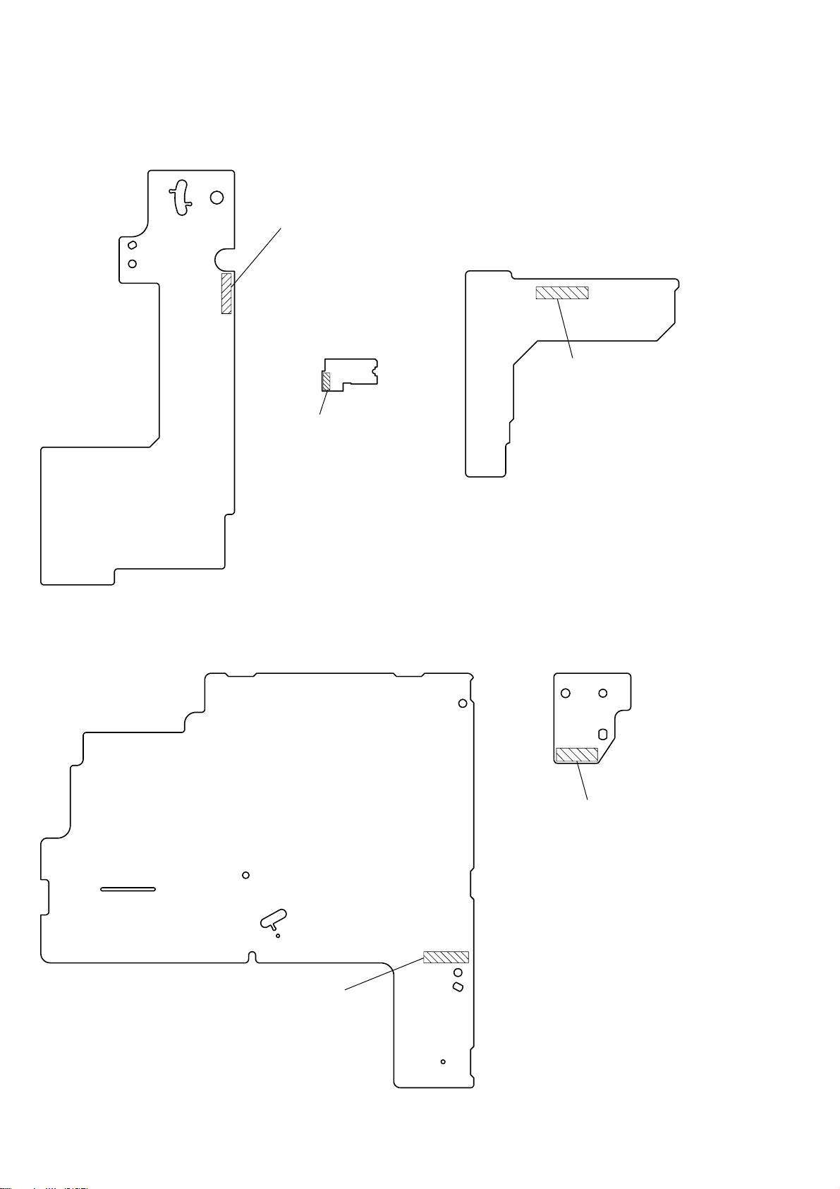
SECTION 8
7
EXPLODED VIEWS
NOTE:
• -XX and -X mean standardized parts, so they
may have some difference from the original
one.
• Color Indication of Appearance Parts
Example:
KNOB, BALANCE (WHITE) . . . (RED)
↑↑
Parts Color Cabinet's Color
(1) COVER SECTION
13
#2
12
6
• Items marked “*” are not stocked since they
are seldom required for routine service. Some
delay should be anticipated when ordering
these items.
• The mechanical parts with no reference number in the exploded views are not supplied.
• Hardware (# mark) list and accessories and
packing materials are given in the last of the
electrical parts list.
19
#2
B
18
#3
A
16
#2
10
14
17
#3
#3
RV202
15
7
8
#2
20
(including zA)
#2
18
9
The components identified by
mark 0 or dotted line with mark
0 are critical for safety.
Replace only with part number
specified.
19
MG-251A-13
B
5
1
A
3
not supplied
Ref. No. Part No. Description Remark
1 3-047-852-01 DAMPER (T)
* 3 3-024-065-01 CUSHION (EJECT-T)
4 X-3375-357-1 ARM (FLT) ASSY
* 5 1-675-515-11 JACK BOARD
6 3-376-464-11 SCREW (+PTT 2.6X6), GROUND POINT
* 7 A-3294-985-A MAIN BOARD, COMPLETE
8 1-676-340-12 JACK FLEXIBLE BOARD
9 1-676-339-12 MAIN FLEXIBLE BOARD
* 10 1-675-516-11 SWITCH BOARD
12 X-3378-115-2 DOOR (T) ASSY
4
22
21
23
1
zA
Ref. No. Part No. Description Remark
14 3-022-007-02 BUTTON (EJT) (Z)
15 3-041-218-21 ESCUTCHEON (T)
* 16 3-022-012-01 HEAT SINK (T)
17 3-042-244-11 SCREW (T)
18 3-038-166-01 SPRING (FL), TENSION COIL
19 3-022-010-32 LEVER (FLT)
* 20 3-047-609-02 COVER (UPPER.LOWER)
21 3-024-067-01 CUSHION (T), BATTERY
22 3-935-636-11 SCREW (FP)
23 X-3375-360-2 ARM (FRT) ASSY
13 3-039-239-41 PANEL (T), FRONT
RV202 1-227-137-11 RES, VAR, SLIDE 10K
(ELEVATOR HEIGHT SENSOR)
35
Page 36
(2) MECHANISM DECK SECTION-1
(MG-251A-137)
#3
51
#3
#3
52
Ref. No. Part No. Description Remark
51 X-3378-091-1 CHASSIS (U. S) SUB ASSY
52 3-024-161-01 SPRING (SUT)
53
Ref. No. Part No. Description Remark
53 3-011-997-01 SPRING (STOPPER. LOWER)
36
Page 37
(3) MECHANISM DECK SECTION-2
(MG-251A-137)
#3
102
M104
101
Ref. No. Part No. Description Remark
101 3-024-170-01 SPRING (SB), TENSION
* 102 3-040-790-01 BRACKET (EVM. S)
103
Ref. No. Part No. Description Remark
103 X-3378-092-4 CHASSIS (D. S) SUB ASSY
M104 A-3301-123-A ELJ MOTOR ASSY (ELEVATOR)
37
Page 38
(4) MECHANISM DECK SECTION-3
(MG-251A-137)
161
162
#8
163
#4
160
159
153
154
152
158
155
156
M103
151
#3
#6
Ref. No. Part No. Description Remark
* 151 3-024-150-01 RETAINER (CHM)
* 152 X-3378-080-1 BRACKET (CHM. D) ASSY
153 3-024-152-01 COVER (CHM)
154 3-321-813-01 WASHER, COTTER POLYETHYLENE
155 3-017-139-01 GEAR (WORM LOAD A)
#8
157
164
#6
#3
Ref. No. Part No. Description Remark
159 3-010-252-11 ROLLER (CRE)
160 3-010-268-01 SPRING (DH), TENSION
* 161 A-3290-194-K MAIN ASSY, CHASSIS (EVY)
162 3-010-254-01 SHAFT (ROTARY PREVENTION C)
163 3-010-253-01 GEAR (LOMINI)
#6
156 3-022-839-02 ARM (NSW)
157 3-573-936-01 STOPPER, REEL
158 X-3373-552-3 GEAR (LOAD 1) ASSY
38
* 164 A-3326-000-A RF BOARD, COMPLETE
M103 A-3301-123-A ELJ MOTOR ASSY (CHUCKING)
Page 39

(5) MECHANISM DECK SECTION-4
(MG-251A-137)
208
206
#7
204
#9
207
202
M101
#5
not supplied
205
#5
#10
209
M102
not supplied
210
203
#11
201
Ref. No. Part No. Description Remark
201 3-911-215-02 SHEET (LEAD RETAINER)
202 3-025-743-01 SPRING (FEED), LEAF
203 X-3378-101-1 HOLDER (SLED. S) ASSY
204 3-931-832-01 GEAR (SL MIDWAY)
0 205 8-820-103-03 OPTICAL PICK-UP KSS-720A/K1RP
206 A-3291-669-A SHAFT (FEED) ASSY
The components identified by mark 0 or dotted
line with mark 0 are critical for safety.
Replace only with part number specified.
Ref. No. Part No. Description Remark
207 3-010-263-01 DETENT (SHAFT THRUST)
* 208 1-676-524-11 LSW BOARD
209 A-3301-954-B BASE (OPT. S) (J) ASSY
210 1-676-341-11 OP FLEXIBLE BOARD
M101 A-3315-151-A SLED MOTOR ASSY (251)
M102 A-3301-998-A SPINDLE MOTOR (S) SUB ASSY
39
Page 40
JACK LSW MAIN
SECTION 9
ELECTRICAL PARTS LIST
NOTE:
• Due to standardization, replacements in the
parts list may be different from the parts specified in the diagrams or the components used
on the set.
• -XX and -X mean standardized parts, so they
may have some difference from the original
one.
• RESISTORS
All resistors are in ohms.
METAL: Metal-film resistor.
METAL OXIDE: Metal oxide-film resistor.
F: nonflammable
Ref. No. Part No. Description Remark Ref. No. Part No. Description Remark
* 1-675-515-11 JACK BOARD
***********
< CAPACITOR >
C901 1-162-964-11 CERAMIC CHIP 0.001uF 10% 50V
C902 1-164-360-11 CERAMIC CHIP 0.1uF 16V
C904 1-162-927-11 CERAMIC CHIP 100PF 5% 50V
< CONNECTOR >
CN901 1-779-077-61 PLUG, CONNECTOR
(CONTROL, ANALOG OUT)
CNJ901 1-778-775-21 CONNECTOR, FPC 13P
< DIODE >
D901 8-719-069-57 DIODE UDZS-TE17-6.8B
D902 8-719-069-57 DIODE UDZS-TE17-6.8B
< FERRITE BEAD >
FB901 1-500-445-21 FERRITE 0uH
FB902 1-500-445-21 FERRITE 0uH
FB903 1-500-445-21 FERRITE 0uH
< IC >
IC901 1-532-686-21 LINK, IC
**************************************************************
• Items marked “*” are not stocked since they
are seldom required for routine service.
Some delay should be anticipated when ordering these items.
• SEMICONDUCTORS
In each case, u: µ, for example:
uA. . : µA. . uPA. . : µPA. .
uPB. . : µPB. . uPC. . : µPC. .
uPD. . : µPD. .
• CAPACITORS
uF: µF
• COILS
uH: µH
C111 1-162-965-11 CERAMIC CHIP 0.0015uF 10% 50V
C112 1-115-467-11 CERAMIC CHIP 0.22uF 10% 10V
C120 1-162-967-11 CERAMIC CHIP 0.0033uF 10% 50V
C121 1-164-156-11 CERAMIC CHIP 0.1uF 25V
C122 1-125-837-11 CERAMIC CHIP 1uF 10% 6.3V
C123 1-162-970-11 CERAMIC CHIP 0.01uF 10% 25V
C124 1-162-965-11 CERAMIC CHIP 0.0015uF 10% 50V
C125 1-165-176-11 CERAMIC CHIP 0.047uF 10% 16V
C126 1-164-156-11 CERAMIC CHIP 0.1uF 25V
C127 1-162-960-11 CERAMIC CHIP 220PF 10% 50V
C129 1-164-156-11 CERAMIC CHIP 0.1uF 25V
C130 1-164-156-11 CERAMIC CHIP 0.1uF 25V
C140 1-162-963-11 CERAMIC CHIP 680PF 10% 50V
C141 1-162-963-11 CERAMIC CHIP 680PF 10% 50V
C142 1-164-217-11 CERAMIC CHIP 150PF 5% 50V
C143 1-164-217-11 CERAMIC CHIP 150PF 5% 50V
C144 1-126-382-11 ELECT 100uF 20% 16V
C145 1-126-382-11 ELECT 100uF 20% 16V
C201 1-107-826-11 CERAMIC CHIP 0.1uF 10% 16V
C203 1-164-156-11 CERAMIC CHIP 0.1uF 25V
C204 1-164-156-11 CERAMIC CHIP 0.1uF 25V
C205 1-164-156-11 CERAMIC CHIP 0.1uF 25V
C230 1-164-156-11 CERAMIC CHIP 0.1uF 25V
C301 1-164-156-11 CERAMIC CHIP 0.1uF 25V
C302 1-164-156-11 CERAMIC CHIP 0.1uF 25V
The components identified by
mark 0 or dotted line with mark
0 are critical for safety.
Replace only with part number
specified.
When indicating parts by reference
number, please include the board.
* 1-676-524-11 LSW BOARD
**********
< SWITCH >
SW3 1-572-688-11 SWITCH, PUSH (1 KEY) (LIMIT)
**************************************************************
* A-3294-985-A MAIN BOARD, COMPLETE
*********************
1-676-339-12 MAIN FLEXIBLE BOARD
1-676-340-12 JACK FLEXIBLE BOARD
< CAPACITOR >
C101 1-164-156-11 CERAMIC CHIP 0.1uF 25V
C102 1-164-156-11 CERAMIC CHIP 0.1uF 25V
C103 1-164-156-11 CERAMIC CHIP 0.1uF 25V
C104 1-162-970-11 CERAMIC CHIP 0.01uF 10% 25V
C110 1-162-965-11 CERAMIC CHIP 0.0015uF 10% 50V
40
C303 1-164-156-11 CERAMIC CHIP 0.1uF 25V
C304 1-164-156-11 CERAMIC CHIP 0.1uF 25V
C305 1-162-964-11 CERAMIC CHIP 0.001uF 10% 50V
C306 1-162-968-11 CERAMIC CHIP 0.0047uF 10% 50V
C307 1-165-112-11 CERAMIC CHIP 0.33uF 20% 10V
C308 1-125-837-11 CERAMIC CHIP 1uF 10% 6.3V
C309 1-164-156-11 CERAMIC CHIP 0.1uF 25V
C310 1-125-701-11 DOUBLE LAYER 0.047F 5.5V
C311 1-126-382-11 ELECT 100uF 20% 16V
C312 1-115-156-11 CERAMIC CHIP 1uF 10V
C313 1-126-382-11 ELECT 100uF 20% 16V
C314 1-164-156-11 CERAMIC CHIP 0.1uF 25V
C315 1-115-466-00 ELECT 1000uF 20% 16V
C316 1-126-382-11 ELECT 100uF 20% 16V
C317 1-164-156-11 CERAMIC CHIP 0.1uF 25V
C318 1-164-156-11 CERAMIC CHIP 0.1uF 25V
C401 1-162-962-11 CERAMIC CHIP 470PF 10% 50V
C402 1-162-962-11 CERAMIC CHIP 470PF 10% 50V
Page 41

MAIN
Ref. No. Part No. Description Remark
C403 1-126-382-11 ELECT 100uF 20% 16V
C404 1-126-157-11 ELECT 10uF 20% 16V
C405 1-126-157-11 ELECT 10uF 20% 16V
C406 1-162-927-11 CERAMIC CHIP 100PF 5% 50V
C407 1-162-927-11 CERAMIC CHIP 100PF 5% 50V
< DIODE >
D301 8-719-975-40 DIODE RB411D-T146
D302 8-719-017-94 DIODE MA8180-TX
D303 8-719-017-94 DIODE MA8180-TX
D304 8-719-975-40 DIODE RB411D-T146
D305 8-719-975-40 DIODE RB411D-T146
D306 8-719-069-56 DIODE UDZS-TE17-6.2B
D307 8-719-988-61 DIODE 1SS355TE-17
D308 8-719-914-44 DIODE DAP202K-T-146
D309 8-719-988-61 DIODE 1SS355TE-17
D310 8-719-422-67 DIODE MA8062-H-TX
D311 8-719-069-57 DIODE UDZS-TE17-6.8B
D312 8-719-069-57 DIODE UDZS-TE17-6.8B
< IC >
IC101 8-752-392-04 IC CXD2598Q
IC201 8-752-914-89 IC CXP740056-007R
IC202 8-759-662-12 IC LC35256FT-70U-TLM
IC301 8-759-527-33 IC LB1930M-TLM
IC302 8-759-444-86 IC BA8272F-E2
IC303 8-759-363-81 IC XC61AN4002PR
IC304 8-759-655-30 IC NJM2395F08
IC305 8-759-655-29 IC NJM2395F05
IC401 8-759-662-11 IC TLV2362IPWR
< COIL >
L140 1-412-058-11 INDUCTOR CHIP 10uH
< TRANSISTOR >
Q201 8-729-020-67 TRANSISTOR XN1A312-TX
Q301 8-729-028-62 TRANSISTOR DTA115EKA-T146
Q302 8-729-230-49 TRANSISTOR 2SC2712-YG-TE85L
Q303 8-729-921-12 TRANSISTOR 2SD1834-T101
Q401 8-729-901-00 TRANSISTOR DTC124EKA-T146
Q402 8-729-027-23 TRANSISTOR DTA114EKA-T146
Q410 8-729-015-39 TRANSISTOR UN2226- (TX)
Q420 8-729-015-39 TRANSISTOR UN2226- (TX)
< RESISTOR >
R101 1-216-833-11 RES-CHIP 10K 5% 1/16W
R111 1-216-833-11 RES-CHIP 10K 5% 1/16W
R112 1-216-845-11 METAL CHIP 100K 5% 1/16W
R114 1-216-833-11 RES-CHIP 10K 5% 1/16W
R115 1-216-833-11 RES-CHIP 10K 5% 1/16W
Ref. No. Part No. Description Remark
R125 1-216-827-11 METAL CHIP 3.3K 5% 1/16W
R126 1-216-857-11 METAL CHIP 1M 5% 1/16W
R140 1-218-871-11 RES-CHIP 10K 2% 1/16W
R141 1-218-871-11 RES-CHIP 10K 2% 1/16W
R142 1-218-871-11 RES-CHIP 10K 2% 1/16W
R143 1-218-871-11 RES-CHIP 10K 2% 1/16W
R144 1-218-871-11 RES-CHIP 10K 2% 1/16W
R145 1-218-871-11 RES-CHIP 10K 2% 1/16W
R201 1-216-821-11 METAL CHIP 1K 5% 1/16W
R207 1-216-845-11 METAL CHIP 100K 5% 1/16W
R209 1-216-833-11 RES-CHIP 10K 5% 1/16W
R220 1-216-864-11 METAL CHIP 0 5% 1/16W
R301 1-216-841-11 METAL CHIP 47K 5% 1/16W
R302 1-216-845-11 METAL CHIP 100K 5% 1/16W
R303 1-216-846-11 METAL CHIP 120K 5% 1/16W
R304 1-216-847-11 METAL CHIP 150K 5% 1/16W
R305 1-216-841-11 METAL CHIP 47K 5% 1/16W
R306 1-216-844-11 METAL CHIP 82K 5% 1/16W
R311 1-216-841-11 METAL CHIP 47K 5% 1/16W
R314 1-216-864-11 METAL CHIP 0 5% 1/16W
R401 1-218-871-11 RES-CHIP 10K 2% 1/16W
R402 1-218-871-11 RES-CHIP 10K 2% 1/16W
R403 1-218-871-11 RES-CHIP 10K 2% 1/16W
R404 1-218-871-11 RES-CHIP 10K 2% 1/16W
R405 1-219-315-21 RES-CHIP 11K 2% 1/16W
R406 1-219-315-21 RES-CHIP 11K 2% 1/16W
R407 1-216-833-11 RES-CHIP 10K 5% 1/16W
R408 1-216-833-11 RES-CHIP 10K 5% 1/16W
R409 1-219-315-21 RES-CHIP 11K 2% 1/16W
R410 1-219-315-21 RES-CHIP 11K 2% 1/16W
R411 1-216-813-11 METAL CHIP 220 5% 1/16W
R412 1-216-813-11 METAL CHIP 220 5% 1/16W
R413 1-216-845-11 METAL CHIP 100K 5% 1/16W
R414 1-216-845-11 METAL CHIP 100K 5% 1/16W
R415 1-216-864-11 METAL CHIP 0 5% 1/16W
R416 1-216-864-11 METAL CHIP 0 5% 1/16W
R420 1-216-864-11 METAL CHIP 0 5% 1/16W
< COMPOSITION CIRCUIT BLOCK >
RB201 1-233-810-21 RES, NETWORK 100K (3216)
RB202 1-233-810-21 RES, NETWORK 100K (3216)
< VARIABLE RESISTOR >
RV201 1-223-834-11 RES, ADJ, CARBON 47K
< SWITCH >
SW201 1-572-688-11 SWITCH, PUSH (1 KEY)
(MAGAZINE IN/OUT DETECT)
< VIBRATOR >
R116 1-216-837-11 METAL CHIP 22K 5% 1/16W
R117 1-216-845-11 METAL CHIP 100K 5% 1/16W
R120 1-216-839-11 METAL CHIP 33K 5% 1/16W
R121 1-216-853-11 METAL CHIP 470K 5% 1/16W
R122 1-216-853-11 METAL CHIP 470K 5% 1/16W
R123 1-216-833-11 RES-CHIP 10K 5% 1/16W
R124 1-216-827-11 METAL CHIP 3.3K 5% 1/16W
X130 1-760-307-11 VIBRATOR, CERAMIC (16.9344MHz)
X201 1-579-126-11 VIBRATOR, CERAMIC (12MHz)
**************************************************************
41
Page 42

RF SWITCH
Ref. No. Part No. Description Remark
* A-3326-000-A RF BOARD, COMPLETE
*******************
< CAPACITOR >
C101 1-107-826-11 CERAMIC CHIP 0.1uF 10% 16V
C102 1-126-206-11 ELECT CHIP 100uF 20% 6.3V
C103 1-162-970-11 CERAMIC CHIP 0.01uF 10% 25V
C104 1-107-826-11 CERAMIC CHIP 0.1uF 10% 16V
C105 1-125-837-11 CERAMIC CHIP 1uF 10% 6.3V
C106 1-126-206-11 ELECT CHIP 100uF 20% 6.3V
C107 1-162-915-11 CERAMIC CHIP 10PF 0.5PF 50V
C108 1-124-779-00 ELECT CHIP 10uF 20% 16V
C109 1-107-826-11 CERAMIC CHIP 0.1uF 10% 16V
C110 1-126-206-11 ELECT CHIP 100uF 20% 6.3V
C111 1-124-779-00 ELECT CHIP 10uF 20% 16V
C201 1-117-681-11 ELECT CHIP 100uF 20% 16V
C202 1-107-826-11 CERAMIC CHIP 0.1uF 10% 16V
C203 1-162-962-11 CERAMIC CHIP 470PF 10% 50V
C204 1-162-962-11 CERAMIC CHIP 470PF 10% 50V
C205 1-162-962-11 CERAMIC CHIP 470PF 10% 50V
C206 1-162-962-11 CERAMIC CHIP 470PF 10% 50V
C207 1-164-227-11 CERAMIC CHIP 0.022uF 10% 25V
C208 1-164-227-11 CERAMIC CHIP 0.022uF 10% 25V
C209 1-164-227-11 CERAMIC CHIP 0.022uF 10% 25V
Ref. No. Part No. Description Remark
R210 1-216-842-11 METAL CHIP 56K 5% 1/16W
R211 1-216-833-11 RES-CHIP 10K 5% 1/16W
R212 1-216-839-11 METAL CHIP 33K 5% 1/16W
R213 1-216-833-11 RES-CHIP 10K 5% 1/16W
R214 1-216-839-11 METAL CHIP 33K 5% 1/16W
R215 1-216-839-11 METAL CHIP 33K 5% 1/16W
R216 1-216-842-11 METAL CHIP 56K 5% 1/16W
R218 1-216-839-11 METAL CHIP 33K 5% 1/16W
R219 1-216-843-11 METAL CHIP 68K 5% 1/16W
R220 1-216-834-11 METAL CHIP 12K 5% 1/16W
R222 1-216-821-11 METAL CHIP 1K 5% 1/16W
R223 1-216-821-11 METAL CHIP 1K 5% 1/16W
< SWITCH >
SW1 1-529-566-21 SWITCH, PUSH (1 KEY)
(CHUCKING END DETECT)
SW2 1-529-566-21 SWITCH, PUSH (1 KEY) (SAVE END DETEECT)
**************************************************************
* 1-675-516-11 SWITCH BOARD
*************
SW801 1-571-532-21 SWITCH, TACTIL (Z)
**************************************************************
C217 1-107-826-11 CERAMIC CHIP 0.1uF 10% 16V
< CONNECTOR >
CN102 1-778-303-21 CONNECTOR, FPC (ZIF) 16P
CNJ101 1-778-777-21 CONNECTOR, FPC 26P
< IC >
IC101 8-752-095-36 IC CXA2596M-T6
IC201 8-759-653-67 IC LA6556L-TE-L
< TRANSISTOR >
Q101 8-729-141-48 TRANSISTOR 2SB624T1-BV345
< RESISTOR >
R101 1-216-847-11 METAL CHIP 150K 5% 1/16W
R102 1-216-847-11 METAL CHIP 150K 5% 1/16W
R103 1-216-864-11 METAL CHIP 0 5% 1/16W
R104 1-216-158-00 RES-CHIP 22 5% 1/8W
R105 1-216-857-11 METAL CHIP 1M 5% 1/16W
R106 1-216-857-11 METAL CHIP 1M 5% 1/16W
R107 1-216-864-11 METAL CHIP 0 5% 1/16W
R108 1-216-845-11 METAL CHIP 100K 5% 1/16W
R109 1-216-837-11 METAL CHIP 22K 5% 1/16W
R110 1-216-821-11 METAL CHIP 1K 5% 1/16W
R201 1-216-826-11 METAL CHIP 2.7K 5% 1/16W
R202 1-216-833-11 RES-CHIP 10K 5% 1/16W
R203 1-216-833-11 RES-CHIP 10K 5% 1/16W
R204 1-216-842-11 METAL CHIP 56K 5% 1/16W
R205 1-216-833-11 RES-CHIP 10K 5% 1/16W
R206 1-216-842-11 METAL CHIP 56K 5% 1/16W
R207 1-216-833-11 RES-CHIP 10K 5% 1/16W
R208 1-216-842-11 METAL CHIP 56K 5% 1/16W
R209 1-216-833-11 RES-CHIP 10K 5% 1/16W
MISCELLANEOUS
**************
0 205 8-820-103-03 OPTICAL PICK-UP KSS-720A/K1RP
210 1-676-341-11 OP FLEXIBLE BOARD
M101 A-3315-151-A SLED MOTOR ASSY (251)
M102 A-3301-998-A SPINDLE MOTOR (S) SUB ASSY
M103 A-3301-123-A ELJ MOTOR ASSY (CHUCKING)
M104 A-3301-123-A ELJ MOTOR ASSY (ELEVATOR)
RV202 1-227-137-11 RES, VAR, SLIDE 10K
(ELEVATOR HEIGHT SENSOR)
**************************************************************
**************
HARDWARE LIST
**************
#2 7-685-792-09 SCREW +PTT 2.6X6 (S)
#3 7-685-781-09 SCREW +PTT 2X4 (S)
#4 7-624-104-04 STOP RING 2.0, TYPE -E
#5 7-627-554-07 SCREW, PRECISION +P 2X2.2
#6 7-628-253-00 SCREW +PS 2X4
#7 7-627-553-27 SCREW, PRECISION +P 2X2.5
#8 7-624-102-04 STOP RING 1.5, TYPE -E
#9 7-627-850-28 SCREW, PRECISION +P 1.4X3
#10 7-627-000-00 SCREW, PRECISION +P 1.7X2.2 TYPE 3
#11 7-627-553-37 PRECISION SCREW +P 2X3 TYPE 3
**************************************************************
ACCESSORIES & PACKING MATERIALS
*******************************
1-418-812-11 REMOTE COMMANDER (RM-X91)
3-044-623-01 LID, BATTERY CASE (for RM-X91)
3-867-910-12 MANUAL, INSTRUCTION (ENGLISH, FRENCH,
SPANISH, CHINESE)
A-3291-950-C MAGAZINE (250T) ASSY
**************************************************************
42
The components identified by mark 0 or dotted
line with mark 0 are critical for safety.
Replace only with part number specified.
Page 43

Ref. No. Part No. Description Remark
PARTS FOR INSTALLATION AND CONNECTIONS
**************************************
501 3-040-583-21 BRACKET (T)
* 502 X-3369-824-1 SCREW ASSY
503 1-590-874-11 CORD, CONNECTION (RCA PIN CORD 5.5m)
504 1-590-519-21 CORD (WITH CONNECTOR) (BUS CABLE 5.5m)
501 502
Ref. No. Part No. Description Remark
BRACKET
× 2
503 504
RCA PIN CORD 5.5 m
× 1
+PSW4 × 10
× 4
BUS CABLE 5.5 m
TAPPING SCREW
(DIA.5 × 20) × 4
× 1
43
Page 44

CDX-60X
9-870-175-11
44
Sony Corporation
Audio Entertainment Group
Printed in Japan C 2000. 4
2000D0516-1
Published by ME General Engineering Dept.
Page 45

SERVICE MANUAL
SUPPLEMENT-1
File this supplement with the service manual.
Subject: RF/LSW Boar ds Modification
CDX-60X
US Model
(ECN-CSA02469)
In this set, RF board, LSW board have been changed in the midway of
production.
This supplement contains only a difference portion.
• NEW/FORMER TYPE DISCRIMINATION
– RF BOARD –
(Component Side)
Former Type : 1-676-523-11
New Type : 1-676-523-12
– LSW BOARD –
Former Type : 1-676-524-11
New Type : 1-676-524-12
Page 46

• DIFFERENCE PORTION
! : Indicates modified portion.
Page Former Type New T ype
PRINTED WIRING BOARDS – RF Section –
(Component Side)
Location : H-5
(Component Side)
Location : J-5
20
PRINTED WIRING BOARDS – RF Section –
(Component Side)
Location : H-5
%
(Component Side)
Location : J-5
^
(Conductor Side)
Location : J-1
(Conductor Side)
Location : J-1
^
12
@
12
2
Page 47

! : Indicates modified portion.
Page Former Type New Type
SCHEMATIC DIAGRAM – RF Section –
Location : B-8
21
• EXPLODED VIEWS
SCHEMATIC DIAGRAM – RF Section –
Location : B-8
! : Indicates modified portion.
Page Former Type New Type
Ref. No. Part No. Description RemarkRef. No. Part No. Description Remark
* 208 1-676-524-11 LSW BOARD * 208 1-676-524-12 LSW BOARD
39
$
$
• Items marked “*” are not stocked since they are seldom required for routine service.
Some delay should be anticipated when ordering these items.
• ELECTRICAL PARTS LIST
! : Indicates modified portion.
Page Former Type New Type
Ref. No. Part No. Description RemarkRef. No. Part No. Description Remark
* 1-676-524-11 LSW BOARD
40
**********
* 1-676-524-12 LSW BOARD
**********
$
• Items marked “*” are not stocked since they are seldom required for routine service.
Some delay should be anticipated when ordering these items.
3
Page 48

CDX-60X
9-870-175-81
4
Sony Corporation
Audio Entertainment Group
Printed in Japan C 2000. 6
2000F0511-1
Published by ME General Engineering Dept.
Page 49
SERVICE MANUAL
SUPPLEMENT-3
File this supplement with the service manual.
Subject: Boards Modification
CDX-60X
US Model
(ECN-CSA03207/CSA03208)
In this set, the boards have been changed in the midway of production.
TABLE OF CONTENTS
1. NEW/FORMER TYPE DISCRIMINATION............ 2
2. DIAGRAMS
2-1. Note for Printed Wiring Boards and
Schematic Diagrams .............................................................. 3
2-2. Printed Wiring Boards – LSW/RF Boards – ........................ 4
2-3. Schematic Diagram – LSW/RF Boards –............................. 5
2-4. Printed Wiring Board
– MAIN Board (Component Side) – ..................................... 6
2-5. Printed Wiring Board
– MAIN Board (Conductor Side) – ....................................... 7
2-6. Schematic Diagram – MAIN Board (1/2) – .......................... 8
2-7. Schematic Diagram – MAIN Board (2/2) – .......................... 9
2-8. Printed Wiring Boards – JACK/SWITCH Boards – ............ 10
2-9. Schematic Diagram – JACK/SWITCH Boards –................. 10
3. ELECTRICAL PARTS LIST........................................ 11
Page 50
1. NEW/FORMER TYPE DISCRIMINATION
– RF Board (Component Side) –
Former T ype: 1-676-523-12
New Type : 1-676-523-13
– LSW Board –
(Component Side)
Former T ype: 1-676-524-12
New Type : 1-676-524-13
– JACK Board (Component Side) –
Former T ype: 1-675-515-11
New Type : 1-675-515-12
– MAIN Board (Component Side) –
Former T ype: 1-675-514-11
New Type : 1-675-514-12
– SWITCH Board –
(Component Side)
Former T ype: 1-675-516-11
New Type : 1-675-516-12
2
Page 51

2. DIAGRAMS
2-1. NOTE FOR PRINTED WIRING BOARDS AND SCHEMATIC DIAGRAMS
Note on Printed Wiring Boards:
• X : parts extracted from the component side.
• Y : parts extracted from the conductor side.
f
•
• b : Pattern from the side which enables seeing.
(The other layers' patterns are not indicated.)
Caution:
Pattern face side: Parts on the pattern face side seen from
(Conductor Side) the pattern face are indicated.
Parts face side: Parts on the parts face side seen from
(Component Side) the parts face are indicated.
: internal component.
Note on Schematic Diagram:
• All capacitors are in µF unless otherwise noted. pF: µµF
50 WV or less are not indicated except for electrolytics
and tantalums.
• All resistors are in Ω and 1/
specified.
f
•
• C : panel designation.
Note: The components identified by mark 0 or dotted line
• U : B+ Line.
• H : adjustment for repair.
• Power voltage is dc 14.4V and f ed with regulated dc power
• Voltages are dc with respect to ground under no-signal
• Voltages are taken with a V OM (Input impedance 10 MΩ).
• Circled numbers refer to waveforms.
• Signal path.
: internal component.
with mark 0 are critical for safety.
Replace only with part number specified.
supply from CD changer controller.
conditions.
no mark : CD PLAY
Voltage variations may be noted due to normal production tolerances.
J : CD PLAY
: Impossible to measure
∗
4
W or less unless otherwise
33
Page 52
CDX-60X
2-2. PRINTED WIRING BOARDS – LSW/RF Boards –
• Semiconductor
Location
– RF Board –
(Component Side)
Ref. No. Location
IC101 H-4
IC201 I-3
Q101 F-4
(Page 6)
44
Page 53

2-3. SCHEMATIC DIAGRAM – LSW/RF Boards –
CDX-60X
(Page 8)
The components identified by mark 0 or dotted
line with mark 0 are critical for safety.
55
Replace only with part number specified.
Page 54
CDX-60X
2-4. PRINTED WIRING BOARD – MAIN Board (Component Side) –
• Semiconductor
Location
Ref. No. Location
D302 C-2
D303 D-3
D306 F-4
D307 F-4
D309 F-4
D310 F-3
D313 D-3
D314 C-3
D315 C-3
IC101 C-8
IC201 E-8
IC202 F-7
IC301 G-3
IC302 D-3
IC303 F-3
IC401 C-6
Q201 E-10
Q301 F-5
Q302 F-5
Q303 F-4
Q403 E-5
Q410 D-5
Q420 D-5
(Page 4)
(Page 10)
66
Page 55
2-5. PRINTED WIRING BOARD – MAIN Board (Conductor Side) –
CDX-60X
• Semiconductor
Location
Ref. No. Location
IC304 G-1
IC305 E-1
(Page 10)
77
Page 56
CDX-60X
2-6. SCHEMATIC DIAGRAM – MAIN Board (1/2) –
(Page 5)
88
Page 57
2-7. SCHEMATIC DIAGRAM – MAIN Board (2/2) –
CDX-60X
(Page 10)
(Page 10)
99
Page 58

CDX-60X
2-9. SCHEMATIC DIAGRAM – JACK/SWITCH boards –2-8. PRINTED WIRING BOARDS – JACK/SWITCH Boards –
(Page 6)
(Page 7)
(Page 9)
(Page 9)
1010
Page 59

3. ELECTRICAL PARTS LIST
JACK LSW MAIN
NOTE:
• Due to standardization, replacements in the
parts list may be different from the parts specified in the diagrams or the components used
on the set.
• -XX and -X mean standardized parts, so they
may have some difference from the original
one.
• RESISTORS
All resistors are in ohms.
METAL: Metal-film resistor.
METAL OXIDE: Metal oxide-film resistor.
F: nonflammable
Ref. No. Part No. Description Remark Ref. No. Part No. Description Remark
* 1-675-515-12 JACK BOARD
***********
< CAPACITOR >
C901 1-162-964-11 CERAMIC CHIP 0.001uF 10% 50V
C902 1-164-360-11 CERAMIC CHIP 0.1uF 16V
C904 1-162-927-11 CERAMIC CHIP 100PF 5% 50V
< CONNECTOR >
CN901 1-779-077-61 PLUG, CONNECTOR (CONTROL, ANALOG OUT)
CNJ901 1-778-775-21 CONNECTOR, FPC 13P
< DIODE >
D901 8-719-978-33 DIODE UDZS-TE17-6.8B
D902 8-719-978-33 DIODE UDZS-TE17-6.8B
< FERRITE BEAD >
FB901 1-500-445-21 FERRITE
FB902 1-500-445-21 FERRITE
FB903 1-500-445-21 FERRITE
< IC LINK >
PS901 1-576-398-21 RINK, IC (CCP2E63) 2.5A/72V
**************************************************************
• Items marked “*” are not stocked since they
are seldom required for routine service.
Some delay should be anticipated when ordering these items.
• SEMICONDUCTORS
In each case, u: µ, for example:
uA. . : µA. . uPA. . : µPA. .
uPB. . : µPB. . uPC. . : µPC. .
uPD. . : µPD. .
• CAPACITORS
uF: µF
• COILS
uH: µH
C111 1-162-965-11 CERAMIC CHIP 0.0015uF 10% 50V
C112 1-115-467-11 CERAMIC CHIP 0.22uF 10% 10V
C120 1-162-967-11 CERAMIC CHIP 0.0033uF 10% 50V
C121 1-164-360-11 CERAMIC CHIP 0.1uF 16V
C122 1-125-837-11 CERAMIC CHIP 1uF 10% 6.3V
C123 1-162-970-11 CERAMIC CHIP 0.01uF 10% 25V
C124 1-162-965-11 CERAMIC CHIP 0.0015uF 10% 50V
C125 1-165-176-11 CERAMIC CHIP 0.047uF 10% 16V
C126 1-164-360-11 CERAMIC CHIP 0.1uF 16V
C127 1-162-960-11 CERAMIC CHIP 220PF 10% 50V
C129 1-164-360-11 CERAMIC CHIP 0.1uF 16V
C130 1-164-360-11 CERAMIC CHIP 0.1uF 16V
C131 1-164-156-11 CERAMIC CHIP 0.1uF 25V
C133 1-164-156-11 CERAMIC CHIP 0.1uF 25V
C140 1-162-963-11 CERAMIC CHIP 680PF 10% 50V
C141 1-162-963-11 CERAMIC CHIP 680PF 10% 50V
C142 1-164-217-11 CERAMIC CHIP 150PF 5% 50V
C143 1-164-217-11 CERAMIC CHIP 150PF 5% 50V
C144 1-126-382-11 ELECT 100uF 20% 16V
C145 1-126-382-11 ELECT 100uF 20% 16V
C201 1-107-826-11 CERAMIC CHIP 0.1uF 10% 16V
C203 1-164-360-11 CERAMIC CHIP 0.1uF 16V
C204 1-164-360-11 CERAMIC CHIP 0.1uF 16V
C205 1-164-360-11 CERAMIC CHIP 0.1uF 16V
C230 1-164-360-11 CERAMIC CHIP 0.1uF 16V
When indicating parts by reference
number, please include the board.
* 1-676-524-13 LSW BOARD
**********
< SWITCH >
SW3 1-786-079-21 SWITCH, PUSH (1 KEY) (LIMIT)
**************************************************************
* A-3294-985-A MAIN BOARD, COMPLETE
*********************
1-676-339-12 MAIN FLEXIBLE BOARD
1-676-340-12 JACK FLEXIBLE BOARD
< CAPACITOR >
C101 1-164-360-11 CERAMIC CHIP 0.1uF 16V
C102 1-164-360-11 CERAMIC CHIP 0.1uF 16V
C103 1-164-360-11 CERAMIC CHIP 0.1uF 16V
C104 1-162-970-11 CERAMIC CHIP 0.01uF 10% 25V
C110 1-162-965-11 CERAMIC CHIP 0.0015uF 10% 50V
C301 1-164-360-11 CERAMIC CHIP 0.1uF 16V
C302 1-164-360-11 CERAMIC CHIP 0.1uF 16V
C303 1-164-360-11 CERAMIC CHIP 0.1uF 16V
C304 1-164-360-11 CERAMIC CHIP 0.1uF 16V
C305 1-162-964-11 CERAMIC CHIP 0.001uF 10% 50V
C306 1-162-968-11 CERAMIC CHIP 0.0047uF 10% 50V
C307 1-165-112-11 CERAMIC CHIP 0.33uF 20% 10V
C308 1-125-837-11 CERAMIC CHIP 1uF 10% 6.3V
C309 1-164-360-11 CERAMIC CHIP 0.1uF 16V
C310 1-137-920-21 ELECT 4700uF 5.5V
C311 1-126-382-11 ELECT 100uF 20% 16V
C312 1-115-156-11 CERAMIC CHIP 1uF 10V
C313 1-126-382-11 ELECT 100uF 20% 16V
C314 1-164-360-11 CERAMIC CHIP 0.1uF 16V
C315 1-115-466-00 ELECT 1000uF 20% 16V
C316 1-126-382-11 ELECT 100uF 20% 16V
C317 1-164-360-11 CERAMIC CHIP 0.1uF 16V
C318 1-164-360-11 CERAMIC CHIP 0.1uF 16V
C401 1-162-962-11 CERAMIC CHIP 470PF 10% 50V
11
Page 60

MAIN RF
Ref. No. Part No. Description Remark
C402 1-162-962-11 CERAMIC CHIP 470PF 10% 50V
C403 1-126-382-11 ELECT 100uF 20% 16V
C404 1-126-157-11 ELECT 10uF 20% 16V
C405 1-126-157-11 ELECT 10uF 20% 16V
C406 1-162-927-11 CERAMIC CHIP 100PF 5% 50V
C407 1-162-927-11 CERAMIC CHIP 100PF 5% 50V
< DIODE >
D302 8-719-017-94 DIODE MA8180-TX
D303 8-719-017-94 DIODE MA8180-TX
D306 8-719-069-56 DIODE UDZS-TE17-6.2B
D307 8-719-988-61 DIODE 1SS355TE-17
D309 8-719-988-61 DIODE 1SS355TE-17
D310 8-719-977-03 DIODE MA8056-H-TX
D313 8-719-071-34 DIODE RB521S-30-TE61
D314 8-719-071-34 DIODE RB521S-30-TE61
D315 8-719-071-34 DIODE RB521S-30-TE61
< IC >
IC101 8-752-392-04 IC CXD2598Q
IC201 8-752-914-89 IC CXP740056-007R
IC202 8-759-662-12 IC LC35256FT-70U-TLM
IC301 8-759-527-33 IC LB1930M-TLM
IC302 8-759-697-48 IC BA8272FV-E2
IC303 8-759-363-81 IC XC61AN4002PR
IC304 8-759-833-13 IC NJM2395AF08
IC305 8-759-833-12 IC NJM2395AF05
IC401 8-759-662-11 IC TLV2362IPWR
< COIL >
Ref. No. Part No. Description Remark
R141 1-218-871-11 RES-CHIP 10K 2% 1/16W
R142 1-218-871-11 RES-CHIP 10K 2% 1/16W
R143 1-218-871-11 RES-CHIP 10K 2% 1/16W
R144 1-218-871-11 RES-CHIP 10K 2% 1/16W
R145 1-218-871-11 RES-CHIP 10K 2% 1/16W
R201 1-216-821-11 METAL CHIP 1K 5% 1/16W
R207 1-216-845-11 METAL CHIP 100K 5% 1/16W
R209 1-216-833-11 METAL CHIP 10K 5% 1/16W
R220 1-216-864-11 METAL CHIP 0 5% 1/16W
R301 1-216-841-11 METAL CHIP 47K 5% 1/16W
R302 1-216-845-11 METAL CHIP 100K 5% 1/16W
R303 1-216-846-11 METAL CHIP 120K 5% 1/16W
R304 1-216-847-11 METAL CHIP 150K 5% 1/16W
R305 1-216-841-11 METAL CHIP 47K 5% 1/16W
R306 1-216-844-11 METAL CHIP 82K 5% 1/16W
R308 1-216-864-11 METAL CHIP 0 5% 1/16W
R309 1-216-864-11 METAL CHIP 0 5% 1/16W
R311 1-216-841-11 METAL CHIP 47K 5% 1/16W
R401 1-218-871-11 RES-CHIP 10K 2% 1/16W
R402 1-218-871-11 RES-CHIP 10K 2% 1/16W
R403 1-218-871-11 RES-CHIP 10K 2% 1/16W
R404 1-218-871-11 RES-CHIP 10K 2% 1/16W
R405 1-218-645-11 RES-CHIP 11K 2% 1/16W
R406 1-218-645-11 RES-CHIP 11K 2% 1/16W
R407 1-216-833-11 METAL CHIP 10K 5% 1/16W
R408 1-216-833-11 METAL CHIP 10K 5% 1/16W
R409 1-218-645-11 RES-CHIP 11K 2% 1/16W
R410 1-218-645-11 RES-CHIP 11K 2% 1/16W
R411 1-216-813-11 METAL CHIP 220 5% 1/16W
R412 1-216-813-11 METAL CHIP 220 5% 1/16W
L140 1-412-058-11 INDUCTOR CHIP 10uH
< TRANSISTOR >
Q201 8-729-020-67 TRANSISTOR XN1A312-TX
Q301 8-729-028-62 TRANSISTOR DTA115EKA-T146
Q302 8-729-230-49 TRANSISTOR 2SC2712-YG-TE85L
Q303 8-729-921-12 TRANSISTOR 2SD1834-T101
Q403 8-729-020-67 TRANSISTOR XN1A312-TX
Q410 8-729-015-39 TRANSISTOR UN2226-(TX)
Q420 8-729-015-39 TRANSISTOR UN2226-(TX)
< RESISTOR >
R101 1-216-833-11 METAL CHIP 10K 5% 1/16W
R111 1-216-833-11 METAL CHIP 10K 5% 1/16W
R112 1-216-845-11 METAL CHIP 100K 5% 1/16W
R114 1-216-833-11 METAL CHIP 10K 5% 1/16W
R115 1-216-833-11 METAL CHIP 10K 5% 1/16W
R116 1-216-837-11 METAL CHIP 22K 5% 1/16W
R117 1-216-845-11 METAL CHIP 100K 5% 1/16W
R120 1-216-839-11 METAL CHIP 33K 5% 1/16W
R121 1-216-853-11 METAL CHIP 470K 5% 1/16W
R122 1-216-853-11 METAL CHIP 470K 5% 1/16W
R123 1-216-833-11 METAL CHIP 10K 5% 1/16W
R124 1-216-827-11 METAL CHIP 3.3K 5% 1/16W
R125 1-216-827-11 METAL CHIP 3.3K 5% 1/16W
R126 1-216-857-11 METAL CHIP 1M 5% 1/16W
R140 1-218-871-11 RES-CHIP 10K 2% 1/16W
R413 1-216-845-11 METAL CHIP 100K 5% 1/16W
R414 1-216-845-11 METAL CHIP 100K 5% 1/16W
< COMPOSITION CIRCUIT BLOCK >
RB201 1-233-810-21 RES, NETWORK 100K (3216)
RB202 1-233-810-21 RES, NETWORK 100K (3216)
< VARIABLE RESISTOR >
RV201 1-223-834-11 RES, ADJ, CARBON 47K
< SWITCH >
SW201 1-786-079-21 SWITCH, PUSH (1 KEY) (MAGAZINE DETECT)
< VIBRATOR >
X130 1-760-307-11 VIBRATOR, CERAMIC (16.9344MHz)
X201 1-579-126-11 VIBRATOR, CERAMIC (12MHz)
**************************************************************
* A-3326-000-A RF BOARD, COMPLETE
*******************
< CAPACITOR >
C101 1-107-826-11 CERAMIC CHIP 0.1uF 10% 16V
C102 1-126-206-11 ELECT CHIP 100uF 20% 6.3V
C103 1-162-970-11 CERAMIC CHIP 0.01uF 10% 25V
C104 1-107-826-11 CERAMIC CHIP 0.1uF 10% 16V
C105 1-125-837-11 CERAMIC CHIP 1uF 10% 6.3V
12
Page 61

RF SWITCH
Ref. No. Part No. Description Remark
C106 1-126-206-11 ELECT CHIP 100uF 20% 6.3V
C107 1-162-915-11 CERAMIC CHIP 10PF 0.5PF 50V
C108 1-124-779-00 ELECT CHIP 10uF 20% 16V
C109 1-107-826-11 CERAMIC CHIP 0.1uF 10% 16V
C110 1-126-206-11 ELECT CHIP 100uF 20% 6.3V
C111 1-124-779-00 ELECT CHIP 10uF 20% 16V
C201 1-117-681-11 ELECT CHIP 100uF 20% 16V
C202 1-107-826-11 CERAMIC CHIP 0.1uF 10% 16V
C203 1-162-962-11 CERAMIC CHIP 470PF 10% 50V
C204 1-162-962-11 CERAMIC CHIP 470PF 10% 50V
C205 1-162-962-11 CERAMIC CHIP 470PF 10% 50V
C206 1-162-962-11 CERAMIC CHIP 470PF 10% 50V
C207 1-164-227-11 CERAMIC CHIP 0.022uF 10% 25V
C208 1-164-227-11 CERAMIC CHIP 0.022uF 10% 25V
C209 1-164-227-11 CERAMIC CHIP 0.022uF 10% 25V
C217 1-107-826-11 CERAMIC CHIP 0.1uF 10% 16V
< CONNECTOR >
CN102 1-778-303-21 CONNECTOR, FPC (ZIF) 16P
CNJ101 1-778-777-21 CONNECTOR, FPC 26P
< IC >
IC101 8-752-095-36 IC CXA2596M-T6
IC201 8-759-832-99 IC LA6576L-TE-L
Ref. No. Part No. Description Remark
R220 1-216-834-11 METAL CHIP 12K 5% 1/16W
R222 1-216-821-11 METAL CHIP 1K 5% 1/16W
R223 1-216-821-11 METAL CHIP 1K 5% 1/16W
< SWITCH >
SW1 1-529-566-21 SWITCH, PUSH (1 KEY)
(CHUCKING END DETECT)
SW2 1-529-566-21 SWITCH, PUSH (1 KEY) (SAVE END DETECT)
**************************************************************
* 1-675-516-12 SWITCH BOARD
*************
SW801 1-571-532-21 SWITCH, TACTIL (Z)
< TRANSISTOR >
Q101 8-729-141-48 TRANSISTOR 2SB624T1-BV345
< RESISTOR >
R101 1-216-847-11 METAL CHIP 150K 5% 1/16W
R102 1-216-847-11 METAL CHIP 150K 5% 1/16W
R103 1-216-864-11 METAL CHIP 0 5% 1/16W
R104 1-216-158-00 RES-CHIP 22 5% 1/8W
R105 1-216-857-11 METAL CHIP 1M 5% 1/16W
R106 1-216-857-11 METAL CHIP 1M 5% 1/16W
R107 1-216-864-11 METAL CHIP 0 5% 1/16W
R108 1-216-845-11 METAL CHIP 100K 5% 1/16W
R109 1-216-837-11 METAL CHIP 22K 5% 1/16W
R110 1-216-821-11 METAL CHIP 1K 5% 1/16W
R201 1-216-826-11 METAL CHIP 2.7K 5% 1/16W
R202 1-216-833-11 METAL CHIP 10K 5% 1/16W
R203 1-216-833-11 METAL CHIP 10K 5% 1/16W
R204 1-216-842-11 METAL CHIP 56K 5% 1/16W
R205 1-216-833-11 METAL CHIP 10K 5% 1/16W
R206 1-216-842-11 METAL CHIP 56K 5% 1/16W
R207 1-216-833-11 METAL CHIP 10K 5% 1/16W
R208 1-216-842-11 METAL CHIP 56K 5% 1/16W
R209 1-216-833-11 METAL CHIP 10K 5% 1/16W
R210 1-216-842-11 METAL CHIP 56K 5% 1/16W
R211 1-216-833-11 METAL CHIP 10K 5% 1/16W
R212 1-216-839-11 METAL CHIP 33K 5% 1/16W
R213 1-216-833-11 METAL CHIP 10K 5% 1/16W
R214 1-216-839-11 METAL CHIP 33K 5% 1/16W
R215 1-216-839-11 METAL CHIP 33K 5% 1/16W
R216 1-216-842-11 METAL CHIP 56K 5% 1/16W
R218 1-216-839-11 METAL CHIP 33K 5% 1/16W
R219 1-216-843-11 METAL CHIP 68K 5% 1/16W
13
Page 62

CDX-60X
9-870-175-83
14
Sony Corporation
Audio Entertainment Group
Printed in Japan C 2000. 11
2000K0510-1
Published by General Engineering Dept.
 Loading...