

Page 1
CDX-F5500/F5500X
SERVICE MANUAL
Ver 1.0 2003. 12
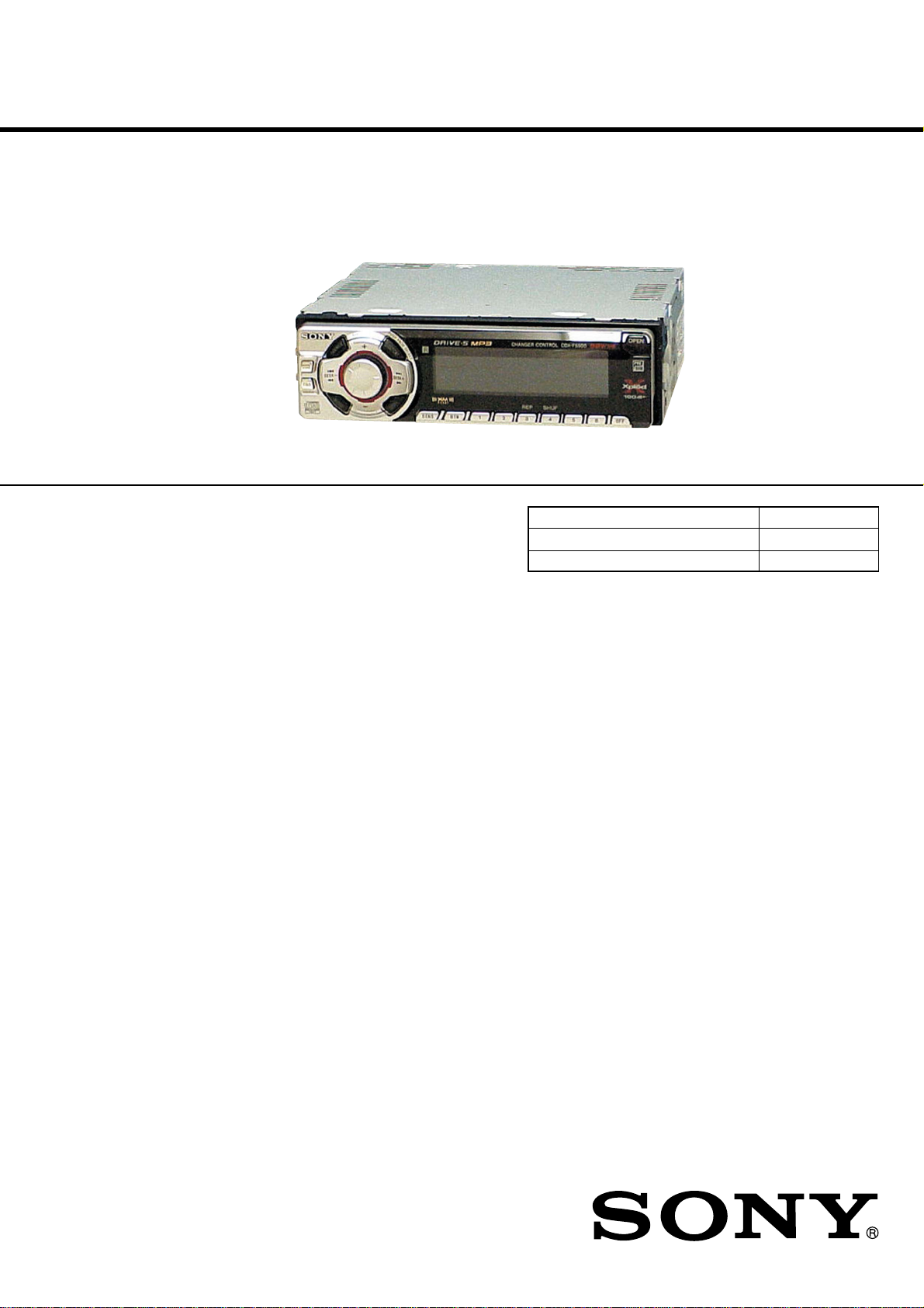
Photo: CDX-F5500
• The tuner and CD sections have no adjustments.
AUDIO POWER SPECIFICATIONS
POWER OUTPUT AND TOTAL HARMONIC DISTORTION
23.2 watts per channel minimum continuous average power into
4 ohms, 4 channels driven from 20 Hz to 20 kHz with no more
than 5% total harmonic distortion.
SPECIFICATIONS
CD player section
Signal-to-noise ratio 120 dB
Frequency response 10 – 20,000 Hz
Wow and flutter Below measurable limit
Tuner section
FM
Tuning range US, Canadian Model:
87.5 – 107.9 MHz
E model:
FM tuning interval:
50 kHz/200 kHz switchable
87.5 – 108 MHz (at 50 kHz step)
87.5 – 107.9 MHz (at 200 kHz step)
Antenna terminal External antenna connector
Intermediate frequency 10.7 MHz/450 kHz
Usable sensitivity 9 dBf
Selectivity 75 dB at 400 kHz
Signal-to-noise ratio 67 dB (stereo),
69 dB (mono)
Harmonic distortion at 1 kHz
0.5% (stereo),
0.3% (mono)
Separation 35 dB at 1 kHz
Frequency response 30 – 15,000 Hz
US Model
Canadian Model
CDX-F5500
E Model
CDX-F5500X
Model Name Using Similar Mechanism CDX-3300/3300S
CD Drive Mechanism Type MG-611MA-186//K
Optical Pick-up Name KSS1000E
AM
Tuning range US, Canadian Model:
530 – 1,710 kHz
E Model:
AM tuning interval:
9 kHz/10 kHz switchable
531 – 1,602 kHz (at 9 kHz step)
530 – 1,710 kHz (at 10 kHz step)
Antenna terminal External antenna connector
Intermediate frequency 10.7 MHz/450 kHz
Sensitivity 30 µV
Power amplifier section
Outputs Speaker outputs
(sure seal connectors)
Speaker impedance 4 – 8 ohms
Maximum power output 52 W × 4 (at 4 ohms)
General
Outputs Audio outputs terminal (front, rear/sub switchable)
Power antenna relay control terminal
Power amplifier control terminal
Inputs Telephone ATT control terminal
Remote controller input terminal
BUS control input terminal
BUS audio input terminal
Antenna input terminal
9-961-449-01
2003L04-1
© 2003. 12
FM/AM COMPACT DISC PLAYER
Sony Corporation
e Vehicle Company
Published by Sony Engineering Corporation
1
Page 2
CDX-F5500/F5500X
Tone controls Low: ±10 dB at 60 Hz (XPLOD)
Mid: ±10 dB at 1 kHz (XPLOD)
High: ±10 dB at 10 kHz (XPLOD)
Power requirements 12 V DC car battery
(negative ground)
Dimensions Approx. 178 × 50 × 177 mm
(7 1/8 × 2 × 7 in.) (w/h/d)
Mounting dimensions Approx. 182 × 53 × 161 mm
(7 1/4 × 2 1/8 × 6 3/8 in.) (w/h/d)
Mass Approx. 1.2 kg
(2 lb. 10 oz.)
Supplied accessories Parts for installation and connections (1 set)
Front panel case (1)
Card remote commander RM-X115
Note
This unit cannot be connected to a digital preamplifier or an equalizer which is Sony
BUS system compatible.
Design and specifications are subject to change without
notice.
SERVICE NOTES
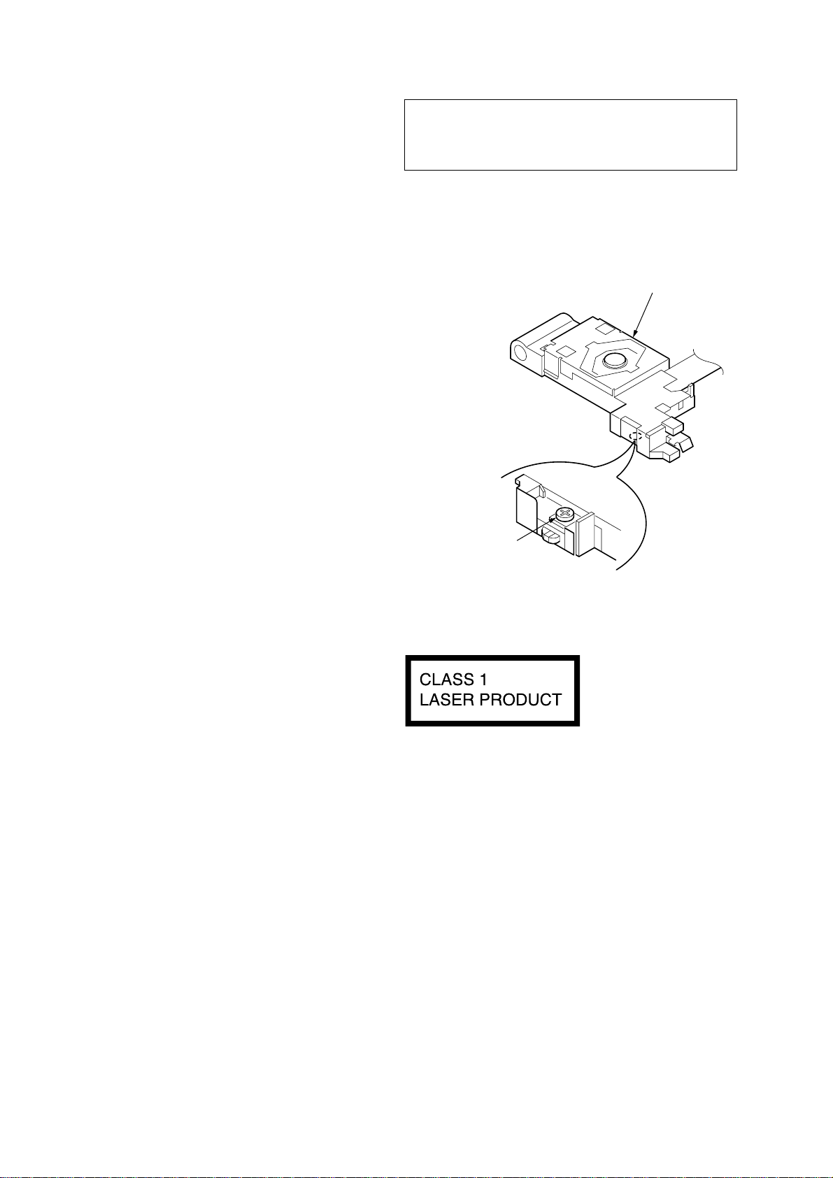
NOTES ON HANDLING THE OPTICAL PICK-UP BLOCK
OR BASE UNIT
The laser diode in the optical pick-up block may suffer electrostatic
breakdown because of the potential difference generated by the
charged electrostatic load, etc. on clothing and the human body.
During repair, pay attention to electrostatic breakdown and also use
the procedure in the printed matter which is included in the repair
parts.
The flexible board is easily damaged and should be handled with
care.
CAUTION
Use of controls or adjustments or performance of procedures
other than those specified herein may result in hazardous
radiation exposure.
If the optical pick-up block is defective, please replace the whole
optical pick-up block.
Never turn the semi-fixed resistor located at the side of optical
pick-up block.
optical pick-up
semi-fixed resistor
NOTES ON LASER DIODE EMISSION CHECK
The laser beam on this model is concentrated so as to be focused on
the disc reflective surface by the objective lens in the optical pickup block. Therefore, when checking the laser diode emission, observe from more than 30 cm away from the objective lens.
Notes on Chip Component Replacement
• Never reuse a disconnected chip component.
• Notice that the minus side of a tantalum capacitor may be dam-
aged by heat.
TEST DISCS
This set can playback CD-R and CD-ROM discs. The following
test discs should be used to check the capability:
CD-R test disc TCD-R082LMT (Part No. J-2502-063-1)
CD-RW test disc TCD-W082L (Part No. J-2502-063-2)
SAFETY-RELATED COMPONENT WARNING!!
COMPONENTS IDENTIFIED BY MARK 0 OR DOTTED LINE
WITH MARK 0 ON THE SCHEMATIC DIAGRAMS AND IN
THE PARTS LIST ARE CRITICAL TO SAFE OPERATION.
REPLACE THESE COMPONENTS WITH SONY PARTS WHOSE
PART NUMBERS APPEAR AS SHOWN IN THIS MANUAL OR
IN SUPPLEMENTS PUBLISHED BY SONY.
• E model
This label is located on the bottom of the chassis.
ATTENTION AU COMPOSANT AYANT RAPPORT
À LA SÉCURITÉ!!
LES COMPOSANTS IDENTIFIÉS P AR UNE MARQUE 0 SUR LES
DIAGRAMMES SCHÉMATIQUES ET LA LISTE DES PIÈCES
SONT CRITIQUES POUR LA SÉCURITÉ DE FONCTIONNEMENT .
NE REMPLACER CES COMPOSANTS QUE PAR DES PIÈCES
SONY DONT LES NUMÉROS SONT DONNÉS DANS CE MANUEL
OU DANS LES SUPPLÉMENTS PUBLIÉS PAR SONY.
2
Page 3
CDX-F5500/F5500X
D
Notes on CD-Rs (recordable CDs)/CD-RWs (rewritable
CDs)
This unit can play the following discs:
Type of discs Label on the disc
Audio CD
MP3 files
• Some CD-Rs/CD-RWs (depending on the equipment used for
its recording or the condition of the disc) may not play on this
unit.
• You cannot play a CD-R/CD-RW that is not finalized∗.
• You can play MP3 files recorded on CD-ROMs, CD-Rs, and
CD-RWs.
• A CD-R/CD-RW to which a session can be added can be played.
z
UNLEADED SOLDER
Boards requiring use of unleaded solder are printed with the lead
free mark (LF) indicating the solder contains no lead.
(Caution: Some printed circuit boards may not come printed with
the lead free mark due to their particular size.)
: LEAD FREE MARK
Unleaded solder has the following characteristics.
• Unleaded solder melts at a temperature about 40°C higher than
ordinary solder.
Ordinary soldering irons can be used but the iron tip has to be
applied to the solder joint for a slightly longer time.
Soldering irons using a temperature regulator should be set to
about 350°C.
Caution: The printed pattern (copper foil) may peel away if the
heated tip is applied for too long, so be careful!
• Strong viscosity
Unleaded solder is more viscous (sticky, less prone to flow)
than ordinary solder so use caution not to let solder bridges
occur such as on IC pins, etc.
• Usable with ordinary solder
It is best to use only unleaded solder but unleaded solder may
also be added to ordinary solder.
∗ A process necessary for a recorded CD-R/CD-RW disc to be
played on the audio CD player.
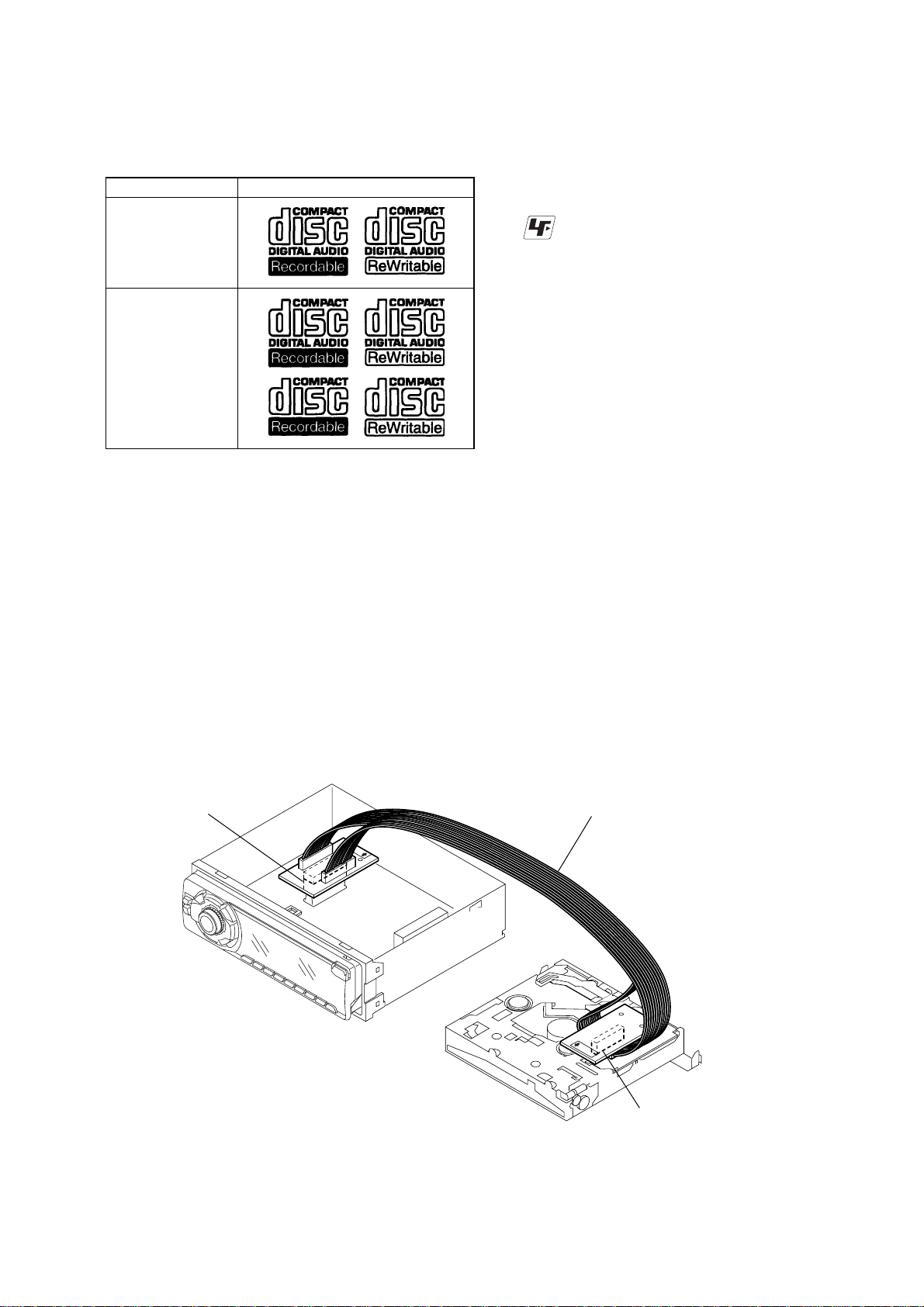
EXTENSION CABLE AND SERVICE POSITION
When repairing or servicing this set, connect the jig (extension cable)
as shown below.
• Connect the MAIN board (CN751) and the SERVO board (CN2)
with the extension cable (Part No. J-2502-076-1).
MAIN BOARD
CN751
J-2502-076-1
SERVO BOAR
CN2
3
Page 4

CDX-F5500/F5500X
TABLE OF CONTENTS
1. GENERAL
Location of Controls (US, Canadian Model) .......................... 5
Location of Controls (E Model) .............................................. 5
Connections (US, Canadian Model)........................................ 6
Connections (E Model) ........................................................... 7
2. DISASSEMBLY
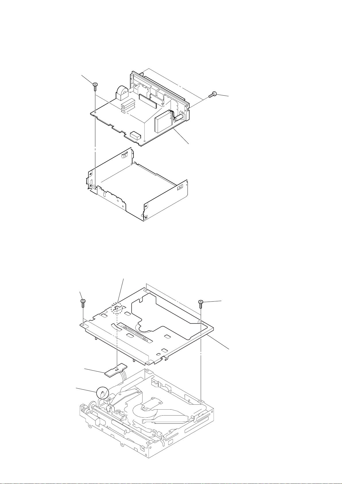
2-1. Sub Panel Assy (CD)........................................................... 9
2-2. CD Mechanism Block ......................................................... 9
2-3. Main Board ....................................................................... 10
2-4. Chassis (T) Sub Assy ........................................................ 10
2-5. Roller Arm Assy ................................................................ 11
2-6. Chassis (OP) Assy............................................................. 11
2-7. Optical Pick-up ................................................................. 12
2-8. SL Motor Assy (M902) .....................................................12
2-9. LE Motor Assy (M903)..................................................... 13
2-10. Servo Board....................................................................... 13
3. DIAGRAMS
3-1. IC Pin Descriptions ........................................................... 14
3-2. Block Diagram –CD Section–........................................... 19
3-3. Block Diagram –Main Section–........................................ 20
3-4. Block Diagram –Display Section–.................................... 21
3-5. Circuit Boards Location .................................................... 21
3-6. Note for Printed Wiring Boards and
Schematic Diagrams ..........................................................22
3-7. Waveforms......................................................................... 22
3-8. Printed Wiring Boards –CD Mechanism Section–............ 23
3-9. Schematic Diagram –CD Mechanism Section (1/2)– ....... 24
3-10. Schematic Diagram –CD Mechanism Section (2/2)– ....... 25
3-11. Schematic Diagram –Main Section (1/2)– ........................26
3-12. Schematic Diagram –Main Section (2/2)– ........................27
3-13. Printed Wiring Boards –Main Section– ............................ 28
3-14. Printed Wiring Board –Relay Section– ............................. 29
3-15. Schematic Diagram –Relay Section–................................ 29
3-16. Printed Wiring Board –Display Section– .......................... 30
3-17. Schematic Diagram –Display Section–............................. 31
3-18. IC Block Diagrams............................................................ 32
4. EXPLODED VIEWS
4-1. Main Section ..................................................................... 33
4-2. Front Panel Section ........................................................... 34
4-3. CD Mechanism Section (1) ...............................................35
4-4. CD Mechanism Section (2) ...............................................36
4-5. CD Mechanism Section (3) ...............................................37
4-6. CD Mechanism Section (4) ...............................................38
5. ELECTRICAL PARTS LIST......................................... 39
4
Page 5
SECTION 1
GENERAL
CDX-F5500/F5500X
This section is extracted
from instruction manual.
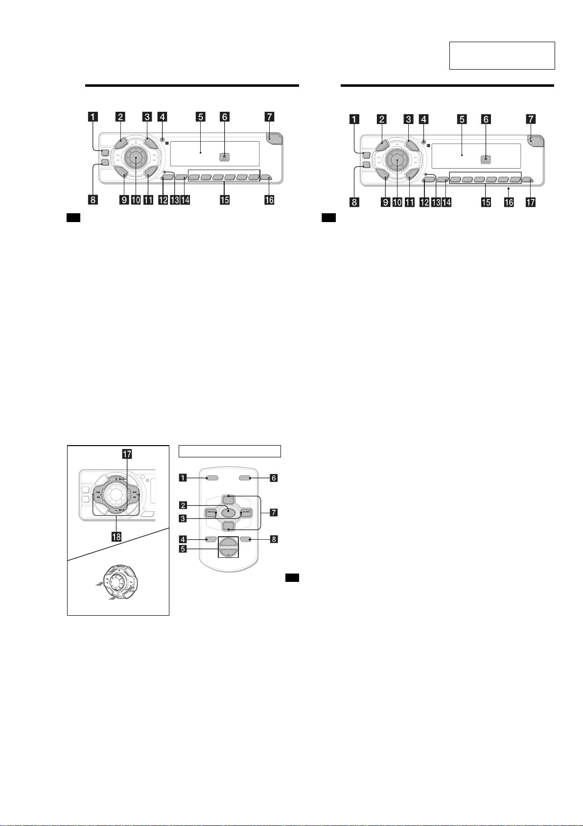
Location of controls
(US, Canadian Model) (E Model)
Refer to the pages listed for details.
P
U
R
E
P
/
S
C
S
E
S
T
I
H
D
D
I
A
L
22
10, 11
L
I
S
S
T
C
A
T
L
P
S
D
14, 15, 18
E
L
E
C
T
BTMSENS
11
E
C
R
U
O
S
DSO
SEEK SEEK
EQ3
M
O
D
E
a DSO button
b SOURCE (Power on/Radio/CD/MD)
button
To s el ect the source.
c LIST/CAT*
d Receptor for the card remote
e Display window
f Z (eject) button (located on the front side
g OPEN button
h EQ3 button
i MODE button
j Volume control dial/Select button
k DSPL (display mode change) button
1
button
commander
of the unit, behind the front panel)
21, 22
To c hange operation.
Rotate to:
– Adjust the volume.
– Adjust settings.
Press to:
– Select items.
12, 14, 21
11,
BBESHUFREP
21
CDX-F5500
l SENS button
m RESET button (located on the front side of
the unit, behind the front panel)
n BTM button
o Number buttons
Radio:
To s t ore stations/receive stored stat ion s.
CD/MD:
(3): REP
(4): SHUF
p OFF (Stop/Power off) button*
*1 (CAT)
is available only when the XM tuner is
connected.
*2
Warning when installing in a car without
an ACC (accessory) position on the
ignition switch
er turning off the ignition, be sure to press
Aft
(OFF)
and hold
disappears.
Otherwise, the display does not turn off and this
causes battery drain.
6543
OFF
16
21
13
13
on the unit until the display
OPEN
Location of controls
Refer to the pages listed for details.
P
U
R
E
P
/
S
C
S
E
S
T
I
H
D
D
I
A
E
C
R
U
O
S
DSO
SEEK SEEK
EQ3
M
O
D
E
a DSO button 23
b SOURCE (Power on/Radio/CD/MD)
9
2
10, 11
button
To s el ect the source.
c LIST
button 14, 15, 18
d Receptor for the card remote
commander
e Display window
f Z (eject) button (located on the front side
of the unit, behind the front panel) 11
g OPEN button 10, 11
h EQ3 button 22
i MODE button
To c hange operation.
j Volume control dial/Select button
Rotate to:
– Adjust the volume.
– Adjust settings.
Press to:
– Select items.
k DSPL (display mode change) button
11, 12, 14, 21
l SENS button 16
L
L
S
I
E
S
L
T
E
C
T
L
P
S
D
21
BTMSENS
CDX-F5500X
m RESET button (located on the front side of
the unit, behind the front panel) 9
n BTM button
o Number buttons 21
Radio:
To s t ore stations/receive stored stati on s.
CD/MD:
(3): REP 13
(4): SHUF 13
p Frequency select swi
bottom of the unit)
See “Frequency select switch” in the
Installation/Connections manual.
q OFF (Stop/Power off) button* 10, 11
* Warning when installing in a car without
an ACC (accessory) position on the
ignition switch
After turning off the ignition, be sure to press
and hold (OFF) on the unit until the display
disappears.
Otherwise, the display does not turn off and this
causes battery drain.
BBESHUFREP
6543
OFF
(located on the
tch
OPEN
4
P
U
R
E
P
/
S
C
S
E
S
T
I
H
D
D
I
A
L
E
C
R
U
O
S
DSO
SEEK SEEK
EQ3
M
O
D
E
(DISC/PRESET)
(+): to select upwards
(SEEK)
(–): to select
q DISC (ALBUM)/PRESET buttons (+/–)
To r e ceive preset stations/change the disc*
skip albums*
*1
*2
r SEEK buttons (–/+)
To s k ip tracks/fast-forward, reverse a track/
tune in stations automatically, find a station
manually/select a setting.
S
leftwards/
.
(DISC/PRESET)
(–): to select downwards
2
.
When an optional CD/MD unit is connected.
Available only when an MP3 file is played.
L
I
S
S
E
T
L
C
E
A
C
T
T
L
P
S
D
SENS
(SEEK)
SEEK
(+): to select
rightwards/
>
E
E
K
Card remote commander RM-X115
DSPL MODE
+
PRESET
SOURCE
–
SEEK
PRESET
–
+
VOL
–
The corresponding buttons of the card
remote commander control the same
functions as those on this unit.
a DSPL button
b SOURCE button
c SEEK (–/+) buttons
d OFF button
1
,
e VOL (+/–) buttons
f MODE button
g PRESE
T (DISC/ALBUM) (+/–) buttons
h AT T bu tt o n
Note
If the display disappears by pressing
be operated with the card remote commander unless
(SOURCE)
on the unit is pressed, or a di sc i s in se rted
to activate the unit first.
Tip
For details on how to replace the battery, see
“Replacing the lithium battery” on page 23.
continue to next page t
4
+
SEEK
AT TOFF
(OFF)
, it cannot
5
5
Page 6
CDX-F5500/F5500X
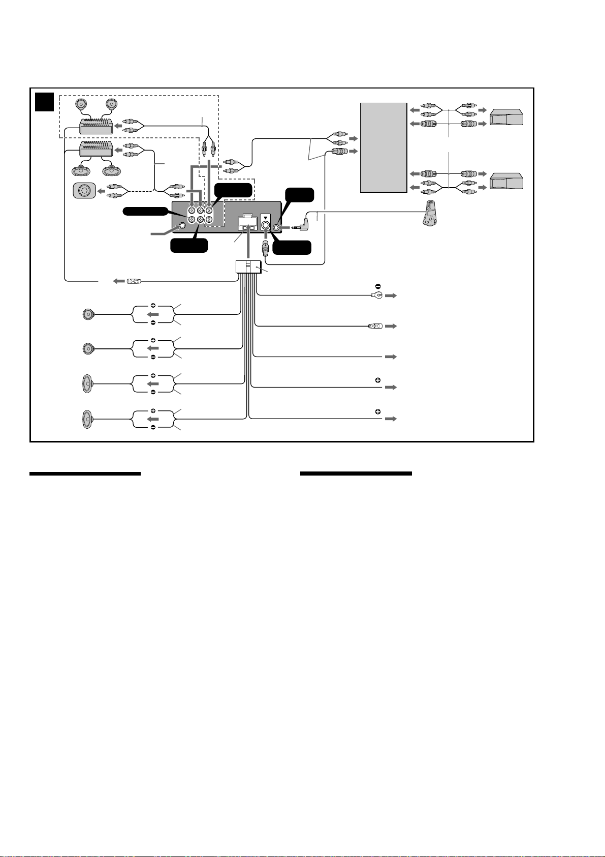
Connections (US, Canadian Model)
3
from car antenna
à partir de l’antenne de la voiture
3
Left
Gauche
Right
Droit
Left
Gauche
Right
Droit
CDX-F5500 only
CDX-F5500 uniquement
1
*
BUS AUDIO IN
AMP REM
Max. supply current 0.3 A
Courant max. fourni 0,3 A
L
R
AUDIO OUT
REAR
Blue/white striped
Rayé bleu/blanc
White
Blanc
White/black striped
Rayé blanc/noir
Gray
Gris
Gray/black striped
Rayé gris/noir
Green
Vert
Green/black striped
Rayé vert/noir
Purple
Mauve
Purple/black striped
Rayé mauve/noir
*
1
*
2
AUDIO OUT
FRONT
Fuse (10 A)
Fusible (10 A)
Supplied with XA-C30
Fourni avec le XA-C30
REMOTE
BUS
CONTROL IN
4
Black
Noir
Blue
Bleu
Light blue
Bleu ciel
Red
Rouge
Yellow
Jaune
IN
3
*
Max. supply current 0.1 A
Courant max. fourni 0,1 A
ANT REM
Source selector
(not supplied)
Sélecteur de source
(non fourni)
XA-C30
ATT
Supplied with the CD/MD changer
Fourni avec le changeur de CD/MD
1
*
RCA pin cord (not supplied)
2
*
AUDIO OUT can be switched to REAR
or SUB.
For details, see the supplied operating
instructions.
3
*
Insert with the cord upwards.
1
*
Cordon à broche RCA (non fourni)
2
*
AUDIO OUT peut être commuté sur
1
REAR ou SUB.
Pour obtenir plus de détails, reportezvous au mode d'emploi fourni.
3
*
Insérez avec le câble vers le bas.
2
4
5
6
Connection diagram (3)
1
To a metal surface of the car
First connect the black ground lead, then
connect the yellow and red power input leads.
2
To the power antenna control lead or power
supply lead of antenna booster amplifier
Notes
• It is not necessary to connect this lead if there
is no power antenna or antenna booster, or
with a manually-operated telescopic antenna.
• When your car has a built-in FM/AM antenna in
the rear/side glass, see “Notes on the control
and power supply leads.”
3
To AMP REMOTE IN of an optional power
amplifier
This connection is only for amplifiers. Connecting
any other system may damage the unit.
4
To the interface cable of a car telephone
5
To the +12 V power terminal which is energized
in the accessory position of the ignition key
switch
Notes
• If there is no accessory position, connect to the
+12 V power (battery) terminal which is
energized at all times.
Be sure to connect the black ground lead to a
metal surface of the car first.
• When your car has a built-in FM/AM antenna in
the rear/side glass, see “Notes on the control
and power supply leads.”
6
To the +12 V power terminal which is energized
at all times
Be sure to connect the black ground lead to a
metal surface of the car first.
Notes on the control and power supply leads
• The power antenna control lead (blue) supplies
+12 V DC when you turn on the tuner.
• When your car has built-in FM/AM antenna in the
rear/side glass, connect the power antenna control
lead (blue) or the accessory power input lead (red)
to the power terminal of the existing antenna
booster. For details, consult your dealer.
•A power antenna without a relay box cannot be
used with this unit.
Memory hold connection
When the yellow power input lead is connected,
power will always be supplied to the memory circuit
even when the ignition switch is turned off.
Notes on speaker connection
• Before connecting the speakers, turn the unit off.
• Use speakers with an impedance of 4 to 8 ohms,
and with adequate power handling capacities to
avoid its damage.
• Do not connect the speaker terminals to the car
chassis, or connect the terminals of the right
speakers with those of the left speaker.
• Do not connect the ground lead of this unit to the
negative (–) terminal of the speaker.
• Do not attempt to connect the speakers in parallel.
• Connect only passive speakers. Connecting active
speakers (with built-in amplifiers) to the speaker
terminals may damage the unit.
•To avoid a malfunction, do not use the built-in
speaker leads installed in your car if the unit shares
a common negative (–) lead for the right and left
speakers.
• Do not connect the unit’s speaker leads to each
other.
Note on connection
If speaker and amplifier are not connected correctly,
“FAILURE” appears in the display. In this case, make
sure the speaker and amplifier are connected
correctly.
Schéma de raccordement (3)
1
À un point métallique de la voiture
Branchez d‘abord le fil de masse noir et, ensuite,
les fils d‘entrée d‘alimentation jaune et rouge.
2
Vers le fil de commande de l‘antenne électrique
ou le fil d‘alimentation de l‘amplificateur
d‘antenne
Remarques
•Il n'est pas nécessaire de raccorder ce fil s'il n'y a
pas d'antenne électrique ni d'amplificateur
d'antenne, ou avec une antenne télescopique
manuelle.
•Si v otre voiture est équipée d'une antenne FM/
AM intégrée dans la vitre arrière/latérale, voir
« Remarques sur les fils de commande et
d'alimentation ».
3
Au niveau du AMP REMOTE IN de l’amplificateur
de puissance en option
Ce raccordement s’applique uniquement aux
amplificateurs. Le branchement de tout autre
système risque d’endommager l’appareil.
4
Vers le cordon de liaison d’un téléphone de
voiture
5
À la borne +12 V qui est alimentée quand la clé
de contact est sur la position accessoires
Remarques
•S'il n'y a pas de position accessoires, raccordez la
borne d'alimentation (batterie) +12 V qui est
alimentée en permanence.
Raccordez d’abord le fil de masse noir à un
point métallique du véhicule.
•Si v otre voiture est équipée d'une antenne FM/
AM intégrée dans la vitre arrière/latérale, voir
« Remarques sur les fils de commande et
d'alimentation ».
6
À la borne +12 V qui est alimentée en
permanence
Raccordez d’abord le fil de masse noir à un point
métallique du véhicule.
Remarques sur les fils de commande et
d
’
alimentation
• Le fil de commande de l’antenne électrique (bleu)
fournit une alimentation de +12 V CC lorsque vous
mettez la radio sous tension.
• Lorsque votre voiture est équipée d’une antenne
FM/AM intégrée dans la vitre arrière/latérale,
raccordez le fil de commande de l’antenne (bleu)
ou l’entrée d’alimentation des accessoires (rouge) à
la borne d’alimentation de l’amplificateur
d’antenne existant. Pour plus de détails, consultez
votre détaillant.
• Une antenne électrique sans boîtier de relais ne
peut pas être utilisée avec cet appareil.
Raccordement pour la conservation de la mémoire
Lorsque le fil d’entrée d’alimentation jaune est
raccordé, le circuit de la mémoire est alimenté en
permanence même si la clé de contact est sur la
position d’arrêt.
Remarques sur le raccordement des haut-parleurs
•Avant de raccorder les haut-parleurs, mettez
l’appareil hors tension.
• Utilisez des haut-parleurs ayant une impédance de
4 à 8 ohms avec une capacité électrique adéquate
pour éviter de les endommager.
• Ne raccordez pas les bornes du système de hautparleurs au châssis de la voiture et ne raccordez pas
les bornes des haut-parleurs droit à celles du hautparleur gauche.
• Ne raccordez pas le câble de masse de cet appareil à
la borne négative (–) de l’enceinte.
•N’essa yez pas de raccorder les haut-parleurs en
parallèle.
• Raccordez uniquement des haut-parleurs passifs. Le
raccordement de haut-parleurs actifs (avec
amplificateurs intégrés) aux bornes des hautparleurs peut endommager l’appareil.
•Pour éviter tout dysfonctionnement, n’utilisez pas
les fils des haut-parleurs intégrés installés dans
votre voiture si l’appareil partage un fil négatif
commun (–) pour les haut-parleurs droit et gauche.
• Ne raccordez pas entre eux les cordons des hautparleurs de l’appareil.
Remarque sur le raccordement
Si les haut-parleurs et l’amplificateur ne sont pas
raccordés correctement, le message « FAILURE »
s’affiche. Dans ce cas, assurez-vous que les hautparleurs et l’amplificateur sont bien raccordés.
6
Page 7
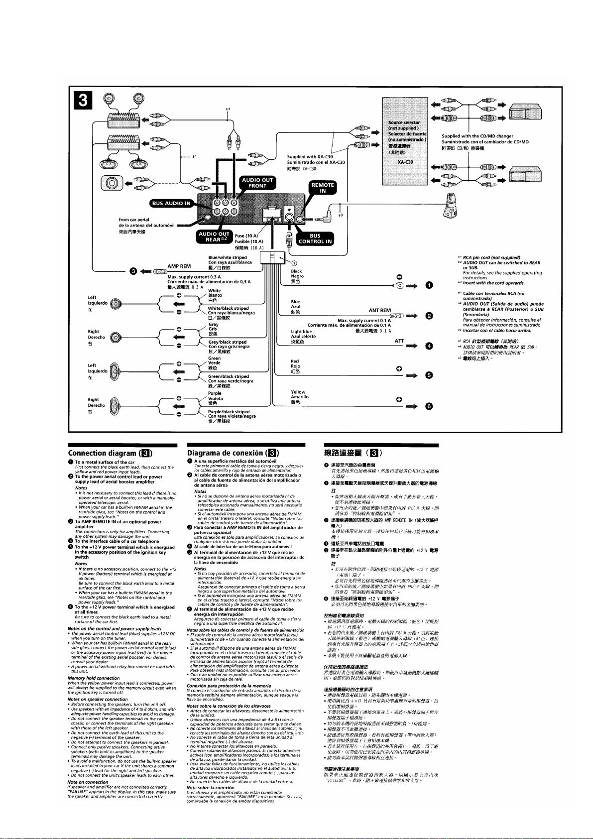
Connections (E Model)
CDX-F5500/F5500X
7
Page 8
CDX-F5500/F5500X
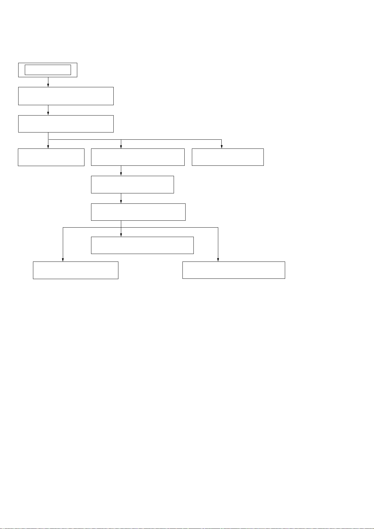
SECTION 2
DISASSEMBLY
Note : This set can be disassemble according to the following sequence.
SET
2-1. SUB PANEL ASSY (CD)
(Page 9)
2-2. CD MECHANISM BLOCK
(Page 9)
2-3. MAIN BOARD
(Page 10)
2-7. OPTICAL PICK-UP
(Page 12)
2-4. CHASSIS (T) SUB ASSY
(Page 10)
2-5. ROLLER ARM ASSY
(Page 11)
2-6. CHASSIS (OP) ASSY
(Page 11)
2-8. SL MOTOR ASSY (M902)
(Page 12)
2-10. SERVO BOARD
(Page 13)
2-9. LE MOTOR ASSY (M903)
(Page 13)
8
Page 9
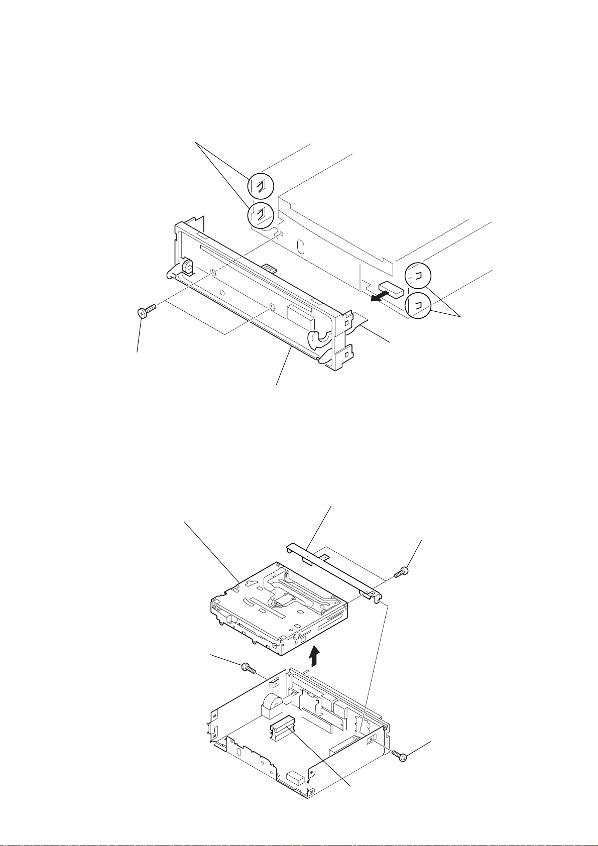
Note : Follow the disassembly procedure in the numerical order given.
s
)
2-1. SUB PANEL ASSY (CD)
3
two claws
4
CDX-F5500/F5500X
2
two claw
1
two
screws
(+PTT 2.6
x
6)
2-2. CD MECHANISM BLOCK
5
CD mechanism block
5
sub panel assy (CD)
7
bracket (CD)
CNP802
6
two
screws
(+PTT 2.6
x
6)
2
screw
(+PTT 2.6
x
6)
3
4
CN751
1
screw
(+PTT 2.6
x
6
9
Page 10
CDX-F5500/F5500X
)
2-3. MAIN BOARD
1
three screws
(+BTT)
3
MAIN board
2
two
screws
(+PTT 2.6
x
8
2-4. CHASSIS (T) SUB ASSY
2
two
screws
(+P 1.7
5
SENSOR board
3
claw
x
2.2)
4
claw
1
two
screws
x
(+P 1.7
6
2.2)
chassis (T) sub assy
10
Page 11
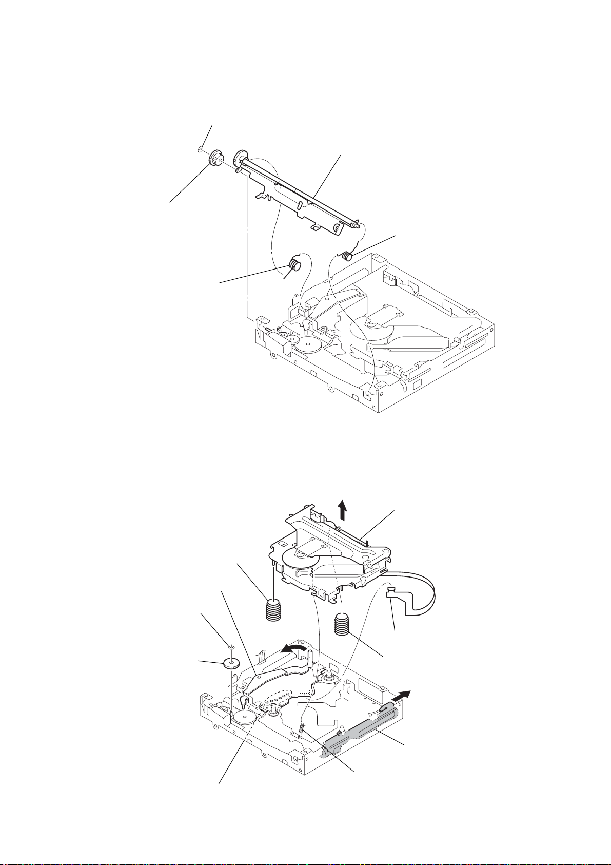
2-5. ROLLER ARM ASSY
)
4
worm wheel (RA)
1
spring (RAL)
3
washer (1.1 – 2.5)
5
roller arm assy
2
spring (RAR)
CDX-F5500/F5500X
2-6. CHASSIS (OP) ASSY
0
compression spring (damper)
4
washer
5
gear (LE1)
lever (D)
6
8
qa
chassis (OP) assy
1
CN1
9
two compression springs (damper
7
slider (R)
2
Remove the six solderings.
3
tension coil spring (KF)
11
Page 12
CDX-F5500/F5500X
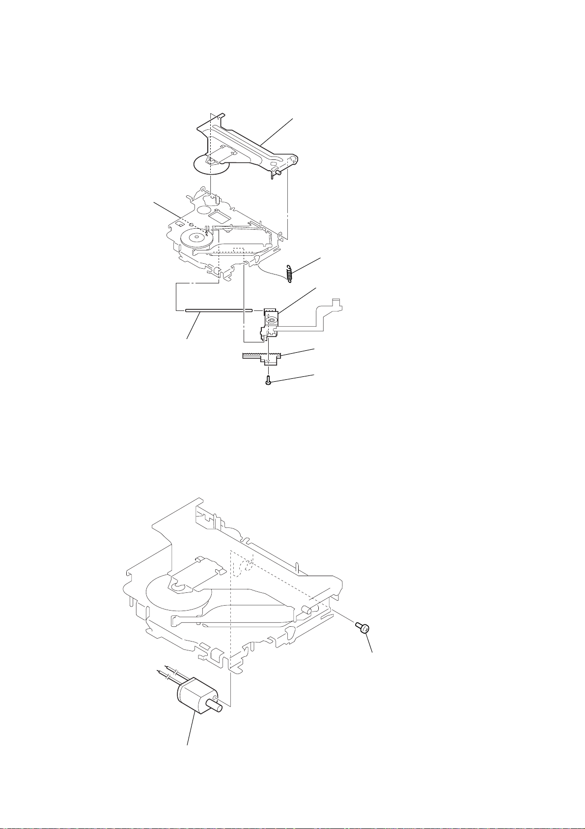
2-7. OPTICAL PICK-UP
5
claw
2
chucking arm sub assy
1
tension coil spring (CHKG)
7
optical pick-up
2-8. SL MOTOR ASSY (M902)
6
main shaft
4
rack (SL)
3
screw
(+B 1.4
x
5)
12
2
SL motor assy (M902)
1
screw
(+P 1.4
x
1.8)
Page 13
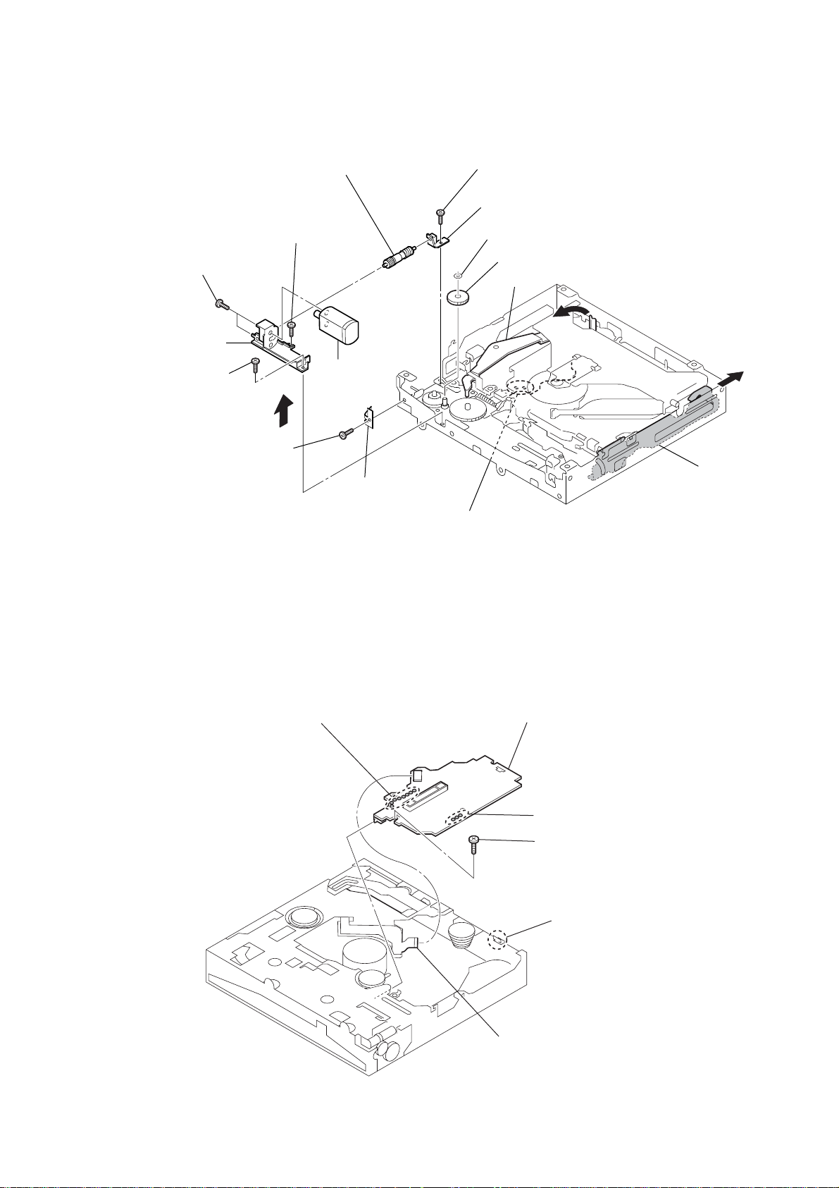
2-9. LE MOTOR ASSY (M903)
qf
two toothed lock
(+M 1.4
bracket (LEM)
qs
screw
(+M 1.7
x
)
screws
2.5)
6
screw
(+P 1.7
x
qd
2.2)
qa
screw
(+M 1.7
qg
(M903)
0
woam (LEB) assy
x
2.5)
LE motor assy
7
leaf spring (LE)
8
screw
(+M 1.7
9
bearing (LEB)
2
washer
gear (LE1)
3
lever (D)
x
CDX-F5500/F5500X
2.5)
4
5
slider (R)
2-10. SERVO BOARD
1
Remove the eight solderings.
1
Remove the soldering.
6
SERVO board
2
Remove the three solderings.
4
toothed lock
(M 1.7)
5
screw
claw
3
CN1
13
Page 14

CDX-F5500/F5500X
SECTION 3
DIAGRAMS
3-1. IC PIN DESCRIPTIONS
• IC3 CXD3059AR (DIGITAL SERVO/DIGITAL SIGNAL PROCESSOR) (SERVO BOARD (1/2))
Pin No. Pin Name I/O Pin Description
1 MIRR I/O Mirrer signal input/output
2 DFCT I/O Defect signal input/output
3 FOK I/O Focus OK signal input/output
4 VSS — Ground pin
5 LOCK I/O Not used in this set. (Open)
6 MDP O Spindle motor servo control signal output
7 SSTP I Disc most inner detection signal input
8IOVSS1 — Digital ground pin for I/O
9 SFDR O Sled drive signal output
10 SRDR O Sled drive signal output
11 TFDR O Tracking drive signal output
12 TRDR O Tracking drive signal output
13 FFDR O Focus drive signal output
14 FRDR O Focus drive signal output
15 IOVDD1 — Digital power supply pin for I/O
16 AVDD0 — Analog power supply pin for I/O
17 AVSS0 — Analog ground pin
18 NC — Not used. (Open)
19 E I E signal input
20 F I F signal input
21 TEI I Tracking error signal input from the DSSP block
22 TEO O Tracking error signal output to the RF amp block
23 FEI I Focus error signal input from the DSSP block
24 FEO O Focus error signal output form the RF amp block
25 VC I/O
26 A I A signal input
27 B I B signal input
28 C I C signal input
29 D I D signal input
30 NC — Not used. (Open)
31 AVDD4 — Analog power supply pin
32 RFDCO I/O
33 PDSENS I Reference voltage input for PD
34 AC SUM O RFAC suming amp signal output
35 EQ IN I Equalizer circuit signal input
36 LD O APC amp signal output
37 PD I APC amp signal input
38 NC — Not used. (Open)
39 RFC I EQ cut off frequency adjustment input
40 AVSS4 — Analog ground pin
41 RFACO O RFAC signal output
42 RFACI I RFAC signal input or EFM signal input
43 AVDD3 — Analog power supply pin
44 BIAS I Asymmetry circuit constant current input
45 ASYI I Asymmetry comparate voltage input
46 ASYO O EFM full swing signal output
47 VPCO O Charge pomp output for wideband EFM PLL
48 VCTL I VCO2 control voltage input for wideband EFM PLL
49 AVSS3 — Analog ground pin
VC voltage output to the RF amp block
Center voltage input from the DSSP block by command select
RFDC signal output
RFDC signal input from the DSSP block by command select
14
Page 15

CDX-F5500/F5500X
Pin No. Pin Name I/O Pin Description
50 CLTV I VCO1 control voltage input
51 FILO O Filter signal output for master PLL
52 FILI I Filter signal input for master PLL
53 PCO O Charge pomp output for master PLL
54 AVDD5 — Analog power supply pin
55 DDVROUT O DC/DC converter output
56 DDVRSEN I DC/DC converter output voltage monitor signal input
57 AVSS5 — Analog ground pin
58 DDCR I Reset signal input for DC/DC converter
59 NC — Not used. (Open)
60 BCKI I D/A interface bit clock signal input
61 PCMDI I D/A interface serial data signal input
62 LRCKI I D/A interface LR clock signal input
63 LRCK O D/A interface LR clock signal output
64 VSS — Digital ground pin for internal
65 PCMD O D/A interface serial data signal output
66 BCK O D/A interface bit clock signal output
67 VDD — Digital power supply pin for internal
68 EMPH O Not used in this set. (Open)
69 EMPHI I Not used in this set. (Fixed at “L”.)
70 IOVDD2 — Digital power supply pin for I/O
71 DOUT O Digital out signal output
72, 73 TEST I Test pin Normally “L”.
74 IOVSS2 — Digital ground pin for I/O
75 NC — Not used in this set. (Open)
76 XVSS — Ground pin for master clock
77 XTAO O Crystal oscillation circuit output (16.9344 MHz)
78 XTAI I Crystal oscillation circuit input (16.9344 MHz)
79 XVDD — Power supply pin for master clock
80 AVDD1 — Analog power supply pin
81 AOUT1 O L channel analog signal output
82 VREFL O L channel reference voltage output
83 AVSS1 — Analog ground pin
84 AVSS2 — Analog ground pin
85 VREFR O R channel reference voltage output
86 AOUT2 O R channel analog signal output
87 AVDD2 — Analog power supply pin
88 NC — Not used. (Open)
89 IOVDD0 — Digital power supply pin for I/O
90 RMUT O R channel “O” detection flug output
91 LMUT O L channel “O” detection flug output
92 NC — Not used. (Open)
93 XTSL I X’tal select signal input 16.9344 MHz: “L”, 33.8688 MHz: “H”
94 IOVSS0 — Digital ground pin for I/O
95 XTACN I Oscillation circuit control input “H”: Oscillation start, “L”: Oscillation stop
96 SQSO O Sub 80 bit and PCM peak, level data signal output CD text data signal output
97 SQCK I Clock signal input for SQSO read out
98 SBSO O Sub P-W serial data signal output Not used in this set. (Open)
99 EXCK I Clock signal input for SBSO read out Not used in this set. (Open)
100 XRST I System reset signal input “L”: reset
101 SYSM I Mute signal input “H”: mute Not used in this set. (Fixed at “L”.)
102 DATA I Serial data signal input
103 VSS — Digital ground pin for internal
15
Page 16

CDX-F5500/F5500X
Pin No. Pin Name I/O Pin Description
104 XLAT I Latch signal input
105 CLOK I Serial data transfer clock signal input
106 VDD — Digital power supply pin for internal
107 SENS O SENS signal output
108 SCLK I Clock signal input for SENS serial data read out
109 ATSK I/O Input/output for anti-shock
110 WFCK O WFCK signal output Not used in this set. (Open)
111 XUGF O XUGF signal output Not used in this set. (Open)
112 XPCK O XPCK signal output Not used in this set. (Open)
113 GFS O GFS signal output
114 C2PO O C2PO signal output
115 SCOR O Sub cord sync signal output
116 VDD — Digital power supply pin for internal
117 C4M O 4.2336 MHz signal output Not used in this set. (Open)
118 WDCK O Word clock signal output Not used in this set. (Open)
119 COUT I/O Track count signal input/output Not used in this set. (Open)
120 NC — Not used. (Open)
16
Page 17

CDX-F5500/F5500X
• IC801 MB90487PF-G-103-BNDE1 (SYSTEM CONTROL) (MAIN BOARD (2/2))
Pin No. Pin Name I/O Pin Description
1ATT O Audio mute control signal output
2 to 4 NC — Not used in this set. (Open)
5 BEEP O Beep signal output to power amp IC
6VOL ATT O Electrical volume ATT control output
7 to 10 NC — Not used in this set. (Open)
11 VSS — Ground pin
12 to 14 NC — Not used in this set. (Open)
15 TU ATT O Tuner mute control output
16, 17 NC — Not used in this set. (Open)
18 CD SI I CD servo serial data signal input Not used in this set. (Open)
19 CD SO O CD servo serial data signal output Not used in this set. (Open)
20 CD SCK O CD servo serial clock signal output Not used in this set. (Open)
21 RE 0 I Rotary encoder signal input 0
22 RE 1 I Rotary encoder signal input 1
23 VCC+3.3 — Power supply pin (+3.3 V)
24 EEP SIO I/O Serial data signal input/output for EEPROM communication
25 EEP SCK O Serial clock signal output for EEPROM communication
26 SHUT SW I
27 LCD CE O Chip enable signal output to LCD driver IC
28 LCD SO O Serial data signal output to LCD driver IC Flash: UART serial out
29 LCD SCK O Serial clock signal output to LCD driver IC
30 NC — Not used in this set. (Open)
31 STB O Standby signal output to power amp IC
32 AUX — Not used in this set. (Open)
33 IIC SCK O IIC bus serial clock signal output
34 IIC SIO I/O IIC bus serial data signal input/output
35 VCC+3.3 — Power supply pin (+3.3 V) (for A/D converter)
36 AVRH+3.3 — External reference power supply (+3.3 V) (for A/D converter)
37 AVSS — Ground pin (for A/D converter)
38, 39 KEY IN0, 1 I Key signal input
40 NC — Not used in this set. (Open)
41 RC IN0 I Rotary commander key signal input
42 VSS — Ground pin
43, 44 NC — Not used in this set. (Fixed at “L”.)
45 VSM I S meter voltage detect signal input
46 DST SEL I Destination select pin
47 KEY ACK I Key acknowledge detect signal input
48 NC — Not used in this set. (Open)
49, 50 MD0, 1 I Input for operation mode designation (Fixed at “H”.)
51 MD2 I Input for operation mode designation (Fixed at “L”.)
52 NC — Not used in this set. (Open)
53 BU IN I Back up power supply detect signal input
54 OP REQ/INTQ O OP REQ/INTQ select signal output
55 CD SELFSW I CD mechanism self load position detect switch signal input Not used in this set. (Open)
56 DIAG I Condition input from power amp IC
57 TU ATT IN I Tuner ATT signal input
58 UNI SI I Serial data signal input
59 UNI SO O Serial data signal output
60 UNI SCK O Serial clock signal output
61 BUS ON O Bus on signal output
62 SYS RST O System reset signal output
Shutter switch open/close detect signal input Not used in this set. (Open)
“L”: Panel open, “H”: Panel close
17
Page 18

CDX-F5500/F5500X
Pin No. Pin Name I/O Pin Description
63 TEL A TT O TEL A TT signal output
64 ACC IN I Accessory power supply detect signal input
65 SIRCS I Remote control signal (infrared rays) input
66 RAM BU O Not used in this set. (Fixed at “L”.)
67 TEST IN I Test mode detect signal input
68 FLASH W I
69 NOSE SW I Nose detect switch signal input
70, 71 NC — Not used in this set. (Open)
72 DOOR SW I
73 DOOR IND O Door indicator control signal output
74 RC IN1 I Rotary commander shift key signal input
75 XKEY ON O Key power supply control signal output Pin rj (KEY ACK) active: “L” output
76 NC — Not used in this set. (Open)
77 RESET I Reset signal input
78 NC — Not used in this set. (Open)
79 X1A — Oscillator connect pin (32 kHz)
80 X0A — Oscillator connect pin (32 kHz)
81 VSS — Ground pin
82 X0 — Oscillator connect pin (3.68 MHz)
83 X1 — Oscillator connect pin (3.68 MHz)
84 VCC+3.3 — Power supply pin (+3.3 V)
85 to 88 NC — Not used in this set. (Open)
89 ZERO DET R I Mechanism deck mute zero closs detect signal input R
90 ZERO DET L I Mechanism deck mute zero closs detect signal input L
91 CD STB O
92 CD IN SW I CD mechanism IN-SW detect signal input Not used in this set. (Open)
93 CD LOAD O CD mechanism loading motor control signal output Not used in this set. (Open)
94 CD ON/EJECT O CD mechanism eject motor control signal output
95 CDM ON/D SW I CD mechanism DSW detect signal input
96 CD LIMIT I CD mechanism IN-LIMIT SW signal input Not used in this set. (Open)
97 RFOK I CD servo RFOK signal input
98 CD XRST O CD servo reset signal output Not used in this set. (Open)
99 CD A0 O
100 NC — Not used in this set. (Open)
Memory mode changeover signal input
Normally “H” input (single chip mode) “L” after reset: Flash write mode
Front panel open/close detect signal input
“L” input: Panel close, “H” input: Panel open
CD servo data strob signal output Timing of data latch: “L” output
Not used in this set. (Open)
CD servo command/parameter identification signal output Not used in this set. (Open)
Command transmission: “L” output, parameter transmission: “H” output
18
Page 19

3-2. BLOCK DIAGRAM — CD SECTION —
DETECTOR
PD1
PD2
E
F
LASER DIODE
PICK-UP BLOCK
(KSS1000E)
2-AXIS DEVICE
(FOCUS)
(TRACKING)
PD LD
OPTICAL
PD2
PD1
I-V AMP
PD
FCS+
FCS–
TRK+
TRK–
LD
E
F
AUTOMATIC
CONTROL
M902
(SLED)
M901
(SPINDLE)
M903
(LOADING)
POWER
Q1
RFACO
A
26
B
27
C
28
D
29
19
E
20
F
36
LD
FOCUS/TRACKING COIL DRIVE,
SLED/SPINDLE/LOADING
MOTOR DRIVE
11
VO2–
10
VO2+
13
VO1–
12
VO1+
6
M
M
M
VO4+
7
VO4–
8
VO3+
9
VO3–
5
VOL+
4
VOL–
FEO
TEO
IC1
CDX-F5500/F5500X
• R-ch is omitted due to same as L-ch.
• Siganal Path
: CD PLAY
ASYO
41
24
22
37
PD
VIN2+
VIN2–
VIN1+B
VIN1–B
VIN4+
VIN4–
VIN3+
MUTE
FWD
REV
RFACI
42
FEI
23
TEI
21
22
21
19
18
31
32
25
34
1
2
46
RF AMP,DIGITAL SERVO,
DIGITAL SIGNAL PROCESSOR
IC3
ASYI
45
FFDR
13
FRDR
14
TFDR
11
TRDR
12
SFDR
9
SRDR
10
MDP
6
AOUT1
AOUT2
LMUTE
RMUTE
FOK
SQSO
SQCK
XRST
DATA
XLAT
CLOK
SENS
SCLK
GFS
C2POT
SCOR
XTAI
XTAO
BCK
BCKI
PCMDI
LRCK
LRCKI
PCMD
89
90
96
97
100
102
104
105
107
108
113
114
115
78
77
66
60
61
63
62
65
81
86
R-CH
CD LMUT
22
CD RMUT
23
CD FOK
3
X1
16.934MHz
(DOWN)
(SELF)
(DISC IN)
(LIMIT)
SW1
SW2
SW3
SW4
X2
18.43MHz
19
CD SQSO
16
CD SQCK
18
CD XRST
15
CD DATA
14
CD XLAT
13
CD CLOK
12
CD SENS
11
CD SCLK
10
CD GFS
8
CD C2PO
7
CD SCORT
52
X1
81
X0
80
MEC_DSW
46
MEC_SELFSW
53
MEC_INSW
45
MEC_LIMIT
42
DRON
41
MEC LOAD
43
MEC EJECT
44
SYSTEM CONTROL
CD
IC4
LINK OFF
UNISI
RXD
UNISO
TXD
UNICLK
BUS ON
BU IN
RSTX
A ATT
EJECT OK
OPEN REQ
MECON
CDON
ZMUT
MECON CHK
CDON CHK
DECON
DEC XMUTE
DEC SSTBY
DEC XRST
DEC STBY
DEC INT
DEC SCL
DEC SDA
EMPH
20
56
25
57
26
58
50
51
75
60
SYSTEM CONTROL
61
62
63
64
66
67
68
+1.5V
65
37
27
28
29
30
31
32
69
MECHA+6V
SERVO+3.3V
+1.5V
CONTROL
Q2,3
+3.3V
RF OK
97
OPEN REQ
54
CDM ON
95
CD ON
94
ZERO DET
89
+1.5V REG
IC7
VOUT
+3.3V
CONTROL
Q5,6
CLCK
22
SRMSTB
41
RESET
2
STANDBY
3
BUCK
36
I2C SCL
7
I2C SDA
6
BUSO
28
CD-L
LINK OFF
UNI SI
UNI SO
UNI SCK
BUS ON
BU IN
SYS RST
ATT
IC801 (1/3)
VDD
15
CE
3
AUDIO INTERFACE
IC8
MAIN
A
SECTION
(Page 20)
MAIN
B
SECTION
(Page 20)
U COM+3.3V
19 19
15
18
11
16
19
14
BCK1A
BCK1B
SD0O
LRCK1A
LRCK1B
SD1O
Page 20

CDX-F5500/F5500X
3-3. BLOCK DIAGRAM — MAIN SECTION —
ELECTRONIC VOLUME
PJ601
(ANTENNA)
CD
SECTION
(Page 19)
(TUNER UNIT)
1
ANT
A
TUX601
TU VDD
E2P VDD
TU-SDA
S-METER
TU MUTE
E2P SCL
E2P SDA
VCC
TU-SCL
CD-L
L
R
10
11
15
13
14
16
17
4
3
6
7
R-CH
AU+8V
TU+5V
U COM+3.3V
SCL
SDA
9
8
7
6
45
15
25
24
IC401
C2
C1
B2
B1
VSM
TU ATT
EEP SCK
EEP SIO
OUTS1
OUTS2
OUTF2
OUTR2
OUTF1
OUTR1
MUTE
SYSTEM CONTROL
IC801 (2/3)
IIC SCK
IIC SIO
VOL ATT
AP2
AP1
SCL
SDA
ATT
BEEP
STB
DIAG
5
3
17
18
23
22
25
24
29
30
31
33
34
6
1
5
31
56
R-CH
R-CH
R-CH (FRONT)
R-CH (REAR)
SCL
SDA
SCL
SDA
MUTE
Q407
MUTE CONTROL
Q400,401
MUTE
Q405
D400
MUTE
Q404
BATT
SDA
SCL
BATT
12
11
2
4
16
22
25
35
INRR(FL)
INRF(RL)
SDA
SCL
ACGND
STB
DIAG
VP
POWER AMP
IC100
RR+
RR-
RF+
RF-
SW1
SW2
REG1
REG2
REG3
REG4
REG5
29
27
30
37
31
33
34
5
3
9
7
AU+8V
U-COM+5V
SERVO+3.3V
MECHA+6V
DISP+B
BATT
R-CH
R-CH
R-CH
R-CH
F901
CNP901
10
12
11
16
L
R
L
R
L
R
1
FL+
9
FL-
2
RL+
RL-
4
FR+
FR-
3
RR+
RR-
5
AMP-REM
6
ANT-REM
BATT
BUS
AUDIO IN
REAR
AUDIO OUT
FRONT
AUDIO OUT
PJ401
• R-CH is omitted due to same as L-CH.
• Signal Path
: CD PLAY
: FM
: AM
SYS RST
LINK OFF
BUS ON
CD
SECTION
(Page 19)
UNI SCK
B
UNI SO
UNI SI
BU IN
ATT
ACC IN
TEL ATT
TEST IN
BU IN
UNI SI
UNI SO
UNI SCK
BUS ON
SYS RST
TH900
7
ACC
13
ATT
15
TEST
8
6
5
4
7
CNJ900
BUS
CONTROL
3
2
1
IN
Q601
IC803
ACC CHECK
Q900
TEL ATT
Q901
AU+8V
U-COM+5V
D912
BUS ON SWITCH
Q904,905
LINK ON/OFF
SWITCH
Q903
BATT
BATT
64
63
67
TU+5V
BUS INTERFACE
IC900
BATT
D804
10
8
9
11
12
13
B/U-C
DATA OUT
DATA IN
CLK IN
BUSON
RST
DATA I/O
CLK
BUS ON
RST
53
58
59
60
61
62
D818
3
6
4
1
2
RESET
U-COM+3.3V
(Page 21)
DISPLAY
C
SECTION
TU+5V REG
+3.3V REG
BATTERY CHECK
Q902
2020
Page 21

3-4. BLOCK DIAGRAM — DISPLAY SECTION — 3-5. CIRCUIT BOARDS LOCATION
)
CDX-F5500/F5500X
MAIN
SECTION
(Page 20)
CNP900
(REMOTE IN)
U COM+3.3V
RESET
C
ROTARY
ENCODER
RE901(1/2)
KEY MATRIX
S901-919,931,
RE901(2/2)
E MODEL
S800
FREQUENCY
SELECT
2
IN
RESET
IC802
OUT
D801
ACKNOWLEDGE
D810
1
S801
(NOSE DET)
KEY
SWITCH
Q800
X801
32.768kHz
S802
RESET
SYSTEM CONTROL
IC801 (3/3)
RE0
21
RE1
22
KEYIN0
38
KEYIN1
39
KEY ACK
47
XKEY ON
75
RCIN1
74
RCIN0
41
DST SEL
46
RESET
77
69
NOSE SW
X1A
79
X0A
80
LCD SO
LCD SCK
LCD CE
DOOR IND
SIRCS
28
29
27
73
65
82
X0
X1
83
LCD DRIVER
IC901
78
DI
CLK
CL
77
CE
CE
76
BATT
REMOTE CONTROL
SIGNAL RECEIVER
IC951
1
VCC
OUT
2
X800
3.68MHz
SEG10
SEG66
COM1
COM4
DIMMER
DIMMER
SUB +B
SWITCH
Q801,802
SERVO board
8
|
|
64
65
|
|
68
1
LCD901
LIQUID
CRYSTAL
DISPLAY
PANEL
DIMMER
CONTROL
Q501
LED902,905
LCD
BACK LIGHT
()
SENSOR board
SPEAKER board
tuner unit
(TUX601
DISP+B
LED907-927
SUB+B
LED930,931
+3.3V REG
IC905
V OUT
3
IR
VDD
2
CE
DISP+B
4
DISPLAY board
RELAY board
MAIN board
21 21
Page 22

CDX-F5500/F5500X
3-6. NOTE FOR PRINTED WIRING BOARDS AND SCHEMATIC DIAGRAMS 3-7. WAVEFORMS
THIS NOTE IS COMMON FOR PRINTED WIRING
BOARDS AND SCHEMATIC DIAGRAMS.
(In addition to this, the necessary note is printed
in each block.)
For schematic diagrams.
Note:
• All capacitors are in µF unless otherwise noted. pF: µµF
50 WV or less are not indicated except for electrolytics
and tantalums.
• All resistors are in Ω and 1/
specified.
f
•
• C : panel designation.
• A : B+ Line.
• B : B– Line.
• H : adjustment for repair.
•Voltages and waveforms are dc with respect to ground
• CD mechanism section
no mark : CD PLAY
• Main (1/2), (2/2) and Display sections
no mark : FM
: internal component.
Note:
The components identified by mark 0 or dotted
line with mark 0 are criti-
cal for safety.
Replace only with part
number specified.
under no-signal (detuned) conditions.
(): AM
<>: CD PLAY
4
W or less unless otherwise
Note:
Les composants identifiés par
une marque 0 sont critiques
pour la sécurité.
Ne les remplacer que par une
piéce portant le numéro
spécifié.
∗ : Impossible to measure
•Voltages are taken with a V OM (Input impedance 10 MΩ).
Voltage variations may be noted due to normal production tolerances.
•Waveforms are taken with a oscilloscope.
Voltage variations may be noted due to normal production tolerances.
• Circled numbers refer to waveforms.
• Signal path.
J : CD PLAY
F : FM
f : AM
• Abbreviation
CND : Canadian model.
For printed wiring boards.
Note:
• X : parts extracted from the component side.
• Y : parts extracted from the conductor side.
a
•
• : Pattern from the side which enables seeing.
(The other layers' patterns are not indicated.)
Caution:
Pattern face side: Parts on the pattern face side seen from the
(Side B) pattern face are indicated.
Parts face side: Parts on the parts face side seen from the
(Side A) parts face are indicated.
• Abbreviation
: Through hole.
C
Q
These are omitted
EB
E
CB
These are omitted
C
BE
These are omitted
CND : Canadian model.
— Servo Board —
(MODE: CD PLAY)
1
Approx. 100mVp-p
IC3 wa (TEI)
2
Approx. 100mVp-p
IC3 wd (FEI)
3
IC3
(A), wk (C)
wh
4
IC3
(B), wl (D)
wj
5
IC3
(RFACO)
ra
6
16.9344MHz
IC3
(XTAO)
uj
7
0V
0V
Approx.
150mVp-p
Approx.
150mVp-p
Approx.
0.8Vp-p
2Vp-p
1Vp-p
— Main Board —
1
32.768kHz
IC801 i; (X0A)
2
3.68MHz
IC801
is
1.7Vp-p
2.4Vp-p
(X0)
18.43MHz
ia
(X1)
IC4
2222
Page 23

3-8. PRINTED WIRING BOARDS — CD MECHANISM SECTION — • Refer to page 21 for Circuit Boards Location. : Uses unleaded solder.
CDX-F5500/F5500X
A
B
C
D
E
F
G
H
1
Q6
C83
C74
R116
C92
R145
R142
R141
R140
C1
C2
R117
234567891011 12 13 14
Q5
C85
R143
R85
R107
IC7
R18
C19
R139
IC8
R111
C75
C56
R64
R101
Q3
R123
C91
C115
C86
R106
R92
C33
R110
R126
IC4
Q2
R40
C77
R56
C54
C58
R109
R60
R52
R91
R16
R29
R47
R50
C36
C41
C29
C28
C59
R48
R136
R114
R5
C8
R77
X1
C39
R39
R148
R24
C42
R70
R37
C60
C22
C35
R147
R22
R42
R41
C50
C23
C34
R54
R146
C24
R43
R55
C57
X2
R23
R25
R124
R133
R38
C32
C25
C38
C40
C49
R61
C47
C64
C30
C46
C6
R12
R44
FB2
R49
C27
Q1
R7
R46
C44
C43
C65
FMB7
CN1
C10
R1
C4
C5
FMB8
R79
C37
R45
R53
R96
R72
C48
R68
R76
CN2
R6
R78
C55
R13
IC3
BP2
R98
BP3
C53
R65
R97
FB5
R3
R2
R9
R19
R28
R62
R128
R59
C26
R119
R81
R57
R21
R129
R67
R73
R115
R27R26
R17
C18
C52
R4
C7
C45
R74
C79
R71
R69
C67
FB1
R108
R80
C63
C51
R87
R8
R20
R102
R86
BP1
C110
C109
R99
R144
R122
R127
SW3
C66
SW2
(Page 28)
R15
R14
C11
IC1
C14
R11
SW1
R10
C13
C16
C21
C3
• Semiconductor
Location
Ref. No. Location
IC1 G-2
IC3 C-10
I
IC4 E-2
IC7 B-2
IC8 C-2
23 23
Q1 C-4
Q2 B-2
Q3 B-2
Q5 A-2
Q6 A-2
Page 24

CDX-F5500/F5500X
3-9. SCHEMATIC DIAGRAM — CD MECHANISM SECTION (1/2) — • Refer to page 22 for Waveforms.
TP127
R45
C44
TP137
C46
C45
TP141
R53
TP145
R54
R55
C47
R59
TP148
C64
R67
R60
R56
R71
C54
TP180
C52 C60
C58
C53
C59
TP181
R70
TP167 C55
TP175
R68
R72
C50
R96
R61
C49
C48
C65
R77
X1
C57
R78
R76
R79
R97
R98
CN2
TP129
TP72
TP123
TP128
TP139
TP53
TP56
R65
TP55
R114
R133
R124
TP54
TP48
TP49
TP47
TP133
TP135
TP42
TP51
TP37
TP41
TP132
TP136
TP46
TP36
TP39
TP38
TP43
(Page 27)
TP40
FB2
FB5
C33
R48
R50
TP63
TP62
TP59
TP60
TP57
R64
TP61
R29
C29
C28
TP140
R13
R6
R22
C22
C23
CN1
TP21
TP22
TP23
TP24
TP25
TP26
C4
TP27
TP28
TP29
TP30
R1
TP32
TP33
C5
TP34
TP35
C24
C25
BP2
R24
TP71
BP3
R25
R23
C6
TP50
C27
Q1
TP44 TP45
R12R7
C30
C10
TP65
TP344
TP343
TP97
TP96
TP94
C34
R38
C35
R41
C38
TP98
C37
C41
R40
R52
TP120
TP116
TP109
TP106
IC3
R42
TP99
R43
C39
C42
C40
R49
R44
C43
R46
(Page 25)
2424
Page 25

• Refer to page 22 for Waveform.
3-10. SCHEMATIC DIAGRAM — CD MECHANISM SECTION (2/2) — • Refer to page 32 for IC Block Diagrams.
C36
R136
(Page 24)
R39 R73
R47
R57
R147
R148
R146
R69
CDX-F5500/F5500X
FB1
C67C56
R81
R91
R92
SW3
SW2
M903
M901
M902
SW4
SW1
TP7
TP8
TP9
TP11
TP12
TP19
TP20
TP17
TP18
TP13
TP14
TP15
TP16
C63
C1
C2
C3
R14R15
IC B/D
IC1
C11
C16
R9
R11
C14
R8
R117
C21
R18
C19
R20
R19
R17
C18
R123
R21
R28
R27R26
C26
C7
R4
R16
R10
R2
R3
C8
R5
C13
TP70
X2
R85
R86
C32
R37
TP58
R122
R126
IC4
R127
R128
R129
R62
C51
R119
TP52
R87
R140
C66
R145
R141
R142
R143
TP31
R74
R80
R115
C86
C115
R110
C75
R99
R144
R108R102
R109
C77
TP226
C79
TP230
TP231
TP249
R111
C92
C109
IC8
C91
R116
C110
BP1
R107
IC B/D
C83
Q6
C74
IC7
C85
Q3Q5
R106R101
R139
Q2
25 25
Page 26

CDX-F5500/F5500X
3-11. SCHEMATIC DIAGRAM — MAIN SECTION (1/2) — • Refer to page 32 for IC Block Diagram.
TUX601
PJ601
R401
R400
JR103
C407
C414
C413
C412
C409
C408
C411
C410
R402 R403
C406
Q601
IC B/D
IC401
L602
R606
R412
R411
R409
R407
R406
R405
R404
R408
R435
R436
C415
L400
C416
R604
C609
JR10
R413
C418
C417
R603
R608
C400
R607
C424
C421
C420
C423
C422
C428
C452
C450
C451
C453
C426
C425
R417
R416
R415
R414
R419
R440
R441
R421
R420
R418
R442
R443
C433
C434
C435
C436
R426
C439
C443
R430
IC100
C440
C444
C438
C437
R431
R432
R429
R427
Q405
Q404
Q403
Q402
JR6
Q406
Q407
C113
C106
C101
C107
C991
C990
D921
D922
D904
D903
D902
D905
D906
D907
D908
D909
D917
C108
D916
C915
C919
CNP901
PJ401
C614
C619C618
D600
R615
C620
C612
Q400
Q401
D400
C430
R424
R902
Q900
R903
C908
R904
Q901
R905
R101
R907
C111
C109
C992
C922
R920
R931
R932
R913
D914
F901
L900
D919
(Page 27)
2626
Page 27

3-12. SCHEMATIC DIAGRAM — MAIN SECTION (2/2) — • Refer to page 22 for Waveforms.
CN751
C709
C705
D701
C707
R708
L703
JR7
L702
R806
R805
R834 R832
C813
R801
R804
R850
R819
R818
CDX-F5500/F5500X
(Page 26)
C447
R447
C802
R821
R823
R822
C821
1
2
6
6
8
8
R
R
0
8
3
2
8
8
R
R
IC801
C446
D702 IC803
C441
R448
C801
R705
C809
C810
(Page
24)
C701
C704
(Page 29)
CNP900
C807
R833
R815
R808
R800 R809
S800
R864
R865
R814
L701
L700
R722
R906
CNP802
7
5
4
6
3
1
2
1
1
8
81
81
8
81
81
D
D
D
D
D
D
R915
R914
2
1
1
2
2
8
8
8
D
D
D
R870 R871 R872
Q801
R826
R849
D810
Q802
Q800
D801
R927
C825
C822
R936
R853
X800
R854
X801
R873
C815
IC B/D
IC900
C816 C817
C812
R863
R437
D808D803
R930 R929
R845
R860
D804
R917
R911
8
9
7
5
5
5
8
8
8
R
R
R
S801
D858
C706
D857
2
8
1
85
8
R
D
R825
R855
R856
R926 R900
R910
R909
R908
R848
R844
C814
Q903
IC802
R901R925
S802
D915 D912
D910 D911 D913
Q904 Q905
R935
JR5
C820
C818
R912
C921
R919
R921
C920
TH900
CNJ900
Q902
27 27
Page 28

CDX-F5500/F5500X
3-13. PRINTED WIRING BOARDS — MAIN SECTION — • Refer to page 21 for Circuit Boards Location. : Uses unleaded solder.
A
B
C
D
E
F
G
H
J
1
PJ601
TUX601
R606
C612
R608
607
R
JW47
JW48
I
4
3
JW
JW
234567891011 12 13 14
PJ401
900
TH
D910
Q901
0
C92
909
R
JW80
908
C
JW95
D857
JW8
JW9
JW96
D915
R825
R910
C921
L900
JW87
CNP900
14
R9
Q902
D912
R856
R857
D858
2
JW
915
R
JW206 JW207
JW205
JW202
JW201
JW204
JW203
JW200
(Page 23)
• Semiconductor Location
Ref. No. Location
D400 D-4
D600 D-2
D701 G-7
D702 G-6
D801 I-5
D803 J-9
D804 I-10
D808 J-9
D810 J-6
D811 I-3
D812 I-3
D813 I-3
D814 I-2
D815 I-2
D816 I-2
D817 I-2
D818 I-10
D821 I-1
D822 I-2
D857 F-10
D858 G-10
D902 B-7
1
JW
D903 B-8
D904 C-6
D905 C-6
D906 C-7
D907 C-7
D908 C-7
D909 C-7
D910 E-10
D911 B-10
D912 E-10
D913 C-10
JW60
JW58
R604
R603
D821
R615
JW59
CNJ900
75
JW
S802
R853
19
JW
X800
C818
CNP901
903
D
F901
R919
21
JW98
R9
D911
R935
R911
R930
R863
JW81
03
R9
IC802
R900
S801
JW85
JW84
JW49
D804
JW97
R904
D913
JW92
JW83
JW86
912
R
JW82
Q900
Q904
R929
R908
D818
Q905
R917
R902
900
IC
R905
R907
D901
D916
920
R
R847
R860
14
JW
C825
D808
R932
906
R
8
7
JW
L703
922
C
7
7
JW
R901
L701
13
JW
D914
79
JW
JR5
R913
D919
JW94
JW93
R848
R844
L702
C705
JW12
R845
D803
JW99
JW100
R926
C704
7
JR
Q903
JW88
11
JW
TP001
R852
R925
R855
C814
D917
R931
C919
C915
C992
103
101
102
JW
JW
JW
91
JW
C709
CN751
R708
C822
R936
C820
C816
18
JW
C817
R873
17
JW
C815
16
JW
C812
R814
15
JW
R437
FMB3
C435C436
C439
C443
5
6
JW
JW
L602
C618
61
JW
822
D
C619
815
R
817
D
601
Q
10
JR
609
C
D815
C620
D600
C614
50
JW
816
D
C450
C451
430
R
51
JW
814
D
CNP802
415
R
52
JW
813
D
R441
Q403
R414
54
JW
C444
R436
409
C
Q404
C420
C408
D812
C426
C453
C415
426
R
53
JW
Q407
C423
811
D
R443
R420
R440
C418
R412
55
JW
Q406
JW128
R409
136
JW
JW130
R416
C425
C452
R413
R408
R870
JW44
R411
56
JW
43
JW
R442
Q405
C421
435
R
419
R
C422
404
R
57
JW
42
JW
JW132
C440
JW127
Q401
JW121
D400
C412
C433
C434
JW122
JW120
28
JW
37
JW
JW123
C446
C441
C410
C414
802
Q
C113
JW126
JW125
JW124
C101
C107
118
JW
R447
C447
JW66
R401
JW63
R400
JW67
JW62
35
JW
FMB4
38
36
JW
JW
R834
R809
32
JW
27
JW
Q801
927
R
C111
R448
C801
R861
R862
R828
823
R
R822
R821
R819
832
R
R818
JW31
805
R801
R
806
R
R804
30
29
JW
JW
D801
R418
421
R
C437
R431
R429
438
C
Q402
JR6
417
R
C424
405
406
R407
R
R
C406
401
IC
S800
41
39
JW
JW
R871
R833
R424
C428
C416
R808
R800
Q400
C413
R864
R865
C407
R402
R403
C106
R432
C430
L400
C417
C400
411
C
103
JR
34
JW
40
JW
46
45
JW
JW
R872
113
JW
C991
117
JW
64
JW
R830
C802
R850
R849
IC100
116
JW
142
JW
IC803
JW65
821
C
112
JW
R427
905
904
D
D
115
JW
C809
141
JW
C810
C813
C807
R826
Q800
26
JW
138
JW
D810
D922
D921
140
JW
D702
JW111
C990
JW109
JW108
906
D
D907
R101
114
JW
C109
JW76
JW74
JW73
JW143
JW72
68
69
70
JW
JW
JW
IC801
C706
25
24
JW
JW
JW107
L700
R722
110
JW
JW106
105
JW
22
JW
D908
D701
20
JW
D909
X801
D902
104
JW
JW10
858
R
859
R
R705
89
JW
701
C
C707
R854
139
JW
Ref. No. Location
D914 C-9
D915 E-10
D916 C-8
D917 C-8
D919 D-9
D921 D-6
D922 C-6
IC100 B-6
IC401 F-4
IC801 H-7
IC802 H-10
IC803 F-6
IC900 F-10
Q400 D-4
Q401 D-4
Q402 C-4
Q403 D-3
Q404 C-3
Q405 C-3
Q406 C-3
Q407 B-3
Q601 E-2
Q800 I-6
Q801 I-5
Q802 I-5
Q900 H-10
Q901 H-10
Q902 E-10
Q903 D-9
Q904 D-10
Q905 C-10
(Page 29)
2828
Page 29

3-14. PRINTED WIRING BOARD — RELAY SECTION — • Refer to page 21 for Circuit Boards Location. : Uses unleaded solder.
CDX-F5500/F5500X
A
B
C
D
1
23456
(Page 30)
LED931
LED930
R931
C974
S931
C973
CNP902
(Page 28)
CNP903
E
F
3-15. SCHEMATIC DIAGRAM — RELAY SECTION —
CNP902
CNP903
(Page 31)
C974
S931
LED930 LED931
(Page 27)
R931
C973
29 29
Page 30

CDX-F5500/F5500X
3-16. PRINTED WIRING BOARD — DISPLAY SECTION — • Refer to page 21 for Circuit Boards Location. : Uses unleaded solder.
A
B
C
D
1
S904
234567891011 12 13 14
S902
S907
IC951
LED902
S909
LED922
LED915
S915
LED916
LCD901
S914S916S917
LED917
S913
S912 S911
LED918
LED911
LED912
S910
LED913
S901
S905
LED907
LED927
S919
S918
S906
LED908
LED923
LED925
LED926
LED924
LED909
S908
LED910
LED919
LED920
LED921
S903
LED905
LED914
E
F
G
H
R972
R908
R907
R906
R905
R980
R978
RE901
R904
R979
R903
R902
R981
R982
R909
R971
R918
R919
R910
C951
R952
R924
R917
R977
IC905
R947
R925
R916
R976
C958
Q501
R926
R940
R951
R941
D951
R961
R954
R958
D905
C954
R955
R959
R953
C956
R956
C957
FMB6
C953
C952
R960
C955
R957
R915
R914
IC901
R912
R913
FMB5
D906
D902
R975
D903
R974
R927
(Page 29)
R911
R901
R928
R973
CN901
D904
• Semiconductor Location
Ref. No. Location
D902 G-10
D903 H-11
D904 H-11
D905 G-7
D906 G-10
D951 G-7
IC901 G-9
IC905 G-6
IC951 A-6
LED902 B-6
Ref. No. Location
LED905 B-13
LED907 B-2
LED908 B-3
LED909 B-4
LED910 B-5
LED911 D-11
LED912 D-11
LED913 D-12
LED914 D-13
LED915 D-7
LED916 D-8
LED917 D-9
Ref. No. Location
LED918 D-10
LED919 B-5
LED920 C-5
LED921 D-5
LED922 D-6
LED923 D-3
LED924 C-4
LED925 B-3
LED926 C-3
LED927 C-2
Q501 G-7
3030
Page 31

3-17. SCHEMATIC DIAGRAM — DISPLAY SECTION —
RE901(1/2)
R925
CN901
D906
R926
LED902
R927
R928
LED905
R971
LED910
LED908
R973
LED914
LED913
R975
LED918
LED917
R977
LED922
LED921
R979
LED926
LED925
R981
LED920
LED919
R952
IC951
C951
R951
D951
C958
CDX-F5500/F5500X
IC905
C957
(Page
29)
R901
S910
S901
D902
R911
S911
R902
S919
D903
D904
R912
S912
R903
S902
R913
S913
R904
S903
R924
R947
R914
R905
S914
S904
R915
S915
R906
S905
R940
R922
Q501
R941
R907
R916
S916
S906
LED907
LED927
R972
R917
S917
R908
RE901(2/2)
R918
S918
R909
S908
R974
LED912
LED911
R919
S907
R910
S909
R976
LED916
LED915
R978
LED923
R980
LED924
R982
LED909
C954
C956
C955
D905
R954
R955
R956
R961
R958
R959
R960
C953
R957
C952
IC901
R953
LCD901
31 31
Page 32

CDX-F5500/F5500X
3-18. IC BLOCK DIAGRAMS
IC1 LA6560-TE-L-E (SERVO Board)
1
FWD
REV
VCC2
VLO-
VLO+
VO4+
VO4-
VO3+
VO3-
GND
2
3
4
5
6
7
8
9
INPUT
CONTROL
OUTPUT
LEVEL
SHIFT
LEVEL
SHIFT
THERMAL SHUTDOWN
BTL-AMP
OUTPUT
ON/OFF
MUTE
VIN1/VREF-SW
36
35
34
33
32
31
30
29
28
S-GND
VCONT
MUTE
VIN4
VIN4-
VIN4+
VREF-IN
VIN1-SW
VREF-OUT
GND
IC401 BD3808FS (MAIN Board)
DGND
SDA
SCL
MUTE
SEL
ADJ
VCC
OUTF1
32 31 30 29 28 27 26 25 24 23 22
VCC
2
I
C BUS
LOGIC
BASS
fo:60,70,80,100,120,140,160,200Hz
Q:0.5,0.75,1,1.25
MIDDLE
fo:500Hz,1kHz
Q:1
TABLE
fo:5,7.5,10,12.5kHz
VCO
FADER
(0~-58,
-∞dB)
EFFECT (0dB~
+20dB,2dB STEP)
TONE
PASS
(-15dB~+15dB,1dB STEP)
(+23~-79dB,-∞dB
fc:40kHz fc:40kHz
FADER
(0~-58,
-∞dB)
BASS,TREBLE, MIDDLE
VOLUME
1dB STEP)
ANTI-ALIASING
FILTER
OUTR1
FADER
(0~-58,
-∞dB)
EFFECT (0dB~
+20dB,2dB STEP)
TONE
PASS
OUTF2
OUTR2
DS12
21 20 19 18 17
FADER
(0~-58,
-∞dB)
2ND ORDER LPF
fc:OFF,80,120,160Hz
Q: 0.707
BASS,TREBLE, MIDDLE
(-15dB~+15dB,1dB STEP)
VOLUME
(+23~-79dB,-∞dB
1dB STEP)
ANTI-ALIASING
FILTER
MIX
DS22
DS32
OUTS1
GAIN+ATT
(+10~-29,
-∞dB)
2ND ORDER
LPF
OUTS2
VO2+
VO2-
VO1+
VO1-
VCC1
VIN1
VIN1-A
VIN1+A
VIN1-B
INPUT GAIN
27
26
25
24
23
22
21
20
REG-OUT
REG-IN
VIN3+
VIN3-
VIN3
VIN2+
VIN2-
VIN2
AGND
VCC/2
AP1
AN
FIL
10
11
12
13
14
15
AMP-A
16
LEVEL
SHIFT
LEVEL
SHIFT
(0~15dB,1dB STEP)
MUTE
INPUT SELECTOR
(4 STEREO INCLUDE 1 ISOLATION INPUT)
6 7 8 9 10 113 4 521
B2
AP2
B1
C1
IC7 R1114N151D-TR-FA (SERVO Board)
17
18
AMP-B
LH
1
VDD
19
VIN1+B
5
VOUT
INPUT GAIN
(0~15dB,1dB STEP)
MUTE
C2
D1
12 14 1613 15
D2
DS11
DS21
DS31
NC
NC
IC900 BA8271F (MAIN Board)
BUS ON
RST
BATT
1
2
3
BUS ON
SWITCH
RESET
SWITCH
BATTERY
SWITCH
14
13
12
11
10
VCC
RESET
BUS ON
CLK IN
BU IN
2
GND
VREF
3
CE
CURRENT
LIMIT
4
NC
4
CLK
5
VREF
6
DATA
GND
7 8
DATA IN
9
DATA OUT
3232
Page 33

NOTE:
2
• The mechanical parts with no reference
number in the exploded views are not supplied.
• Items marked “*” are not stocked since
they are seldom required for routine service.
Some delay should be anticipated
when ordering these items.
• -XX and -X mean standardized parts, so
they may have some difference from the
original one.
SECTION 4
EXPLODED VIEWS
• Color Indication of Appearance Parts
Example :
KNOB, BALANCE (WHITE) ... (RED)
RR
Parts Color Cabinet’s Color
• Accessories are given in the last of this
parts list.
•Abbreviation
CND : Canadian model
CDX-F5500/F5500X
The components identified by
mark 0 or dotted line with mark
0 are critical for safety.
Replace only with part number
specified.
Les composants identifiés par une
marque 0 sont critiques pour
la sécurité.
Ne les remplacer que par une piéce
portant le numéro spécifié.
4-1. MAIN SECTION
A
#1
A
MG-611MA-186//K
B
9
10
#1
not supplied
F901
#
8
TUX601
6
not supplied
7
#1
11
not supplied
5
4
#1
3
4
Ref. No. Part No. Description Remark
1 X-3384-273-1 LOCK ASSY
21-792-173-11 CABLE, FLAT (FFC) 12P
33-246-030-01 BUTTON (EJECT)
43-261-903-01 SCREW (+BTT 2X5)
5 X-3384-270-1 PANEL ASSY (CD), SUB
6 X-3384-271-1 GEAR ASSY
73-713-786-51 SCREW +P 2X3
* 83-246-006-31 COVER
B
#1
1
2
Ref. No. Part No. Description Remark
9 3-922-535-11 SCREW (+BTT)
10 1-776-207-82 CORD (WITH CONNECTOR) (POWER)
11 A-3283-508-A MAIN BOARD, COMPLETE (F5500)
11 A-3283-509-A MAIN BOARD, COMPLETE (F5500X)
F901 1-532-877-11 FUSE (BLADE TYPE) (AUTO FUSE) 10A
TUX601 A-3220-959-A TUNER UNIT (TUX-032)
#1 7-685-792-09 SCREW +PTT 2.6X6 (S)
#2 7-685-793-09 SCREW +PTT 2.6X8 (S)
not supplied
(RELAY board)
33
Page 34

CDX-F5500/F5500X
4-2. FRONT PANEL SECTION
53
58
not
supplied
not
supplied
LCD901
not
supplied
54
not
supplied
55
#3
not supplied
(DISPLAY board)
not
supplied
57
#3
56
51
52
51 X-3384-285-1 BUTTON KIT (SVX) ASSY (F5500)
51 X-3384-288-1 BUTTON KIT (SVX) ASSY (F5500X)
52 X-3384-637-1 KNOB VOL (SVX) ASSY
53 X-3384-286-1 PANEL ASSY (SVX), FRONT (F5500)
53 X-3384-287-1 PANEL ASSY (SVX), FRONT (F5500X)
54 1-780-097-11 CONDUCTIVE BOARD, CONNECTION
55 X-3384-501-1 PLATE SUB ASSY (N), LIGHT GUIDE
not supplied
Ref. No. Part No. Description RemarkRef. No. Part No. Description Remark
56 X-3384-284-1 PANEL ASSY (SVX), FRONT BACK
57 X-3378-390-3 CASE (PANEL) ASSY (for FRONT PANEL)
58 A-3220-965-A FP-CDX-F5500//C (U) (F5500)
58 A-3220-966-A FP-CDX-F5500X//C (E) (F5500X)
LCD901 1-805-455-11 DISPLAY PANEL, LIQUID CRYSTAL (F5500)
LCD901 1-805-456-11 DISPLAY PANEL, LIQUID CRYSTAL (F5500X)
#3 7-685-106-19 SCREW +P 2X10 TYPE2 NON-SLIT
34
Page 35

4-3. CD MECHANISM SECTION (1)
(MG-611MA-186//K)
CDX-F5500/F5500X
not supplied
not supplied
102
not supplied
(SENSOR board)
not supplied
101
#4
103
104
106
105
108
107
Ref. No. Part No. Description Remark Ref. No. Part No. Description Remark
101 A-3372-455-A CHASSIS (T) SUB ASSY
102 3-253-729-01 SPRING (LTR), TENSION COIL
103 3-253-746-13 SPRING (DAMPER), COMPRESSION
104 3-253-746-03 SPRING (DAMPER), COMPRESSION
105 3-253-695-01 SPRING (KF), TENSION COIL
106 3-253-748-01 DAMPER (S)
107 3-352-758-31 SCREW (M1.7), TOOTHED LOCK
108 A-3283-359-A SERVO BOARD, COMPLETE
#4 7-627-552-87 SCREW, PRECISION +P 1.7X2.2
35
Page 36

CDX-F5500/F5500X
4-4. CD MECHANISM SECTION (2)
(MG-611MA-186//K)
154
(including M901)
155
156
157
#5
SW4
151
not supplied
M902
not supplied
159
not supplied
158
153
not supplied
152
The components identified by
mark 0 or dotted line with mark
0 are critical for safety.
Replace only with part number
specified.
Ref. No. Part No. Description Remark Ref. No. Part No. Description Remark
151 A-3337-637-A CHASSIS (OP) COMPLETE ASSY
152 4-912-432-01 SCREW (B1.4X5), TAPPING
0 153 8-820-207-02 OPTICAL PICK-UP (KSS1000E/K1RP)
154 A-3337-640-A CHASSIS (OP) SUB ASSY (including M901)
155 A-3337-641-A ARM SUB ASSY, CHUCKING
156 A-3337-639-A LEVER (SL) SUB ASSY
157 X-3383-454-2 LEVER (SL) ASSY
158 3-261-959-01 SPRING (SL), TORSION
159 3-264-165-02 SCREW
M902 A-3337-638-A MOTOR ASSY, SL (SLED)
SW4 1-571-099-11 SWITCH (1 KEY) (LIMIT)
#5 7-627-850-77 SCREW, PRECISION +P 1.4X1.8
Les composants identifiés par une
marque 0 sont critiques pour
la sécurité.
Ne les remplacer que par une piéce
portant le numéro spécifié.
36
Page 37

4-5. CD MECHANISM SECTION (3)
(MG-611MA-186//K)
CDX-F5500/F5500X
209
207
208
201
202
207
#4
M903
210
206
207
203
211
204
205
Ref. No. Part No. Description Remark Ref. No. Part No. Description Remark
201 3-262-755-01 WASHER (1.1-2.5)
202 3-259-024-01 WHEEL (RA), WORM
203 A-3337-633-A ARM ASSY, ROLLER
204 3-259-455-01 SPRING (RAL)
205 3-253-713-01 SPRING (RAR)
206 3-259-469-01 SPRING (LE), LEAF
207 2-134-636-31 SCREW (M1.7X2.5)
208 3-259-467-01 BRACKET (LEM)
209 3-345-648-91 SCREW (M1.4), TOOTHED LOCK
210 A-3372-456-A WORM (LEB) ASSY
211 3-259-468-01 BEARING (LEB)
M903 A-3372-454-A MOTOR ASSY, LE (LOADING)
#4 7-627-552-87 SCREW, PRECISION +P 1.7X2.2
37
Page 38

CDX-F5500/F5500X
4-6. CD MECHANISM SECTION (4)
(MG-611MA-186//K)
252
254
252
255
256
251
253
257
Ref. No. Part No. Description Remark Ref. No. Part No. Description Remark
251 3-259-429-01 WHEEL (LE), WORM
252 3-344-223-01 WASHER
253 3-259-470-01 GEAR (LE1)
254 3-253-755-01 LEVER (D)
255 3-899-829-01 WASHER (SLIT)
256 3-259-032-01 GEAR (LE2)
257 A-3372-453-A CHASSIS (M) BLOCK ASSY
38
Page 39

CDX-F5500/F5500X
SECTION 5
ELECTRICAL PARTS LIST
NOTE:
• Due to standardization, replacements in
the parts list may be different from the
parts specified in the diagrams or the
components used on the set.
• -XX and -X mean standardized parts, so
they may have some difference from the
original one.
• RESISTORS
All resistors are in ohms.
METAL:Metal-film resistor.
METAL OXIDE: Metal oxide-film resistor.
F:nonflammable
When indicating parts by reference
number, please include the board.
Ref. No. Part No. Description Remark Ref. No. Part No. Description Remark
DISPLAY BOARD
**************
1-780-097-11 CONDUCTIVE BOARD, CONNECTION
< CAPACITOR >
C951 1-135-834-11 CERAMIC CHIP 2.2uF 6.3V
C952 1-125-891-11 CERAMIC CHIP 0.47uF 10% 10V
C953 1-162-963-11 CERAMIC CHIP 680PF 10% 50V
C954 1-164-227-11 CERAMIC CHIP 0.022uF 10% 25V
C955 1-107-826-11 CERAMIC CHIP 0.1uF 10% 16V
C956 1-107-826-11 CERAMIC CHIP 0.1uF 10% 16V
C957 1-135-834-11 CERAMIC CHIP 2.2uF 6.3V
C958 1-107-826-11 CERAMIC CHIP 0.1uF 10% 16V
< CONNECTOR >
CN901 1-817-158-11 PLUG, CONNECTOR 14P
< DIODE >
D902 8-719-978-33 DIODE DTZ-TT11-6.8B
D903 8-719-978-33 DIODE DTZ-TT11-6.8B
D904 8-719-978-33 DIODE DTZ-TT11-6.8B
D905 8-719-988-61 DIODE 1SS355TE-17
D906 8-719-978-33 DIODE DTZ-TT11-6.8B
D951 8-719-083-60 DIODE UDZS-TE17-4.7B
< IC >
IC901 8-759-826-21 IC LC75874W
IC905 6-705-374-01 IC MM3033DULE
IC951 6-600-321-01 IC KSM-401Y (IR)
< LIQUID CRYSTAL DISPLAY >
LCD901 1-805-455-11 DISPLAY PANEL, LIQUID CRYSTAL (F5500)
LCD901 1-805-456-11 DISPLAY PANEL, LIQUID CRYSTAL (F5500X)
• Items marked “*” are not stocked since
they are seldom required for routine service.
Some delay should be anticipated
when ordering these items.
• SEMICONDUCTORS
In each case, u : µ, for example:
uA.. : µA.. uPA.. : µPA..
uPB.. : µPB.. uPC.. : µPC.. uPD.. : µPD..
• CAPACITORS
uF : µF
• COILS
uH : µH
•Abbreviation
CND : Canadian model
LED913 8-719-053-09 LED SML-310VT-T86 (6)
LED914 8-719-053-09 LED SML-310VT-T86 (OFF)
LED915 8-719-053-09 LED SML-310VT-T86 (BTM)
LED916 8-719-053-09 LED SML-310VT-T86 (1)
LED917 8-719-053-09 LED SML-310VT-T86 (2)
LED918 8-719-053-09 LED SML-310VT-T86 (3)
LED919 8-719-053-09 LED SML-310VT-T86 (> SEEK + M)
LED920 8-719-053-09 LED SML-310VT-T86 (> SEEK + M)
LED921 8-719-053-09 LED SML-310VT-T86 (DSPL)
LED922 8-719-053-09 LED SML-310VT-T86 (SENS)
LED923 8-719-053-09 LED SML-310VT-T86 (MODE)
LED924 8-719-053-09 LED SML-310VT-T86 (–)
LED925 8-719-053-09 LED SML-310VT-T86 (. SEEK – m)
LED926 8-719-053-09 LED SML-310VT-T86 (. SEEK – m)
LED927 8-719-053-09 LED SML-310VT-T86 (EQ3)
Q501 8-729-901-81 TRANSISTOR 2SC2412K-T-146-R
R901 1-216-819-11 METAL CHIP 680 5% 1/10W
R902 1-216-819-11 METAL CHIP 680 5% 1/10W
R903 1-216-819-11 METAL CHIP 680 5% 1/10W
R904 1-216-821-11 METAL CHIP 1K 5% 1/10W
R905 1-216-823-11 METAL CHIP 1.5K 5% 1/10W
R906 1-216-823-11 METAL CHIP 1.5K 5% 1/10W
R907 1-216-825-11 METAL CHIP 2.2K 5% 1/10W
R908 1-216-827-11 METAL CHIP 3.3K 5% 1/10W
R909 1-216-829-11 METAL CHIP 4.7K 5% 1/10W
R910 1-218-867-11 METAL CHIP 6.8K 5% 1/10W
R911 1-216-819-11 METAL CHIP 680 5% 1/10W
R912 1-216-819-11 METAL CHIP 680 5% 1/10W
R913 1-216-819-11 METAL CHIP 680 5% 1/10W
R914 1-216-821-11 METAL CHIP 1K 5% 1/10W
R915 1-216-823-11 METAL CHIP 1.5K 5% 1/10W
The components identified by
mark 0 or dotted line with mark
0 are critical for safety.
Replace only with part number
specified.
Les composants identifiés par une
marque 0 sont critiques pour
la sécurité.
Ne les remplacer que par une piéce
portant le numéro spécifié.
< TRANSISTOR >
< RESISTOR >
DISPLAY
< DIODE >
LED902 6-500-459-01 LED NSCW505T-ARS (LCD BACK LIGHT)
LED905 6-500-459-01 LED NSCW505T-ARS (LCD BACK LIGHT)
LED907 8-719-053-09 LED SML-310VT-T86 (DSO)
LED908 8-719-053-09 LED SML-310VT-T86 (SOURCE)
LED909 8-719-053-09 LED SML-310VT-T86 (+)
LED910 8-719-053-09 LED SML-310VT-T86 (LIST CUT)
LED911 8-719-053-09 LED SML-310VT-T86 (4)
LED912 8-719-053-09 LED SML-310VT-T86 (5)
R916 1-216-823-11 METAL CHIP 1.5K 5% 1/10W
R917 1-216-825-11 METAL CHIP 2.2K 5% 1/10W
R918 1-216-827-11 METAL CHIP 3.3K 5% 1/10W
R919 1-216-829-11 METAL CHIP 4.7K 5% 1/10W
R922 1-216-809-11 METAL CHIP 100 5% 1/10W
R924 1-216-809-11 METAL CHIP 100 5% 1/10W
R925 1-216-817-11 METAL CHIP 470 5% 1/10W
R926 1-216-817-11 METAL CHIP 470 5% 1/10W
R927 1-216-817-11 METAL CHIP 470 5% 1/10W
R928 1-216-817-11 METAL CHIP 470 5% 1/10W
39
Page 40

CDX-F5500/F5500X
DISPLAY MAIN
Ref. No. Part No. Description Remark Ref. No. Part No. Description Remark
R940 1-216-833-11 METAL CHIP 10K 5% 1/10W
R941 1-216-825-11 METAL CHIP 2.2K 5% 1/10W
R947 1-216-814-11 METAL CHIP 270 5% 1/10W
R951 1-216-815-11 METAL CHIP 330 5% 1/10W
R952 1-216-825-11 METAL CHIP 2.2K 5% 1/10W
A-3283-508-A MAIN BOARD, COMPLETE (including
SPEAKER BOARD) (F5500)
A-3283-509-A MAIN BOARD, COMPLETE (including
SPEAKER BOARD) (F5500X)
*********************
R953 1-216-821-11 METAL CHIP 1K 5% 1/10W
R954 1-216-821-11 METAL CHIP 1K 5% 1/10W
R955 1-216-821-11 METAL CHIP 1K 5% 1/10W
R956 1-216-821-11 METAL CHIP 1K 5% 1/10W
R957 1-216-841-11 METAL CHIP 47K 5% 1/10W
R958 1-216-821-11 METAL CHIP 1K 5% 1/10W
R959 1-216-821-11 METAL CHIP 1K 5% 1/10W
R960 1-216-821-11 METAL CHIP 1K 5% 1/10W
R961 1-216-857-11 METAL CHIP 1M 5% 1/10W
R971 1-216-809-11 METAL CHIP 100 5% 1/10W
R972 1-216-809-11 METAL CHIP 100 5% 1/10W
R973 1-216-809-11 METAL CHIP 100 5% 1/10W
R974 1-216-809-11 METAL CHIP 100 5% 1/10W
R975 1-216-809-11 METAL CHIP 100 5% 1/10W
R976 1-216-809-11 METAL CHIP 100 5% 1/10W
R977 1-216-812-11 METAL CHIP 180 5% 1/10W
R978 1-216-811-11 METAL CHIP 150 5% 1/10W
R979 1-216-812-11 METAL CHIP 180 5% 1/10W
R980 1-216-811-11 METAL CHIP 150 5% 1/10W
R981 1-216-812-11 METAL CHIP 180 5% 1/10W
R982 1-216-811-11 METAL CHIP 150 5% 1/10W
< ROTARY ENCODER >
RE901 1-478-474-11 ENCODER, ROTARY (VOLUME/
PUSH KNOB SELECT)
< SWITCH >
S901 1-771-884-31 SWITCH, TACTILE (OFF)
S902 1-771-884-31 SWITCH, TACTILE (DISC/PRESET +)
S903 1-771-884-31 SWITCH, TACTILE (LIST CUT)
S904 1-771-884-31 SWITCH, TACTILE (DSO)
S905 1-771-884-31 SWITCH, TACTILE (EQ3)
S906 1-771-884-31 SWITCH, TACTILE (. SEEK – m)
S907 1-771-884-31 SWITCH, TACTILE (DSPL)
S908 1-771-884-31 SWITCH, TACTILE (DISC/PRESET –)
S909 1-771-884-31 SWITCH, TACTILE (> SEEK + M)
S910 1-771-884-31 SWITCH, TACTILE (6)
S911 1-771-884-31 SWITCH, TACTILE (5)
S912 1-771-884-31 SWITCH, TACTILE (4/SHUF)
S913 1-771-884-31 SWITCH, TACTILE (3/REP)
S914 1-771-884-31 SWITCH, TACTILE (2)
S915 1-771-884-31 SWITCH, TACTILE (1)
S916 1-771-884-31 SWITCH, TACTILE (BTM)
S917 1-771-884-31 SWITCH, TACTILE (SENS)
S918 1-771-884-31 SWITCH, TACTILE (MODE)
S919 1-771-884-31 SWITCH, TACTILE (SOURCE)
*************************************************************
< CAPACITOR >
C101 1-124-233-11 ELECT 10uF 20% 16V
C106 1-124-234-00 ELECT 22uF 20% 16V
C107 1-124-233-11 ELECT 10uF 20% 16V
C109 1-104-665-11 ELECT 100uF 20% 10V
C111 1-124-233-11 ELECT 10uF 20% 16V
C113 1-107-823-11 CERAMIC CHIP 0.47uF 10% 16V
C400 1-162-970-11 CERAMIC CHIP 0.01uF 10% 25V
C406 1-136-154-00 FILM 0.012uF 5% 50V
C407 1-162-965-11 CERAMIC CHIP 0.0015uF 10% 50V
C408 1-115-467-11 CERAMIC CHIP 0.22uF 10% 10V
C409 1-115-467-11 CERAMIC CHIP 0.22uF 10% 10V
C410 1-104-942-11 ELECT 1uF 20% 50V
C411 1-104-942-11 ELECT 1uF 20% 50V
C412 1-104-942-11 ELECT 1uF 20% 50V
C413 1-104-942-11 ELECT 1uF 20% 50V
C414 1-128-428-11 ELECT 10uF 20% 35V
C415 1-136-154-00 FILM 0.012uF 5% 50V
C416 1-162-970-11 CERAMIC CHIP 0.01uF 10% 25V
C417 1-124-589-11 ELECT 47uF 20% 16V
C418 1-162-965-11 CERAMIC CHIP 0.0015uF 10% 50V
C420 1-162-927-11 CERAMIC CHIP 100PF 5% 50V
C421 1-162-927-11 CERAMIC CHIP 100PF 5% 50V
C422 1-162-927-11 CERAMIC CHIP 100PF 5% 50V
C423 1-162-927-11 CERAMIC CHIP 100PF 5% 50V
C424 1-128-428-11 ELECT 10uF 20% 35V
C425 1-128-428-11 ELECT 10uF 20% 35V
C426 1-128-428-11 ELECT 10uF 20% 35V
C428 1-128-428-11 ELECT 10uF 20% 35V
C430 1-126-947-11 ELECT 47uF 20% 16V
C433 1-162-927-11 CERAMIC CHIP 100PF 5% 50V
C434 1-162-927-11 CERAMIC CHIP 100PF 5% 50V
C435 1-162-927-11 CERAMIC CHIP 100PF 5% 50V
C436 1-162-927-11 CERAMIC CHIP 100PF 5% 50V
C437 1-125-891-11 CERAMIC CHIP 0.47uF 10% 10V
C438 1-125-891-11 CERAMIC CHIP 0.47uF 10% 10V
C439 1-162-927-11 CERAMIC CHIP 100PF 5% 50V
C440 1-125-891-11 CERAMIC CHIP 0.47uF 10% 10V
C441 1-115-467-11 CERAMIC CHIP 0.22uF 10% 10V
C443 1-162-927-11 CERAMIC CHIP 100PF 5% 50V
C444 1-125-891-11 CERAMIC CHIP 0.47uF 10% 10V
C446 1-162-923-11 CERAMIC CHIP 47PF 5% 50V
C447 1-124-257-00 ELECT 2.2uF 20% 50V
C450 1-162-927-11 CERAMIC CHIP 100PF 5% 50V
C451 1-162-927-11 CERAMIC CHIP 100PF 5% 50V
C452 1-128-428-11 ELECT 10uF 20% 35V
C453 1-128-428-11 ELECT 10uF 20% 35V
C609 1-107-826-11 CERAMIC CHIP 0.1uF 10% 16V
C612 1-162-964-11 CERAMIC CHIP 0.001uF 10% 50V
C614 1-115-156-11 CERAMIC CHIP 1uF 10% 10V
C618 1-126-786-11 ELECT 47uF 20% 16V
40
C619 1-124-247-61 ELECT 10uF 20% 35V
Page 41

CDX-F5500/F5500X
MAIN
Ref. No. Part No. Description Remark Ref. No. Part No. Description Remark
C620 1-107-826-11 CERAMIC CHIP 0.1uF 10% 16V
C701 1-124-584-00 ELECT 100uF 20% 10V
C704 1-124-584-00 ELECT 100uF 20% 10V
C705 1-124-584-00 ELECT 100uF 20% 10V
C706 1-162-964-11 CERAMIC CHIP 0.001uF 10% 50V
D817 8-719-109-97 DIODE RD6.8ES-B2
D818 8-719-071-34 DIODE RB521S-30-TE61
D821 8-719-109-97 DIODE RD6.8ES-B2
D822 8-719-109-97 DIODE RD6.8ES-B2
D857 8-719-071-34 DIODE RB521S-30-TE61
C707 1-124-584-00 ELECT 100uF 20% 10V
C709 1-162-964-11 CERAMIC CHIP 0.001uF 10% 50V
C801 1-107-826-11 CERAMIC CHIP 0.1uF 10% 16V
C802 1-124-589-11 ELECT 47uF 20% 16V
C807 1-162-970-11 CERAMIC CHIP 0.01uF 10% 25V
C809 1-124-584-00 ELECT 100uF 20% 10V
C810 1-125-701-11 DOUBLE LAYERS 0.047F 5.5V
C812 1-107-826-11 CERAMIC CHIP 0.1uF 10% 16V
C813 1-124-584-00 ELECT 100uF 20% 10V
C814 1-162-964-11 CERAMIC CHIP 0.001uF 10% 50V
C815 1-162-964-11 CERAMIC CHIP 0.001uF 10% 50V
C816 1-164-160-11 CERAMIC CHIP 20PF 5% 50V
C817 1-162-918-11 CERAMIC CHIP 18PF 5% 50V
C818 1-164-160-11 CERAMIC CHIP 20PF 5% 50V
C820 1-162-920-11 CERAMIC CHIP 27PF 5% 50V
C821 1-107-826-11 CERAMIC CHIP 0.1uF 10% 16V
C822 1-107-826-11 CERAMIC CHIP 0.1uF 10% 16V
C825 1-124-584-00 ELECT 100uF 20% 10V
C908 1-126-960-11 ELECT 1uF 20% 50V
C915 1-162-970-11 CERAMIC CHIP 0.01uF 10% 25V
C916 1-162-970-11 CERAMIC CHIP 0.01uF 10% 25V
C920 1-162-970-11 CERAMIC CHIP 0.01uF 10% 25V
C921 1-126-940-11 ELECT 330uF 20% 16V
C922 1-131-868-81 ELECT 3300uF 20% 16V
C990 1-115-340-11 CERAMIC CHIP 0.22uF 10% 25V
C991 1-115-340-11 CERAMIC CHIP 0.22uF 10% 25V
C992 1-115-340-11 CERAMIC CHIP 0.22uF 10% 25V
< CONNECTOR >
CN751 1-817-536-11 CONNECTOR, BOARD TO BOARD 28P
CNJ900 1-580-907-41 PLUG, CONNECTOR (BUS CONTROL IN)
CNP802 1-569-907-11 SOCKET, CONNECTOR 12P
CNP901 1-774-701-21 PIN, CONNECTOR 16P
< JACK >
D858 8-719-071-34 DIODE RB521S-30-TE61
D902 8-719-053-18 DIODE 1SR154-400TE-25
D903 8-719-053-18 DIODE 1SR154-400TE-25
D904 8-719-200-82 DIODE 11ES2
D905 8-719-200-82 DIODE 11ES2
D906 8-719-200-82 DIODE 11ES2
D907 8-719-200-82 DIODE 11ES2
D908 8-719-200-82 DIODE 11ES2
D909 8-719-200-82 DIODE 11ES2
D910 8-719-071-34 DIODE RB521S-30-TE61
D911 8-719-017-95 DIODE MA8180-TX
D912 8-719-083-66 DIODE UDZS-TE17-18B
D913 8-719-017-95 DIODE MA8180-TX
D914 8-719-977-12 DIODE DTZ6.8B
D915 8-719-069-56 DIODE UDZS-TE17-6.2B
D916 8-719-200-82 DIODE 11ES2
D917 8-719-200-82 DIODE 11ES2
D919 8-719-049-38 DIODE 1N5404TU
D921 8-719-200-82 DIODE 11ES2
D922 8-719-200-82 DIODE 11ES2
< IC >
IC100 6-705-359-01 IC TDA8588AJ/N2
IC401 6-705-372-01 IC BD3808FS-FE2
IC801 6-803-822-01 IC MB90487PF-G-103-BNDE1
IC802 8-759-659-13 IC PST3428UL
IC803 6-705-373-01 IC MM3123DPLE
IC900 6-703-884-01 IC BA8271F-E2
< JUMPER RESISTOR >
JR5 1-216-864-11 METAL CHIP 0 5% 1/10W
JR6 1-216-864-11 METAL CHIP 0 5% 1/10W
JR7 1-216-864-11 METAL CHIP 0 5% 1/10W
JR10 1-216-864-11 METAL CHIP 0 5% 1/10W
JR103 1-216-864-11 METAL CHIP 0 5% 1/10W
CNP900 1-764-822-11 JACK (REMOTE IN)
< DIODE >
D400 8-719-988-61 DIODE 1SS355TE-17
D600 8-719-069-55 DIODE UDZS-TE17-5.6B
D701 8-719-988-61 DIODE 1SS355TE-17
D702 8-719-988-61 DIODE 1SS355TE-17
D801 8-719-988-61 DIODE 1SS355TE-17
D803 8-719-977-12 DIODE DTZ6.8B
D804 8-719-050-84 DIODE RB441Q-40T-77
D808 8-719-977-12 DIODE DTZ6.8B
D810 8-719-988-61 DIODE 1SS355TE-17
D811 8-719-109-97 DIODE RD6.8ES-B2
D812 8-719-109-97 DIODE RD6.8ES-B2
D813 8-719-109-97 DIODE RD6.8ES-B2
D814 8-719-109-97 DIODE RD6.8ES-B2
D815 8-719-109-97 DIODE RD6.8ES-B2
D816 8-719-109-97 DIODE RD6.8ES-B2
< COIL >
L400 1-414-398-11 INDUCTOR 10uH
L602 1-414-394-41 INDUCTOR 2.2uH
L700 1-410-501-11 INDUCTOR 2.2uH
L701 1-410-501-11 INDUCTOR 2.2uH
L702 1-410-509-11 INDUCTOR 10uH
L703 1-216-295-11 SHORT CHIP 0
L900 1-456-617-11 COIL, CHOKE 250uH
< JACK >
PJ401 1-774-700-11 JACK, PIN 6P (BUS AUDIO IN,
AUDIO OUT REAR/FRONT)
PJ601 1-793-598-11 JACK (ANTENNA)
< TRANSISTOR >
Q400 8-729-038-71 TRANSISTOR KRC107S
Q401 8-729-038-55 TRANSISTOR KRA103S
41
Page 42

CDX-F5500/F5500X
MAIN
Ref. No. Part No. Description Remark Ref. No. Part No. Description Remark
Q402 6-550-752-01 TRANSISTOR DTC614TKT146
Q403 6-550-752-01 TRANSISTOR DTC614TKT146
Q404 6-550-752-01 TRANSISTOR DTC614TKT146
Q405 6-550-752-01 TRANSISTOR DTC614TKT146
Q406 6-550-752-01 TRANSISTOR DTC614TKT146
Q407 6-550-752-01 TRANSISTOR DTC614TKT146
Q601 8-729-920-85 TRANSISTOR 2SD1664-QR
Q800 8-729-038-55 TRANSISTOR KRA103S
Q801 8-729-038-71 TRANSISTOR KRC107S
Q802 8-729-038-55 TRANSISTOR KRA103S
Q900 8-729-034-51 TRANSISTOR KTC3875
Q901 8-729-034-51 TRANSISTOR KTC3875
Q902 8-729-038-67 TRANSISTOR KRC102S
Q903 8-729-055-96 TRANSISTOR SRC1203SF
Q904 8-729-055-92 TRANSISTOR SRA2203SF
Q905 8-729-055-92 TRANSISTOR SRA2203SF
< RESISTOR >
R608 1-216-809-11 METAL CHIP 100 5% 1/10W
R615 1-216-821-11 METAL CHIP 1K 5% 1/10W
R705 1-216-809-11 METAL CHIP 100 5% 1/10W
R722 1-216-809-11 METAL CHIP 100 5% 1/10W
R800 1-216-841-11 METAL CHIP 47K 5% 1/10W
(F5500X)
R801 1-216-809-11 METAL CHIP 100 5% 1/10W
R804 1-216-809-11 METAL CHIP 100 5% 1/10W
R805 1-218-871-11 METAL CHIP 10K 0.5% 1/10W
R806 1-218-871-11 METAL CHIP 10K 0.5% 1/10W
R808 1-216-845-11 METAL CHIP 100K 5% 1/10W
(F5500X)
R808 1-216-864-11 METAL CHIP 0 5% 1/10W
(F5500)
R809 1-216-845-11 METAL CHIP 100K 5% 1/10W
(F5500X)
R814 1-216-845-11 METAL CHIP 100K 5% 1/10W
R815 1-249-435-11 CARBON 33K 5% 1/4W
R818 1-216-809-11 METAL CHIP 100 5% 1/10W
R101 1-249-437-11 CARBON 47K 5% 1/4W
R402 1-216-833-11 METAL CHIP 10K 5% 1/10W
R403 1-216-833-11 METAL CHIP 10K 5% 1/10W
R404 1-216-809-11 METAL CHIP 100 5% 1/10W
R405 1-216-809-11 METAL CHIP 100 5% 1/10W
R406 1-216-809-11 METAL CHIP 100 5% 1/10W
R407 1-216-809-11 METAL CHIP 100 5% 1/10W
R408 1-216-833-11 METAL CHIP 10K 5% 1/10W
R409 1-218-881-11 METAL CHIP 27K 0.5% 1/10W
R411 1-216-809-11 METAL CHIP 100 5% 1/10W
R412 1-216-809-11 METAL CHIP 100 5% 1/10W
R413 1-216-833-11 METAL CHIP 10K 5% 1/10W
R414 1-216-809-11 METAL CHIP 100 5% 1/10W
R415 1-216-809-11 METAL CHIP 100 5% 1/10W
R416 1-216-809-11 METAL CHIP 100 5% 1/10W
R417 1-216-809-11 METAL CHIP 100 5% 1/10W
R418 1-216-841-11 METAL CHIP 47K 5% 1/10W
R419 1-216-841-11 METAL CHIP 47K 5% 1/10W
R420 1-216-841-11 METAL CHIP 47K 5% 1/10W
R421 1-216-841-11 METAL CHIP 47K 5% 1/10W
R424 1-216-805-11 METAL CHIP 47 5% 1/10W
R426 1-216-821-11 METAL CHIP 1K 5% 1/10W
R427 1-216-809-11 METAL CHIP 100 5% 1/10W
R429 1-247-807-31 CARBON 100 5% 1/4W
R430 1-216-821-11 METAL CHIP 1K 5% 1/10W
R819 1-216-809-11 METAL CHIP 100 5% 1/10W
R821 1-216-817-11 METAL CHIP 470 5% 1/10W
R822 1-216-817-11 METAL CHIP 470 5% 1/10W
R823 1-216-817-11 METAL CHIP 470 5% 1/10W
R825 1-216-849-11 METAL CHIP 220K 5% 1/10W
R826 1-216-843-11 METAL CHIP 68K 5% 1/10W
R828 1-216-809-11 METAL CHIP 100 5% 1/10W
R830 1-216-809-11 METAL CHIP 100 5% 1/10W
R832 1-216-825-11 METAL CHIP 2.2K 5% 1/10W
R833 1-249-417-11 CARBON 1K 5% 1/4W
R834 1-216-825-11 METAL CHIP 2.2K 5% 1/10W
R844 1-216-845-11 METAL CHIP 100K 5% 1/10W
R848 1-216-845-11 METAL CHIP 100K 5% 1/10W
R849 1-216-841-11 METAL CHIP 47K 5% 1/10W
R850 1-218-871-11 METAL CHIP 10K 0.5% 1/10W
R852 1-216-864-11 METAL CHIP 0 5% 1/10W
R853 1-216-864-11 METAL CHIP 0 5% 1/10W
R854 1-216-864-11 METAL CHIP 0 5% 1/10W
R855 1-216-821-11 METAL CHIP 1K 5% 1/10W
R856 1-216-845-11 METAL CHIP 100K 5% 1/10W
R857 1-216-809-11 METAL CHIP 100 5% 1/10W
R858 1-216-809-11 METAL CHIP 100 5% 1/10W
R859 1-216-809-11 METAL CHIP 100 5% 1/10W
R860 1-216-845-11 METAL CHIP 100K 5% 1/10W
R861 1-216-809-11 METAL CHIP 100 5% 1/10W
R431 1-247-807-31 CARBON 100 5% 1/4W
R432 1-216-809-11 METAL CHIP 100 5% 1/10W
R435 1-216-809-11 METAL CHIP 100 5% 1/10W
R436 1-216-809-11 METAL CHIP 100 5% 1/10W
R437 1-216-821-11 METAL CHIP 1K 5% 1/10W
R440 1-216-809-11 METAL CHIP 100 5% 1/10W
R441 1-216-809-11 METAL CHIP 100 5% 1/10W
R442 1-216-841-11 METAL CHIP 47K 5% 1/10W
R443 1-216-841-11 METAL CHIP 47K 5% 1/10W
R447 1-216-809-11 METAL CHIP 100 5% 1/10W
R448 1-216-841-11 METAL CHIP 47K 5% 1/10W
R603 1-247-807-31 CARBON 100 5% 1/4W
R604 1-247-807-31 CARBON 100 5% 1/4W
R606 1-216-809-11 METAL CHIP 100 5% 1/10W
R607 1-216-809-11 METAL CHIP 100 5% 1/10W
42
R862 1-216-809-11 METAL CHIP 100 5% 1/10W
R863 1-216-845-11 METAL CHIP 100K 5% 1/10W
R864 1-216-833-11 METAL CHIP 10K 5% 1/10W
R865 1-216-833-11 METAL CHIP 10K 5% 1/10W
R870 1-249-407-11 CARBON 150 5% 1/4W
R871 1-249-407-11 CARBON 150 5% 1/4W
R872 1-216-029-00 METAL CHIP 150 5% 1/10W
R873 1-216-845-11 METAL CHIP 100K 5% 1/10W
R900 1-216-849-11 METAL CHIP 220K 5% 1/10W
R901 1-216-845-11 METAL CHIP 100K 5% 1/10W
R902 1-216-829-11 METAL CHIP 4.7K 5% 1/10W
R903 1-216-841-11 METAL CHIP 47K 5% 1/10W
R904 1-216-841-11 METAL CHIP 47K 5% 1/10W
R905 1-216-833-11 METAL CHIP 10K 5% 1/10W
R907 1-216-833-11 METAL CHIP 10K 5% 1/10W
Page 43

CDX-F5500/F5500X
MAIN RELAY SENSOR SERVO
Ref. No. Part No. Description Remark Ref. No. Part No. Description Remark
R908 1-216-809-11 METAL CHIP 100 5% 1/10W
R909 1-216-809-11 METAL CHIP 100 5% 1/10W
R910 1-216-809-11 METAL CHIP 100 5% 1/10W
R911 1-216-864-11 METAL CHIP 0 5% 1/10W
R912 1-249-417-11 CARBON 1K 5% 1/4W
R913 1-216-821-11 METAL CHIP 1K 5% 1/10W
R914 1-469-144-21 FERRITE, EMI (SMD)
R915 1-469-144-21 FERRITE, EMI (SMD)
R917 1-249-431-11 CARBON 15K 5% 1/4W
R919 1-216-809-11 METAL CHIP 100 5% 1/10W
R920 1-216-821-11 METAL CHIP 1K 5% 1/10W
R921 1-216-809-11 METAL CHIP 100 5% 1/10W
R925 1-216-845-11 METAL CHIP 100K 5% 1/10W
R926 1-216-849-11 METAL CHIP 220K 5% 1/10W
R927 1-216-833-11 METAL CHIP 10K 5% 1/10W
R929 1-216-821-11 METAL CHIP 1K 5% 1/10W
R930 1-216-821-11 METAL CHIP 1K 5% 1/10W
R931 1-216-073-00 RES-CHIP 10K 5% 1/10W
R932 1-216-073-00 RES-CHIP 10K 5% 1/10W
R935 1-216-845-11 METAL CHIP 100K 5% 1/10W
R936 1-216-864-11 METAL CHIP 0 5% 1/10W
< SWITCH >
S800 1-571-478-11 SWITCH, SLIDE (FREQUENCY SELECT)
(F5500X)
S801 1-786-458-11 SWITCH, PUSH (1 KEY) (NOSE DET)
S802 1-762-638-21 SWITCH, TACTILE (RESET)
< THERMISTOR (POSITIVE) >
TH900 1-801-792-21 THERMISTOR, POSITIVE
S931 1-771-884-31 SWITCH, TACTILE (Z)
*************************************************************
SW2 1-529-566-61 SWITCH, PUSH (1 KEY) (SELF)
SW3 1-529-566-61 SWITCH, PUSH (1 KEY) (DISC IN)
*************************************************************
A-3283-359-A SERVO BOARD, COMPLETE
C1 1-162-970-11 CERAMIC CHIP 0.01uF 10% 25V
C2 1-162-970-11 CERAMIC CHIP 0.01uF 10% 25V
C3 1-162-970-11 CERAMIC CHIP 0.01uF 10% 25V
C4 1-162-970-11 CERAMIC CHIP 0.01uF 10% 25V
C5 1-107-826-11 CERAMIC CHIP 0.1uF 10% 16V
C6 1-162-970-11 CERAMIC CHIP 0.01uF 10% 25V
C7 1-162-962-11 CERAMIC CHIP 470PF 10% 50V
C8 1-162-962-11 CERAMIC CHIP 470PF 10% 50V
C10 1-104-609-11 ELECT CHIP 100uF 20% 4V
C11 1-107-826-11 CERAMIC CHIP 0.1uF 10% 16V
C13 1-162-965-11 CERAMIC CHIP 0.0015uF 10% 50V
C14 1-162-965-11 CERAMIC CHIP 0.0015uF 10% 50V
C16 1-107-826-11 CERAMIC CHIP 0.1uF 10% 16V
C18 1-164-227-11 CERAMIC CHIP 0.022uF 10% 25V
C19 1-164-227-11 CERAMIC CHIP 0.022uF 10% 25V
< SWITCH >
SENSOR BOARD
**************
< SWITCH >
**********************
< CAPACITOR >
< TUNER >
TUX601 A-3220-959-A TUNER UNIT (TUX-032)
< VIBRATOR >
X800 1-767-993-21 VIBRATOR, CRYSTAL (3.68MHz)
X801 1-813-202-11 VIBRATOR, CRYSTAL (32.768kHz)
*************************************************************
RELAY BOARD
************
1-792-173-11 CABLE, FLAT (FFC) 12P (CNP903)
< CAPACITOR >
C973 1-107-826-11 CERAMIC CHIP 0.1uF 10% 16V
C974 1-107-826-11 CERAMIC CHIP 0.1uF 10% 16V
< CONNECTOR >
CNP902 1-817-159-11 SOCKET, CONNECTOR 14P
< DIODE >
LED930 8-719-082-38 LED CL-270SR-C-TS (DISC IND)
LED931 8-719-053-09 LED SML-310VT-T86 (Z)
< RESISTOR >
R931 1-216-864-11 METAL CHIP 0 5% 1/10W
C21 1-107-826-11 CERAMIC CHIP 0.1uF 10% 16V
C22 1-162-962-11 CERAMIC CHIP 470PF 10% 50V
C23 1-162-967-11 CERAMIC CHIP 0.0033uF 10% 50V
C24 1-162-962-11 CERAMIC CHIP 470PF 10% 50V
C25 1-162-967-11 CERAMIC CHIP 0.0033uF 10% 50V
C26 1-162-970-11 CERAMIC CHIP 0.01uF 10% 25V
C27 1-126-208-21 ELECT CHIP 47uF 20% 4V
C28 1-107-826-11 CERAMIC CHIP 0.1uF 10% 16V
C29 1-164-156-11 CERAMIC CHIP 0.1uF 25V
C30 1-107-826-11 CERAMIC CHIP 0.1uF 10% 16V
C32 1-164-156-11 CERAMIC CHIP 0.1uF 25V
C33 1-164-156-11 CERAMIC CHIP 0.1uF 25V
C34 1-107-826-11 CERAMIC CHIP 0.1uF 10% 16V
C35 1-107-826-11 CERAMIC CHIP 0.1uF 10% 16V
C36 1-162-970-11 CERAMIC CHIP 0.01uF 10% 25V
C37 1-164-677-11 CERAMIC CHIP 0.033uF 10% 16V
C38 1-107-826-11 CERAMIC CHIP 0.1uF 10% 16V
C39 1-162-927-11 CERAMIC CHIP 100PF 5% 50V
C40 1-162-969-11 CERAMIC CHIP 0.0068uF 10% 25V
C41 1-164-156-11 CERAMIC CHIP 0.1uF 25V
C42 1-162-970-11 CERAMIC CHIP 0.01uF 10% 25V
C43 1-125-837-11 CERAMIC CHIP 1uF 10% 6.3V
C44 1-162-970-11 CERAMIC CHIP 0.01uF 10% 25V
C45 1-162-970-11 CERAMIC CHIP 0.01uF 10% 25V
C46 1-162-965-11 CERAMIC CHIP 0.0015uF 10% 50V
C47 1-107-826-11 CERAMIC CHIP 0.1uF 10% 16V
C48 1-104-609-11 ELECT CHIP 100uF 20% 4V
43
Page 44

CDX-F5500/F5500X
SERVO
Ref. No. Part No. Description Remark Ref. No. Part No. Description Remark
C49 1-107-826-11 CERAMIC CHIP 0.1uF 10% 16V
C50 1-125-837-11 CERAMIC CHIP 1uF 10% 6.3V
C51 1-164-156-11 CERAMIC CHIP 0.1uF 25V
C52 1-100-381-11 ELECT CHIP 10uF 20% 16V
C53 1-100-381-11 ELECT CHIP 10uF 20% 16V
R6 1-218-965-11 RES-CHIP 10K 5% 1/16W
R7 1-208-635-11 RES-CHIP 10 5% 1/16W
R8 1-218-971-11 RES-CHIP 33K 5% 1/16W
R9 1-218-971-11 RES-CHIP 33K 5% 1/16W
R10 1-218-965-11 RES-CHIP 10K 5% 1/16W
C54 1-164-156-11 CERAMIC CHIP 0.1uF 25V
C55 1-164-156-11 CERAMIC CHIP 0.1uF 25V
C56 1-162-970-11 CERAMIC CHIP 0.01uF 10% 25V
C57 1-164-156-11 CERAMIC CHIP 0.1uF 25V
C58 1-107-826-11 CERAMIC CHIP 0.1uF 10% 16V
C59 1-107-826-11 CERAMIC CHIP 0.1uF 10% 16V
C60 1-100-381-11 ELECT CHIP 10uF 20% 16V
C63 1-162-970-11 CERAMIC CHIP 0.01uF 10% 25V
C64 1-107-826-11 CERAMIC CHIP 0.1uF 10% 16V
C65 1-126-208-21 ELECT CHIP 47uF 20% 4V
C66 1-164-156-11 CERAMIC CHIP 0.1uF 25V
C67 1-107-826-11 CERAMIC CHIP 0.1uF 10% 16V
C74 1-126-208-21 ELECT CHIP 47uF 20% 4V
C75 1-162-970-11 CERAMIC CHIP 0.01uF 10% 25V
C77 1-107-826-11 CERAMIC CHIP 0.1uF 10% 16V
C79 1-107-826-11 CERAMIC CHIP 0.1uF 10% 16V
C83 1-107-826-11 CERAMIC CHIP 0.1uF 10% 16V
C85 1-125-837-11 CERAMIC CHIP 1uF 10% 6.3V
C86 1-107-826-11 CERAMIC CHIP 0.1uF 10% 16V
C91 1-107-826-11 CERAMIC CHIP 0.1uF 10% 16V
C92 1-107-826-11 CERAMIC CHIP 0.1uF 10% 16V
C109 1-107-826-11 CERAMIC CHIP 0.1uF 10% 16V
C110 1-107-826-11 CERAMIC CHIP 0.1uF 10% 16V
C115 1-162-966-11 CERAMIC CHIP 0.0022uF 10% 50V
< CONNECTOR >
CN1 1-794-153-21 CONNECTOR, FPC (ZIF) 16P
CN2 1-817-275-21 CONNECTOR, BOARD TO BOARD 28P
< JUMPER RESISTOR >
R11 1-218-965-11 RES-CHIP 10K 5% 1/16W
R12 1-208-635-11 RES-CHIP 10 5% 1/16W
R13 1-218-965-11 RES-CHIP 10K 5% 1/16W
R14 1-218-990-11 SHORT CHIP 0
R15 1-218-990-11 SHORT CHIP 0
R16 1-218-990-11 SHORT CHIP 0
R17 1-218-965-11 RES-CHIP 10K 5% 1/16W
R18 1-218-965-11 RES-CHIP 10K 5% 1/16W
R19 1-218-969-11 RES-CHIP 22K 5% 1/16W
R20 1-218-969-11 RES-CHIP 22K 5% 1/16W
R21 1-218-990-11 SHORT CHIP 0
R22 1-218-967-11 RES-CHIP 15K 5% 1/16W
R23 1-218-967-11 RES-CHIP 15K 5% 1/16W
R24 1-218-953-11 RES-CHIP 1K 5% 1/16W
R25 1-218-953-11 RES-CHIP 1K 5% 1/16W
R26 1-218-981-11 RES-CHIP 220K 5% 1/16W
R27 1-218-965-11 RES-CHIP 10K 5% 1/16W
R28 1-218-990-11 SHORT CHIP 0
R29 1-218-977-11 RES-CHIP 100K 5% 1/16W
R37 1-218-990-11 SHORT CHIP 0
R38 1-218-967-11 RES-CHIP 15K 5% 1/16W
R39 1-218-941-81 RES-CHIP 100 5% 1/16W
R40 1-218-990-11 SHORT CHIP 0
R41 1-218-985-11 RES-CHIP 470K 5% 1/16W
R42 1-218-965-11 RES-CHIP 10K 5% 1/16W
R43 1-218-977-11 RES-CHIP 100K 5% 1/16W
R44 1-218-957-11 RES-CHIP 2.2K 5% 1/16W
R45 1-218-971-11 RES-CHIP 33K 5% 1/16W
R46 1-218-957-11 RES-CHIP 2.2K 5% 1/16W
R47 1-218-977-11 RES-CHIP 100K 5% 1/16W
FB1 1-216-864-11 METAL CHIP 0 5% 1/10W
FB2 1-216-864-11 METAL CHIP 0 5% 1/10W
FB5 1-216-864-11 METAL CHIP 0 5% 1/10W
< IC >
IC1 6-705-366-01 IC LA6560-TE-L-E
IC3 8-752-425-12 IC CXD3059AR
IC4 6-804-028-01 IC MB90487PFV-G-105-BNDE1
IC7 6-705-364-01 IC R1114N151D-TR-FA
IC8 6-705-365-01 IC TC94A34FG-002
< TRANSISTOR >
Q1 8-729-904-87 TRANSISTOR 2SB1197K-R
Q2 8-729-928-90 TRANSISTOR DTC114EE
Q3 8-729-904-87 TRANSISTOR 2SB1197K-R
Q5 8-729-904-87 TRANSISTOR 2SB1197K-R
Q6 8-729-928-90 TRANSISTOR DTC114EE
< RESISTOR >
R1 1-218-941-81 RES-CHIP 100 5% 1/16W
R2 1-218-971-11 RES-CHIP 33K 5% 1/16W
R3 1-218-971-11 RES-CHIP 33K 5% 1/16W
R4 1-218-965-11 RES-CHIP 10K 5% 1/16W
R5 1-218-965-11 RES-CHIP 10K 5% 1/16W
R48 1-218-941-81 RES-CHIP 100 5% 1/16W
R49 1-218-953-11 RES-CHIP 1K 5% 1/16W
R50 1-218-941-81 RES-CHIP 100 5% 1/16W
R52 1-218-941-81 RES-CHIP 100 5% 1/16W
R53 1-218-959-11 RES-CHIP 3.3K 5% 1/16W
R54 1-218-961-11 RES-CHIP 4.7K 5% 1/16W
R55 1-218-953-11 RES-CHIP 1K 5% 1/16W
R56 1-218-973-11 RES-CHIP 47K 5% 1/16W
R57 1-218-941-81 RES-CHIP 100 5% 1/16W
R59 1-218-941-81 RES-CHIP 100 5% 1/16W
R60 1-218-990-11 SHORT CHIP 0
R61 1-218-985-11 RES-CHIP 470K 5% 1/16W
R62 1-218-941-81 RES-CHIP 100 5% 1/16W
R64 1-218-941-81 RES-CHIP 100 5% 1/16W
R65 1-218-941-81 RES-CHIP 100 5% 1/16W
R67 1-218-941-81 RES-CHIP 100 5% 1/16W
R68 1-218-990-11 SHORT CHIP 0
R69 1-218-973-11 RES-CHIP 47K 5% 1/16W
R70 1-218-945-11 RES-CHIP 220 5% 1/16W
R71 1-218-941-81 RES-CHIP 100 5% 1/16W
R72 1-218-990-11 SHORT CHIP 0
R73 1-218-941-81 RES-CHIP 100 5% 1/16W
R74 1-218-941-81 RES-CHIP 100 5% 1/16W
44
Page 45

CDX-F5500/F5500X
SERVO
Ref. No. Part No. Description Remark
R76 1-218-941-81 RES-CHIP 100 5% 1/16W
R77 1-218-990-11 SHORT CHIP 0
R78 1-218-941-81 RES-CHIP 100 5% 1/16W
R79 1-218-941-81 RES-CHIP 100 5% 1/16W
R80 1-218-977-11 RES-CHIP 100K 5% 1/16W
R81 1-218-941-81 RES-CHIP 100 5% 1/16W
R85 1-218-973-11 RES-CHIP 47K 5% 1/16W
R86 1-218-973-11 RES-CHIP 47K 5% 1/16W
R87 1-218-973-11 RES-CHIP 47K 5% 1/16W
R91 1-220-200-81 RES-CHIP 30K 5% 1/16W
R92 1-218-971-11 RES-CHIP 33K 5% 1/16W
R96 1-218-990-11 SHORT CHIP 0
R97 1-218-941-81 RES-CHIP 100 5% 1/16W
R98 1-218-941-81 RES-CHIP 100 5% 1/16W
R99 1-218-965-11 RES-CHIP 10K 5% 1/16W
R101 1-218-969-11 RES-CHIP 22K 5% 1/16W
R102 1-218-990-11 SHORT CHIP 0
R106 1-218-969-11 RES-CHIP 22K 5% 1/16W
R107 1-218-965-11 RES-CHIP 10K 5% 1/16W
R108 1-218-941-81 RES-CHIP 100 5% 1/16W
R109 1-218-941-81 RES-CHIP 100 5% 1/16W
R110 1-218-945-11 RES-CHIP 220 5% 1/16W
R111 1-218-990-11 SHORT CHIP 0
R114 1-218-941-81 RES-CHIP 100 5% 1/16W
R115 1-218-941-81 RES-CHIP 100 5% 1/16W
R116 1-218-941-81 RES-CHIP 100 5% 1/16W
R117 1-218-990-11 SHORT CHIP 0
R119 1-218-941-81 RES-CHIP 100 5% 1/16W
R122 1-218-941-81 RES-CHIP 100 5% 1/16W
R123 1-218-990-11 SHORT CHIP 0
R124 1-216-864-11 METAL CHIP 0 5% 1/10W
R126 1-218-941-81 RES-CHIP 100 5% 1/16W
R127 1-218-941-81 RES-CHIP 100 5% 1/16W
R128 1-218-941-81 RES-CHIP 100 5% 1/16W
R129 1-218-941-81 RES-CHIP 100 5% 1/16W
Ref. No. Part No. Description Remark
MISCELLANEOUS
***************
10 1-776-207-82 CORD (WITH CONNECTOR) (POWER)
0 153 8-820-207-02 OPTICAL PICK-UP (KSS1000E/K1RP)
154 A-3337-640-A CHASSIS (OP) SUB ASSY (including M901)
F901 1-532-877-11 FUSE (BLADE TYPE) (AUTO FUSE) 10A
M902 A-3337-638-A MOTOR ASSY, SL (SLED)
M903 A-3372-454-A MOTOR ASSY, LE (LOADING)
SW4 1-571-099-11 SWITCH (1 KEY) (LIMIT)
*************************************************************
ACCESSORIES
************
1-476-526-34 REMOTE COMMANDER (RM-X115)
3-230-047-01 LID, BATTERY CASE (for RM-X115)
3-261-848-11 MANUAL, INSTRUCTION (ENGLISH,FRENCH)
(F5500)
3-261-848-21 MANUAL, INSTRUCTION (ENGLISH,SPANISH,
TRADITIONAL CHINESE) (F5500X)
3-261-849-11 MANUAL, INSTRUCTION, INSTALL (ENGLISH,
FRENCH) (F5500)
3-261-849-21 MANUAL, INSTRUCTION, INSTALL (ENGLISH,
SPANISH,TRADITIONAL CHINESE)
(F5500X)
X-3378-390-3 CASE (PANEL) ASSY (for FRONT PANEL)
*************************************************************
PARTS FOR INSTALLATION AND CONNECTIONS
***************************************
301 X-3382-647-1 FRAME ASSY, FITTING
302 X-3366-405-1 SCREW ASSY (EXP), FITTING (F5500X)
303 3-934-325-01 SCREW (+K 5X8 TP)
304 3-260-658-01 COLLAR
305 3-246-471-01 KEY (FRAME)
306 1-776-207-82 CORD (WITH CONNECTOR) (POWER)
R133 1-216-864-11 METAL CHIP 0 5% 1/10W
R136 1-218-977-11 RES-CHIP 100K 5% 1/16W
R139 1-218-957-11 RES-CHIP 2.2K 5% 1/16W
R140 1-218-941-81 RES-CHIP 100 5% 1/16W
R141 1-218-941-81 RES-CHIP 100 5% 1/16W
R142 1-218-941-81 RES-CHIP 100 5% 1/16W
R143 1-218-941-81 RES-CHIP 100 5% 1/16W
R144 1-218-965-11 RES-CHIP 10K 5% 1/16W
R145 1-218-977-11 RES-CHIP 100K 5% 1/16W
R146 1-218-941-81 RES-CHIP 100 5% 1/16W
R147 1-218-941-81 RES-CHIP 100 5% 1/16W
R148 1-218-941-81 RES-CHIP 100 5% 1/16W
< SWITCH >
SW1 1-529-565-61 SWITCH, PUSH (1 KEY) (DOWN)
< VIBRATOR >
X1 1-795-561-21 VIBRATOR, CERAMIC (16.9344MHz)
X2 1-795-822-21 VIBRATOR, CERAMIC (18.43MHz)
*************************************************************
301 302
303 304 305 306
The components identified by
mark 0 or dotted line with mark
0 are critical for safety.
Replace only with part number
specified.
Les composants identifiés par une
marque 0 sont critiques pour
la sécurité.
Ne les remplacer que par une piéce
portant le numéro spécifié.
45
Page 46

CDX-F5500/F5500X
REVISION HISTORY
Clicking the version allows you to jump to the revised page.
Also, clicking the version at the upper on the revised page allows you to jump to the next revised page.
Ver. Date Description of Revision
1.0 2003. 12 New
46
 Loading...