

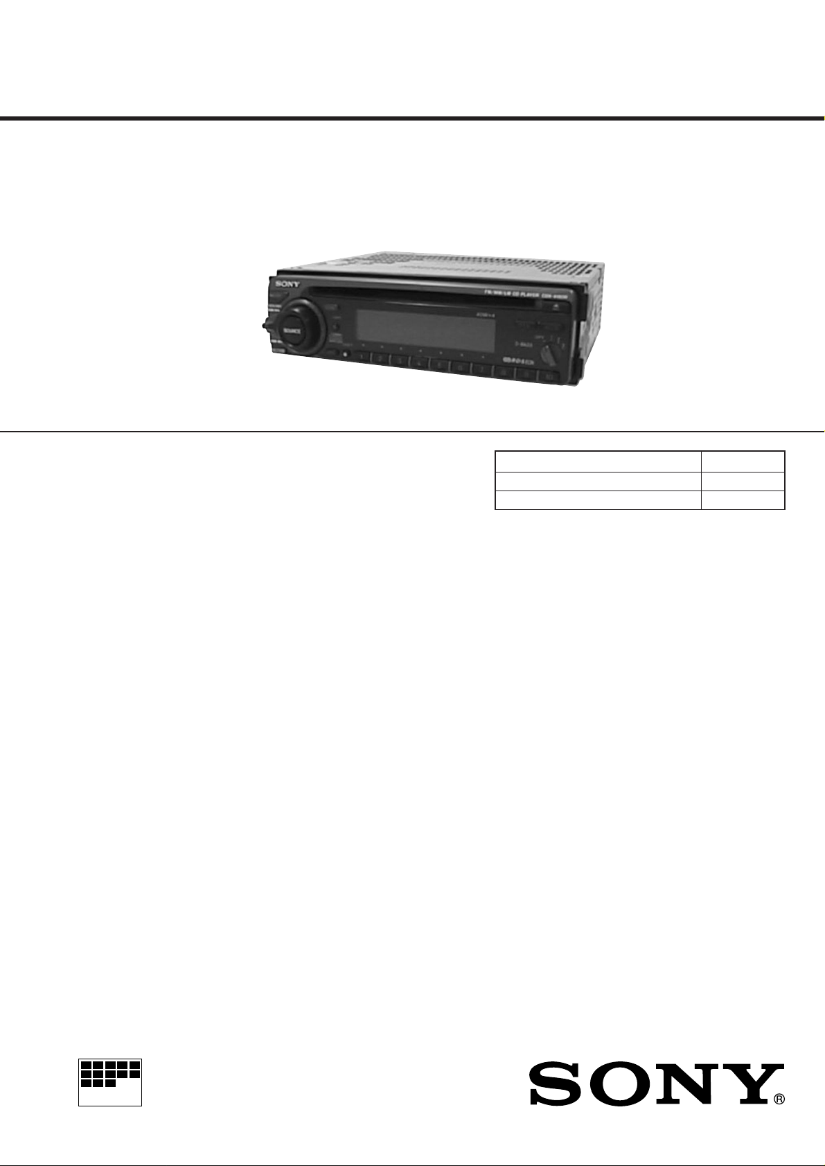
CDX-4180R
SERVICE MANUAL
SPECIFICATIONS
AEP Model
UK Model
Model Name Using Similar Mechanism CDX-4170R
CD Drive Mechanism Type MG-363X-121
Optical Pick-up Name KSS-521A
CD player section
System Compact disc digital audio
system
Signal-to-noise ratio 90 dB
Frequency response 10 - 20,000 Hz
Wow and flutter Below measurable limit
Tuner section
FM
Tuning range 87.5 - 108.0 MHz
Aerial terminal External aerial connector
Intermediate frequency 10.7 MHz
Usable sensitivity 8 dBf
Selectivity 75 dB at 400 kHz
Signal-to-noise ratio 65 dB (stereo),
68 dB (mono)
Harmonic distortion at 1 kHz
0.5% (stereo),
0.3% (mono)
Separation 35 dB at 1 kHz
Frequency response 30 - 15,000 Hz
Capture ratio 2 dB
MW/LW
Tuning range MW: 531 - 1,602 kHz
LW: 153 - 281 kHz
Aerial terminal External aerial connector
Intermediate frequency 10.71 MHz/450 kHz
Sensitivity MW: 30 µV
LW: 50 µV
Power amplifier section
Outputs Speaker outputs
(sure seal connectors)
Speaker impedance 4 - 8 ohms
Maximum power output 40 W × 4 (at 4 ohms)
General
Outputs Line outputs (2)
Power aerial relay control
lead
Power amplifier control
lead
Telephone ATT control
lead
Tone controls Bass ± 10 dB at 100 Hz
Treble ± 10 dB at 10 kHz
Power requirements 12 V DC car battery
(negative ground)
Dimensions Approx. 178 × 50 × 185 mm
(w/h/d)
Mounting dimensions Approx. 182 × 53 × 162 mm
(w/h/d)
Mass Approx. 1.2 kg
Supplied accessories Parts for installation and
connections (1 set)
Front panel case (1)
Design and specifications are subject to change without
notice.
MICROFILM
FM/MW/LW COMPACT DISC PLAYER
– 1 –

SERVICE NOTE
TABLE OF CONTENTS
CAUTION
Use of controls or adjustments or performance of procedures other than those specified herein may result in hazardous radiation exposure.
Notes on Chip Component Replacement
• Never reuse a disconnected chip component.
• Notice that the minus side of a tantalum capacitor may be dam-
aged by heat.
NOTES ON HANDLING THE OPTICAL PICK-UP BLOCK OR
BASE UNIT
The laser diode in the optical pick-up block may suffer electrostatic
breakdown because of the potential difference generated by the
charged electrostatic load, etc. on clothing and the human body.
During repair, pay attention to electrostatic breakdown and also use
the procedure in the printed matter which is included in the repair
parts.
The flexible board is easily damaged and should be handled with
care.
NOTES ON LASER DIODE EMISSION CHECK
The laser beam on this model is concentrated so as to be focused on
the disc reflective surface by the objecti ve lens in the optical pic k-up
block. Therefore, when checking the laser diode emission, observe
from more than 30 cm away from the objective lens.
1. GENERAL
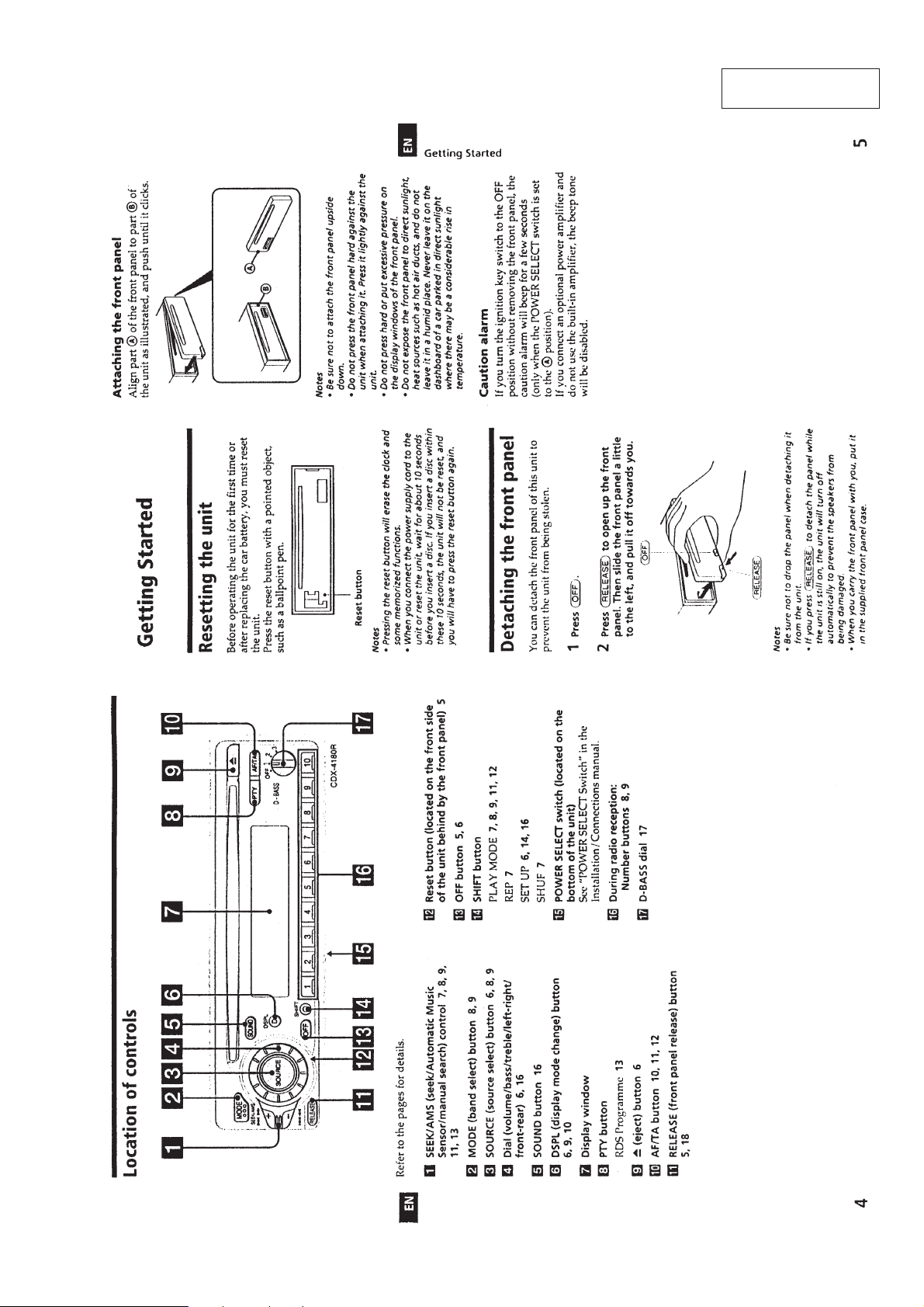
Location of Controls................................................................ 3
Getting Started......................................................................... 3
Setting the Clock .....................................................................4
CD Player ................................................................................4
Radio ....................................................................................... 5
RDS ......................................................................................... 6
Other Functions ....................................................................... 8
Connections ........................................................................... 10
2. DISASSEMBLY
2-1. Cover Assy ........................................................................ 12
2-2. Front Panel Assy ............................................................... 12
2-3. Sub Panel (1) Assy ............................................................ 13
2-4. CD Mechanism Block ....................................................... 13
2-5. Main Board ....................................................................... 14
2-6. Heat Sink ........................................................................... 14
2-7. Chassis (T) Sub Assy ........................................................ 15
2-8. Lever Assy ......................................................................... 15
2-9. Servo Board....................................................................... 16
2-10. Roller Assy........................................................................ 16
2-11. Chassis (OP) (O/S) Assy ................................................... 17
2-12. Optical Pick-up Block ....................................................... 17
3. ELECTRICAL ADJUSTMENTS
Tuner Section.........................................................................18
CD Section ............................................................................ 21
NOTES ON PICK-UP FLEXIBLE BOARD
The pick-up flexible board in this set is secured to the optical pick-up
with an adhesive tape. Once the tape is remov ed, an adhering force
becomes weak, and it cannot be reused.
Therefore, if the optical pick-up is replaced, replace also the pick-up
flexible board with a new one.
SAFETY-RELATED COMPONENT WARNING!!
COMPONENTS IDENTIFIED BY MARK ! OR DOTTED LINE
WITH MARK ! ON THE SCHEMATIC DIAGRAMS AND IN
THE PARTS LIST ARE CRITICAL TO SAFE OPERATION.
REPLACE THESE COMPONENTS WITH SONY P ARTS WHOSE
P AR T NUMBERS APPEAR AS SHO WN IN THIS MANUAL OR
IN SUPPLEMENTS PUBLISHED BY SONY.
4. DIAGRAMS
4-1. IC Pin Description............................................................. 22
4-2. Block Diagram –CD Section–........................................... 25
4-3. Block Diagram –Main Section–........................................ 27
4-4. Circuit Boards Location .................................................... 29
4-5. Schematic Diagram –CD Mechanism Section– ................ 31
4-6. Printed Wiring Boards –CD Mechanism Section–............ 33
4-7. Printed Wiring Board –Main Section– .............................. 35
4-8. Schematic Diagram –Main Section–................................. 39
4-9. Printed Wiring Board –Display Section– .......................... 43
4-10. Schematic Diagram –Display Section–............................. 45
5. EXPLODED VIEWS
5-1. Chassis Section ................................................................. 51
5-2. Front Panel Section ........................................................... 52
5-3. CD Mechanism Section (1) ............................................... 53
5-4. CD Mechanism Section (2) ............................................... 54
5-5. CD Mechanism Section (3) ............................................... 55
6. ELECTRICAL PARTS LIST.........................................56
– 2 –
SECTION 1
GENERAL
This section extracted
from instruction manual.
– 3 –
– 4 –
– 5 –
– 6 –
– 7 –
– 8 –
– 9 –
– 10 –
– 11 –
SECTION 2
DISASSEMBLY
Note : Follow the disassembly procedure in the n umerical order given.
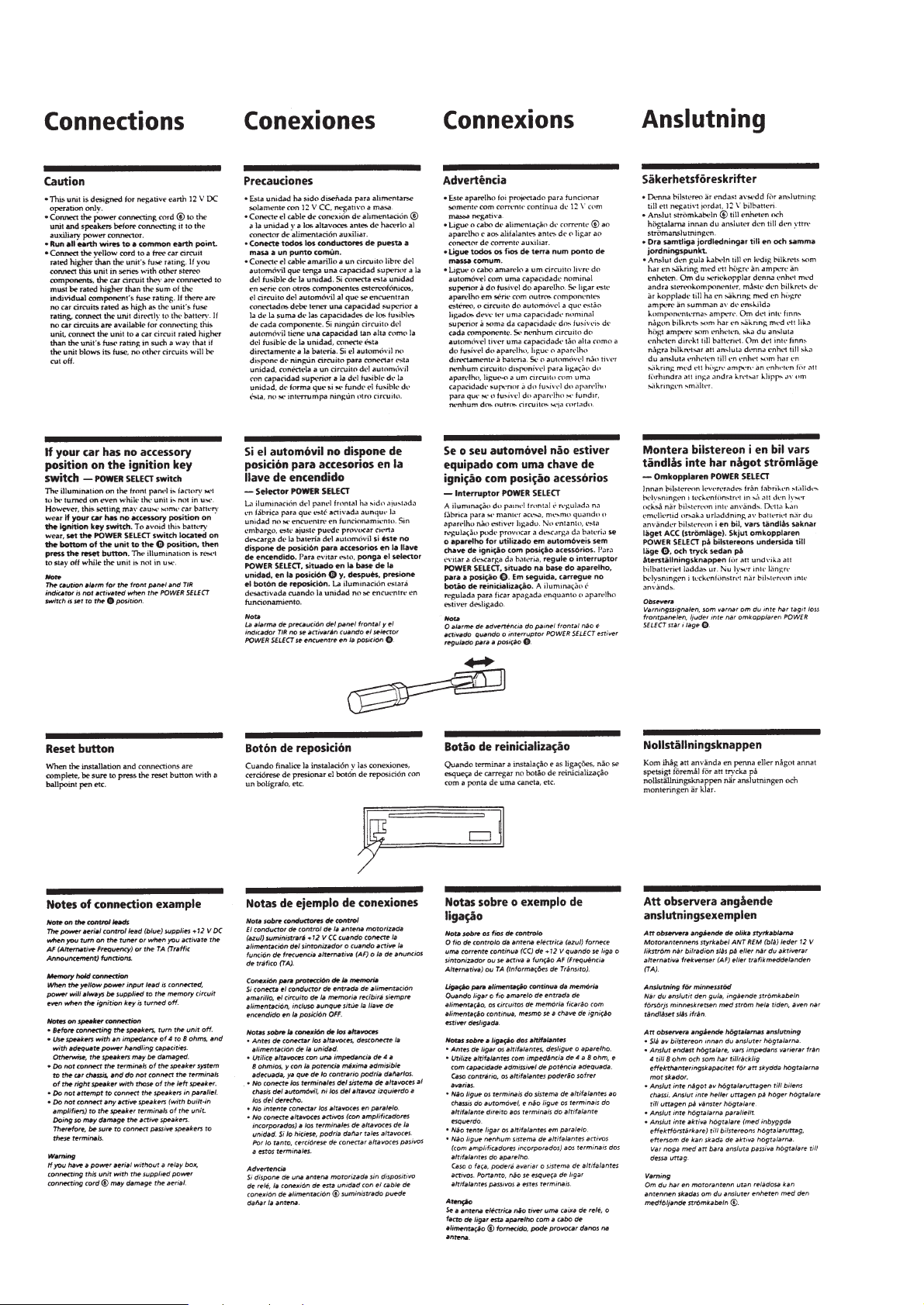
2-1. COVER ASSY
1
claw
3
claws
4
cover assy
2
claw
2-2. FRONT PANEL ASSY
1
button (release)
2
front panel assy
– 12 –
2-3. SUB PANEL (1) ASSY
5
1
PTT 2.6x6
sub panel (1) assy
3
claw
4
claw
2
PTT 2.6x6
2-4. CD MECHANISM BLOCK
8
5
CD mechanism block
2
PTT 2.6x6
bracket (M/D)
7
PTT 2.6x6
4
CNP700
3
PTT 2.6x6
6
PTT 2.6x6
1
PTT 2.6x6
– 13 –
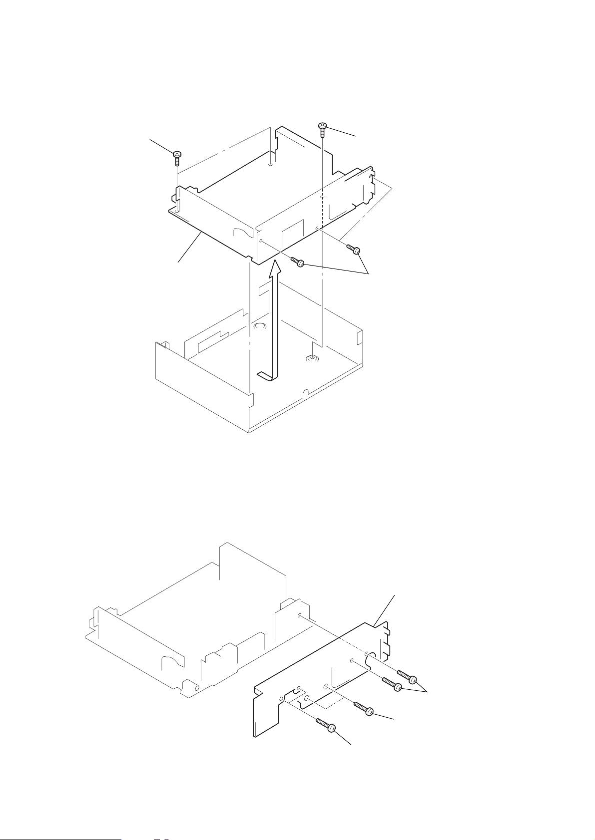
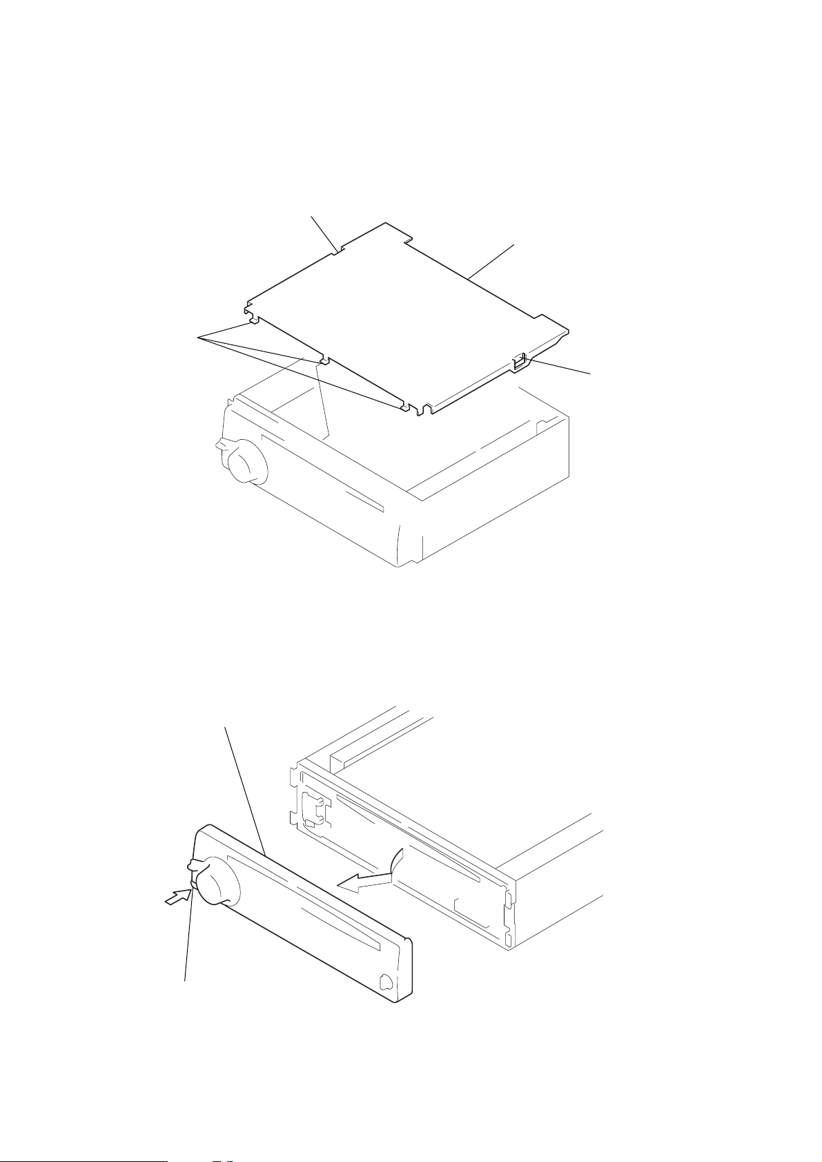
2-5. MAIN BOARD
3
ground point screws
4
MAIN board
2
ground point screw
1
PTT 2.6x8
2-6. HEAT SINK
1
PTT 2.6x8
4
heat sink
2
PTT 2.6x10
3
PTT 2.6x8
– 14 –
2-7. CHASSIS (T) SUB ASSY
1
Unsolder the
lead wires.
red
white
black
3
P 2x3
2
P 2x3
4
chassis (T) sub assy
2-8. LEVER ASSY
6
lever (R) assy
3
tension spring (LR)
7
lever (L) assy
5
guide (disc)
1
PS 2x4
2
DISC IN SW board
4
claws
– 15 –
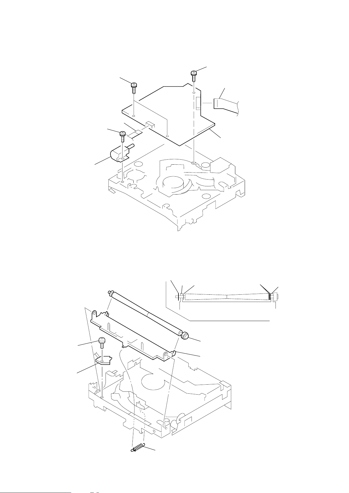
2-9. SERVO BOARD
4
5
PS 2x4
1
3
P 2x3
loading motor assy
CN3
6
PS 2x4
2
CN2
7
SERVO board
2-10. ROLLER ASSY
• When installing, take note of the positions
arm (roller) and washers. (Fig. 1)
4
PS 2x3
5
LOAD SW board
washer
arm
washer
3
2
Fig. 1
roller assy
arm (roller)
washers
arm
1
tension spring (RA)
– 16 –

2-11. CHASSIS (OP) (O/S) ASSY
8
compression spring (FL)
1
tension spring (angle)
7
9
compression spring (FL)
2
tension spring (KR1)
5
Fit lever (D) in the
direction of the arrow.
chassis (OP) (O/S) assy
6
Turn loading ring in the
direction of the arrow.
4
damper (T)
2-12. OPTICAL PICK-UP BLOCK
1
P 2x3
2
sled motor assy
3
damper (T)
3
optical pick-up block
– 17 –

SECTION 3
ELECTRICAL ADJUSTMENTS
TUNER SECTION
0 dB = 1 µV
Cautions during repair
When the tuner unit is defective, replace it by a new one
because its internal block is difficult to repair.
TEST MODE
This set have the test mode function. In the test mode, FM Auto
Scan/Stop Level and MW Auto Scan/Stop Level adjustments can
be performed easier than it in ordinary procedure.
<Set the Test Mode>
1. Set the “OFF” mode.
2. Push the preset 4 button.
3. Push the preset 5 button.
4. Press the preset 1 button for more than two seconds.
5. Then the display indicates all lights, the test mode is set.
<Release the Test Mode>
1. Push the OFF button.
Note on Adjustment
The adjustments of tuner section, should be performed according
to the following sequence.
1. FM Auto Scan/Stop Level Adjustment
2. FM Stereo Separation Adjustment
3. FM RDS S-Meter Adjustment
4. MW Auto Scan/Stop Level Adjustment
FM Auto Scan/Stop Level Adjustment
Setting :
D-BASS switch : OFF
SOURCE button: FM
FM RF signal
generator
antenna
0.01 µF
Carrier frequency : 98.00 MHz
Output level : 22 dB (12.6 µV)
Mode : mono
Modulation : 1 kHz, 22.5 kHz deviation (30%)
terminal
Procedure :
1. Set to the test mode.
2. Push the SOURCE button and set to FM.
Display
SHUF
REG
3. Push the preset 3 button.
Display
SHUF
set
REG
4. Adjust with the volume R V2 on TU1 so that the “FM” indication
turns to “FM0” indication on the display window.
But, in case of already indicated “FM0”, turn the RV2 so that
put out light “0” indication and adjustment.
Display
SHUF
REG
Adjustment Location : See page 20.
– 18 –

FM Stereo Separation Adjustment
REG
SHUF
Setting :
D-BASS switch : OFF
SOURCE button : FM
FM RDS S-Meter Adjustment
Setting :
D-BASS switch : OFF
SOURCE button : FM
FM RF signal
generator
0.01 µF
Carrier frequency : 98.00 MHz
Output level : 70 dB (3.2 mV)
Mode : stereo
Modulation : main : 1 kHz, 20 kHz deviation (26.5%)
sub : 1 kHz, 20 kHz deviation (26.5%)
19 kHz pilot : 7.5 kHz deviation (10%)
antenna
terminal
set
10 k
Ω
LINE OUT REAR
Procedure :
FM stereo
signal generator
output channel
Level meter Level meter
connection reading (dB)
L-CH L-CH A
B
R-CH L-CH Adjust RV4 on TU1 for
minimum reading.
R-CH R-CH C
D
L-CH R-CH Adjust RV4 on TU1 for
minimum reading.
L-CH stereo separation : A – B
R-CH stereo separation : C – D
The separations of both channels should be equal.
level meter
FM RF signal
generator
antenna
0.01 µF
Carrier frequency : 98.00 MHz
Output level : 35 dB (56.2 µV)
Mode : mono
Modulation : no modulation
terminal
set
Procedure :
1. Set to the test mode. (See page 18.)
2. Push the SOURCE button and set to FM.
Display
SHUF
REG
3. Push the preset 10 button.
4. Adjust RV801 so that the display indication is “16.0”.
Display
Specification : Display indication : 15.8 to 16.2
Adjustment Location : See page 20.
Specification : Separation more than 28 dB
Adjustment Location : See page 20.
– 19 –

MW Auto Scan/Stop Level Adjustment
Setting :
D-BASS switch : OFF
SOURCE n MODE button : MW
AM RF signal
generator
AM dummy
antenna (50 Ω)
30
15 pF
Ω
65 pF
set
Adjustment Location : tuner unit (TU1)
–set upper view–
Carrier frequency : 999 kHz
30% amplitude
antenna
terminal
modulation by
1 kHz signal
output level : 33 dB (44.7 µV)
Procedure :
1. Set to the test mode. (See page 18.)
2. Push the SOURCE button.
3. Push the MODE button and set to MW.
Display
SHUF
REG
TP
4. Push the preset 3 button.
Display
SHUF
REG
TP
5. Adjust with the volume RV1 on TU1 so that the “MW”
indication turns to “MW0” indication on the display window.
But, in case of already indicated “MW0”, turn the RV1 so that
put out light “0” indication and adjustment.
Display
SHUF
TU1
RV1
MW AUTO SCAN/
STOP LEVEL ADJ
RV2
FM AUTO SCAN/
STOP LEVEL ADJ
RV801
FM RDS
S-METER ADJ
RV4
FM STEREO
SEPARATION ADJ
REG
TP
Adjustment Location : tuner unit (TU1)
– 20 –

CD SECTION
Note:
1. CD Block basically constructed to operate without adjustment.
Therefore, check each item in order given.
2. Use YEDS-18 disc (3-702-101-01) unless otherwise indicated.
3. Use the oscilloscope with more than 10 MΩ impedance.
4. Clean an objective lens by an applicator with neutral detergent
when the signal level is low than specif ied value with the f ollowing
checks.
Focus Bias Adjustment
Setting: This adjustment is performed with the set placed
horizontally.
oscilloscope
SERVO board
TP (RF)
TP (RF. GND)
Procedure:
1. Connect an oscilloscope between TP (RF) and TP (RF. GND)
on the SERVO board.
2. Connect the power supply.
3. Push the RESET button (S900) on the MAIN board.
4. Insert the disc (YEDS-18) and playback.
5. Adjust RV1 so that the oscilloscope w aveform is clear and check
RF signal level is correct or not.
Note: Clear RF signal waveform means that the sharp “≈ ” can be
clearly distinguished at the center of the waveform.
Focus Gain Adjustment (Coarse adjustment)
This adjustment is not required unless the following parts are re placed:
• Optical pick-up
•RV4
Procedure:
1. Set RV4 to the standard position. (mechanical center)
2. Check whether operation noise (while noise type) caused by
the 2-axis device (lens section of the optical pick-up) is
abnormally loud.
If the operation noise is too loud, turn RV4 slightly counterclockwise.
• If the gain is too low:
Focus does not function and no music is selected.
• If the gain is too high:
Noise caused by scratches and dust is heard and the operation
becomes unstable.
Adjustment Location: servo board
Adjustment Location: servo board (component side)
FOCUS GAIN ADJ
IC3
CN2
RV4
RF signal waveform
VOLT/DIV: 200 mV
TIME/DIV: 500 nS
level: 1.0 – 1.5 Vp-p
• When observing the eye pattern, set the oscilloscope to AC range
and raise the vertical sensitivity so that it may be easily seen.
Adjustment Location: servo board
CN1
IC1
TP
(RF. GND)
IC2
TP
(RF)
CN3
RV1
FOCUS BIAS ADJ
– 21 –

SECTION 4
DIAGRAMS
4-1. IC PIN DESCRIPTION
• IC801 MB90574FPV-G-110 (SYSTEM CONTROL)
Pin No. Pin Name I/O Pin Description
1 LD ON O Laser power ON/OFF control pin
2 FOK I Focus signal detection input
3 XLAT25 O CD signal process latch output
4 DATA25 O CD signal process serial data output
5 XRSRO O CD signal process IC reset output
6 GFS I GFS signal detection input
7 NIL — Not used. (Contact to GND.)
8 VCC — Power supply (+5 V)
9 PLL SI I PLL data input
10 PLL SO O PLL data output
11 PLL CKO O PLL CLK output
12 NOSE I Front panel connect detection input
13 LCD SO O LCD serial data output
14 LCD CKO O LCD serial clock output
15 BEEP O Buzzer control output
16 DBMOD2 O D-BASS mode set signal output
17 SQSI I SUBQ data input
18 NIL — Not used. (Contact to GND.)
19 SQCKO O SUBQ read clock output
20 UNI SI I BUS system serial interface input
21 UNI SO O BUS system serial interface output
22 UNI CKI/O I/O BUS system serial interface input/output
23 C OUT I CD track jump number count input
24 SIRCS I Remote commander input
25 SRDT I CD-TEXT data input
26 NIL — Not used. (Contact to GND.)
27 SCLK O CD TEXT data read clock output (Not used.)
28 CLOCK25 O CD signal process serial clock output
29 SYSRST O System reset control output
30 DEEM O Emphasis control output
31 DBMOD1 O D-BASS mode set signal output
32 MD ON O Machanism deck section power supply control output
33 VSS — GND
34 C — Capacitor terminal for power supply
35 CD ON O CD power supply control output
36 BUS ON O BUS ON control output (Not used.)
37 AD ON O Power control output for A/D conversion
38 DVCC — Power supply for D/A convertor
39 DVSS — GND for D/A convertor
40 TEST I Test mode direct setting input
41 VOL CE O Electric volume serial chip enable output
42 AVCC — Power supply for analog circuit
43 AVRH — Pow er supply for A/D convertor
44 AVRL — Power supply for A/D convertor
45 A VSS — GND for analog circuit
46 KEY IN0 I Key input
47 KEY IN1 I Key input
48 KEY IN2 I Key input for D-BASS rotary switch
49 RC IN0 I Rotary commander input
50, 51 NIL — Not used. (Contact to GND.)
52 MPDH I Tuner multi-path input
– 22 –

Pin No. Pin Name I/O Pin Description
53 S-METER I S-meter voltage detection input
54 VCC — Power supply
55 AMP MUTE O Power amplifier mute control output
56 AMP ON O Power amplifier power control output
57 XMODE O Reset signal output for CD-TEXT decoder (Not used.)
58 VOL SO O Electric volume serial data output
59 VOL CKO O Electric volume serial clock output
60 AU MUTE O Audio mute signal output
61 AF MUTE O RDS mute signal output (Not used.)
62 TU MUTE O Tuner mute signal output
63 VSS — GND
64 ACC IN I Accessory power voltage detection input
65 AFSEEK O RDS operation control output
66 M SIO I/O EEPROM serial data input/output (Not used.)
67 DAVN I RDS data input detection input
68 M CK O EEPROM serial clock output (Not used.)
69 M CE O EEPROM chip enable output (Not used.)
70 RDS SI O RDS serial data input
71 RDS CKI O RDS serial clock input
72 RC IN1 I Remote commander shift key input
73 X1A — Low frequency oscillator input
74 X0A — Low frequency oscillator input
75 SCOR I SCOR signal detection input
76 BU IN I Back-up power supply detection input
77 DQSY I CD-TEXT data set complete signal detection input (Not used.)
78 CD SENCE I CD SENS signal detection input
79 KEY ACK I Key input acknowledge
80 TEL MUTE I Telephone mute detection input
81 ST IN/MONO I Tuner stereo signal detection input
82 SEEKOUT O SEEK OUT output
83 SD IN I Signal detection input
84 NC — Not used. (Contact to GND.)
85 PLL CE O PLL CE output
86 H I Hardware standby input
87 VSS — GND
88, 89 VCC — Power supply
90 RESET I Reset input
91 VSS — GND
92 X0 — High frequency oscillator input
93 X1 — High frequency oscillator input
94 VCC — Power supply
95 PW SEL I Power select initial setting input
96 NIL — Not used. (Contact to GND.)
97 AREA1 I Fixed to “L”.
98 AREA2 I Fixed to “L”.
99 AREA3 I US, Canadian model : Fixed to “L”. E model : Fixed to “H”.
100 BAND (9K 10K) I AM/FM frequency select (E model)
101 NIL — Not used. (Contact to GND.)
102 PH3 I Disc insert detection photo sensor input (Not used.)
103 PH2 I Disc insert detection photo sensor input (Not used.)
104 LCD CE O LCD chip enable output
105 NIL — Not used. (Contact to GND.)
106 RE0 I Rotary encoder input
– 23 –

Pin No. Pin Name I/O Pin Description
107 RE1 I Rotary encoder input
108 LAMP ON O Illumination power control output
109 PW ON O System power control output
110 REGMOD1 O FM power control output
111 REGMOD2 O System power control output
112 CTL1 O Laser power ON/OFF control output (Not used)
113 CTL2 O Laser power ON/OFF control output
114 FWD O Loading motor control output (Loading)
115 REV O Loading motor control output (Eject)
116 L SW I SLED limit switch detection input
117 IN SW I Disc insert detection input
118 D SW I DOWN switch detection input
119 VSS — GND
120 SELF SW I SELF switch detection input
– 24 –

4-2. BLOCK DIAGRAM — CD SECTION —
CDX-4180R
OPTICAL PICK-UP
KSS-520A
I-V
CONV.
PD
LD
TRACKING
FOCUS
RV1
FOCUS BIAS
RV4
FOCUS GAIN
LD DRIVE
SERVO 5V
M902
(SLED)
M901
(SPINDLE)
M903
(LOADING)
Q2
RF AMP, SERVO CONTROL
35 PD1
36 PD2
39 E
38 F
SERVO 5V
37 FE BIAS
1 FEO
2 FEI
34 PD
33 LD
Q1
FOCUS/TRACKING COIL DRIVE,
16 CH2+
15 CH2-
18 CH1+
17 CH1-
13 CH3+
M
14 CH3-
12 CH4+
M
11 COM
M
10 CH5+
IC2
MOTOR DRIVE
IC3
DIGITAL SIGNAL
PROCESSOR
IC1
31RFO
19CLK
20XLT
21DATA
22XRST
23C. OUT
24SENS
25FOK
16SLO
13TAO
6FEO
19CH1 IN
22CH2 IN
24CH3 IN
3CH4 IN
7REW
6FWD
5CTL2
4CTL1
14 RF
59 CLKO
57 XLTO
56 DATO
50 XRST
55 CNIN
54 SEIN
1 FOK
3 MDP
SERVO 5V
SCOR
21PCMD
20LRCK
22BCK
34XTAI
27GFS
46SQSO
47SQCK
49SENS
51DATA
52XLAT
53CLOK
43
3DI
1 LRCI
2 BCKI
4 CLK
6 RSTN
16
DB/DS
D-BASS
CONTROL
IC701
MOD1
MOD2
D/A CONVERTER
IC702
9DOUT
10BCKO
11LRCO
X700
16.9344MHz
14
15
6DI
5 BCKI
8 LRCI
3 CLKO
18 XTI
19 XTO
12LO
14RO R-CH
2DEEM
22RSTN
SYSTEM CONTROL
IC801(1/2)
30 DEEM
31 DBMOD1
16
DBMOD2
6 GFS
17 SQSI
19 SQCKO
78 CD SENCE
4 DATA25
3 XLAT25
28 CLOK25
75 SCOR
5 XRSRO
2 FOK
23 C OUT
1 LD ON
115 RE V
114 FW D
113 CTL2
57 XMODE
27 SCLK
25 SRDT
77 DQSY
1
MAIN
SECTION
SW1
(DISC IN)
SW2
(SELF)
SW3
Signal path
: CD
04
(LIMIT)
SW4
(DOWN)
CD 5V
SERVO 5V
MD 8V
SERVO 5V
REG
Q913
CD 5V
REG
Q909
MD 8V
REG
Q912
MD 8V
SWITCH
Q910, 911
BACK UP
CD POWER
SWITCH
Q907,908
117 IN SW
120 SELF SW
116 L SW
118 D SW
CD ON
3235MD ON
– 25 – – 26 –

CDX-4180R
4-3. BLOCK DIAGRAM — MAIN SECTION —
CNJ600
(ANT)
Signal path
: FM
: MW
: CD
1
2
AM ANT
FM ANT
TUNER UNIT
TU1
FM L-CH
FM R-CH
AM DET
LO/DX
AM-IFC
FM-IFC
ST-IND
S-METER
FM-DET
18
16
12
4
11
21
VCO
6
5
VT
SD
20
SEEK
13 82
22
19
23
8
FM+B
9
TU+B
10
AM+B
TUNER LINE SWITCH
IC404(1/2)
8
TU 5V
R-CH
R-CH
VT
CONTROL
Q611
6
1
VT
SWITCH
IC603
FM8V
D601
TU 5V REG
D602
AM8V
6
3
7
RV801
S-METER
TU5V
Q601
BACK UP LINE
9
FM8V
IC404(2/2)
1
AM 8V
5
2
2
13
HPF
HPF
Q610
S-METER
BUFFER
Q801
B+ SWITCH
Q604, 605
TU5V
13
15
16
18
20
16
14
U COM 5V
COM+B REG
Q903
SWITCH
Q901,902
CD
MUTE
Q607
PLL
IC601
IC602
COM+B
1
DIN
CLK
DOUT
X OUT
X IN
CLK
DATA
DAVN
XI
XO
MPDH
RESET
2 1
IC902
SECTION
LO/DX
9
IFIN
AMOSC
FMOSC
PD
RDS DEMODULATOR
SMETER
FM-DET
AVDD
MUTE
SWITCH
Q701
5
4
6
20
X601
7.2MHz
1
X801
32.768kHz
10
9
8
5
X602
4
4.332MHz
2 4
S900
RESET
SYSTEM CONTROL
IC801(2/2)
TU MUTE
62
PLL SO
10
11
PLL CKO
PLLSI
9
73
X1A
X0A
74
65
AF SEEK
83
SD IN
SEEK OUT
ST IN/MONO
81
53
S-METER
PLL SO
10
11
PLL CKO
PLLSI
9
MPDH
RESET
90
LAMP ON
108
VOL CKO
VOL SO
VOL CE
BEEP
AF MUTE
AU MUTE
AMP MUTE
AMP ON
LCD CE
LCD CKO
LCD SO
NOSE
RC IN0
RC IN1
KEY IN1
KEY IN2
AD ON
AVRH
KEY ACK
KEY IN0
RE0
RE1
TEL MUTE
ACC IN
-3
L
ELECTRONIC VOLUME
IC401
L4
35
L3
36
L2
37
L1
38
59
58
41
15
61
60
55
56
104
14
13
X0
92
93
X1
12
49
72
47
48
37
43
79
46
106
107
80
64
D918
CLDICE
X800
4.19MHz
181716
TONE
D801
FLOUT
21
20
RLOUT
MUTE
Q110
MUTE
SWITCH
Q401
Q402
+
62
63
64
D919
LCD DRIVE
IC801
CE
CLK
DATA
P2/S2
CNP802
(REMOTE IN)
KEY ACTIVE
Q914,915
BACK UP
2
POWER SUPPLY
MUTE
Q111
LCD801
(DISPLAY BOARD)
IC901
PL801
PL802
KEY MATRIX
LSW801-819, S802
D-BASS
SWITCH
S801
ROTARY
ENCODER
RE801
LAMP REG
Q802, 805
POWER AMP
IC200
FL
12
RL
11
COM +8V
TEL MUTE
SWITCH
Q916
22 4
5
3
9
7
MUTE
STBY
LSW801-819
LED801-805
CHECK
R-CH
R-CH
ACC
Q905
-4
-5
-6
CNP501
10
12
R-CH
11
13
D906
FRONT
R
L
R
1
FL+
9
FL-
2
RL+
RL-
4
FR+
FR-
3
RR+
RR-
ATT
7
ACC
PJ400
LINE OUT
REAR
10
11
2
3
4
5
9
MODE2
MODE1
STBY
BU5V
COM8V
AM8V
FM8V
VCC
AMP+B
ANT+B
7
6
8
BACK UP LINE
BACK UP LINE
F901
16
BATT
5
AMP REM
6
ANT REM
15
TEST
111
REGMOD2
REGMOD1
PW ON
PW SEL
TEST
110
109
95
40
SW801
(POWER SELECT)
OFF
ON
U COM 5V
PULL UP 5V
COM+8V
AM8V
FM8V
BACK UP LINE
04
D807
BACK UP LINE
D910
ACC DET
SWITCH
Q917, 918
BATT
CHECK
Q906
BU IN
76
– 27 – – 28 –

4-4. CIRCUIT BOARDS LOCATION
tuner unit
(TU1)
DISPLAY board
LOAD SW board
DISC IN SW board
SUB board
LIMIT SW board
MAIN board
SERVO board
– 29 –

• Waveforms (MODE:PLAY)
1
0V
Approx. 620mVp-p
1
(FEO)
IC2
2
1.2Vp-p
3
4
5
6
7
IC2
Approx. 200mVp-p
IC2
IC1
IC1
IC1
IC1
(RFO)
#¡
(TEO)
$™
(MDP)
3
22.7µsec
(LRCK)
@º
474nsec
(BCK)
@™
16.89MHz
(XTAI)
#¢
2.6Vp-p
7.6µsec
5.8Vp-p
5.7Vp-p
3.2Vp-p
0V
Note on Schematic Diagram:
• All capacitors are in µF unless otherwise noted. pF: µµF
50 WV or less are not indicated except for electrolytics
and tantalums.
• All resistors are in Ω and 1/
specified.
Note: The components identified by mark ! or dotted line
with mark ! are critical for safety.
Replace only with part number specified.
• U : B+ Line.
• H : adjustment for repair.
• Power voltage is dc 14.4V and fed with regulated dc power
supply from ACC and BATT cords.
• Voltage and waveforms are dc with respect to ground
under no-signal conditions.
no mark : CD PLAY
• V oltages are taken with a VOM (Input impedance 10 M Ω).
Voltage var iations may be noted due to normal production
tolerances.
• Waveforms are taken with a oscilloscope.
Voltage var iations may be noted due to normal production
tolerances.
• Circled numbers refer to waveforms.
• Signal path.
J : CD
: Impossible to measure
∗
4
W or less unless otherwise
– 30 –


• IC Block Diagrams
IC1 CXD2507AQ
FOK
MON
MDP
MDS
LOCK
TEST
FILO
FILI
PCO
VSS
AVSS
CLTV
AVDD
BIAS
ASYI
ASYO
ASYE
WDCK
XLON
SPOC
SPOD
63
62
64
1
2
3
4
5
6
7
8
9
10
11
12
13
RF
14
15
16
17
18
19
SERVO AUTO
SEQUENCER
CPU
INTERFACE
14
DIGITAL
PLL
ASYMMETRY
CORRECTOR
5
20 21 22 23 24 25 26 27 293031 3228
LRCK
PCMD
BCLK
16K
RAM
GTOP
VDD
CLKO
SPOB
SPOA
58596061
5
SUB CODE
PROCESSOR
EFM
DEMODULATOR
3
ERROR
CORRECTOR
GFS
VDD
XUGF
XPCK
XLTO
DATO
5657
4
D/A
INTERFACE
3
C2PO
RFCK
CNIN
XROF
5455
MNT3
SEIN
53
6
CLOK
52
MNT1
XLAT
DIGITAL
CLV
DIGITAL
OUT
CLOCK
GENERATOR
51
DATA
50
XRST
49
SENS
48
MUTE
47
SQCK
SQSO
46
45
EXCK
44
SBSO
43
SCOR
42
VSS
41
WFCK
40
EMPH
39
DOUT
C4M
38
37
FSTT
36
XTSL
35
XTAO
34
XTAI
MNTO
33
IC3 BA6796FP-T1
OP IN –
OP IN +
VREF
28
1
OPOUT
26
27
CTL1 CTL2 FWD REV
23 4
CH4
CH4-IN
CH3
THERMAL
SHUT
DOWN
CTL1
2425
LOGIC
5
CTL2
CH3-IN
LEVEL
SHIFT
CH2
23
78
6
FWD
REV
22
CH2-IN
LEVEL
SHIFT
V/I
TRAY
21
VCC
LEVEL
SHIFT
VCC
DRIVE
BUFFER
9
10
GND
CH1
CH5 –
1920
CH1-IN
DRIVE
BUFFER
DRIVE
BUFFER
11
CH1 +
LEVEL
SHIFT
COM
CH1 –
DRIVE
BUFFER
DRIVE
BUFFER
12 13
CH4 +
161718
DRIVE
BUFFER
DRIVE
BUFFER
CH3 +
CH2 +
15
DRIVE
BUFFER
DRIVE
BUFFER
14
CH2 –
CH3 –
– 47 –

IC2 CXA1782BQ
FE BIAS
PHD 2
36 35 34
37
F
38
E
39
PHD 1
RF IV AMP1
RF IV AMP2
APC
F IV AMP
PHD
33
FE AMP
LD
RF M
32
LEVEL S
FOK
RF O
31
TTL
IIL
FZC COMP
RF I
30 29 28 27 26 25
MIRR
IIL DATA REGISTER
TOG1-3
FS1-4 TG1-2 TM1-7 PS1-4
BAL1-3
CP
DFCT
INPUT SHIFT REGISTER
ADDRESS DECODER
OUTPUT DECODER
CB
CC1
IIL
TTL
TTL
IIL
CC2
FOK
24
SENS
C.OUT
23
XRST
22
21
DATA
20
XLT
19
CLK
VCC
18
VEE
TED
LPFI
TEI
ATSC
TZC
TDFCT
BAL2
TOG1
WINDOW COMP
BAL 3
TOG2
E IV AMP
TOG3
ATSC
TE AMP
HPF COMP
TZC COMP
DFCT
TM1
DFCT
FS4
2
1
FEI
FEO
FDFCT
43
FGD
LPF COMP
TG1
FCS PHASE
COMPENSATION
5
6
FLB
FE O
FS1
FS2
FE M
TRACKING
PHASE
COMPENSATION
TM6
TM5
TM4
TM3
TM7
TG2
987
TGU
SRCH
ISET
TM2
F SET
11
10
TG2
FSET
ISET
17
SL O
16
SL M
15
SL P
14
13
TA O
12
TA M
EI
40
BAL1
41
42
43
44
45
46
47
VC
48
– 48 –

IC401 LC75374E
34
LSELO
35
L4
L3
36
L2
37
L1
38
39
VDD
R1
40
41
R2
R3
42
R4
43
44
RSELO
LVRIN
1
RVRIN
LT3
LT2
+
–
–
+
LT1
–
+
+
–
+
–
DECODER LATCH
+
–
RT1
RT2
RT3
LCOM
+
–
+
–
–
+
–
+
2 345 6 7 8 9 10
RCOM
LSIN
LTOUT
CONTROL
REGISTER
RSIN
RTOUT
NC
2627282930313233
SHIFT
NC
LSB2
LSB1
NC
2324
25
22
LFIN
+
–
+
+
–
11
NC
RSB1
RSB2
–
+
–
–
+
–
+
LFOUT
21
LROUT
20
19
VREF
18
CE
17
DI
16
CL
15
VSS
14
RROUT
RFOUT
13
12
RFIN
IC601 BU2624FV
XIN
1
2
CE
4
CK
DA
5
CD
6
7
P0
9
P1
10
P3
CTL
I/O
REFERENCE
DIVIDER
SHIFT REGISTER LATCH
MAIN
COUNT
PRESCALER
IF COUNT
CTL
20BIT COUNT
PHASE
DET
XOUT
20
19
VSS
18
PD
17
VDD
FMIN
16
AMIN
15
P2
14
13
IFIN
12
SD
P4
11
– 49 –

IC702 SM5878AM-E2IC602 SAA6588T
11
PSWN
12
MAD
13
AFIN
14
VDDA
15
VSSA
16
MPX
17
VREF
18
SCOUT
19
CIN
20
LVIN
IC701 SM5852FS-E2
LRCI
1
BCKI
2
INTERFACE
3
DI
4
CLK
5
VSS
SEQUENTIAL
6
RSTN
TESTN
MUTEN
CONTROL
7
8
CONTROL
PAUSE
DETECTOR
CLOCKED
COMPARATOR
POWER SUPPLY
AND RESET
57kHz
8th ORDER
BAND-PASS
INPUT
SYSTEM
CLOCK
MUTE
SIGNAL
QUALITY
DETECTOR
RDS/RDBS
DEMODULATOR
DIGITAL
SIGNAL
PROCESSOR
OUTPUT
INTERFACE
MODE
CONTROL
IIC-BUS
SLAVE
TRANSCEIVER
4
4
INTERFACE
REGISTER
5
RDS/RDBS
DECODER
OSCILLATOR
AND CLOCK
CONTROL
MULTI-PATH
DETECTOR
TEST
10
SCL
9
SDA
1
MUTE
DEEN
2
8
DAVN
7
VDDD
6
VSSD
5
OSCI
OSC0
4
CKO
3
TCON
2
MPTH
1
MRO
DB/DS
16
MOD2
15
MOD1
14
OPT
13
VDD
12
LRCO
11
BCKO
10
DOUT
9
DVSS
BCKI
DVDD
LRCI
TSTN
TO1
AVDDL
3
4
5
DI
6
7
8
9
10
11
LO
12
ATTENUATION COUNTER
FILTER & ATTENUATION
OPERATION BLOCK
R
LPF
AMP
L
OPERATION BLOCK
L
INPUT INTERFACE
11 LEVEL
DEM DAC
NOISE SHAPER
11 LEVEL
DEM DAC
R
11 LEVEL
DEM DAC
LPF
AMP
TIMING
CONTROL
CLOCK
GENERATOR
11 LEVEL
DEM DAC
ATCK
24
MODE
23
RSTN
22
21
DS
20
XVSS
XTO
19
18
XTI
17
XVDD
MUTE
16
15
AVDDR
14
RO
13
AVSS
IC901 BA3918-V3
–
+
2 3
4
1
NC
STB
MODE2
MODE1
REGULATOR
OVER VOLTAGE
PROTECT
–
+
5 6 7 8 9 10 1211
VDD
AMP
VCC
ANT
COM
AM
–
+
– 50 –
–
+
FM
GND

NOTE:
1
11
3
5
12
8
9
6
7
2
10
4
#1
#1
#2
#2
#2
#10
#11
#11
#2
#2
#2
#1
#1
#1
#3
#3
MG-363X-121
TU1
F901
A
A
B
B
• The mechanical parts with no reference
number in the exploded views are not supplied.
• Items marked “*” are not stocked since
they are seldom required for routine service.
Some delay should be anticipated
when ordering these items.
• -XX and -X mean standardized parts, so
they may have some difference from the
original one.
• Abbreviation
G : German model
5-1. CHASSIS SECTION
SECTION 5
EXPLODED VIEWS
• Color Indication of Appearance Parts
Example :
KNOB, BALANCE (WHITE) ... (RED)
• Accessories and packing materials and
hardware (# mark) list are given in
the last of this parts list.
N
Parts Color Cabinet’s Color
N
The components identified by
mark ! or dotted line with mark.
! are critical for safety.
Replace only with part number
specified.
Ref. No. Part No. Description Remark
1 X-3374-926-1 COVER ASSY
2 X-3374-808-1 PANEL (1) ASSY, SUB
3 X-3368-104-2 LOCK ASSY
* 4 3-019-564-01 BRACKET (M/D)
5 3-915-923-01 SCREW, GROUND POINT
Ref. No. Part No. Description Remark
* 8 3-019-565-01 BRACKET (IC)
* 9 3-019-533-01 BRACKET (REG)
* 10 3-020-104-01 CHASSIS (MAIN)
11 1-776-527-61 CORD (WITH CONNECTOR) (ISO) (POWER)
12 3-937-650-01 PLATE (C), GROUND
* 6 A-3294-367-A MAIN BOARD COMPLETE (G)
* 6 A-3294-369-A MAIN BOARD COMPLETE (AEP,UK)
* 7 3-020-107-11 HEAT SINK
F901 1-532-877-11 FUSE (BLADE TYPE) (AUTO FUSE) 10A
TU1 A-3282-029-A TUNER UNIT (TUX-006/2 (E))
– 51 –

5-2. FRONT PANEL SECTION
4
not supplied
(DISPLAY board)
62
57
LCD801
66
58
63
59
53
64
54
D
C
D
65
C
61
60
#4
#4
#
67
51
56
55
52
Ref. No. Part No. Description Remark Ref. No. Part No. Description Remark
51 3-019-549-01 BUTTON (RELEASE)
52 3-019-544-31 KNOB (SEEK/AMS)
53 3-375-373-01 SPRING (RELEASE)
54 3-019-550-01 BUTTON (MODE/SOUND)
55 3-019-528-01 BUTTON (1-10)
56 3-019-551-21 BUTTON (EJECT)
57 3-019-545-01 BUTTON (SOURCE)
58 3-019-547-01 KNOB (VOL)
59 3-019-548-01 RING
60 3-019-543-01 KNOB (D-BASS)
* 61 X-3374-890-1 HOLDER (LCD) ASSY
* 62 3-020-102-01 PLATE (I) (LCD), GROUND
63 3-021-407-01 SHEET (D), LCD
* 64 3-019-531-01 SHEET (LCD), COLOR
65 3-019-521-01 PANEL, FRONT BACK
66 X-3374-886-1 FRONT PANEL ASSY
67 3-019-527-01 BUTTON (DSPL)
LCD801 1-803-028-11 DISPLAY PANEL, LIQUID CRYSTAL
– 52 –

5-3. CD MECHANISM SECTION (1)
(MG-363X-121)
102
104
111
112
#8
#8
103
107
101
E
#7
108
109
110
105
106
114
115
E
111
112
113
M903
#9
#7
116
#7
Ref. No. Part No. Description Remark Ref. No. Part No. Description Remark
* 101 1-659-836-11 DISC IN SW BOARD
* 102 A-3291-816-B CHASSIS (T) SUB ASSY
103 3-931-909-01 SPRING (LR), TENSION
104 X-3371-501-1 LEVER (L) ASSY
105 3-338-737-01 SCREW (2X3), +PS
* 106 1-659-837-11 LOAD SW BOARD
107 X-3371-502-1 LEVER (R) ASSY
108 A-3301-203-A ROLLER ASSY
109 3-931-908-01 GUIDE (DISC)
110 3-931-902-03 ARM (ROLLER)
111 3-936-756-01 ROLLER (D)
112 3-321-393-01 WASHER, STOPPER
* 113 3-939-139-01 SPACER
114 3-931-916-01 SPRING (RA), TENSION
* 115 A-3309-227-A SERVO BOARD, COMPLETE
* 116 3-007-530-01 BRACKET (MOTOR)
M903 A-3291-676-A MOTOR SUB ASSY, LOADING
#8
– 53 –

5-4. CD MECHANISM SECTION (2)
(MG-363X-121)
155
#9
154
157
158
162
163
F
160
156
not supplied
164
151
157
153
161
F
159
152
152
152
Ref. No. Part No. Description Remark Ref. No. Part No. Description Remark
151 3-931-893-01 ARM, CHUCKING
152 3-931-897-01 DAMPER (T)
153 3-931-879-02 LEVER (D)
* 154 3-913-404-11 RETAINER (DISC)
155 3-931-894-01 BRACKET (CP)
156 3-931-895-01 SPRING (CH), TENSION
157 3-931-898-01 SPRING (FL), COMPRESSION
158 3-019-805-01 SPRING (KF1), TENSION
* 159 A-3291-677-G CHASSIS (M) ASSY
160 3-931-883-01 SPRING (TR), TENSION
161 3-931-881-01 LEVER (LOCK)
162 3-931-882-02 GEAR (MDL)
163 3-007-537-01 WHEEL (U), WORM
164 3-019-806-01 SPRING (KR1), TENSION
– 54 –

5-5. CD MECHANISM SECTION (3)
(MG-363X-121)
#6
M901
207
201
202
#9
M902
208
203
205
#5
206
209
210
#8
204
213
211
212
#8
The components identified by
mark ! or dotted line with mark.
! are critical for safety.
Replace only with part number
specified.
Ref. No. Part No. Description Remark Ref. No. Part No. Description Remark
* 201 X-3374-022-1 CHASSIS (OP) (O/S) ASSY
202 3-931-829-01 SPRING (SL), PLATE
203 X-3371-504-1 BASE (DRIVING) ASSY
204 3-931-832-01 GEAR (SL MIDWAY)
* 205 1-659-835-12 LIMIT SW BOARD
209 3-909-607-01 SCREW
! 210 8-820-010-06 PICK-UP, OPTICAL KSS-521A/K1RP
211 3-931-834-01 SPRING (FEED), PLATE
212 1-659-881-11 PICK-UP FLEXIBLE BOARD
213 A-3291-669-A SHAFT (FEED) ASSY
206 3-338-737-01 SCREW (2X3), +PS
207 1-659-880-11 MOTOR FLEXIBLE BOARD
* 208 1-659-834-11 SUB BOARD
M901 X-3371-664-2 MOTOR ASSY (SPINDLE)
M902 A-3291-674-A MOTOR ASSY, SLED
– 55 –

SECTION 6
DISPLAYDISC IN SW
NOTE:
• Due to standardization, replacements in
the parts list may be different from the
parts specified in the diagrams or the
components used on the set.
• -XX and -X mean standardized parts, so
they may have some difference from the
original one.
• RESISTORS
All resistors are in ohms.
METAL:Metal-film resistor.
METAL OXIDE: Metal oxide-film resistor.
F:nonflammable
• Abbreviation
G : German model
Ref. No. Part No. Description Remark Ref. No. Part No. Description Remark
* 1-659-836-11 DISC IN SW BOARD
****************
< SWITCH >
SW1 1-572-288-11 SWITCH, PUSH (DISC IN)
SW2 1-572-288-11 SWITCH, PUSH (SELF)
*************************************************************
DISPLAY BOARD
**************
ELECTRICAL PARTS LIST
• Items marked “*” are not stocked since
they are seldom required for routine service.
Some delay should be anticipated
when ordering these items.
• SEMICONDUCTORS
In each case, u : µ, for example:
uA.. : µA.. uPA.. : µPA..
uPB.. : µPB.. uPC.. : µPC.. uPD.. : µPD..
• CAPACITORS
uF : µF
• COILS
uH : µH
LCD801 1-803-028-11 DISPLAY PANEL, LIQUID CRYSTAL
LED801 8-719-033-14 LED CL-170PG-CD-T (GREEN)
LED801 8-719-033-13 LED CL-170Y-CD-T (AMBER)
LED802 8-719-033-14 LED CL-170PG-CD-T (GREEN)
LED802 8-719-033-13 LED CL-170Y-CD-T (AMBER)
LED803 8-719-033-14 LED CL-170PG-CD-T (GREEN)
The components identified by
mark ! or dotted line with mark.
! are critical for safety.
Replace only with part number
specified.
When indicating parts by reference
number, please include the board.
< LIQUID CRYSTAL DISPLAY >
< DIODE >
* X-3374-890-1 HOLDER (LCD) ASSY
* 3-019-531-01 SHEET (LCD), COLOR
* 3-020-102-01 PLATE (I) (LCD), GROUND
3-021-407-01 SHEET (D), LCD
< CAPACITOR >
C802 1-164-222-11 CERAMIC CHIP 0.22uF 25V
C803 1-163-251-11 CERAMIC CHIP 100PF 5% 50V
C804 1-164-005-11 CERAMIC CHIP 0.47uF 25V
C805 1-163-037-11 CERAMIC CHIP 0.022uF 10% 25V
< CONNECTOR >
CNP802 1-764-423-11 PIN, CONNECTOR 12P
< DIODE >
D801 8-719-422-43 DIODE MA8051-H
D802 8-719-420-90 DIODE MA8051-M
D803 8-719-914-43 DIODE DAN202K
D806 8-719-977-12 DIODE DTZ6.8B
D807 8-719-977-12 DIODE DTZ6.8B
D808 8-719-977-12 DIODE DTZ6.8B
D809 8-719-977-12 DIODE DTZ6.8B
D810 8-719-977-12 DIODE DTZ6.8B
D811 8-719-977-12 DIODE DTZ6.8B
< IC >
IC801 8-759-365-90 IC LC75824W
< JUMPER RESISTOR >
JR850 1-216-295-00 SHORT 0
JR855 1-216-295-00 SHORT 0
JR859 1-216-295-00 SHORT 0
LED803 8-719-033-13 LED CL-170Y-CD-T (AMBER)
LED804 8-719-033-14 LED CL-170PG-CD-T (GREEN)
LED804 8-719-033-13 LED CL-170Y-CD-T (AMBER)
LED805 8-719-033-14 LED CL-170PG-CD-T (GREEN)
LED805 8-719-033-13 LED CL-170Y-CD-T (AMBER)
< SWITCH >
LSW801 1-762-141-12 SWITCH, KEYBOARD (WITH LED) (6) (AMBER)
LSW801 1-762-142-12 SWITCH, KEYBOARD (WITH LED) (6) (GREEN)
LSW802 1-762-141-12 SWITCH, KEYBOARD (WITH LED) (DSPL)
(AMBER)
LSW802 1-762-142-12 SWITCH, KEYBOARD (WITH LED) (DSPL)
(GREEN)
LSW803 1-762-141-12 SWITCH, KEYBOARD (WITH LED) (SOUND)
(AMBER)
LSW803 1-762-142-12 SWITCH, KEYBOARD (WITH LED) (SOUND)
(GREEN)
LSW804 1-762-141-12 SWITCH, KEYBOARD (WITH LED) (5) (AMBER)
LSW804 1-762-142-12 SWITCH, KEYBOARD (WITH LED) (5) (GREEN)
LSW805 1-762-141-12 SWITCH, KEYBOARD (WITH LED) (6) (AMBER)
LSW805 1-762-142-12 SWITCH, KEYBOARD (WITH LED) (6) (GREEN)
LSW806 1-762-141-12 SWITCH, KEYBOARD (WITH LED) (7) (AMBER)
LSW806 1-762-142-12 SWITCH, KEYBOARD (WITH LED) (7) (GREEN)
LSW807 1-762-141-12 SWITCH, KEYBOARD (WITH LED) (8) (AMBER)
LSW807 1-762-142-12 SWITCH, KEYBOARD (WITH LED) (8) (GREEN)
LSW808 1-762-141-12 SWITCH, KEYBOARD (WITH LED) (9) (AMBER)
LSW808 1-762-142-12 SWITCH, KEYBOARD (WITH LED) (9) (GREEN)
LSW809 1-762-141-12 SWITCH, KEYBOARD (WITH LED) (10) (AMBER)
LSW809 1-762-142-12 SWITCH, KEYBOARD (WITH LED) (10) (GREEN)
LSW810 1-762-141-12 SWITCH, KEYBOARD (WITH LED) (1) (AMBER)
LSW810 1-762-142-12 SWITCH, KEYBOARD (WITH LED) (1) (GREEN)
LSW811 1-762-141-12 SWITCH, KEYBOARD (WITH LED) (2) (AMBER)
LSW811 1-762-142-12 SWITCH, KEYBOARD (WITH LED) (2) (GREEN)
LSW812 1-762-141-12 SWITCH, KEYBOARD (WITH LED) (3) (AMBER)
LSW812 1-762-142-12 SWITCH, KEYBOARD (WITH LED) (3) (GREEN)
LSW813 1-762-141-12 SWITCH, KEYBOARD (WITH LED) (4) (AMBER)
– 56 –

LIMIT SW LOAD SWDISPLAY
Ref. No. Part No. Description Remark Ref. No. Part No. Description Remark
LSW813 1-762-142-12 SWITCH, KEYBOARD (WITH LED) (4) (GREEN)
LSW814 1-762-141-12 SWITCH, KEYBOARD (WITH LED) (PTY)
(AMBER)
LSW814 1-762-142-12 SWITCH, KEYBOARD (WITH LED) (PTY)
(GREEN)
LSW815 1-762-141-12 SWITCH, KEYBOARD (WITH LED) (AF/TA)
(AMBER)
LSW815 1-762-142-12 SWITCH, KEYBOARD (WITH LED) (AF/TA)
(GREEN)
LSW816 1-762-141-12 SWITCH, KEYBOARD (WITH LED) (OFF)
(AMBER)
LSW816 1-762-142-12 SWITCH, KEYBOARD (WITH LED) (OFF)
(GREEN)
LSW817 1-762-141-12 SWITCH, KEYBOARD (WITH LED) (SOURCE)
(AMBER)
LSW817 1-762-142-12 SWITCH, KEYBOARD (WITH LED) (SOURCE)
(GREEN)
LSW818 1-762-141-12 SWITCH, KEYBOARD (WITH LED) (SHIFT)
(AMBER)
LSW818 1-762-142-12 SWITCH, KEYBOARD (WITH LED) (SHIFT)
(GREEN)
LSW819 1-762-141-12 SWITCH, KEYBOARD (WITH LED) (MODE)
(AMBER)
LSW819 1-762-142-12 SWITCH, KEYBOARD (WITH LED) (MODE)
(GREEN)
< PILOT LAMP >
PL801 1-517-665-11 LAMP, PILOT
PL802 1-517-665-11 LAMP, PILOT
R821 1-208-449-41 RES,CHIP 3.3K 2% 1/10W
R822 1-216-671-11 METAL CHIP 6.8K 0.5% 1/10W
R823 1-208-518-41 RES,CHIP 22K 2% 1/10W
R832 1-216-029-00 METAL CHIP 150 5% 1/10W
R834 1-216-029-00 METAL CHIP 150 5% 1/10W
R836 1-216-029-00 METAL CHIP 150 5% 1/10W
R838 1-216-037-00 METAL CHIP 330 5% 1/10W
R840 1-216-029-00 METAL CHIP 150 5% 1/10W
R842 1-216-029-00 METAL CHIP 150 5% 1/10W
R843 1-216-059-00 METAL CHIP 2.7K 5% 1/10W
R844 1-216-053-00 METAL CHIP 1.5K 5% 1/10W
R845 1-216-059-00 METAL CHIP 2.7K 5% 1/10W
R848 1-216-049-11 RES,CHIP 1K 5% 1/10W
R849 1-216-049-11 RES,CHIP 1K 5% 1/10W
R850 1-216-049-11 RES,CHIP 1K 5% 1/10W
R851 1-216-107-00 METAL CHIP 270K 5% 1/10W
R852 1-216-121-00 RES,CHIP 1M 5% 1/10W
R853 1-216-049-11 RES,CHIP 1K 5% 1/10W
R854 1-216-049-11 RES,CHIP 1K 5% 1/10W
R855 1-216-049-11 RES,CHIP 1K 5% 1/10W
R856 1-216-049-11 RES,CHIP 1K 5% 1/10W
R858 1-216-033-00 METAL CHIP 220 5% 1/10W
< ROTARY ENCODER >
RE801 1-475-014-11 ENCODER, ROTARY
< SWITCH >
< TRANSISTOR >
Q802 8-729-903-46 TRANSISTOR 2SB1132-P
Q805 8-729-620-06 TRANSISTOR 2SC3052-EF
< RESISTOR >
R801 1-216-647-11 METAL CHIP 680 0.5% 1/10W
R802 1-216-647-11 METAL CHIP 680 0.5% 1/10W
R803 1-216-647-11 METAL CHIP 680 0.5% 1/10W
R804 1-208-437-41 RES,CHIP 1K 2% 1/10W
R805 1-216-655-11 METAL CHIP 1.5K 0.5% 1/10W
R806 1-216-655-11 METAL CHIP 1.5K 0.5% 1/10W
R807 1-208-445-41 RES,CHIP 2.2K 2% 1/10W
R808 1-208-449-41 RES,CHIP 3.3K 2% 1/10W
R809 1-208-453-41 RES,CHIP 4.7K 2% 1/10W
R810 1-216-671-11 METAL CHIP 6.8K 0.5% 1/10W
R811 1-216-647-11 METAL CHIP 680 0.5% 1/10W
R812 1-216-647-11 METAL CHIP 680 0.5% 1/10W
R813 1-216-647-11 METAL CHIP 680 0.5% 1/10W
R814 1-208-437-41 RES,CHIP 1K 2% 1/10W
R815 1-216-655-11 METAL CHIP 1.5K 0.5% 1/10W
R816 1-216-655-11 METAL CHIP 1.5K 0.5% 1/10W
R817 1-208-445-41 RES,CHIP 2.2K 2% 1/10W
R818 1-208-449-41 RES,CHIP 3.3K 2% 1/10W
R819 1-208-453-41 RES,CHIP 4.7K 2% 1/10W
R820 1-216-655-11 METAL CHIP 1.5K 0.5% 1/10W
S801 1-762-937-11 SWITCH, ROTARY (D-BASS)
S802 1-771-290-11 SWITCH, SLIDE (SEEK/AMS)
*************************************************************
* 1-659-835-12 LIMIT SW BOARD
**************
< SWITCH >
SW3 1-572-688-11 SWITCH, PUSH (1 KEY) (LIMIT)
*************************************************************
* 1-659-837-11 LOAD SW BOARD
**************
< SWITCH >
SW4 1-572-288-11 SWITCH, PUSH (DOWN)
*************************************************************
– 57 –

MAIN
Ref. No. Part No. Description Remark Ref. No. Part No. Description Remark
* A-3294-367-A MAIN BOARD, COMPLETE (G)
* A-3294-369-A MAIN BOARD, COMPLETE (AEP,UK)
*********************
* 3-019-533-01 BRACKET (REG)
* 3-019-565-01 BRACKET (IC)
3-020-107-11 HEAT SINK
7-685-547-14 SCREW +BTP 3X10 TYPE 2 N-S
7-685-793-09 SCREW +PTT 2.6X8 (S)
7-685-794-09 SCREW +PTT 2.6X10 (S)
C229 1-163-009-11 CERAMIC CHIP 0.001uF 10% 50V
C231 1-163-009-11 CERAMIC CHIP 0.001uF 10% 50V
C232 1-164-232-11 CERAMIC CHIP 0.01uF 50V
C401 1-124-234-00 ELECT 22uF 20% 16V
C402 1-164-346-11 CERAMIC CHIP 1uF 16V
C403 1-124-257-00 ELECT 2.2uF 20% 50V
C404 1-163-809-11 CERAMIC CHIP 0.047uF 10% 25V
C406 1-126-160-11 ELECT 1uF 20% 50V
C407 1-164-346-11 CERAMIC CHIP 1uF 16V
C408 1-164-346-11 CERAMIC CHIP 1uF 16V
< CAPACITOR >
C101 1-163-010-11 CERAMIC CHIP 0.0012uF 10% 50V
C104 1-164-346-11 CERAMIC CHIP 1uF 16V
C105 1-163-809-11 CERAMIC CHIP 0.047uF 10% 25V
C106 1-164-004-11 CERAMIC CHIP 0.1uF 10% 25V
C107 1-126-160-11 ELECT 1uF 20% 50V
C108 1-126-160-11 ELECT 1uF 20% 50V
C109 1-164-182-11 CERAMIC CHIP 0.0033uF 10% 50V
C110 1-163-037-11 CERAMIC CHIP 0.022uF 10% 25V
C111 1-126-157-11 ELECT 10uF 20% 16V
C112 1-164-492-11 CERAMIC CHIP 0.15uF 10% 16V
C113 1-164-492-11 CERAMIC CHIP 0.15uF 10% 16V
C114 1-126-157-11 ELECT 10uF 20% 16V
C120 1-126-157-11 ELECT 10uF 20% 16V
C121 1-126-157-11 ELECT 10uF 20% 16V
C122 1-164-005-11 CERAMIC CHIP 0.47uF 25V
C123 1-164-005-11 CERAMIC CHIP 0.47uF 25V
C124 1-163-023-00 CERAMIC CHIP 0.015uF 5% 50V
C125 1-164-161-11 CERAMIC CHIP 0.0022uF 10% 100V
C126 1-109-982-11 CERAMIC CHIP 1uF 10% 10V
C129 1-163-009-11 CERAMIC CHIP 0.001uF 10% 50V
C131 1-163-009-11 CERAMIC CHIP 0.001uF 10% 50V
C201 1-163-010-11 CERAMIC CHIP 0.0012uF 10% 50V
C204 1-164-346-11 CERAMIC CHIP 1uF 16V
C205 1-163-809-11 CERAMIC CHIP 0.047uF 10% 25V
C206 1-164-004-11 CERAMIC CHIP 0.1uF 10% 25V
C207 1-126-160-11 ELECT 1uF 20% 50V
C208 1-126-160-11 ELECT 1uF 20% 50V
C209 1-164-182-11 CERAMIC CHIP 0.0033uF 10% 50V
C210 1-163-037-11 CERAMIC CHIP 0.022uF 10% 25V
C211 1-126-157-11 ELECT 10uF 20% 16V
C212 1-164-492-11 CERAMIC CHIP 0.15uF 10% 16V
C213 1-164-492-11 CERAMIC CHIP 0.15uF 10% 16V
C214 1-126-157-11 ELECT 10uF 20% 16V
C220 1-126-157-11 ELECT 10uF 20% 16V
C221 1-126-157-11 ELECT 10uF 20% 16V
C222 1-164-005-11 CERAMIC CHIP 0.47uF 25V
C223 1-164-005-11 CERAMIC CHIP 0.47uF 25V
C224 1-163-023-00 CERAMIC CHIP 0.015uF 5% 50V
C225 1-164-161-11 CERAMIC CHIP 0.0022uF 10% 100V
C226 1-109-982-11 CERAMIC CHIP 1uF 10% 10V
C228 1-124-584-00 ELECT 100uF 20% 10V
C409 1-126-936-11 ELECT 3300uF 20% 16V
C410 1-124-242-00 ELECT 33uF 20% 25V
C411 1-126-967-11 ELECT 47uF 20% 16V
C412 1-124-465-00 ELECT 0.47uF 20% 50V
C413 1-163-009-11 CERAMIC CHIP 0.001uF 10% 50V
C501 1-164-004-11 CERAMIC CHIP 0.1uF 10% 25V
C601 1-163-235-11 CERAMIC CHIP 22PF 5% 50V
C602 1-163-275-11 CERAMIC CHIP 0.001uF 5% 50V
C603 1-164-232-11 CERAMIC CHIP 0.01uF 50V
C606 1-126-933-11 ELECT 100uF 20% 10V
C607 1-164-232-11 CERAMIC CHIP 0.01uF 50V
C608 1-126-933-11 ELECT 100uF 20% 10V
C609 1-164-232-11 CERAMIC CHIP 0.01uF 50V
C610 1-126-933-11 ELECT 100uF 20% 10V
C611 1-164-232-11 CERAMIC CHIP 0.01uF 50V
C612 1-164-346-11 CERAMIC CHIP 1uF 16V
C613 1-126-967-11 ELECT 47uF 20% 16V
C615 1-163-019-00 CERAMIC CHIP 0.0068uF 10% 50V
C618 1-163-029-11 CERAMIC CHIP 0.0047uF 50V
C619 1-163-251-11 CERAMIC CHIP 100PF 5% 50V
C620 1-163-251-11 CERAMIC CHIP 100PF 5% 50V
C621 1-163-251-11 CERAMIC CHIP 100PF 5% 50V
C622 1-163-251-11 CERAMIC CHIP 100PF 5% 50V
C623 1-164-489-11 CERAMIC CHIP 0.22uF 10% 16V
C624 1-163-017-00 CERAMIC CHIP 0.0047uF 5% 50V
C625 1-163-009-11 CERAMIC CHIP 0.001uF 10% 50V
C626 1-164-232-11 CERAMIC CHIP 0.01uF 50V
C627 1-164-004-11 CERAMIC CHIP 0.1uF 10% 25V
C628 1-164-161-11 CERAMIC CHIP 0.0022uF 10% 100V
C629 1-126-967-11 ELECT 47uF 20% 16V
C631 1-164-489-11 CERAMIC CHIP 0.22uF 10% 16V
C633 1-163-234-11 CERAMIC CHIP 20PF 5% 50V
C634 1-163-243-11 CERAMIC CHIP 47PF 5% 50V
C635 1-164-232-11 CERAMIC CHIP 0.01uF 50V
C636 1-164-161-11 CERAMIC CHIP 0.0022uF 10% 100V
C637 1-163-038-00 CERAMIC CHIP 0.1uF 25V
C640 1-163-135-00 CERAMIC CHIP 560PF 5% 50V
C641 1-163-237-11 CERAMIC CHIP 27PF 5% 50V
C642 1-163-237-11 CERAMIC CHIP 27PF 5% 50V
C643 1-163-275-11 CERAMIC CHIP 0.001uF 5% 50V
C644 1-164-004-11 CERAMIC CHIP 0.1uF 10% 25V
C645 1-126-157-11 ELECT 10uF 20% 16V
C646 1-124-257-00 ELECT 2.2uF 20% 50V
– 58 –

MAIN
Ref. No. Part No. Description Remark Ref. No. Part No. Description Remark
C647 1-164-232-11 CERAMIC CHIP 0.01uF 50V
C652 1-164-232-11 CERAMIC CHIP 0.01uF 50V
C657 1-163-003-11 CERAMIC CHIP 330PF 10% 50V
C658 1-164-004-11 CERAMIC CHIP 0.1uF 10% 25V
C701 1-163-001-11 CERAMIC CHIP 220PF 10% 50V
C702 1-164-232-11 CERAMIC CHIP 0.01uF 50V
C703 1-164-232-11 CERAMIC CHIP 0.01uF 50V
C704 1-164-232-11 CERAMIC CHIP 0.01uF 50V
C705 1-163-009-11 CERAMIC CHIP 0.001uF 10% 50V
C706 1-164-232-11 CERAMIC CHIP 0.01uF 50V
C707 1-164-232-11 CERAMIC CHIP 0.01uF 50V
C708 1-163-009-11 CERAMIC CHIP 0.001uF 10% 50V
C709 1-164-232-11 CERAMIC CHIP 0.01uF 50V
C710 1-128-057-11 ELECT 330uF 20% 6.3V
C711 1-163-009-11 CERAMIC CHIP 0.001uF 10% 50V
C925 1-124-257-00 ELECT 2.2uF 20% 50V
C926 1-163-037-11 CERAMIC CHIP 0.022uF 10% 25V
< JACK >
CNJ600 1-764-808-21 JACK (ANT)
< CONNECTOR >
CNP501 1-774-701-11 PIN, CONNECTOR 16P
CNP700 1-764-617-12 PIN, CONNECTOR (PC BOARD) 30P
CNP800 1-764-422-11 PLUG, CONNECTOR 12P
CNP802 1-566-822-41 JACK (REMOTE IN)
< DISCHARGE GAP >
CP601 1-519-504-11 GAP, DISCHARGE
C712 1-163-009-11 CERAMIC CHIP 0.001uF 10% 50V
C713 1-164-232-11 CERAMIC CHIP 0.01uF 50V
C716 1-163-235-11 CERAMIC CHIP 22PF 5% 50V
C717 1-163-235-11 CERAMIC CHIP 22PF 5% 50V
C718 1-163-239-11 CERAMIC CHIP 33PF 5% 50V
C801 1-164-004-11 CERAMIC CHIP 0.1uF 10% 25V
C802 1-164-346-11 CERAMIC CHIP 1uF 16V
C806 1-164-004-11 CERAMIC CHIP 0.1uF 10% 25V
C809 1-163-001-11 CERAMIC CHIP 220PF 10% 50V
C811 1-163-235-11 CERAMIC CHIP 22PF 5% 50V
C812 1-163-235-11 CERAMIC CHIP 22PF 5% 50V
C813 1-163-038-00 CERAMIC CHIP 0.1uF 25V
C814 1-163-809-11 CERAMIC CHIP 0.047uF 10% 25V
C816 1-109-982-11 CERAMIC CHIP 1uF 10% 10V
C817 1-109-982-11 CERAMIC CHIP 1uF 10% 10V
C819 1-124-584-00 ELECT 100uF 20% 10V
C903 1-163-117-00 CERAMIC CHIP 100PF 5% 50V
C904 1-164-004-11 CERAMIC CHIP 0.1uF 10% 25V
C905 1-164-004-11 CERAMIC CHIP 0.1uF 10% 25V
C906 1-126-157-11 ELECT 10uF 20% 16V
C907 1-126-157-11 ELECT 10uF 20% 16V
C908 1-163-037-11 CERAMIC CHIP 0.022uF 10% 25V
C909 1-126-157-11 ELECT 10uF 20% 16V
C910 1-164-232-11 CERAMIC CHIP 0.01uF 50V
C911 1-126-157-11 ELECT 10uF 20% 16V
C912 1-164-222-11 CERAMIC CHIP 0.22uF 25V
C913 1-126-160-11 ELECT 1uF 20% 50V
C914 1-125-701-11 DOUBLE LAYER 0.047F 0 5.5V
C915 1-124-584-00 ELECT 100uF 20% 10V
C916 1-164-004-11 CERAMIC CHIP 0.1uF 10% 25V
C917 1-164-004-11 CERAMIC CHIP 0.1uF 10% 25V
C918 1-164-004-11 CERAMIC CHIP 0.1uF 10% 25V
C919 1-124-465-00 ELECT 0.47uF 20% 50V
C920 1-164-004-11 CERAMIC CHIP 0.1uF 10% 25V
C921 1-124-465-00 ELECT 0.47uF 20% 50V
C922 1-163-038-00 CERAMIC CHIP 0.1uF 25V
C923 1-124-234-00 ELECT 22uF 20% 16V
C924 1-126-163-11 ELECT 4.7uF 20% 50V
< DIODE >
D402 8-719-109-71 DIODE RD3.9ES-B1
D403 8-719-914-43 DIODE DAN202K
D404 8-719-200-82 DIODE 11ES2
D405 8-719-200-82 DIODE 11ES2
D406 8-719-200-82 DIODE 11ES2
D407 8-719-200-82 DIODE 11ES2
D408 8-719-200-82 DIODE 11ES2
D409 8-719-200-82 DIODE 11ES2
D410 8-719-200-82 DIODE 11ES2
D411 8-719-200-82 DIODE 11ES2
D601 8-719-986-73 DIODE RB441Q
D602 8-719-986-73 DIODE RB441Q
D603 8-719-977-03 DIODE DTZ5.6B
D605 8-719-422-16 DIODE MA8039-L-TX
D801 8-719-914-43 DIODE DAN202K
D807 8-719-017-62 DIODE MA8068-L-TX
D812 8-719-109-97 DIODE RD6.8ES-B2
D813 8-719-109-97 DIODE RD6.8ES-B2
D814 8-719-109-97 DIODE RD6.8ES-B2
D815 8-719-109-97 DIODE RD6.8ES-B2
D816 8-719-109-97 DIODE RD6.8ES-B2
D817 8-719-109-97 DIODE RD6.8ES-B2
D818 8-719-109-97 DIODE RD6.8ES-B2
D819 8-719-109-97 DIODE RD6.8ES-B2
D820 8-719-109-97 DIODE RD6.8ES-B2
D821 8-719-109-97 DIODE RD6.8ES-B2
D822 8-719-109-97 DIODE RD6.8ES-B2
D823 8-719-977-12 DIODE DTZ6.8B
D824 8-719-977-12 DIODE DTZ6.8B
D901 8-719-200-82 DIODE 11ES2
D902 8-719-200-82 DIODE 11ES2
D903 8-719-049-38 DIODE 1N5404TU
D904 8-719-914-44 DIODE DAP202K
D907 8-719-914-43 DIODE DAN202K
D909 8-719-422-76 DIODE MA8075-M
D910 8-719-017-91 DIODE MA8160
– 59 –

MAIN
Ref. No. Part No. Description Remark Ref. No. Part No. Description Remark
D911 8-719-977-03 DIODE DTZ5.6B
D912 8-719-923-60 DIODE MTZJ-T-77-9.1A
D913 8-719-109-89 DIODE RD5.6ESB2
D914 8-719-977-12 DIODE DTZ6.8B
D916 8-719-921-80 DIODE MTZJ-11B
PJ400 1-764-697-11 JACK, PIN 4P (LINE OUT FRONT/REAR)
< JACK >
< TRANSISTOR >
D917 8-719-914-44 DIODE DAP202K
D918 8-719-914-43 DIODE DAN202K
D919 8-719-914-43 DIODE DAN202K
< FUSE >
F901 1-532-877-11 FUSE (BLADE TYPE) (AUTO FUSE) 10A
< IC >
IC200 8-759-490-74 IC TDA7384
IC401 8-759-487-82 IC LC75374E
IC404 8-759-391-88 IC BU4066BCFV-E2
IC601 8-759-448-85 IC BU2624FV-E2
IC602 8-759-492-59 IC SAA6588T-118
IC603 8-759-242-66 IC TC4W66F
IC701 8-759-473-70 IC SM5852FS-E2
IC702 8-759-498-36 IC SM5878AM-E2
IC801 8-759-499-11 IC MB90574PFV-G-110
IC901 8-759-347-50 IC BA3918-V3
IC902 8-749-010-99 IC KIA7039P-AT
< JUMPER RESISTOR >
JR1 1-216-295-00 SHORT 0
JR2 1-216-295-00 SHORT 0
JR124 1-216-295-00 SHORT 0
JR125 1-216-295-00 SHORT 0
JR224 1-216-295-00 SHORT 0
JR225 1-216-295-00 SHORT 0
JR401 1-216-295-00 SHORT 0
JR402 1-216-295-00 SHORT 0
JR601 1-216-295-00 SHORT 0
JR602 1-216-295-00 SHORT 0
JR605 1-216-295-00 SHORT 0
JR610 1-216-295-00 SHORT 0
JR701 1-216-295-00 SHORT 0
JR702 1-216-295-00 SHORT 0
JR803 1-216-295-00 SHORT 0
JR804 1-216-295-00 SHORT 0
JR856 1-216-295-00 SHORT 0
JR857 1-216-295-00 SHORT 0
< COIL >
L201 1-414-137-31 INDUCTOR 0.22uH
L601 1-410-513-11 INDUCTOR 22uH
L603 1-410-509-11 INDUCTOR 10uH
L703 1-410-513-11 INDUCTOR 22uH
L801 1-410-501-11 INDUCTOR 2.2uH
L901 1-416-539-11 COIL, CHOKE
Q110 8-729-920-21 TRANSISTOR DTC314TKH04
Q111 8-729-920-21 TRANSISTOR DTC314TKH04
Q210 8-729-920-21 TRANSISTOR DTC314TKH04
Q211 8-729-920-21 TRANSISTOR DTC314TKH04
Q401 8-729-901-05 TRANSISTOR DTA124EK
Q402 8-729-027-52 TRANSISTOR DTC124EKA-T146
Q601 8-729-620-06 TRANSISTOR 2SC3052-EF
Q604 8-729-901-05 TRANSISTOR DTA124EK
Q605 8-729-027-52 TRANSISTOR DTC124EKA-T146
Q606 8-729-920-21 TRANSISTOR DTC314TKH04
Q607 8-729-920-21 TRANSISTOR DTC314TKH04
Q610 8-729-027-52 TRANSISTOR DTC124EKA-T146
Q611 8-729-021-94 TRANSISTOR 2SK1657-T1B
Q701 8-729-620-06 TRANSISTOR 2SC3052-EF
Q801 8-729-620-06 TRANSISTOR 2SC3052-EF
Q901 8-729-901-05 TRANSISTOR DTA124EK
Q902 8-729-027-52 TRANSISTOR DTC124EKA-T146
Q903 8-729-019-00 TRANSISTOR 2SD2394-G
Q905 8-729-422-27 TRANSISTOR 2SD601A-Q
Q906 8-729-027-52 TRANSISTOR DTC124EKA-T146
Q907 8-729-901-05 TRANSISTOR DTA124EK
Q908 8-729-027-52 TRANSISTOR DTC124EKA-T146
Q909 8-729-920-85 TRANSISTOR 2SD1664-QR
Q910 8-729-901-05 TRANSISTOR DTA124EK
Q911 8-729-027-52 TRANSISTOR DTC124EKA-T146
Q912 8-729-019-00 TRANSISTOR 2SD2394-G
Q913 8-729-015-11 TRANSISTOR 2SD1802FAST-TL
Q914 8-729-901-05 TRANSISTOR DTA124EK
Q915 8-729-901-05 TRANSISTOR DTA124EK
Q916 8-729-620-06 TRANSISTOR 2SC3052-EF
Q917 8-729-620-06 TRANSISTOR 2SC3052-EF
Q918 8-729-620-06 TRANSISTOR 2SC3052-EF
< RESISTOR >
R101 1-216-073-00 METAL CHIP 10K 5% 1/10W
R102 1-216-073-00 METAL CHIP 10K 5% 1/10W
R104 1-216-059-00 METAL CHIP 2.7K 5% 1/10W
R105 1-216-081-00 METAL CHIP 22K 5% 1/10W
R106 1-216-081-00 METAL CHIP 22K 5% 1/10W
R111 1-216-065-00 RES,CHIP 4.7K 5% 1/10W
R112 1-216-041-00 METAL CHIP 470 5% 1/10W
R113 1-216-065-00 RES,CHIP 4.7K 5% 1/10W
R114 1-216-041-00 METAL CHIP 470 5% 1/10W
R115 1-216-075-00 METAL CHIP 12K 5% 1/10W
R116 1-216-075-00 METAL CHIP 12K 5% 1/10W
R117 1-216-129-00 METAL CHIP 2.2M 5% 1/10W
R118 1-216-129-00 METAL CHIP 2.2M 5% 1/10W
R122 1-216-053-00 METAL CHIP 1.5K 5% 1/10W
(G)
– 60 –

MAIN
Ref. No. Part No. Description Remark Ref. No. Part No. Description Remark
R122 1-216-077-00 METAL CHIP 15K 5% 1/10W
(AEP,UK)
R123 1-216-077-00 METAL CHIP 15K 5% 1/10W
R127 1-216-077-00 METAL CHIP 15K 5% 1/10W
R128 1-216-082-00 RES,CHIP 24K 5% 1/10W
R129 1-216-082-00 RES,CHIP 24K 5% 1/10W
R201 1-216-073-00 METAL CHIP 10K 5% 1/10W
R202 1-216-073-00 METAL CHIP 10K 5% 1/10W
R204 1-216-059-00 METAL CHIP 2.7K 5% 1/10W
R205 1-216-081-00 METAL CHIP 22K 5% 1/10W
R206 1-216-081-00 METAL CHIP 22K 5% 1/10W
R211 1-216-065-00 RES,CHIP 4.7K 5% 1/10W
R212 1-216-041-00 METAL CHIP 470 5% 1/10W
R213 1-216-065-00 RES,CHIP 4.7K 5% 1/10W
R214 1-216-041-00 METAL CHIP 470 5% 1/10W
R215 1-216-075-00 METAL CHIP 12K 5% 1/10W
R216 1-216-075-00 METAL CHIP 12K 5% 1/10W
R217 1-216-129-00 METAL CHIP 2.2M 5% 1/10W
R218 1-216-129-00 METAL CHIP 2.2M 5% 1/10W
R222 1-216-053-00 METAL CHIP 1.5K 5% 1/10W
R222 1-216-077-00 METAL CHIP 15K 5% 1/10W
(AEP,UK)
R223 1-216-077-00 METAL CHIP 15K 5% 1/10W
R227 1-216-077-00 METAL CHIP 15K 5% 1/10W
R228 1-216-082-00 RES,CHIP 24K 5% 1/10W
R229 1-216-082-00 RES,CHIP 24K 5% 1/10W
R401 1-216-049-11 RES,CHIP 1K 5% 1/10W
R402 1-216-065-00 RES,CHIP 4.7K 5% 1/10W
R403 1-216-073-00 METAL CHIP 10K 5% 1/10W
R408 1-216-073-00 METAL CHIP 10K 5% 1/10W
R410 1-216-097-00 RES,CHIP 100K 5% 1/10W
R411 1-216-097-00 RES,CHIP 100K 5% 1/10W
R601 1-216-049-11 RES,CHIP 1K 5% 1/10W
R602 1-216-025-00 RES,CHIP 100 5% 1/10W
R603 1-216-057-00 METAL CHIP 2.2K 5% 1/10W
R604 1-216-057-00 METAL CHIP 2.2K 5% 1/10W
R605 1-216-077-00 METAL CHIP 15K 5% 1/10W
R609 1-216-061-00 METAL CHIP 3.3K 5% 1/10W
R610 1-216-049-11 RES,CHIP 1K 5% 1/10W
R611 1-216-025-00 RES,CHIP 100 5% 1/10W
R612 1-216-073-00 METAL CHIP 10K 5% 1/10W
R613 1-216-061-00 METAL CHIP 3.3K 5% 1/10W
R614 1-216-061-00 METAL CHIP 3.3K 5% 1/10W
R615 1-216-077-00 METAL CHIP 15K 5% 1/10W
R616 1-216-073-00 METAL CHIP 10K 5% 1/10W
R617 1-216-065-00 RES,CHIP 4.7K 5% 1/10W
R619 1-216-073-00 METAL CHIP 10K 5% 1/10W
R620 1-216-129-00 METAL CHIP 2.2M 5% 1/10W
R621 1-216-053-00 METAL CHIP 1.5K 5% 1/10W
R622 1-216-089-00 RES,CHIP 47K 5% 1/10W
R623 1-216-035-00 METAL CHIP 270 5% 1/10W
R624 1-216-035-00 METAL CHIP 270 5% 1/10W
R625 1-216-041-00 METAL CHIP 470 5% 1/10W
R626 1-216-049-11 RES,CHIP 1K 5% 1/10W
R627 1-216-113-00 METAL CHIP 470K 5% 1/10W
R642 1-216-077-00 METAL CHIP 15K 5% 1/10W
R644 1-216-061-00 METAL CHIP 3.3K 5% 1/10W
R645 1-216-065-00 RES,CHIP 4.7K 5% 1/10W
R647 1-216-057-00 METAL CHIP 2.2K 5% 1/10W
R648 1-216-001-00 METAL CHIP 10 5% 1/10W
R701 1-216-025-00 RES,CHIP 100 5% 1/10W
R702 1-216-025-00 RES,CHIP 100 5% 1/10W
R703 1-216-025-00 RES,CHIP 100 5% 1/10W
R705 1-216-033-00 METAL CHIP 220 5% 1/10W
R706 1-216-121-00 RES,CHIP 1M 5% 1/10W
R707 1-216-113-00 METAL CHIP 470K 5% 1/10W
R708 1-216-037-00 METAL CHIP 330 5% 1/10W
R710 1-216-027-00 METAL CHIP 120 5% 1/10W
R802 1-216-073-00 METAL CHIP 10K 5% 1/10W
R804 1-216-049-11 RES,CHIP 1K 5% 1/10W
R805 1-216-049-11 RES,CHIP 1K 5% 1/10W
R806 1-216-049-11 RES,CHIP 1K 5% 1/10W
R807 1-216-049-11 RES,CHIP 1K 5% 1/10W
(G)
R809 1-216-025-00 RES,CHIP 100 5% 1/10W
R810 1-216-025-00 RES,CHIP 100 5% 1/10W
R820 1-216-085-00 METAL CHIP 33K 5% 1/10W
R821 1-216-089-00 RES,CHIP 47K 5% 1/10W
R822 1-216-057-00 METAL CHIP 2.2K 5% 1/10W
R823 1-216-057-00 METAL CHIP 2.2K 5% 1/10W
R824 1-216-089-00 RES,CHIP 47K 5% 1/10W
R825 1-216-097-00 RES,CHIP 100K 5% 1/10W
R826 1-216-097-00 RES,CHIP 100K 5% 1/10W
R827 1-216-097-00 RES,CHIP 100K 5% 1/10W
R828 1-216-097-00 RES,CHIP 100K 5% 1/10W
R829 1-216-073-00 METAL CHIP 10K 5% 1/10W
R830 1-216-073-00 METAL CHIP 10K 5% 1/10W
R831 1-216-073-00 METAL CHIP 10K 5% 1/10W
R839 1-216-073-00 METAL CHIP 10K 5% 1/10W
R842 1-216-073-00 METAL CHIP 10K 5% 1/10W
R843 1-216-073-00 METAL CHIP 10K 5% 1/10W
R844 1-216-025-00 RES,CHIP 100 5% 1/10W
R845 1-216-025-00 RES,CHIP 100 5% 1/10W
R846 1-216-097-00 RES,CHIP 100K 5% 1/10W
R847 1-216-097-00 RES,CHIP 100K 5% 1/10W
R848 1-216-097-00 RES,CHIP 100K 5% 1/10W
R850 1-216-097-00 RES,CHIP 100K 5% 1/10W
R853 1-216-097-00 RES,CHIP 100K 5% 1/10W
R854 1-216-089-00 RES,CHIP 47K 5% 1/10W
R855 1-216-097-00 RES,CHIP 100K 5% 1/10W
R856 1-216-025-00 RES,CHIP 100 5% 1/10W
R857 1-216-097-00 RES,CHIP 100K 5% 1/10W
R858 1-216-097-00 RES,CHIP 100K 5% 1/10W
R863 1-216-049-11 RES,CHIP 1K 5% 1/10W
R864 1-216-049-11 RES,CHIP 1K 5% 1/10W
R865 1-216-049-11 RES,CHIP 1K 5% 1/10W
R866 1-216-049-11 RES,CHIP 1K 5% 1/10W
R868 1-216-049-11 RES,CHIP 1K 5% 1/10W
– 61 –

SER VOMAIN
Ref. No. Part No. Description Remark Ref. No. Part No. Description Remark
R869 1-216-049-11 RES,CHIP 1K 5% 1/10W
R870 1-216-049-11 RES,CHIP 1K 5% 1/10W
R881 1-216-049-11 RES,CHIP 1K 5% 1/10W
R902 1-216-097-00 RES,CHIP 100K 5% 1/10W
R903 1-216-041-00 METAL CHIP 470 5% 1/10W
C4 1-163-251-11 CERAMIC CHIP 100PF 5% 50V
C5 1-164-182-11 CERAMIC CHIP 0.0033uF 10% 50V
C6 1-163-011-11 CERAMIC CHIP 0.0015uF 10% 50V
C7 1-163-809-11 CERAMIC CHIP 0.047uF 10% 25V
C9 1-164-004-11 CERAMIC CHIP 0.1uF 10% 25V
R904 1-216-057-00 METAL CHIP 2.2K 5% 1/10W
R905 1-216-073-00 METAL CHIP 10K 5% 1/10W
R906 1-216-097-00 RES,CHIP 100K 5% 1/10W
R907 1-216-057-00 METAL CHIP 2.2K 5% 1/10W
R908 1-216-205-11 RES,CHIP 2K 5% 1/8W
R909 1-216-049-11 RES,CHIP 1K 5% 1/10W
R910 1-216-049-11 RES,CHIP 1K 5% 1/10W
R911 1-216-033-00 METAL CHIP 220 5% 1/10W
R913 1-216-089-00 RES,CHIP 47K 5% 1/10W
R914 1-216-089-00 RES,CHIP 47K 5% 1/10W
R915 1-216-085-00 METAL CHIP 33K 5% 1/10W
R916 1-216-205-11 RES,CHIP 2K 5% 1/8W
R917 1-216-085-00 METAL CHIP 33K 5% 1/10W
R918 1-216-073-00 METAL CHIP 10K 5% 1/10W
R919 1-216-073-00 METAL CHIP 10K 5% 1/10W
R920 1-216-097-00 RES,CHIP 100K 5% 1/10W
R921 1-216-079-00 METAL CHIP 18K 5% 1/10W
R922 1-216-064-00 METAL CHIP 4.3K 5% 1/10W
R923 1-216-105-00 RES,CHIP 220K 5% 1/10W
R924 1-216-089-00 RES,CHIP 47K 5% 1/10W
R925 1-216-097-00 RES,CHIP 100K 5% 1/10W
< VARIABLE RESISTOR >
RV801 1-238-552-11 RES, ADJ, CARBON 470K
C10 1-126-206-11 ELECT CHIP 100uF 20% 6.3V
C11 1-135-259-11 TANTAL. CHIP 10uF 20% 6.3V
C12 1-163-227-11 CERAMIC CHIP 10PF 0.5PF 50V
C13 1-164-232-11 CERAMIC CHIP 0.01uF 50V
C14 1-163-989-11 CERAMIC CHIP 0.033uF 10% 25V
C15 1-164-232-11 CERAMIC CHIP 0.01uF 50V
C16 1-163-989-11 CERAMIC CHIP 0.033uF 10% 25V
C17 1-164-004-11 CERAMIC CHIP 0.1uF 10% 25V
C18 1-164-004-11 CERAMIC CHIP 0.1uF 10% 25V
C19 1-163-037-11 CERAMIC CHIP 0.022uF 10% 25V
C20 1-107-823-11 CERAMIC CHIP 0.47uF 10% 16V
C21 1-163-809-11 CERAMIC CHIP 0.047uF 10% 25V
C22 1-163-251-11 CERAMIC CHIP 100PF 5% 50V
C23 1-135-259-11 TANTAL. CHIP 10uF 20% 6.3V
C24 1-163-259-00 CERAMIC CHIP 220PF 5% 50V
C25 1-107-823-11 CERAMIC CHIP 0.47uF 10% 16V
C26 1-164-004-11 CERAMIC CHIP 0.1uF 10% 25V
C27 1-164-004-11 CERAMIC CHIP 0.1uF 10% 25V
C28 1-163-023-00 CERAMIC CHIP 0.015uF 5% 50V
C29 1-164-004-11 CERAMIC CHIP 0.1uF 10% 25V
C30 1-126-603-11 ELECT CHIP 4.7uF 20% 35V
C31 1-164-232-11 CERAMIC CHIP 0.01uF 50V
C32 1-163-023-00 CERAMIC CHIP 0.015uF 5% 50V
C33 1-124-779-00 ELECT CHIP 10uF 20% 16V
C34 1-109-982-11 CERAMIC CHIP 1uF 10% 10V
< SWITCH >
S900 1-762-638-11 SWITCH, TACTILE (RESET)
SW801 1-571-478-11 SWITCH, SLIDE (POWER SELECT)
< TUNER >
TU1 A-3282-029-A TUNER UNIT (TUX-006/2 (E))
< VIBRATOR >
X601 1-760-749-11 VIBRATOR, CRYSTAL (7.2MHz)
X602 1-579-242-41 VIBRATOR, CRYSTAL (4.322MHz)
X700 1-767-453-11 VIBRATOR, CRYSTAL (16.9344MHz)
X800 1-767-833-21 VIBRATOR, CERAMIC (4.19MHz)
X801 1-567-098-41 VIBRATOR, CRYSTAL (32.768KHz)
*************************************************************
* A-3309-227-A SERVO BOARD, COMPLETE
**********************
< CAPACITOR >
C1 1-107-823-11 CERAMIC CHIP 0.47uF 10% 16V
C2 1-164-232-11 CERAMIC CHIP 0.01uF 50V
C3 1-135-145-11 TANTALUM CHIP 0.47uF 10% 35V
C35 1-164-232-11 CERAMIC CHIP 0.01uF 50V
C36 1-164-004-11 CERAMIC CHIP 0.1uF 10% 25V
C37 1-164-004-11 CERAMIC CHIP 0.1uF 10% 25V
C38 1-164-004-11 CERAMIC CHIP 0.1uF 10% 25V
C39 1-126-204-11 ELECT CHIP 47uF 20% 16V
C40 1-164-004-11 CERAMIC CHIP 0.1uF 10% 25V
< CONNECTOR >
CN1 1-764-616-12 HOUSING, CONNECTOR (PC BOARD) 30P
CN2 1-565-728-11 CONNECTOR, FPC 17P
CN3 1-770-347-21 CONNECTOR, FPC 6P
< IC >
IC1 8-752-372-94 IC CXD2507AQ
IC2 8-752-074-34 IC CXA1782BQ
IC3 8-759-354-16 IC BA6796FP-T1
< JUMPER RESISTOR >
JR1 1-216-296-00 SHORT 0
JR2 1-216-296-00 SHORT 0
JR3 1-216-296-00 SHORT 0
JR4 1-216-296-00 SHORT 0
– 62 –

SER VO
Ref. No. Part No. Description Remark Ref. No. Part No. Description Remark
JR5 1-216-296-00 SHORT 0
JR6 1-216-296-00 SHORT 0
JR7 1-216-296-00 SHORT 0
JR8 1-216-296-00 SHORT 0
JR9 1-216-296-00 SHORT 0
JR10 1-216-296-00 SHORT 0
JR11 1-216-296-00 SHORT 0
JR12 1-216-296-00 SHORT 0
JR13 1-216-296-00 SHORT 0
JR14 1-216-296-00 SHORT 0
JR15 1-216-296-00 SHORT 0
JR16 1-216-296-00 SHORT 0
JR17 1-216-296-00 SHORT 0
JR18 1-216-296-00 SHORT 0
JR19 1-216-296-00 SHORT 0
JR20 1-216-296-00 SHORT 0
JR21 1-216-296-00 SHORT 0
JR22 1-216-296-00 SHORT 0
JR23 1-216-296-00 SHORT 0
JR24 1-216-296-00 SHORT 0
JR25 1-216-296-00 SHORT 0
JR26 1-216-296-00 SHORT 0
JR27 1-216-296-00 SHORT 0
JR28 1-216-296-00 SHORT 0
JR29 1-216-296-00 SHORT 0
JR30 1-216-296-00 SHORT 0
JR31 1-216-296-00 SHORT 0
JR32 1-216-296-00 SHORT 0
JR33 1-216-296-00 SHORT 0
JR34 1-216-296-00 SHORT 0
JR35 1-216-296-00 SHORT 0
JR36 1-216-296-00 SHORT 0
JR37 1-216-296-00 SHORT 0
JR38 1-216-296-00 SHORT 0
JR39 1-216-296-00 SHORT 0
JR40 1-216-296-00 SHORT 0
JR41 1-216-296-00 SHORT 0
JR42 1-216-296-00 SHORT 0
JR43 1-216-296-00 SHORT 0
JR44 1-216-296-00 SHORT 0
JR45 1-216-296-00 SHORT 0
JR46 1-216-296-00 SHORT 0
< COIL >
L1 1-412-058-11 INDUCTOR CHIP 10uH
L2 1-412-058-11 INDUCTOR CHIP 10uH
L3 1-412-058-11 INDUCTOR CHIP 10uH
< TRANSISTOR >
Q1 8-729-904-60 TRANSISTOR DTB113ZK
Q2 8-729-904-86 TRANSISTOR 2SB1197K-Q
R1 1-216-073-00 METAL CHIP 10K 5% 1/10W
R2 1-216-097-00 RES,CHIP 100K 5% 1/10W
R3 1-216-121-00 RES,CHIP 1M 5% 1/10W
R4 1-216-061-00 METAL CHIP 3.3K 5% 1/10W
R5 1-216-061-00 METAL CHIP 3.3K 5% 1/10W
R6 1-216-073-00 METAL CHIP 10K 5% 1/10W
R7 1-216-009-00 METAL CHIP 22 5% 1/10W
R8 1-216-119-00 METAL CHIP 820K 5% 1/10W
R9 1-216-119-00 METAL CHIP 820K 5% 1/10W
R10 1-216-073-00 METAL CHIP 10K 5% 1/10W
R11 1-216-073-00 METAL CHIP 10K 5% 1/10W
R14 1-216-085-00 METAL CHIP 33K 5% 1/10W
R15 1-216-085-00 METAL CHIP 33K 5% 1/10W
R16 1-216-077-00 METAL CHIP 15K 5% 1/10W
R17 1-216-081-00 METAL CHIP 22K 5% 1/10W
R19 1-216-079-00 METAL CHIP 18K 5% 1/10W
R20 1-216-105-00 RES,CHIP 220K 5% 1/10W
R21 1-216-105-00 RES,CHIP 220K 5% 1/10W
R22 1-216-085-00 METAL CHIP 33K 5% 1/10W
R23 1-216-121-00 RES,CHIP 1M 5% 1/10W
R24 1-216-073-00 METAL CHIP 10K 5% 1/10W
R27 1-216-295-00 SHORT 0
R28 1-216-101-00 METAL CHIP 150K 5% 1/10W
R29 1-216-097-00 RES,CHIP 100K 5% 1/10W
R30 1-216-097-00 RES,CHIP 100K 5% 1/10W
R31 1-216-081-00 METAL CHIP 22K 5% 1/10W
R32 1-216-109-00 METAL CHIP 330K 5% 1/10W
R33 1-216-105-00 RES,CHIP 220K 5% 1/10W
R34 1-216-009-00 METAL CHIP 22 5% 1/10W
R35 1-216-065-00 RES,CHIP 4.7K 5% 1/10W
R36 1-216-097-00 RES,CHIP 100K 5% 1/10W
R37 1-216-117-00 METAL CHIP 680K 5% 1/10W
R38 1-216-109-00 METAL CHIP 330K 5% 1/10W
R39 1-216-101-00 METAL CHIP 150K 5% 1/10W
R40 1-216-114-00 RES,CHIP 510K 5% 1/10W
R41 1-216-093-00 METAL CHIP 68K 5% 1/10W
R42 1-216-103-00 METAL CHIP 180K 5% 1/10W
R43 1-216-097-00 RES,CHIP 100K 5% 1/10W
R44 1-216-085-00 METAL CHIP 33K 5% 1/10W
R45 1-216-081-00 METAL CHIP 22K 5% 1/10W
R46 1-216-097-00 RES,CHIP 100K 5% 1/10W
R47 1-216-105-00 RES,CHIP 220K 5% 1/10W
R48 1-216-073-00 METAL CHIP 10K 5% 1/10W
R49 1-216-065-00 RES,CHIP 4.7K 5% 1/10W
R50 1-216-065-00 RES,CHIP 4.7K 5% 1/10W
R51 1-216-295-00 SHORT 0
RV1 1-238-091-11 RES, ADJ, CERMET 22K
RV4 1-238-091-11 RES, ADJ, CERMET 22K
*************************************************************
< RESISTOR >
< VARIABLE RESISTOR >
– 63 –

CDX-4180R
SUB
Ref. No. Part No. Description Remark Ref. No. Part No. Description Remark
* 1-659-834-11 SUB BOARD
**********
PARTS FOR INSTALLATION AND CONNECTIONS
***************************************
< CONNECTOR >
CN1 1-770-347-21 CONNECTOR, FPC 6P
*************************************************************
MISCELLANEOUS
***************
11 1-776-527-61 CORD (WITH CONNECTOR) (ISO) (POWER)
207 1-659-880-11 MOTOR FLEXIBLE BOARD
! 210 8-820-010-06 PICK-UP, OPTICAL KSS-521A/K1RP
212 1-659-881-11 PICK-UP FLEXIBLE BOARD
F901 1-532-877-11 FUSE (BLADE TYPE) (AUTO FUSE) 10A
M901 X-3371-664-2 MOTOR ASSY (SPINDLE)
M902 A-3291-674-A MOTOR ASSY, SLED
M903 A-3291-676-A MOTOR SUB ASSY, LOADING
*************************************************************
ACCESSORIES & PACKING MATERIALS
********************************
3-861-912-11 MANUAL, INSTRUCTION (ENGLISH,SPANISH,
PORTUGUESE,SWEDISH) (AEP,UK)
3-861-912-21 MANUAL, INSTRUCTION (FRENCH,GERMAN,
DUTCH,ITALIAN) (AEP)
3-861-912-31 MANUAL, INSTRUCTION (GERMAN) (G)
3-861-913-11 MANUAL, INSTRUCTION, INSTALL (ENGLISH,
SPANISH,PORTUGUESE,SWEDISH) (AEP,UK)
3-861-913-21 MANUAL, INSTRUCTION, INSTALL (FRENCH,
GERMAN,DUTCH,ITALIAN) (AEP,G)
251 3-916-161-31 FRAME
252 X-3374-928-1 COLLAR ASSY
253 3-386-828-01 SCREW, FITTING
254 3-349-410-01 BUSHING
255 3-388-078-01 KEY
256 X-3370-077-1 SCREW ASSY (AE.KEY), FITTING
257 1-776-527-61 CORD (WITH CONNECTOR) (ISO) (POWER)
258 1-465-459-21 ADAPTOR, ANTENNA
*************************************************************
X-3374-927-1 CASE ASSY
**************
HARDWARE LIST
**************
#1 7-685-792-09 SCREW +PTT 2.6X6 (S)
#2 7-685-793-09 SCREW +PTT 2.6X8 (S)
#3 7-621-772-10 SCREW +B 2X4
#4 7-685-106-19 SCREW +P 2X10 TYPE 2 NON-SLIT
#5 7-627-850-28 SCREW, PRECISION +P 1.4X3
#6 7-627-000-00 SCREW, PRECISION +P 1.7X2.2 TYPE 3
#7 7-628-253-00 SCREW +PS 2X4
#8 7-627-553-37 PRECISION SCREW +P 2X3 TYPE 3
#9 7-627-553-17 PRECISION SCREW +P 2X2 TYPE 3
#10 7-685-794-09 SCREW +PTT 2.6X10 (S)
#11 7-685-547-14 SCREW +BTP 3X10 TYPE 2 N-S
*************************************************************
The components identified by
mark ! or dotted line with mark.
! are critical for safety.
Replace only with part number
specified.
9-925-781-11
Sony Corporation
Personal & Mobile Communication Company
– 64 –
Printed in Hungary C1998. 3
98C047545-1
Published by Quality Assurance Dept.

CDX-4180R
DISASSEMBLY ( Tree )
Main body
Power cord
(connector)
Cover assy
(claw)
Front panel
assy
(CNP)
Sub panel
assy
(2.6*6…4)
Tuner unit
(solder…26)
Heat sink A
(2.6*8…3, 2.6*10…1)
Bracket
(M/D)
(2.6*6…2)
CD mecha
block
(2.6*6…4)
(CNP)
Chassis
Main board
(3*6…3, 2.6*8…3)
Heat sink B

CDX-4180R
Cover assy
DC power cord
claw
Screw×4
[Fig.1] Main body
sub panel
claw
claw×5
Button
[Fig.2] Cover assy
(release)
[Fig.4] Sub panel
to next page
Button
(release)
[Fig.3] Front panel

CDX-4180R
Screw×3
Connector
from front page
Heat sink
[Fig.5] CD macha brock
Chassis
[Fig.6] Main board
Tuner unit
Main board
 Loading...