

Sony CDX-4000RV Service manual
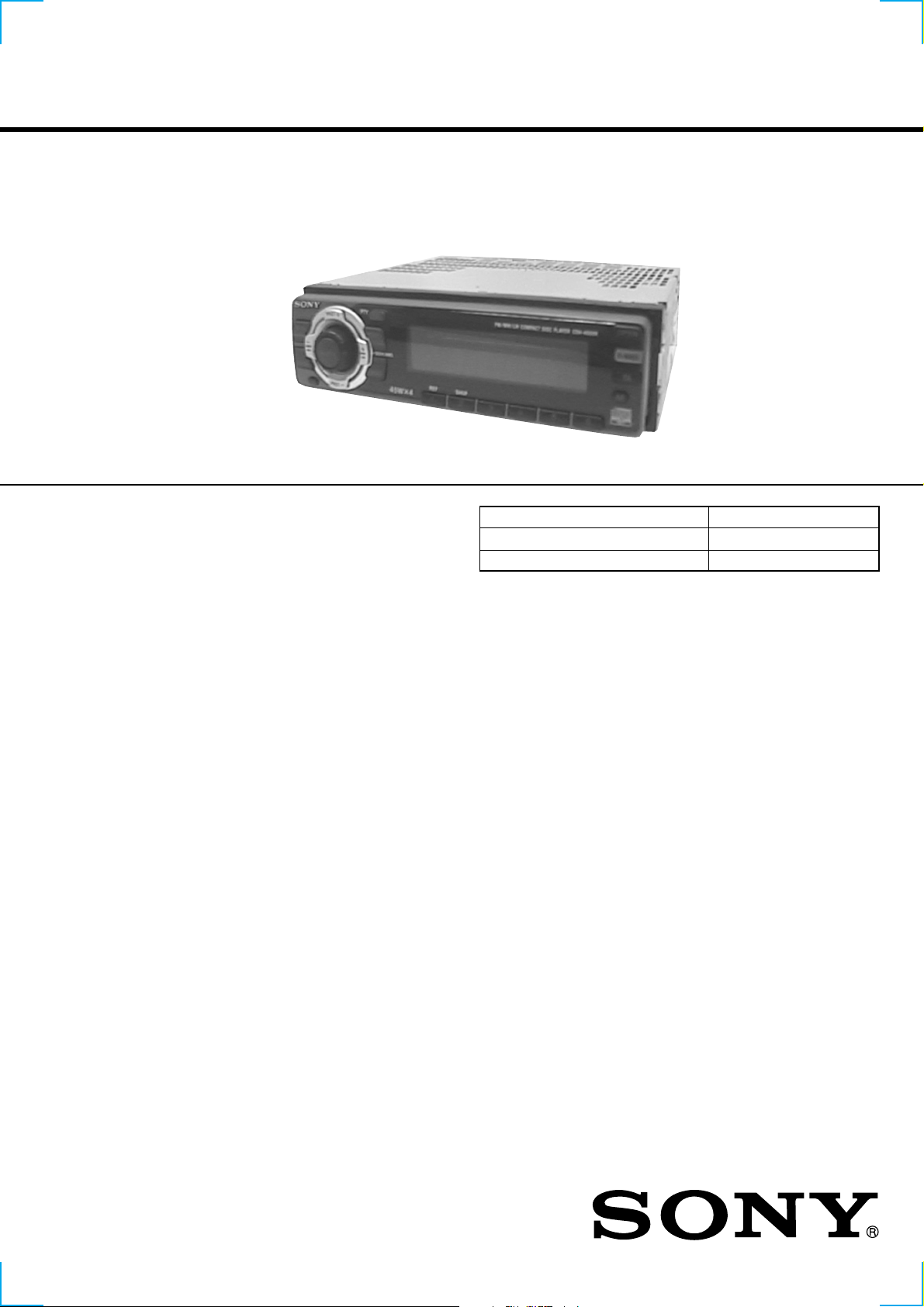
CDX-4000RV
SERVICE MANUAL
Ver 1.1 2000. 08
• The tuner and CD sections have no adjustments.
SPECIFICATIONS
Model Name Using Similar Mechanism CDX-3900R/4000R/4000RX
CD Drive Mechanism Type MG-383Z-121//Q
Optical Pick-up Name KSS-720A
AEP Model
UK Model
CD player section
Signal-to-noise ratio 90 dB
Frequency response 10 – 20,000 Hz
Wow and flutter Below measurable limit
Tuner section
FM
Tuning range 87.5 – 108.0 MHz
Aerial terminal External aerial connector
Intermediate frequency 10.7 MHz/450 kHz
Usable sensitivity 8 dBf
Selectivity 75 dB at 400 kHz
Signal-to-noise ratio 66 dB (stereo),
72 dB (mono)
Harmonic distortion at 1 kHz
0.6% (stereo),
0.3% (mono)
Separation 35 dB at 1 kHz
Frequency response 30 – 15,000 Hz
MW/LW
Tuning range MW: 531 – 1,602 kHz
LW: 153 – 279 kHz
Aerial terminal External aerial connector
Intermediate frequency 10.7 MHz/450 kHz
Sensitivity MW: 30 µV
LW: 40 µV
Power amplifier section
Outputs Speaker outputs
(sure seal connectors)
Speaker impedance 4 – 8 ohms
Maximum power output 50 W × 4 (at 4 ohms)
General
Outputs Audio outputs
Power aerial relay control
lead
Power amplifier control
lead
Telephone ATT control
lead
Tone controls Bass ±9 dB at 100 Hz
Treble ±9 dB at 10 kHz
Power requirements 12 V DC car battery
(negative ground)
Dimensions Approx. 178 × 50 × 183 mm
(w/h/d)
Mounting dimension Approx. 182 × 53 × 162 mm
(w/h/d)
Mass Approx. 1.2 kg
Supplied accessories Parts for installation and
connections (1 set)
Front panel case (1)
Design and specifications are subject to change without
notice.
FM/MW/LW COMPACT DISC PLAYER
1
Ver 1.1 2000. 08
SERVICE NOTES
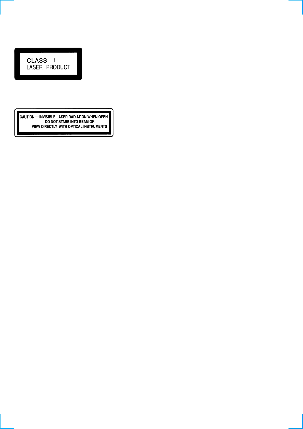
This product is classified as a CLASS 1 LASER PRODUCT.
This label is located on the bottom of the
chassis.
This label is located on the drive unit's internal
chassis.
When replacing the chassis (T) of mechanism deck which have
the “CAUTION LABEL” attached, please be sure to put a new
CAUTION LABEL (3-223-913-11) to the chassis (T).
NOTES ON HANDLING THE OPTICAL PICK-UP BLOCK
OR BASE UNIT
The laser diode in the optical pick-up block may suffer electrostatic
breakdown because of the potential difference generated by the
charged electrostatic load, etc. on clothing and the human body.
During repair, pay attention to electrostatic breakdown and also use
the procedure in the printed matter which is included in the repair
parts.
The flexible board is easily damaged and should be handled with
care.
NOTES ON LASER DIODE EMISSION CHECK
The laser beam on this model is concentrated so as to be focused on
the disc reflective surface by the objective lens in the optical pickup block. Therefore, when checking the laser diode emission, observe from more than 30 cm away from the objective lens.
TABLE OF CONTENTS
1. GENERAL
Location of controls................................................................. 3
Getting Started......................................................................... 3
Setting the clock ...................................................................... 3
CD Player ................................................................................ 3
Radio ....................................................................................... 4
RDS ......................................................................................... 4
Other Functions ....................................................................... 6
Additional Information............................................................ 7
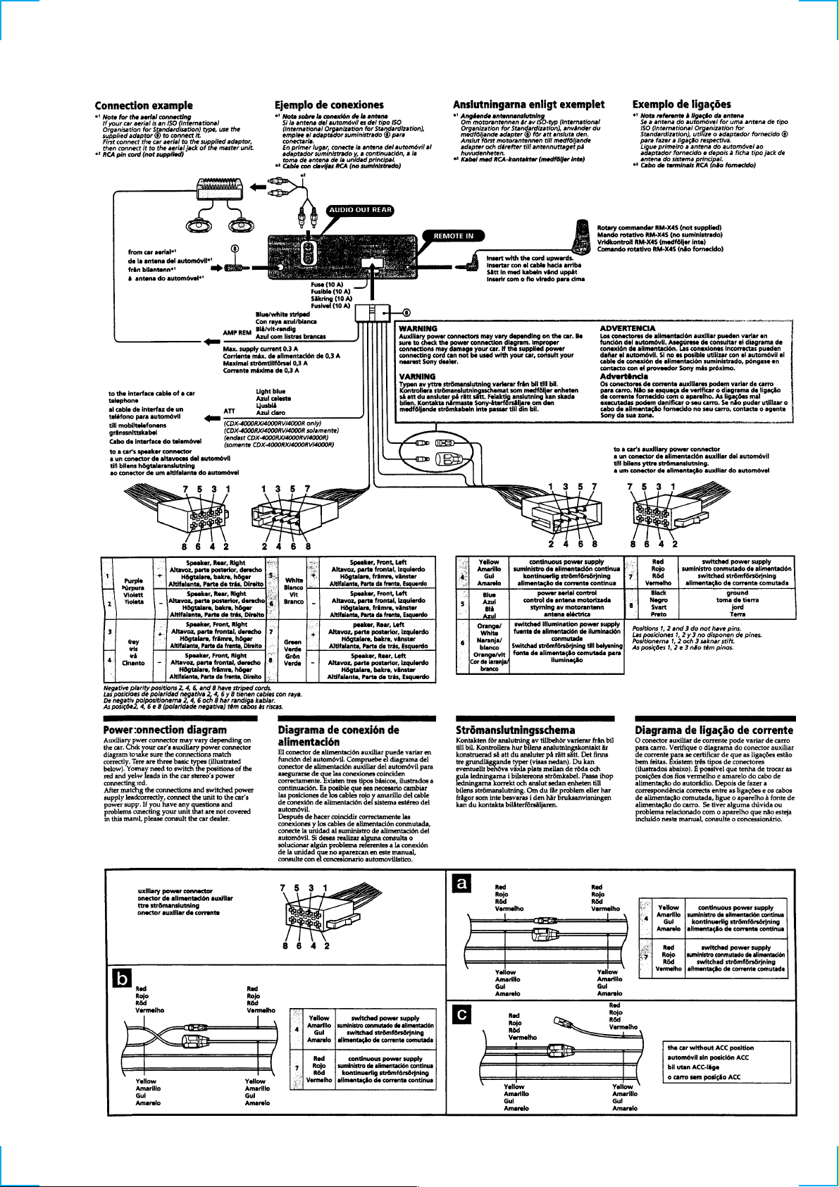
Connections ............................................................................. 8
2. DISASSEMBLY
2-1. Sub Panel Assy.................................................................. 10
2-2. CD Mechanism Block ....................................................... 10
2-3. Main Board ....................................................................... 11
2-4. Heat Sink ...........................................................................11
2-5. Chassis (T) Assy................................................................12
2-6. Lever Assy .........................................................................12
2-7. Servo Board....................................................................... 13
2-8. ARM Roller Assy .............................................................. 13
2-9. Chassis (OP) Assy............................................................. 14
2-10. Optical Pick-up Block ....................................................... 14
3. DIAGRAMS
3-1. IC Pin Descriptions ........................................................... 15
3-2. Block Diagram –CD Section–........................................... 21
3-3. Block Diagram –Tuner Section–....................................... 22
3-4. Block Diagram –Display Section–.................................... 23
3-5. Circuit Boards Location .................................................... 23
3-6. Printed Wiring Boards –CD Mechanism Section–............ 24
3-7. Schematic Diagram –CD Mechanism Section (1/2)– ....... 26
3-8. Schematic Diagram –CD Mechanism Section (2/2)– ....... 27
3-9. Printed Wiring Board –Main Section– .............................. 28
3-10. Schematic Diagram –Main Section (1/3)– ........................30
3-11. Schematic Diagram –Main Section (2/3)– ........................31
3-12. Schematic Diagram –Main Section (3/3)– ........................32
3-13. Schematic Diagram –Sub (CD) Section–.......................... 33
3-14. Printed Wiring Board –Sub (CD) Section– ....................... 34
3-15. Printed Wiring Board –Key Section– ................................35
3-16. Schematic Diagram –Key Section–...................................36
Notes on Chip Component Replacement
• Never reuse a disconnected chip component.
• Notice that the minus side of a tantalum capacitor may be dam-
aged by heat.
SAFETY-RELATED COMPONENT WARNING!!
COMPONENTS IDENTIFIED BY MARK 0 OR DOTTED LINE
WITH MARK 0 ON THE SCHEMATIC DIAGRAMS AND IN
THE PARTS LIST ARE CRITICAL TO SAFE OPERATION.
REPLACE THESE COMPONENTS WITH SONY PARTS WHOSE
P ART NUMBERS APPEAR AS SHOWN IN THIS MANU AL OR
IN SUPPLEMENTS PUBLISHED BY SONY.
2
4. EXPLODED VIEWS
4-1. Chassis Section ................................................................. 40
4-2. Front Panel Section ........................................................... 41
4-3. CD Mechanism Section (1) ...............................................42
4-4. CD Mechanism Section (2) ...............................................43
4-5. CD Mechanism Section (3) ...............................................44
5. ELECTRICAL PARTS LIST ........................................ 45
SECTION 1
GENERAL
This section is extracted
from instruction manual.
3
45678910
SECTION 2
DISASSEMBLY
Note : Follow the disassembly procedure in the numerical order given.
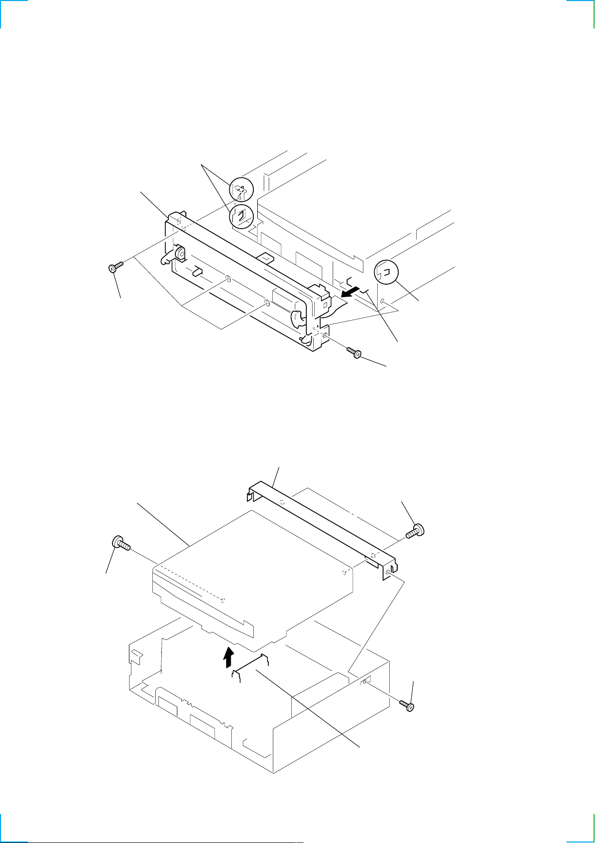
2-1. SUB PANEL ASSY
4 two claws
6 sub panel assy
2 PTT 2.6x8
2-2. CD MECHANISM BLOCK
5 CD mechanism block
2 PTT 2.6x6
3 claw
5 CN500
1 PTT 2.6x8
7 bracket (CD)
6 PTT 2.6x5
3
1 PTT 2.6x5
4 CN301
8
8
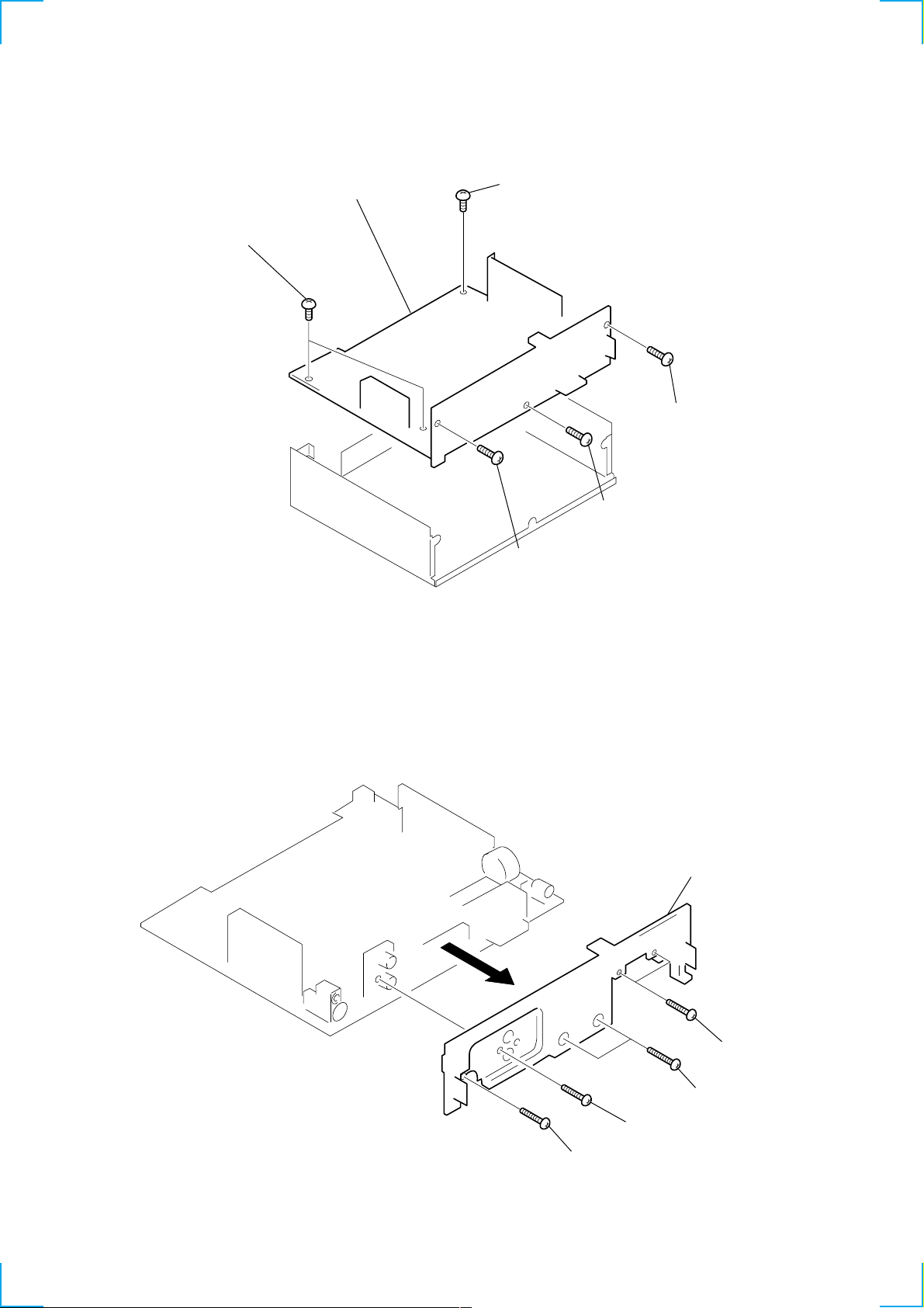
2-3. MAIN BOARD
6 MAIN board
5 ground point screws
(PTT 2.6x6)
4 ground point screws
(PTT 2.6x6)
3 PTT 2.6x
2 PTT 2.6x8
1 PTT 2.6x8
2-4. HEAT SINK
5 heat sink
4 PTT 2.6x
3 PTT 2.6x12
1 PTT 2.6x8
2 PTT 2.6x8
11
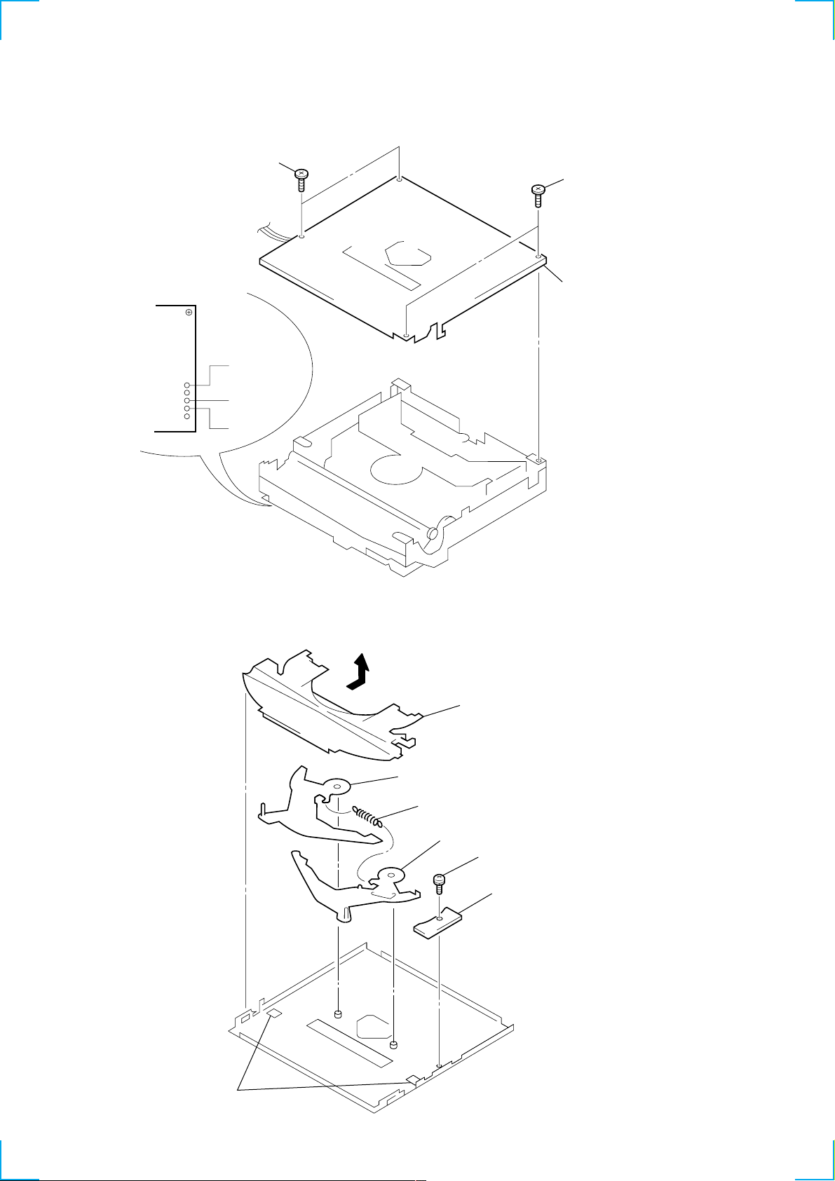
2-5. CHASSIS (T) ASSY
2 P 2x3
3 P 2x3
2-6. LEVER ASSY
1 Unsolder the
lead wires.
4 chassis (T) assy
black
red
white
4 claws
5 guide (disc)
6 lever (R) assy
3 tension spring (LR)
7 lever (L) assy
1 PS 2x4
2 DISC IN SW board
12
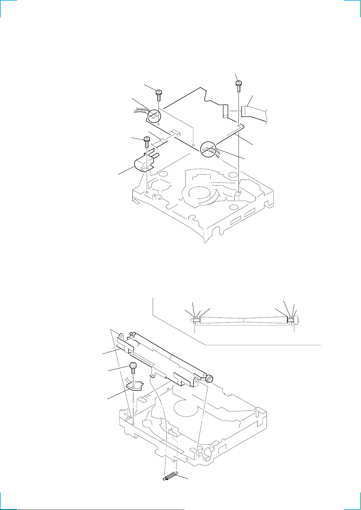
2-7. SERVO BOARD
7 PS 2x4
8 PS 2x4
3 Removal the solders.
1 CN3
5 P 2x3
6 loading motor assy
2 CN2
9 SERVO board
4 Removal the solders.
2-8. ARM ROLLER ASSY
• When installing, take note of the positions
arm (roller) and washers. (Fig. 1)
2 arm roller assy
3 PS 2x3
4 LOAD SW board
shaft retainer
washer (RA)
arm
washer
Fig. 1
washer
arm
shaft retainer
washer (RA)
1 tension spring (RA)
13
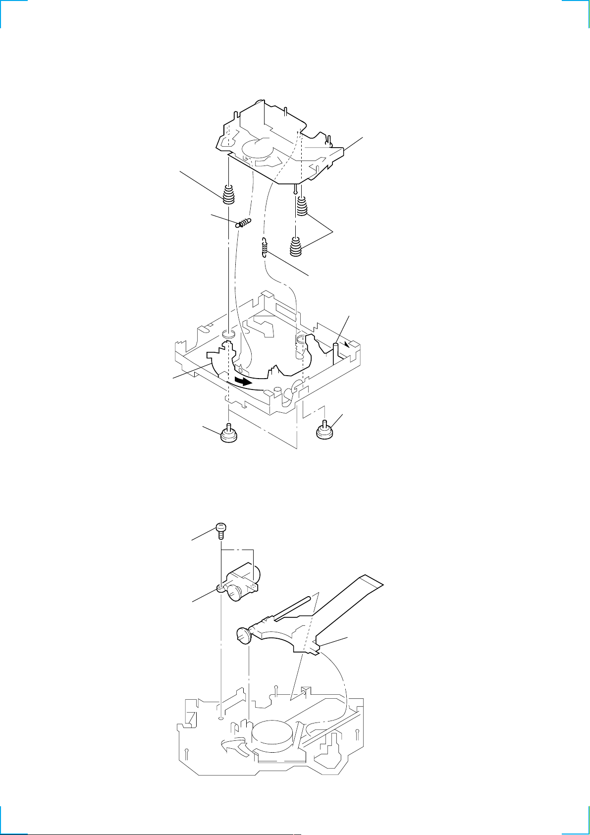
2-9. CHASSIS (OP) ASSY
8 compression spring (FL)
1 tension spring (KF1)
7 chassis (OP) assy
9 compression spring (FL)
2 tension spring (KR1)
5 Fit lever (D) in the
direction of the arrow.
6 Turn loading ring in the
direction of the arrow.
4 damper (T)
2-10. OPTICAL PICK-UP BLOCK
1 P 2x3
2 sled motor assy
3 damper (T)
3 optical pick-up block
14

SECTION 3
DIAGRAMS
3-1. IC PIN DESCRIPTIONS
• IC501 CXD2598Q (DIGITAL SERVO, DIGITAL SIGNAL PROCESSOR) (SERVO BOARD)
Pin No. Pin Name I/O Pin Description
1 DVDD — Digital power supply pin
2 DVSS — Digital ground
3 SOUT O Servo brock serial data output (Not used.)
4 SOCK O Servo brock serial data read clock output (Not used.)
5 XOLT O Servo brock serial data latch output (Not used.)
6 SQSO O Sub Q 80 bit, PCM peak and level data output. CD TEXT data output
7 SQCK I Clock input from SQSO read output.
8 SCSY I Fixed at “L”.
9 SBSO O Serial output of sub-P to W. (Not used.)
10 EXCK I Clock input from SBSO read output. (Fixed at “L”)
11 XRST I System reset (“L”: Reset)
12 STSM I System mute input (Fixed at “L”)
13 DATA I Serial data input from CPU.
14 XLAT I Latch input from CPU. Latch serial data at the falling edge.
15 CLOK I Serial data transfer clock input from CPU.
16 SENS O SENS output for CPU.
17 SCLK I Clock input from SENS serial data read.
18 ATSK I/O Input/output for anti-shock.
19 WFCK O WFCK (Write Flame Clock) output (Not used.)
20 XUGF O XUGF output (Not used.)
21 XPCK O XPCK output (Not used.)
22 GFS O GFS output
23 C2PO O C2PO output (Not used.)
24 SCOR O “H” output at either detection, sub code sync S0 or S1.
25 C4M O 4.2336 MHz output (Not used.)
26 WDCK O Word clock input f=2Fs (Not used.)
27 COUT I/O Track number count signal input/output (Not used.)
28 MIRR I/O Mirror signal input/output (Not used.)
29 DVSS — Digital ground
30 DVDD — Digital power supply pin
31 DFCT I/O Diffect signal input/output (Not used.)
32 FOK I/O Focus OK signal output
33 PWM1 I External control input of spindle motor.
34 LOCK I/O Lock signal input/output
35 MDP O Servo control output of spindle motor.
36 SSTP I Disc most inner track detection signal input
37 FSTIO I/O 2/3 frequency division output of pins ih and ij. (Not used.)
38 SFDR O Sled drive output
39 SRDR O Sled drive output
40 TFDR O Tracking drive output
41 TRDR O Tracking drive output
42 FFDR O Focus drive output
43 FRDR O Focus drive output
44 DVDD — Digital power supply pin
45 DVSS — Digital ground
46 TEST I Test pin (Fixed at “L”)
47 TES1 I Test pin (Fixed at “L”)
48 XTSL I X’tal select input (“L”: 16.9344 MHz, “H”: 33.8688 MHz)
49 VC I Center voltage input
50 FE I Focus error signal input
51 SE I Sled error signal input
15
Pin No. Pin Name I/O Pin Description
52 TE I Tracking error signal input
53 CE I Center servo analog input
54 RFDC I RF signal input
55 ADIO O Test pin (Not used.)
56 AVSSO — Analog ground
57 IGEN I Constant current input from OP amplifier.
58 AVDDO — Analog ground
59 ASYO O EFM full-swing output (“L”: VSS, “H”: VDD)
60 ASYI I Asymmetry comparate voltage input
61 RFAC I EFM signal input
62 AVSS3 — Analog ground
63 CLTV I VCO control voltage input from master.
64 FILO O Filter output for master PLL (slave=digital PLL)
65 FILI I Filter input from master PLL.
66 PCO O Charge pump output for master PLL.
67 AVDD3 — Analog power supply pin
68 BIAS I Asymmetry circuit constant current input
69 VCTL I VCO2 control input from wideband EFM PLL. (Not used.)
70 V16M O VCO2 oscillator output for wideband EFM PLL. (Not used.)
71 VPCO O Charge pump output for wideband EFM PLL. (Not used.)
72 DVSS — Digital ground
73 MD2 I Digital out ON/OFF control input (“L”: OFF, “H”: ON)
74 DOUT O Digital out output
75 ASYE I Asymmetry circuit ON/OFF input (“L”: OFF, “H”: ON)
76 DVDD — Digital power supply pin
77 LRCK O D/A interface LR clock output (f=Fs)
78 LRCKI I D/A interface LR clock input
79 PCMD O D/A interface serial data output (2’s COMP, MSB fast)
80 PCMD I D/A interface serial data input (2’s COMP, MSB fast)
81 BCK O D/A interface bit clock output
82 BCKI I D/A interface bit clock input
83 EMPH O Emphasis ON/OFF signal output
84 EMPHI I Emphasis ON/OFF signal input (“H”: ON, “L”: OFF)
85 XVDD — Power supply for master clock.
86 XTAI I X’tal oscillator input from master clock (16.9344 MHz).
87 XTAO O X’tal oscillator output for master clock (16.9344 MHz).
88 XVSS — Ground pin for master clock.
89 AVDD1 — Analog power supply pin
90 AOUT1 O Lch analog output
91 AIN1 I Lch OPAMP input
92 LOUT1 O Lch LINE output
93 AVSS1 — Analog ground
94 AVSS2 — Analog ground
95 LOUT2 O Rch LINE output
96 AIN2 I Rch OPAMP input
97 AOUT2 O Rch analog output
98 AVDD2 — Analog power supply pin
99 RMUT O Rch “0” detect Flug (Not used.)
100 LMUT O Lch “0” detect Flug (Not used.)
16
 Loading...