

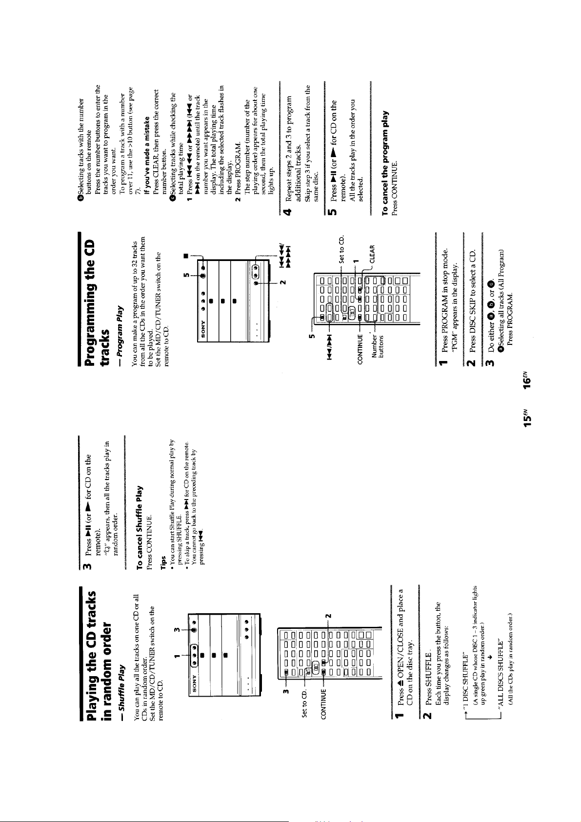
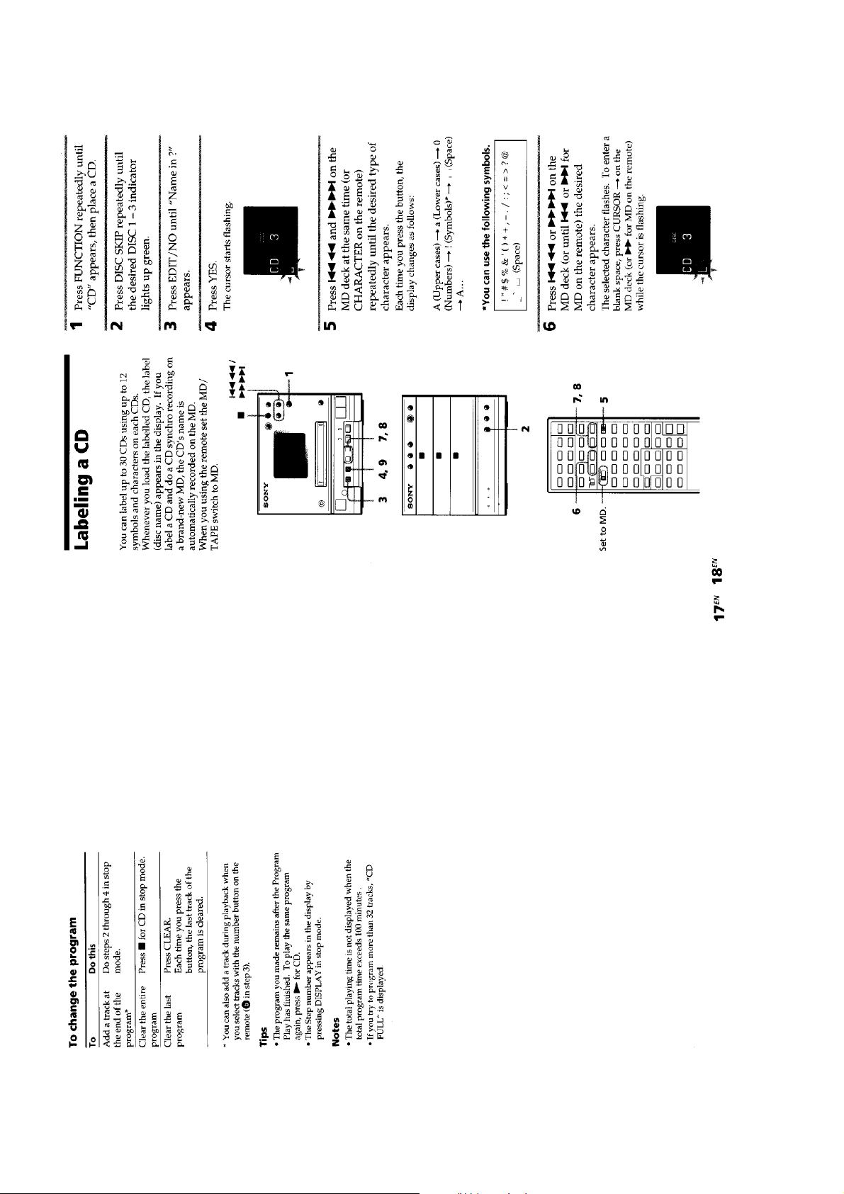
Page 1
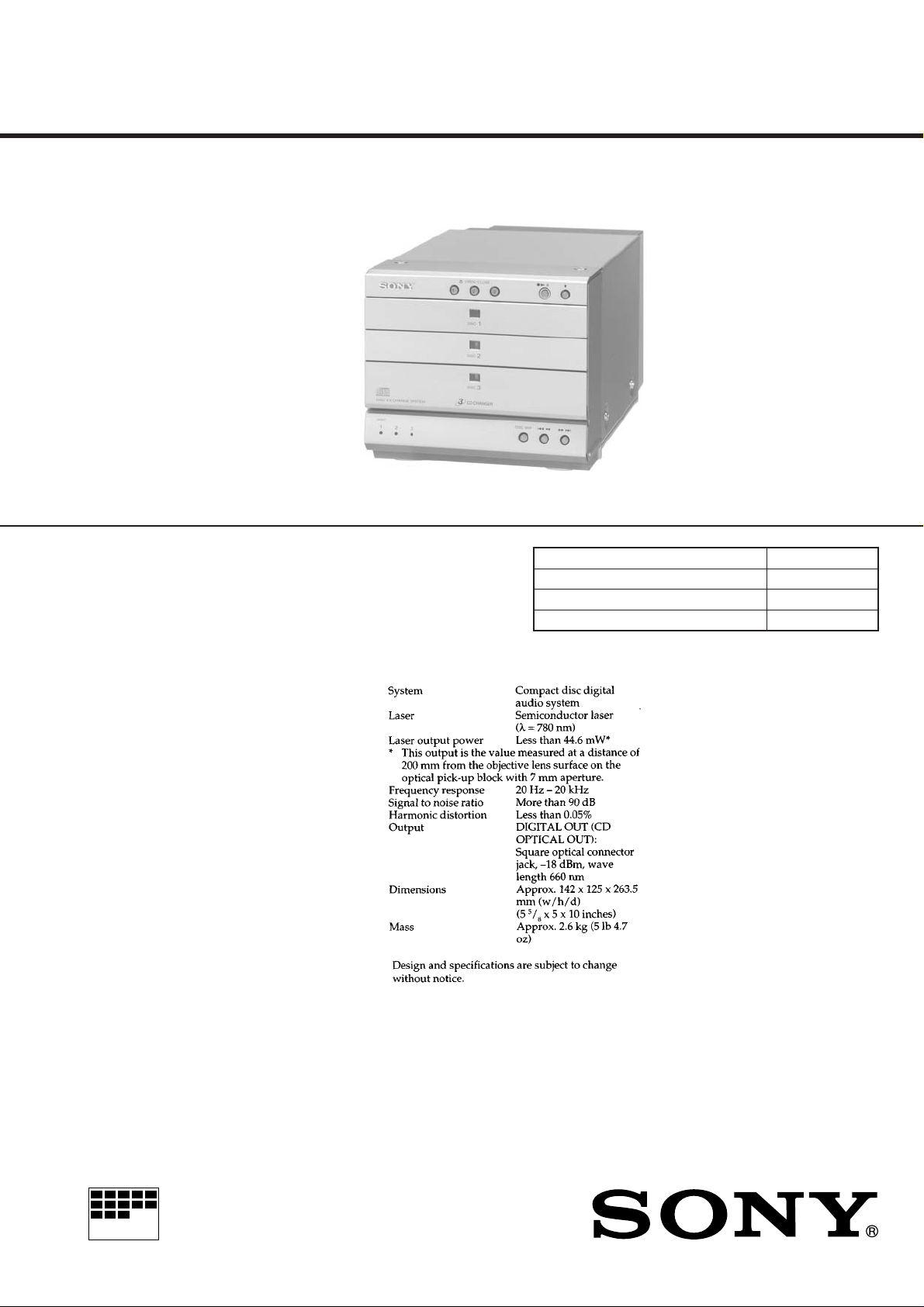
CDP-M11C
SERVICE MANUAL
CDP-M11C is the CD section
in CMT-M11C.
US Model
Canadian Model
AEP Model
UK Model
E Model
Model Name Using Similar Mechanism NEW
CD Mechanism Type CDM42-5BD19
Base Unit Name BU-5BD19
Optical Pick-up Name KSS-213BA/S1NP
SPECIFICATIONS
MICROFILM
COMPACT DISC PLAYER
Page 2
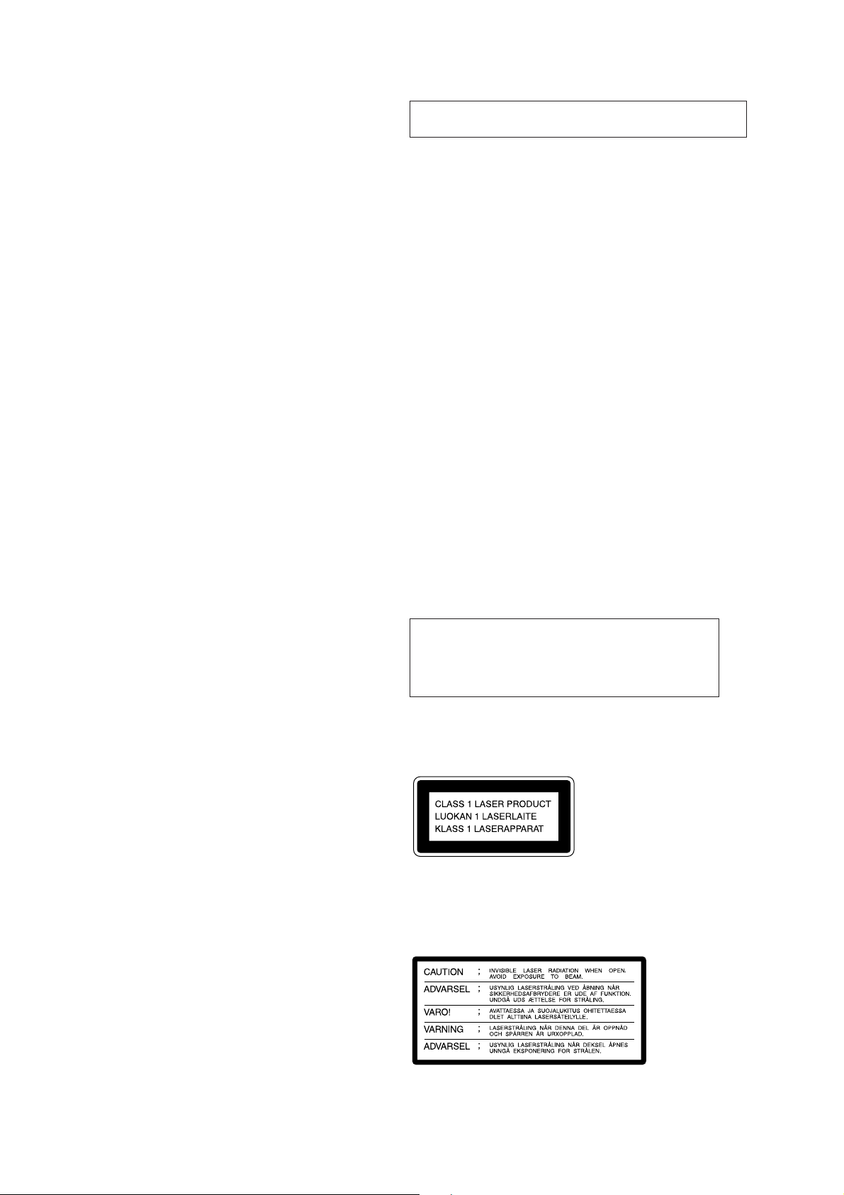
TABLE OF CONTENTS
1. SERVICING NOTES
1-1. Mechanism Motor Direct Drive Mode ............................ 3
1-2. Aging Mode..................................................................... 3
2. GENERAL ................................................................... 4
3. DISASSEMBLY.......................................................... 8
4. TEST MODE..............................................................12
NOTES ON HANDLING THE OPTICAL PICK-UP
BLOCK OR BASE UNIT
The laser diode in the optical pick-up block may suffer electrostatic break-down because of the potential difference generated
by the charged electrostatic load, etc. on clothing and the human
body.
During repair, pay attention to electrostatic break-down and also
use the procedure in the printed matter which is included in the
repair parts.
The flexible board is easily damaged and should be handled with
care.
5. ELECTRICAL ADJUSTMENTS ......................... 12
6. DIAGRAMS
6-1. Printed Wiring Board – BD Section – ............................. 15
6-2. Schematic Diagram – BD Section –................................17
6-3. Schematic Diagram
– MAIN/PANEL/MOTOR Section – .............................. 21
6-4. Printed Wiring Boards
– MAIN/PANEL/MOTOR Section – .............................. 25
6-5. IC Pin Function Description............................................ 32
7. EXPLODED VIEWS ................................................ 34
8. ELECTRICAL PARTS LIST................................39
NOTES ON LASER DIODE EMISSION CHECK
The laser beam on this model is concentrated so as to be focused
on the disc reflective surface by the objective lens in the optical
pick-up block. Therefore, when checking the laser diode emission, observe from more than 30 cm away from the objectiv e lens.
Notes on chip component replacement
• Never reuse a disconnected chip component.
• Notice that the minus side of a tantalum capacitor may be dam-
aged by heat.
Flexible Circuit Board Repairing
• Keep the temperature of the soldering iron around 270 ˚C dur-
ing repairing.
• Do not touch the soldering iron on the same conductor of the
circuit board (within 3 times).
• Be careful not to apply force on the conductor when soldering
or unsoldering.
CAUTION
Use of controls or adjustments or performance of
procedures other than those specified herein may
result in hazardous radiation exposure.
SAFETY-RELATED COMPONENT WARNING!!
COMPONENTS IDENTIFIED BY MARK ! OR DOTTED LINE
WITH MARK ! ON THE SCHEMATIC DIAGRAMS AND IN
THE PARTS LIST ARE CRITICAL TO SAFE OPERATION.
REPLACE THESE COMPONENTS WITH SONY PARTS WHOSE
PART NUMBERS APPEAR AS SHOWN IN THIS MANUAL
OR IN SUPPLEMENTS PUBLISHED BY SONY.
ATTENTION AU COMPOSANT AYANT RAPPORT
À LA SÉCURITÉ!
LES COMPOSANTS IDENTIFIÉS P AR UNE MARQUE ! SUR
LES DIAGRAMMES SCHÉMATIQUES ET LA LISTE DES
PIÈCES SONT CRITIQUES POUR LA SÉCURITÉ DE
FONCTIONNEMENT. NE REMPLACER CES COM- POSANTS
QUE P AR DES PIÈCES SONY DONT LES NUMÉROS SONT
DONNÉS DANS CE MANUEL OU D ANS LES SUPPLÉMENTS
PUBLIÉS PAR SONY.
This appliance is classified as a CLASS 1 LASER product.
The CLASS 1 LASER PRODUCT MARKING is located on
the rear exterior.
Laser component in this product is capable of emitting radiation
exceeding the limit for Class 1.
The following caution label is located inside the unit.
– 2 –
Page 3
SECTION 1
SERVICING NOTES
1-1. MECHANISM MOTOR DIRECT DRIVE MODE
• Functional Overview
A mechanism has three motors (M400, M401 and M402), and
if a motor does not run, each motor can be driven during the
time that the button is pressed.
• Setting Method
While pressing DISC SKIP button and 6 OPEN/CLOSE 3
button, insert the AC plug cord into the AC outlet. (Disc LEDs
are all blinking in green and orange.)
• Button Input and Operation in Mechanism Motor Direct
Drive Mode
Table 1-1.
BUTTON OPERATION MOTOR
) + Carrier UP
= 0 Carrier DOWN
^ Tray IN
p Tray OUT
6 OPEN/
CLOSE 1
6 OPEN/
CLOSE 2
Gear
Chucking
M400
M402
M401
• Releasing Method
Turn off the power switch, and this mode is reset.
1-2. AGING MODE
For the AGING MODE, refer to the CMT-M11C service manual
(Parts No.: 9-960-794-11).
– 3 –
Page 4
This section is extracted
from instruction manual.
SECTION 2
GENERAL
– 4 –
Page 5
– 5 –
Page 6
– 6 –
Page 7
– 7 –
Page 8
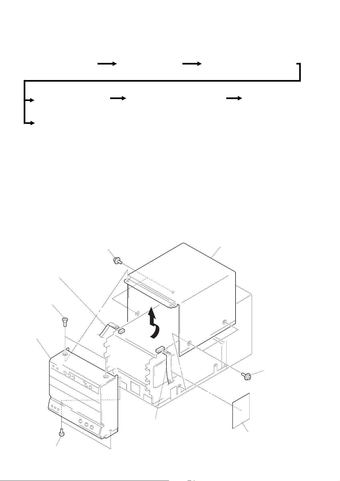
• This set can be disassembled in the order shown below.
SECTION 3
DISASSEMBLY
COVER, FRONT PANEL SECTION
(Page 8)
POWER/TRAY ADDRESS BOARD
(Page 10)
OPTICAL PICK-UP (KSS-213BA/S1NP)
(Page 11)
Note: Follow the disassembly procedure in the numerical order given.
BACK COVER, MAIN BOARD
(Page 9)
DISC TABLE ASS’Y, MOTOR DRIVE BOARD
(Page 10)
COVER, FRONT PANEL SECTION
REINFORCEMENT (TOP), CARRIER ASS’Y
(Page 9)
FRAME (L), (R) ASS’Y
(Page 11)
5
wire (flat type) (5 core)
(CN109)
2
two screws
(ALUMINUM)
7
front panel section
1
two screws
(CASE 3 TP2)
3
cover
1
two screws
(CASE 3 TP2)
6
two screws
(+BTT M 3
5
wire (flat type) (7 core)
(CN110)
×
6)
4
cushion (T-SW)
– 8 –
Page 9
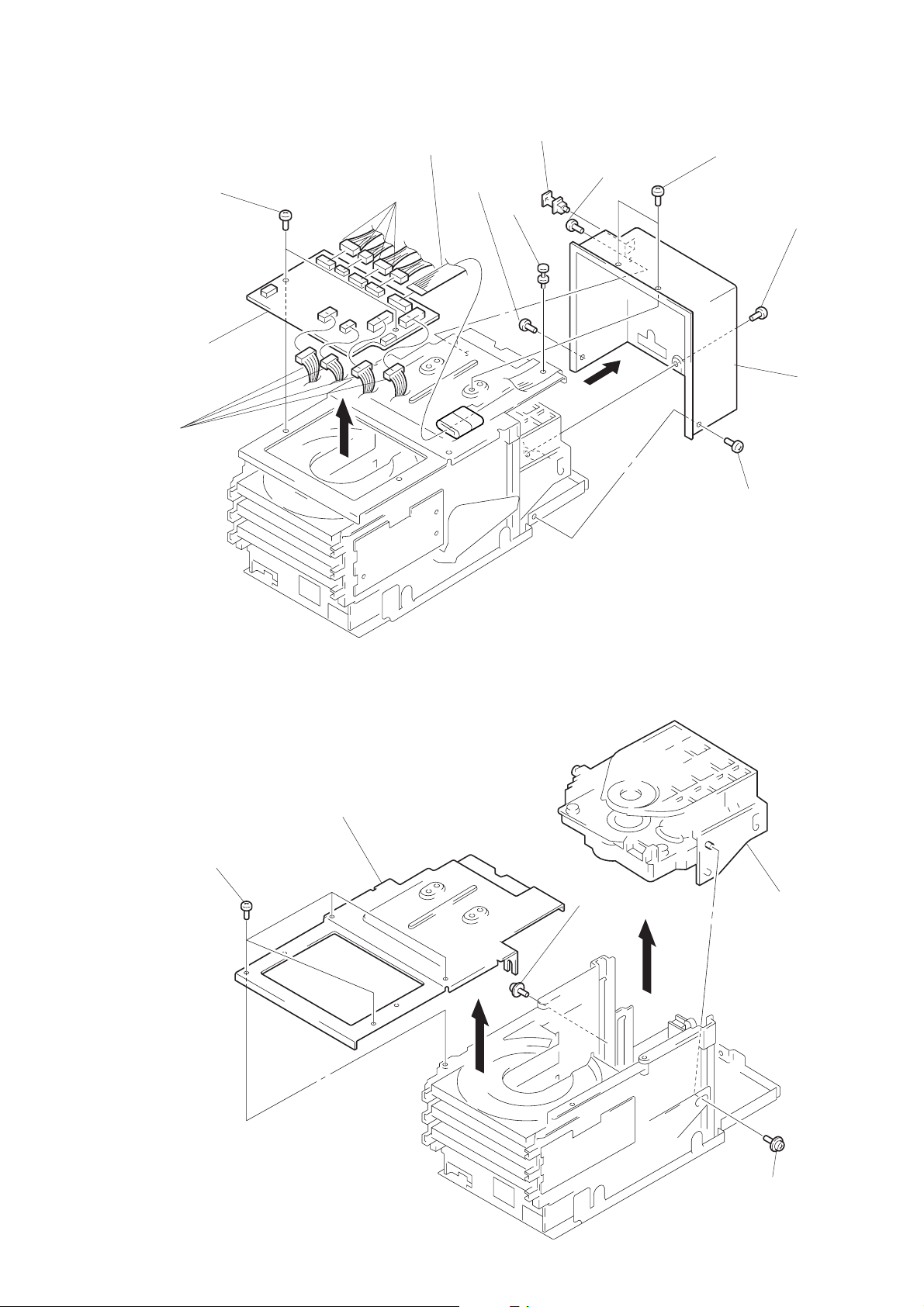
BACK COVER, MAIN BOARD
8
two screws
(+BVTT3
9
main board
6
four connectors
(CN105 - 108)
×
6)
6
four connectors
(CN100 - 103)
7
FPC cable
(CN104)
3
screw
(+BTTM3
5
1
supplied with OPT cap
2
×
6)
rivet
screw
(+BVTP3
×
10)
3
two screws
(+BTTM3
3
screw
(+BTTM3
×
6)
3
screw
(+BTTM3
4
back cover
×
6)
×
6)
REINFORCEMENT (TOP), CARRIER ASS’Y
2
reinforcement (TOP)
1
four screws
(+BV3
×
8)
3
screw
(+PTPWH2.6
4
×
8)
carrier ass’y
– 9 –
3
screw
(+PTPWH2.6
×
8)
Page 10
POWER/TRAY ADDRESS BOARD
3
power board
2
two screws
(+P3
×
5)
1
screw
(+BVTP3
7
sheet (F)
4
5
rivet
×
8)
sheet (S)
9
four washers
8
tray address board
DISC TABLE ASS’Y, MOTOR DRIVE BAORD
5
Remove the four solders of
mode motor ass’y (M401),
motor (O/C) ass’y (M402).
7
three connectors
(CN203, 405, 406)
2
screw
3
two screws
(+P3
(+BVTT3
×
4)
×
5)
8
motor dirve board
7
two connectors
(CN201, 202)
6
screw
(+BVTT 3
6
three screws
(+P2.6
×
8)
×
5)
1
three disc table ass’y
4
joint (front)
– 10 –
2
screw
(+BVTT3
×
5)
Page 11
FRAME (L), (R) ASS’Y
lever (up and down L)
2
screw
(BVTT3
×
5)
A
6
frame (L), (R) ass’y
B
3
screw
(P3
×
4)
4
joint (middle)
lever (up and down R)
2
screw
(BVTT3
×
5)
Rotate the worm gear in direction
1
to lower the levers (up and down L, R)
in direction
B
.
A
OPTICAL PICK-UP (KSS-213BA/S1NP)
7
optical pick-up
(KSS-213BA/S1NP)
3
two screws
4
Lift up this base
(outsart) assy.
(PTPWH M2.6
×
6)
5
four screws
(BV3
×
8)
Note: when mounting the frame (L) and
(R) assemblies, engage the elevating shaft withe the grooves of racks
(up and down).
2
carrier ass’y
8
wire (flat type) (16 core)
3
two screws
(PTPWH M2.6
×
6)
6
sled shaft
5
Open the lever to direction
of the arrow
A
.
A
– 11 –
1
yoke bracket
Page 12

SECTION 4
+
–
BD board
TP (RF)
TP (VC)
oscilloscope
(AC range)
TEST MODE
SECTION 5
ELECTRICAL ADJUSTMENTS
BD TEST MODE
• Functional Overview
The BD test mode is used to check the BD block. When this
mode is activated, a mechanism is kept in stop status and GFS
is not monitored.
A checking status is displayed with disc LEDs.
• Setting the Test Mode
1. Load a disc on the tray of disc 1 and have a disc chucked.
2. Turn off the power switch once, and connect TP (TEST) and
TP (GND) on MAIN board, then again turn on the power
switch.
3. Thus, the test mode is activated.
Note:When the test mode is activated, disc LEDs are all turned
off and GFS is not monitored.
• Button Input and Operation in Test Mode
Table 4-1.
BUTTON
6 OPEN/
CLOSE 1
6 OPEN/
CLOSE 2
6 OPEN/
CLOSE 3
• Releasing the Test Mode
1. Turn off the power switch, and disconnect a short wire between TP (TEST) and TP (GND) on MAIN board.
2. Thus, the set becomes ready for normal operation.
LED on DISC 1 turns on, normal focus
gain is set, and CLV is fixed to 12 cm.
LED on DISC 2 turns on, tracking servo
and sled servo are turned off.
LED on DISC 3 turns on, and tracking
balance value is displayed.
OPERATION
Notes:
1. Use YEDS-18 disc (Par t No.: 3-702-101-01) unless otherwise
indicated.
2. Use the oscilloscope with more than 10 MΩ impedance.
3. Clean an object lens by an applicator with neutral detergent
when the signal level is low than specified value with the following checks.
4. Adjust the focus bias adjustment when optical pick-up is replaced.
Focus Bias Adjustment
This adjustment is to be done when the optical pick-up is replaced.
Condition: This adjustment is performed with the set placed hori-
zontally.
Connection:
Adjustment Procedure:
1. Connect the oscilloscope to TP (RF) and TP (VC) on BD board.
2. Turned power switch on. (Stop mode)
3. Put disc (YEDS-18) in and press the ^ button.
4. Adjust RV101 so that the oscilloscope waveform is as shown
in the figure below (eye pattern).
A good eye pattern means that the diamond shape (≈) in the
center of the waveform can be clearly distinguished.
• RF signal reference waveform (eye pattern)
VOLT/DIV: 200 mV
TIME/DIV: 150 ns
(with the 10 : 1 probe
in use)
1.3 ± 0.3 Vp-p
When observing the eye pattern, set the oscilloscope for AC
range and raise vertical sensitivity.
S-Curve Check
Connection:
oscilloscope
BD board
TP (FEO)
TP (VC)
Procedure:
1. Connect the oscilloscope to TP (FEO) and TP (VC) on BD
board.
2. Connect the TP (FOK) and TP (GND) with lead wire.
3. Turned power switch on.
4. Put disc (YEDS-18) in and turned power switch on again and
actuate the focus search. (actuate the focus search when disc
table is moving in and out.)
+
–
– 12 –
Page 13

5. Confirm that the oscilloscope waveform (S-curve) is symmetrical between A and B. And confirm peak to peak level within
2.4 ± 0.7 Vp-p.
S-curve waveform
6. After check, remove the lead wire connected in step 2.
Note: • Try to measure several times to make sure that the ratio
of A : B or B : A is more than 10 : 7.
• Take sweep time as long as possible and light up the
brightness to obtain best waveform.
RF Level Check
Connection:
BD board
TP (RF)
TP (VC)
Procedure:
1. Connect the oscilloscope to TP (RF) and TP (VC) on BD board.
2. Turned power switch on. (stop mode)
3. Put disc (YEDS-18) in and press the ^ button.
4. Confirm that oscilloscope waveform is clear and check RF
signal level is correct or not.
Note: Clear RF signal waveform means that the shape “≈” can
be clearly distinguished at the center of the waveform.
RF signal waveform
symmetry
A
B
oscilloscope
+
–
level: 1.3 ± 0.3 Vp-p
within 2.4 ± 0.7 Vp-p
VOLT/DIV: 200 mV
TIME/DIV: 500 ns
(with the 10 : 1 probe
in use)
Traverse waveform
A
B
level: 300 ± 100 mVp-p
7. After check, remove the lead wire connected in step 1.
Focus/Tracking Gain Adjustment (RV102, RV103)
This gain has a margin, so even if it is slightly off. There is no
problem.
Therefore, do not perform, this adjustment.
Please note that it should be fixed to mechanical center position
when you moved and do not know original position.
Adjustment Location :
[BD BOARD] – Side B –
IC102
FOK
RF
RV101
IC101
TEI
FEO
FEI
RV102
TEO
RV103
VC
GND
IC104
[MAIN BOARD] – Component Side –
SECTION 6
DIAGRAMS
• Circuit Boards Location
LIGHT CONNECTOR board
MAIN board
PANEL (UPPER) board
POWER board
TRAY ADDRESS board
PANEL (LOWER) board
CHUCKING SW board
BD board
GEAR SELECT board
E-F Balance (Traverse) Check
Connection:
oscilloscope
BD board
TP (TEO)
TP (VC)
Procedure:
1. Connect the TP (TEST) and TP (GND) with lead wire. (Test
mode)
2. Connect the oscilloscope to TP (TEO) and TP (VC) on BD
board.
3. Turned power switch on.
4. Put disc (YEDS-18) in and press the ^ button.
5. Press the 6 OPEN/CLOSE 2 button. (Tracking servo and
sled servo are turned off.)
6. Confirm that the oscilloscope waveform is symmetrical on the
top and bottom in relation to 0 Vdc, and check this level.
(DC range)
+
–
– 13 –
IC103
TP
(GND)TP(TEST)
MOTOR DRIVE board
PHOTO SENSOR board
– 14 –
Page 14

Page 15

Page 16

• Waveforms
3 Vp-p
10 MHz
– BD Section –
1 IC101 #¡ (RFO) (PLAY Mode)
500 mV/DIV, 500 ns/DIV 6 IC103 @∞ (XPCK)
– MAIN/PANEL/MOTOR Section –
1 IC103 $™ (X1)
2 IC101 $¢ (TEI) (PLAY Mode)
50 mV/DIV, 1 µs/DIV
3 IC101 2 (FEI) (PLAY Mode)
50 mV/DIV, 1 µs/DIV
Approx. 1.3 Vp-p
Approx. 100 mVp-p
Approx. 150 mVp-p
5.3 Vp-p
14 ns
7 IC103 @™ (BCLK)
5 Vp-p
474 ns
8 IC103 @º (LRCK)
5.1 Vp-p
4 IC103 3 (MDP) (PLAY Mode)
7.6 µs
5 IC103 @• (RFCK)
136 µs
22.7 µs
9 IC104 6 (XTO)
2.6 Vp-p
4.6 Vp-p
16.9344 MHz
5.1 Vp-p
– 20 –
Page 17

Page 18

Page 19

• IC Block Diagrams
– BD Section –
IC101 CXA1782BQ
PHD2
PHD1
36
35 34
PHD
–
+
–
+
APC
–
+
RF IV AMP1
LD
33
RF M
32
–
+
–
+
LEVELS
+
–
FOK
RF O
31
–
+
–
+
MIRR
RF I
30
–
+
+
–
+
–
29CP28
CB
DFCT
CC126CC225FOK
27
–
+
24 SENS
IIL
+
–
TTL
23 C. OUT
–
+
RF IV AMP2
37FE BIAS
+
–
38F
39E
40EI
BAL1
41VEE
42TEO
TOG1
43LPFI
44TEI
45ATSC
46TZC
47TDFCT
48VC
–
+
F IV AMP
–
+
E IV AMP
BAL2
BAL3
TOG2
TOG3
• WINDOW COMP
ATSC
–
+
FE AMP
TE AMP
+
–
DFCT
TTL
IIL
FZC COMP
TZC COMP
DFCT
FS4
–
+
–
+
–
+
• IIL DATA RESISTOR • INPUT SHIFT RESISTOR
TOG1-3 FS1-4 TG1-2 TM1-7 PS1-4
BAL1-3
–
–
+
+
HPF COMP LPF COMP
+
–
• FCS PHASE
COMPENSATION
TM1
FS2
+
–
• ADDRESS DECODER
• OUTPUT DECODER
• TRACKING
• PHASE
COMPENSATION
TG1
FS1
• ISET
TM6
TM5
TM4
TM3
TM7
TG2
• F SET
TTL
TM2
22 XRST
21 DATA
20 XLT
IIL
19 CLK
18 VCC
17 ISET
–
16 SL 0
+
15 SL M
14 SL P
+
1312TA O
–
11
TGU
10
TG2
FSET
TA M
3
2
1
FEI
FEO
FDFCT
4
FLB
FGD
FE O
FE M
SRCH
9
8
7
6
5
– 29 –
Page 20

IC102 BA6397FP
A
DRIVE
BUFFER
GND
28
DRIVE
BUFFER
1
OUT1A
OUT4
27
BUFFER
2
OUT1B
LEVEL
DRIVE
THERMAL
SHIFT
OUT4BIN4A
26
25
DRIVE
BUFFER
SHIFT
LEVEL
SHUT DOWN
3
4
IN1A
IN1B
IN4B
24
5
TR-B
CC
VC
V
22
23
V
REGULATOR
7
6
XRST
REG 0
VCCIN3B
21
CC
V
CC
20
DRIVE
BUFFER
IN3A
OUT3BOUT3AOP+
19
18
SHIFT
LEVEL
17
DRIVE
BUFFER
OP–
15
16
DRIVER MUTE
SHIFT
LEVEL
8
GND
9
IN2A
DRIVE
BUFFER
10
IN2B
11
OUT2A
12
OUT2B
DRIVE
BUFFER
13
GND
14
OP-OUT
IC103 CXD2507AQ
1
FOK
2
MON
MDP
3
4
MDS
5
LOCK
6
TEST
7
FILO
8
FILI
9
PCO
10
VSS
11
AVSS
12
CLTV
13
AVDD
14
RF
15
BIAS
16
ASYI
17
ASYO
18
ASYE
19
WDCK
SERVO AUTO
SEQUENCER
14
INTERFACE
DIGITAL
PLL
ASYMMETRY
CORRECTOR
5
XLON
CPU
LRCK
SPOD
PCMD
RAM
BCLK
SPOC
SPOB
SPOA
5
DEMODULATOR
16K
XUGF
GTOP
DD
CLKO
V
SUB CODE
PROCESSOR
EFM
3
ERROR
CORRECTOR
3
DD
V
XPCK
XLTO
DATO
CNIN
4
D/A
INTERFACE
GFS
RFCK
CZPO
SEIN
DIGITAL
CLV
6
XROF
CLOK
52535455565758596061626364
32313029282726252423222120
MNT3
XLAT
DIGITAL
MNT1
OUT
CLOCK
GENERATOR
51
DATA
XRST
50
SENS
49
MUTE
48
SQCK
47
SQSO
46
45
EXCK
SBSO
44
SCOR
43
42
V
SS
WFCK
41
EMPH
40
DOUT
39
C4M
38
37
FSTT
XTSL
36
XTAO
35
XTAI
34
33
MNTO
– 30 –
Page 21

IC104 PCM1710U-B
LRCIN
DIN
BCKIN
CLKO
XTO
DGND
V
VCC2R
GND2R
EXT1R
EXT2R
VOUTR
GND1
1
2
3
4
5
XTI
6
7
8
DD
9
10
11
12
13
14
INPUT
INTERFACE DIGITAL
TIMING
CONTROL
5-LEVEL DAC
RIGHT
LOW-PASS FILTER
RIGHT
3-STAGE AMP
RIGHT
FILTER
NOISE
SHAPER
MODE
CONTROL
5-LEVEL DAC
LEFT
LOW-PASS FILTER
LEFT
3-STAGE AMP
LEFT
28
27
26
25
24
23
22
21
20
19
18
17
16
15
ML/DSD
MC/DM2
MD/DM1
MUTE
MODE
CKSL
DGND
DD
V
VCC2L
GND2L
EXT1L
EXT2L
VOUTL
V
CC
1
– MAIN/PANEL/MOTOR Section –
IC101 CXA1291P
+VIN2
–VIN2
–VIN3
OUT2
AMP2
AMP3
11
OUT3
78
10 1615
9
+VIN3
VEEVEE
AMP1
THERMAL SHUT
CURRENT LIMITER
14
OUT1
DOWN AND
NC
236
–VIN1
NC
+VIN1
1
VCC
– 31 –
Page 22

6-5. IC PIN FUNCTION DESCRIPTION
• MAIN BOARD IC103 µPD78014FGC-532-AB8 (SYSTEM CONTROLLER)
Pin No. Pin Name I /O Function
1 C.SW2 I Detection input from the chucking address switch (S402)
2 C.SW1 I Detection input from the chucking address switch (S401)
3 G.SW2 I Detection input from the gear select switch (S404)
4 G.SW1 I Detection input from the gear select switch (S403)
5 B.SENS I Detection input from the BD vertical position sensor (PH400)
6 B.SW I Detection input from the BD bottom switch (S400)
7 T3.SW3 I Detection input from the disc 3 tray horizontal address switch (S433)
8 T3.SW2 I Detection input from the disc 3 tray horizontal address switch (S432)
9 VSS — Ground terminal
10 T3.SW1 I Detection input from the disc 3 tray horizontal address switch (S431)
11 T2.SW3 I Detection input from the disc 2 tray horizontal address switch (S423)
12 T2.SW2 I Detection input from the disc 2 tray horizontal address switch (S422)
13 T2.SW1 I Detection input from the disc 2 tray horizontal address switch (S421)
14 T1.SW3 I Detection input from the disc 1 tray horizontal address switch (S413)
15 T1.SW2 I Detection input from the disc 1 tray horizontal address switch (S412)
16 T1.SW1 I Detection input from the disc 1 tray horizontal address switch (S411)
17 BDTEST I Setting terminal for BD test mode “L”: test mode, Normally: “H”
18 LED0 O Drive signal output for the disc 3 pointer LED (D600; green) “L”: LED on
19 LED1 O Drive signal output for the disc 1 pointer LED (D602; orange) “L”: LED on
20 LED2 O Drive signal output for the disc 3 pointer LED (D600; orange) “L”: LED on
21 LED3 O Drive signal output for the disc 1 pointer LED (D602; green) “L”: LED on
22 LED4 O Drive signal output for the disc 2 pointer LED (D601; green) “L”: LED on
23 LED5 O Drive signal output for the disc 2 pointer LED (D601; orange) “L”: LED on
24 VSS — Ground terminal
25 LED6 O Drive signal output for the PAUSE LED (D620; orange) “L”: LED on
26 LED7 O Drive signal output for the PLAY LED (D620; green) “L”: LED on
27 QB-DATA0 I/O
28 QB-DATA1 I/O
29 QB-DATA2 I/O
30 QB-DATA3 I/O
31 BDUP O
32 BDDOWN O
33 GEAR O
34 CHUCK O
35 RESET I
36 QB-CLK I
MECHA-POWER
37
38 QB-READY I/O
39 SCOR I Sub-code sync (S0+S1) detection signal input from the CXD2507AQ (IC103)
40 VDD — Power supply terminal (+5V)
Two-way data bus with the master controller on HMD-M11 (mini-disc deck/tuner/preamp
system)
BD block up/down motor drive signal output to the CXA1291P (IC101) *1
Chucking/gear motor drive signal output to the CXA1291P (IC101)
System reset signal input from the reset signal generator (IC303) “L”: reset
For several hundreds msec. after the power supply rises, “L” is output, then it changes to “H”
Data transfer clock signal input from the master controller on HMD-M11 (mini-disc deck/tuner/
preamp system)
O Power supply on/off control signal output of the CXA1291P (IC101) “H”: power on
Ready signal in/out terminal with the master controller on HMD-M11 (mini-disc deck/tuner/
preamp system)
– 32 –
Page 23

Pin No. Pin Name I /O Function
41 X2 O Main system clock output terminal (10 MHz)
42 X1 I Main system clock input terminal (10 MHz)
43 IC (VSS) — Not used (fixed at “L”)
44 XT2 O Sub system clock output terminal Not used (fixed at “L”)
45 XT1 I Sub system clock input terminal Not used (fixed at “L”)
46 AVSS — Ground terminal (for A/D converter)
47 KEY0 I
48 KEY1 I
49 FSW O
50 SENS I Internal status (SENSE) signal input from the CXD2507AQ (IC103)
51 DFLAT O Serial data latch pulse output to the PCM1710U (IC104)
52 BDPWR O Power supply on/off control signal output of the BD block “H”: power on
53 LOADOUT O
54 LOADIN O
55 AVDD — Power supply terminal (+5V) (for A/D converter)
56 AVREF I Reference voltage input terminal (+5V) (for A/D converter)
57 SUBQ I Sub-code Q data signal input from the CXD2507AQ (IC103)
58 NC O Not used (open)
59 SQCLK O Sub-code Q data reading clock signal output to the CXD2507AQ (IC103)
60 XRST O Reset signal output for the BD block “L”: reset
61 XLAT O Serial data latch pulse output to the CXD2507AQ (IC103)
62 NC I Not used (fixed at “L”)
63 DATA O Serial data output to the CXD2507AQ (IC103) and PCM1710U (IC104)
64 CLK O Serial data transfer clock signal output to the CXD2507AQ (IC103) and PCM1710U (IC104)
Key input terminal (A/D input) ) + , = 0 , DISC SKIP keys (S601 to S603)
Key input terminal (A/D input) 6 OPEN/CLOSE 1 to 3, ^ , p keys (S621 to S625)
Focus gain selection signal output to the CXA1782BQ (IC101)
“H”: normal mode, “L”: focus gain down mode
Loading motor drive signal output to the CXA1291P (IC101) *2
*1 BD block up/down motor control
Operation
Terminal
BDUP (pin #¡) “L” “H” “L”
BDDOWN (pin #™) “L” “L” “H”
*2 Loading motor control
Operation
Terminal
LOADOUT (pin %£) “L” “H” “L”
LOADIN (pin %¢) “L” “L” “H”
OFF UP DOWN
OFF OUT IN
– 33 –
Page 24

SECTION 7
EXPLODED VIEWS
NOTE:
• -XX and -X mean standardized parts, so they
may have some difference from the original
one.
• Color Indication of Appearrance Parts
Example:
KNOB, BALANCE (WHITE) . . . (RED)
↑↑
Parts Color Cabinet's Color
(1) COVER, FRONT PANEL SECTION
7
8
6
9
5
4
3
• Items marked “*” are not stocked since they
are seldom required for routine service. Some
delay should be anticipated when ordering
these items.
• The mechanical parts with no reference num-
ber in the exploded views are not supplied.
• Hardware (# mark) list is given in the last of
the electrical parts list.
13
12
11
10
17
16
15
The components identified by mark
! or dotted line with mark ! are
critical for safety.
Replace only with part number
specified.
Les composants identifiés par une
marque ! sont critiquens pour la
sécurité.
Ne les remplacer que par une pièce
portant le neméro spécifié.
14
23
14
13
14
18
2
22
21
20
1
#1
19
Ref. No. Part No. Description Remark Ref. No. Part No. Description Remark
1 4-986-512-01 PANEL (AL-CD), FRONT
2 4-942-636-21 EMBLEM (NO.3.5), SONY
3 4-975-365-01 SCREW (ALUMINUM)
4 4-986-523-01 INDICATOR (PLAY)
5 4-986-528-01 SPRING (B)
13 3-363-099-51 SCREW (CASE 3 TP2)
14 4-951-620-31 SCREW (2.6), +BVTP
* 15 1-663-505-11 PANEL (LOWER) BOARD
* 16 1-663-504-11 PANEL (UPPER) BOARD
17 4-986-521-01 BUTTON (PLAY)
6 X-4947-768-1 DOOR (D3) ASSY
7 X-4947-767-1 DOOR (D2) ASSY
8 X-4947-766-1 DOOR (D1) ASSY
9 4-986-527-01 SPRING (A)
10 4-986-513-01 PANEL (MOLD CD), FRONT
11 4-986-520-01 BUTTON (EJECT)
12 1-777-814-11 WIRE (FLAT TYPE) (5 CORE)
18 1-777-813-11 WIRE (FLAT TYPE) (9 CORE)
19 4-986-522-01 BUTTON (EDIT)
20 4-986-564-01 CUSHION (FOOT)
21 4-986-524-01 INDICATOR (DISC)
* 22 4-986-531-01 BRACKET (C), GROUND
* 23 4-975-358-91 COVER
– 34 –
Page 25

(2) MAIN SECTION
53
US, Canadian
not supplied
55
59
supplied with IC300
#1
not supplied
52
#2
51
#3
54
#3
#2
#1
#12
56
#1
#1
#4
57
55
not supplied
51
not supplied
#5
58
60
Ref. No. Part No. Description Remark Ref. No. Part No. Description Remark
51 4-933-134-51 SCREW (+PTPWH 2.6X8)
* 52 A-4699-662-A MAIN BOARD, COMPLETE (US, Canadian)
* 52 A-4699-664-A MAIN BOARD, COMPLETE (EXCEPT US,
53 4-988-654-01 CUSHION (F)
* 54 1-663-502-11 LIGHT CONNECTOR BOARD
55 3-531-576-11 RIVET
not supplied
Canadian)
* 56 4-986-532-11 COVER, BACK (US, Canadian, AEP, UK)
* 56 4-986-532-23 COVER, BACK (E, Hong Kong, Singapore,
Malaysia)
* 57 1-663-503-11 POWER BOARD
* 58 1-663-507-11 TRAY ADDRESS BOARD
59 1-500-418-11 CORE (US, Canadian)
60 4-990-188-01 WASHER
– 35 –
Page 26

(3) FRAME (L), (R) ASS’Y SECTION
(CDM42-5BD19)
not supplied
103
101
104
105
104
105
104
105
not
supplied
102
#7
107
106
107
106
107
106
#8
not supplied
#6
not supplied
#7
#9
108
110
111
110
109
not
supplied
114
112
110
113
111
110
109
#8
#9
116
not supplied
#8
#7
not supplied
#7
not supplied
not supplied
#2
Ref. No. Part No. Description Remark Ref. No. Part No. Description Remark
101 X-4947-734-1 TRAIN ASSY, GEAR
* 102 1-663-509-11 GEAR SELECT BOARD
103 4-933-134-51 SCREW (+PTPWH 2.6X8)
104 4-986-652-01 SPRING, COMPRESSION
105 4-986-321-01 GEAR
106 4-986-650-01 SLEEVE (ON/OFF)
107 3-533-073-01 WASHER
* 108 1-663-508-11 CHUCKING SW BOARD
109 4-986-319-01 GEAR (TRAY DRIVING)
110 3-669-595-00 WASHER (2), STOPPER
111 4-986-320-01 PULLEY (TRAY DRIVING)
112 3-359-466-01 BELT (FR), SQUARE
113 4-986-653-01 SPRING (CLICK), LEAF
* 114 X-4947-732-1 CHASSIS (TRAY DRIVING) ASSY, SUB
115 3-696-510-01 WASHER (3), STOPPER
116 X-4947-834-1 TABLE ASSY, DISC
115
#8
115
– 36 –
Page 27

(4) CHASSIS SECTION
(CDM42-5BD19)
157
159
156
#6
155
not
supplied
160
158
159
154
not supplied
161
159
not
supplied
153
152
M401
174
not supplied
not supplied
#6
157
#6
173
M402
#10
164
162
163
159
165
166
171
M400
#6
159
153
152
159
168
not supplied
159
167
169
#6
not
supplied
#6
#7
151
Ref. No. Part No. Description Remark
* 151 X-4947-730-1 CHASSIS ASSY
152 4-986-335-01 GEAR (MODE B)
153 4-986-336-01 GEAR (MODE A)
154 4-986-334-01 GEAR (SELECT), CAM
* 155 X-4947-731-1 BRACKET (LOADING PULLEY) ASSY
156 4-986-324-01 GEAR (SHAFT DECELERATION)
157 3-669-595-00 WASHER (2), STOPPER
158 4-986-325-01 PULLEY (LOADING)
159 3-558-708-21 WASHER, STOPPER
160 3-319-030-01 BELT
161 3-359-412-01 GEAR (REEL MOTOR)
162 4-986-312-01 GEAR, WORM
163 3-359-466-01 BELT (FR), SQUARE
164 4-986-311-01 WHEEL, WORM
170
172
not supplied
Ref. No. Part No. Description Remark
165 4-986-310-01 GEAR (RACK DRIVING)
166 4-986-347-01 GEAR (MODE C)
* 167 4-986-309-01 RACK (UP AND DOWN)
168 4-986-345-01 GEAR (CHUCKING), CAM
169 3-831-441-XX CUSHION (B), CABINET
* 170 1-663-506-11 MOTOR DRIVE BOARD
* 171 1-663-510-11 PHOTO SENSOR BOARD
172 4-965-822-01 FOOT
173 3-317-552-61 SCREW (M1.7X2.0)
174 3-343-251-01 SCREW (M2.6X2.5)
M400 A-4672-209-A MOTOR (CARRIER U/D) ASSY (BD UP/DOWN)
M401 A-4672-211-A MOTOR ASSY, MODE (CHUCKING/GEAR)
M402 A-4672-210-A MOTOR (O/C) ASSY (LOADING)
– 37 –
Page 28

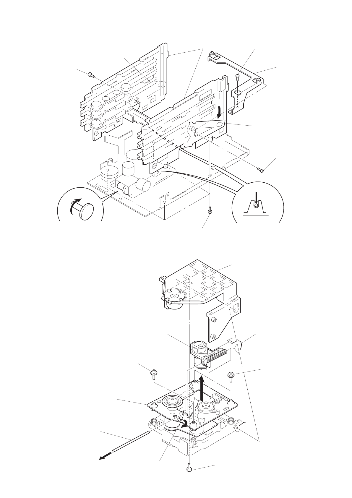
(5) CARRIER ASS’Y, OPTICAL PICK-UP SECTION
(BU-5BD19)
207
203
202
206
208
205
209
M101
204
#11
M102
216
220
208
206
210
217
215
211
not supplied
212
214
213
201
#9
not supplied
Ref. No. Part No. Description Remark
* 201 4-986-348-01 PLATE (BU HOLDER), LOCK
* 202 X-4947-735-1 HOLDER ASSY, BU
203 4-982-447-01 SPRING (BU), COMPRESSION
204 4-951-620-01 SCREW (2.6X8), +BVTP
* 205 A-4673-402-A BD BOARD, COMPLETE
206 4-951-940-01 INSULATOR (BU)
207 4-917-565-01 SHAFT, SLED
208 4-933-134-01 SCREW (+PTPWH M2.6X6)
! 209 8-848-387-01 OPTICAL PICK-UP KSS-213BA/S1NP
210 1-769-069-11 WIRE (FLAT TYPE) (16 CORE)
218
219
The components identified by
mark ! or dotted line with
mark ! are critical for safety.
Replace only with part number
specified.
Ref. No. Part No. Description Remark
* 212 X-4947-833-1 CARRIER ASSY
* 213 4-917-583-21 BRACKET, YOKE
214 4-986-341-01 SLIDER (CHUCKING CAM)
215 3-696-510-01 WASHER (3), STOPPER
216 1-777-631-11 FPC CABLE
217 4-917-564-01 GEAR (P), FLATNESS
218 3-531-576-11 RIVET
219 4-951-620-31 SCREW (2.6), +BVTP
220 4-917-567-01 GEAR (M)
M101 X-4917-523-4 BASE (OUTSART) ASSY (SPINDLE)
Les composants identifiés par une
marque ! sont critiques pour la
sécurité.
Ne les remplacer que par une pièce
portant le neméro spécifié.
211 1-452-864-11 MAGNET (ASSY)
M102 X-4917-504-1 MOTOR ASSY (SLED)
– 38 –
Page 29

SECTION 8
ELECTRICAL PARTS LIST
BD
NOTE:
• Due to standardization, replacements in the
parts list may be different from the parts specified in the diagrams or the components used on
the set.
• -XX and -X mean standardized parts, so they
may have some difference from the original one.
• RESISTORS
All resistors are in ohms.
MET AL: Metal-film resistor.
METAL OXIDE: Metal oxide-film resistor.
F: nonflammable
• Items marked “*” are not stocked since they
are seldom required for routine service.
Some delay should be anticipated when ordering these items.
Ref. No. Part No. Description Remark
* A-4673-402-A BD BOARD, COMPLETE
*******************
< CAPACITOR >
C101 1-126-607-11 ELECT CHIP 47uF 20% 4V
C102 1-163-275-11 CERAMIC CHIP 0.001uF 5% 50V
C103 1-164-346-11 CERAMIC CHIP 1uF 16V
C105 1-163-038-00 CERAMIC CHIP 0.1uF 25V
C106 1-164-695-11 CERAMIC CHIP 0.0022uF 5% 50V
• SEMICONDUCTORS
In each case, u: µ, for example:
uA. . : µA. . uPA. . : µPA. .
uPB. . : µPB. . uPC. . : µPC. .
uPD. . : µPD. .
• CAPACIT ORS
uF: µF
• COILS
uH: µH
The components identified by mark
! or dotted line with mark ! are
critical for safety.
Replace only with part number
specified.
Les composants identifiés par une
marque ! sont critiquens pour la
sécurité.
Ne les remplacer que par une pièce
portant le neméro spécifié.
When indicating parts by reference
number, please include the board.
Ref. No. Part No. Description Remark
C145 1-135-201-11 TANTALUM CHIP 10uF 20% 4V
C146 1-135-201-11 TANTALUM CHIP 10uF 20% 4V
C147 1-163-275-11 CERAMIC CHIP 0.001uF 5% 50V
C148 1-163-275-11 CERAMIC CHIP 0.001uF 5% 50V
C149 1-164-346-11 CERAMIC CHIP 1uF 16V
C153 1-135-259-11 TANTALUM CHIP 10uF 20% 6.3V
C154 1-163-235-11 CERAMIC CHIP 22PF 5% 50V
< CONNECTOR >
C107 1-164-695-11 CERAMIC CHIP 0.0022uF 5% 50V
C108 1-164-232-11 CERAMIC CHIP 0.01uF 50V
C109 1-164-232-11 CERAMIC CHIP 0.01uF 50V
C110 1-163-989-11 CERAMIC CHIP 0.033uF 10% 25V
C111 1-163-038-00 CERAMIC CHIP 0.1uF 25V
C112 1-163-038-00 CERAMIC CHIP 0.1uF 25V
C113 1-164-695-11 CERAMIC CHIP 0.0022uF 5% 50V
C114 1-164-005-11 CERAMIC CHIP 0.47uF 25V
C115 1-126-607-11 ELECT CHIP 47uF 20% 4V
C116 1-163-016-00 CERAMIC CHIP 0.0039uF 10% 50V
C117 1-164-005-11 CERAMIC CHIP 0.47uF 25V
C118 1-107-823-11 CERAMIC CHIP 0.47uF 10% 16V
C119 1-163-038-00 CERAMIC CHIP 0.1uF 25V
C120 1-135-201-11 TANTALUM CHIP 10uF 20% 4V
C121 1-163-038-00 CERAMIC CHIP 0.1uF 25V
C122 1-164-232-11 CERAMIC CHIP 0.01uF 50V
C123 1-163-038-00 CERAMIC CHIP 0.1uF 25V
C124 1-126-607-11 ELECT CHIP 47uF 20% 4V
C125 1-164-232-11 CERAMIC CHIP 0.01uF 50V
C126 1-163-038-00 CERAMIC CHIP 0.1uF 25V
C127 1-164-695-11 CERAMIC CHIP 0.0022uF 5% 50V
C128 1-163-135-00 CERAMIC CHIP 560PF 5% 50V
C129 1-163-038-00 CERAMIC CHIP 0.1uF 25V
C130 1-164-336-11 CERAMIC CHIP 0.33uF 25V
C131 1-163-038-00 CERAMIC CHIP 0.1uF 25V
CNU101 1-770-014-11 CONNECTOR, FFC/FPC 16P
CNU102 1-770-013-11 CONNECTOR, FFC/FPC 19P
< IC >
IC101 8-752-069-56 IC CXA1782BQ
IC102 8-759-291-06 IC BA6397FP
IC103 8-752-372-94 IC CXD2507AQ
IC104 8-759-185-29 IC PCM1710U-B
< TRANSISTOR >
Q101 8-729-010-08 TRANSISTOR MSB710-R
Q102 8-729-424-08 TRANSISTOR UN2111
Q103 8-729-421-22 TRANSISTOR UN2211
< RESISTOR >
R102 1-216-001-00 METAL CHIP 10 5% 1/10W
R103 1-216-049-00 METAL CHIP 1K 5% 1/10W
R104 1-216-097-00 METAL CHIP 100K 5% 1/10W
R105 1-216-093-00 METAL CHIP 68K 5% 1/10W
R106 1-216-093-00 METAL CHIP 68K 5% 1/10W
R107 1-216-093-00 METAL CHIP 68K 5% 1/10W
R108 1-216-093-00 METAL CHIP 68K 5% 1/10W
R109 1-216-097-00 METAL CHIP 100K 5% 1/10W
R112 1-216-083-00 METAL CHIP 27K 5% 1/10W
R113 1-216-083-00 METAL CHIP 27K 5% 1/10W
C132 1-163-037-11 CERAMIC CHIP 0.022uF 10% 25V
C133 1-163-145-00 CERAMIC CHIP 0.0015uF 5% 50V
C134 1-164-346-11 CERAMIC CHIP 1uF 16V
C135 1-163-251-11 CERAMIC CHIP 100PF 5% 50V
C136 1-164-005-11 CERAMIC CHIP 0.47uF 25V
C137 1-164-232-11 CERAMIC CHIP 0.01uF 50V
C139 1-163-235-11 CERAMIC CHIP 22PF 5% 50V
C140 1-163-235-11 CERAMIC CHIP 22PF 5% 50V
C141 1-163-038-00 CERAMIC CHIP 0.1uF 25V
C142 1-163-038-00 CERAMIC CHIP 0.1uF 25V
R114 1-216-101-00 METAL CHIP 150K 5% 1/10W
R115 1-216-101-00 METAL CHIP 150K 5% 1/10W
R116 1-216-061-00 METAL CHIP 3.3K 5% 1/10W
R117 1-216-069-00 METAL CHIP 6.8K 5% 1/10W
R118 1-216-049-00 METAL CHIP 1K 5% 1/10W
R119 1-216-089-00 METAL CHIP 47K 5% 1/10W
R120 1-216-089-00 METAL CHIP 47K 5% 1/10W
R121 1-216-114-00 METAL CHIP 510K 5% 1/10W
R122 1-216-097-00 METAL CHIP 100K 5% 1/10W
R123 1-216-099-00 METAL CHIP 120K 5% 1/10W
– 39 –
Page 30

BD LIGHT CONNECTOR
GEAR SELECTCHUCKING SW
MAIN
Ref. No. Part No. Description Remark
R124 1-216-091-00 METAL CHIP 56K 5% 1/10W
R125 1-216-069-00 METAL CHIP 6.8K 5% 1/10W
R126 1-216-063-00 METAL CHIP 3.9K 5% 1/10W
R127 1-216-089-00 METAL CHIP 47K 5% 1/10W
R128 1-216-105-00 METAL CHIP 220K 5% 1/10W
R129 1-216-049-00 METAL CHIP 1K 5% 1/10W
R130 1-216-079-00 METAL CHIP 18K 5% 1/10W
R131 1-216-079-00 METAL CHIP 18K 5% 1/10W
R132 1-216-061-00 METAL CHIP 3.3K 5% 1/10W
R133 1-216-061-00 METAL CHIP 3.3K 5% 1/10W
R134 1-216-065-00 METAL CHIP 4.7K 5% 1/10W
R135 1-216-065-00 METAL CHIP 4.7K 5% 1/10W
R136 1-216-073-00 METAL CHIP 10K 5% 1/10W
R137 1-216-065-00 METAL CHIP 4.7K 5% 1/10W
R138 1-216-049-00 METAL CHIP 1K 5% 1/10W
R139 1-216-033-00 METAL CHIP 220 5% 1/10W
R140 1-216-081-00 METAL CHIP 22K 5% 1/10W
R141 1-216-061-00 METAL CHIP 3.3K 5% 1/10W
R142 1-216-061-00 METAL CHIP 3.3K 5% 1/10W
R143 1-216-121-00 METAL CHIP 1M 5% 1/10W
R144 1-216-073-00 METAL CHIP 10K 5% 1/10W
R145 1-216-097-00 METAL CHIP 100K 5% 1/10W
R146 1-216-097-00 METAL CHIP 100K 5% 1/10W
R147 1-216-049-00 METAL CHIP 1K 5% 1/10W
R148 1-216-049-00 METAL CHIP 1K 5% 1/10W
R149 1-216-049-00 METAL CHIP 1K 5% 1/10W
R150 1-216-037-00 METAL CHIP 330 5% 1/10W
R151 1-216-037-00 METAL CHIP 330 5% 1/10W
R152 1-216-037-00 METAL CHIP 330 5% 1/10W
R153 1-216-082-00 METAL CHIP 24K 5% 1/10W
R154 1-216-065-00 METAL CHIP 4.7K 5% 1/10W
R156 1-216-085-00 METAL CHIP 33K 5% 1/10W
R157 1-216-069-00 METAL CHIP 6.8K 5% 1/10W
R158 1-216-001-00 METAL CHIP 10 5% 1/10W
Ref. No. Part No. Description Remark
* 1-663-509-11 GEAR SELECT BOARD
******************
< SWITCH >
S403 1-762-847-11 SWITCH, PUSH (1 KEY) (GEAR SELECT)
S404 1-762-847-11 SWITCH, PUSH (1 KEY) (GEAR SELECT)
************************************************************
* 1-663-502-11 LIGHT CONNECTOR BOARD
**********************
< CAPACITOR >
C300 1-126-964-11 ELECT 10uF 20% 50V
C301 1-164-159-11 CERAMIC 0.1uF 50V
< CONNECTOR >
CN303 1-506-468-11 PIN, CONNECTOR 3P
< IC >
IC300 8-749-921-12 IC GP1F32T (DIGITAL OUT)
************************************************************
* A-4699-662-A MAIN BOARD, COMPLETE (US, Canadian)
* A-4699-664-A MAIN BOARD, COMPLETE
(EXCEPT US, Canadian)
*********************
* 4-870-539-00 PLATE, GROUND
< CAPACITOR >
C100 1-107-725-11 CERAMIC CHIP 0.1uF 10% 16V
C101 1-107-725-11 CERAMIC CHIP 0.1uF 10% 16V
C102 1-164-232-11 CERAMIC CHIP 0.01uF 50V
C103 1-126-204-11 ELECT CHIP 47uF 20% 16V
C110 1-107-725-11 CERAMIC CHIP 0.1uF 10% 16V
< VARIABLE RESISTOR >
RV101 1-223-587-11 RES, ADJ, CARBON 22K
RV102 1-223-587-11 RES, ADJ, CARBON 22K
RV103 1-223-587-11 RES, ADJ, CARBON 22K
< SWITCH >
S101 1-572-085-11 SWITCH, LEAF (LIMIT)
< VIBRATOR >
X101 1-579-280-11 VIBRATOR, CRYSTAL (16.9344 MHz)
************************************************************
* 1-663-508-11 CHUCKING SW BOARD
*******************
< SWITCH >
S401 1-692-193-11 SWITCH, PUSH (1 KEY)
(CHUCKING ADDRESS)
S402 1-692-193-11 SWITCH, PUSH (1 KEY)
(CHUCKING ADDRESS)
************************************************************
C112 1-126-206-11 ELECT CHIP 100uF 20% 6.3V
C113 1-107-725-11 CERAMIC CHIP 0.1uF 10% 16V
C114 1-163-009-11 CERAMIC CHIP 0.001uF 10% 50V
C115 1-163-009-11 CERAMIC CHIP 0.001uF 10% 50V
C116 1-163-037-11 CERAMIC CHIP 0.022uF 10% 25V
C117 1-126-393-11 ELECT 33uF 20% 10V
C118 1-126-393-11 ELECT 33uF 20% 10V
C121 1-124-779-00 ELECT CHIP 10uF 20% 16V
C122 1-113-503-11 CERAMIC CHIP 0.0039uF 5% 25V
C123 1-163-143-00 CERAMIC CHIP 0.0012uF 5% 50V
C124 1-126-204-11 ELECT CHIP 47uF 20% 16V
C125 1-126-395-11 ELECT 22uF 20% 16V
C131 1-107-725-11 CERAMIC CHIP 0.1uF 10% 16V
C132 1-107-725-11 CERAMIC CHIP 0.1uF 10% 16V
C133 1-107-725-11 CERAMIC CHIP 0.1uF 10% 16V
C140 1-163-133-00 CERAMIC CHIP 470PF 5% 50V
C141 1-163-133-00 CERAMIC CHIP 470PF 5% 50V
C142 1-163-251-11 CERAMIC CHIP 100PF 5% 50V
C143 1-163-133-00 CERAMIC CHIP 470PF 5% 50V
C144 1-163-251-11 CERAMIC CHIP 100PF 5% 50V
C145 1-163-133-00 CERAMIC CHIP 470PF 5% 50V
C146 1-163-251-11 CERAMIC CHIP 100PF 5% 50V
C147 1-163-243-11 CERAMIC CHIP 47PF 5% 50V
C148 1-163-243-11 CERAMIC CHIP 47PF 5% 50V
C149 1-163-251-11 CERAMIC CHIP 100PF 5% 50V
– 40 –
Page 31

MAIN
Ref. No. Part No. Description Remark
C151 1-124-779-00 ELECT CHIP 10uF 20% 16V
C152 1-113-503-11 CERAMIC CHIP 0.0039uF 5% 25V
C153 1-163-143-00 CERAMIC CHIP 0.0012uF 5% 50V
C154 1-126-204-11 ELECT CHIP 47uF 20% 16V
C155 1-126-395-11 ELECT 22uF 20% 16V
C170 1-107-725-11 CERAMIC CHIP 0.1uF 10% 16V
C171 1-107-725-11 CERAMIC CHIP 0.1uF 10% 16V
C172 1-126-206-11 ELECT CHIP 100uF 20% 6.3V
C181 1-107-725-11 CERAMIC CHIP 0.1uF 10% 16V
C182 1-107-725-11 CERAMIC CHIP 0.1uF 10% 16V
C190 1-107-725-11 CERAMIC CHIP 0.1uF 10% 16V
C191 1-107-725-11 CERAMIC CHIP 0.1uF 10% 16V
C192 1-107-725-11 CERAMIC CHIP 0.1uF 10% 16V
C193 1-107-725-11 CERAMIC CHIP 0.1uF 10% 16V
C194 1-107-725-11 CERAMIC CHIP 0.1uF 10% 16V
< CONNECTOR >
CN100 1-774-180-11 PIN, CONNECTOR (PC BOARD) 6P
CN101 1-774-297-21 PIN, CONNECTOR (PC BOARD) 7P
CN102 1-774-653-21 PIN, CONNECTOR (PC BOARD) 3P
CN103 1-774-731-21 PIN, CONNECTOR (PC BOARD) 5P
CN104 1-778-718-11 CONNECTOR, FFC/FPC 19P
CN105 1-778-795-21 PIN, CONNECTOR (PC BOARD) 9P
CN106 1-778-768-21 PIN, CONNECTOR (PC BOARD) 8P
CN107 1-770-217-11 PIN, CONNECTOR (PC BOARD) 4P
CN108 1-774-180-11 PIN, CONNECTOR (PC BOARD) 6P
CN109 1-774-739-11 CONNECTOR, FFC/FPC 5P
CN110 1-778-719-11 CONNECTOR, FFC/FPC 9P
< DIODE >
Ref. No. Part No. Description Remark
Q114 8-729-424-08 TRANSISTOR UN2111
Q115 8-729-424-08 TRANSISTOR UN2111
Q116 8-729-424-08 TRANSISTOR UN2111
Q117 8-729-424-08 TRANSISTOR UN2111
Q120 8-729-101-07 TRANSISTOR 2SB798-DL
Q121 8-729-216-22 TRANSISTOR 2SA1162-G
Q122 8-729-421-22 TRANSISTOR UN2211
Q123 8-729-120-28 TRANSISTOR 2SC1623-L5L6
Q124 8-729-120-28 TRANSISTOR 2SC1623-L5L6
Q125 8-729-120-28 TRANSISTOR 2SC1623-L5L6
Q126 8-729-424-08 TRANSISTOR UN2111
Q127 8-729-140-75 TRANSISTOR 2SD999-CLCK
Q128 8-729-120-28 TRANSISTOR 2SC1623-L5L6
< RESISTOR >
R100 1-216-061-00 METAL CHIP 3.3K 5% 1/10W
R101 1-216-061-00 METAL CHIP 3.3K 5% 1/10W
R102 1-216-049-00 METAL CHIP 1K 5% 1/10W
R103 1-216-073-00 METAL CHIP 10K 5% 1/10W
R120 1-216-089-00 METAL CHIP 47K 5% 1/10W
R121 1-216-055-00 METAL CHIP 1.8K 5% 1/10W
R122 1-216-055-00 METAL CHIP 1.8K 5% 1/10W
R123 1-216-097-00 METAL CHIP 100K 5% 1/10W
R150 1-216-089-00 METAL CHIP 47K 5% 1/10W
R151 1-216-055-00 METAL CHIP 1.8K 5% 1/10W
R152 1-216-055-00 METAL CHIP 1.8K 5% 1/10W
R153 1-216-097-00 METAL CHIP 100K 5% 1/10W
R160 1-216-033-00 METAL CHIP 220 5% 1/10W
R161 1-216-073-00 METAL CHIP 10K 5% 1/10W
R162 1-216-054-00 METAL CHIP 1.6K 5% 1/10W
D100 8-719-210-33 DIODE EC10DS2
D101 8-719-210-33 DIODE EC10DS2
D102 8-719-210-33 DIODE EC10DS2
D103 8-719-210-33 DIODE EC10DS2
D104 8-719-976-96 DIODE DTZ4.7C
D120 8-719-016-74 DIODE 1SS352
D121 8-719-016-74 DIODE 1SS352
< IC >
IC100 8-759-636-55 IC M5218AFP
IC103 8-759-458-30 IC uPD78014FGC-532-AB8
< COIL >
L100 1-412-348-41 INDUCTOR 47uH
L131 1-414-386-11 INDUCTOR, FERRITE BEAD
L132 1-414-386-11 INDUCTOR, FERRITE BEAD
L133 1-414-386-11 INDUCTOR, FERRITE BEAD
L134 1-414-386-11 INDUCTOR, FERRITE BEAD
L135 1-414-386-11 INDUCTOR, FERRITE BEAD
L136 1-414-386-11 INDUCTOR, FERRITE BEAD
< TRANSISTOR >
Q100 8-729-421-22 TRANSISTOR UN2211
Q101 8-729-101-07 TRANSISTOR 2SB798-DL
Q110 8-729-424-08 TRANSISTOR UN2111
Q111 8-729-424-08 TRANSISTOR UN2111
Q112 8-729-424-08 TRANSISTOR UN2111
Q113 8-729-424-08 TRANSISTOR UN2111
R163 1-216-054-00 METAL CHIP 1.6K 5% 1/10W
R164 1-216-049-00 METAL CHIP 1K 5% 1/10W
R165 1-216-073-00 METAL CHIP 10K 5% 1/10W
R166 1-216-073-00 METAL CHIP 10K 5% 1/10W
R167 1-216-073-00 METAL CHIP 10K 5% 1/10W
R168 1-216-073-00 METAL CHIP 10K 5% 1/10W
R169 1-216-033-00 METAL CHIP 220 5% 1/10W
R200 1-216-073-00 METAL CHIP 10K 5% 1/10W
R201 1-216-073-00 METAL CHIP 10K 5% 1/10W
R202 1-216-073-00 METAL CHIP 10K 5% 1/10W
R203 1-216-073-00 METAL CHIP 10K 5% 1/10W
R204 1-216-049-00 METAL CHIP 1K 5% 1/10W
R205 1-216-073-00 METAL CHIP 10K 5% 1/10W
R206 1-216-073-00 METAL CHIP 10K 5% 1/10W
R207 1-216-073-00 METAL CHIP 10K 5% 1/10W
R208 1-216-073-00 METAL CHIP 10K 5% 1/10W
R209 1-216-073-00 METAL CHIP 10K 5% 1/10W
R210 1-216-073-00 METAL CHIP 10K 5% 1/10W
R211 1-216-073-00 METAL CHIP 10K 5% 1/10W
R212 1-216-073-00 METAL CHIP 10K 5% 1/10W
R213 1-216-073-00 METAL CHIP 10K 5% 1/10W
R214 1-216-073-00 METAL CHIP 10K 5% 1/10W
R215 1-216-073-00 METAL CHIP 10K 5% 1/10W
R224 1-216-073-00 METAL CHIP 10K 5% 1/10W
R225 1-216-073-00 METAL CHIP 10K 5% 1/10W
R226 1-216-073-00 METAL CHIP 10K 5% 1/10W
R227 1-216-073-00 METAL CHIP 10K 5% 1/10W
R228 1-216-025-00 METAL CHIP 100 5% 1/10W
R229 1-216-025-00 METAL CHIP 100 5% 1/10W
– 41 –
Page 32

MAIN PANEL (LO WER)
MOTOR DRIVE
PHOTO SENSORPANEL (UPPER)
Ref. No. Part No. Description Remark
R230 1-216-025-00 METAL CHIP 100 5% 1/10W
R231 1-216-025-00 METAL CHIP 100 5% 1/10W
R233 1-216-073-00 METAL CHIP 10K 5% 1/10W
R234 1-216-073-00 METAL CHIP 10K 5% 1/10W
R235 1-216-049-00 METAL CHIP 1K 5% 1/10W
R236 1-216-025-00 METAL CHIP 100 5% 1/10W
R237 1-216-049-00 METAL CHIP 1K 5% 1/10W
R238 1-216-025-00 METAL CHIP 100 5% 1/10W
R240 1-216-025-00 METAL CHIP 100 5% 1/10W
R241 1-216-025-00 METAL CHIP 100 5% 1/10W
R242 1-216-049-00 METAL CHIP 1K 5% 1/10W
R244 1-216-025-00 METAL CHIP 100 5% 1/10W
R245 1-216-025-00 METAL CHIP 100 5% 1/10W
R246 1-216-025-00 METAL CHIP 100 5% 1/10W
R248 1-216-009-00 METAL CHIP 22 5% 1/10W
R249 1-216-073-00 METAL CHIP 10K 5% 1/10W
R250 1-216-025-00 METAL CHIP 100 5% 1/10W
< VIBRATOR >
X200 1-760-365-11 VIBRATOR, CERAMIC (10 MHz)
************************************************************
* 1-663-506-11 MOTOR DRIVE BOARD
******************
< CAPACITOR >
C104 1-104-665-11 ELECT 100uF 20% 25V
C105 1-104-665-11 ELECT 100uF 20% 25V
C106 1-164-159-11 CERAMIC 0.1uF 50V
C107 1-164-159-11 CERAMIC 0.1uF 50V
C108 1-164-159-11 CERAMIC 0.1uF 50V
Ref. No. Part No. Description Remark
R118 1-249-393-11 CARBON 10 5% 1/4W
************************************************************
* 1-663-505-11 PANEL (LOWER) BOARD
********************
< CONNECTOR >
CN600 1-778-720-11 CONNECTOR, FFC/FPC 9P
< DIODE >
D600 8-719-056-13 LED SML79423C-TP15 (DISC 3)
D601 8-719-056-13 LED SML79423C-TP15 (DISC 2)
D602 8-719-056-13 LED SML79423C-TP15 (DISC 1)
< RESISTOR >
R600 1-249-435-11 CARBON 33K 5% 1/4W
R601 1-249-425-11 CARBON 4.7K 5% 1/4W
R602 1-249-427-11 CARBON 6.8K 5% 1/4W
R640 1-249-415-11 CARBON 680 5% 1/4W
R641 1-249-415-11 CARBON 680 5% 1/4W
R642 1-249-415-11 CARBON 680 5% 1/4W
< SWITCH >
S601 1-554-303-21 SWITCH, TACTILE () +)
S602 1-554-303-21 SWITCH, TACTILE (= 0)
S603 1-554-303-21 SWITCH, TACTILE (DISC SKIP)
************************************************************
* 1-663-504-11 PANEL (UPPER) BOARD
*******************
< CONNECTOR >
C173 1-164-159-11 CERAMIC 0.1uF 50V
< CONNECTOR >
* CN201 1-564-711-11 PIN, CONNECTOR (SMALL TYPE) 9P
* CN202 1-568-935-11 PIN, CONNECTOR 8P
* CN203 1-564-499-11 PIN, CONNECTOR 6P
* CN405 1-568-942-11 PIN, CONNECTOR 4P
* CN406 1-568-941-11 PIN, CONNECTOR 3P
< IC >
IC101 8-759-821-32 IC CXA1291P
< RESISTOR >
R104 1-249-435-11 CARBON 33K 5% 1/4W
R105 1-249-437-11 CARBON 47K 5% 1/4W
R106 1-249-437-11 CARBON 47K 5% 1/4W
R107 1-249-435-11 CARBON 33K 5% 1/4W
R108 1-249-437-11 CARBON 47K 5% 1/4W
R109 1-249-437-11 CARBON 47K 5% 1/4W
R110 1-249-437-11 CARBON 47K 5% 1/4W
R111 1-249-437-11 CARBON 47K 5% 1/4W
R112 1-249-438-11 CARBON 56K 5% 1/4W
R113 1-249-437-11 CARBON 47K 5% 1/4W
R114 1-249-437-11 CARBON 47K 5% 1/4W
R115 1-249-438-11 CARBON 56K 5% 1/4W
R116 1-249-393-11 CARBON 10 5% 1/4W
R117 1-249-393-11 CARBON 10 5% 1/4W
CN620 1-778-721-11 CONNECTOR, FFC/FPC 5P
< DIODE >
D620 8-719-057-29 LED SML78423C-TP15 (^)
< RESISTOR >
R620 1-249-435-11 CARBON 33K 5% 1/4W
R621 1-249-425-11 CARBON 4.7K 5% 1/4W
R622 1-249-427-11 CARBON 6.8K 5% 1/4W
R623 1-249-429-11 CARBON 10K 5% 1/4W
R624 1-247-858-11 CARBON 13K 5% 1/4W
R650 1-249-413-11 CARBON 470 5% 1/4W
< SWITCH >
S621 1-554-303-21 SWITCH, TACTILE (6 OPEN/CLOSE 1)
S622 1-554-303-21 SWITCH, TACTILE (6 OPEN/CLOSE 2)
S623 1-554-303-21 SWITCH, TACTILE (6 OPEN/CLOSE 3)
S624 1-554-303-21 SWITCH, TACTILE (^)
S625 1-554-303-21 SWITCH, TACTILE (p)
************************************************************
* 1-663-510-11 PHOTO SENSOR BOARD
*******************
< PHOTO INTERRUPTER >
PH400 8-759-071-52 IC ON1023-S (BD VERTICAL POSITION)
– 42 –
Page 33

POWERPHOTO SENSOR
TRAY ADDRESS
Ref. No. Part No. Description Remark
< RESISTOR >
R400 1-249-425-11 CARBON 4.7K 5% 1/4W
R401 1-249-409-11 CARBON 220 5% 1/4W
< SWITCH >
S400 1-692-193-11 SWITCH, PUSH (1 KEY) (BD BOTTOM)
************************************************************
* 1-663-503-11 POWER BOARD
*************
< CAPACITOR >
C302 1-124-994-11 ELECT 100uF 20% 10V
C303 1-124-463-00 ELECT 0.1uF 20% 50V
C304 1-126-923-11 ELECT 220uF 20% 10V
C305 1-126-022-11 ELECT 47uF 20% 25V
C306 1-164-159-11 CERAMIC 0.1uF 50V
C307 1-164-159-11 CERAMIC 0.1uF 50V
C320 1-162-294-31 CERAMIC 0.001uF 10% 50V
C350 1-162-294-31 CERAMIC 0.001uF 10% 50V
< CONNECTOR >
* CN300 1-580-739-11 SOCKET, CONNECTOR 15P
(SYSTEM CONTROL)
* CN301 1-568-955-11 PIN, CONNECTOR 6P
* CN302 1-564-709-11 PIN, CONNECTOR (SMALL TYPE) 7P
CN304 1-564-707-11 PIN, CONNECTOR (SMALL TYPE) 5P
< IC >
Ref. No. Part No. Description Remark
S432 1-762-847-11 SWITCH, PUSH (1 KEY)
(DISC 3 TRAY HORIZONTAL ADDRESS)
S433 1-762-847-11 SWITCH, PUSH (1 KEY)
(DISC 3 TRAY HORIZONTAL ADDRESS)
************************************************************
MISCELLANEOUS
**************
12 1-777-814-11 WIRE (FLAT TYPE) (5 CORE)
18 1-777-813-11 WIRE (FLAT TYPE) (9 CORE)
59 1-500-418-11 CORE (US, Canadian)
! 209 8-848-387-01 OPTICAL PICK-UP KSS-213BA/S1NP
210 1-769-069-11 WIRE (FLAT TYPE) (16 CORE)
211 1-452-864-11 MAGNET (ASSY)
216 1-777-631-11 FPC CABLE
M101 X-4917-523-4 BASE (OUTSART) ASSY (SPINDLE)
M102 X-4917-504-1 MOTOR ASSY (SLED)
M400 A-4672-209-A MOTOR (CARRIER U/D) ASSY (BD UP/DOWN)
M401 A-4672-211-A MOTOR ASSY, MODE (CHUCKING/GEAR)
M402 A-4672-210-A MOTOR (O/C) ASSY (LOADING)
************************************************************
**************
HARDWARE LIST
**************
#1 7-682-547-09 SCREW (M3X6), S TITE, +BTT
#2 7-685-646-79 SCREW +BVTP 3X8 TYPE2 N-S
#3 7-685-871-01 SCREW +BVTT 3X6 (S)
#4 7-682-546-09 SCREW +P 3X5
#5 7-685-134-19 SCREW +P 2.6X8 TYPE2 NON-SLIT
IC301 8-759-390-42 IC uPC24M05AHF
IC302 8-759-390-58 IC uPC2407AHF
IC303 8-759-165-80 IC PST600C-T
< RESISTOR >
R320 1-247-807-31 CARBON 100 5% 1/4W
R350 1-247-807-31 CARBON 100 5% 1/4W
< LEAD WITH CONNECTOR >
TP300 1-690-880-11 LEAD (WITH CONNECTOR)
************************************************************
* 1-663-507-11 TRAY ADDRESS BOARD
*******************
< SWITCH >
S411 1-762-847-11 SWITCH, PUSH (1 KEY)
(DISC 1 TRAY HORIZONTAL ADDRESS)
S412 1-762-847-11 SWITCH, PUSH (1 KEY)
(DISC 1 TRAY HORIZONTAL ADDRESS)
S413 1-762-847-11 SWITCH, PUSH (1 KEY)
(DISC 1 TRAY HORIZONTAL ADDRESS)
S421 1-762-847-11 SWITCH, PUSH (1 KEY)
(DISC 2 TRAY HORIZONTAL ADDRESS)
S422 1-762-847-11 SWITCH, PUSH (1 KEY)
(DISC 2 TRAY HORIZONTAL ADDRESS)
#6 7-682-145-01 SCREW +P 3X4
#7 7-685-870-01 SCREW +BVTT 3X5 (S)
#8 7-685-862-09 SCREW +BVTT 2.6X6 (S)
#9 7-685-133-19 SCREW +P 2.6X6 TYPE2
#10 7-627-854-07 PRECISION SCREW +P 2X2.5 TYPE3
#11 7-621-255-15 SCREW +P 2X3
#12 7-685-647-79 SCREW +BVTP 3X10 TYPE2 N-S
S423 1-762-847-11 SWITCH, PUSH (1 KEY)
(DISC 2 TRAY HORIZONTAL ADDRESS)
S431 1-762-847-11 SWITCH, PUSH (1 KEY)
(DISC 3 TRAY HORIZONTAL ADDRESS)
– 43 –
The components identified by
mark ! or dotted line with
mark ! are critical for safety.
Replace only with part number
specified.
Les composants identifiés par une
marque ! sont critiques pour la
sécurité.
Ne les remplacer que par une pièce
portant le neméro spécifié.
Page 34

CDP-M11C
9-960-793-11
Sony Corporation
Home A&V Products Company
– 44 –
Printed in Japan © 1997. 3
97C0566-1
Published by Service and Safety
Engineering Dept. (Shibaura)
 Loading...