

Page 1
CDP-C460Z/CE515
http://www.jdwxzlw.com/?fromuser=华盛维修
家电维修资料网,免费下载各种维修资料
SERVICE MANUAL
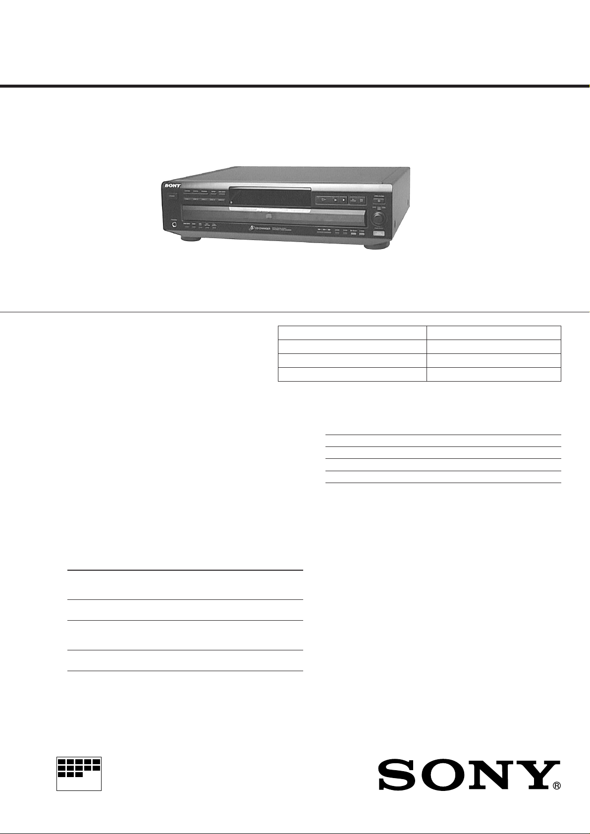
Photo : CDP-CE515
Model Name Using Similar Mechanism CDP-C360Z/CE415
CD Mechanism Type CDM27G-5BD22
Base Unit Type BU-5BD22
Optical Pick-up Type KSS-213BA/F-NP
SPECIFICATIONS
US Model
CDP-C460Z/CE515
Canadian Model
AEP Model
Australian Model
CDP-CE515
Compact Disc Player
Laser Semiconductor laser (λ = 780 nm)
Laser output Max 44.6 µW*
Frequency response 2 Hz to 20 kHz ± 0.5 dB
Signal-to-noise ratio More than 107 dB
Dynamic range More the 98 dB
Harmonic distortion Less than 0.0035%
Output
LINE OUT Phono 2V
DIGITAL OUT Optical –18 dBm Wave length:
(OPTICAL) output 660 nm
PHONES Stereo 10 mW 32 ohms
Emission duration: continuous
* This output is the value measured at a
distance of 200 mm from the objective
lens surface on the Optical Pick-up
block with 7 mm aperture.
Jack Maximum Load
type output impedance
level
Over 10 kilohms
jacks (at 50 kilohms)
connector
phone jack
General
Power requirements
Where purchased Power requirements
USA/Canada 120 V AC, 60 Hz
Europe 220 V – 230 V AC, 50/60 Hz
Australia 240 V AC, 50/60 Hz
Power consumption 14W
Dimensions (approx.) 430 × 120 × 393 mm
(w/h/d) (17 × 4 3/4 × 15 1/2 in.) incl. projecting parts
Mass (approx.) 5.4 kg (11 lbs 15 oz)
Supplied accessories
Audio cord (2 phono plugs–2 phono plugs) (1)
Remote commander (remote)(1)
Sony SUM-3 (NS) batteries (2)
Design and specifications are subject to change without notice.
COMPACT DISC PLAYER
MICROFILM
Page 2
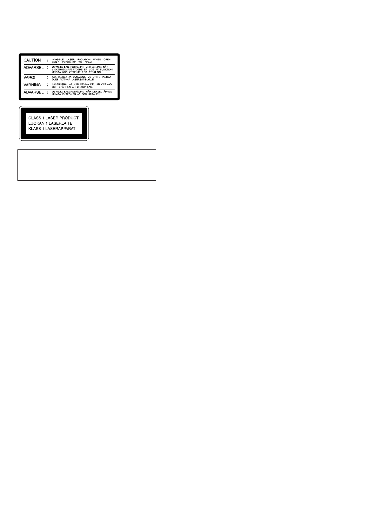
The following caution label is located inside of the unit.
http://www.jdwxzlw.com/?fromuser=华盛维修
家电维修资料网,免费下载各种维修资料
TABLE OF CONTENTS
1. GENERAL ..................................................................... 7
2. DISASSEMBLY
2-1. Case, Bottom Plate and Front Panel ··································· 8
2-2. Back Panel and Disc Table ················································· 8
2-3. Optical Pick-up Block Assembly ······································· 9
2-4. Bracket (Gear) Assembly ··················································· 9
This appliance is classified
as a CLASS 1 LASER
product.
The CLASS 1 LASER
PRODUCT MARKING is
located on the rear exterior.
CAUTION
Use of controls or adjustments or performance of procedures
other than those specified herein may result in hazardous
radiation exposure.
3. ELECTRICAL BLOCK CHECKING................... 10
4. DIAGRAMS
4-1. Circuit Boards Location ··················································· 12
4-2. Printed Wiring Board — BD Section —·························· 13
4-3. Schematic Diagram — BD Section —····························· 15
4-4. Printed Wiring Board — Main Section — ······················· 17
4-5. Schematic Diagram — Main Section — ·························· 19
4-6. Schematic Diagram — Display Section — ······················ 21
4-7. Printed Wiring Board — Display Section — ··················· 23
4-8. IC Block Diagrams ··························································· 25
4-9 IC Pin Functions
• IC101 Digital Signal Processor (CXD2545Q)···············27
• IC302 System Control (CXP84340-060Q) ···················· 30
5. EXPLODED VIEWS
5-1. Front Panel and Case Section ··········································· 32
5-2. Back Panel and Disc Table Section ·································· 33
5-3. Chassis Section································································· 34
5-4. Base Unit Section (BU-5BD22) ······································· 35
6. ELECTRICAL PARTS LIST ................................... 36
SAFETY-RELATED COMPONENT WARNING!!
COMPONENTS IDENTIFIED BY MARK ! OR DOTTED LINE WITH
MARK ! ON THE SCHEMATIC DIAGRAMS AND IN THE PARTS
LIST ARE CRITICAL TO SAFE OPERATION. REPLACE THESE
COMPONENTS WITH SONY PARTS WHOSE PART NUMBERS
APPEAR AS SHOWN IN THIS MANUAL OR IN SUPPLEMENTS
PUBLISHED BY SONY.
ATTENTION AU COMPOSANT AYANT RAPPORT
À LA SÉCURITÉ!
LES COMPOSANTS IDENTIFÉS P AR UNE MARQUE ! SUR LES
DIAGRAMMES SCHÉMA TIQUES ET LA LISTE DES PIÈCES SONT
CRITIQUES POUR LA SÉCURITÉ DE FONCTIONNEMENT. NE
REMPLACER CES COMPOSANTS QUE PAR DES PIÈSES SONY
DONT LES NUMÉROS SONT DONNÉS DANS CE MANUEL OU
DANS LES SUPPÉMENTS PUBLIÉS PAR SONY.
— 2 —
Page 3
MODEL IDENTIFICATION
http://www.jdwxzlw.com/?fromuser=华盛维修
家电维修资料网,免费下载各种维修资料
— BACK PANEL —
4-987-
CDP-CE515
US Model : 842-0π
CDP-CE515
Canadian Model : 842-1π
CDP-CE515
AEP Model : 842-2π
CDP-C460Z
US Model : 842-3π
CDP-CE515
Australian Model : 842-5π
NOTES ON HANDLING THE OPTICAL PICK-UP
BLOCK OR BASE UNIT
The laser diode in the optical pick-up block may suffer electrostatic
breakdown because of the potential difference generated by the
charged electrostatic load, etc. on clothing and the human body.
During repair, pay attention to electrostatic breakdo wn and also use
the procedure in the printed matter which is included in the repair
parts.
The flexible board is easily damaged and should be handled with
care.
SAFETY CHECK-OUT
(US model only)
After correcting the original service problem, perform the
following safety checks before releasing the set to the customer:
Check the antenna terminals, metal trim, “metallized” knobs, screws,
and all other exposed metal parts for A C leakage. Check leakage as
described below.
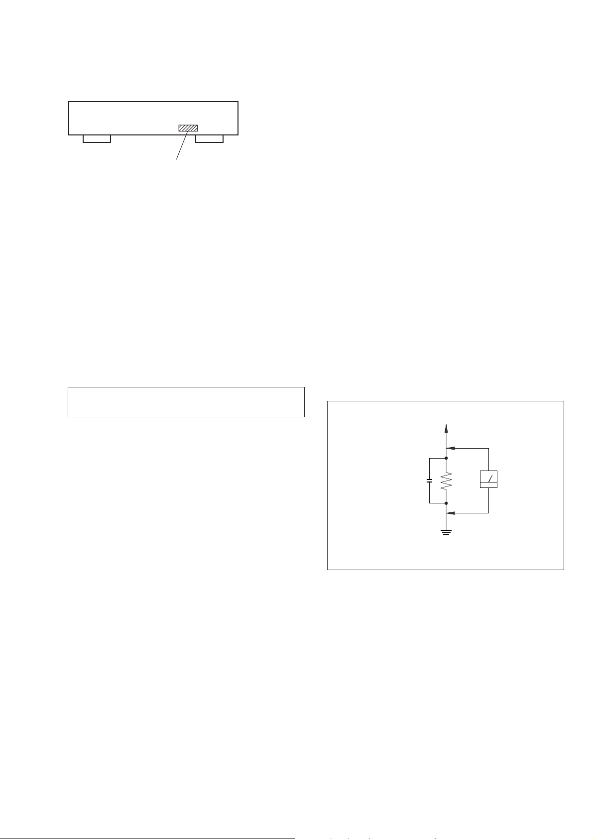
LEAKAGE
The A C leakage from any exposed metal par t to earth ground and
from all exposed metal parts to any exposed metal part having a
return to chassis, must not exceed 0.5 mA (500 microampers).
Leakage current can be measured by any one of three methods.
1. A commercial leakage tester , such as the Simpson 229 or RCA
WT -540A. Follo w the manufacturers’ instructions to use these
instruments.
2. A battery-operated AC milliammeter. The Data Precision 245
digital multimeter is suitable for this job.
3. Measuring the voltage drop across a resistor by means of a
VOM or battery-operated AC v oltmeter . The “limit” indication
is 0.75 V, so analog meters must have an accurate low-voltage
scale. The Simpson 250 and Sanwa SH-63Trd ar e examples of
a passive VOM that is suitable. Nearly all battery operated
digital multimeters that have a 2V AC range are suitable. (See
Fig. A)
To Exposed Metal
Parts on Set
AC
0.15µF
1.5k
Ω
voltmeter
(0.75V)
NOTES ON LASER DIODE EMISSION CHECK
The laser beam on this model is concentrated so as to be focused on
the disc reflective surface by the objective lens in the optical pickup block. Therefore, when checking the laser diode emission,
observe from more than 30 cm away from the objective lens.
Earth Ground
Fig. A. Using an AC voltmeter to check AC leakage.
— 3 —
Page 4
CD-TEXT TEST DISC
http://www.jdwxzlw.com/?fromuser=华盛维修
家电维修资料网,免费下载各种维修资料
This unit is able to display the test data (character information) written in the CD on its fluorescent indicator tube.
The CD-TEXT TEST DISC (TGCS-313:4-989-366-01) is used for checking the display.
To check, perform the following procedure.
Checking Method:
1. T urn ON the po wer , set the disc on the disc table with the side labeled as “test disc” as the right side, close the front cover , and c huck the
disc.
2. Press the ” button and play back the disc.
3. The following will be displayed on the fluorescent indicator tube.
Display : 1kHz/0 dB/ L&R
4. Press the = and + buttons to switch the track. The text data of each track will be displayed.
For details of the displayed contents for each track, refer to “T able 1 : CD-TEXT TEST DISC TEXT Data Contents” and “Table 2 : CDTEXT TEST DISC Recorded Contents and Display”.
Restrictions in CD-TEXT Display
In this unit, some special characters will not be displayed properly. These will be displayed as a space or a character resembling it. For details,
refer to “Table 2 : CD-TEXT DISC Recorded Contents and Display”.
Table 1 : CD-TEXT TEST DISC TEXT Data Contents (TRACKS No. 1 to 41:Normal Characters)
TRACK
No.
1
2
3
4
5
6
7
8
9
10
11
12
13
14
15
16
17
18
19
20
21
Displayed Contents
1kHz/0dB/L&R
20Hz/0dB/L&R
40Hz/0dB/L&R
100Hz/0dB/L&R
200Hz/0dB/L&R
500Hz/0dB/L&R
1kHz/0dB/L&R
5kHz/0dB/L&R
7kHz/0dB/L&R
10kHz/0dB/L&R
16kHz/0dB/L&R
18kHz/0dB/L&R
20kHz/0dB/L&R
1kHz/0dB/L&R
1kHz/-1dB/L&R
1kHz/-3dB/L&R
1kHz/-6dB/L&R
1kHz/-10dB/L&R
1kHz/-20dB/L&R
1kHz/-60dB/L&R
1kHz/-80dB/L&R
TRACK
No.
22
23
24
25
26
27
28
29
30
31
32
33
34
35
36
37
38
39
40
41
Displayed Contents
1kHz/-90dB/L&R
Infinity Zero w/o emphasis//L&R
Infinity Zero with emphasis//L&R
400Hz+7kHz(4:1)/0dB/L&R
400Hz+7kHz(4:1)/-10dB/L&R
19kHz+20kHz(1:1)/0dB/L&R
19kHz+20kHz(1:1)/-10dB/L&R
100Hz/0dB/L*
1kHz/0dB/L*
10kHz/0dB/L*
20kHz/0dB/L*
100Hz/0dB/R*
1kHz/0dB/R*
10kHz/0dB/R*
20kHz/0dB/R*
100Hz Squer Wave//L&R
1kHz Squer Wave//L&R
1kHz w/emphasis/-0.37dB/L&R
5kHz w/emphasis/-4.53dB/L&R
16kHz w/emphasis/-9.04dB/L&R
NOTE : The contents of Track No. 1 to 41 are the same as those of the current TEST DISC-their titles are displayed.
— 4 —
* Other channel is infinity zero.
Page 5
Table 2: CD-TEXT TEST DISC Recorded Contents and Display
http://www.jdwxzlw.com/?fromuser=华盛维修
家电维修资料网,免费下载各种维修资料
(In this unit, some special characters cannot be displayed. This is no a fault.)
TRACK
42
43
44
45
46
47
48
49
50
51
52
53
54
55
56
57
58
59
60
61
62
63
64
65
66
67
to
99
Recorded contents Display
! ” # $ %& ’ (21h to 27h)1kHz 0dB L&R
( ) + , – . / (28h to 2Fh)
*
01234567 (30h to 37h)
8 9 : ; < = > ? (38h to 3Fh)
@A B C D E F G (40h to 47h)
H I J K L MNO (48h to 4Fh)
P Q R S T U VW (50h to 57h)
X Y Z [ ¥ ] ^ _ (58h to 5Fh)
a b c d e f g (60h to 67Fh)
′
h i j k l m n o (68h to 6Fh)
p q r s t u v w (70h to 77h)
xyz{ I }
i ¢ £ ¤ ¥ § (A0h to A7h) 8859-1
¬
C ª
•±23
1
†
АБВГДЕЖЗ (C0h to C7h)
ИЙКЛМНОП (C8h to CFh)
D СТУФХЦ
ШЩЪЫЬY
абвгдежз (E0h to E7h)
ийклмноп (E8h to EFh)
∂ стуфхц÷ (F0h to F7h)
шщъыьy
No.66
No.67
to
No.99
PR
µ¶ • (B0h to B7h)
′
1
1
º ¿ (B8h to BFh)
2
4
˙
´
(78h to 7Fh)
~
–
(A8h to AFh)
3
4
(D0h to D7Fh)
ß (D8h to DFh)
ÿ (F8h to FFh)
N All the same
N All the same
N All the same
N All the same
N All the same
N All the same
N All the same
X Y Z [ ] ^ _ (58····
|| a b c d e f g (60····
N All the same
N All the same
xyz{I}–
A A A A A A C (C0···· Æ is not displayed
EEEEIIII (C8
D NOOOOO (D0····
O UU U U Y (D8····
a a a a a a c (E0···· æ is not displayed
eeeeiiii (E8····
d n o o o o o (F0···· ÷ is not displayed
o u u u u y y (F8····
N All the same
N All the same
N All the same
/
(78····
(A0···· All not displayed
(A8···· All not displayed
(B0···· All not displayed
(B8···· All not displayed
is not displayed
ß are not displayed
is not displayed
to
— 5 —
Page 6
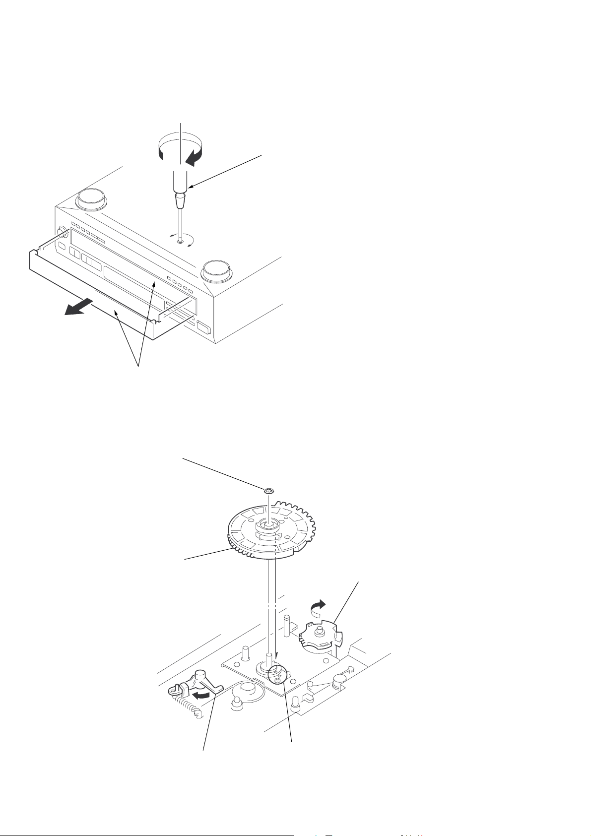
HOW TO OPEN THE DISC TRAY WHEN POWER
http://www.jdwxzlw.com/?fromuser=华盛维修
家电维修资料网,免费下载各种维修资料
SWITCH TURNS OFF
IN
OUT
Insert a tapering driver into the aperture of the unit bottom, and turn in
the direction of arrow (to OUT direction).
* To close the disc tray, turn the driver in the reverse direction
(to IN direction).
Tray
NOTE FOR MAIN GEAR INSTALLATION
5
Stopper washer (5)
4
Install the MAIN GEAR
as show in the drawing.
A
3
Rotate the GEAR (U/D)
to the arrow
A
direction.
B
1
Set the mark of
2
Slide the SET LEVER to the
arrow
B
direction.
ROTARY ENCODER.
— 6 —
Page 7
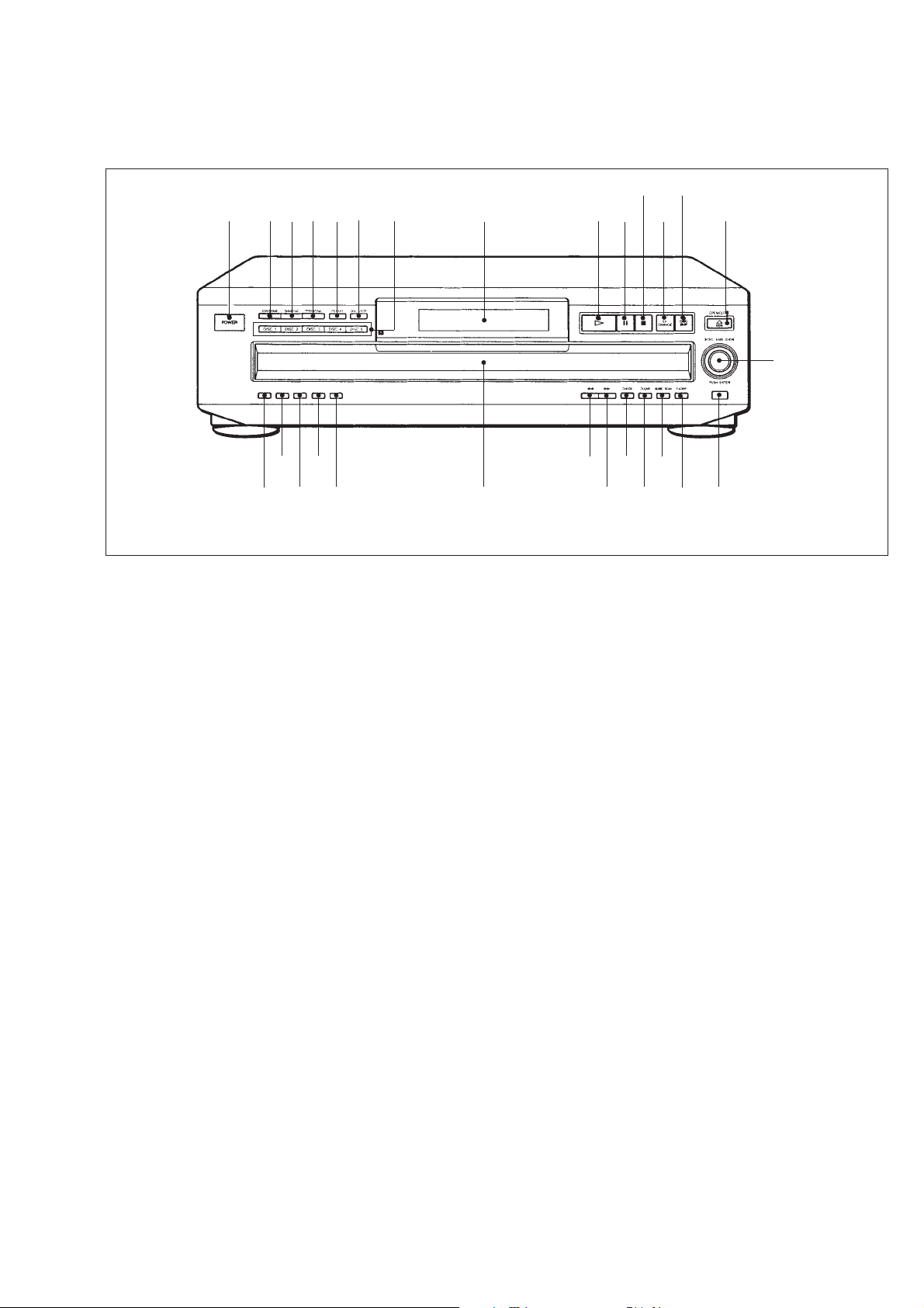
Identifying the Parts
http://www.jdwxzlw.com/?fromuser=华盛维修
家电维修资料网,免费下载各种维修资料
Front Panel
1
234
@¢
5
6
7
SECTION 1
GENERAL
8
90
@¡@§
!¡
!ª
!£
!™ !¢
!∞
!¶
@£
@∞@¶
1 POWER switch
2 CONTINUE button
3 SHUFFLE button
4 PROGRAM button
5 REPEAT button
6 TIME/TEXT button : C460Z model
DISC CHECK button : CE515 model
7 DISC 1-5 button
8 Display window
9 ” (play) button
!º P (pause) button
!¡ p (stop) button
!™ EX-CHANGE button
!£ DISC SKIP button
@™
!¢ 6 OPEN/CLOSE button
!∞ AMS knob
!§ X-FADE button
!¶ NO DELAY button
!• CLEAR button
!ª CHECK button
@º ) (forward) button
@¡ 0 (backward) button
@™ Disc tray
@£ PEAK SEARCH button: CE515 model
@¢ EDIT/TIME FADE button: CE515 model
@∞ TIME/TEXT button: CE515 model
@§ FADER button
@¶ MEMO INPUT button
@• MEGA CONTROL button
@º !•
!§
@•
— 7 —
Page 8
SECTION 2
http://www.jdwxzlw.com/?fromuser=华盛维修
家电维修资料网,免费下载各种维修资料
DISASSEMBLY
Note : Follow the disassembly procedure in the numerical order given.
2-1. CASE, BOTTOM PLATE AND FRONT PANEL
4
Case
1
Two screws
(M3
×
8)
!º
Two screws
(BVTT3
!™
Front panel
×
8)
9
Flat type wire (9 core)
(MAIN board, to CN403)
3
Two screws
(BV3
×
8)
2
Two screws
(M3
8
Flat type wire (17 core)
(MAIN board, to CN402)
×
8)
!¡
Three screws
(BVTP3
2-2. BACK PANEL AND DISC TABLE
!∞
Disc table (B)
!§
Disc table (A)
!£
Bracket
!º
Screw
(BVTP3
(guideB1)
×
8)
×
8)
!¡
Bracket (guide F1)
!™
Screw
(BVTP3
×
10)
5
Four screws
(BVTP3
!¢
Screw
(PTPWH3
×
10)
×
12)
7
Bottom plate
3
Back panel
4
6
Three screws
(BVTP3
Flat type wire (6 core)
(MAIN board, to CN404)
×
10)
2
Five screws
(BVTP3
1
Connector
×
10)
6
Bracket (guide B1)
5
9
Bracket (guide F1)
8
7
Screw (BVTP3 × 8)
Ground plate (chassis-R)
Screw
(BVTP3
×
8)
— 8 —
Page 9
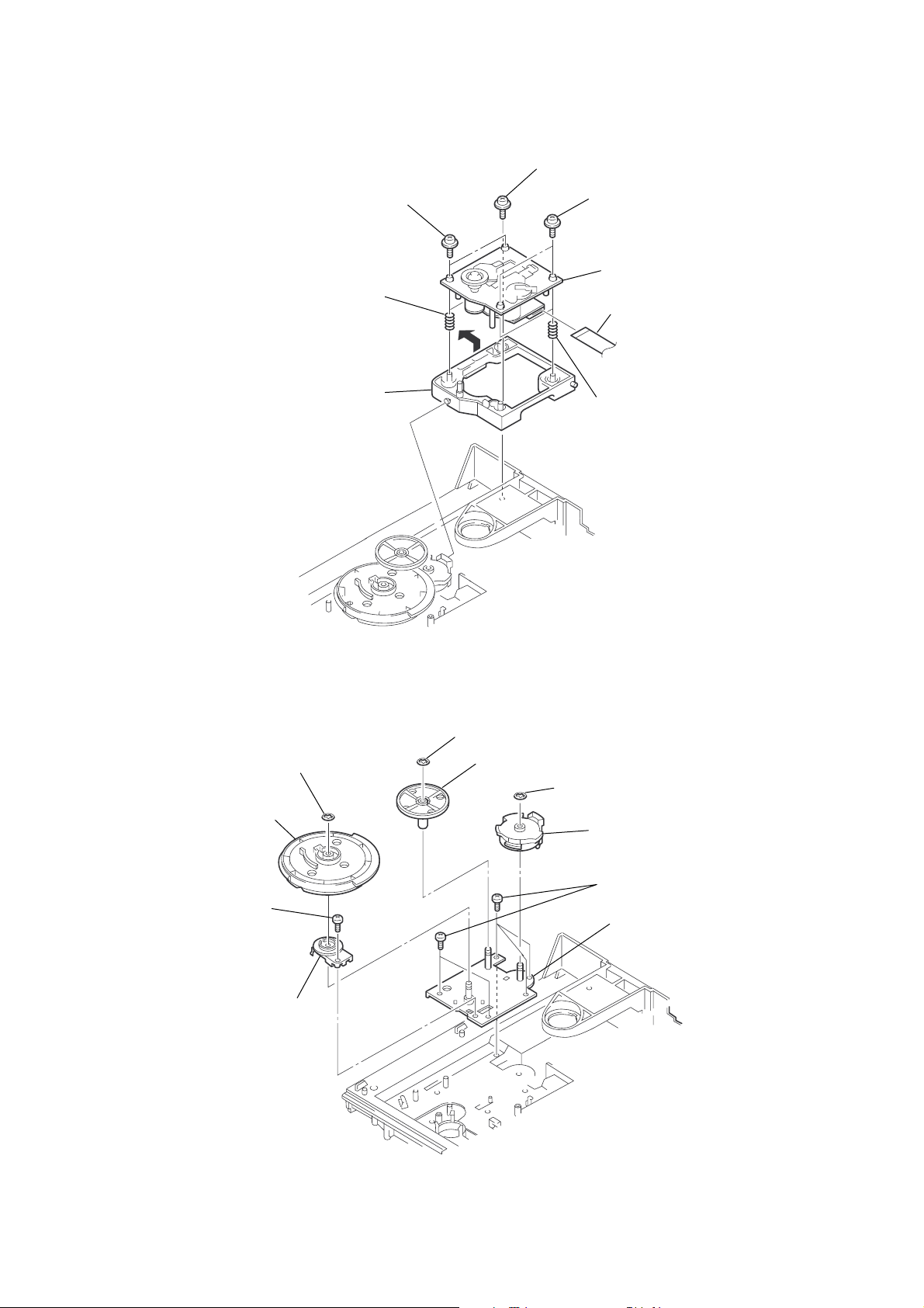
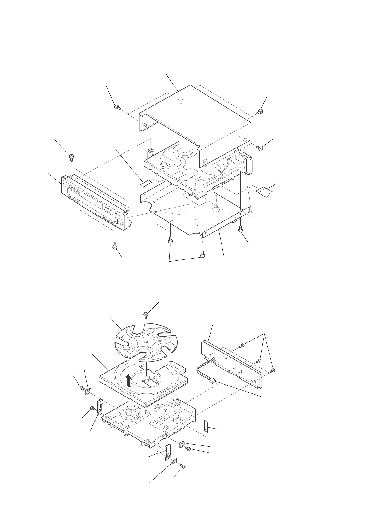
2-3. OPTICAL PICK-UP BLOCK ASSEMBLY
http://www.jdwxzlw.com/?fromuser=华盛维修
家电维修资料网,免费下载各种维修资料
3
Two screws
(PTPWH2.6
6
Compression spring (BU)
5
Holder (BU)
2
Screw
(PTPWH3
×
6)
×
12)
4
Two screws
(PTPWH2.6
8
Optical pick-up block assembly
1
Flat type wire (23 core)
(BD board, to CN101)
7
Compression spring (BU)
×
6)
2-4. BRACKET (GEAR) ASSEMBLY
3
Stopper washer (5)
4
Gear (MAIN)
5
Screw
(BVTP3
×
8)
6
Rotary encoder
1
Stopper washer (5)
2
Gear (REV)
7
Stopper washer (5)
8
Gear (U/D)
9
Five screws
(BVTP3
0
Bracket (GEAR)
assembly
×
8)
Note : As for the installation of the main gear, refer to “Note for MAIN
GEAR installation” on page 4.
— 9 —
Page 10
SECTION 3
http://www.jdwxzlw.com/?fromuser=华盛维修
家电维修资料网,免费下载各种维修资料
ELECTRICAL BLOCK CHECKING
Note :
1. CD Block is basically designed to operate without adjustment.
Therefore, check each item in order given.
2. Use YEDS-18 disc (3-702-101-01) unless otherwise indicated.
3. Use an oscilloscope with more than 10MΩ impedance.
4. Clean the object lens using an applicator with neutral detergent
when the signal level is low than specified value with the
following checks.
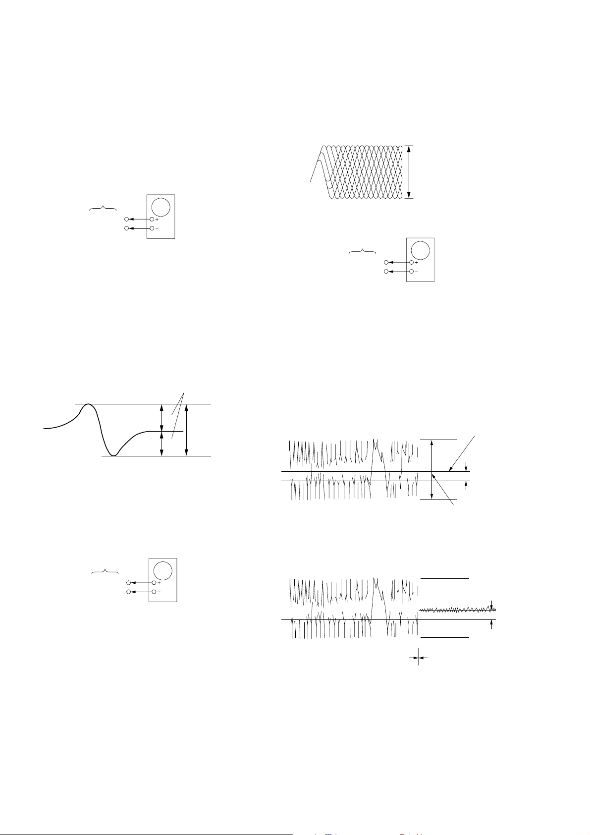
S Curve Check
oscilloscope
BD board
TP (FE)
TP (VC)
Procedure :
1. Connect oscilloscope to test point TP (FE) on BD board.
2. Connect between test point TP (FEI) and TP (VC) by lead wire.
3. Turn Power switch on.
4. Put disc (YEDS-18) in and turn Power switch on again and
actuate the focus search. (Actuate the focus search when disc
table is moving in and out.)
5. Check if the oscilloscope waveform (S-curve) is symmetrical
between A and B. And confirm peak to peak level within 3±1
Vp-p.
S-curve waveform
symmetry
Note :
A clear RF signal waveform means that the shape “ ◊ ” can
be clearly distinguished at the center of the waveform.
RF signal waveform
VOLT/DIV : 200mV
TIME/DIV : 500ns
level :
1.25 ± 0.25 Vp-p
E-F Balance Check
oscilloscope
BD board
TP (TE)
TP (VC)
Procedure :
1. Connect test point TP1 (ADJ) to ground with a lead wire.
2. Connect oscilloscope to test point TP (TE) on BD board.
3. Turned Power switch on.
4. Put disc (YEDS-18) in to play the number five track.
5. Press the “3” button. (The tracking servo and the sledding servo
are turned OFF.)
6. Check the level B of the oscilloscope's waveform and the A
(DC voltage) of the center of the Traverse waveform.
Confirm the following :
A/B × 100 = less than ± 22%
A
within 3 ± 1 Vp-p
B
6. After check, remove the lead wire connected in step 2.
Note : • Try to measure several times to make sure than the ratio
of A : B or B : A is more than 10 : 7.
• Take sweep time as long as possible and light up the
brightness to obtain best waveform.
RF Level Check
oscilloscope
BD board
TP (RF)
TP (VC)
Procedure :
1. Connect oscilloscope to test point TP (RF) on BD board.
2. Turned Power switch on.
3. Put disc (YEDS-18) in to play the number five track.
4. Confirm that oscilloscope waveform is clear and check if RF
signal level is correct or not.
Traverse waveform
Center of the waveform
B
0V
level : 1.3 ± 0.6 Vp-p
7. Press the “8” button. (The tracking servo and sledding servo
are turned ON.) Confirm the C (DC voltage) is almost equal to
the A (DC voltage) is step 6.
Traverse waveform
0V
Tracking servo
Sledding servo
OFF
8. Disconnect the lead wire of test point TP1 (ADJ) connected in
step 1.
Tracking servo
Sledding servo
A (DC voltage)
ON
C (DC
voltage)
— 10 —
Page 11
RF PLL Free-run Frequency Check
http://www.jdwxzlw.com/?fromuser=华盛维修
家电维修资料网,免费下载各种维修资料
Procedure :
1. Connect frequency counter to test point TP (PLCK) with lead
wire.
BD board
TP (PLCK)
2. Turned Power switch on.
3. Put the disc (YEDS-18) in to play the number five track.
Confirm that reading on frequency counter is 4.3218MHz.
frequency counter
Adjustment Location :
[ BD BOARD ] — Conductor Side —
1
20
(FE)
(FEI)
(RF)
IC103
11
10
(PLCK)
(TE)
(VC)
IC101
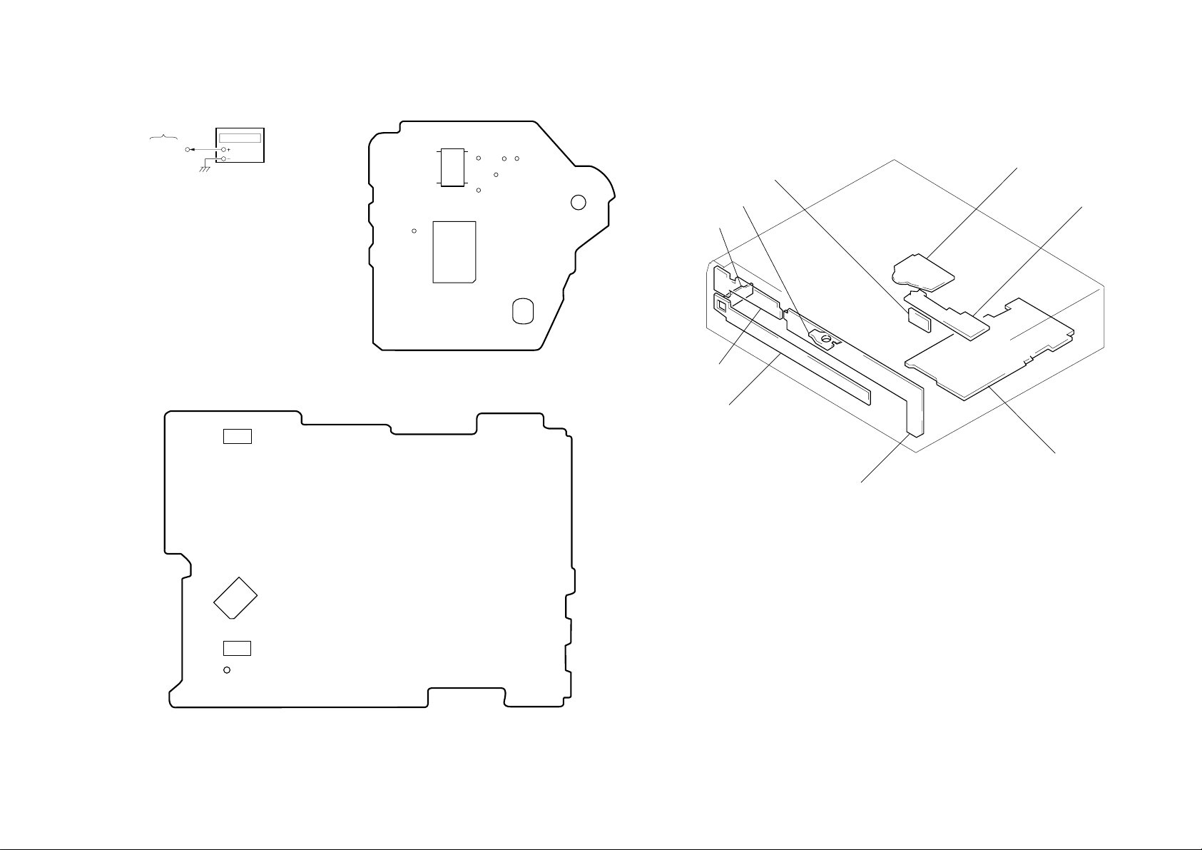
4-1. CIRCUIT BOARDS LOCATION
TABLE MOTOR BOARD
LOADING MOTOR BOARD
HP BOARD
CDP-C460Z/CE515
SECTION 4
DIAGRAMS
BD BOARD
SENSOR BOARD
[ MAIN BOARD ] — Conductor Side —
80
1
IC302
40 41
TP1
(ADJ)
65
64
24
25
POWER SW BOARD
KEY BOARD
MAIN BOARD
DISPLAY BOARD
— 11 — — 12 —
Page 12

http://www.jdwxzlw.com/?fromuser=华盛维修
家电维修资料网,免费下载各种维修资料
Page 13

http://www.jdwxzlw.com/?fromuser=华盛维修
家电维修资料网,免费下载各种维修资料
Page 14

http://www.jdwxzlw.com/?fromuser=华盛维修
家电维修资料网,免费下载各种维修资料
Page 15

http://www.jdwxzlw.com/?fromuser=华盛维修
家电维修资料网,免费下载各种维修资料
Page 16

http://www.jdwxzlw.com/?fromuser=华盛维修
家电维修资料网,免费下载各种维修资料
Page 17

http://www.jdwxzlw.com/?fromuser=华盛维修
家电维修资料网,免费下载各种维修资料
Page 18

CDP-C460Z/CE515
1INIT
2
3
4
5
6
7
8
9
10
11
12
13
14
D Vdd 2
SYSM L1 (+)
ATT A Vdd L
SHIFT L2 (+)
LATCH A Vss L
256FSO X Vss
TEST1 512IN
D Vss X OUT
MCKSEL X Vdd
XBCK A Vss R
DATA R2 (+)
LRCK A Vdd R
MUTE L R1 (+)
MUTE R D Vdd 1
28
27
26
25
24
23
22
21
20
19
18
17
16
15
MODES/P
ATT
IIR
FIR3FIR2FIR1
PLMPLM
MUTE
CIRCUIT
CLOCK
GENERATOR
AC
DITHER
DC
DITHER
3RD ORDER
NOISE SHAPER
SAMPLE
HOLD (X1)
TIMING CIRCUIT
http://www.jdwxzlw.com/?fromuser=华盛维修
家电维修资料网,免费下载各种维修资料
4-8. IC BLOCK DIAGRAMS
IC101 CXD2545Q
VPCO20VCKI
XTSL63XTAO62XTAI67FSTO
19
C4M
68
C16M
69
PDO
18
13
VCO1
12
VCO0
PCO
33
32
FILI
31
FILO
CLTV
34
36
RFAC
ASYMMETRY
ASYI
38
CORRECTION
39
ASYO
ASYE
42
WFCK
73
SCOR
74
EXCK
76
75
SBSO
72
EMPH
SQCK
78
77
SQSO
95
MON
FSW
94
96
MDP
MDS
97
26
RFDC
TE
27
28
SE
FE
29
VC
30
25
BUFF
1CH1 OUT F
BUFF
2CH1 OUT R
3CAPA IN 1
R
4CH1 R IN
F
5CH1 F IN
6VREF IN
7VREF OUT
8GND
FF
9CH2 F IN
RR
10CH2 R IN
11CAPA IN 2
BUFF BUFF
12CH2 OUT R
BUFF
13CH2 OUT F
14GND
64
CLOCK
GENERATOR
DIGITAL
PLL
VARI-PITCH
DOUBLE SPEED
MUX
GENERATOR 1
SUBCODE
P-W
PROCESSOR
SUBCODE
0
PROCESSOR
18-TIMES
NOISE
OVERSAMPLING
SHAPER
SWITCH
&
BUFFER
24 141617 35 66 82 83 84
RFC
ADIO
TEST
INTERFACE
INTERFACE INTERFACE
TIMING
FILTER
A / D
CONVERTER
TES2
TES3
EFM
DEMODULATOR
SYNC
PROTECTOR
PROCESSOR
214023
AVSS
AVDD
AVDD
F
R
BUFF
RRFF
CLV
MIRR
DFCT
FOK DETECTOR
419015
ADD
AVSS
RESISTER
ERROR CORRECTOR
FOCUS SERVO
ADD
LEVEL
SHIFT
GENERATOR 2
MICRO PROGRAM
INTERFACE
SERVO DSP
SLED SERVO
TRACKING
SERVO
8165
XRST
DVSS
DVSS
MUTE
32K RAM
ADRESS
PRIORITY
GENERATOR
ENCODER
D / A
DATA PROCESSOR
PEAK DETECTOR
DIGITAL OUT
CPU INTERFACE
TIMING
SERVO
PWM GENERATOR
SLED PWM
GENERATOR
TRACKING PWM
GENERATOR
FOCUS PWM
GENERATOR
22 37 44 45
FSTI
BIAS
IGEN
BUFF
BUFF
BUFF
DIRC
LRCK
WDCK
28 GND
27 CH4 OUT F
26 CH4 OUT R
25 VB IN
24 VS IN
23 VB IN
22 VCC
21 VCC
20 CH3 F IN
19 CH3 R IN
18 CAPA IN 3
17 CH3 OUT R
16 CH3 OUT F
15 MUTE
— 25 — — 26 —
SERIAL
PARALLEL
PROCESSOR
SERVO
AUTO
SEQUENCER
SCLK
OFSW
PSSL
43
16
ATSK
DA01-16
61 - 46
MUTE
79
D OUT
71
MD2
70
DATA
86
CLOK
88
XLAT
87
SENS
80
COUT
89
MIRR
91
DFCT
92
FOK
93
2
SFON, SFDR
3, 100
2
1, 2
SRON, SRDR
2
4, 7
TFDR, TFON
2
5, 6
TRON, TRDR
2
FFDR, FFON
8, 11
2
4, 7
TRON, FRDR
9, 10
999885
SSTP
LOCK
1
LD VCCVCC
2
PD LD ON
3
A LC/PD
4
B RFE
5
C RFO
D FE
6
VEE FE BIAS
7
8
F TE
9
E VC
EI EO
10
VEE
VC
VC
VEE
VC
RF SUMMING AMP
IC301 CXD8567AM IC603 M5293L
20
19
18
17
16
15
14
13
VC
12
11
VREF
VCC
VEE
VC
VEE
APC LD AMP
FOCUS ERROR AMP
TRACKING ERROR AMP
VC
VC
VCC
RF EQ AMP
VC
VC BUFFER
IC601 LA5602IC103 CXA1821MIC102 BA6392FP
CDEL
V OUT
GND
2
5k
REFERENCE
4
ON/OFF
VOLTAGE
1
IN
1
V IN
REFERENCE
VOLTAGE
OVER CURRENT
LIMITTER
OVER HEAT
PROTECTION
2
EN
GND
RES
CN
ON/OFF
RESET
3
GEN
4
5
6
7
ERROR
AMP
+
–
OVERHEAT
PROTECTION
27k
OVERCURRENT
LIMITTER
5
3
REFERENCE
VOLTAGE
OUT
Page 19

4-9. IC PIN FUNCTIONS
http://www.jdwxzlw.com/?fromuser=华盛维修
家电维修资料网,免费下载各种维修资料
• IC101 DIGITAL SIGNAL PROCESSOR (CXD2545Q)
Pin No.
1
2
3
4
5
6
7
8
9
10
11
12
13
14
15
16
17
18
19
20
21
22
23
24
25
26
27
28
29
30
31
32
33
34
35
36
37
38
39
40
SRON
SRDR
SFON
TFDR
TRON
TRDR
TFON
FFDR
FRON
FRDR
FFON
VCOO
VCOI
TEST
DVss
TES2
TES3
PDO
VPCO
VCKI
AVD2
IGEN
AVS2
ADIO
RFC
RFDC
TE
SE
FE
VC
FILO
FILI
PCO
CLTV
AVS1
RFAC
BIAS
ASYI
ASYO
AVD1
Pin Name
I/O
Sled drive output (Not used)
O
Sled drive output
O
Sled drive output (Not used)
O
Tracking drive output
O
Tracking drive output (Not used)
O
Tracking drive output
O
Tracking drive output (Not used)
O
Focus drive output
O
Focus drive output (Not used)
O
Focus drive output
O
Focus drive output (Not used)
O
VCO output for analog EFM PLL (Not used)
O
VCO input for analog EFM PLL (Ground)
I
TEST pin connected normally to ground
I
Digital ground
—
TEST pin connected normally to ground
I
TEST pin connected normally to ground
I
Charge-pump output for analog EFM PLL (Not used)
O
Charge-pump output for variable pitch PLL (Not used)
O
Clock input from variable pitch external VCO (Ground)
I
Analog power supply
—
Power supply pin for operational amplifiers
I
Analog ground
—
(Not used)
I
(Not used)
O
RF signal input
I
Tracking error signal input
I
Sled error signal input
I
Focus error signal input
I
Center voltage input pin
I
Filter output for master PLL
O
Filter input for master PLL
I
Charge-pump output for master PLL
O
Control voltage input for master VCO
I
Analog ground
—
EFM signal input
I
Asymmetry circuit constant current input
I
Asymmetry comparate voltage input
I
EFM full swing output
O
Analog power supply
—
Function
— 27 —
Page 20

Pin No.
http://www.jdwxzlw.com/?fromuser=华盛维修
家电维修资料网,免费下载各种维修资料
41
42
43
44
45
46
47
48
49
50
51
52
53
54
55
56
57
58
59
60
61
62
63
64
65
66
67
68
69
70
71
72
73
74
75
76
77
78
79
80
DD
DV
ASYE
PSSL
WDCK
LRCK
DATA
BCLK
64DATA
64BCLK
64LRCK
GTOP
XUGF
XPLCK
GFS
RFCK
C2PO
XRAOF
MNT3
MNT2
MNT1
MNT0
XTAI
XTAO
XTSL
DVss
FSTI
FSTO
FSOF
C16M
MD2
DOUT
EMPH
WFCK
SCOR
SBSO
EXCK
SUBQ
SQCK
MUTE
SENS
Pin Name
I/O
Digital power supply
—
Asymmetry circuit ON/OFF
I
Audio data output mode selection input
I
48-bit slot D/A interface. Word clock.
O
48-bit slot D/A interface. LR clock.
O
DA 16 output when PSSL=1.48-bit slot serial data when PSSL=0
O
DA 15 output when PSSL=1.48-bit slot data when PSSL=0
O
DA 14 output when PSSL=1.64-bit slot data when PSSL=0 (Not used)
O
DA 13 output when PSSL=1.64-bit slot data when PSSL=0 (Not used)
O
DA 12 output when PSSL=1.64-bit slot data when PSSL=0 (Not used)
O
DA 11 output when PSSL=1.GTOP output when PSSL=0 (Not used)
O
DA 10 output when PSSL=1.XUGF output when PSSL=0 (Not used)
O
DA 09 output when PSSL=1.XPLCK output when PSSL=0 (Not used)
O
DA 08 output when PSSL=1.GFS output when PSSL=0 (Not used)
O
DA 07 output when PSSL=1.RFCK output when PSSL=0 (Not used)
O
DA 06 output when PSSL=1.C2PO output when PSSL=0 (Not used)
O
DA 05 output when PSSL=1.XRA0F output when PSSL=0 (Not used)
O
DA 04 output when PSSL=1.MNT3 output when PSSL=0 (Not used)
O
DA 03 output when PSSL=1.MNT2 output when PSSL=0 (Not used)
O
DA 02 output when PSSL=1.MNT1 output when PSSL=0 (Not used)
O
DA 01 output when PSSL=1.MNT0 output when PSSL=0 (Not used)
O
X'tal oscillator circuit input
I
X'tal oscillator circuit output (Not used)
O
X'tal selection input pin (Ground)
I
Digital ground
—
2/3 divider input of pins 62, 63
I
2/3 divider output of pins 62, 63
O
(Not used)
O
16.9344 MHz output (Not used)
O
Digital-out ON/OFF control pin (+5V)
I
Digital-out output pin
O
Playback disc output in emphasis mode (Not used)
O
WFCK output
O
Sub-code sync output
O
Sub-P through Sub-W serial output
O
Clock input for SBS0 read-out (Ground)
I
Sub-Q 80-bit output
O
Sub-code Q clock output
O
Muting selection pin
I
SENS output
O
Function
— 28 —
Page 21

Pin No.
http://www.jdwxzlw.com/?fromuser=华盛维修
家电维修资料网,免费下载各种维修资料
81
82
83
84
85
86
87
88
89
90
91
92
93
94
95
96
97
98
99
100
Pin Name
XRST
DIRC
SCLK
DFSW
ATSK
DATA
XLAT
CLOK
COUT
DD
DV
MIRR
DFCT
FOK
FSW
MON
MDP
MDS
LOCK
SSTP
SFDR
I/O
System reset
I
Used in 1-track jump mode (+5v)
I
SENS serial data read-out clock
I
DFCT selection pin (Ground)
I
Input pin for anti-shock (Ground)
I
Serial data input, supplied from CPU
I
Latch input, supplied from CPU
I
Serial data transfer clock input, supplied from CPU
I
Numbers of track counted signal output (Not used)
O
Digital power supply
—
Mirror signal output (Not used)
O
Defect signal output (Not used)
O
Focus OK output (Not used)
O
Output to select spindle motor output filter (Not used)
O
Output to control ON/OFF of spindle motor (Not used)
O
Output to control spindle motor servo
O
Output to control spindle motor servo (Not used)
O
GFS is sampled by 460 Hz. H when GFS is H (Not used)
O
Input signal to detect disc inner most track
I
Sled drive output
O
Function
— 29 —
Page 22

• IC302 SYSTEM CONTROL (CXP84340-060Q)
http://www.jdwxzlw.com/?fromuser=华盛维修
家电维修资料网,免费下载各种维修资料
Pin No.
1
2
3
4
5
6
7
8
9
10
11
12
13
14
15
16
17
18
19
20
21
22
23
24
25
26
27
28
29
30
31
32
33
34
35
36
37
38
39
40
Pin Name
D3
D4
D2
D1
D0
A8
A7
A6
A5
A4
A3
A2
A1
PLAY_L
PAUSE_L
MEGA_L
XFADE_
MODELAY_L
WE
LODIN
LODOUT
FLCKL
FLDATA
BLK
A13
A14
NC
D.SENS
NC
RESET
10MHz
10MHz
GND
NC
NC
NC
NC
BUSOUT
VER
KEY6
I/O
I/O
SRAM data 3
I/O
SRAM data 4
I/O
SRAM data 2
I/O
SRAM data 1
I/O
SRAM data 0
O
SRAM address 8
O
SRAM address 7
O
SRAM address 6
O
SRAM address 5
O
SRAM address 4
O
SRAM address 3
O
SRAM address 2
O
SRAM address 1
O
PLAY lamp
O
PAUSE lamp
O
MEGA lamp
O
XFADE lamp
O
NO DELAY lamp
O
SRAM enable
O
Loading direction signal input
O
Loading direction signal output
O
Display clock
O
Display data
O
Display reset
—
SRAM address 13
—
SRAM address 14
—
Not used.
I
Disc exist/non-exist sensor
—
Not used.
I
Microprocessor reset
—
Ceramic oscillator
—
Ceramic oscillator
—
Ground (0V)
—
Not used.
—
Not used.
—
Not used.
—
Not used.
O
Control A1 output
I
Model selection
I
Key input 6
Function
— 30 —
Page 23

Pin No.
http://www.jdwxzlw.com/?fromuser=华盛维修
家电维修资料网,免费下载各种维修资料
41
42
43
44
45
46
47
48
49
50
51
52
53
54
55
56
57
58
59
60
61
62
63
64
65
66
67
68
69
70
71
72
73
74
75
76
77
78
79
80
Pin Name
KEY3
CD123
KEY2
KEY1
TEST
SENSOR
FLT
CLK
LDON
DATA
SQCLK
SUBQ
PRGL
SENSE
NC
RMIN
NC
XLT
AMUTE
DQSY
SCOR
BUSIN
TCLK
SMUTE
TDATA
ENC1
ENC2
ENC3
TBLL
TBLR
A0
+5V
+5V
A12
A11
A10
A9
D7
D6
D5
I/O
I
Key input 3
I
Command mode switch
I
Key input 2
I
Key input 1
I
Test mode terminal
I
Table sensor
O
Display latch
O
Command clock
O
Laser diode ON
O
Command data
O
Sub-Q clock
I
Sub-Q data
O
Digital filter latch
I
Sense
—
Not used.
I
Command latch
—
Not used.
—
Remote control signal input
O
Audio system mute
I
CD-TEXT sync signal
I
Sub-Q sync signal
I
Control-A input
O
CD-TEXT clock
O
2nd input mute
I
CD-TEXT data
I
Loading encoder 1
I
Loading encoder 2
I
Loading encoder 3
O
Rotation direction of table-L
O
Rotation direction of table-R
O
SRAM address 0
—
Microprocessor power supply (5V)
—
Microprocessor power supply (5V)
O
SRAM address 12
O
SRAM address 11
O
SRAM address 10
O
SRAM address 9
I/O
SRAM data 7
I/O
SRAM data 6
I/O
SRAM data 5
Function
— 31 —
Page 24

NOTE:
http://www.jdwxzlw.com/?fromuser=华盛维修
家电维修资料网,免费下载各种维修资料
• -XX, -X mean standardized parts, so they
may have some differences from the original
one.
• Items marked “*” are not stocked since they
are seldom required for routine service.
Some delay should be anticipated when
ordering these items.
• The mechanical parts with no reference number
in the exploded views are not supplied.
• Hardware (#mark) list is given in the last of
this parts list.
• Abbreviation
AUS : Australian
CND : Canadian
5-1. FRONT PANEL AND CASE SECTION
SECTION 5
EXPLODED VIEWS
The components identified by mark ! or
dotted line with mark ! are critical for safety .
Replace only with part number specified.
Les composants identifiés par une marque
! sont critiques pour la sécurité.
Ne les remplacer que par une pièce portant
le numéro spécifie.
11
12
13
#2
not supplied
23
5
24
18
#1
4
2
20
3
16
8
17
26
19
5
6
5
9
27
7
1
22
10
21
#1
15
5
5
14
#1
#1
5
not supplied
#1
13
25
Ref. No. Part No. Description Remarks Ref. No. Part No. Description Remarks
1 4-987-780-11 PANEL, LOADING
2 4-987-779-11 WINDOW (FL)
3 4-977-589-01 BUTTON (POWER)
4 3-008-600-01 EMBLEM (5-AR), SONY
5 4-951-620-01 SCREW (2.6X8), +BVTP
* 6 A-4699-620-A DISPLAY BOARD, COMPLETE
7 1-782-219-11 WIRE (FLAT TYPE) (17 CORE)
* 8 1-665-357-11 POWER SW BOARD
9 1-782-220-11 WIRE (FLAT TYPE) (9 CORE)
10 4-987-773-51 PANEL, FRONT (CE515)
10 4-987-773-61 PANEL, FRONT (C460Z)
* 11 4-978-492-11 CASE
12 3-703-685-21 SCREW (+BV 3X8)
13 3-704-366-01 SCREW (CASE) (M3X8)
14 X-4946-618-1 FOOT ASSY (US,CND)
14 X-4946-641-1 FOOT ASSY (AEP,AUS)
* 15 4-978-398-21 CUSHION
* 16 1-665-358-11 KEY BOARD
17 4-987-775-11 BUTTON (PLAY)
18 4-987-776-01 BUTTON (FUNC)
19 4-987-777-01 BUTTON (FF)
20 4-987-774-01 BUTTON (MODE)
21 4-987-994-01 KNOB (AMS)
22 4-987-778-01 BUTTON (MEGA-CON)
* 23 1-665-359-11 HP BOARD
* 24 4-979-090-01 BRACKET (HP)
25 4-977-593-01 RING (DIA. 50), ORNAMENTAL(AEP,AUS)
26 4-989-723-01 INDICATOR (PLAY)
27 4-989-725-01 BUTTON (X-FADE)
— 32 —
Page 25

5-2. BACK PANEL AND DISC TABLE SECTION
http://www.jdwxzlw.com/?fromuser=华盛维修
家电维修资料网,免费下载各种维修资料
#3
52
not
supplied
53
65
67
64
63
not supplied
#6
#4
51
66
not supplied
#4
63
54
72
64
#4
63
73
not
supplied
#5
64
62
63
60
61
#4
71
M801
55
57
58
AEP MODEL
56
US, CND
MODEL
AUS MODEL
59
70
#1
#1
59
59
#1
#4
not supplied
69
#4
not supplied
Ref. No. Part No. Description Remarks Ref. No. Part No. Description Remarks
51 4-957-299-11 TABLE (B), DISC
52 4-957-304-01 BELT (RM)
53 X-4943-479-1 GEAR (ROTARY A) ASSY
* 54 1-647-362-11 SENSOR BOARD
* 55 1-647-364-11 TABLE MOTOR BOARD
56 3-325-697-01 WASHER
57 4-957-284-01 GEAR (ROTARY B)
58 X-4943-477-1 BRACKET (RM) ASSY
! 59 1-575-651-21 CORD, POWER (AEP)
! 59 1-590-926-11 CORD, POWER (US,CND)
! 59 1-696-845-11 CORD, POWER (AUS)
60 4-957-293-01 SPRING (RACK RELEASE)
61 4-957-291-11 LEVER (RACK RELEASE)
62 4-957-868-01 SCREW (+PTPWH 2.6X20)
#4
63 4-988-162-01 ROLLER
64 4-934-376-01 SHAFT (ROLLER)
65 4-957-292-11 SLIDER (RACK)
66 4-957-294-01 SPRING (D.T), TENSION
67 4-957-298-01 TABLE (A), DISC
* 69 4-951-619-01 CUSHION (A)
* 70 3-703-244-00 BUSHING (2104), CORD
* 71 4-987-842-01 PANEL, BACK (CE515:US)
* 71 4-987-842-11 PANEL, BACK (CE515:CND)
* 71 4-987-842-21 PANEL, BACK (CE515:AEP)
* 71 4-987-842-31 PANEL, BACK (C460Z:US)
* 71 4-987-842-51 PANEL, BACK (CE515:AUS
72 1-751-052-11 WIRE (FLAT TYPE) (6 CORE)
73 X-4943-480-1 BRACKET (ROLLER D) ASSY
M801 A-4660-525-A MOTOR ASSY, ROTARY (TABLE)
The components identified by
mark ! or dotted line with mark
! are critical for safety.
Replace only with part number
specified.
— 33 —
Les composants identifiés par
une marque ! sont critiques
pour la sécurité.
Ne les remplacer que par une
pièce portant le numéro spécifié.
Page 26

5-3. CHASSIS SECTION
http://www.jdwxzlw.com/?fromuser=华盛维修
家电维修资料网,免费下载各种维修资料
102
105
117
#4
101
116
118
#4
103
106
115
114
#4
101
127
#4
128
101
125
104
108
107
not
supplied
#3
107
BU-5BD22
109
108
110
112
113
not supplied
T601
M802
not
supplied
119
#8
120
Ref. No. Part No. Description Remarks Ref. No. Part No. Description Remarks
101 4-957-283-01 WASHER (5), STOPPER
102 4-957-288-01 GEAR (MAIN)
103 4-957-287-01 GEAR (REV)
104 4-957-286-01 GEAR (U/D)
105 1-466-996-11 ENCODER, ROTARY
106 X-4946-195-1 BRACKET (GEAR) ASSY
107 4-933-134-01 SCREW (+PTPWH M2.6X6)
108 4-948-503-01 SPRING (BU), COMPRESSION
109 1-765-443-11 WIRE (FLAT TYPE) (23 CORE)
110 4-957-289-12 HOLDER (BU)
112 4-957-281-01 SPRING (LOCK LEVER)
113 4-957-279-11 LEVER, LOCK
114 4-957-303-01 GEAR (LOADING C)
115 4-934-375-01 GEAR (LOADING B)
124
#1
#1
116 4-957-285-01 LEVER, SET
117 4-962-087-01 SPRING (S), TENSION
* 118 1-659-738-11 LOADING MOTOR BOARD
119 X-4941-529-1 PULLEY ASSY
120 4-944-490-01 BELT (TIMING)
* 124 A-4699-623-A MAIN BOARD, COMPLETE (CE515:US,CND)
* 124 A-4699-626-A MAIN BOARD, COMPLETE (CE515:AEP,AUS)
* 124 A-4699-629-A MAIN BOARD, COMPLETE (C460Z)
* 125 1-452-879-11 MAGNET
* 127 4-981-731-01 CUSHION (U/D)
* 128 4-981-731-11 CUSHION (U/D)
M802 A-4660-914-A MOTOR ASSY, LOADING
! T601 1-429-956-11 TRANSFORMER, POWER (US,CND)
! T601 1-431-076-11 TRANSFORMER, POWER (AEP,AUS)
The components identified by
mark ! or dotted line with mark
! are critical for safety.
Replace only with part number
specified.
— 34 —
Les composants identifiés par
une marque ! sont critiques
pour la sécurité.
Ne les remplacer que par une
pièce portant le numéro spécifie.
Page 27

5-4. BASE UNIT SECTION (BU-5BD22)
http://www.jdwxzlw.com/?fromuser=华盛维修
家电维修资料网,免费下载各种维修资料
751
752
753
#7
755
M101
754
M102
754
756
757
758
Ref. No. Part No. Description Remarks Ref. No. Part No. Description Remarks
! 751 8-848-379-31 OPTICAL PICK-UP KSS-213BA/F-NP
752 1-769-069-11 WIRE (FLAT TYPE) (16 CORE)
753 4-917-567-21 GEAR (M)
754 4-951-940-01 INSULATOR (BU)
755 4-917-565-01 SHAFT, SLED
756 4-917-564-01 GEAR (P), FLATNESS
* 757 A-4699-624-A BD BOARD, COMPLETE
758 4-951-620-01 SCREW (2.6X8), +BVTP
M101 X-4917-523-3 MOTOR ASSY (SPINDLE)
M102 X-4917-504-3 MOTOR ASSY (SLED)
The components identified by
mark ! or dotted line with mark
! are critical for safety.
Replace only with part number
specified.
— 35 —
Les composants identifiés par
une marque ! sont critiques
pour la sécurité.
Ne les remplacer que par une
pièce portant le numéro spécifié.
Page 28

BD
http://www.jdwxzlw.com/?fromuser=华盛维修
家电维修资料网,免费下载各种维修资料
SECTION 6
ELECTRICAL PARTS LIST
NOTE:
When indicating parts by reference number,
please include the board naame.
The components identified by mark ! or
dotted line with mark ! are critical for safety .
Replace only with part number specified.
Les composants identifiés par une marque
! sont critiques pour la sécurité.
Ne les remplacer que par une pièce portant
le numéro spécifie.
Ref. No. Part No. Description Remarks Ref. No. Part No. Description Remarks
* A-4699-624-A BD BOARD, COMPLETE
******************
< CAPACITOR >
C101 1-163-005-11 CERAMIC CHIP 470PF 10% 50V
C102 1-163-038-00 CERAMIC CHIP 0.1uF 25V
C103 1-163-005-11 CERAMIC CHIP 470PF 10% 50V
C105 1-135-155-21 TANTALUM CHIP 4.7uF 10% 16V
C106 1-164-346-11 CERAMIC CHIP 1uF 16V
C107 1-164-346-11 CERAMIC CHIP 1uF 16V
C108 1-163-035-00 CERAMIC CHIP 0.047uF 50V
C109 1-163-145-00 CERAMIC CHIP 0.0015uF 5% 50V
C110 1-163-017-00 CERAMIC CHIP 0.0047uF 5% 50V
C111 1-163-251-11 CERAMIC CHIP 100PF 5% 50V
C112 1-163-038-00 CERAMIC CHIP 0.1uF 25V
C113 1-163-038-00 CERAMIC CHIP 0.1uF 25V
C114 1-163-038-00 CERAMIC CHIP 0.1uF 25V
C115 1-126-607-11 ELECT CHIP 47uF 20% 4V
C116 1-126-607-11 ELECT CHIP 47uF 20% 4V
C117 1-126-209-11 ELECT 100uF 20% 4V
C118 1-163-275-11 CERAMIC CHIP 0.001uF 5% 50V
C119 1-163-231-11 CERAMIC CHIP 15PF 5% 50V
C120 1-124-778-00 ELECT CHIP 22uF 20% 6.3V
C123 1-164-232-11 CERAMIC CHIP 0.01uF 50V
C124 1-164-005-11 CERAMIC CHIP 0.47uF 25V
C140 1-163-038-00 CERAMIC CHIP 0.1uF 25V
C141 1-163-038-00 CERAMIC CHIP 0.1uF 25V
C151 1-163-237-11 CERAMIC CHIP 27PF 5% 50V
C153 1-163-038-00 CERAMIC CHIP 0.1uF 25V
C154 1-164-336-11 CERAMIC CHIP 0.33uF 25V
C156 1-163-237-11 CERAMIC CHIP 27PF 5% 50V
C157 1-163-145-00 CERAMIC CHIP 0.0015uF 5% 50V
C159 1-163-019-00 CERAMIC CHIP 0.0068uF 10% 50V
C161 1-163-038-00 CERAMIC CHIP 0.1uF 25V
< CONNECTOR >
CN101 1-770-072-11 CONNECTOR,(LIF(NON-ZIF))FFC23P
CN102 1-770-014-11 CONNECTOR, FFC/FPC 16P
< IC >
• Due to standardization, replacements in the
parts list may be different from the parts
specified in the diagrams or the components
used on the set.
• -XX, -X mean standardized parts, so they may
have some difference from the original one.
• Items marked “*” are not stocked since they
are seldom required for routine service. Some
delay should be anticipated when ordering these
items.
• CAPA CITORS:
uF: µF
Q101 8-729-010-08 TRANSISTOR MSB710-R
R101 1-216-077-00 METAL CHIP 15K 5% 1/10W
R102 1-216-097-00 METAL GLAZE 100K 5% 1/10W
R103 1-216-077-00 METAL CHIP 15K 5% 1/10W
R104 1-216-085-00 METAL CHIP 33K 5% 1/10W
R105 1-216-097-00 METAL GLAZE 100K 5% 1/10W
R106 1-216-061-00 METAL CHIP 3.3K 5% 1/10W
R107 1-216-061-00 METAL CHIP 3.3K 5% 1/10W
R108 1-216-073-00 METAL CHIP 10K 5% 1/10W
R109 1-216-121-00 METAL GLAZE 1M 5% 1/10W
R110 1-216-025-00 METAL GLAZE 100 5% 1/10W
R112 1-216-049-11 METAL GLAZE 1K 5% 1/10W
R113 1-216-295-00 CONDUCTOR, CHIP (2012)
R114 1-216-073-00 METAL CHIP 10K 5% 1/10W
R115 1-216-295-00 CONDUCTOR, CHIP (2012)
R123 1-216-073-00 METAL CHIP 10K 5% 1/10W
R124 1-216-097-00 METAL GLAZE 100K 5% 1/10W
R125 1-216-037-00 METAL CHIP 330 5% 1/10W
R126 1-216-037-00 METAL CHIP 330 5% 1/10W
R127 1-216-037-00 METAL CHIP 330 5% 1/10W
R131 1-216-037-00 METAL CHIP 330 5% 1/10W
R135 1-216-295-00 CONDUCTOR, CHIP (2012)
R136 1-216-295-00 CONDUCTOR, CHIP (2012)
R137 1-216-295-00 CONDUCTOR, CHIP (2012)
R138 1-216-295-00 CONDUCTOR, CHIP (2012)
R141 1-216-089-00 METAL GLAZE 47K 5% 1/10W
R142 1-216-081-00 METAL CHIP 22K 5% 1/10W
R143 1-216-101-00 METAL CHIP 150K 5% 1/10W
R144 1-216-101-00 METAL CHIP 150K 5% 1/10W
R146 1-216-073-00 METAL CHIP 10K 5% 1/10W
R147 1-216-081-00 METAL CHIP 22K 5% 1/10W
R148 1-216-001-00 METAL CHIP 10 5% 1/10W
R149 1-216-003-11 METAL GLAZE 12 5% 1/10W
R158 1-216-111-00 METAL GLAZE 390K 5% 1/10W
R159 1-216-101-00 METAL CHIP 150K 5% 1/10W
R161 1-216-308-00 METAL CHIP 4.7 5% 1/10W
• RESISTORS
All resistors are in ohms.
MET AL: metal-film resistor
MET AL OXIDE: Metal Oxide-film resistor
F: nonflammable
• COILS
uH: µH
• SEMICONDUCTORS
In each case, u: µ, for example:
uA...: µA... , uPA... , µPA... ,
uPB... , µPB... , uPC... , µPC... ,
uPD..., µPD...
• Abbreviation
AUS : Australian
CND : Canadian
< TRANSISTOR >
< RESISTOR >
IC101 8-752-369-78 IC CXD2545Q
IC102 8-759-176-09 IC BA6392FP
IC103 8-752-072-45 IC CXA1821M
IC104 8-759-428-57 IC LC89170M-TLM
R162 1-216-101-00 METAL CHIP 150K 5% 1/10W
< SWITCH >
S101 1-572-085-11 SWITCH, LEAF (LIMIT)
************************************************************
— 36 —
Page 29

KEYHPDISPLAY
http://www.jdwxzlw.com/?fromuser=华盛维修
家电维修资料网,免费下载各种维修资料
Ref. No. Part No. Description Remarks Ref. No. Part No. Description Remarks
* A-4699-620-A DISPLAY BOARD, COMPLETE
***********************
* 3-362-478-11 HOLDER (T), LED
* 4-989-724-01 HOLDER (FL)
R821 1-247-843-11 CARBON 3.3K 5% 1/4W
R822 1-249-427-11 CARBON 6.8K 5% 1/4W F
R823 1-249-431-11 CARBON 15K 5% 1/4W
R824 1-249-431-11 CARBON 15K 5% 1/4W
R830 1-247-807-31 CARBON 100 5% 1/4W F
< CAPACITOR >
C801 1-162-210-31 CERAMIC 30PF 5% 50V
C802 1-164-159-11 CERAMIC 0.1uF 50V
C810 1-161-494-00 CERAMIC 0.022uF 25V
C811 1-162-282-31 CERAMIC 100PF 10% 50V
C812 1-162-282-31 CERAMIC 100PF 10% 50V
C813 1-164-159-11 CERAMIC 0.1uF 50V
C814 1-161-494-00 CERAMIC 0.022uF 25V
C851 1-126-968-11 ELECT 100uF 20% 6.3V
< CONNECTOR >
* CN810 1-568-836-11 SOCKET, CONNECTOR 17P
< DIODE >
D802 8-719-303-00 DIODE SEL2510C (·)
D803 8-719-301-52 DIODE SEL2810A-C (P)
D804 8-719-301-44 DIODE SEL2410E-D (NO DELAY)
D805 8-719-301-44 DIODE SEL2410E-D (X-FADE)
D810 8-719-057-97 DIODE SEL5923A-TP15 (MEGA CONTROL)
< FILTER >
FL810 1-517-664-11 INDICATOR TUBE, FLUORESCENT
< COMPOSITION CIRCUIT BLOCK >
IB801 1-232-362-00 COMPOSITION CIRCUIT BLOCK
R831 1-249-441-11 CARBON 100K 5% 1/4W
R832 1-249-441-11 CARBON 100K 5% 1/4W
R833 1-247-807-31 CARBON 100 5% 1/4W
R834 1-247-807-31 CARBON 100 5% 1/4W
R835 1-247-807-31 CARBON 100 5% 1/4W
R851 1-247-807-31 CARBON 100 5% 1/4W
R852 1-247-807-31 CARBON 100 5% 1/4W
< SWITCH >
S801 1-554-303-21 SWITCH, TACTILE (X-F ADE)
S802 1-554-303-21 SWITCH, TACTILE (NO DELAY)
S803 1-554-303-21 SWITCH, TACTILE (CLEAR)
S804 1-554-303-21 SWITCH, TACTILE (CHECK)
S805 1-554-303-21 SWITCH, TACTILE ())
S806 1-554-303-21 SWITCH, TACTILE (0)
S807 1-554-303-21 SWITCH, TACTILE (MEGA CONTROL)
S808 1-554-303-21 SWITCH, TACTILE (OPEN/CLOSE)
S809 1-554-303-21 SWITCH, TACTILE (DISC SKIP)
S810 1-554-303-21 SWITCH, TACTILE (EX-CHANGE)
S811 1-554-303-21 SWITCH, TACTILE (p)
S812 1-554-303-21 SWITCH, TACTILE (P)
S813 1-554-303-21 SWITCH, TACTILE (·)
S814 1-473-957-11 ENCODER, ROTARY (AMS)
************************************************************
* 1-665-359-11 HP BOARD
*********
< IC >
IC810 8-759-459-84 IC NJL56H400
IC811 8-759-337-52 IC LC75721E
< TRANSISTOR >
Q801 8-729-029-67 TRANSISTOR DTC114ESA-TP
Q802 8-729-029-67 TRANSISTOR DTC114ESA-TP
< RESISTOR >
R801 1-249-429-11 CARBON 10K 5% 1/4W
R802 1-247-807-31 CARBON 100 5% 1/4W F
R803 1-247-807-31 CARBON 100 5% 1/4W F
R804 1-247-807-31 CARBON 100 5% 1/4W F
R805 1-247-807-31 CARBON 100 5% 1/4W F
R806 1-249-441-11 CARBON 100K 5% 1/4W
R807 1-249-441-11 CARBON 100K 5% 1/4W
R808 1-249-441-11 CARBON 100K 5% 1/4W
R811 1-249-415-11 CARBON 680 5% 1/4W F
R812 1-249-417-11 CARBON 1K 5% 1/4W F
R813 1-249-419-11 CARBON 1.5K 5% 1/4W F
R814 1-249-421-11 CARBON 2.2K 5% 1/4W F
R815 1-247-843-11 CARBON 3.3K 5% 1/4W
R816 1-249-427-11 CARBON 6.8K 5% 1/4W F
R817 1-249-415-11 CARBON 680 5% 1/4W F
R818 1-249-417-11 CARBON 1K 5% 1/4W F
R819 1-249-419-11 CARBON 1.5K 5% 1/4W F
R820 1-249-421-11 CARBON 2.2K 5% 1/4W F
< CAPACITOR >
C771 1-162-294-31 CERAMIC 0.001uF 10% 50V
C772 1-162-294-31 CERAMIC 0.001uF 10% 50V
C773 1-164-159-11 CERAMIC 0.1uF 50V
< CONNECTOR >
* CN771 1-568-941-11 PIN, CONNECTOR 3P
< JACK >
J771 1-568-519-41 JACK, LARGE TYPE (PHONES)
< RESISTOR >
R771 1-249-401-11 CARBON 47 5% 1/4W F
R772 1-249-401-11 CARBON 47 5% 1/4W F
************************************************************
* 1-665-358-11 KEY BOARD
**********
< CONNECTOR >
* CN701 1-568-852-11 SOCKET, CONNECTOR 9P
CN702 1-750-195-11 CONNECTOR, BOARD TO BOARD 6P
— 37 —
Page 30

KEY LOADING MOTOR
http://www.jdwxzlw.com/?fromuser=华盛维修
家电维修资料网,免费下载各种维修资料
Ref. No. Part No. Description Remarks Ref. No. Part No. Description Remarks
< RESISTOR >
R711 1-249-415-11 CARBON 680 5% 1/4W F
R712 1-249-417-11 CARBON 1K 5% 1/4W F
R713 1-249-415-11 CARBON 680 5% 1/4W F
R714 1-249-419-11 CARBON 1.5K 5% 1/4W F
< SWITCH >
S711 1-554-303-21 SWITCH, TACTILE (PEAK SEARCH)(CE515)
S712 1-554-303-21 SWITCH, TACTILE (EDIT/TIME FADE)(CE515)
S713 1-554-303-21 SWITCH, TACTILE (TIME)(CE515)
S714 1-554-303-21 SWITCH, TACTILE (TIME/MEMO)
S715 1-554-303-21 SWITCH, TACTILE (MEMO INPUT)
************************************************************
* 1-659-738-11 LOADING MOTOR BOARD
*********************
MAIN
(CE515)
(CE515)
(CE515)
C502 1-163-243-11 CERAMIC CHIP 47PF 5% 50V
C503 1-163-243-11 CERAMIC CHIP 47PF 5% 50V
C504 1-106-359-00 MYLAR 4700PF 5% 200V
C505 1-130-472-00 MYLAR 0.0012uF 5% 50V
C506 1-124-443-00 ELECT 100uF 20% 10V
C507 1-163-033-00 CERAMIC CHIP 0.022uF 50V
C508 1-104-664-11 ELECT 47uF 20% 16V
C509 1-126-962-11 ELECT 3.3uF 20% 50V
C510 1-163-005-11 CERAMIC CHIP 470PF 10% 50V
C511 1-104-665-11 ELECT 100uF 20% 16V
C512 1-165-319-11 CERAMIC CHIP 0.1uF 50V
C551 1-124-907-11 ELECT 10uF 20% 50V
C602 1-126-944-11 ELECT 3300uF 20% 16V
C603 1-126-942-61 ELECT 1000uF 20% 16V
C604 1-126-963-11 ELECT 4.7uF 20% 50V
C605 1-126-963-11 ELECT 4.7uF 20% 50V
C606 1-126-963-11 ELECT 4.7uF 20% 50V
C607 1-126-941-11 ELECT 470uF 20% 6.3V
C608 1-104-666-11 ELECT 220uF 20% 10V
C609 1-124-918-11 ELECT 47uF 20% 63V
< MOTOR >
M802 A-4660-914-A MOTOR ASSY, LOADING
************************************************************
* A-4699-629-A MAIN BOARD, COMPLETE (C460Z)
********************
* A-4699-626-A MAIN BOARD, COMPLETE (CE515:AEP,AUS)
********************
* A-4699-623-A MAIN BOARD, COMPLETE (CE515:US,CND)
********************
7-685-871-01 SCREW +BVTT 3X6 (S)
< CAPACITOR >
C301 1-163-227-11 CERAMIC CHIP 10PF 0.5PF 50V
C302 1-163-227-11 CERAMIC CHIP 10PF 0.5PF 50V
C303 1-165-319-11 CERAMIC CHIP 0.1uF 50V
C305 1-124-443-00 ELECT 100uF 20% 10V
C306 1-124-442-00 ELECT 330uF 20% 6.3V
C311 1-163-005-11 CERAMIC CHIP 470PF 10% 50V
C317 1-165-319-11 CERAMIC CHIP 0.1uF 50V
C321 1-110-489-11 CAPACITOR 1F 5.5V
C322 1-163-033-00 CERAMIC CHIP 0.022uF 50V
C332 1-163-251-11 CERAMIC CHIP 100PF 5% 50V
C371 1-163-033-00 CERAMIC CHIP 0.022uF 50V
C372 1-165-319-11 CERAMIC CHIP 0.1uF 50V
C373 1-163-033-00 CERAMIC CHIP 0.022uF 50V
C374 1-104-664-11 ELECT 47uF 20% 16V
C376 1-163-251-11 CERAMIC CHIP 100PF 5% 50V
C381 1-163-033-00 CERAMIC CHIP 0.022uF 50V
C401 1-163-251-11 CERAMIC CHIP 100PF 5% 50V
C402 1-163-243-11 CERAMIC CHIP 47PF 5% 50V
C403 1-163-243-11 CERAMIC CHIP 47PF 5% 50V
C610 1-124-907-11 ELECT 10uF 20% 50V
C614 1-104-665-11 ELECT 100uF 20% 16V
C616 1-163-033-00 CERAMIC CHIP 0.022uF 50V
C619 1-104-664-11 ELECT 47uF 20% 16V
C620 1-163-033-00 CERAMIC CHIP 0.022uF 50V
C622 1-163-033-00 CERAMIC CHIP 0.022uF 50V
C624 1-163-033-00 CERAMIC CHIP 0.022uF 50V
C625 1-163-033-00 CERAMIC CHIP 0.022uF 50V
C626 1-163-033-00 CERAMIC CHIP 0.022uF 50V
C628 1-104-664-11 ELECT 47uF 20% 16V
C648 1-163-033-00 CERAMIC CHIP 0.022uF 50V
C649 1-163-033-00 CERAMIC CHIP 0.022uF 50V
C651 1-104-664-11 ELECT 47uF 20% 16V
< CONNECTOR >
CN401 1-750-640-11 CONNECTOR, FFC/FPC 23P
CN402 1-568-860-11 SOCKET, CONNECTOR 17P
* CN403 1-568-852-11 SOCKET, CONNECTOR 9P
* CN404 1-568-825-11 SOCKET, CONNECTOR 6P
* CN601 1-573-047-11 PIN, CONNECTOR (PC BOARD) 2P
< DIODE >
D302 8-719-016-74 DIODE 1SS352
D321 8-719-016-74 DIODE 1SS352
D381 8-719-016-74 DIODE 1SS352
D601 8-719-210-33 DIODE EC10DS2
D602 8-719-210-33 DIODE EC10DS2
D603 8-719-210-33 DIODE EC10DS2
D604 8-719-210-33 DIODE EC10DS2
D605 8-719-210-33 DIODE EC10DS2
D606 8-719-977-22 DIODE DTZ9.1
D608 8-719-016-74 DIODE 1SS352
C404 1-106-359-00 MYLAR 4700PF 5% 200V
C405 1-130-472-00 MYLAR 0.0012uF 5% 50V
C406 1-124-443-00 ELECT 100uF 20% 10V
C407 1-163-033-00 CERAMIC CHIP 0.022uF 50V
C408 1-104-664-11 ELECT 47uF 20% 16V
C410 1-163-005-11 CERAMIC CHIP 470PF 10% 50V
C411 1-104-665-11 ELECT 100uF 20% 16V
C412 1-165-319-11 CERAMIC CHIP 0.1uF 50V
C451 1-124-907-11 ELECT 10uF 20% 50V
C501 1-163-251-11 CERAMIC CHIP 100PF 5% 50V
D609 8-719-976-96 DIODE DTZ4.7C
< TERMINAL >
EB601 1-537-770-21 TERMINAL BOARD, GROUND
— 38 —
Page 31

MAIN
http://www.jdwxzlw.com/?fromuser=华盛维修
家电维修资料网,免费下载各种维修资料
Ref. No. Part No. Description Remarks Ref. No. Part No. Description Remarks
< IC >
< RESISTOR >
IC301 8-759-362-47 IC CXD8567AM
IC302 8-752-886-46 IC CXP84340-060Q
IC303 8-759-374-72 IC LC35256AM-10
IC304 8-759-356-03 IC BA6780
IC305 8-759-636-55 IC M5218AFP
IC371 8-749-921-12 IC GP1F32T (DIGITAL OUT)
IC401 8-759-100-96 IC uPC4558G2
IC402 8-759-100-96 IC uPC4558G2
IC501 8-759-100-96 IC uPC4558G2
IC502 8-759-100-96 IC uPC4558G2
IC601 8-759-061-65 IC LA5602
IC602 8-749-011-78 IC BA17807T
IC603 8-759-633-42 IC M5293L
< JACK >
J301 1-770-720-11 JACK, PIN 4P (LINE IN/OUT)
J381 1-774-726-11 JACK (CONTROL A1)
< COIL >
L301 1-410-375-11 INDUCTOR CHIP 3.3uH
L303 1-410-375-11 INDUCTOR CHIP 3.3uH
L304 1-410-375-11 INDUCTOR CHIP 3.3uH
L305 1-410-397-21 FERRITE BEAD INDUCTOR
L307 1-410-375-11 INDUCTOR CHIP 3.3uH
L308 1-414-234-11 INDUCTOR, FERRITE BEAD
L309 1-414-234-11 INDUCTOR, FERRITE BEAD
L310 1-414-234-11 INDUCTOR, FERRITE BEAD
L401 1-410-375-11 INDUCTOR CHIP 3.3uH
L501 1-410-375-11 INDUCTOR CHIP 3.3uH
L601 1-414-234-11 INDUCTOR, FERRITE BEAD
L603 1-414-234-11 INDUCTOR, FERRITE BEAD
L604 1-216-295-00 CONDUCTOR, CHIP (2012)
L605 1-216-296-00 CONDUCTOR, CHIP (3216)
L606 1-410-397-21 FERRITE BEAD INDUCTOR
L607 1-410-375-11 INDUCTOR CHIP 3.3uH
L608 1-410-375-11 INDUCTOR CHIP 3.3uH
L609 1-216-295-00 CONDUCTOR, CHIP (2012)
< TRANSISTOR >
Q201 8-729-120-28 TRANSISTOR 2SC1623-L5L6
Q301 8-729-029-67 TRANSISTOR DTC114ESA-TP
Q302 8-729-029-67 TRANSISTOR DTC114ESA-TP
Q303 8-729-029-67 TRANSISTOR DTC114ESA-TP
Q304 8-729-029-67 TRANSISTOR DTC114ESA-TP
Q305 8-729-029-67 TRANSISTOR DTC114ESA-TP
Q311 8-729-900-53 TRANSISTOR DTC114EK
Q321 8-729-027-38 TRANSISTOR DTA144EKA-T146
Q322 8-729-027-38 TRANSISTOR DTA144EKA-T146
Q381 8-729-120-28 TRANSISTOR 2SC1623-L5L6
Q402 8-729-422-29 TRANSISTOR 2SD601A-S
Q404 8-729-422-29 TRANSISTOR 2SD601A-S
Q405 8-729-422-29 TRANSISTOR 2SD601A-S
Q406 8-729-027-23 TRANSISTOR DTA114EKA-T146
Q502 8-729-422-29 TRANSISTOR 2SD601A-S
Q503 8-729-027-23 TRANSISTOR DTA114EKA-T146
Q504 8-729-422-29 TRANSISTOR 2SD601A-S
Q505 8-729-422-29 TRANSISTOR 2SD601A-S
Q506 8-729-027-23 TRANSISTOR DTA114EKA-T146
Q601 8-729-119-76 TRANSISTOR 2SA1175-HFE
R205 1-216-075-00 METAL CHIP 12K 5% 1/10W
R206 1-216-073-00 METAL CHIP 10K 5% 1/10W
R251 1-216-073-00 METAL CHIP 10K 5% 1/10W
R252 1-216-067-00 METAL CHIP 5.6K 5% 1/10W
R253 1-216-065-00 METAL CHIP 4.7K 5% 1/10W
R254 1-216-075-00 METAL CHIP 12K 5% 1/10W
R262 1-220-227-11 METAL GLAZE 1.2 10% 1/4W
R263 1-220-227-11 METAL GLAZE 1.2 10% 1/4W
R301 1-216-063-00 METAL GLAZE 3.9K 5% 1/10W
R302 1-216-025-00 METAL GLAZE 100 5% 1/10W
R303 1-216-025-00 METAL GLAZE 100 5% 1/10W
R304 1-216-041-00 METAL CHIP 470 5% 1/10W
R308 1-216-073-00 METAL CHIP 10K 5% 1/10W
R309 1-216-049-11 METAL GLAZE 1K 5% 1/10W
R310 1-216-049-11 METAL GLAZE 1K 5% 1/10W
R311 1-216-049-11 METAL GLAZE 1K 5% 1/10W
R312 1-216-073-00 METAL CHIP 10K 5% 1/10W
R313 1-216-073-00 METAL CHIP 10K 5% 1/10W
R314 1-216-065-00 METAL CHIP 4.7K 5% 1/10W
R315 1-216-065-00 METAL CHIP 4.7K 5% 1/10W
R316 1-216-065-00 METAL CHIP 4.7K 5% 1/10W
R317 1-216-069-00 METAL CHIP 6.8K 5% 1/10W
R318 1-216-069-00 METAL CHIP 6.8K 5% 1/10W
R319 1-216-069-00 METAL CHIP 6.8K 5% 1/10W
R321 1-216-073-00 METAL CHIP 10K 5% 1/10W
R322 1-216-073-00 METAL CHIP 10K 5% 1/10W
R323 1-216-013-00 METAL CHIP 33 5% 1/10W
R324 1-216-073-00 METAL CHIP 10K 5% 1/10W
R325 1-216-073-00 METAL CHIP 10K 5% 1/10W
(C460Z)
R326 1-216-295-00 CONDUCTOR, CHIP (2012)
R327 1-216-049-11 METAL GLAZE 1K 5% 1/10W
R328 1-216-295-00 CONDUCTOR, CHIP (2012)
R331 1-216-069-00 METAL CHIP 6.8K 5% 1/10W
R333 1-216-073-00 METAL CHIP 10K 5% 1/10W
R334 1-216-073-00 METAL CHIP 10K 5% 1/10W
R335 1-216-073-00 METAL CHIP 10K 5% 1/10W
R336 1-216-295-00 CONDUCTOR, CHIP (2012)
R337 1-216-295-00 CONDUCTOR, CHIP (2012)
R338 1-216-073-00 METAL CHIP 10K 5% 1/10W
R339 1-216-295-00 CONDUCTOR, CHIP (2012)
R340 1-216-049-11 METAL GLAZE 1K 5% 1/10W
R341 1-216-097-00 METAL GLAZE 100K 5% 1/10W
R342 1-216-097-00 METAL GLAZE 100K 5% 1/10W
R343 1-216-073-00 METAL CHIP 10K 5% 1/10W
R344 1-216-295-00 CONDUCTOR, CHIP (2012)
R381 1-216-065-00 METAL CHIP 4.7K 5% 1/10W
R382 1-216-073-00 METAL CHIP 10K 5% 1/10W
R383 1-216-001-00 METAL CHIP 10 5% 1/10W
R403 1-216-689-11 METAL CHIP 39K 0.5% 1/10W
R404 1-216-689-11 METAL CHIP 39K 0.5% 1/10W
R405 1-216-077-00 METAL CHIP 15K 5% 1/10W
R406 1-216-077-00 METAL CHIP 15K 5% 1/10W
R407 1-216-691-11 METAL CHIP 47K 0.5% 1/10W
R408 1-216-691-11 METAL CHIP 47K 0.5% 1/10W
R409 1-216-053-00 METAL CHIP 1.5K 5% 1/10W
— 39 —
Page 32

MAIN POWER SW SENSOR
http://www.jdwxzlw.com/?fromuser=华盛维修
家电维修资料网,免费下载各种维修资料
Ref. No. Part No. Description Remarks Ref. No. Part No. Description Remarks
R410 1-216-053-00 METAL CHIP 1.5K 5% 1/10W
R411 1-216-105-00 METAL GLAZE 220K 5% 1/10W
R412 1-216-047-00 METAL GLAZE 820 5% 1/10W
R413 1-216-033-00 METAL CHIP 220 5% 1/10W
R414 1-216-033-00 METAL CHIP 220 5% 1/10W
X301 1-579-834-11 VIBRATOR, CRYSTAL 33MHz
X401 1-579-175-11 VIBRATOR, CERAMIC 10MHz
************************************************************
< VIBRATOR >
R415 1-216-295-00 CONDUCTOR, CHIP (2012)
R416 1-216-065-00 METAL CHIP 4.7K 5% 1/10W
R418 1-216-065-00 METAL CHIP 4.7K 5% 1/10W
R419 1-216-097-00 METAL GLAZE 100K 5% 1/10W
R420 1-216-061-00 METAL CHIP 3.3K 5% 1/10W
R421 1-216-073-00 METAL CHIP 10K 5% 1/10W
R422 1-247-807-31 CARBON 100 5% 1/4W
R450 1-216-113-00 METAL CHIP 470K 5% 1/10W
R451 1-216-073-00 METAL CHIP 10K 5% 1/10W
R452 1-216-072-00 METAL CHIP 9.1K 5% 1/10W
R453 1-216-073-00 METAL CHIP 10K 5% 1/10W
R454 1-216-073-00 METAL CHIP 10K 5% 1/10W
R455 1-216-073-00 METAL CHIP 10K 5% 1/10W
R456 1-216-048-00 METAL CHIP 910 5% 1/10W
R457 1-216-065-00 METAL CHIP 4.7K 5% 1/10W
R470 1-216-073-00 METAL CHIP 10K 5% 1/10W
R471 1-216-073-00 METAL CHIP 10K 5% 1/10W
R503 1-216-689-11 METAL CHIP 39K 0.5% 1/10W
R504 1-216-689-11 METAL CHIP 39K 0.5% 1/10W
R505 1-216-077-00 METAL CHIP 15K 5% 1/10W
R506 1-216-077-00 METAL CHIP 15K 5% 1/10W
R507 1-216-691-11 METAL CHIP 47K 0.5% 1/10W
R508 1-216-691-11 METAL CHIP 47K 0.5% 1/10W
R509 1-216-053-00 METAL CHIP 1.5K 5% 1/10W
R510 1-216-053-00 METAL CHIP 1.5K 5% 1/10W
R511 1-216-105-00 METAL GLAZE 220K 5% 1/10W
R512 1-216-047-00 METAL GLAZE 820 5% 1/10W
R513 1-216-033-00 METAL CHIP 220 5% 1/10W
R514 1-216-033-00 METAL CHIP 220 5% 1/10W
R515 1-216-295-00 CONDUCTOR, CHIP (2012)
R516 1-216-065-00 METAL CHIP 4.7K 5% 1/10W
R517 1-216-097-00 METAL GLAZE 100K 5% 1/10W
R518 1-216-065-00 METAL CHIP 4.7K 5% 1/10W
R519 1-216-097-00 METAL GLAZE 100K 5% 1/10W
R520 1-216-061-00 METAL CHIP 3.3K 5% 1/10W
R521 1-216-073-00 METAL CHIP 10K 5% 1/10W
R522 1-247-807-31 CARBON 100 5% 1/4W
R550 1-216-113-00 METAL CHIP 470K 5% 1/10W
R551 1-216-073-00 METAL CHIP 10K 5% 1/10W
R552 1-216-072-00 METAL CHIP 9.1K 5% 1/10W
R553 1-216-073-00 METAL CHIP 10K 5% 1/10W
R554 1-216-073-00 METAL CHIP 10K 5% 1/10W
R555 1-216-073-00 METAL CHIP 10K 5% 1/10W
R556 1-216-048-00 METAL CHIP 910 5% 1/10W
R557 1-216-065-00 METAL CHIP 4.7K 5% 1/10W
R601 1-216-085-00 METAL CHIP 33K 5% 1/10W
R602 1-216-073-00 METAL CHIP 10K 5% 1/10W
R603 1-216-091-00 METAL CHIP 56K 5% 1/10W
R604 1-216-073-00 METAL CHIP 10K 5% 1/10W
R607 1-216-037-00 METAL CHIP 330 5% 1/10W
* 1-665-357-11 POWER SW BOARD
****************
< CONNECTOR >
CN703 1-750-186-11 CONNECTOR, BOARD TO BOARD 6P
< RESISTOR >
R701 1-249-417-11 CARBON 1K 5% 1/4W F
R702 1-249-419-11 CARBON 1.5K 5% 1/4W F
R703 1-249-421-11 CARBON 2.2K 5% 1/4W F
R704 1-247-843-11 CARBON 3.3K 5% 1/4W
R705 1-249-427-11 CARBON 6.8K 5% 1/4W F
R706 1-249-431-11 CARBON 15K 5% 1/4W
R707 1-249-419-11 CARBON 1.5K 5% 1/4W F
(C460Z)
R707 1-249-427-11 CARBON 6.8K 5% 1/4W F
(CE515)
R708 1-249-415-11 CARBON 680 5% 1/4W F
(C460Z)
R708 1-249-421-11 CARBON 2.2K 5% 1/4W F
(CE515)
R709 1-249-417-11 CARBON 1K 5% 1/4W F
(C460Z)
R709 1-247-843-11 CARBON 3.3K 5% 1/4W
(CE515)
< SWITCH >
S701 1-554-303-21 SWITCH, TACTILE (DISC 1)
S702 1-554-303-21 SWITCH, TACTILE (DISC 2)
S703 1-554-303-21 SWITCH, TACTILE (DISC 3)
S704 1-554-303-21 SWITCH, TACTILE (DISC 4)
S705 1-554-303-21 SWITCH, TACTILE (DISC 5)
S706 1-554-303-21 SWITCH, TACTILE (CONTINUE)
S707 1-554-303-21 SWITCH, TACTILE (SHUFFLE)
S708 1-554-303-21 SWITCH, TACTILE (PROGRAM)
S709 1-554-303-21 SWITCH, TACTILE (REPEAT)
S710 1-554-303-21 SWITCH, TACTILE (DISC CHECK)(CE515)
S710 1-554-303-21 SWITCH, TACTILE (TIME/MEMO)(C460Z)
S751 1-554-118-00 SWITCH, PUSH (1 KEY)(POWER)
************************************************************
* 1-647-362-11 SENSOR BOARD
*************
< CONNECTOR >
CN801 1-573-383-11 PIN, CONNECTOR (PC BOARD) 2P
CN802 1-750-243-11 SOCKET, CONNECTOR 6P
< DIODE >
D801 8-749-924-18 DIODE PHOTO INTERRUPTER RPI-1391
D802 8-749-924-30 DIODE PHOTO REFLECTOR GP2S28
< SWITCH >
S401 1-571-308-11 SWITCH, SLIDE (COMMAND MODE)
R801 1-249-416-11 CARBON 820 5% 1/4W F
R802 1-249-406-11 CARBON 120 5% 1/4W F
************************************************************
< RESISTOR >
— 40 —
Page 33

TABLE MOTOR
http://www.jdwxzlw.com/?fromuser=华盛维修
家电维修资料网,免费下载各种维修资料
Ref. No. Part No. Description Remarks Ref. No. Part No. Description Remarks
* 1-647-364-11 TABLE MOTOR BOARD
******************
ACCESSORIES & PACKING MATERIALS
********************************
< MOTOR >
M801 A-4660-525-A MOTOR ASSY, ROTARY (TABLE)
************************************************************
MISCELLANEOUS
**************
7 1-782-219-11 WIRE (FLAT TYPE) (17 CORE)
9 1-782-220-11 WIRE (FLAT TYPE) (9 CORE)
! 59 1-575-651-21 CORD, POWER (AEP)
! 59 1-590-926-11 CORD, POWER (US,CND)
! 59 1-696-845-11 CORD, POWER (AUS)
72 1-751-052-11 WIRE (FLAT TYPE) (6 CORE)
105 1-466-996-11 ENCODER, ROTARY
109 1-765-443-11 WIRE (FLAT TYPE) (23 CORE)
* 125 1-452-879-11 MAGNET
! 751 8-848-379-31 OPTICAL PICK-UP KSS-213BA/F-NP
752 1-769-069-11 WIRE (FLAT TYPE) (16 CORE)
M101 X-4917-523-3 MOTOR ASSY (SPINDLE)
M102 X-4917-504-3 MOTOR ASSY (SLED)
M801 A-4660-525-A MOTOR ASSY, ROTARY (TABLE)
M802 A-4660-914-A MOTOR ASSY, LOADING
! T601 1-429-956-11 TRANSFORMER, POWER (US,CND)
! T601 1-431-076-11 TRANSFORMER, POWER (AEP,AUS)
************************************************************
1-475-088-11 REMOTE COMMANDER (RM-DC53)
1-558-271-11 CORD, CONNECTION (AUDIO)
1-777-241-11 CORD, CONNECTION (CONTROL A1)(CND)
3-810-765-33 MANUAL,COMMONNESS INSTRUCTION
(ENGLISH)(US,AUS)
3-810-765-43 MANUAL,COMMONNESS INSTRUCTION
(ENGLISH/FRENCH/GERMAN/SPANISH/DUTCH/
SWEDISH/ITALIAN/PORTUGUESE/CHINESE)
(CND,AEP)
3-859-179-11 MANUAL, INSTRUCTION (ENGLISH)(US,AUS)
3-859-179-21 MANUAL, INSTRUCTION
(ENGLISH/FRENCH/SPANISH/PORTUGUESE)
(CND,AEP)
3-859-179-31 MANUAL, INSTRUCTION
(GERMAN/DUTCH/SWEDISH/ITALIAN)(AEP)
4-983-956-01 COVER, BATTERY (FOR RM-DC53)
************************************************************
**************
HARDWARE LIST
**************
#1 7-685-647-79 SCREW +BVTP 3X10 TYPE2 N-S
#2 7-685-872-09 SCREW +BVTT 3X8 (S)
#3 7-685-648-79 SCREW (M3X12), TAPPING
#4 7-685-646-79 SCREW +BVTP 3X8 TYPE2 N-S
#5 7-621-772-00 SCREW +B 2X3
#6 7-685-134-19 SCREW (+ PTPWH) (2.6X8)
#7 7-621-255-15 SCREW +P 2X3
#8 7-685-871-01 SCREW +BVTT 3X6 (S)
The components identified by
mark ! or dotted line with mark
! are critical for safety.
Replace only with part number
specified.
Les composants identifiés par
une marque ! sont critiques
pour la sécurité.
Ne les remplacer que par une
pièce portant le numéro spécifié.
— 41 —
Page 34

CDP-C460Z/CE515
http://www.jdwxzlw.com/?fromuser=华盛维修
家电维修资料网,免费下载各种维修资料
Sony Corporation
9-960-962-11
Home A&V Products Company
Published by General Engineering Dept.
— 42 —
Printed in Japan © 1997.5
97E1674-1
(Shibaura)
 Loading...