

Sony CDPC-260-Z, CDPCE-215, CDPCE-315, CDPC-160-Z Service manual
CDP-C160Z/C260Z/CE215/CE315
SERVICE MANUAL
Photo : CDP-CE315
Model Name Using Similar Mechanism CDP-C250Z/C350Z/CE305/CE405
CD Mechanism Type CDM27A2-5BD20
Base Unit Type BU-5BD20
Optical Pick-up Type KSS-213BA/F-NP
SPECIFICATIONS
US Model
CDP-C160Z/C260Z/CE215/CE315
Canadian Model
CDP-C260Z/CE215/CE315
AEP Model
Australian Model
CDP-CE215/CE315
UK Model
E Model
CDP-CE315
Compact Disc Player
Laser Semiconductor laser (λ = 780 nm)
Laser output Max 44.6 µW*
Frequency response 2 Hz to 20 kHz ± 0.5 dB
Signal-to-noise ratio More than 102 dB
Dynamic range More the 98 dB
Harmonic distortion Less than 0.0045%
Output
LINE OUT Phono 2V
DIGITAL OUT Optical –18 dBm Wave length:
(OPTICAL) output 660nm
(AEP,UK,CIS, connector
North European,
East European
models only)
Emission duration: continuous
* This output is the value measured at a
distance of 200 mm from the objective
lens surface on the Optical Pick-up
block with 7 mm aperture.
Jack Maximum Load
type output impedance
level
Over 10 kilohms
jacks (at 50 kilohms)
General
Power requirements
Where purchased Power requirements
US, Canadian 120V AC, 60 Hz
AEP, UK, CIS, Singapore 220-230V AC, 50/60 Hz
North European, East European
Australian 240V AC, 50/60 Hz
E 110-120V, 220-240V
adjustable, 50/60 Hz
Power consumption 14W
Dimensions (approx.) 430 × 120 × 385 mm
(w/h/d) (17 × 4 3/4 × 15 1/4 in.) incl. projecting parts
Mass (approx.) 5.4 kg (11 lbs 15 oz)
Supplied accessories
Audio cord (2 phono plugs–2 phono plugs) (1)
Remote commander (remote) (CDP-CE315 and CDP-C260Z
only)
Sony SUM-3 (NS) batteries (2) (CDP-CE315 and CDP-C260Z
only)
Design and specifications are subject to change without notice.
MICROFILM
COMPACT DISC PLAYER

The following caution label is located inside of the unit.
TABLE OF CONTENTS
1. GENERAL ..................................................................... 5
2. DISASSEMBLY
2-1. Case, Bottom Plate and Front Panel ··································· 6
2-2. Back Panel and Disc Table ················································· 6
2-3. Optical Pick-up Block Assembly ······································· 7
2-4. Bracket (Gear) Assembly ··················································· 7
This appliance is classified
as a CLASS 1 LASER
product.
The CLASS 1 LASER
PRODUCT MARKING is
located on the rear exterior.
CAUTION
Use of controls or adjustments or performance of procedures
other than those specified herein may result in hazardous
radiation exposure.
3. ELECTRICAL BLOCK CHECKING..................... 8
4. DIAGRAMS
4-1. Circuit Boards Location ··················································· 10
4-2. Printed Wiring Board — BD Section —·························· 11
4-3. Schematic Diagram — BD Section —····························· 13
4-4. Printed Wiring Board — Main Section — ······················· 15
4-5. Schematic Diagram — Main Section — ·························· 17
4-6. Schematic Diagram — Display Section — ······················ 19
4-7. Printed Wiring Board — Display Section — ··················· 21
4-8. IC Block Diagrams ··························································· 23
4-9 IC Pin Functions
• IC101 Digital Signal Processor (CXD2545Q)···············25
• IC302 System Control (CXP82324-082Q) ···················· 28
5. EXPLODED VIEWS
5-1. Front Panel and Case Section ··········································· 30
5-2. Back Panel and Disc Table Section ·································· 31
5-3. Chassis Section································································· 32
5-4. Base Unit Section (BU-5BD20) ······································· 33
6. ELECTRICAL PARTS LIST ................................... 34
SAFETY-RELATED COMPONENT WARNING!!
COMPONENTS IDENTIFIED BY MARK ! OR DOTTED LINE WITH
MARK ! ON THE SCHEMATIC DIAGRAMS AND IN THE PARTS
LIST ARE CRITICAL TO SAFE OPERATION. REPLACE THESE
COMPONENTS WITH SONY PARTS WHOSE PART NUMBERS
APPEAR AS SHOWN IN THIS MANUAL OR IN SUPPLEMENTS
PUBLISHED BY SONY.
— 2 —
ATTENTION AU COMPOSANT AYANT RAPPORT
À LA SÉCURITÉ!
LES COMPOSANTS IDENTIFÉS P AR UNE MARQUE ! SUR LES
DIAGRAMMES SCHÉMA TIQUES ET LA LISTE DES PIÈCES SONT
CRITIQUES POUR LA SÉCURITÉ DE FONCTIONNEMENT. NE
REMPLACER CES COMPOSANTS QUE PAR DES PIÈSES SONY
DONT LES NUMÉROS SONT DONNÉS DANS CE MANUEL OU
DANS LES SUPPÉMENTS PUBLIÉS PAR SONY.
MODEL IDENTIFICATION
— BACK PANEL —
4-987-
CDP-C160Z
US Model : 782-4π
CDP-C260Z
US Model : 783-7π
Canadian Model : 783-8π
CDP-CE215
US Model : 782-0π
Canadian Model : 782-1π
AEP Model : 782-2π
Australian Model : 782-3π
CDP-CE315
AEP, East European,
North Europian,
CIS Model : 783-0π
UK Model : 783-1π
Singapore Model : 783-2π
Australian Model : 783-3π
E Model : 783-4π
US Model : 783-5π
Canadian Model : 783-6π
NOTES ON HANDLING THE OPTICAL PICK-UP
BLOCK OR BASE UNIT
The laser diode in the optical pick-up block may suffer electrostatic
breakdown because of the potential difference generated by the
charged electrostatic load, etc. on clothing and the human body.
During repair, pay attention to electrostatic breakdo wn and also use
the procedure in the printed matter which is included in the repair
parts.
The flexible board is easily damaged and should be handled with
care.
SAFETY CHECK-OUT
(US model only)
After correcting the original service problem, perform the
following safety checks before releasing the set to the customer:
Check the antenna terminals, metal trim, “metallized” knobs, screws,
and all other exposed metal parts for A C leakage. Check leakage as
described below.
LEAKAGE
The A C leakage from any exposed metal par t to earth ground and
from all exposed metal parts to any exposed metal part having a
return to chassis, must not exceed 0.5 mA (500 microampers).
Leakage current can be measured by any one of three methods.
1. A commercial leakage tester , such as the Simpson 229 or RCA
WT -540A. Follo w the manufacturers’ instructions to use these
instruments.
2. A battery-operated AC milliammeter. The Data Precision 245
digital multimeter is suitable for this job.
3. Measuring the voltage drop across a resistor by means of a
VOM or battery-operated AC v oltmeter . The “limit” indication
is 0.75 V, so analog meters must have an accurate low-voltage
scale. The Simpson 250 and Sanwa SH-63Trd ar e examples of
a passive VOM that is suitable. Nearly all battery operated
digital multimeters that have a 2V AC range are suitable. (See
Fig. A)
To Exposed Metal
Parts on Set
AC
0.15µF
1.5k
Ω
voltmeter
(0.75V)
NOTES ON LASER DIODE EMISSION CHECK
The laser beam on this model is concentrated so as to be focused on
the disc reflective surface by the objective lens in the optical pickup block. Therefore, when checking the laser diode emission,
observe from more than 30 cm away from the objective lens.
Earth Ground
Fig. A. Using an AC voltmeter to check AC leakage.
— 3 —
HOW TO OPEN THE DISC TRAY WHEN POWER
SWITCH TURNS OFF
IN
OUT
Insert a tapering driver into the aperture of the unit bottom, and turn in
the direction of arrow (to OUT direction).
* To close the disc tray, turn the driver in the reverse direction
(to IN direction).
Tray
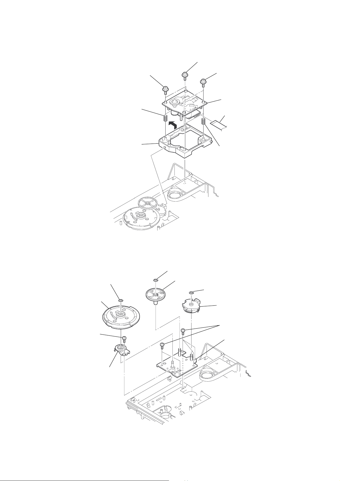
NOTE FOR MAIN GEAR INSTALLATION
5
Stopper washer (5)
4
Install the MAIN GEAR
as show in the drawing.
A
3
Rotate the GEAR (U/D)
to the arrow
A
direction.
B
2
Slide the SET LEVER to the
arrow
B
direction.
— 4 —
1
Set the mark of
ROTARY ENCODER.
Identifying the Parts
Front Panel
1
234
5
6
7
SECTION 1
GENERAL
8
90
@¡@¢
!¡
!ª
!£
!™ !¢
!¶
@£@∞
1 POWER switch
2 CONTINUE button
3 SHUFFLE button
4 PROGRAM button
5 REPEAT button
6 DISC CHECK button: CE215/CE315 model
TIME button: C160Z/C260Z model
7 DISC 1-5 button
8 Display window
9 ” (play) button
!º P (pause) button
!¡ p (stop) button
!™ EX-CHANGE button
@™
!£ DISC SKIP button
!¢ 6 OPEN/CLOSE button
!∞ AMS knob
!§ FADER button
!¶ MUSIC SCAN button
!• CLEAR button
!ª CHECK button
@º ) (forward) button
@¡ 0 (backward) button
@™ Disc tray
@£ PEAK SEARCH button: CE215/CE315 model
@¢ EDIT/TIME FADE button: CE215/CE315 model
@∞ TIME button: CE215/CE315 model
@º !•
!§
!∞
— 5 —
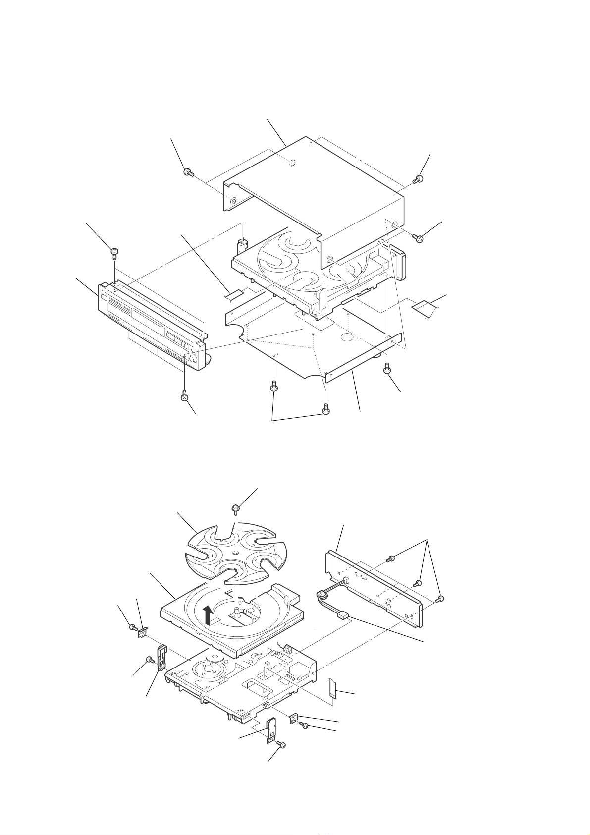
SECTION 2
DISASSEMBLY
Note : Follow the disassembly procedure in the numerical order given.
2-1. CASE, BOTTOM PLATE AND FRONT PANEL
4
Case
1
Two screws
(M3
×
8)
!º
Two screws
(BVTT3
!™
Front panel
×
8)
9
Flat type wire (9 core)
(MAIN board, to CN402)
3
Two screws
(BV3
×
8)
2
Two screws
(M3
8
Flat type wire (35 core)
(MAIN board, to CN402)
×
8)
!¡
Three screws
(BVTP3
2-2. BACK PANEL AND DISC TABLE
!¢
Disc table (B)
!∞
Disc table (A)
!™
Bracket
9
Screw
(BVTP3
(guideB1)
×
8)
×
8)
0
Bracket (guide F1)
!¡
Screw
(BVTP3
×
10)
5
Four screws
(BVTP3
!£
Screw
(PTPWH3
×
10)
×
12)
7
Bottom plate
3
Back panel
4
6
Three screws
(BVTP3
Flat type wire (6 core)
(MAIN board, to CN404)
×
10)
2
Five screws
(BVTP3
1
Connector
×
10)
8
Bracket (guide F1)
7
Screw (BVTP3 × 8)
— 6 —
6
Bracket (guide B1)
5
Screw
(BVTP3
×
8)
2-3. OPTICAL PICK-UP BLOCK ASSEMBLY
3
Two screws
(PTPWH2.6
6
Compression spring (BU)
5
Holder (BU)
2
Screw
(PTPWH3
×
6)
×
12)
4
Two screws
(PTPWH2.6
8
Optical pick-up block assembly
1
Flat type wire (16 core)
(BD board, to CN101)
7
Compression spring (BU)
×
6)
2-4. BRACKET (GEAR) ASSEMBLY
3
Stopper washer (5)
4
Gear (MAIN)
5
Screw
(BVTP3
×
8)
6
Rotary encoder
1
Stopper washer (5)
2
Gear (REV)
7
Stopper washer (5)
8
Gear (U/D)
9
Five screws
(BVTP3
0
Bracket (GEAR)
assembly
×
8)
Note : As for the installation of the main gear, refer to “Note for MAIN
GEAR installation” on page 4.
— 7 —
SECTION 3
ELECTRICAL BLOCK CHECKING
Note :
1. CD Block is basically designed to operate without adjustment.
Therefore, check each item in order given.
2. Use YEDS-18 disc (3-702-101-01) unless otherwise indicated.
3. Use an oscilloscope with more than 10MΩ impedance.
4. Clean the object lens using an applicator with neutral detergent
when the signal level is low than specified value with the
following checks.
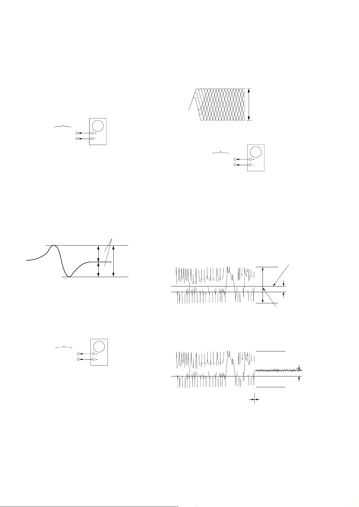
S Curve Check
oscilloscope
BD board
TP (FE)
TP (VC)
Procedure :
1. Connect oscilloscope to test point TP (FE) on BD board.
2. Connect between test point TP (FEI) and TP (VC) by lead wire.
3. Turn Power switch on.
4. Put disc (YEDS-18) in and turn Power switch on again and
actuate the focus search. (Actuate the focus search when disc
table is moving in and out.)
5. Check if the oscilloscope waveform (S-curve) is symmetrical
between A and B. And confirm peak to peak level within 3±1
Vp-p.
S-curve waveform
symmetry
Note :
A clear RF signal waveform means that the shape “ ◊ ” can
be clearly distinguished at the center of the waveform.
RF signal waveform
VOLT/DIV : 200mV
TIME/DIV : 500ns
level :
1.25 ± 0.25 Vp-p
E-F Balance Check
oscilloscope
BD board
TP (TE)
TP (VC)
Procedure :
1. Connect test point TP1 (ADJ) to ground with a lead wire.
2. Connect oscilloscope to test point TP (TE) on BD board.
3. Turned Power switch on.
4. Put disc (YEDS-18) in to play the number five track.
5. Press the “3” button. (The tracking serv o and the sledding servo
are turned OFF.)
6. Check the level B of the oscilloscope's waveform and the A
(DC voltage) of the center of the Traverse waveform.
Confirm the following :
A/B × 100 = less than ± 22%
A
within 3 ± 1 Vp-p
B
6. After check, remove the lead wire connected in step 2.
Note : • Try to measure several times to make sure than the ratio
of A : B or B : A is more than 10 : 7.
• Take sweep time as long as possible and light up the
brightness to obtain best waveform.
RF Level Check
oscilloscope
BD board
TP (RF)
TP (VC)
Procedure :
1. Connect oscilloscope to test point TP (RF) on BD board.
2. Turned Power switch on.
3. Put disc (YEDS-18) in to play the number five track.
4. Confirm that oscilloscope waveform is clear and check if RF
signal level is correct or not.
Traverse waveform
Center of the waveform
B
0V
level : 1.3 ± 0.6 Vp-p
A (DC voltage)
7. Press the “8” button. (The tracking servo and sledding servo
are turned ON.) Confirm the C (DC voltage) is almost equal to
the A (DC voltage) is step 6.
Traverse waveform
0V
Tracking servo
Sledding servo
OFF
Tracking servo
Sledding servo
ON
8. Disconnect the lead wire of TP (ADJ) connected in step 1.
C (DC
voltage)
— 8 —
RF PLL Free-run Frequency Check
Procedure :
1. Connect frequency counter to test point (PLCK) with lead wire.
BD board
TP (PLCK)
2. Turned Power switch on.
3. Put the disc (YEDS-18) in to play the number five track.
Confirm that reading on frequency counter is 4.3218MHz.
frequency counter
Adjustment Location :
[ BD BOARD ] — Conductor Side —
1
20
(FE)
(FEI)
(RF)
IC103
11
10
(PLCK)
IC101
(TE)
(VC)
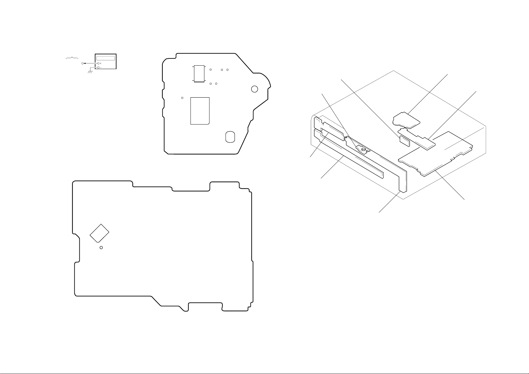
4-1. CIRCUIT BOARDS LOCATION
TABLE MOTOR BOARD
LOADING MOTOR BOARD
CDP-C160Z/C260Z/CE215/CE315
SECTION 4
DIAGRAMS
BD BOARD
SENSOR BOARD
[ MAIN BOARD ] — Conductor Side —
40
41
IC302
80
1
TP1
(ADJ)
25
24
64
65
POWER SW BOARD
KEY BOARD
MAIN BOARD
DISPLAY BOARD
— 9 — — 10 —
 Loading...