

Sony ACX709AKN Datasheet

7.60cm Reflective Color LCD Module
Description
The ACX709AKN is a 7.60cm diagonal, 320 × 320
dots (102,400 effective pixels) active matrix reflective
color TFT-LCD module with a high performance front
light unit with touch panel. This panel provides ultrahigh reflection ratio with high contrast ratio. These
characteristics are realized by a newly developed
reflective electrode structure.
Features
• Number of effective dots: 320 × 320
• Pixel pitch: 168µm × 168µm
• High reflection ratio
• High contrast ratio
• Number of colors: 262,144
• Compact size
• Thin and bright front light unit with touch panel
ACX709AKN
Element Structure
• Number of dots
Number of active dots: 320 (H) × 320 (V) × 102,400
• Dimensions
Module dimensions: 64.65mm (W) × 87.65mm (D) × 6.0mm (H) (excluding FPC and area)
Effective display dimensions: 53.76mm (H) × 53.76mm (V)
Applications
PDA, etc.
Sony reserves the right to change products and specifications without prior notice. This information does not convey any license by
any implication or otherwise under any patents or other right. Application circuits shown, if any, are typical examples illustrating the
operation of the devices. Sony cannot assume responsibility for any problems arising out of the use of these circuits.
– 1 –
E01416A15-PS
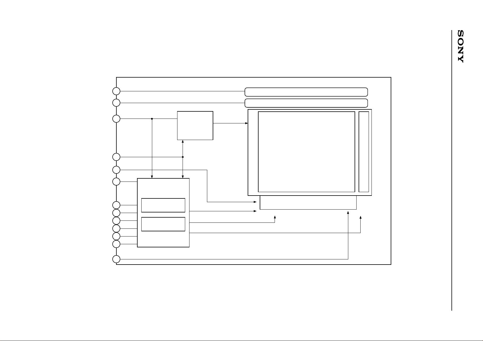
Block Diagram
The block diagram of this LCD module is shown below.
– 2 –
T1, T2
T3, T4
LED
V
CC
(+3.0V)
ENV
EE
Data in
(RGB × 6-bit)
DD
(+5.0V)
V
FHSYNC
FVSYNC
FSCLK
PWM1
FMOD
FLCLK
TG
LCD Controller
Reference
Voltage Driver
DC-DC
Converter
Control Pulse
Vref
VCOM
+9.0V
–3.0V
–6.5V
Touch Panel
Front Light (LED)
Poly-Si TFT LCD
(320 × RGB × 320)
H Driver (TAB-IC)
V Driver
+5.0V
FDE
ACX709AKN
Absolute Maximum Ratings (Ta = 25°C, VSS = 0V)
• Supply voltage VDD –0.3 to +6.0 V
VCC –0.3 to +4.6 V
• Input voltage VI –0.3 to VDD/VCC + 0.3 V
• Storage temperature Tstg –20 to +60 °C
• LED current Iled (as below) mA
30
25
20
10
Iled [mA]
0
Allowable LED current
0
20 40
Ambient temperature Ta [˚C]
60 80 100
Recommended Operating Conditions
• Supply voltage VDD 4.7 to 5.3 V
VCC 2.7 to 3.3 V
• Operating temperature Topr 0 to +50 °C
ACX709AKN
Pin Description
Pin No. Symbol Description
1
2
3
4
5
6
7
8
9
10
11
12
13
14
15
VDD
VDD
VDD
GND
PWM1
ENVEE
FMOD
PWM0
FLCLK
FHSYNC
FVSYNC
GND
FSCLK
GND
GND
Power supply (+5V)
Power supply (+5V)
Power supply (+5V)
Vertical sampling clock
Power control pulse
Common plane pulse
Data enable pulse
Horizontal control pulse
Start signal of horizontal timing
Start signal of vertical timing
Data sampling clock
Pin No.
21
22
23
24
25
26
27
28
29
30
31
32
33
34
35
Symbol
Data30
GND
Data25
Data24
Data23
Data22
Data21
Data20
GND
Data15
Data14
Data13
Data12
Data11
Data10
Description
Data signal
Data signal
Data signal
Data signal
Data signal
Data signal
Data signal
Data signal
Data signal
Data signal
Data signal
Data signal
Data signal
16
17
18
19
20
Data35
Data34
Data33
Data32
Data31
Data signal
Data signal
Data signal
Data signal
Data signal
– 3 –
36
37
38
39
40
FDE
GND
VCC
VCC
VCC
Signal control pulse
Power supply (+3V)
Power supply (+3V)
Power supply (+3V)
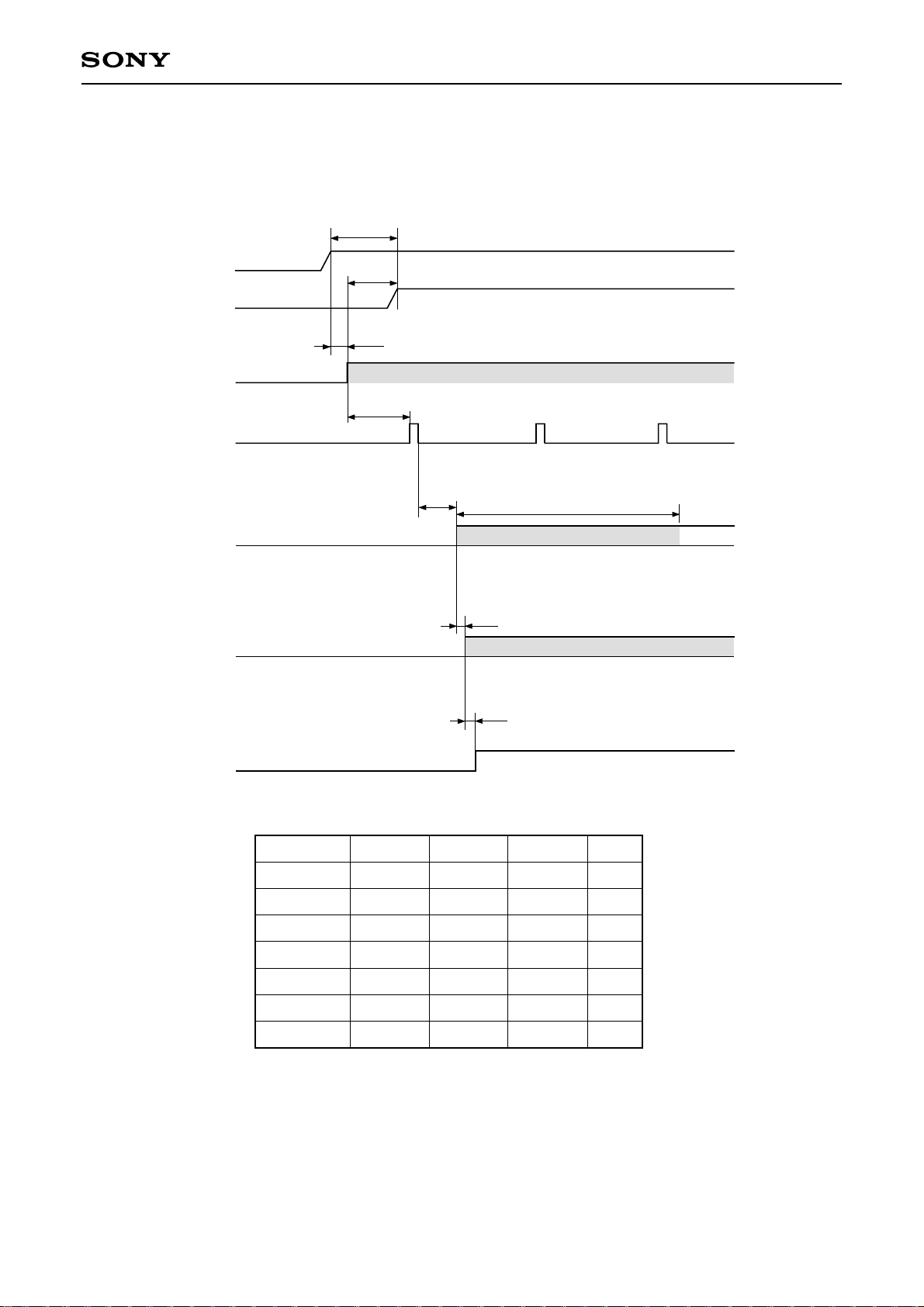
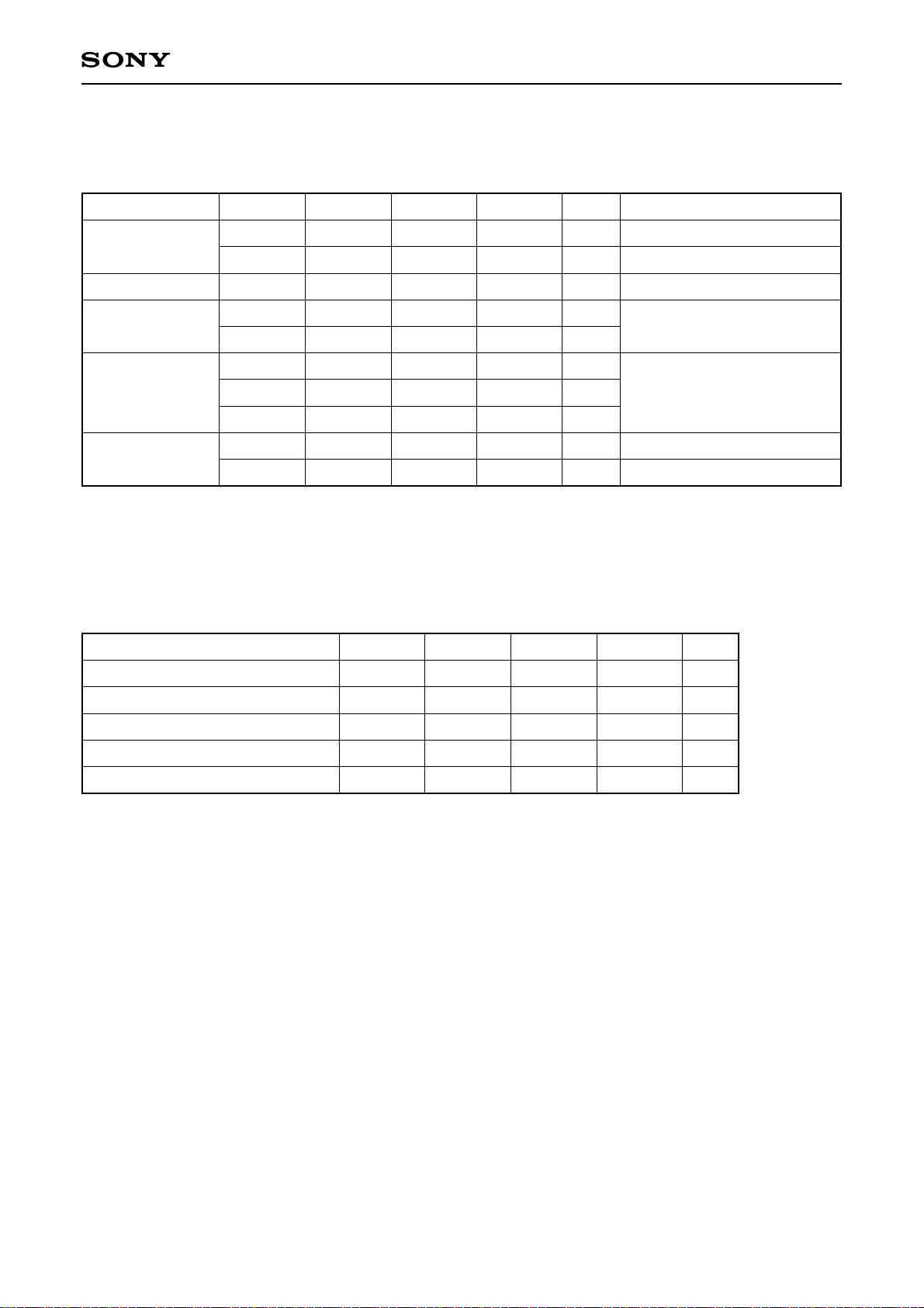
Power Sequence
(1) Power-up Sequence
3.0V
5.0V
Pulses
(except FVSYNC,
Data, FMOD, ENVEE)
FVSYNC
Low
Low
within
10ms
t
pv2
t
pv1
t
pv3
ACX709AKN
3.0V
0
5.0V
0
active
t
pd
2 fields
DATA (out)
FMOD
ENV
EE
All data: White activeLow
t
df
Low
t
sp
Low
Item Min. Typ. Max. Unit
tpv1
tpv2
tpv1 + tpv2
tpv3
tpd
tdf
tsp
0
1
—
0
321PWM1
0
0
—
—
—
—
—
—
—
—
—
10
—
322PWM1
10
10
active
High
µs
ms
ms
µs
µs
µs
– 4 –
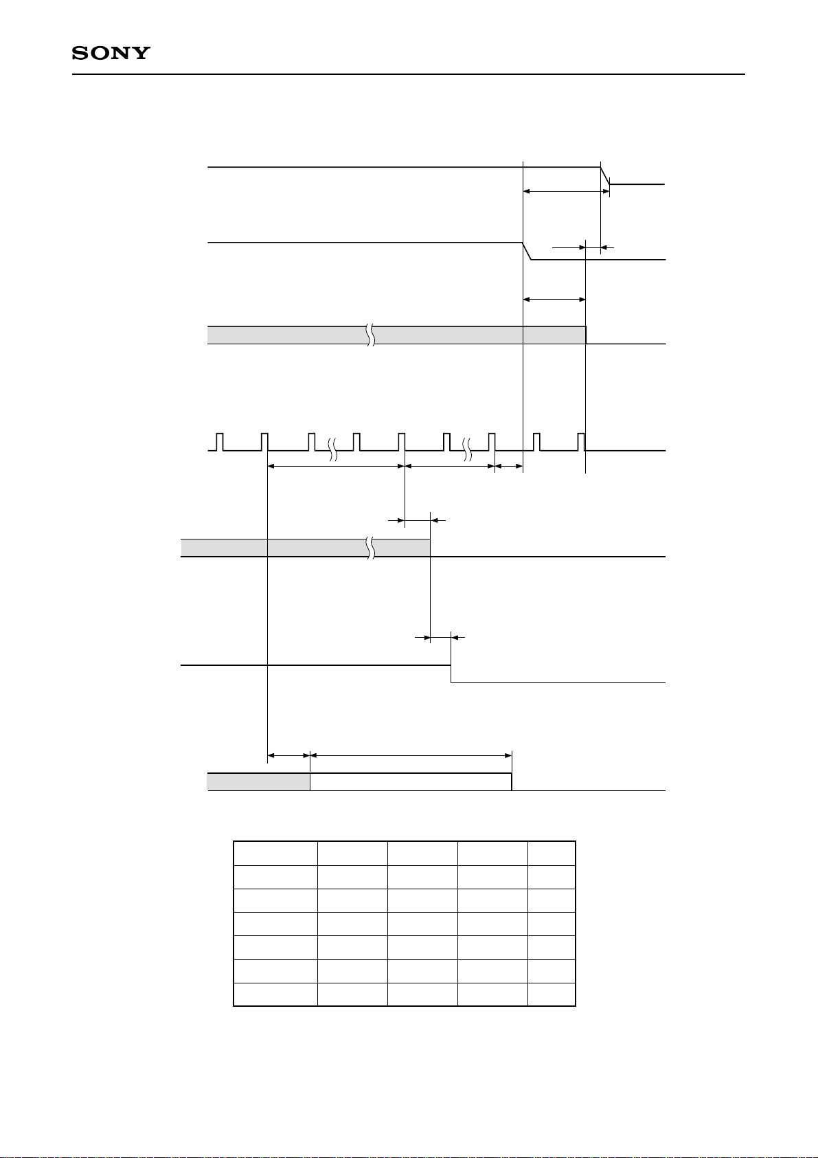
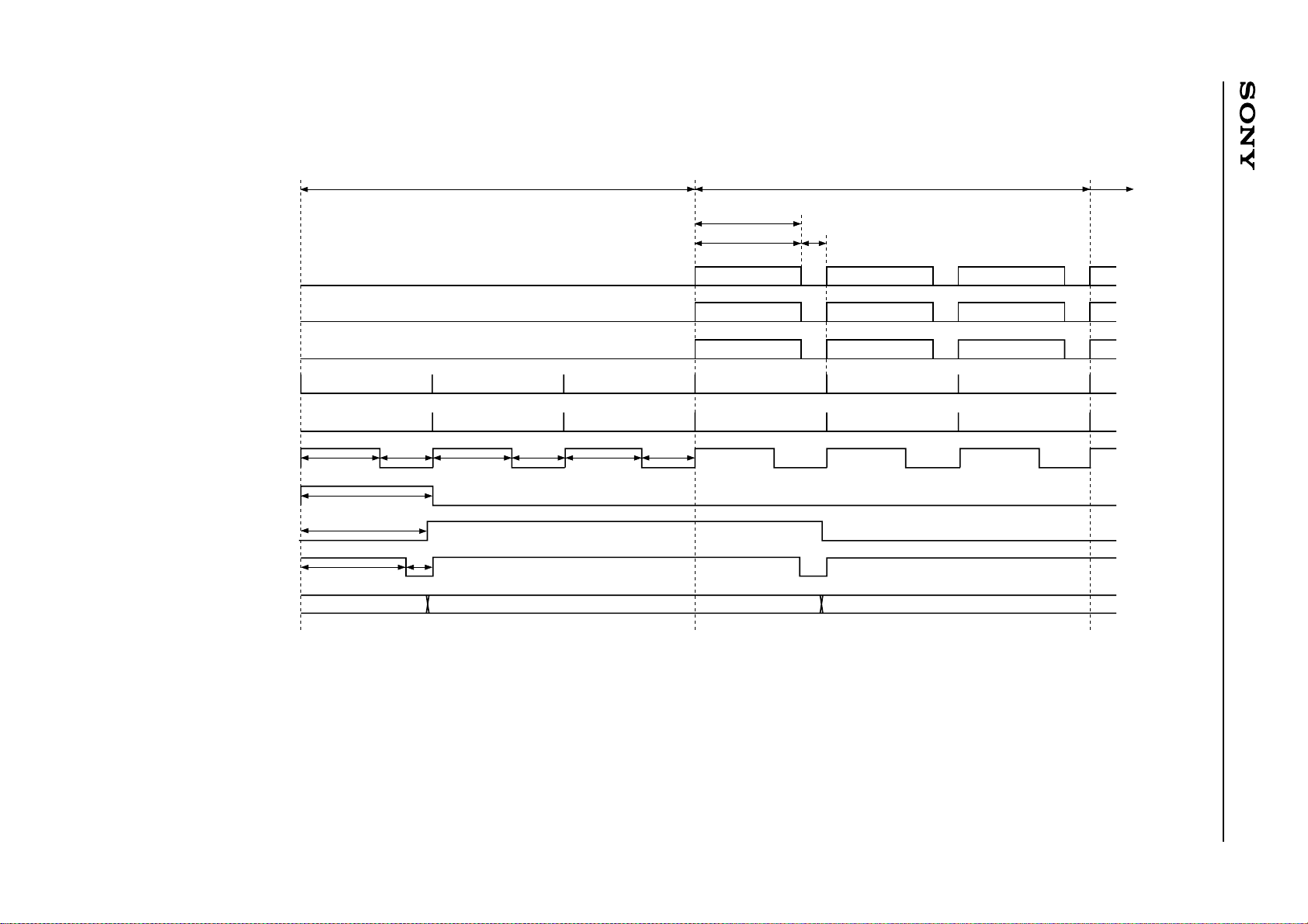
(2) Power-down Sequence
ACX709AKN
Pulses
(except FVSYNC,
Data, FMOD, ENV
FVSYNC
FMOD
3.0V
5.0V
EE
3.0V
within 10ms
t
pv1
t
pv2
)
active
active
t
df
t
vs10 fields (min.)5 fields (min.)
Low
Low
Low
(Low timing is the
same as "Pulse")
0
5.0V
0
3.0V
0
ENV
DATA
EE
t
fp
active
t
vdw 6 fields (min.)
active All data: White
Item Min. Typ. Max. Unit
tpv1
tpv2
tvs
tvdw
tdf
tfp
0
0
0
321PWM1
0
0
—
—
—
—
—
—
—
—
—
322PWM1
10
10
Low
Low
µs
µs
µs
µs
µs
– 5 –
Electrical Characteristics
(1) Voltage and Current Characteristics
ACX709AKN
Item
Symbol
VDD
Min. Typ. Max. Unit Pins
4.7
Supply voltage
VCC
Ripple voltage
Input
Vrip
VH1
VL1
Vt+
Input voltage 2
Vt–
Vt– – Vt+
Current
consumption
1
∗
VCC = 3.0V/VDD = 5.0V gray scale (16 steps)
2
∗
VCC = 3.3V/VDD = 3.8V black raster
IVDD
IVCC
2.7
—
0.7VCC
—
—
0.15VCC
0.2
—
—
(2) Timing
Item
Master clock (MCK)
DATA setup time
DATA hold time
Start pulse setup time
Start pulse hold time
Symbol
tclk
tSETUP1
tHOLD1
tSETUP2
tHOLD2
5.0
3.0
7.0
5.0
—
—
—
—
—
1
∗
1
∗
5.3
3.3
100
—
0.2VCC
0.75VCC
—
2
∗
8.0
2
∗
6.3
V
V
mV
V
V
V
V
V
mA
mA
VDD
VDD
FSCLK
(LVTTL level input)
All inputs except for MCK
(LVTTL level Schmitt trigger
input)
Min. Typ. Max. Unit
—
4
1
4
1
8.0
—
—
—
—
10
—
—
—
—
tclk
ns
ns
ns
ns
– 6 –
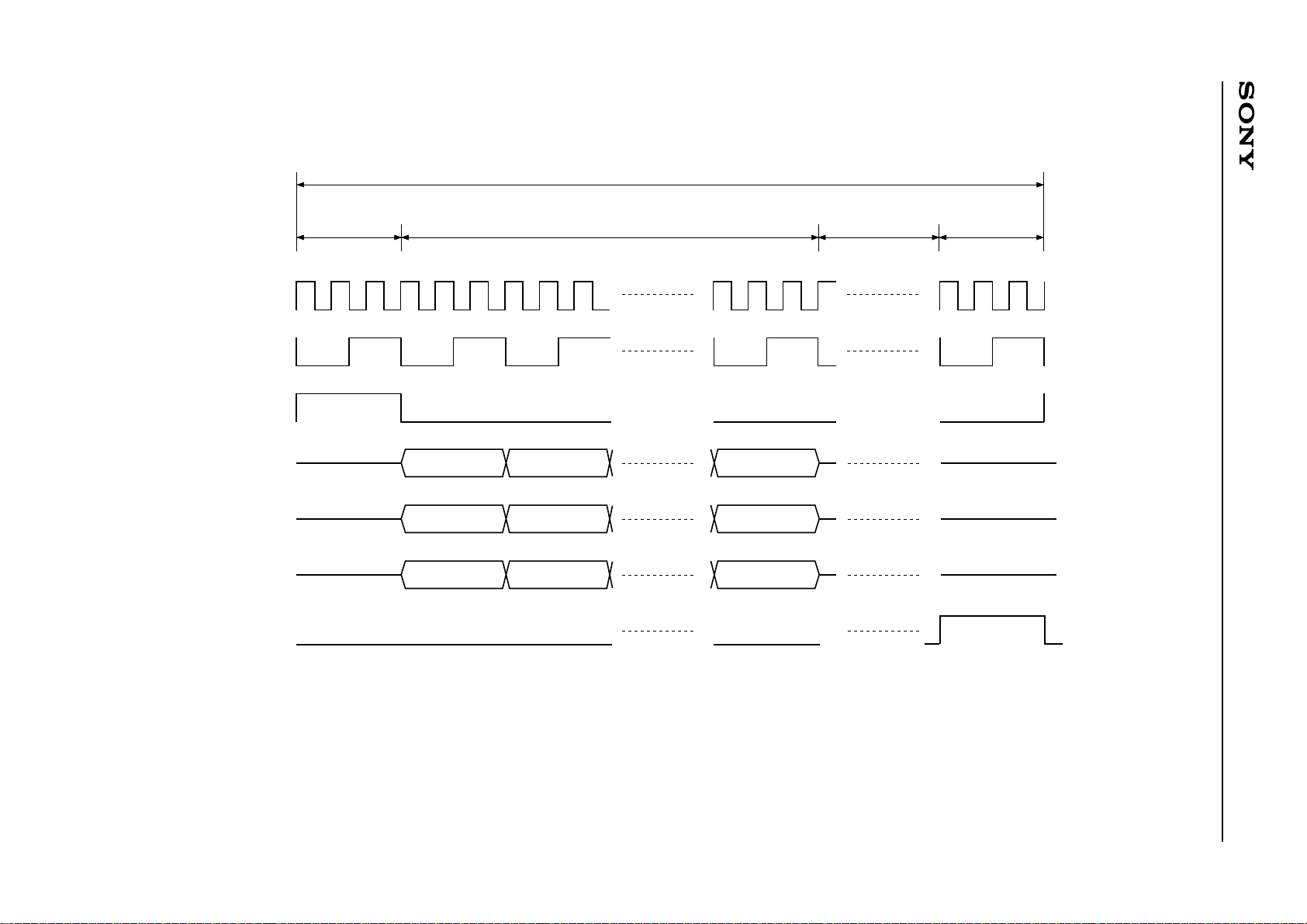
(3) Horizontal Timing Chart
420 FSCLK
First Display Line
108
107 32
Data10 to 15
Data20 to 25
Data30 to 35
B0, B3, B6,
B1, B4, B7,
B2, B5, B8,
...
, B318 G0, G3, G6,
...
, B319 G1, G4, G7,
...
, X G2, G5, G8,
...
, G318 R0, R3, R6,
...
, G319 R1, R4, R7,
...
, X R2, R5, R8,
...
, R318
...
, R319
...
, X
FDE
FHSYNC
– 7 –
FLCLK
FVSYNC
PWM1
PWM0
80
133
107
140
60
33
80
60
80
60
FMOD
ACX709AKN
(4) Detail of Horizontal Sequence (Example of B)
1 FSCLK 107 FSCLK 31 FSCLK 1 FSCLK
Pixel Clk
FSCLK
FDE
– 8 –
Data10
to
15
to
Data20
25
140 FSCLK
B0 B3 B318
B1 B4 B319
Data30
FHSYNC
to
35
B2 B5 X
ACX709AKN
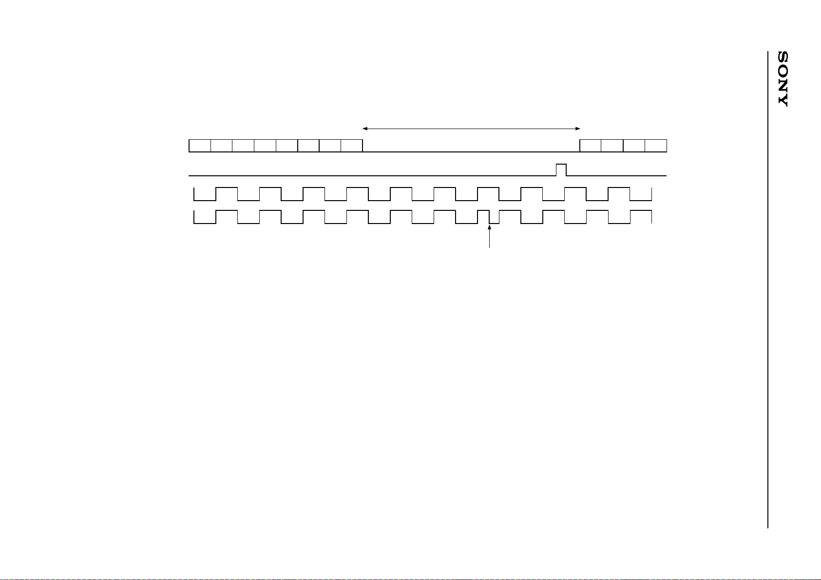
(5) Ve rtical Timing Chart
V Blanking
Display Data
FVSYNC
PWM1
FMOD
313 314 315 316 317 318 319 320
FMOD phase variation point
1 2 34
– 9 –
Notes) 1. Inversion pulse of PWM1 is not mentioned.
2. The pulse of FMOD is not prescribed.
ACX709AKN
 Loading...