

Sony ACX705AKM Datasheet
ACX705AKM
6.92cm Diagonal Reflective Color LCD Module
Description
The ACX705AKM is a 6.92cm diagonal active
matrix reflective color TFT-LCD module with a front
light unit and a driving board. This module provides
low power consumption which is realized by built-in
3-bit digital interface circuitry.
Features
• Number of dots: 240 × RGB × 160
• Dot size: 80µm × 240µm
• High reflectivity: (25% typ.)
• High contrast ratio: (13:1 typ. at the condition of turning off the front light)
• Number of colors: 512
• Low power consumption (47mW typ.) with a driving board composed of a LCD controller IC,
a reference driver IC and a DC-DC convertor
• Built-in 3-bit digital interface circuitry
• Compact size
• Thin and bright front light unit
Element Structure
• Active matrix TFT-LCD panel with built-in peripheral driving circuitry using low temperature polycrystalline
silicon transistors
• Number of dots
Total number of dots: 242 × 3 (H) × 162 (V) = 117,612
Number of active dots: 240 × 3 (H) × 160 (V) = 115,200
• Dimensions
Module dimensions: 71.4mm × 52.0mm × 4.8mm (t) (parts area 6.5mm (t) max.)
Effective display dimensions: 57.6mm (H) × 38.4mm (V)
Applications
PDA, etc.
– 1 –
E00847-PS
Sony reserves the right to change products and specifications without prior notice. This information does not convey any license by
any implication or otherwise under any patents or other right. Application circuits shown, if any, are typical examples illustrating the
operation of the devices. Sony cannot assume responsibility for any problems arising out of the use of these circuits.
– 2 –
ACX705AKM
Absolute Maximum Ratings (Ta = 25°C, VSS = 0V)
• Supply voltage VCC1VSS – 0.3 to +5.5 V
VCC2VSS – 0.3 to +5.5 V
• Input voltage VI VSS – 0.3 to VCC2 + 0.3 V
• Storage temperature Tstg –30 to +70 °C
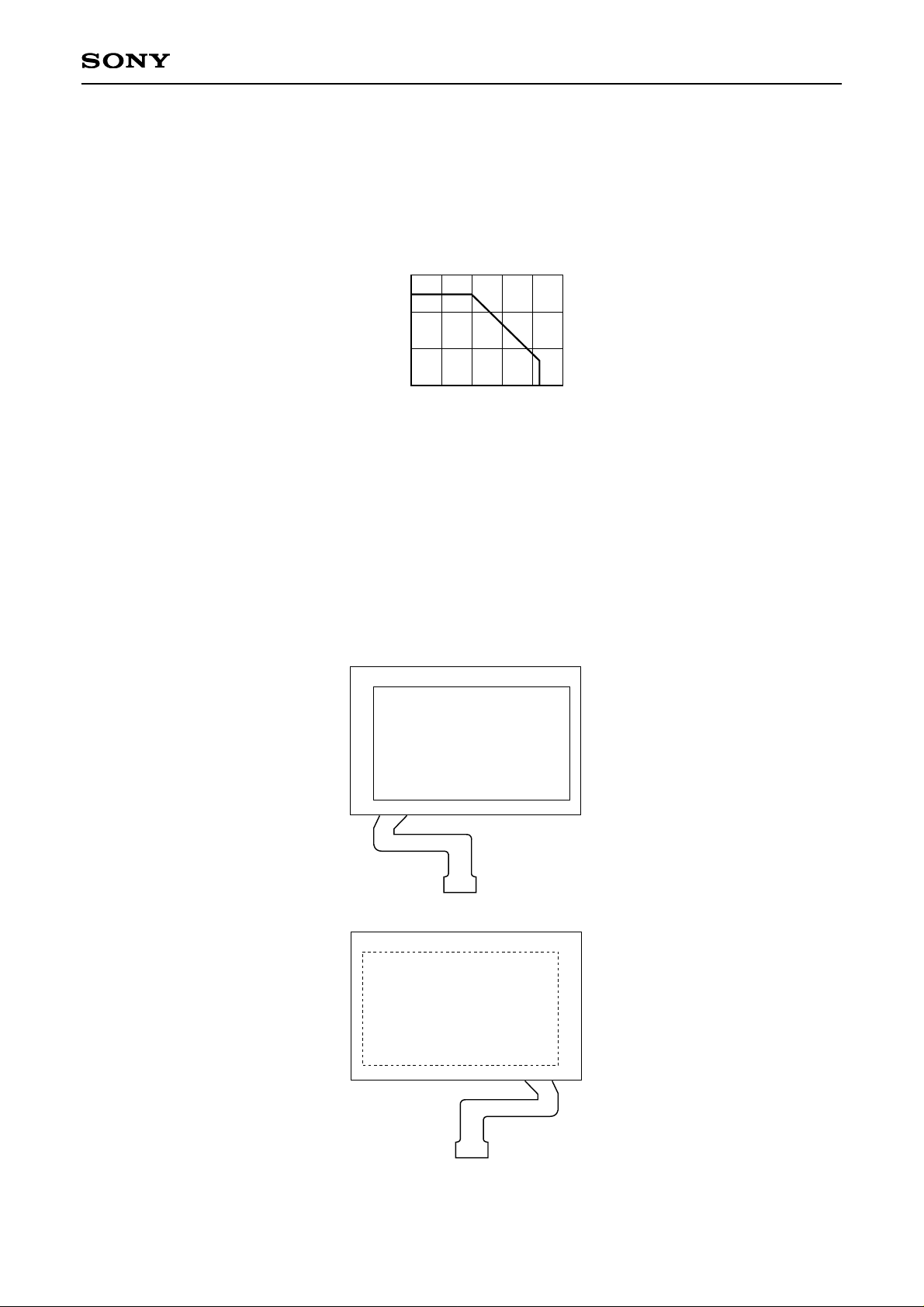
• LED current Iled (as below)
Right
Left Active area
Top
Bottom
Left Right
Top
Front View
Rear View
Bottom
Pin 22Pin 1
0
0
10
20
Allowable forward current
Iled [mA]
30
25
20 40
Ta [°C]
60 80 100
Recommended Operating Conditions
• Supply voltage VCC1 3.50 to 4.20 V
VCC2 2.55 to 3.15 V
• Operating temperature Topr –10 to +60 °C
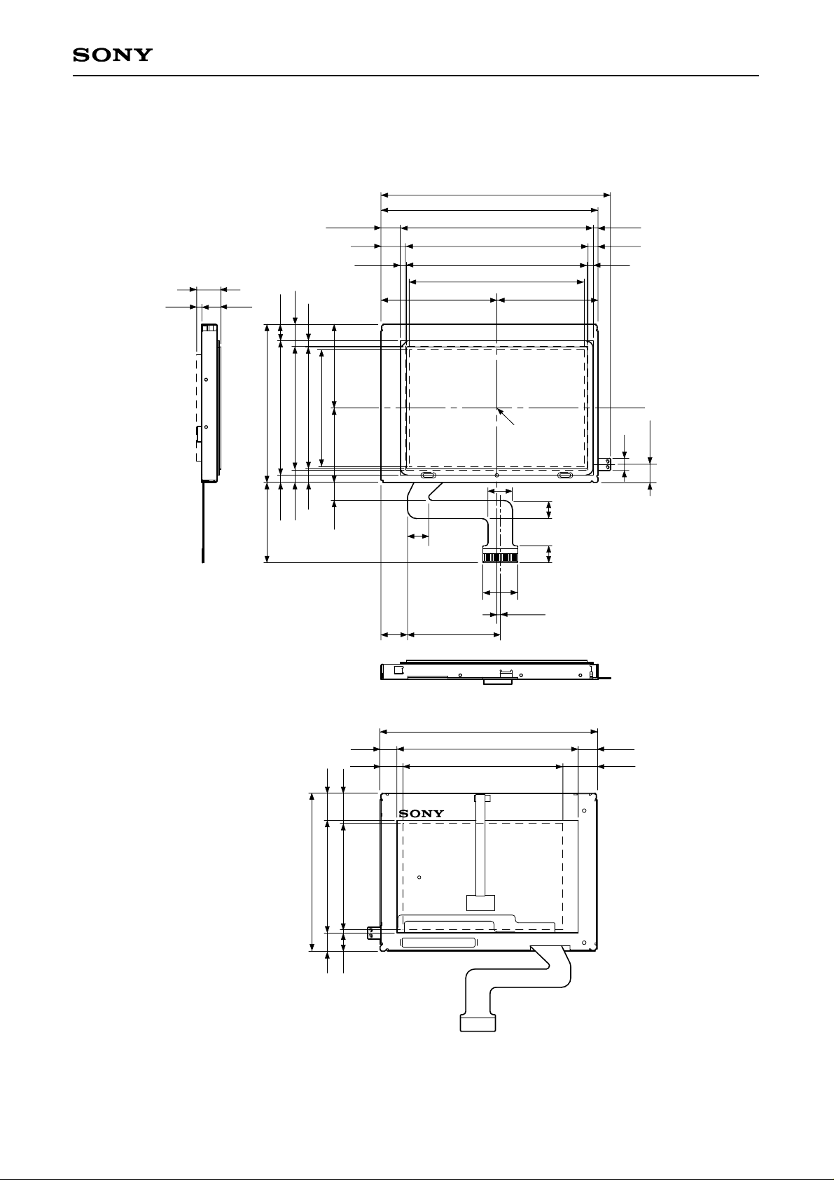
Pin Location of Panel Block
The FPC pin assignment is described in on page 5. The location of Pin 1 is shown below.
– 3 –
ACX705AKM
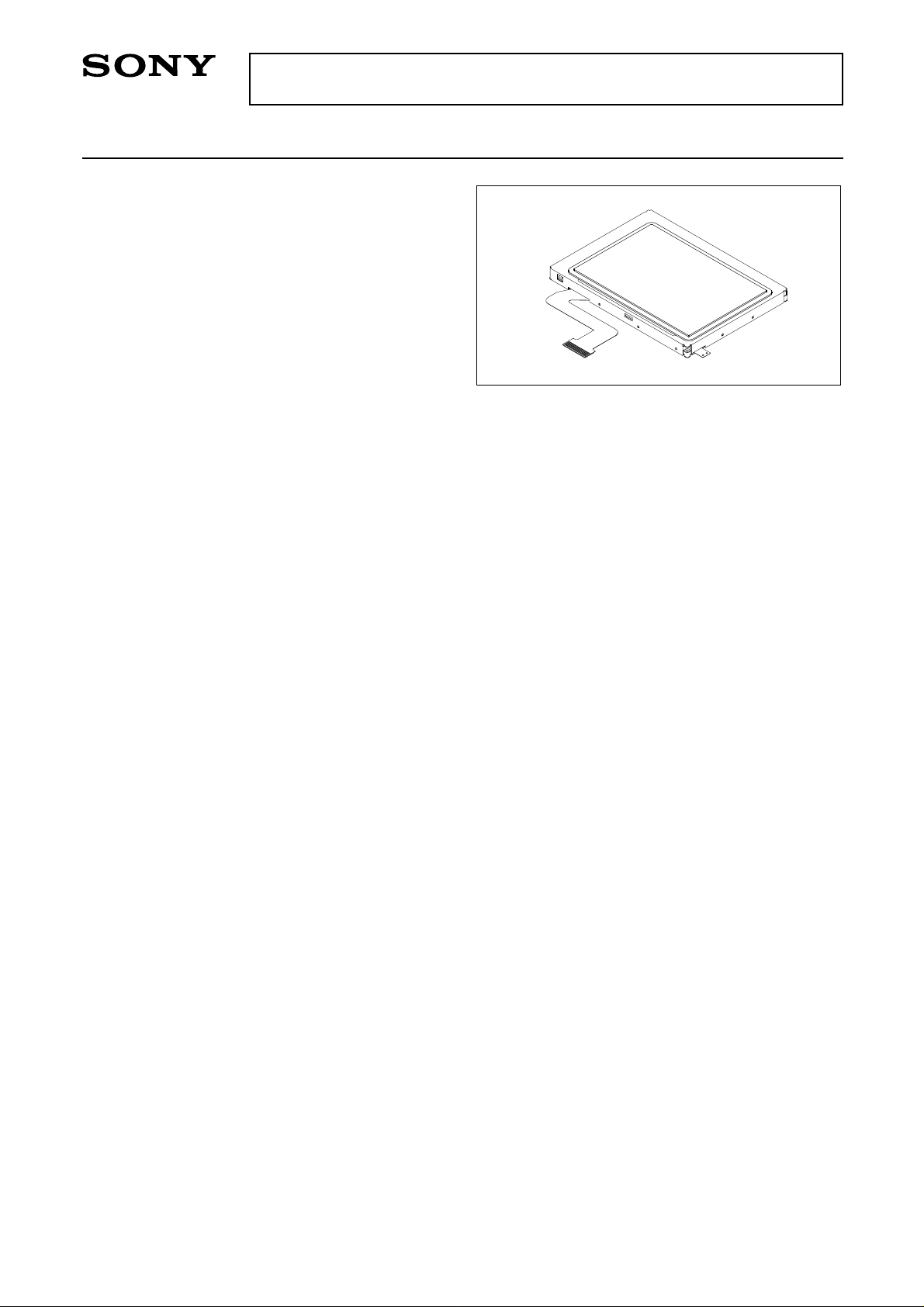
Module Configuration
This module is composed of a reflective color TFT-LCD panel, a front light unit and a driving board as shown in
the figure below.
Rear View
Front View
Active area
center
ACX705AKM-7 T
ACX705AKM-01
71.4 (Outer frame)
8.1
[(75.5)]
57.6 (Active area)
(33.3)
60
+0.1
0
(Window)
(3.3)
38.1
(5.93)
(8.75)
30.5
(1.15)
4
8
7
11.5
6
5.5
(5.1)
(1.7)
(7.6)
52.6
0
–0.1
(Parts area)
(11.3)
(7.5)
59.6
+0.1
0
(Window)
(6.3)
(5.5)
71.4 ± 0.3 (Outer frame)
(59.4)
(2)
6.4 ± 0.3
63.4 (Cover plate)
(1.6)
(2)
(7)
52 ± 0.3 (Outer frame)
(6)
(9)
37
+0.1
0
(Window)
35
0
–0.1
(Parts area)
(10)
(4.08)
(40.2)
38.4 (Active area)
(24.48)
27.52
52 ± 0.3
7.12
40.8
+0.1
0
(Window)
(5.9)
(26.4)
2
5.42
44.2 (Cover plate)
(2.38)
(2)
– 4 –
ACX705AKM
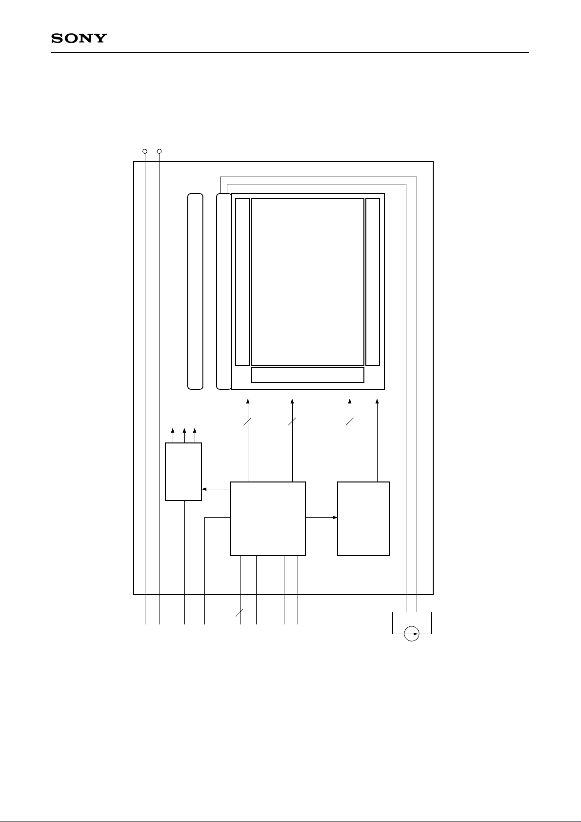
Block Diagram
The block diagram of this LCD module is shown below.
+9.0V
+5.0V
–6.5V
Control pulse
Control pulse
Control pulse
+5.0V
+3.0V
Vref
VCOM
36
Data
RGB × 3-bit × 4
9
22
8
+9.0V, –6.5V
15mA
(25°C)
Cover Plate
Front Light (LED)
H Driver
V Driver
H Driver
Poly-Si TFT LCD
(240 × RGB × 160)
CXD3507GG
(LCD Controller)
DC-DC
Converter
CXD2475TQ
(Reference
Voltage Driver)
MIC1
MIC2
Vcc1 (+3.8V)
Vcc2 (+3.0V)
Data in
(RGB × 3-bit)
Hsync
Vsync
MCK
S/D
– 5 –
ACX705AKM
Pin Description
Pin No. Symbol Description
1
2
3
4
5
6
7
8
9
10
11
12
13
14
15
16
17
18
19
20
21
22
MIC1
MIC2
V
CC1
VCC1
GND
GND
R0
R1
R2
G0
G1
G2
B0
B1
B2
Hsync
Vsync
S/D
MCK
V
CC2
LED VDD
LED GND
+3.8V power supply
+3.8V power supply
Ground
Ground
Red data input (LSB)
Red data input
Red data input (MSB)
Green data input (LSB)
Green data input
Green data input (MSB)
Blue data input (LSB)
Blue data input
Blue data input (MSB)
Hsync input
Vsync input
Shut down
Master clock (4.2MHz)
+3.0V power supply
LED VDD
LED GND
– 6 –
ACX705AKM
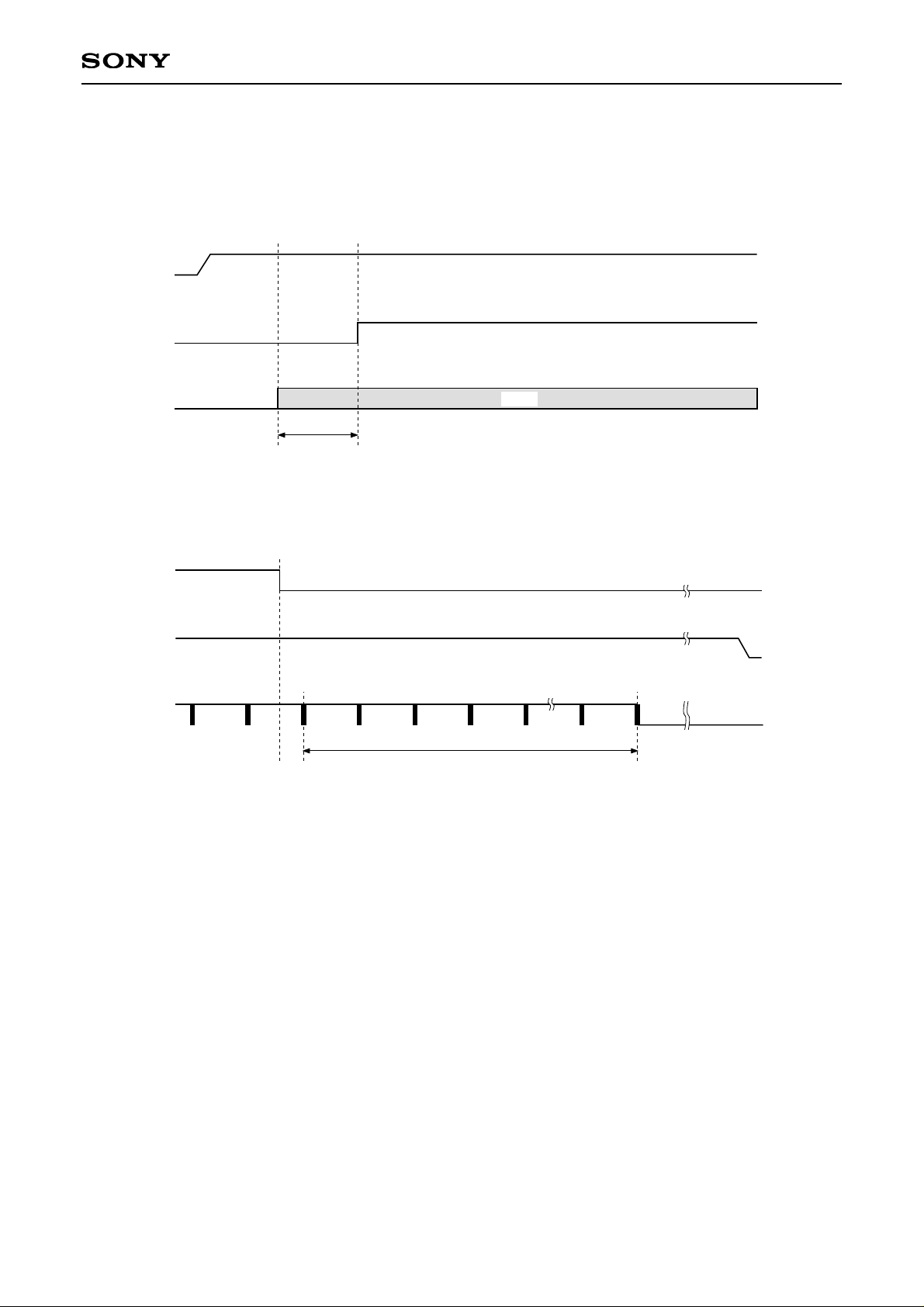
S/D
There are input for power up/down sequence.
Power Up Sequence
S/D Inactive (low)
Vcc2
0
Active
MCK
Hsync
Vsync
DATA (in)
Invalid (low)
Vcc2
0
Vcc1, Vcc2
Vcc1, Vcc2
0
1 Field (typ.)
Valid
Vcc1, Vcc2
Active
Vcc1, Vcc2
0
In active (low)
Vsync
Vcc2
0
S/D
Vcc2
0
13 Fields
Power Down Sequence
 Loading...