

Sony ACX704AKM Datasheet
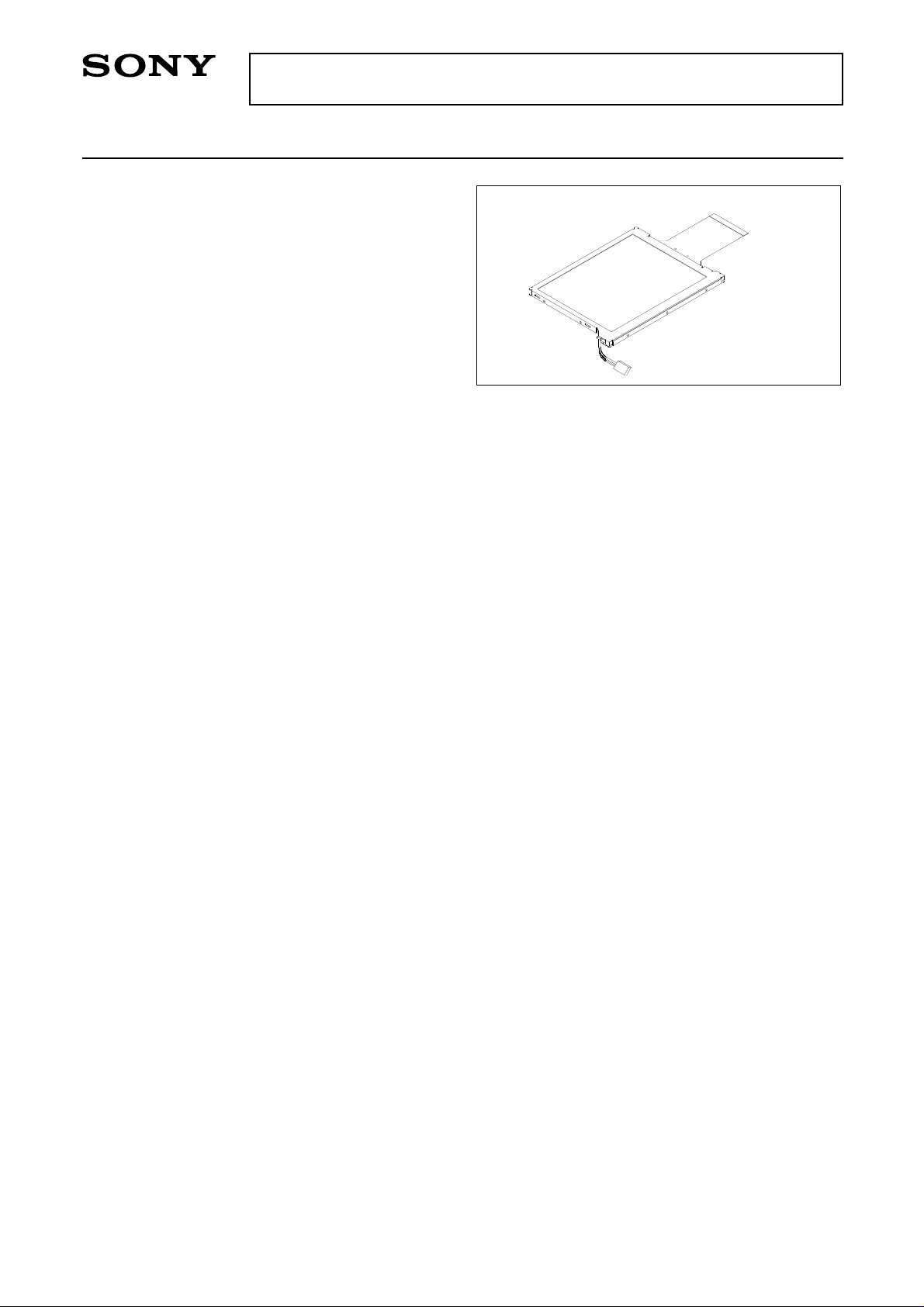
ACX704AKM
9.60cm (3.78 Type) QVGA Reflective Color LCD Module
Description
The ACX704AKM is a 9.60cm diagonal, QVGA
formatted active matrix reflective color TFT-LCD with
a high performance front light unit. This panel
provides ultra-high reflectivity (30% typ.) with high
contrast ratio (25:1 typ.). These characteristics are
realized by a newly developed reflective electrode
structure. In addition, this panel provides low power
consumption (20mW typ.) which is realized by builtin 4-bit digital interface circuitry addressed by low
temperature polycrystalline silicon transistors.
Features
• Number of dots: 320 × RGB × 240
• Dot size: 80µm × 240µm
• High reflectivity: 30% (typ.)
• High contrast ratio: 25:1 (typ.)
• Number of colors: 4096
• Low power consumption: 20mW (typ.)
• Built-in 4-bit digital interface circuitry
• Compact size
• Thin and bright front light unit
Element Structure
• Active matrix TFT-LCD panel with built-in peripheral driving circuitry using low temperature polycrystalline
silicon transistors
• Number of dots
Total number of dots: 322 × 3 (H) × 242 (V) = 233,772
Number of active dots: 320 × 3 (H) × 240 (V) = 230,400
• Dimensions
Module dimensions: 96.8 (W) × 73.0 (D) × 3.96 (H) (mm)
Effective display dimensions: 76.800 (H) × 57.600 (V) (mm)
Applications
PDA, etc.
– 1 –
E00813
Sony reserves the right to change products and specifications without prior notice. This information does not convey any license by
any implication or otherwise under any patents or other right. Application circuits shown, if any, are typical examples illustrating the
operation of the devices. Sony cannot assume responsibility for any problems arising out of the use of these circuits.
– 2 –
ACX704AKM
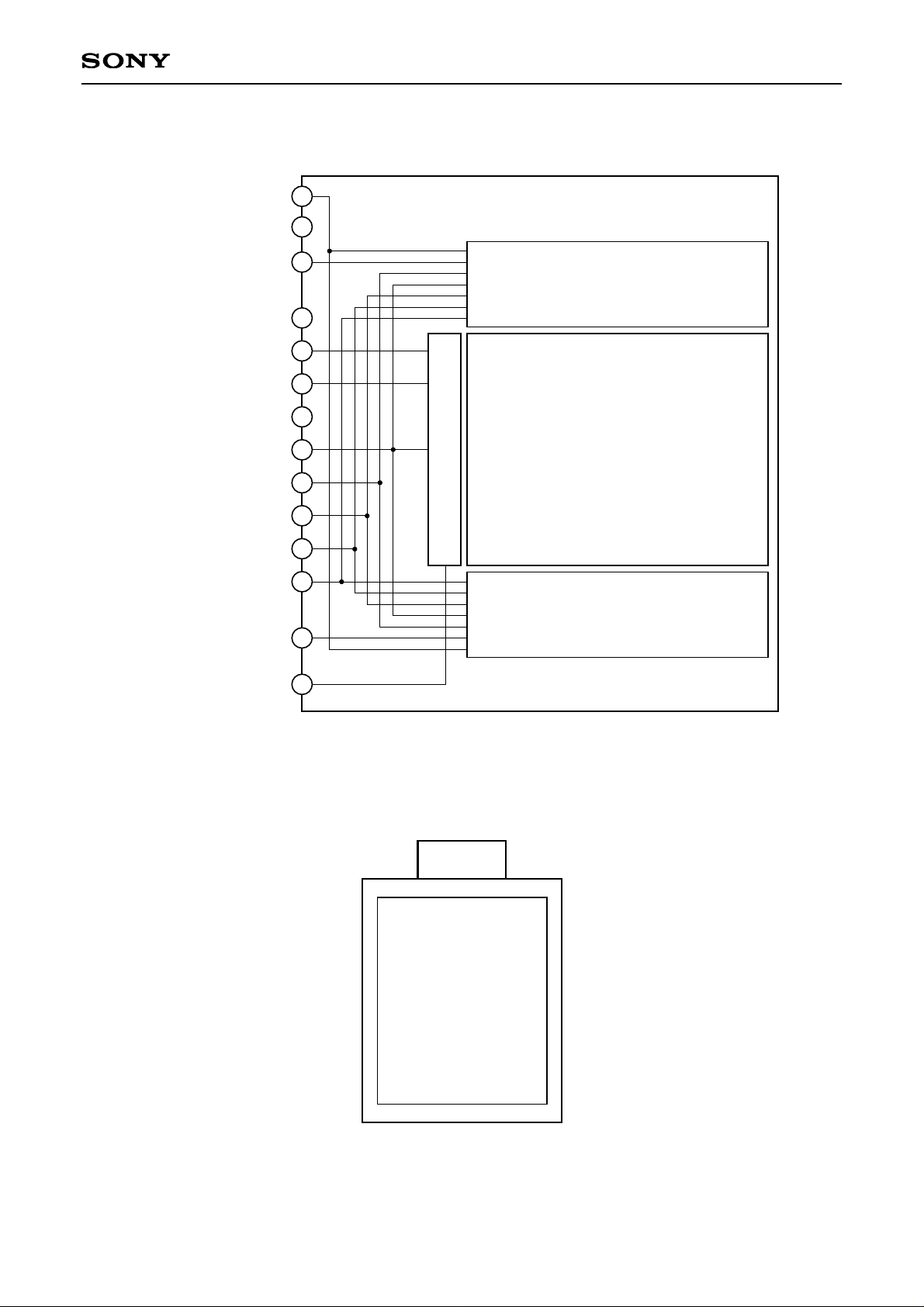
Block Diagram
The panel block diagram is shown below.
TEST4, TEST5
TEST3
R01 to 31, XR01 to 31,
G01 to 31, XG01 to 31,
B01 to 31, XB01 to 31
VCOM
VVDD, VVSS1, VVSS2
VST, XVST, ENB, XENB,
VCK, XVCK
TEST1, TEST2
RESET
HVDD, HVSS1, HVSS2
HCK1, XHCK1, HCK2, XHCK2,
HST1, XHST1, HST2, XHST2
OE1, XOE1, OE2, XOE2
V1, V2, V3, V4, V5, V6, V7, V8
R02 to 32, XR02 to 32,
G02 to 32, XG02 to 32,
B02 to 32, XB02 to 32
TEST6, TEST7
Horizontal Driver with Level Shifters
Vertical Driver with Level Shifters
Horizontal Driver with Level Shifters
Display Area
320 × RGB × 240
FPC
Pin 90 Pin 1
Active Area
Front View
Pin Location of Panel Block
The FPC pin assignment is described in the page 4. The location of Pin 1 is shown below.

– 3 –
ACX704AKM
Absolute Maximum Ratings (HVSS1, VVSS1 = 0V)
• H driver supply voltage 1 HVDD –1.0 to +10.5 V
• V driver supply voltage 1 VVDD –1.0 to +10.5 V
• H driver supply voltage 2 HVSS2 –7.5 to +1.0 V
• V driver supply voltage 2 VVSS2 –7.5 to +1.0 V
• Power-on reset input pin voltage RESET –1.0 to +10.5 V
• Vcom input pin voltage VCOM –1.0 to +10.5 V
• Reference voltage input pin voltage V0, V1, V2, V3, V4, V5, V6, V7, V8 –1.0 to +10.5 V
• H driver pulse input pin voltage HST1, XHST1, HST2, XHST2, HCK1, –1.0 to +10.5 V
XHCK1, HCK2, XHCK2, OE1, XOE1,
OE2, XOE2, TEST4, TEST5
• V driver pulse input pin voltage VST, XVST, VCK, XVCK, ENB, XENB, –1.0 to +10.5 V
TEST6, TEST7
• Data signal input pin voltage Rnm, XRnm, Gnm, XGnm, Bnm, XBnm –1.0 to +10.5 V
(n = 0, 1, 2, 3, m = 1, 2)
• Operating temperature Topr –10 to +40 °C
• Storage temperature Tstg –30 to +60 °C
Power Consumption
Less than 35mW (typ. 20mW) excluding the front light and supporting circuitry on the typical operating condition.
– 4 –
ACX704AKM
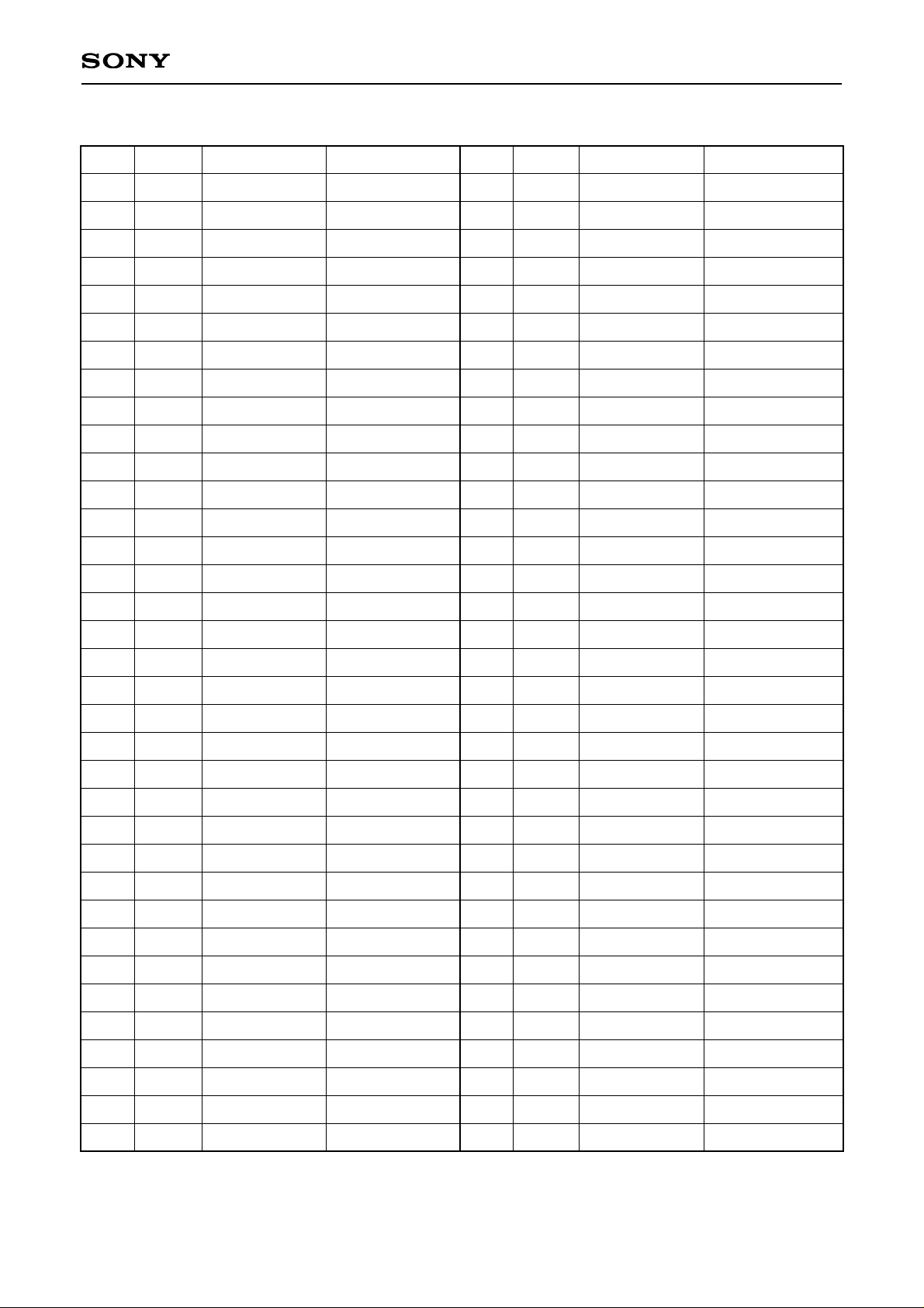
Pin Description of Panel Block
Pin No. Symbol Description Comment Pin No. Symbol Description Comment
1
2
3
4
5
6
7
8
9
10
11
12
13
14
15
16
17
18
19
20
21
22
23
24
25
26
27
28
29
30
31
32
33
34
35
36
37
38
39
40
41
42
43
44
45
46
47
48
49
50
51
52
53
54
55
56
57
58
59
60
61
62
63
64
65
66
67
68
69
70
TEST4
TEST5
TEST3
R31
R21
R11
R01
G31
G21
G11
G01
B31
B21
B11
B01
XR31
XR21
XR11
XR01
XG31
XG21
XG11
XG01
XB31
XB21
XB11
XB01
VCOM
VV
DD
VVSS1
VVSS2
VST
XVST
ENB
XENB
VCK
XVCK
TEST1
TEST2
RESET
HV
DD
HVSS1
HVSS2
HCK1
XHCK1
HCK2
XHCK2
HST1
XHST1
HST2
XHST2
OE1
XOE1
OE2
XOE2
V0
V1
V2
V3
V4
V5
V6
V7
V8
XB02
XB12
XB22
XB32
XG02
XG12
Test input
Test input
Test output
Data input
Data input
Data input
Data input
Data input
Data input
Data input
Data input
Data input
Data input
Data input
Data input
Data input
Data input
Data input
Data input
Data input
Data input
Data input
Data input
Data input
Data input
Data input
Data input
Common voltage
Power supply
GND
Power supply
Pulse input
Pulse input
Pulse input
Pulse input
No connection
No connection
Connected to R/C
Connected to 0V
Connected to 3.3V
No connection
Pulse input
Pulse input
Test output
Test output
Power-on reset
Power supply
GND
Power supply
Pulse input
Pulse input
Pulse input
Pulse input
Pulse input
Pulse input
Pulse input
Pulse input
Pulse input
Pulse input
Pulse input
Pulse input
Reference voltage
Reference voltage
Reference voltage
Reference Voltage
Reference voltage
Reference voltage
Reference voltage
Reference voltage
Reference voltage
Data input
Data input
Data input
Data input
Data input
Data input
– 5 –
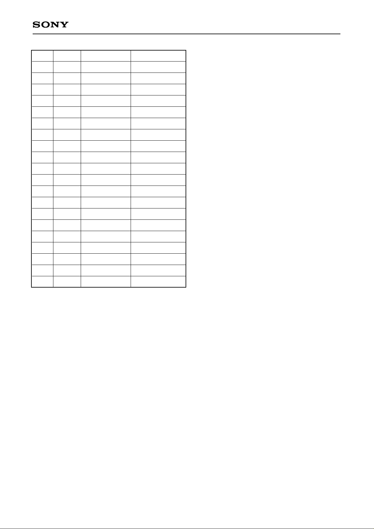
ACX704AKM
Pin No. Symbol Description Comment
71
72
73
74
75
76
77
78
79
80
81
82
83
84
85
86
87
88
89
90
XG22
XG32
XR02
XR12
XR22
XR32
B02
B12
B22
B32
G02
G12
G22
G32
R02
R12
R22
R32
TEST6
TEST7
Data input
Data input
Data input
Data input
Data input
Data input
Data input
Data input
Data input
Data input
Data input
Data input
Data input
Data input
Data input
Data input
Data input
Data input
Test input
Test input
Connected to 0V
Connected to 3.3V
– 6 –
ACX704AKM
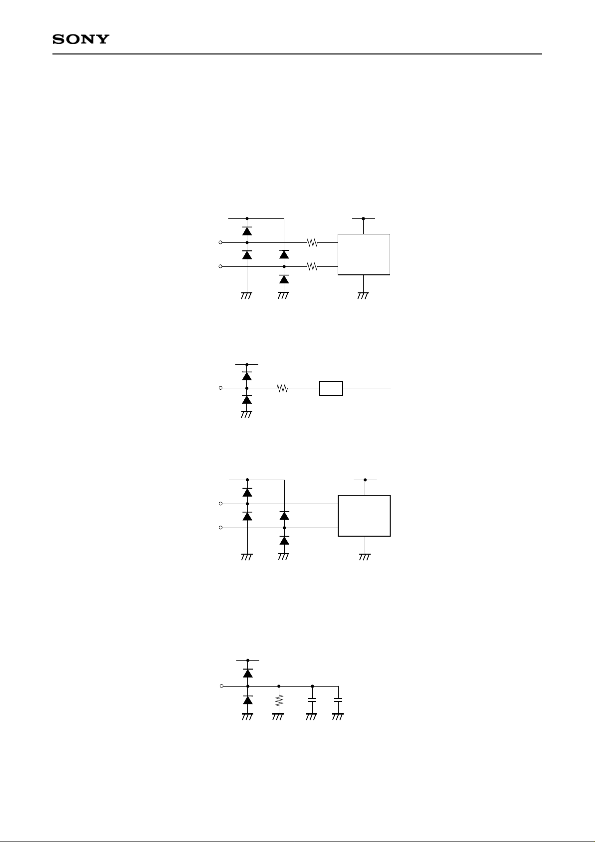
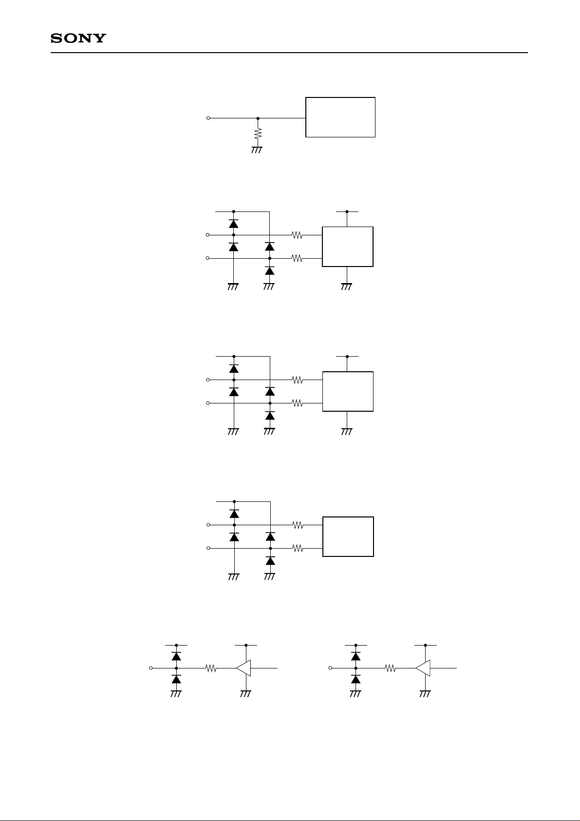
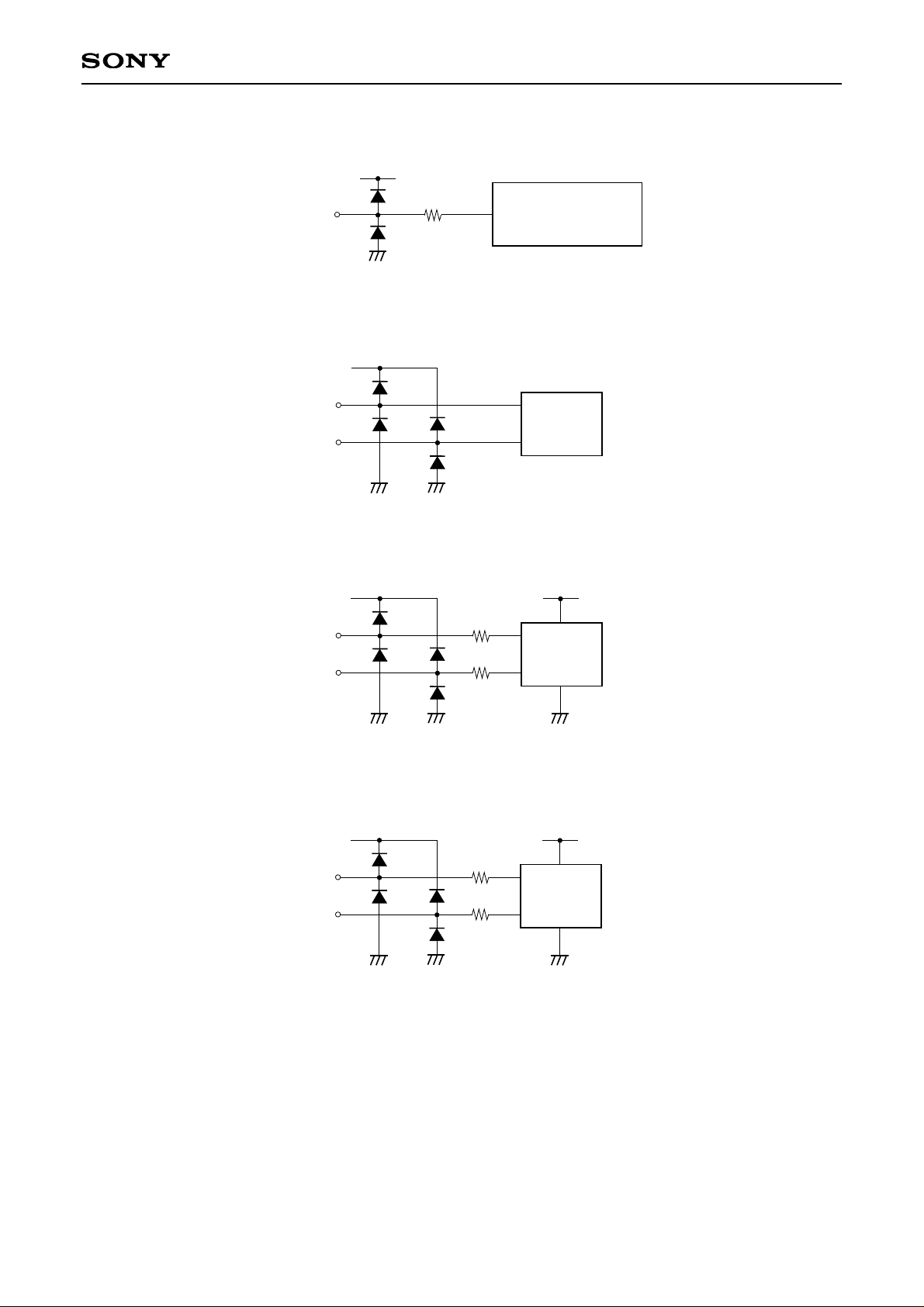
Input Equivalent Circuits of Panel Block
To prevent static charges, protective diodes are provided for each pin except the power supplies. In addition,
protective resistors are added to all pins except the reference input pins, data input pins, HCK1, XHCK1, HCK2
and XHCK2. Reference input pins and VCOM are connected to HVSS1 with a high resistance of 2MΩ (typ.).
The equivalent circuit of each pin is shown below.
(Resistor value: typ.)
(1) TEST4, TEST5
180Ω
180Ω
HVDD
HVSS1
TEST4
TEST5
HVDD
HVSS1
Level
conversion
circuit × 2
(2) TEST3
HVDD
HVSS1
TEST3
40Ω
Signal line
SW
(3) Data, XData
HVDD
HVDD
HVSS1HVSS1
Data
XData
Sampling
latch circuits
(4) VCOM
HVDD
HVSS1HVSS1
VCOM
2MΩ Cs LC
∗
Data means Rmn, Gmn, Bmn. (n = 0, 1, 2, 3, m = 1, 2)
XData means XRmn, XGmn, XBmn. (n = 0, 1, 2, 3, m = 1, 2)
– 7 –
ACX704AKM
(5) VVSS2
HVSS1
VVSS2
2MΩ
V driver and
level conversion
circuits
(6) VST, XVST
850Ω
850Ω
VVDD
VVSS1
VST
XVST
VVDD
VVSS1
Level
conversion
circuit × 2
(7) ENB, XENB
850Ω
850Ω
VVDD
VVSS1
EBN
XEBN
VVDD
VVSS1
Level
conversion
circuit × 1
(8) VCK, XVCK
40Ω
40Ω
VVDD
VVSS1
VCK
XVCK
V driver
(9) TEST1, TEST2
VVDD
VVSS1
VVDD
VVSS1
TEST1
40Ω
HVDD
HVSS1
HVDD
HVSS1
TEST2
40Ω
– 8 –
ACX704AKM
(10) RESET
HVDD
HVSS1
RESET
40Ω
H driver, V driver and
level conversion circuits
(11) HCKn, XHCKn (n = 1, 2)
HVDD
HVSS1
HCKn
XHCKn
H driver
(12) HSTn, XHSTn (n = 1, 2)
180Ω
180Ω
HVDD
HVSS1
HSTn
XHSTn
HVDD
HVSS1
Level
conversion
circuit × 4
(13) OEn, XOEn (n = 1, 2)
850Ω
850Ω
HVDD
HVSS1
OEn
XOEn
HVDD
HVSS1
Level
conversion
circuit × 2
– 9 –
ACX704AKM
(15) TEST6, TEST7
850Ω
850Ω
VVDD
VVSS1
TEST6
TEST7
VVDD
VVSS1
Level
conversion
circuit × 1
(14) Reference voltage input V0-V8
V0
V1
V2
V3
V4
V5
V6
V7
V8
HVDD
HVSS1HVSS1
Decoder
450Ω
450Ω
450Ω
450Ω
450Ω
450Ω
450Ω
450Ω
450Ω
450Ω
450Ω
450Ω
450Ω
450Ω
2MΩ
2MΩ
2MΩ
2MΩ
2MΩ
2MΩ
2MΩ
2MΩ
2MΩ
– 10 –
ACX704AKM
Operating Condition
Item Symbol Min. Typ. Max. Unit Pin/Remark
Supply voltage 1
Supply voltage 2
Supply voltage 3
Supply voltage 4
Reset voltage
Data/pulse input (Low)
Data/pulse input (High)
Common voltage center
Common voltage swing
Reference voltage 1
Reference voltage 2
Vertical frequency
Horizontal frequency
Data frequency
VCOM rise time
VCOM fall time
V0-V8 rise time
V0-V8 fall time
Data rise time
Data fall time
HST rise time
HST fall time
HCK rise time
HCK fall time
OE1 pulse rise time
OE1 pulse fall time
OE2 pulse rise time
OE2 pulse fall time
VST pulse rise time
VST pulse fall time
VCK pulse rise time
VCK pulse fall time
ENB pulse rise time
ENB pulse fall time
HCK duty
Cross point time lag
Data setup time 1
Data setup time 2
HVDD
VVDD
HVSS2
VVSS2
Vreset
VIL
VIH
VcomC
VcomA
Vref1
Vref2
fv
fh
fdot
trvcom
tfvcom
trvn
tfvn
trdata
tfdata
trhst
tfhst
trhck
tfhck
troe1
tfoe1
troe2
tfoe2
trvst
tfvst
trvck
tfvck
trenb
tfenb
Dhck
tdcross
tstp1
tstp2
8.5
8.5
–7.0
–7.0
HVDD – 0.1
–0.3
3.0
0.0
0.5
48
–15
35
35
9.0
9.0
–6.5
–6.5
HVDD
0.0
3.3
5.0
60
15.84
2.79
50
0
50
50
9.5
9.5
–6.0
–6.0
HVDD + 0.1
0.3
3.6
5.0
4.5
65
17.16
3.02
12.5
12.5
12.5
12.5
40
40
30
30
30
30
60
60
60
60
60
60
60
60
80
80
52
15
120
120
V
V
V
V
V
V
V
V
V
V
V
Hz
kHz
MHz
µs
µs
µs
µs
ns
ns
ns
ns
ns
ns
ns
ns
ns
ns
ns
ns
ns
ns
ns
ns
%
ns
ns
ns
HVDD
VVDD
HVSS2
VVSS2
RESET,
∗1
∗2
∗2
VCOM,
∗3
VCOM
V0, V1, V8
V2, V3, V4, V5, V6, V7
VCOM
VCOM
∗4
∗4
∗5
∗5
HST1, XHST1, HST2, XHST2
HST1, XHST1, HST2, XHST2
HCK1, XHCK1, HCK2, XHCK2
HCK1, XHCK1, HCK2, XHCK2
OE1, XOE1
OE1, XOE1
OE2, XOE2
OE2, XOE2
VST, XVST
VST, XVST
VCK, XVCK
VCK, XVCK
ENB, XENB
ENB, XENB
∗6
∗7
∗8
∗8
 Loading...