


GM 47/GM 48
Design Guidelines

CE
The product described in this manual conforms to the TTE directive 91/263/EEC and EMC directive
89/336/EEC. The product fulfils the requirements according to ETS 300 342-1.
The information contained in this document is the proprietary information of Sony Ericsson Mobile
Communications. The contents are confidential and any disclosure to persons other than the officers,
employees, agents or subcontractors of the owner or licensee of this document, without the prior written
consent of Sony Ericsson Mobile Communications , is strictly prohibited.
Further, no portion of this publication may be reproduced, stored in a retrieval system, or transmitted in
any form or by any means, electronic or mechanical, including photocopying and recording, without the
prior written consent of Sony Ericsson Mobile Communications , the copyright holder.
First edition (January 2002)
Sony Ericsson Mobile Communications . publishes this manual without making any warranty as to the
content contained herein. Further Sony Ericsson Mobile Communications . reserves the right to make
modifications, additions and deletions to this manual due to typographical errors, inaccurate information,
or improvements to programs and/or equipment at any time and without notice. Such changes will,
nevertheless be incorporated into new editions of this manual.
All rights reserved.
© Sony Ericsson Mobile Communications ., 2002
Publication number:
Printed in UK
Trademarks
AIX is a trademark owned by International Business Machines Corporation

GM47/48 Design Guidelines
Contents
1 INTRODUCTION ...........................................................................................................5
1.1 OVERVIEW ...............................................................................................................5
1.2 PRECAUTIONS...........................................................................................................5
1.3 ABBREVIATIONS ........................................................................................................5
2 MECHANICAL INTEGRATION.......................................................................................7
2.1 PHYSICAL DIMENSIONS...............................................................................................7
3 ELECTRICAL INTEGRATION........................................................................................8
3.1 GENERAL.................................................................................................................8
3.2 GROUNDING .............................................................................................................9
3.2.1 The Analogue Ground .......................................................................................9
3.2.2 The Digital Ground (DGND)...............................................................................9
3.3 EXTERNAL SUPPLY TO MODULE................................................................................. 10
3.3.1 Power Supply (VCC) .......................................................................................10
3.4 GENERAL RECOMMENDATIONS .................................................................................. 11
3.5 SIM CONNECTIONS.................................................................................................. 13
3.6 AUDIO CONNECTIONS............................................................................................... 14
3.6.1 Analogue Audio.............................................................................................. 14
3.6.2 Advanced Portable Hands Free Functionality ...................................................15
3.7 RF AND ANTENNA INTEGRATION .................................................................................16
3.8 INTERFACING TO A 3.3V µPROCESSOR....................................................................... 17
3.9 SOFTWARE DOWNLOAD AND LOGGING CIRCUITRY ......................................................... 17
4 DEVELOPERS BOARD............................................................................................... 18
4.1 POWER CIRCUIT...................................................................................................... 18
4.2 SIM CIRCUIT.......................................................................................................... 18
5 PART NUMBERS ........................................................................................................20
5.1 SYSTEM CONNECTOR............................................................................................... 20
5.2 RF CONNECTOR...................................................................................................... 20
5.3 SIM CARD HOLDER.................................................................................................. 20
5.4 SUPPLIERS............................................................................................................. 20
5.4.1 Imperial connectors ........................................................................................ 20
5.4.2 IMS connectors .............................................................................................. 21
6 TYPE APPROVAL....................................................................................................... 22
6.1 DOCUMENTATION REQUIRED...................................................................................... 22
6.2 POWER SUPPLY ...................................................................................................... 22
6.3 SIM TESTING.......................................................................................................... 23
6.4 EMC/ESD & SAFETY .............................................................................................. 23
6.5 RF TESTING........................................................................................................... 23
6.5.1 GM47............................................................................................................. 23
6.5.2 GM48............................................................................................................. 23
6.6 SAR WARNING ........................................................................................................24
6.7 OTHER TA ISSUES ...................................................................................................24
6.7.1 External Application software........................................................................... 24
6.7.2 GM47 software updates .................................................................................. 24
APPENDIX I - TECHNICAL DATA ...................................................................................... 25
APPENDIX II – GM47/48 PIN OUT ......................................................................................27
BA/SEM/MSC 02:0006 Rev PA1 3

GM47/48 Design Guidelines
APPENDIX III GSM TRANSMIT WAVEFORM CHARACTERISTICS .....................................30
BA/SEM/MSC 02:0006 Rev PA1 4

1 Introduction
1.1 Overview
1.2 Precautions
GM47/48 Design Guidelines
The GM47/48 belong to a new generation of Sony Ericsson Mobile
Communications GSM modules. This document describes the main
characteristics and functionality of the GM 47/48, two dual band
products for 900/ 1800 MHz and 850/1900 MHz GSM bands
respectively.
This document should be used in conjunction with either the GM 47/48
Integrators Manual or GM47/48 Technical Description and is intended
to aid the system integrator both designing the module into their
application and gaining the correct approvals.
The GM47/48 should be handled like any mobile station. In the
Integrators’ Manual you will find more information about safety and
product care. Never exceed these limits to ensure the module is not
damaged.
1.3 Abbreviations
Abbreviation Explanation
BT Bluetooth
CBS Cell Broadcast Service
CBM Cell Broadcast Messaging
CSD Circuit Switch Data
DCE Data Circuit Terminating Equipment
DTE Data Terminal Equipment
DTMF Dual Tone Multi Frequency
EFR Enhanced Full Rate codec
EMC Electro-Magnetic Compatibility
ETSI European Telecommunications Standards Institute
FR Full Rate codec
GPRS General Packet Radio Service
GPS Global Positioning System
GSM Global System for Mobile Comunication
HR Half Rate codec
HSCSD High Speed Circuit Switched Data
ITU-T International Telecommunication Union – Telecommunications
Standardisation Sector
ME Mobile Equipment
BA/SEM/MSC 02:0006 Rev PA1 5

GM47/48 Design Guidelines
MO Mobile Originated
MS Mobile Station
MT Mobile Terminated
PCM Pulse Code Modulation
PDU Protocol Data Unit
RLP Radio Link Protocol
RF Radio Frequency
RTC Real Time Clock
SDP Service Discovery Protocol
SMS Short Message Service
SIM Subscriber Identity Module
TBD To Be Defined
BA/SEM/MSC 02:0006 Rev PA1 6
GM47/48 Design Guidelines
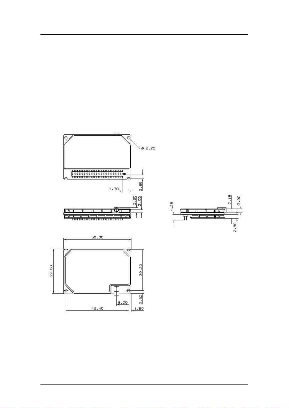
2 Mechanical Integration
The GM 47/48 are protected with AISI 304 Stainless Steel covers
suitable to fulfil the environmental and EMC requirements.
Dimensions, the position of the different connectors and mounting
holes are shown in figure 2.1.
2.1 Physical Dimensions
Figure 2.1 Physical dimensions of GM 47/48
BA/SEM/MSC 02:0006 Rev PA1 7
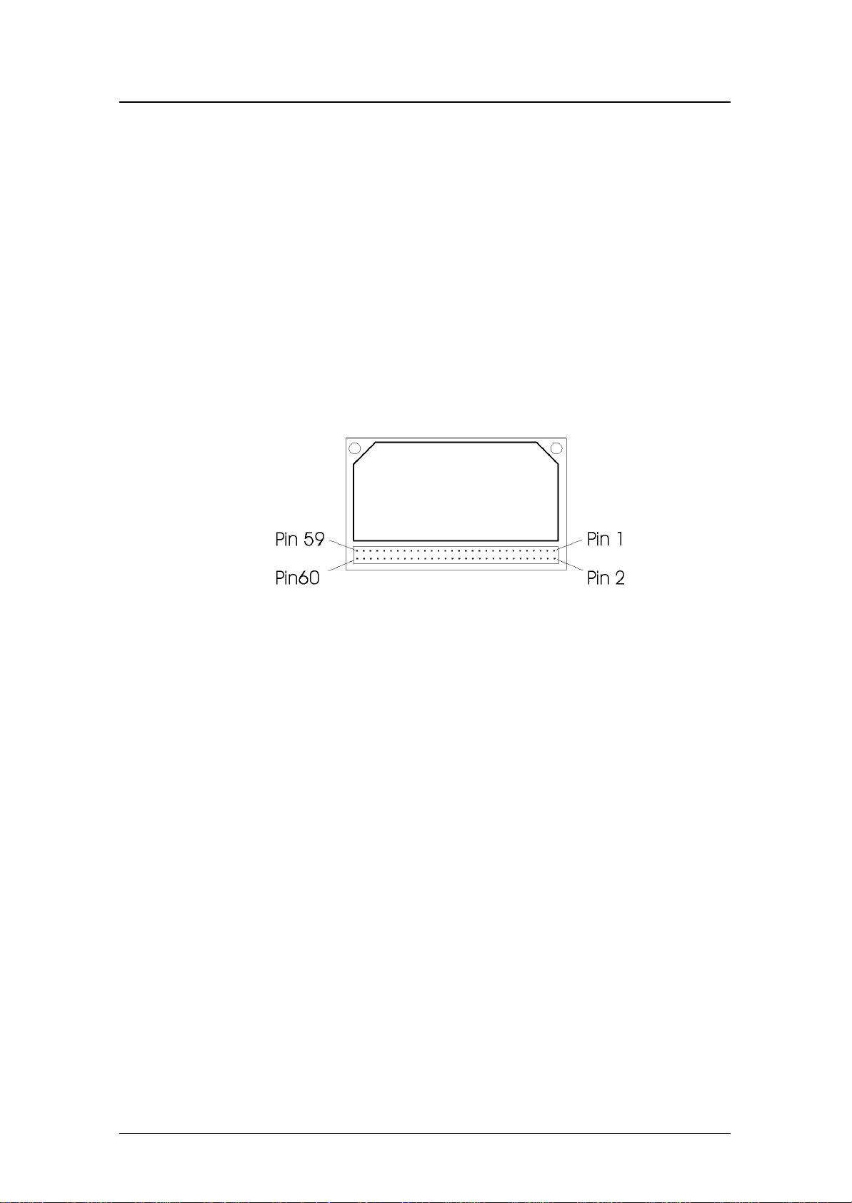
3 Electrical Integration
3.1 General
The electrical connections to the module (except the antenna ), are set
through the System Connector Interface.
The connector shall allow the following connections: board to board
and board to cable.
See section 5 for suppliers and part numbers.
The figure 3.1 below indicates the pin numbering scheme.
GM47/48 Design Guidelines
Figure 3.1 GM 47/48. View from the underside
BA/SEM/MSC 02:0006 Rev PA1 8

GM47/48 Design Guidelines
3.2 Grounding
Pins Name Description
2, 4, 6, 8, 10, 12 DGND Digital Ground
60 AGND Analogue Ground
There are two ground signals in GM 47/48, Analogue Ground (AGND)
and Digital Ground (DGND). The analogue Ground is connected to pin
number 60, and the Digital Ground is connected to the System
Connector Interface through pin numbers 2, 4, 6, 8, 10 and 12.
Note: All the Ground pins have to be connected to the application. The
AGND is connected to the DGND in the ME, and only there. It is
important that the AGND and the DGND are separated in the
application.
3.2.1 The Analogue Ground
The AGND lead is the analogue audio reference ground. It is the return
signal for Audio To Mobile Station (ATMS) and Audio From Mobile
Station (AFMS).
It is connected to the Digital Ground (DGND) inside the module and
only there. The application shall not connect DGND and AGND.
Parameter Limit
I
max ≅12.5mA
3.2.2 The Digital Ground (DGND)
DGND is the reference for all digital signals in the System Interface.
It shall also be the DC return for the power supply on VCC and
SERVICE. Each DGND pin is rated at 0.5 A. All DGND pins are
connected internally in the module.
Parameter Limit
I
average
I
max
BA/SEM/MSC 02:0006 Rev PA1 9
< 0.5 A No DGND pin can withstand over 0.5 A
< 600 mA (100 mA each)
GM47/48 Design Guidelines
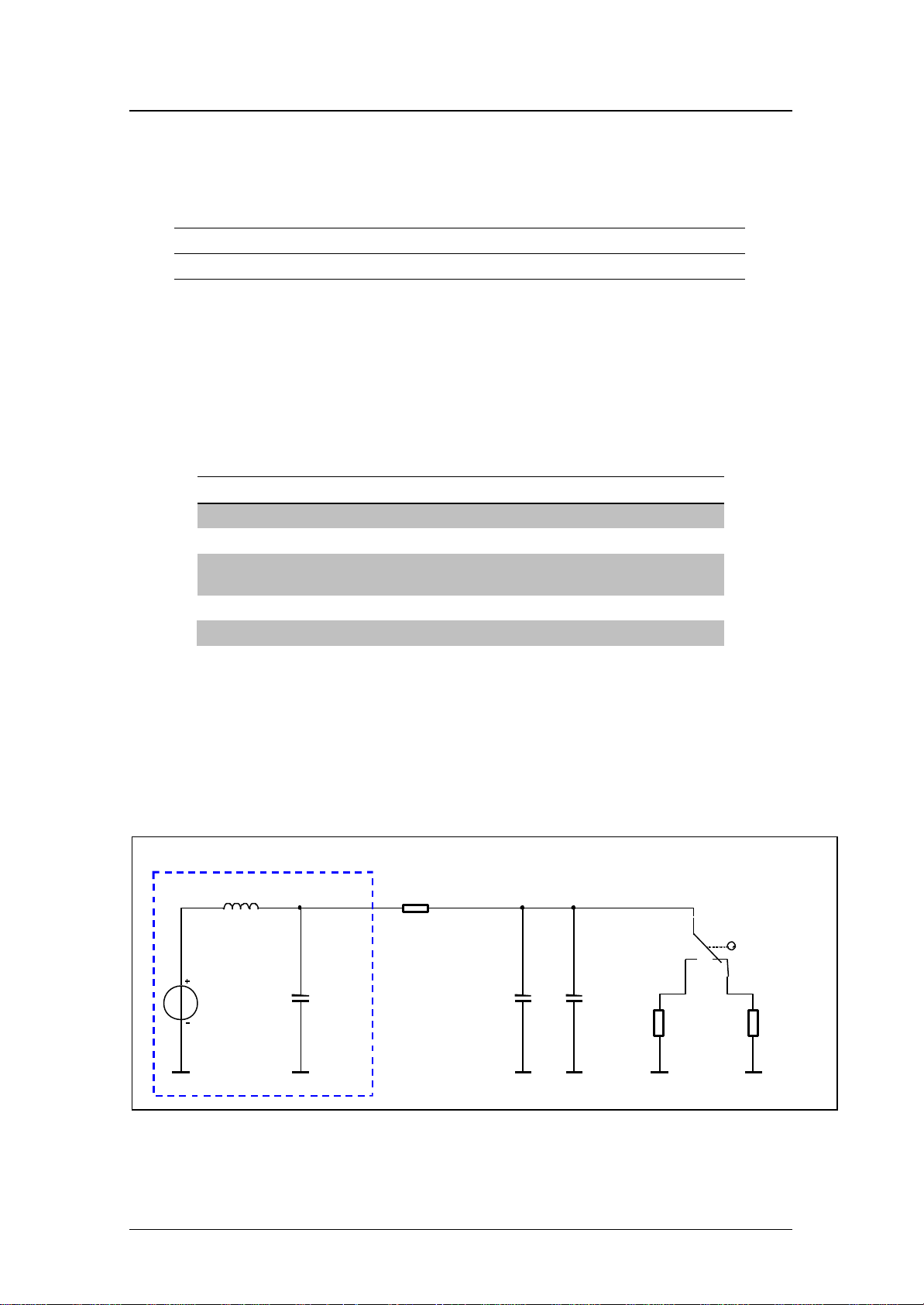
+++
Vcc
3.3 External Supply to Module
Pins Name Description
1, 3, 5, 7, 9, 11 VCC Regulated Power Supply
Connect all of the pins together in the application in order to carry the
current drawn by the module.
3.3.1 Power Supply (VCC)
The VCC supplies the module with external power. Any other voltage
needed is generated internally.
Parameter Mode Limit
Voltage to be applied Nominal 3.6 Volts
Tolerance 3.4 Volts - 4.0 Volts
Maximum voltage drop during
transmit burst
Over voltages 5.5 Volts
Current Drive capability at TX Full Power < 600 mA (average))
200mV
< 2 A (Peak)
33uH
V1
2 Amp
L1
GM 47/48 does not have internal capacitance to supply the large
current peaks during GSM transmission. Therefore on burst
transmission the application DC source is responsible for providing the
appropriate current.
Recommendations to the design of power supplies are given in the
following sections.
'R
' represents resistance
LINE
of circuit between PSU and
GM47/GM48.
3.6V
C1
220uF
RLINE
100mohm
CF
100uF
Low ESR
CBULK
1000uF
Low ESR
RRX
120ohm
30mA Load
J1
577usec
1:8 Duty Cycle
RTX
1.8ohm
2A Load
Figure 3.2 - Simplified Power Supply Reference Model
BA/SEM/MSC 02:0006 Rev PA1 10
 Loading...