

Sony 1000RF - CDX CD Player Service Manual
1
Model Name Using Similar Mechanism CDX-2500R
CD Drive Mechanism Type MG-363X-121
Optical Pick-up Name KSS-521A
SERVICE MANUAL
US Model
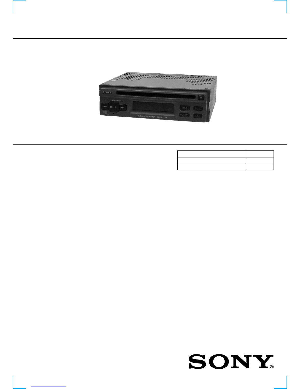
CDX-1000RF
COMPACT DISC PLAYER
AUDIO POWER SPECIFICATIONS
POWER OUTPUT AND TOTAL HARMONIC DISTORTION
13 watts per channel minimum continuous average power into
4 ohms, 4 channels driven from 20 Hz to 20 kHz with no more
than 1% total harmonic distortion.
Other Specifications
CD player section
System Compact disc digital audio
system
Signal-to-noise ratio 90 dB
Frequency response 10 – 20,000 Hz
Wow and flutter Below measurable limit
Laser Diode Properties
Material GaAs+GaAlAs
Wavelength 785 – 815 nm (Typ. 800 nm)
Emission Duration Continuous
Laser output power Less than 0.5 mW*
* This output is the value measured at a distance
of 0.7 mm from the objective lens surface on the
Optical Pick-up Block.
SPECIFICATIONS
General
Outputs Line outputs
Power requirements 12 V DC car battery
(negative ground)
Current drain 2A (at disc loading)
Dimensions Approx. 178 × 50 × 173 mm
(7 1/8 × 2 × 6 7/8 in.)
(w/h/d)
Mounting dimensions Approx. 182 × 53 × 159 mm
(7 1/4 × 2 1/8 × 6 3/8 in.)
(w/h/d)
Mass Approx. 1.1 kg (2 lb. 7 oz.)
Supplied accessories Parts for installation and
connections (1 set)
Design and specifications are subject to change without
notice.

2
TABLE OF CONTENTS
1. GENERAL
Location of controls................................................................. 3
Getting Started......................................................................... 3
Operation ................................................................................. 3
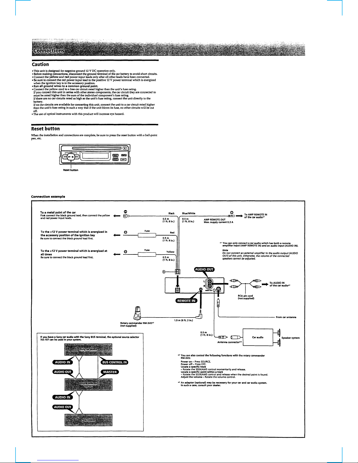
Connections ............................................................................. 4
2. DISASSEMBLY
2-1. Panel Assy, Front ................................................................. 5
2-2. CD Mechanism Block ......................................................... 5
2-3. Main Board ......................................................................... 6
2-4. Chassis (Rear) ..................................................................... 6
2-5. Chassis (T) Sub Assy .......................................................... 7
2-6. Lever Assy ........................................................................... 7
2-7. Servo Board......................................................................... 8
2-8. Roller Assy.......................................................................... 8
2-9. Chassis (OP) (O/S) Assy ..................................................... 9
2-10. Optical Pick-up Block ......................................................... 9
3. ELECTRICAL ADJUSTMENTS
CD Section ............................................................................10
4. DIAGRAMS
4-1. IC Pin Description............................................................. 11
4-2. Block Diagram –CD Section (1/2)– .................................. 12
4-3. Block Diagram –CD Section (2/2)– .................................. 13
4-4. Block Diagram –Display, Power Supply Section– ............ 14
4-5. Circuit Boards Location .................................................... 15
4-6. Printed Wiring Boards –CD Mechanism Section–............ 16
4-7. Schematic Diagram –CD Mechanism Section– ................ 17
4-8. Printed Wiring Board –Main Section– .............................. 18
4-9. Schematic Diagram –Main Section (1/2)– ........................ 19
4-10. Schematic Diagram –Main Section (2/2)– ........................ 20
4-11. Schematic Diagram –Display Section–............................. 21
4-12. Printed Wiring Board –Display Section– .......................... 22
5. EXPLODED VIEWS
5-1. Chassis Section ................................................................. 26
5-2. Front Panel Section ........................................................... 27
5-3. CD Mechanism Section (1) ............................................... 28
5-4. CD Mechanism Section (2) ............................................... 29
5-5. CD Mechanism Section (3) ............................................... 30
6. ELECTRICAL PARTS LIST ........................................ 31
SAFETY-RELATED COMPONENT WARNING!!
COMPONENTS IDENTIFIED BY MARK 0 OR DOTTED LINE
WITH MARK 0 ON THE SCHEMATIC DIAGRAMS AND IN
THE PARTS LIST ARE CRITICAL TO SAFE OPERATION.
REPLACE THESE COMPONENTS WITH SONY PARTS WHOSE
P ART NUMBERS APPEAR AS SHOWN IN THIS MANU AL OR
IN SUPPLEMENTS PUBLISHED BY SONY.
SERVICE NOTE
CAUTION
Use of controls or adjustments or performance of procedures other than those specified herein may result in hazardous radiation exposure.
Notes on Chip Component Replacement
• Never reuse a disconnected chip component.
• Notice that the minus side of a tantalum capacitor may be dam-
aged by heat.
NOTES ON HANDLING THE OPTICAL PICK-UP BLOCK
OR BASE UNIT
The laser diode in the optical pick-up block may suffer electrostatic
breakdown because of the potential difference generated by the
charged electrostatic load, etc. on clothing and the human body.
During repair, pay attention to electrostatic breakdown and also use
the procedure in the printed matter which is included in the repair
parts.
The flexible board is easily damaged and should be handled with
care.
NOTES ON LASER DIODE EMISSION CHECK
The laser beam on this model is concentrated so as to be focused on
the disc reflective surface by the objective lens in the optical pickup block. Therefore, when checking the laser diode emission, observe from more than 30 cm away from the objective lens.
NOTES ON PICK-UP FLEXIBLE BOARD
The pick-up flexible board in this set is secured to the optical pickup with an adhesive tape. Once the tape is removed, an adhering
force becomes weak, and it cannot be reused.
Therefore, if the optical pick-up is replaced, replace also the pickup flexible board with a new one.
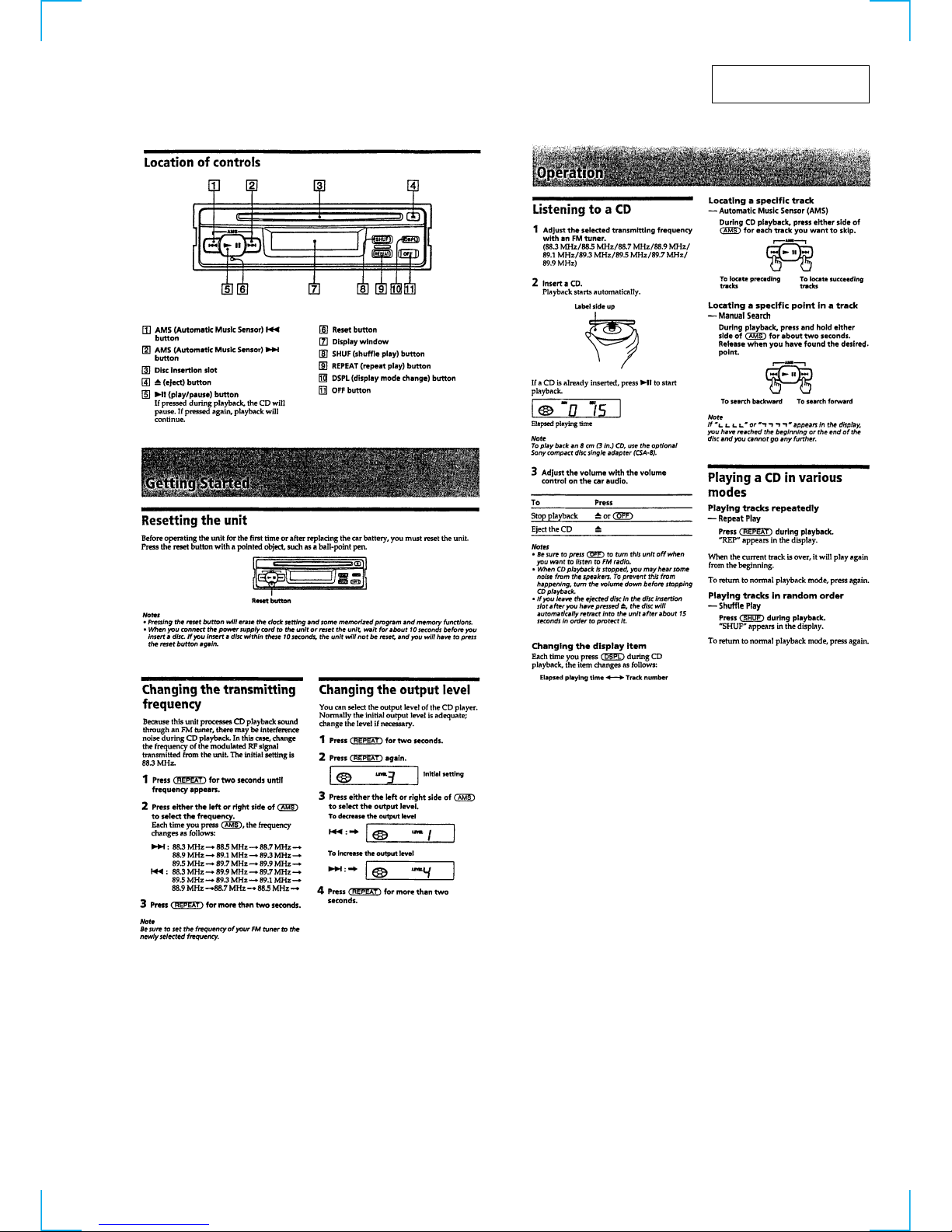
3
SECTION 1
GENERAL
This section is extracted
from instruction manual.
4
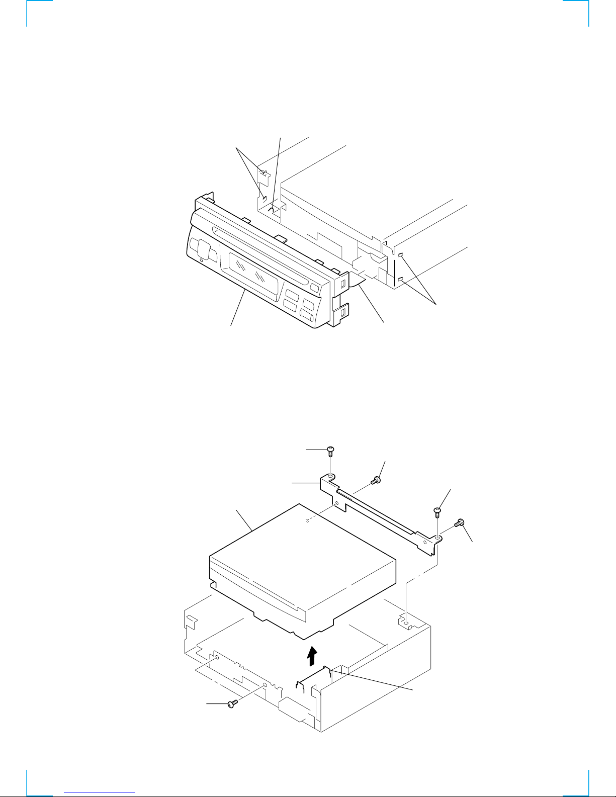
5
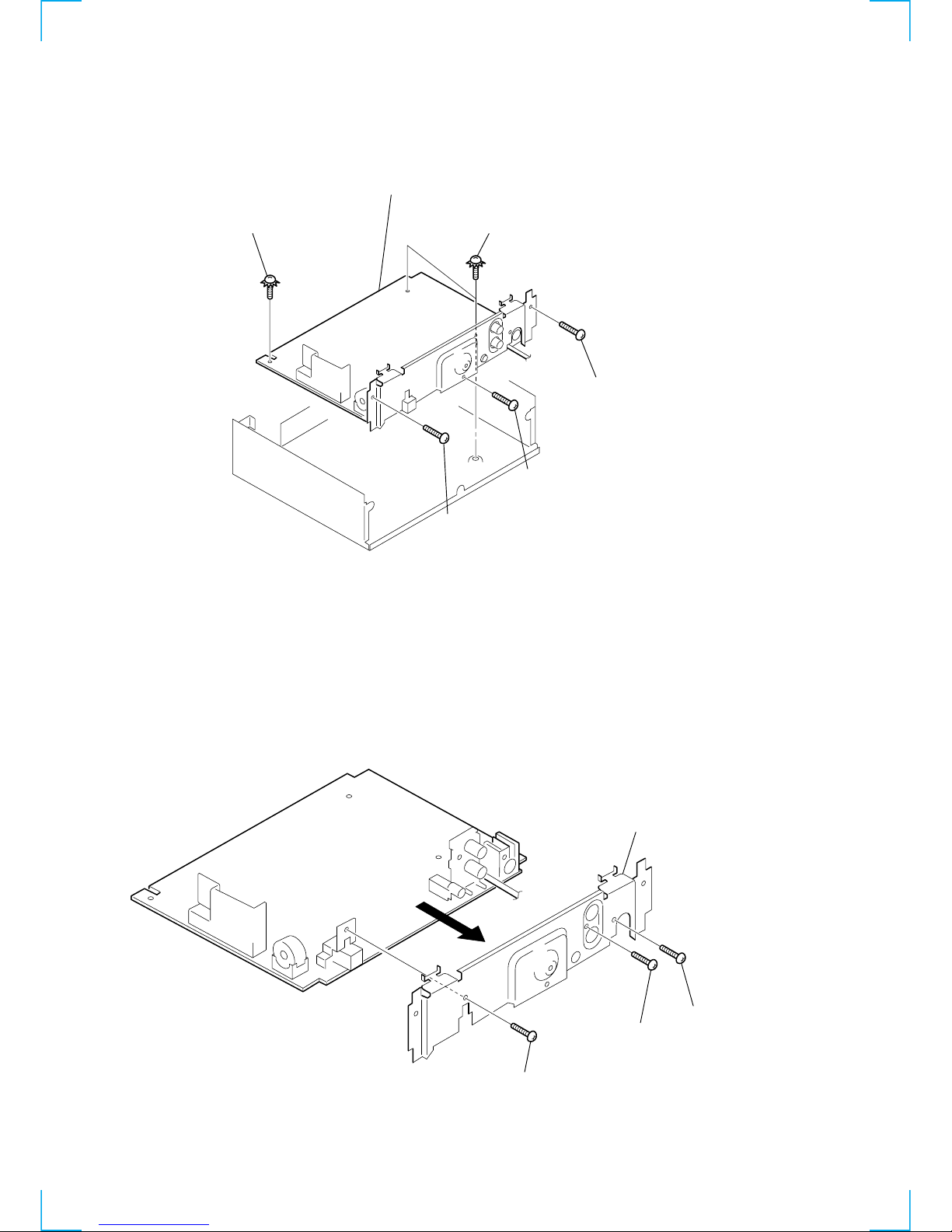
3 claw
1 claws
4 CNP801
5 panel assy, front
2 claws
7 PTT 2.6x6
3 PTT 2.6x6
6 PTT 2.6x
6
2 PTT 2.6x6
4 CNP701
8 bracket (M/D)
5 CD mechanism block
1 PTT 2.6x6
SECTION 2
DISASSEMBLY
Note : Follow the disassembly procedure in the numerical order given.
2-1. PANEL ASSY, FRONT
2-2. CD MECHANISM BLOCK
6
2 PTT 2.6x6
4 chassis (rear)
1 PTT 2.6x6
3 PTT 2.6x
6
4 ground point screws
(PTT 2.6x6)
5 ground point screw
(PTT 2.6x6)
1 PTT 2.6x6
6 MAIN board
3 PTT 2.6x
6
2 PTT 2.6x6
2-3. MAIN BOARD
2-4. CHASSIS (REAR)
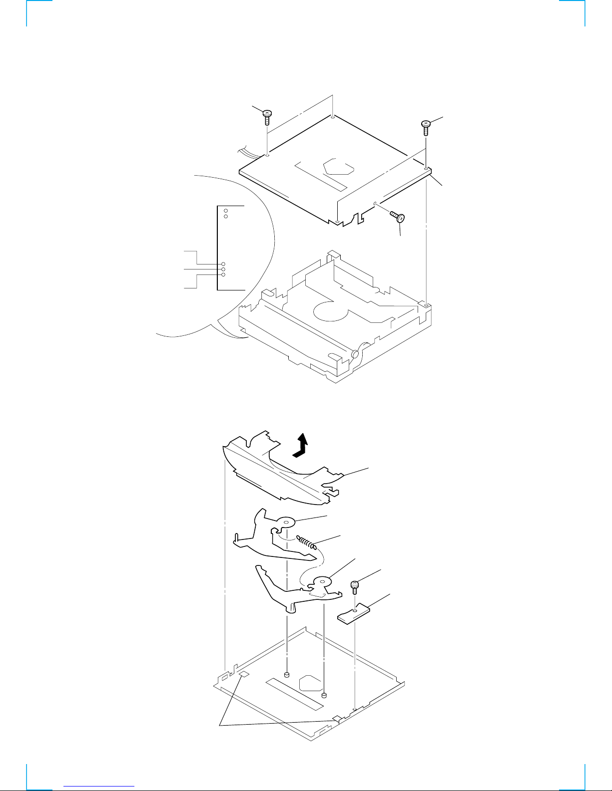
7
4 claws
2 DISC IN SW board
7 lever (L) assy
3 tension spring (LR)
6 lever (R) assy
5 guide (disc)
1 PS 2x4
5 chassis (T) sub assy
3 P 2x3
4 P 2x3
1 Unsolder the
lead wires.
red
white
black
2 P 2x3
2-5. CHASSIS (T) SUB ASSY
2-6. LEVER ASSY
8
Fig. 1
4 PS 2x3
5 LOAD SW board
1 tension spring (RA)
2 arm (roller)
3 roller assy
washer
arm
arm
ring (roller), retaining
spacer, insulating
7 PS 2x4
1 CN3
3 Removal the solders.
4 Removal the solders.
5 P 2x3
6 loading motor assy
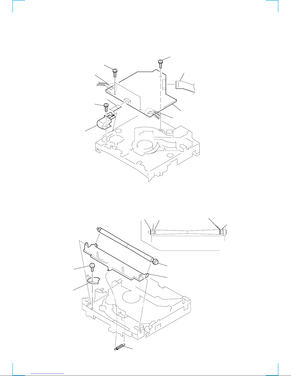
9 SERVO board
2 CN2
8 PS 2x4
2-7. SERVO BOARD
2-8. ROLLER ASSY
• When installing, take note of the positions
arm (roller) and washers. (Fig. 1)
9
1 tension spring (KF1)
8 compression spring (FL)
7 chassis (OP) (O/S) assy
9 compression spring (FL)
2 tension spring (KR1)
5 Fit lever (D) in the
direction of the arrow.
3 damper (T)
4 damper (T)
6 Turn loading ring in the
direction of the arrow.
1 P 2x3
2 sled motor assy
3 optical pick-up block
2-9. CHASSIS (OP) (O/S) ASSY
2-10. OPTICAL PICK-UP BLOCK
10
IC3
CN1
IC1
CN2
FOCUS GAIN ADJ
RV4
TP
(RF. GND)
IC2
TP
(RF)
CN3
RV1
FOCUS BIAS ADJ
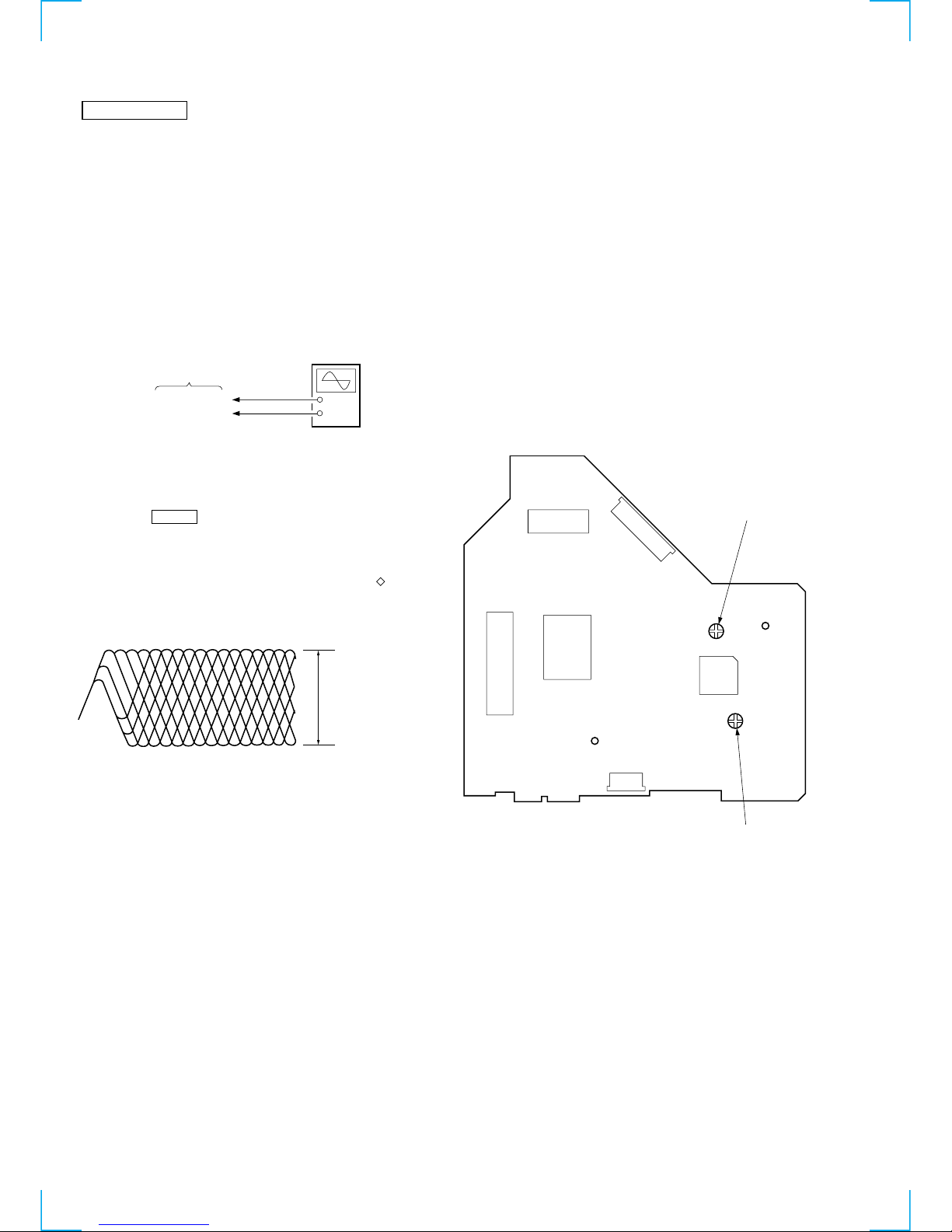
RF signal waveform
VOLT/DIV: 200 mV
TIME/DIV: 500 nS
level: 1.0 – 1.5 Vp-p
SERVO board
TP (RF)
TP (RF. GND)
oscilloscope
+
–
CD SECTION
Note:
1. CD Block basically constructed to operate without adjustment.
Therefore, check each item in order given.
2. Use YEDS-18 disc (3-702-101-01) unless otherwise indicated.
3. Use the oscilloscope with more than 10 MΩ impedance.
4. Clean an objective lens by an applicator with neutral detergent
when the signal level is low than specif ied value with the f ollowing
checks.
Focus Bias Adjustment
Setting: This adjustment is performed with the set placed
horizontally.
Focus Gain Adjustment (Coarse adjustment)
This adjustment is not required unless the following parts are re placed:
• Optical pick-up
• RV4
Procedure:
1. Set RV4 to the standard position. (mechanical center)
2. Check whether operation noise (while noise type) caused by
the 2-axis device (lens section of the optical pick-up) is
abnormally loud.
If the operation noise is too loud, turn RV4 slightly counterclockwise.
• If the gain is too low:
Focus does not function and no music is selected.
• If the gain is too high:
Noise caused by scratches and dust is heard and the operation
becomes unstable.
Adjustment Location: servo board
Adjustment Location: servo board (component side)
Procedure:
1. Connect an oscilloscope between TP (RF) and TP (RF. GND)
on the SERVO board.
2. Connect the power supply.
3. Push the RESET button (S900) on the MAIN board.
4. Insert the disc (YEDS-18) and playback.
5. Adjust RV1 so that the oscilloscope w aveform is clear and check
RF signal level is correct or not.
Note: Clear RF signal waveform means that the sharp “ ” can be
clearly distinguished at the center of the waveform.
• When observing the ey e pattern, set the oscilloscope to A C range
and raise the vertical sensitivity so that it may be easily seen.
Adjustment Location: servo board
SECTION 3
ELECTRICAL ADJUSTMENTS
11 11
4-1. IC PIN DESCRIPTION
• IC801 µPD17705GC-547-3B9 (SYSTEM CONTROL)
Pin No. Pin Name I/O Pin Description
1 NC — Not used. (Connect to ground in this set.)
2 IN_SW I Disc insertion detection input L: IN_SW
3 D_SW I DOWN switch detection input L: D_SW
4 SELF_SW I Disc self store detection input L: SELF_SW
5 L_SW I Sled limit switch detection input L: L_SW
6 LM_EJ O Loading motor control output (Eject direction)
7 LM_LD O Loading motor control output (Loading direction)
8 RY_ON O Relay control output
9, 10 NC — Not used. (Open)
11 BAND_SW I BAND select input 0: US
12 – 20 NC — Not used. (Open)
21 GND3 — Ground
22 NC — Not used. (Open)
23 ADKI2 I A/D key input 2
24 ADKI1 I A/D key input 1
25 ROTCOM I Rotary commander shift key input
26 NC — Not used. (Open)
27 TEST_SW I Test mode initial setting detection input L: TEST_SW
28, 29 NC — Not used. (Open)
30 VDD2 — Power supply pin (+5 V)
31 FMIN I PLL local oscillator frequency input
32 NC — Not used. (Open)
33 GND2 — Ground
34 NC — Not used. (Open)
35 EO1 O PLL error 1 output
36 TEST0 — Connect to GND line.
37 – 40 NC — Not used. (Open)
41 ACC_IN I Accessory power detection input L: ACC_IN
42 SCOR I SCOR signal detection input
43 MUTE O Mute control output
44 LEVEL D O Level control output
45 NC — Not used. (Open)
46 PH2 I Connect to +5 V line.
47 LEVEL 1 O Volume control output
48, 49 NC O Not used. (Open)
50 EMPH_O O Emphasis control output
51 PW_ON O System power control output
52 LM_ON O Loading motor power control output
53 CD_ON O CD power control output
54 ILLON O Illumination power control output
55 – 57 NC — Not used. (Open)
58 LCD_CE O LCD chip enable output
59 EZ_SEL I Rotary commander shift key input L: EZ_SEL
60 SENS I CD SENS signal detection input
61 FOK I Focus OK signal detection input
62 LD_ON O Laser ON/OFF control output L: LD_ON
63, 64 NC — Not used. (Open)
65 LCD_CLK O LCD serial clock output
66 LCD_DAT O LCD serial data output
67 LCD_INH O LCD inhibition output L: LCD_INH
68 SQCK0 O Sub Q read clock output
SECTION 4
DIAGRAMS
Pin No. Pin Name I/O Pin Description
69 CD_RST O Reset output to CD signal processor IC.
70 SQ_SI I Sub Q data input
71 CD_SO0 O CD signal serial data output
72 CD_LAT O CD signal processing data latch output
73 CD_CK0 O CD signal processing serial clock output
74 NC — Not used. (Open)
75 GND1 — Ground
76 XOUT O ceramic oscillator output (4.5 MHz)
77 XIN I ceramic oscillator input (4.5 MHz)
78 BU_IN I Backup power detection input
79 VDD1 — Power supply pin (+5 V)
80 RESET I Reset input L: RESET
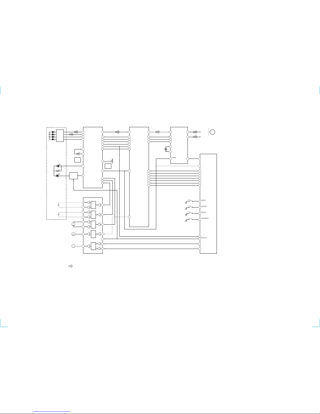
12 12
35 31
36
39
38
PD1 RF
CLKO
XLTO
DATO
SEIN
FOK
CNIN
RF 0
21
PCMD
22
BCK
20
LRCK
34
XTAI
19
CLK
20
XLT
21
DATA
24
SENS
25
FOK
23
14
DIN
59
57
56
54
1
55
C. OUT
37
FE BIAS
22 50
XRST
16
SL O
6
FE O
13
TA O
PD2
E
F
1
FEO
2
FEI
34
PD
33
LD
XRST
MDP
RF AMP, SERVO CONTROL
IC2
OPTICAL PICK-UP
KSS-521A
DIGITAL SIGNAL PROCESSOR
IC1
D/A CONVERTER
IC701
FOCUS
GAIN
RV4
FOCUS
BIAS
RV1
LD POWER
CONTROL
Q1, 2
PD
LD
FOCUS/TRACKING COIL DRIVE,
MOTOR DRIVE
IC3
CH2 IN
LEVEL
SHIFT
22
16
15
TRACKING
CH1 IN
LEVEL
SHIFT
19
18
17
FOCUS
M902
(SLED)
CH2+
CH2–
CH1+
CH1–
CH3 IN
LEVEL
SHIFT
24
13
14
CH3+
CH3–
M
M901
(SPINDLE)
CH4 IN
LEVEL
SHIFT
3
CTL2
5
12
CH4+
M
M903
(LOADING)
FWD
LEVEL
SHIFT
6
REV
7
10
CH5+
M
49
SENS
46
SQSO
47
SQCK
51
DATA
52
XLAT
53
CLOK
43
SCOR
5
BCKIN
6
LRCIN
4
CLKO
19
XTI
1
XTO
20
RSTB
15
12
VOUTL
9
VOUTR
17
MC/DM1
X701
16.9344MHz
3
SCOR
CD_CK0
CD_LAT
CD_SO0
SQCK0
SQ_SI
SENS
CD_RST
FOK
LD_ON
LM_EJ
LM_LD
L_SW
IN_SW
D_SW
SELF_SW
SW3
(LIMIT)
SW1
(DISC IN)
SW4
(DOWN)
SW2
(SELF)
61
62
42
5
2
3
4
73
72
71
68
70
60
69
EMPH_O
50
SYSTEM CONTROL
IC801 (1/3)
CD L-CH
CD R-CH
CD
SECTION
(2/2)
A
I-V
AMP
04
• Signal path
: CD
• R-ch : same as L-ch.
6
7
CDX-1000RF
4-2. BLOCK DIAGRAM — CD SECTION (1/2) —
(Page 13)
 Loading...