


USB3500
Hi-Speed USB Host,
Device or OTG PHY
With UTMI+ Interface
PRODUCT FEATURES
USB-IF “Hi -Speed” certified to the Universal Serial
Bus Specification Rev 2.0
Interface compl iant with the UTMI+ Specification,
Revision 1.0.
Inclu des full support for the optional On-The-Go
(OTG) protocol detailed in the On-The-Go
Supplement Revision 1.0a specification.
Function al as a host, device or OTG PHY.
Sup ports HS, FS, and LS data rates.
Sup ports FS pre-amble fo r FS hu bs with a LS device
attached (UTMI+ Level 3)
Sup ports HS SOF and LS keep alive pulse.
Supports Host Negotiation Protocol (HNP) and
Session Request protocol (SRP.)
Internal comparators support OTG monitoring of
VBUS levels.
Low Latency Hi-Speed Receiver (43 Hi-Speed clocks
Max)
Datasheet
Interna l 1.8 volt regulators allow operation from a
single 3.3 volt supply
Interna l short circuit protection of ID, DP and DM
lines to VBUS or ground.
Integrated 24MHz Crystal Oscillator supports either
crystal operation or 24MHz external clock input.
Interna l PLL for 480MHz Hi-Speed USB operation.
Su pports USB 2.0 and legacy USB 1.1 devices
55mA Unconfigured Current (typical) - ideal for bus
powered applications.
8 3uA suspend current (typical) - ideal for battery
powered applications.
Full Commercial operating temperature range from
0C to +70C
56 Pin, QFN lead-free RoHS compliant package
(8 x 8 x 0.90 mm height)
SMSC USB3500 DATASHEET Revision 1.0 (06-05-08)
Hi-Speed USB Host, Device or OTG PHY With UTMI+ Interface
ORDER NUMBER:
USB3500-ABZJ FOR 56 PIN, QFN LEAD-FREE ROHS COMPLIANT PACKAGE
Datasheet
80 ARKAY DRIVE, HAUPPAUGE, NY 11788 (631) 435-6000, FAX (631) 273-3123
Copyright © 2008 SMSC or its subsidiaries. All rights reserved.
Circuit diagrams and other information relating to SMSC products are included as a mean s of illustrating typical applications. Conse quently, complete information sufficient for
construction purposes is not necessarily given. Although the information has been checked and is believed to be accurate, no responsibility is assumed for inaccuracies. SMSC
reserves the right to make changes to specifications and product descriptions at any time without notice. Contact your local SMSC sales office to obtain the latest specifications
before placing your product order. The provision of this information does not convey to the purchaser of the described semiconductor devices any licenses under any patent
rights or other intellectual property rights of SMSC or others. All sales are expressly conditional on your agreement to the terms and conditions of the most recently da ted
version of SMSC's standard Terms of Sale Agreement dated before the date of your order (the "Terms of Sale Agreement"). The product may contain design defects or errors
known as anomalies which may cause the product's functions to deviate from published specifications. Anomaly sheets are available upon request. SMSC products are not
designed, intended, authorized or warranted for use in any life support or other application where product failure could cause or contribute to personal injury or severe property
damage. Any and all such uses without prior written approval of an Officer of SMSC and further testing and/or modification will be fully at the risk of the customer. Copies of
this document or other SMSC literature, as well as the Terms of Sale Agreement, may be obtained by visiting SMSC’s website at http://www.smsc.com. SMSC is a registered
trademark of Standard Microsystems Corporation (“SMSC”). Product names and company names are the trademarks of their respective holders.
SMSC DISCLAIMS AND EXCLUDES ANY AND ALL WARRANTIES, INCLUDING WITHOUT LIMITATION ANY AND ALL IMPLIED WARRANTIES OF MERCHANTABILITY,
FITNESS FOR A PARTICULAR PURPOSE, TITLE, AND AGAINST INFRINGEMENT AND THE LIKE, AND ANY AND ALL WARRANTIES ARISING FROM ANY COURSE
OF DEALING OR USAGE OF TRADE. IN NO EVENT SHALL SMSC BE LIABLE FOR ANY DIRECT, INCIDENTAL, INDIRECT, SPECIAL, PUNITIVE, OR CONSEQUENTIAL
DAMAGES; OR FOR LOST DATA, PROFITS, SAVINGS OR REVENUES OF ANY KIND; REGARDLESS OF THE FORM OF ACTION, WHETHER BASED ON CONTRACT;
TORT; NEGLIGENCE OF SMSC OR OTHERS; STRICT LIABILITY; BREACH OF WARRANTY; OR OTHERWISE; WHETHER OR NOT ANY REMEDY OF BUYER IS HELD
TO HAVE FAILED OF ITS ESSENTIAL PURPOSE, AND WHETHER OR NOT SMSC HAS BEEN ADVISED OF THE POSSIBILITY OF SUCH DAMAGES.
Revision 1.0 (06-05-08) 2 SMSC USB3500
DATASHEET

Hi-Speed USB Host, Device or OTG PHY With UTMI+ Interface
Datasheet
0.1 Reference Documents
Universal Serial Bus Specification, Revision 2.0, April 27, 2000
USB 2.0 Transceiver Macrocell Interface (UTMI) Specification, Version 1.02, May 27, 2000
On-The-Go Supplement to the USB 2.0 Specification, Revision 1.0a, June 24, 2003
UTMI+ Specification, Revision 1.0, February 2, 2004
SMSC USB3500 3 Revision 1.0 (06-05-08)
DATASHEET

Hi-Speed USB Host, Device or OTG PHY With UTMI+ Interface
Datasheet
Table of Contents
0.1 Reference Documents . . . . . . . . . . . . . . . . . . . . . . . . . . . . . . . . . . . . . . . . . . . . . . . . . . . . . . . . . . . 3
Chapter 1 General Description. . . . . . . . . . . . . . . . . . . . . . . . . . . . . . . . . . . . . . . . . . . . . . . . . 7
1.1 Applications . . . . . . . . . . . . . . . . . . . . . . . . . . . . . . . . . . . . . . . . . . . . . . . . . . . . . . . . . . . . . . . . . . . 8
Chapter 2 Functional Overview . . . . . . . . . . . . . . . . . . . . . . . . . . . . . . . . . . . . . . . . . . . . . . . . 9
Chapter 3 Pin Configuration and Pin Definitions. . . . . . . . . . . . . . . . . . . . . . . . . . . . . . . . . 10
3.1 USB3500 Pin Locations . . . . . . . . . . . . . . . . . . . . . . . . . . . . . . . . . . . . . . . . . . . . . . . . . . . . . . . . . 10
3.2 Pin Definitions. . . . . . . . . . . . . . . . . . . . . . . . . . . . . . . . . . . . . . . . . . . . . . . . . . . . . . . . . . . . . . . . . 11
Chapter 4 Limiting Values . . . . . . . . . . . . . . . . . . . . . . . . . . . . . . . . . . . . . . . . . . . . . . . . . . . 15
Chapter 5 Electrical Characteristics . . . . . . . . . . . . . . . . . . . . . . . . . . . . . . . . . . . . . . . . . . . 16
Chapter 6 Detailed Functional Description. . . . . . . . . . . . . . . . . . . . . . . . . . . . . . . . . . . . . . 21
6.1 8bit Bi-Directional Data Bus Operation. . . . . . . . . . . . . . . . . . . . . . . . . . . . . . . . . . . . . . . . . . . . . . 21
6.2 TX Logic . . . . . . . . . . . . . . . . . . . . . . . . . . . . . . . . . . . . . . . . . . . . . . . . . . . . . . . . . . . . . . . . . . . . . 22
6.3 RX Logic. . . . . . . . . . . . . . . . . . . . . . . . . . . . . . . . . . . . . . . . . . . . . . . . . . . . . . . . . . . . . . . . . . . . . 22
6.4 USB 2.0 Transceiver. . . . . . . . . . . . . . . . . . . . . . . . . . . . . . . . . . . . . . . . . . . . . . . . . . . . . . . . . . . . 25
6.4.1 High Speed and Full Speed Transceivers. . . . . . . . . . . . . . . . . . . . . . . . . . . . . . . . . . . . 25
6.4.2 Termination Resistors . . . . . . . . . . . . . . . . . . . . . . . . . . . . . . . . . . . . . . . . . . . . . . . . . . . 25
6.4.3 Bias Generator . . . . . . . . . . . . . . . . . . . . . . . . . . . . . . . . . . . . . . . . . . . . . . . . . . . . . . . . 27
6.5 Crystal Oscillator and PLL . . . . . . . . . . . . . . . . . . . . . . . . . . . . . . . . . . . . . . . . . . . . . . . . . . . . . . . 27
6.6 Internal Regulators and POR . . . . . . . . . . . . . . . . . . . . . . . . . . . . . . . . . . . . . . . . . . . . . . . . . . . . . 27
6.6.1 Internal Regulators . . . . . . . . . . . . . . . . . . . . . . . . . . . . . . . . . . . . . . . . . . . . . . . . . . . . . 27
6.6.2 Power On Reset (POR). . . . . . . . . . . . . . . . . . . . . . . . . . . . . . . . . . . . . . . . . . . . . . . . . . 28
6.7 USB On-The-Go (OTG) Module . . . . . . . . . . . . . . . . . . . . . . . . . . . . . . . . . . . . . . . . . . . . . . . . . . . 28
6.7.1 ID Detection. . . . . . . . . . . . . . . . . . . . . . . . . . . . . . . . . . . . . . . . . . . . . . . . . . . . . . . . . . . 29
6.7.2 VBUS Control . . . . . . . . . . . . . . . . . . . . . . . . . . . . . . . . . . . . . . . . . . . . . . . . . . . . . . . . . 29
Chapter 7 Application Notes. . . . . . . . . . . . . . . . . . . . . . . . . . . . . . . . . . . . . . . . . . . . . . . . . . 31
7.1 Linestate. . . . . . . . . . . . . . . . . . . . . . . . . . . . . . . . . . . . . . . . . . . . . . . . . . . . . . . . . . . . . . . . . . . . . 31
7.2 OPMODES . . . . . . . . . . . . . . . . . . . . . . . . . . . . . . . . . . . . . . . . . . . . . . . . . . . . . . . . . . . . . . . . . . . 32
7.3 Test Mode Support. . . . . . . . . . . . . . . . . . . . . . . . . . . . . . . . . . . . . . . . . . . . . . . . . . . . . . . . . . . . . 32
7.4 SE0 Handling . . . . . . . . . . . . . . . . . . . . . . . . . . . . . . . . . . . . . . . . . . . . . . . . . . . . . . . . . . . . . . . . . 33
7.5 Reset Detection . . . . . . . . . . . . . . . . . . . . . . . . . . . . . . . . . . . . . . . . . . . . . . . . . . . . . . . . . . . . . . . 33
7.6 Suspend Detection . . . . . . . . . . . . . . . . . . . . . . . . . . . . . . . . . . . . . . . . . . . . . . . . . . . . . . . . . . . . . 34
7.7 HS Detection Handshake . . . . . . . . . . . . . . . . . . . . . . . . . . . . . . . . . . . . . . . . . . . . . . . . . . . . . . . . 35
7.8 HS Detection Handshake – FS Downstream Facing Port . . . . . . . . . . . . . . . . . . . . . . . . . . . . . . . 35
7.9 HS Detection Handshake – HS Downstream Facing Port . . . . . . . . . . . . . . . . . . . . . . . . . . . . . . . 37
7.10 HS Detection Handshake – Suspend Timing . . . . . . . . . . . . . . . . . . . . . . . . . . . . . . . . . . . . . . . . . 39
7.11 Assertion of Resume . . . . . . . . . . . . . . . . . . . . . . . . . . . . . . . . . . . . . . . . . . . . . . . . . . . . . . . . . . . 40
7.12 Detection of Resume . . . . . . . . . . . . . . . . . . . . . . . . . . . . . . . . . . . . . . . . . . . . . . . . . . . . . . . . . . . 41
7.13 HS Device Attach . . . . . . . . . . . . . . . . . . . . . . . . . . . . . . . . . . . . . . . . . . . . . . . . . . . . . . . . . . . . . . 41
7.14 USB Reset and Chirp . . . . . . . . . . . . . . . . . . . . . . . . . . . . . . . . . . . . . . . . . . . . . . . . . . . . . . . . . . . 43
7.15 Application Diagram . . . . . . . . . . . . . . . . . . . . . . . . . . . . . . . . . . . . . . . . . . . . . . . . . . . . . . . . . . . . 45
Chapter 8 Package Outline . . . . . . . . . . . . . . . . . . . . . . . . . . . . . . . . . . . . . . . . . . . . . . . . . . . 46
Revision 1.0 (06-05-08) 4 SMSC USB3500
DATASHEET

Hi-Speed USB Host, Device or OTG PHY With UTMI+ Interface
Datasheet
List of Figures
Figure 1.1 Basic UTMI+ USB Device Block Diagram . . . . . . . . . . . . . . . . . . . . . . . . . . . . . . . . . . . . . . . . 7
Figure 1.2 UTMI+ Level 3 Support . . . . . . . . . . . . . . . . . . . . . . . . . . . . . . . . . . . . . . . . . . . . . . . . . . . . . . 8
Figure 2.1 USB3500 Block Diagram . . . . . . . . . . . . . . . . . . . . . . . . . . . . . . . . . . . . . . . . . . . . . . . . . . . . . 9
Figure 3.1 USB3500 Pinout - Top View . . . . . . . . . . . . . . . . . . . . . . . . . . . . . . . . . . . . . . . . . . . . . . . . . 10
Figure 6.1 FS CLK Relationship to Transmit Data and Control Signals . . . . . . . . . . . . . . . . . . . . . . . . . 21
Figure 6.2 FS CLK Relationship to Receive Data and Control Signals. . . . . . . . . . . . . . . . . . . . . . . . . . 21
Figure 6.3 Transmit Timing for a Data Packet. . . . . . . . . . . . . . . . . . . . . . . . . . . . . . . . . . . . . . . . . . . . . 22
Figure 6.4 Receive Timing for Data with Unstuffed Bits . . . . . . . . . . . . . . . . . . . . . . . . . . . . . . . . . . . . . 23
Figure 6.5 Receive Timing for a Handshake Packet (no CRC). . . . . . . . . . . . . . . . . . . . . . . . . . . . . . . . 24
Figure 6.6 Receive Timing for Setup Packet. . . . . . . . . . . . . . . . . . . . . . . . . . . . . . . . . . . . . . . . . . . . . . 24
Figure 6.7 Receive Timing for Data Packet (with CRC-16). . . . . . . . . . . . . . . . . . . . . . . . . . . . . . . . . . . 25
Figure 6.8 USB3500 On-the-Go Module. . . . . . . . . . . . . . . . . . . . . . . . . . . . . . . . . . . . . . . . . . . . . . . . . 28
Figure 7.1 Reset Timing Behavior (HS Mode) . . . . . . . . . . . . . . . . . . . . . . . . . . . . . . . . . . . . . . . . . . . . 33
Figure 7.2 Suspend Timing Behavior (HS Mode) . . . . . . . . . . . . . . . . . . . . . . . . . . . . . . . . . . . . . . . . . . 34
Figure 7.3 HS Detection Handshake Timing Behavior (FS Mode) . . . . . . . . . . . . . . . . . . . . . . . . . . . . . 36
Figure 7.4 Chirp K-J-K-J-K-J Sequence Detection State Diagram . . . . . . . . . . . . . . . . . . . . . . . . . . . . . 37
Figure 7.5 HS Detection Handshake Timing Behavior (HS Mode) . . . . . . . . . . . . . . . . . . . . . . . . . . . . . 38
Figure 7.6 HS Detection Handshake Timing Behavior from Suspend . . . . . . . . . . . . . . . . . . . . . . . . . . 39
Figure 7.7 Resume Timing Behavior (HS Mode) . . . . . . . . . . . . . . . . . . . . . . . . . . . . . . . . . . . . . . . . . . 40
Figure 7.8 Device Attach Behavior . . . . . . . . . . . . . . . . . . . . . . . . . . . . . . . . . . . . . . . . . . . . . . . . . . . . . 42
Figure 7.9 USB Reset and Chirp. . . . . . . . . . . . . . . . . . . . . . . . . . . . . . . . . . . . . . . . . . . . . . . . . . . . . . . 43
Figure 7.10 USB3500 Application Diagram (Top View) . . . . . . . . . . . . . . . . . . . . . . . . . . . . . . . . . . . . . . 45
Figure 8.1 USB3500-ABZJ 56 Pin QFN Package Outline, 8 x 8 x 0.9 mm Body (Lead Free) . . . . . . . . 46
SMSC USB3500 5 Revision 1.0 (06-05-08)
DATASHEET

Hi-Speed USB Host, Device or OTG PHY With UTMI+ Interface
Datasheet
List of Tables
Table 3.1 USB3500 Pin Definitions . . . . . . . . . . . . . . . . . . . . . . . . . . . . . . . . . . . . . . . . . . . . . . . . . . . . . 11
Table 4.1 Maximum Guaranteed Ratings . . . . . . . . . . . . . . . . . . . . . . . . . . . . . . . . . . . . . . . . . . . . . . . . 15
Table 4.2 Recommended Operating Conditions . . . . . . . . . . . . . . . . . . . . . . . . . . . . . . . . . . . . . . . . . . . 15
Table 4.3 Recommended External Clock Conditions . . . . . . . . . . . . . . . . . . . . . . . . . . . . . . . . . . . . . . . 15
Table 5.1 DC Electrical Characteristics: Supply Pins (Note 1) . . . . . . . . . . . . . . . . . . . . . . . . . . . . . . . . 16
Table 5.2 Electrical Characteristics: CLKOUT Start-Up . . . . . . . . . . . . . . . . . . . . . . . . . . . . . . . . . . . . . 16
Table 5.3 DC Electrical Characteristics: Logic Pins. . . . . . . . . . . . . . . . . . . . . . . . . . . . . . . . . . . . . . . . . 16
Table 5.4 DC Electrical Characteristics: Analog I/O Pins (DP/DM) . . . . . . . . . . . . . . . . . . . . . . . . . . . . . 17
Table 5.5 Dynamic Characteristics: Analog I/O Pins (DP/DM) . . . . . . . . . . . . . . . . . . . . . . . . . . . . . . . . 18
Table 5.6 Dynamic Characteristics: Digital UTMI Pins . . . . . . . . . . . . . . . . . . . . . . . . . . . . . . . . . . . . . . 19
Table 5.7 OTG Electrical Characteristics. . . . . . . . . . . . . . . . . . . . . . . . . . . . . . . . . . . . . . . . . . . . . . . . . 19
Table 5.8 Regulator Output Voltages . . . . . . . . . . . . . . . . . . . . . . . . . . . . . . . . . . . . . . . . . . . . . . . . . . . 20
Table 6.1 DP/DM termination vs. Signaling Mode. . . . . . . . . . . . . . . . . . . . . . . . . . . . . . . . . . . . . . . . . . 26
Table 6.2 IdGnd vs. USB Cable Type . . . . . . . . . . . . . . . . . . . . . . . . . . . . . . . . . . . . . . . . . . . . . . . . . . . 29
Table 7.1 Device Linestate States (DPPD & DMPD = 0) . . . . . . . . . . . . . . . . . . . . . . . . . . . . . . . . . . . . 31
Table 7.2 Host Linestate States (DPPD & DMPD = 1) . . . . . . . . . . . . . . . . . . . . . . . . . . . . . . . . . . . . . . 31
Table 7.3 Operational Modes . . . . . . . . . . . . . . . . . . . . . . . . . . . . . . . . . . . . . . . . . . . . . . . . . . . . . . . . . 32
Table 7.4 USB 2.0 Test Modes . . . . . . . . . . . . . . . . . . . . . . . . . . . . . . . . . . . . . . . . . . . . . . . . . . . . . . . . 32
Table 7.5 Reset Timing Values (HS Mode) . . . . . . . . . . . . . . . . . . . . . . . . . . . . . . . . . . . . . . . . . . . . . . . 33
Table 7.6 Suspend Timing Values (HS Mode) . . . . . . . . . . . . . . . . . . . . . . . . . . . . . . . . . . . . . . . . . . . . 34
Table 7.7 HS Detection Handshake Timing Values (FS Mode). . . . . . . . . . . . . . . . . . . . . . . . . . . . . . . . 36
Table 7.8 Reset Timing Values . . . . . . . . . . . . . . . . . . . . . . . . . . . . . . . . . . . . . . . . . . . . . . . . . . . . . . . . 38
Table 7.9 HS Detection Handshake Timing Values from Suspend. . . . . . . . . . . . . . . . . . . . . . . . . . . . . 40
Table 7.10 Resume Timing Values (HS Mode). . . . . . . . . . . . . . . . . . . . . . . . . . . . . . . . . . . . . . . . . . . . . 41
Table 7.11 Attach and Reset Timing Values . . . . . . . . . . . . . . . . . . . . . . . . . . . . . . . . . . . . . . . . . . . . . . . 42
Table 8.1 56 Terminal QFN Package Parameters. . . . . . . . . . . . . . . . . . . . . . . . . . . . . . . . . . . . . . . . . . 46
Revision 1.0 (06-05-08) 6 SMSC USB3500
DATASHEET
Hi-Speed USB Host, Device or OTG PHY With UTMI+ Interface
Datasheet
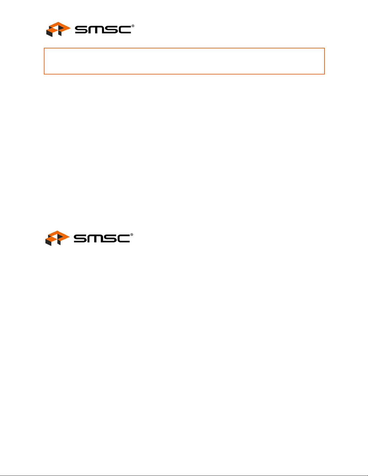
Chapter 1 General Description
The USB3500 is a stand-alone Hi-Speed USB Physical Layer Transceiver (PHY). The USB3500 uses
a UTMI+ interface to connect to an SOC or FPGA or custom ASIC. The USB3500 provides a flexible
alternative to integrating the analog PHY block for new d esigns.
SOC/FPGA/ASIC
Including Device Cont roller
Hi-Speed
USB App.
The USB3500 provides a fully compliant USB 2.0 interface, and supports High-Speed (HS), Full-Speed
(FS), and Low-Speed (LS) USB. The USB3500 supports all levels of the UTMI+ specification as shown
in Figure 1.2.
The USB3500 can also, as an option, fully support the On-the-Go (OTG) protocol defined in th e OnThe-Go Supplement to the USB 2.0 Specification. On-the-Go allows the Link to dyn amically configure
the USB3500 as host or peripheral configured dynam ically by software. For example, a cell phone may
connect to a computer as a peripheral to exchange address information or connect to a printer as a
host to print pictures. Finally the OTG enabled device can connect to another OTG enabled device to
exchange information. All this is supported using a single low profile Mini-AB USB connector.
Designs not needing OTG can ignore the OTG feature set.
UTMI+
Link
Figure 1.1 Basic UTMI+ USB Device Block Diagram
UTMI+
Interface
USB3500
UTMI+
Digital
Logic
USB 2.0
Analog
w/ OTG
V
DM
DP
BUS
ID
USB
Connector
(Standard
or Mini)
SMSC USB3500 7 Revision 1.0 (06-05-08)
DATASHEET
Hi-Speed USB Host, Device or OTG PHY With UTMI+ Interface
Datasheet
The USB3500 uses SMSC’s advanced proprietary technology to minimize power dissipation, resulting
in maximized battery life in portable applications.
UTMI+ Level 3
USB2.0 Peripheral, host controllers, On-the-
Go devices
USB3500
(HS, FS, LS, preamble packet)
UTMI+ Level 2
USB2.0 Peripheral, host controllers, On-
the-Go devices
(HS, FS, and LS but no preamble packet)
UTMI+ Level 1
USB2.0 Peripheral, host controllers, and
ADDED FEATURES
On-the-Go devices
(HS and FS Only)
1.1 Applications
The USB3500 is targeted for any application where a hi-speed USB connection is desired.
The USB3500 is well suited for:
Cell Phones
MP3 Players
Scanners
Printers
External Hard Drives
Still and Video Cameras
Portable Media Players
Entertainment Devices
UTMI+ Level 0
USB2.0 Peripherals Only
Figure 1.2 UTMI+ Level 3 Support
USB3280
USB3250
Revision 1.0 (06-05-08) 8 SMSC USB3500
DATASHEET
Hi-Speed USB Host, Device or OTG PHY With UTMI+ Interface
Datasheet
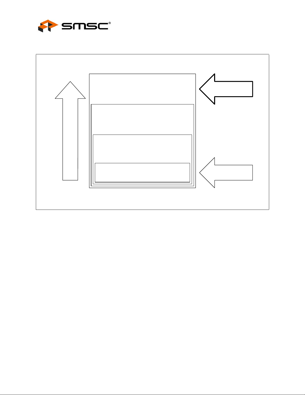
Chapter 2 Functional Overview
The USB3500 is a highly integrated USB tra nsceiver syste m. It contains a complete USB 2.0 PHY with
the UTMI+ industry standard interface to support fast time to market for a USB controller. The
USB3500 is composed of the functional blocks shown in Figure 2.1 below.
VDD3.3
XCVRSEL[1:0]
TERMSEL
TXREADY
SUSPENDN
TXVALID
RESET
CHRGVBUS
RXACTIVE
OPMODE[1:0]
ID_DIG
IDPULLUP
CLKOUT
LINESTATE[1:0]
HOSTDISC
DISCHRGVBUS
SESSEND
DATA[7:0]
RXVALID
SESSVLD
DPPD
DMPD
RXERROR
VBUSVLD
VDD1.8
VDDA1.8
Internal
Regulators
& POR
TX
Logic
RX
Logic
UTMI+
Digital
m
24 MHz
XI
XTAL
XO
XTAL &
PLL
HS XCVR
FS/LS
XCVR
USB3500
OTG
Module
Rpu_dp
Rpu_dm
Rpd_dp
Rpd_dm
Resistors
Bias
Gen.
VBUS
ID
VDD3.3
DP
DM
RBIAS
5V
Power
Supply
Mini-AB
USB
Connector
Figure 2.1 USB3500 Block Diagram
SMSC USB3500 9 Revision 1.0 (06-05-08)
DATASHEET
Hi-Speed USB Host, Device or OTG PHY With UTMI+ Interface
Chapter 3 Pin Configuration and Pin Definitions
The USB3500 is offered in a 56 pin QFN package. The pin definitions and locations are documented
below.
3.1 USB3500 Pin Locations
RBIAS
VDD3.3
VDD3.3
VDDA1.8XIXO
VSS
VDD1.8
VBUSVLD
VDD3.3
VSS
RXERROR
DMPD
DPPD
Datasheet
VSS
XCVRSEL0
TERMSEL
TXREADY
VBUS
SUSPENDN
TXVALID
RESET
VDD3.3
DP
DM
VSS
VDD3.3
56555453525150
1
2
3
4
5
6
ID
7
8
9
10
11
12
13
14
15161718192021222324252627
XCVRSEL1
CHRGVBUS
USB3500
Hi-Speed USB
UTMI+ PHY
56 Pin QFN
GND FLAG
ID_DIG
RXACTIVE
OPMODE[1]
OPMODE[0]
4847464544
49
VSS
CLKOUT
IDPULLUP
VSS
LINESTATE[1]
43
SESSVLD
42
RXVALID
41
VSS
40
DATA[0]
39
DATA[1]
38
DATA[2]
37
DATA[3]
36
DATA[4]
35
DATA[5]
34
DATA[6]
33
DATA[7]
32
SESSEND
31
DISCHRGVBUS
30
HOSTDISC
29
28
VDD1.8
VDD3.3
LINESTATE[0]
Figure 3.1 USB3500 Pinout - Top View
The flag of the QFN package must be connected to ground with a via array.
Revision 1.0 (06-05-08) 10 SMSC USB3500
DATASHEET

Hi-Speed USB Host, Device or OTG PHY With UTMI+ Interface
Datasheet
3.2 Pin Definitions
T able 3.1 USB3500 Pin Definitions
DIRECTION,
PIN NAME
1 VSS Ground N/A PHY ground.
2 XCVRSEL[0] Input N/A Transceiver Select. These signals select between
3 TERMSEL Input N/A Termination Select. This signal selects between the
4 TXREADY Output High Transmit Data Ready. If TXVALID is asserted, the
5 VBUS I/O,
6 ID Input,
TYPE
Analog
Analog
ACTIVE
LEVEL DESCRIPTION
the FS and HS transceivers:
Transceiver select.
00: HS
01: FS
10: LS
11: LS data, FS rise/fall times
FS and HS terminations:
0: HS termination enabled
1: FS termination enabled
Link must always have data available for clocking
into the TX Holding Register on the rising edge of
CLKOUT. TXREADY is an acknowledgement to the
Link that the transceiver has clocked the data from
the bus and is ready for the next transfer on the bus.
If TXVALID is negated, TXREADY can be ignored by
the Link.
N/A VBUS pin of the USB cable.
N/A ID pin of the USB cable.
7 SUSPENDN Input Low Suspend. Places the transceiver in a mode that
8TXVALID Input High Transmit Valid. Indicates that the DATA bus is valid
9 RESET Input High Rese t. Reset all state machines. After coming out
10 VDD3.3 N/A N/A 3.3V PHY Supply. Provides power for USB 2.0
11 DP I/O,
Analog
N/A D+ pin of the USB cable.
draws minimal power from supplies. In host mode,
R
is removed during suspend. In device mode,
PU
R
is controlled by TERMSEL. In suspend mode
PD
the clocks are off.
0: PHY in suspend mode
1: PHY in normal operation
for transmit. The assertion of TXVALID initiates the
transmission of SYNC on the USB bus. The
negation of TXVALID initiates EOP on the USB.
Control inputs (OPMODE[1:0],
TERMSEL,XCVERSEL) must not be changed on the
de-assertion or assertion of TXVALID.
of reset, must wait 5 rising edges of clock before
asserting TXValid for transmit.
Assertion of Reset: May be asynchronous to
CLKOUT
De-assertion of Reset: Must be synchronous to
CLKOUT
Transceiver, UTMI+ Digital, Digital I/O, and
Regulators.
SMSC USB3500 11 Revision 1.0 (06-05-08)
DATASHEET
Hi-Speed USB Host, Device or OTG PHY With UTMI+ Interface
Table 3.1 USB3500 Pin Definitions (continued)
Datasheet
DIRECTION,
PIN NAME
TYPE
12 DM I/O,
ACTIVE
LEVEL DESCRIPTION
N/A D- pin of the USB cable.
Analog
13 VSS Ground N/A PHY ground.
14 VDD3.3 N/A N/A 3.3V PHY Supply.
15
XCVRSEL[1] Input N/A Transceiver Select. These signals select between
the FS and HS transceivers:
Transceiver select.
00: HS
01: FS
10: LS
11: LS data, FS rise/fall times
16 CHRGVBUS Input High
Charge VBUS through a resistor to VDD3.3.
0: do not charge VBUS
1: charge VBUS
17 RXACTIVE Output High Receive Active. Indicates that the receive state
machine has detected Start of Packet and is active.
18 OPMODE[1] Input N/A Operatio nal Mode. These signals select between
the various operational modes:
19
OPMODE[0] Input N/A
[1] [0] Description
0 0 0: Normal Operation
0 1 1: Non-driving (all terminations removed)
1 0 2: Disable bit stuffing and NRZI encoding
1 1 3: Reserved
20 ID_DIG Output High ID Digital. Indicates the state of the ID pin .
0: connected plug is a mini-A
1: connected plug is a mini-B
21 IDPULLUP Input High
ID Pull-up. Enables sampling of the analog ID line.
Disabling the ID line sampler will reduce PHY power
consumption.
0: Disable sampling of ID line.
1: Enable sampling of ID line.
22
23
24
25
VSS Ground N/A PHY ground.
CLKOUT Output,
CMOS
N/A 60MHz reference clock output. All UTMI+ signals are
driven synchronous to this clock.
VSS Ground N/A PHY ground.
LINESTATE[1] Output N/A Line State. These signals reflect the current state of
the USB data bus in FS mode. Bit [0] reflects the
26
LINESTATE[0] Output N/A
state of DP and bit [1] reflects the state of DM. When
the device is suspended or resuming from a
suspended state, the signals are combinatorial.
Otherwise, the signals are synchronized to CLKOUT.
[1] [0] Description
0 0 0: SEO
0 1 1: J State
1 0 2: K State
1 1 3: SE1
27 VDD1.8 N/A N/A 1.8V regulator output for digital circuitry on chip.
Place a 0.1uF capacitor near this pin and connect
the capacitor from this pin to ground. Connect pin 27
to pin 49.
Revision 1.0 (06-05-08) 12 SMSC USB3500
DATASHEET
Hi-Speed USB Host, Device or OTG PHY With UTMI+ Interface
Datasheet
Table 3.1 USB3500 Pin Definitions (continued)
PIN NAME
DIRECTION,
TYPE
ACTIVE
LEVEL DESCRIPTION
28 VDD3.3 N/A N/A 3.3V PHY Supply. Provides power for USB 2.0
Transceiver, UTMI+ Digital, Digital I/O, and
Regulators.
29 HOSTDISC Output High Host Disconnect. In HS Host mode this indicates to
that a downstream device has been disconnected.
Automatically reset to 0b when Low Power Mode is
entered.
30 DISCHRGVBUS Input High Discharge VBUS through a resistor to ground.
0: do not discharge VBUS
1: discharge VBUS
31 SESSEND Output High Session End. Indicates that the vol tage on Vbus is
below its B-Device Session End threshold.
32 DATA[7] I/O,
CMOS,
0: VBUS > V
1: VBUS < V
N/A 8-bit bi-directional data bus. Data[7] is the MSB and
Data[0] is the LSB.
SessEnd
SessEnd
Pull-low
33
DATA[6] I/O,
N/A
CMOS,
Pull-low
34
DATA[5] I/O,
N/A
CMOS,
Pull-low
35
DATA[4] I/O,
N/A
CMOS,
Pull-low
36
DATA[3] I/O,
N/A
CMOS,
Pull-low
37
DATA[2] I/O,
N/A
CMOS,
Pull-low
38
DATA[1] I/O,
N/A
CMOS,
Pull-low
39
DATA[0] I/O,
N/A
CMOS,
Pull-low
40
VSS Ground N/A PHY ground.
41 RXVALID Output High Receive Data Valid. Indicates that the DATA bus has
received valid data. The Receive Data Holding
Register is full and ready to be unloaded. The Link
is expected to register the DATA bus on the next
rising edge of CLKOUT.
42 SESSVLD Output High Session Valid. Indicates that the voltage on Vbus is
above the indicated threshold.
0: VBUS < V
1: VBUS > V
SessVld
SessVld
SMSC USB3500 13 Revision 1.0 (06-05-08)
DATASHEET

Hi-Speed USB Host, Device or OTG PHY With UTMI+ Interface
Table 3.1 USB3500 Pin Definitions (continued)
Datasheet
PIN NAME
DIRECTION,
TYPE
ACTIVE
LEVEL DESCRIPTION
43 DPPD Input N/A DP Pull-down Sele ct. This signal enables the 15k
Ohm pull-down resistor on the DP line.
0: Pull-down resistor not connected to DP
1: Pull-down resistor connected to DP
44
DMPD Input N/A DM Pull-down Sele ct. This signal enables the 15k
Ohm pull-down resistor on the DM line.
0: Pull-down resistor not connected to DM
1: Pull-down resistor connected to DM
45 RXERROR Output High Receive Error. This output is clocked with the same
timing as the receive DATA lines and can occur at
anytime during a transfer.
0: Indicates no error.
1: Indicates a receive error has been detected.
46 VSS Ground N/A PHY ground.
47 VBUSVLD Output High VBUS Valid. Indicates that the voltage on Vbus is
above the indicated threshold.
0: VBUS < V
1: VBUS > V
VbusVld
VbusVld
48 VDD3.3 N/A N/A 3.3V PHY Supply. Provides power for USB 2.0
Transceiver, UTMI+ Digital, Digital I/O, and
Regulators.
49 VDD1.8 N/A N/A 1.8V regulator output for digital circuitry on chip.
Place a 4.7uF low ESR capacitor near this pin and
connect the capacitor from this pin to ground.
Connect pin 49 to pin 27. See Section 6.6, "Internal
Regulators and POR," on page 27.
50 VSS Ground N/A PHY ground.
51
52
XO Output,
Analog
XI Input,
Analog
N/A Crystal pin. If using an external clock on XI this pin
should be floated.
N/A Crystal pin. A 24MHz crystal is supported. The
crystal is placed across XI and XO. An external
24MHz clock source may be driven into XI in place
of a crystal.
53 VDDA1.8 N/A N/A 1.8V regulator output for analog circuitry on chip.
Place a 0.1uF capacitor near this pin and connect
the capacitor from this pin to ground. In parallel,
place a 4.7uF low ESR capacitor near this pin and
connect the capacitor from this pin to ground. See
Section 6.6, "Internal Regulators and POR".
54 VDD3.3 N/A N/A 3.3V PHY Supply. Provides power for USB 2.0
Transceiver, UTMI+ Digital, Digital I/O, and
Regulators.
55 VDD3.3 N/A N/A 3.3V PHY Supply. Should be connected directly to
pin 54.
56
RBIAS Analog,
CMOS
N/A External 1% bias resistor. Requires a 12KΩ resistor
to ground.
GND FLAG Ground N/A Ground. The flag must be connecte d to the ground
plane.
Revision 1.0 (06-05-08) 14 SMSC USB3500
DATASHEET
Hi-Speed USB Host, Device or OTG PHY With UTMI+ Interface
Datasheet
Chapter 4 Limiting Values
Table 4.1 Maximum Guaranteed Ratings
PARAMETER SYMBOL CONDITIONS MIN TYP MAX UNITS
Maximum VBUS, ID, DP,
and DM voltage to
Ground
Maximum VDD1.8 and
VDDA1.8 voltage to
Ground
Maximum 3.3V supply
voltage to Ground
Maximum I/O voltage to
Ground
Operating Temperature T
Storage Temperature T
Note: Stresses above those listed could cause damage to the device. This is a stress rating on ly and
functional operation of the device at any other condition above those indicated in the operation
sections of this specification is not implied. When powering this device from laboratory or
system power supplies, it is important that the Absolute Maximum Ratings not be exceeded or
device failure can result. Some power supplies exhibit voltage spikes on their outputs when the
AC power is switched on or off. In addition, voltage transients on the AC power line may appear
on the DC output. If this possibility exists, it is suggested that a clamp circuit be used.
V
MAX_5V
V
MAX_1.8V
V
MAX_3.3V
V
MAX_IN
MAX_OP
MAX_STG
Table 4.2 Recommended Operating Conditions
-0.5 +5.5 V
-0.5 2.5 V
-0.5 4.0 V
-0.5 4.0 V
070C
-55 150 C
PARAMETER SYMBOL CONDITIONS MIN TYP MAX UNITS
3.3V Supply Voltage V
Input Voltage on Digital Pins V
Input Voltage on Analog I/O
Pins (DP, DM)
Ambient Temperature T
DD3.3
I
V
I(I/O)
A
3.0 3.3 3.6 V
0.0 V
0.0 V
DD3.3
DD3.3
0+70
V
V
o
C
Table 4.3 Recommended Externa l Cl ock Conditions
PARAMETER SYMBOL CONDITIONS MIN TYP MAX UNITS
System Clock Frequency XI driven by the external clock;
and no connection at XO
System Clock Duty Cycle XI driven by the external clock;
45 50 55 %
(±
100ppm)
24
MHz
and no connection at XO
SMSC USB3500 15 Revision 1.0 (06-05-08)
DATASHEET
Hi-Speed USB Host, Device or OTG PHY With UTMI+ Interface
Chapter 5 Electrical Characteristics
T able 5.1 DC Electrical Characteristics: Supply Pins (Note 1)
PARAMETER SYMBOL CONDITIONS MIN TYP MAX UNITS
Datasheet
Unconfigured Current I
FS Idle Current I
FS Transmit Current I
FS Receive Current I
HS Idle Current I
HS Transmit Current I
HS Receive Current I
Low Power Mode I
Note: V
= 3.0 to 3.6V; VSS = 0V; TA = 0C to +70C; unless otherwise specified.
DD3.3
Table 5.2 Electrical Characteristics: CLKOUT Start-Up
PARAMETER SYMBOL CONDITIONS MIN TYP MAX UNITS
AVG(UCFG)
AVG(FS)
AVG(FSTX)
AVG(FSRX)
AVG(HS)
AVG(HSTX)
AVG(HSRX)
DD(LPM)
Device Unconfigured 55 mA
FS idle not data transfer 55 mA
FS current during data
60.5 mA
transmit
FS current during data
57.5 mA
receive
FS idle not data transfer 60.6 mA
FS current during data
62.4 mA
transmit
FS current during data
61.5 mA
receive
VBUS 15kΩ pull-down and
83 uA
1.5kΩ pull-up resistor
currents not included.
Suspend Recovery Time T
Note: V
= 3.0 to 3.6V; VSS = 0V; TA = 0C to +70C; unless otherwise specified.
DD3.3
START
2.25 3.5 ms
T able 5.3 DC Electrical Characteristics: Logic Pins
PARAMETER SYMBOL CONDITIONS MIN TYP MAX UNITS
Low-Level Input Voltage V
High-Level Input Voltage V
Low-Level Output Voltage V
High-Level Output Voltage V
Input Leakage Current I
IL
IH
OL
OH
LI
IOL = 8mA 0.4 V
IOH = -8mA V
V
SS
2.0 V
DD3.3
- 0.4
0.8 V
DD3.3
V
V
±10 uA
Pin Capacitance Cpin 4 pF
Note: V
Revision 1.0 (06-05-08) 16 SMSC USB3500
= 3.0 to 3.6V; VSS = 0V; TA = 0C to +70C; unless otherwise specified.
DD3.3
DATASHEET

Hi-Speed USB Host, Device or OTG PHY With UTMI+ Interface
Datasheet
T able 5.4 DC Electrical Characteristics: Analog I/O Pins (DP/DM)
PARAMETER SYMBOL CONDITIONS MIN TYP MAX UNITS
FS FUNCTIONALITY
Input levels
Differential Receiver Input
Sensitivity
Differential Receiver
Common-Mode Voltage
Single-Ended Receiver Low
Level Input Voltage
Single-Ended Receiver High
Level Input Voltage
Single-Ended Receiver
Hysteresis
Output Levels
Low Level Output Voltage V
High Level Output Voltage V
T ermination
Driver Output Impedance for
HS and FS
Input Impedance Z
Pull-up Resistor Impedance Z
Pull-up Resistor Impedance Z
Pull-dn Resistor Impedance Z
HS FUNCTIONALITY
V
DIFS
V
CMFS
V
ILSE
V
IHSE
V
HYSSE
FSOL
FSOH
Z
HSDRV
INP
PU
PURX
PD
| V(DP) - V(DM) | 0.2 V
0.8 2.5 V
0.8 V
2.0 V
0.050 0.150 V
Pull-up resistor on DP;
RL = 1.5kΩ to V
DD3.3
Pull-down resistor on DP,
2.8 3.6 V
0.3 V
DM;
RL = 15kΩ to GND
Steady state drive 40.5 45 49.5 Ω
TX, RPU disabled 1.0 MΩ
Bus Idle 0.900 1.24 1.575 kΩ
Device Receiving 1.425 2.26 3.09 kΩ
14.25 15.0 15.75 kΩ
Input levels
HS Differential Input
Sensitivity
HS Data Signaling Common
Mode Voltage Range
HS Squelch Detection
Threshold (Differential) V
V
DIHS
V
CMHS
HSSQ
| V(DP) - V(DM) | 100 mV
-50 500 mV
Squelch Threshold 100 mV
Un-squelch Threshold 150 mV
Output Levels
Hi-Speed Low Level
Output Voltage (DP/DM
V
HSOL
45Ω load -10 10 mV
referenced to GND)
SMSC USB3500 17 Revision 1.0 (06-05-08)
DATASHEET
Hi-Speed USB Host, Device or OTG PHY With UTMI+ Interface
Datasheet
Table 5.4 DC Electrical Characteristics: Analog I/O Pins (DP/DM) (continued)
PARAMETER SYMBOL CONDITIONS MIN TYP MAX UNITS
Hi-Speed High Level
Output Voltage (DP/DM
referenced to GND)
Hi-Speed IDLE Level
Output Voltage (DP/DM
referenced to GND)
Chirp-J Output Voltage
(Differential)
Chirp-K Output Voltage
(Differential)
Leakage Current
OFF-State Leakage Current I
Port Capacitance
Transceiver Input
Capacitance
Note: V
= 3.0 to 3.6V; VSS = 0V; TA = 0C to +70C; unless otherwise specified.
DD3.3
T able 5.5 Dynamic Characteristics: Analog I/O Pins (DP/DM)
V
HSOH
V
OLHS
V
CHIRPJ
V
CHIRPK
LZ
C
IN
45Ω load 360 440 mV
45Ω load -10 10 mV
HS termination resistor
700 1100 mV
disabled, pull-up resistor
connected. 45Ω load.
HS termination resistor
-900 -500 mV
disabled, pull-up resistor
connected. 45Ω load.
±10 uA
Pin to GND 5 10 pF
PARAMETER SYMBOL CONDITIONS MIN TYP MAX UNITS
FS Output Driver Timing
Rise Time T
Fall Time T
Output Signal Crossover
Voltage
Differential Rise/Fall Time
Matching
FSR
FFF
V
CRS
FRFM Excluding the first
CL = 50pF; 10 to 90% of
|VOH - VOL|
CL = 50pF; 10 to 90% of
|VOH - VOL|
Excluding the first
transition from IDLE state
transition from IDLE state
420ns
420ns
1.3 2.0 V
90 111.1 %
HS Output Driver Timing
Differential Rise Time T
Differential Fall Time T
Driver Waveform
Requirements
HSR
HSF
Eye pattern of Template 1
in USB 2.0 specification
500 ps
500 ps
Hi-Speed Mode Timing
Receiver Waveform
Requirements
Data Source Jitter and
Receiver Jitter Tolerance
Eye pattern of Template 4
in USB 2.0 specification
Eye pattern of Template 4
in USB 2.0 specification
Revision 1.0 (06-05-08) 18 SMSC USB3500
DATASHEET

Hi-Speed USB Host, Device or OTG PHY With UTMI+ Interface
Datasheet
Note: V
= 3.0 to 3.6V; VSS = 0V; TA = 0C to +70C; unless otherwise specified.
DD3.3
T able 5.6 Dynamic Characteristics: Digital UTMI Pins
PARAMETER SYMBOL CONDITIONS MIN TYP MAX UNITS
UTMI Timing
DATA[7:0] T
RXVALID
RXACTIVE
RXERROR
LINESTATE[1:0]
TXREADY
DATA[7:0] T
TXVALID
OPMODE[1:0]
XCVRSELECT[1:0]
TERMSELECT
DATA[7:0] T
TXVALID
OPMODE[1:0]
XCVRSELECT[1:0]
TERMSELECT
PD
SU
H
Output Delay. Measured
from PHY output to the
rising edge of CLKOUT
Setup Time. Measured
from PHY input to the
rising edge of CLKOUT.
Hold time. Measured from
the rising edge of
CLKOUT to the PHY input
signal edge.
25ns
51ns
0ns
Note: V
= 3.0 to 3.6V; VSS = 0V; TA = 0C to +70C; unless otherwise specified.
DD3.3
Table 5.7 OTG Electrical Characteristics
PARAMETER SYMBOL CONDITIONS MIN TYP MAX UNITS
SessEnd trip point V
SessVld trip point V
VBUSVld trip point V
Vbus Pull-Up R
Vbus Pull-down R
Vbus Impedance R
ID pull-up resistance R
ID pull-up resistance R
SMSC USB3500 19 Revision 1.0 (06-05-08)
SessEnd
SessVld
VbusVld
VbusPu
VbusPd
Vbus
IdPullUp
Id
Vbus to VDD3.3
(CHRGVBUS = 1)
Vbus to GND
(DISCHRGVBUS = 1)
Vbus to GND 40 75 100 kΩ
(IDOULLUP = 1) 80 100 120 k Ω
(IDPULLUP = 0) 1 MΩ
0.2 0.5 0.8 V
0.8 1.4 2.0 V
4.4 4.58 4.75 V
281 340 Ω
656 850 Ω
DATASHEET
Hi-Speed USB Host, Device or OTG PHY With UTMI+ Interface
Datasheet
Note: V
= 3.0 to 3.6V; VSS = 0V; TA = 0C to +70C; unless otherwise specified
DD3.3
Table 5.8 Regulator Output Voltages
PARAMETER SYMBOL CONDITIONS MIN TYP MAX UNITS
V
DDA1.8
V
DDA1.8
V
DD1.8
Note: V
DD3.3
V
DDA1.8
V
DDA1.8
V
DD1.8
Normal Operation
(SUSPENDN = 1)
Low Power mode
(SUSPENDN = 0)
1.6 1.8 2.0 V
0V
1.6 1.8 2.0 V
= 3.0 to 3.6V; VSS = 0V; TA = 0C to +70C; unless otherwise specified
Revision 1.0 (06-05-08) 20 SMSC USB3500
DATASHEET
Hi-Speed USB Host, Device or OTG PHY With UTMI+ Interface
Datasheet
Chapter 6 Detailed Functional Description
Figure 2.1 on page 9 shows the functional block diagram of the USB3500. Each of the functions is
described in detail below.
6.1 8bit Bi-Directional Data Bus Operation
The USB3500 supports an 8-bit bi-directional parallel interface.
CLKOUT runs at 60MHz
The 8-bit data bus (DATA[7:0]) is used for transmit when TXVALID = 1
The 8-bit data bus (DATA[7:0]) is used for receive when TXVALID = 0
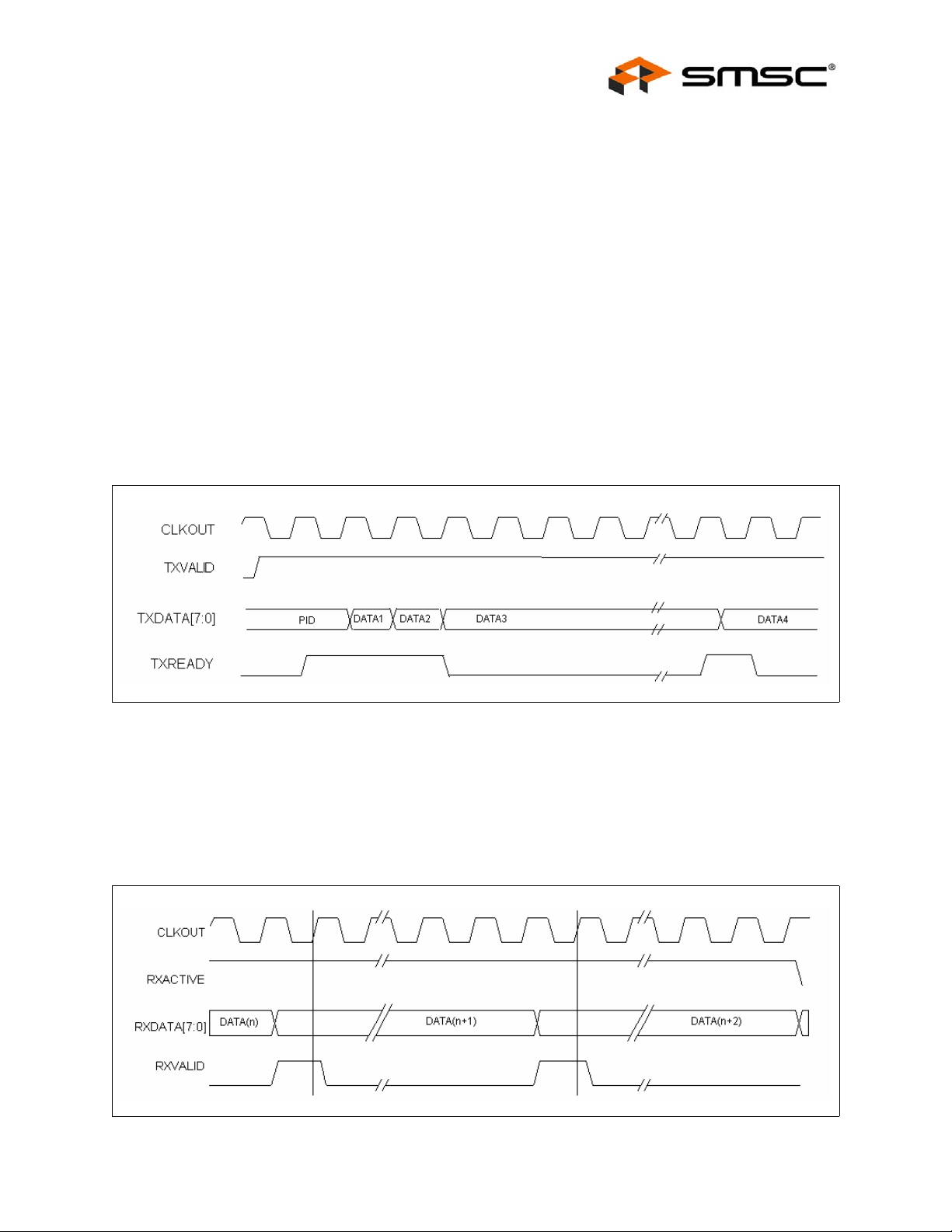
Figure 6.1 shows the relationship between CLKOUT and the transmit data transfer signals in FS mode.
TXREADY is only asserted for one CLKOUT per byte time to signal the Link that the d ata on the DATA
lines has been read by the PHY. The Link may hold the data on the DATA lines for the duration of the
byte time. Transitions of TXVALID must meet the defined setup and hold times relative to CLKOUT.
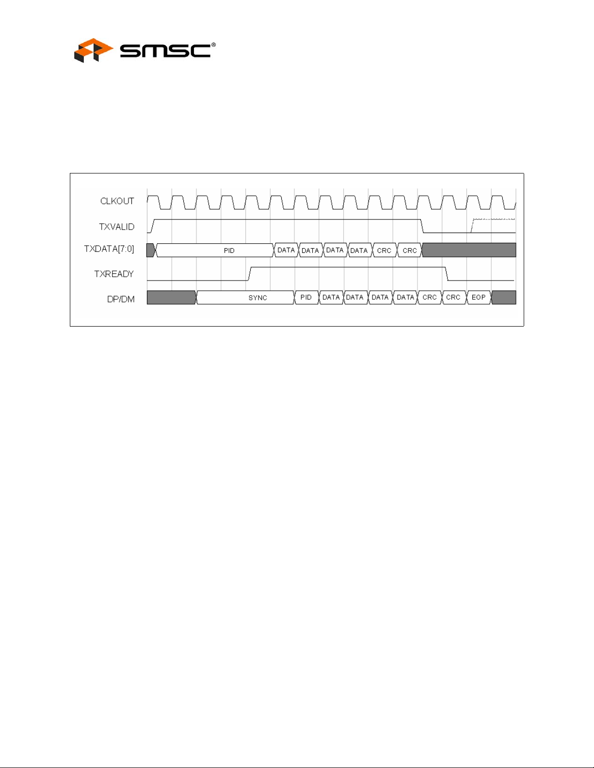
Figure 6.1 FS CLK Relationship to Transmit Data and Control Signals
Figure 6.2 shows the relationship between CLKOUT and the receive data control signals in FS mode.
RXACTIVE “frames” a packet, transitioning only at the beginning and end of a packet. However
transitions of RXVALID may take place any time 8 bits of data are available. Figure 6.2 also shows
how RXVALID is only asserted for one CLKOUT cycle per byte time even though the data may be
presented for the full byte time. The XCVRSELECT signal determines whether the HS or F S timing
relationship is applied to the data and control signals.
Figure 6.2 FS CLK Relationship to Receive Data and Control Signals
SMSC USB3500 21 Revision 1.0 (06-05-08)
DATASHEET
6.2 TX Logic
This block receives parallel data bytes placed on the DATA bus and performs the necessary transmit
operations. These operations include parallel to serial conversion, bit stuffing and NRZI encoding.
Upon valid assertion of the proper TX control lines by the Link and T X State Machine, the TX LOGIC
block will synchronously shift, at either the FS or HS rate, the data to the FS/HS TX block to be
transmitted on the USB cable. Data transmit timing is shown in Figure 6.3.
Hi-Speed USB Host, Device or OTG PHY With UTMI+ Interface
Datasheet
Figure 6.3 Transmit Timing for a Data Packet
The behavior of the Transmit State Machine is described below.
The Link asserts TXVALID to begin a transmission.
After the Link asserts TXVALID it can assume that the transmission has started when it detects
TXREADY has been asserted.
The Link must assume that the USB3500 has consumed a data byte if TXREADY and TXVALID
are asserted on the rising edge of CLKOUT.
The Link must have valid packet information (PID) asserted on the DATA bus coincident with the
assertion of TXVALID.
TXREADY is sampled by the Link on the rising edge of CLKOUT.
The Link negates TXVALID to complete a packet. Once negated, the transmit logic will never
reassert TXREADY until after the EOP has been generated. (TXREADY will not re-assert until
TXVALD asserts again.)
The USB3500 is ready to transmit another packet immediately. However, the Link must conform to
the minimum inter-packet delays identified in the USB 2.0 specification.
Supports high speed disconnect detect through the HOSTDISC pin. In Host mode the USB3500
will sample the disconnect comparator at the 32nd bit of the 40 bit l ong EOP during SOF packets.
Supports FS pre-amble for FS hubs with a LS device.
Supports LS keep alive by receiving the SOF PID.
Supports Host mode resume K which ends with two low speed times of SE0 followed by 1 FS “J”.
6.3 RX Logic
This block receives serial data from the clock recovery circuits and processes it to b e transferred to
the Link on the DATA bus. The processing involved includes NRZI decoding, bit unstuffing, and serial
to parallel conversion. Upon valid assertion of the proper RX control lines, the RX Logic block will
provide bytes to the DATA bus as shown in the figures below. The behavior of the receiver is describ ed
below.
Revision 1.0 (06-05-08) 22 SMSC USB3500
DATASHEET

Hi-Speed USB Host, Device or OTG PHY With UTMI+ Interface
Datasheet
Figure 6.4 Receive Timing for Data with Unstuffed Bits
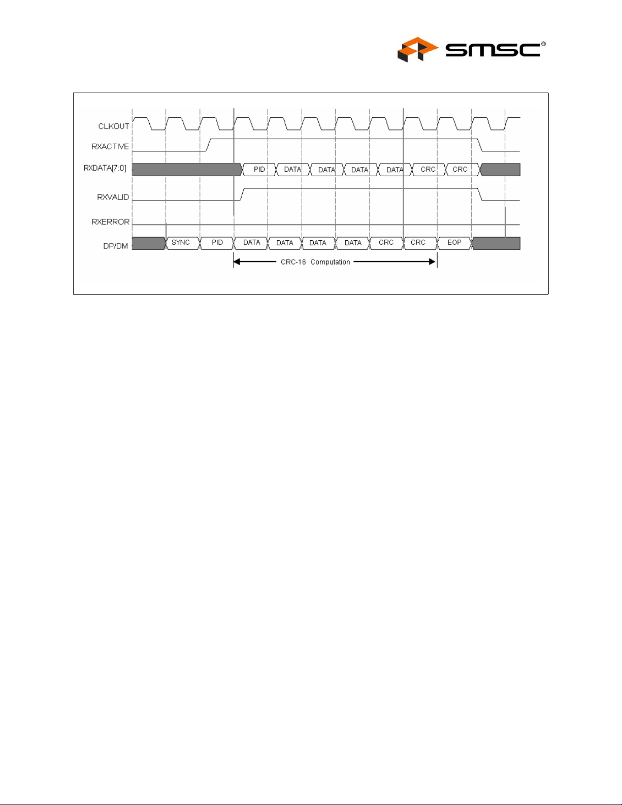
The assertion of RESET will cause the USB3500 to deasserts RXACTIVE and RXVALID. When the
RESET signal is deasserted the Receive State Machine starts looking for a SYNC pattern on the USB.
When a SYNC pattern is detected, the receiver will assert RXACTIVE. The length of the received HiSpeed SYNC pattern varies and can be up to 32 bits long or as short as 12 bits long when at the end
of five hubs.
After valid serial data is received, the data is loaded into the RX Holding Register on the rising edge
of CLKOUT, and RXVALID is asserted. The Link must read the DATA bus on the next rising edge of
CLKOUT. In normal mode (OPMODE = 00), then stuffed bits are stripped from the data stream. Each
time 8 stuffed bits are accumulated the USB3500 will negate RXVALID for one clock cycle, thus
skipping a byte time.
When the EOP is detected the USB3500 will negate RXACTIVE and RXVALID. After the EOP has
been stripped, the USB3500 will begin looking for th e next packet.
The behavior of the USB3500 receiver is described below:
RXACTIVE and RXREADY are sampled on the rising edge of CLKOUT.
After a EOP is complete the receiver will begin looking for SYNC.
The USB3500 asserts RXACTIVE when SYNC is detected.
The USB3500 negates RXACTIVE when an EOP is detected and the elasticity buffer is empty.
When RXACTIVE is asserted, RXVALID will be asserted if the RX Holding Register is full.
RXVALID will be negated if the RX Holding Register was not loaded during the previous byte time.
This will occur if 8 stuffed bits have been accumulated.
The Link must be ready to consume a data byte if RXACTIVE and RXVALID are asserted (RX Data
state).
Figure 6.5 shows the timing relationship between the received data (DP/DM), RXVALID,
RXACTIVE, RXERROR and DATA signals.
Notes:
Figure 6.5, Figure 6.6 and Figure 6.7 are timi ng examples of a HS/FS PHY when it is in HS mode.
When a HS/FS PHY is in FS Mode there are approximately 40 CLKOUT cycles every byte time.
The Receive State Machine assumes that the Link captures the data on the DATA bus if RXACTIVE
and RXVALID are asserted. In FS mode, RXVALID will only be asserted for one CLKOUT per byte
time.
In Figure 6.5, Figure 6.6 and Figure 6.7 the SYNC pattern on DP/DM is shown as one byte long.
The SYNC pattern received by a device can vary in length. These figures assume that all but the
last 12 bits have been consumed by the hubs between the device and the host controller.
SMSC USB3500 23 Revision 1.0 (06-05-08)
DATASHEET
Hi-Speed USB Host, Device or OTG PHY With UTMI+ Interface
Figure 6.5 Receive Timing for a Handshake Packet (no CRC)
Datasheet
Figure 6.6 Receive Timing for Setup Packet
Revision 1.0 (06-05-08) 24 SMSC USB3500
DATASHEET
Hi-Speed USB Host, Device or OTG PHY With UTMI+ Interface
Datasheet
Figure 6.7 Receive Timing for Data Packet (with CRC-16)
6.4 USB 2.0 Transceiver
The SMSC Hi-Speed USB 2.0 Transceiver consists of four blocks in the lower left corner of Figure 2.1
on page 9. These four blocks are labeled HS XCVR, FS/LS XCVR, Resistors, and Bias Gen.
6.4.1 High Speed and Full Speed Transceivers
The USB3500 transceiver meets all requirements in the USB 2.0 specification.
The receivers connect directly to the USB cable. This block contains a separate differential receiver
for HS and FS mode. Depending on the mode, the selected receiver provides the serial data stream
through the multiplexer to the RX Logic block. The FS mode section of the FS/HS RX block also
consists of a single-ended receiver on each of the data lines to determine the correct FS linestate. For
HS mode support, the FS/HS RX block contains a squelch circuit to insure that noise is never
interpreted as data.
The transmitters connect directly to the USB cable. The block contains a separate differential FS and
HS transmitter which receive encoded, bit stuffed, serialized data from the TX Logic block and transmit
it on the USB cable.
6.4.2 Termination Resistors
The USB3500 transceiver fully integrates all of the USB termination resistors. The USB3500 includes
two 1.5kΩ pull-up resistors on DP and DM and a 15kΩ pull-down resistor on both DP and DM. In
addition the 45Ω high speed termination resistors are also integrated. These integrated resistors
require no tuning or trimming by the Link. The state of the resistors is determined by the operating
mode of the PHY. The possible valid resistor combinations are shown in Table 6.1. The RESISTOR
SETTINGS signals shown in the table are internal to the USB3500.
RPU_DP_EN activates the 1.5kΩ DP pull-up resistor
RPU_DM_EN activates the 1.5kΩ DM pull-up resistor
RPD_DP_EN activates the 15kΩ DP pull-down resistor
RPD_DM_EN activates the 15kΩ DM pull-down resistor
SMSC USB3500 25 Revision 1.0 (06-05-08)
DATASHEET

Hi-Speed USB Host, Device or OTG PHY With UTMI+ Interface
Datasheet
HSTERM_EN activates the 45Ω DP and DM high speed termination resistors
Table 6.1 DP/DM termination vs. Signaling Mode
UTMI+ INTERFACE SETTINGS RESISTOR SETTINGS
DPPD
SIGNALING MODE
TERMSEL
XCVRSEL[1:0]
OPMODE[1:0]
General Settings
Tri-State Drivers XXb Xb 01b Xb Xb 0b 0b 0b 0b 0b
DMPD
RPU_DM_EN
RPD_DP_EN
RPD_DM_EN
RPU_DP_EN
HSTERM_EN
Power-up or Vbus < V
SESSEND
01b 0b 00b 1b 1b 0b 0b 1b 1b 0b
Host Settings
Host Chirp 00b 0b 10b 1b 1b 0 b 0b 1b 1b 1b
Host Hi-Speed 00b 0b 00b 1b 1b 0b 0b 1b 1b 1b
Host Full Speed X1b 1b 00b 1b 1b 0b 0b 1b 1b 0b
Host HS/FS Suspend 01b 1b 00b 1b 1b 0b 0b 1b 1b 0b
Host HS/FS Resume 01b 1b 10b 1b 1b 0b 0b 1b 1b 0b
Host low Speed 10b 1b 00b 1b 1b 0b 0b 1b 1b 0b
Host LS Suspend 10b 1b 00b 1b 1b 0b 0b 1b 1b 0b
Host LS Resume 10b 1b 10b 1b 1b 0b 0b 1b 1b 0b
Host Test J/Test_K 00b 0b 10b 1b 1b 0b 0b 1b 1b 1b
Peripheral Settings
Peripheral Chirp 00b 1b 10b 0b 0b 1b 0b 0b 0b 0b
Peripheral HS 00b 0b 00b 0b 0b 0b 0b 0b 0b 1b
Peripheral FS 01b 1b 00b 0b 0b 1b 0b 0b 0b 0b
Peripheral HS/FS Suspend 01b 1b 00b 0b 0b 1b 0b 0b 0b 0b
Peripheral HS/FS Resume 01b 1b 10b 0b 0b 1b 0b 0b 0b 0b
Peripheral LS 10b 1b 00b 0b 0b 0b 1b 0b 0b 0b
Peripheral LS Suspend 10b 1b 00b 0b 0b 0b 1b 0b 0b 0b
Peripheral LS Resume 10b 1b 10b 0b 0b 0b 1b 0b 0b 0b
Peripheral Test J/Test K 00b 0b 10b 0b 0b 0b 0b 0b 0b 1b
OTG device, Peripheral Chirp 00b 1b 10b 0b 1b 1b 0b 0b 1b 0b
OTG device, Peripheral HS 00b 0b 00b 0b 1b 0b 0b 0b 1b 1b
OTG device, Peripheral FS 01b 1b 00b 0b 1 b 1b 0b 0b 1b 0b
OTG device, Peripheral HS/FS Suspend 01b 1b 00b 0b 1b 1b 0b 0b 1b 0b
Revision 1.0 (06-05-08) 26 SMSC USB3500
DATASHEET
Hi-Speed USB Host, Device or OTG PHY With UTMI+ Interface
Datasheet
Table 6.1 DP/DM termination vs. Signaling Mode (continued)
UTMI+ INTERFACE SETTINGS RESISTOR SETTINGS
DPPD
SIGNALING MODE
OTG device, Peripheral HS/FS Resume 01b 1b 10b 0b 1b 1b 0b 0b 1b 0b
OTG device, Peripheral Test J/Test K 00b 0b 10b 0b 1b 0b 0b 0b 1b 1b
TERMSEL
XCVRSEL[1:0]
OPMODE[1:0]
DMPD
RPU_DP_EN
RPD_DP_EN
RPU_DM_EN
RPD_DM_EN
6.4.3 Bias Generator
This block consists of an internal bandgap reference circuit used fo r generating the high speed driver
currents and the biasing of the analog circuits. This block requires an external 12KΩ, 1% tolerance,
external reference resistor connected from RBIAS to ground.
6.5 Crystal Oscillator and PLL
HSTERM_EN
The USB3500 uses an internal crystal driver and PLL sub-system to provide a clean 480MHz reference
clock that is used by the PHY during both transmit and receive. The USB350 0 requires a clean 24MHz
crystal or clock as a frequency reference. If the 24MHz reference is noisy or off frequency the PHY
may not operate correctly.
The USB3500 can use either a crystal or an external clock oscillator for the 24MHz reference. The
crystal is connected to the XI and XO pins as shown in the application diagram, Figure 7.10. If a clock
oscillator is used, the clock should be connected to the XI input and the XO pin left floating. When
using an external clock, the clock source must be clean so it does not degrade performance, and
should be be driven with a 0 to 3.3 volt signal.
After the 480MHz PLL has locked to the correct frequency, it will drive the CLKOUT pin with a 60MHz
clock. The USB3500 is guaranteed to start the clock within the time specified in Table 5.2.
6.6 Internal Regulators and POR
The USB3500 includes integrated power management functions to reduce the bill of materials and
simplify product design.
6.6.1 Internal Regulators
The USB3500 has two internal regulators that create tw o 1.8V outputs (labeled VDD1.8 and VDDA1.8)
from the 3.3 volt power supply input (VDD3.3). Each regulator requires an external 4.7uF +/-20% low
ESR bypass capacitor to ensure stability. X5R or X7R ceramic capacitors are recommended since they
exhibit an ESR lower that 0.1ohm at frequencies greater than 1 0kHz.
The specific capacitor recommendations for each pin are detailed in Table 3.1, "USB3500 Pin
Locations", and shown in Figure 7.10, "USB3500 Application Diagram (Top View)".
Note: The USB3500 regulators are designed to generate a 1.8volt supply for the USB3500 only.
Using the regulators to provide current for other circuits is not recommended and SMSC does
not guarantee USB performance or regulator stability in this case.
SMSC USB3500 27 Revision 1.0 (06-05-08)
DATASHEET

Hi-Speed USB Host, Device or OTG PHY With UTMI+ Interface
6.6.2 Power On Reset (POR)
The USB3500 provides an internal POR circuit that generates a reset pulse once the PHY supplies
are stable. The UTMI+ Digital can be reset at any time with the RESET pin.
6.7 USB On-The-Go (OTG) Module
The USB3500 provides support for USB OTG. This mode allows the USB3500 to be dynamically
configured as a host or a device depending on the type of cable inserted into the Mini-AB connector.
When the Mini-A plug of a cable is inserted into the Mini-AB connector the USB device becomes the
A-device. When a Mini-B plug is inserted the device becomes the B-device. The OTG A-device
behaves similar to a Host while the B-device behaves similar to a peripheral. The differences are
covered in the OTG supplement.
The OTG Module meets all the requirements in the “On-The-Go Supplement to the USB 2.0
Specification”. In applications where only Host or Device is required, the OTG Module is unused.
VDD33
Datasheet
IDPULLUP
VBUS
R>1M
ID
R=75K
R>=656 R>=281
R=100K
0.5V
1.4V
4.575V
0.6V
ID_DIG
SESSEND
CHRGVBUS
SESSVLD
VBUSVLD
DISCHRGVBUS
OTG Module
Figure 6.8 USB3500 On-the-Go Module
The OTG Module can be broken into 4 main blocks; ID Detection, VBUS Control, Driving External
VBUS, and External VBUS Detection. Each of these blocks is covered in the sections below.
Revision 1.0 (06-05-08) 28 SMSC USB3500
DATASHEET
Hi-Speed USB Host, Device or OTG PHY With UTMI+ Interface
Datasheet
6.7.1 ID Detection
The USB3500 provides an ID pin to determine the type of USB cab le connected. When the Mini-A
Plug of a USB cable is inserted into the Mini-AB connector, the ID pin is shorted to ground. When the
Mini-B Plug is inserted into the Mini-AB connector, the ID pin is allowed to float.
Table 6.2 IdGnd vs. USB Cable Type
USB PLUG OTG ROLE ID VOLTAGE IDGND
AHOST0 0
B PERIPHERAL 3.3 1
The USB3500 provides an integrated pull-up resistor to pull the ID pin to VDD3.3 when a Mini-B plug
is inserted and the cable is floating. When a Mini-A plug is connected, the pull-up resistor will be
overpowered and the ID pin will be brought to ground. To save current when a Mini-A Plug is inserted,
the ID pull-up resistor can be disabled by clearing the IDPULLUP pin. To prevent the ID pin from
floating to a random value, a weak pull-up resistor is provided at all times. The circuits related to the
ID comparator are shown in Figure 6.8 and their related parameters are shown in Table 5.7.
6.7.2 VBUS Control
The USB3500 includes all of the Vbus comparators required for OTG. The VbusVld, SessVld, and
SessEnd comparators are fully integrated into the USB3500. These comparators are used to en sure
the Vbus voltage is the correct value for proper USB operation.
The VbusVld comparator is used by the Link, when configured as an A device, to ensu re that the Vbus
voltage on the cable is valid. The SessVld comparator is used by the Link when configured as either
an A or B device to indicate a session is requested or valid. Fina lly the SessEnd comparator is used
by the B-device to indicate a USB session has ended.
Also included in the VBUS Control block are the resistors used for VBUS pulsing in SRP. The resistors
used for VBUS pulsing include a pull-down to groun d and a pull-up to VDD3.3.
6.7.2.1 SessEnd Comparator
The SessEnd comparator is designed to trip when Vbus is less than 0.5 volts. When Vbus goes below
0.5 volts, the session is considered to be ended and SessEnd will transition from 0 to 1. The SessEnd
comparator is disabled when the Suspendn = 0. When disabled, the SessEnd output is 0. The
SessEnd comparator trip points are detailed in Table 5.7.
6.7.2.2 SessVld Comparator
The SessVld comparator is used when the PHY is configured as either an A or B device. When
configured as an A device, the SessVld is used to detect Session Request protocol (SRP). When
configured as a B device, SessVld is used to detect the presence of Vbus. The SessVld comparator
is not disabled with Suspendn and its output will always reflect the state of VBUS. The SessVld
comparator trip point is detailed in Table 5.7.
Note: The OTG Supplement specifies a voltage range for A-Device Session Valid and B-Device
Session Valid comparator. The USB3500 PHY combines the two comparators into one and
uses the narrower threshold range.
6.7.2.3 VbusVld Comparator
The final Vbus comparator is the VbusVld comparator. This comparator is only used when configured
as an A-device. In the OTG protocol the A-device is responsible to ensure that the VBUS voltage is
within a certain range. The VbusVld comparator is disabled when Suspendn = 0. When disabled the
VbusVld will read 0. The VbusVld comparator trip points are detailed in Table 5.7.
SMSC USB3500 29 Revision 1.0 (06-05-08)
DATASHEET

When the A-device is able to provide 8-100mA, it must ensure Vbus doesn’t go below 4.4 volts. If the
A-device can provide 100-500mA on VBUS, it must ensure that Vbus does not go below 4.75 volts.
The internal Vbus comparator is designed to ensure that Vbus remains above 4.4 volts. If the design
is required to supply over 100mA an external Vbus comparator or overcurrent fault detection should
be used.
6.7.2.4 Vbus Pull-up and Pull-down Resistors
In addition to the internal Vbus comparators, the USB3500 al so includes the integrated VBUS pull-up
and pull-down resistors used for VBUS Pulsing. To discharge the VBUS voltage, so that a Session
Request can begin, the USB3500 provides a p ull-down resistor from VBUS to Ground. This resistor is
controlled by the DISCHRGVBUS pin. The pull-up resistor is connected between VBUS and VDD3.3.
This resistor is used to pull Vbus above 2.1 volts to indicate to the A-Device that a USB session has
been requested. The state of the pull-up resistor is controlled by the CHRGVBUS pin. The Pull-Up and
Pull-Down resistor values are detailed in Table 5.7.
6.7.2.5 Vbus Input Impedance
The OTG Supplement requires an A-Device that supports Session request protocol to have an input
impedance less than 100kohm and greater the 40kohm to ground. In addition, if configured as a BDevice, the PHY cannot draw more then 150uA from Vbus. The USB3500 provides a 75kΩ nominal
resistance to ground which meets the above requirements.
Hi-Speed USB Host, Device or OTG PHY With UTMI+ Interface
Datasheet
Revision 1.0 (06-05-08) 30 SMSC USB3500
DATASHEET
Hi-Speed USB Host, Device or OTG PHY With UTMI+ Interface
Datasheet
Chapter 7 Application Notes
The following sections consist of select functional explanations to aid in i mplementing the USB3500
into a system. For complete description and specifications consult the USB 2.0 Transceiver Macrocell
Interface Specification and Universal Serial Bus Specification Revision 2.0 .
7.1 Linestate
The voltage thresholds that the LINESTATE[1:0] signals use to reflect the state of DP and DM depend
on the state of XCVRSELECT. LINESTATE[1:0] uses HS thresholds when the HS transceiver is
enabled (XCVRSELECT = 0) and FS thresholds when the FS transceiver is enabled (XCVRSELECT
= 1). There is not a concept of variable single-ended thresholds in the USB 2.0 specification for HS
mode.
The HS receiver is used to detect Chirp J or K, where the output of the HS receiver is always quali fied
with the Squelch signal. If squelched, the output of the HS receiver is ignored. In the USB3500, as an
alternative to using variable thresholds for the single-ended receivers, the following approach is used.
In HS device mode, 3ms of no USB activity (IDLE state) signals a reset. The Link monitors
LINESTATE[1:0] for the IDLE state. To minimize transitions on LINESTATE[1 :0] while in HS mode, the
presence of !Squelch is used to force LINESTATE[1:0] to a J state.
Table 7.1 Device Linestate States (DPPD & DMPD = 0)
STATE OF DP/DM LINES
LINESTATE[1:0]
0 0 SE0 Squelch Squelch
0 1 FS-J !Squelch !Squelch &
1 0 FS-K Invalid !Squelch &
1 1 SE1 Invalid Invalid
Table 7.2 Host Linestate States (DPPD & DMPD = 1)
LINESTATE[1:0]
LOW SPEED
XCVRSEL[1:0]=10
TERMSELECT=1
FULL SPEED
XCVRSELECT[1:0]=01
TERMSELECT=1
STATE OF DP/DM LINES
FULL SPEED
XCVRSEL[1:0]=01
TERMSELECT=1
HIGH SPEED
XCVRSELECT[1:0]=00
TERMSELECT=0
HIGH SPEED
XCVRSEL[1:0]=00
TERMSELECT=0
OPMODE=00/01
XCVRSELECT[1:0]=00
HS Differential Receiver
!HS Differential Receiver
CHIRP MODE
TERMSELECT=1LS[1] LS[0]
Output
Output
CHIRP MODE
XCVRSEL[1:0]=00
TERMSELECT=0
OPMODE=10LS[1] LS[0]
0 0 SE0 SE0 Squelch Squelch
0 1 LS-K FS-J !Squelch !Squelch &
1 0 LS-J FS-K Invalid !Squelch &
SMSC USB3500 31 Revision 1.0 (06-05-08)
HS Differential
Receiver Output
!HS Differential
Receiver Output
DATASHEET
Hi-Speed USB Host, Device or OTG PHY With UTMI+ Interface
Table 7.2 Host Linestate States (DPPD & DMPD = 1) (continued)
STATE OF DP/DM LINES
Datasheet
LINESTATE[1:0]
LOW SPEED
XCVRSEL[1:0]=10
TERMSELECT=1
1 1 SE1 SE1 Invalid Invalid
FULL SPEED
XCVRSEL[1:0]=01
TERMSELECT=1
HIGH SPEED
XCVRSEL[1:0]=00
TERMSELECT=0
OPMODE=00/01
CHIRP MODE
XCVRSEL[1:0]=00
TERMSELECT=0
OPMODE=10LS[1] LS[0]
7.2 OPMODES
The OPMODE[1:0] pins allow control of the operating modes.
Table 7.3 Operational Modes
MODE[1:0] STATE NAME DESCRIPTION
00 Normal Operation Transceiver operates with normal USB data encoding and deco ding
01 Non-Driving Allows the transceiver logi c to support a soft disconnect feature which tri-
10 Disable Bit Stuffing
and NRZI encoding
1 1 Reserved N/A
The OPMODE[1:0] signals are normally changed only when the transmitter and the receiver are
quiescent, i.e. when entering a test mode or for a device initiated resume.
states both the HS and FS transmitters, and removes any termination from
the USB making it appear to an upstream port that the device has been
disconnected from the bus
Disables bitstuffing and NRZI encoding logic so that 1's loaded from the
DATA bus become 'J's on the DP/DM and 0's become 'K' s
When using OPMODE[1:0] = 10, the SYNC and EOP patterns are not transmitted.
The only exception to this is when OPMODE[1:0] is set to 10 while TXVALID has been asserted (the
transceiver is transmitting a packet), in order to flag a transmission error. In this case, the USB3500
has already transmitted the SYNC pattern so upon negation of TXVALID the EOP must also be
transmitted to properly terminate the packet. Changing the OPMODE[1:0] signals under all other
conditions (while the transceiver is transmitting or receiving da ta) will generate undefined results.
7.3 Test Mode Support
USB 2.0 TEST MODES
SE0_NAK State 0 No transmit HS
J State 2 All '1's HS
K State 2 All '0's HS
Test_Packet State 0 Test Packet data HS
OPERATIONAL MODE
Table 7.4 USB 2.0 Test Modes
USB3500 SETUP
LINK TRANSMITTED
DATA
XCVRSELECT &
TERMSELECT
Revision 1.0 (06-05-08) 32 SMSC USB3500
DATASHEET
Hi-Speed USB Host, Device or OTG PHY With UTMI+ Interface
Datasheet
7.4 SE0 Handling
For FS operation, IDLE is a J state on the bus. SE0 is used as part of the EOP or to indicate reset.
When asserted in an EOP, SE0 is never asserte d for more than 2 bit times. The assertion of SE0 for
more than 2.5us is interpreted as a reset by the device operating in FS mode.
For HS operation, IDLE is a SE0 state on the bus. SE0 is also used to reset a HS device. A HS
device cannot use the 2.5us assertion of SE0 (as defined for FS opera tion) to indicate reset since the
bus is often in this state between packets. If no bus activity (IDLE) is detected for more than 3ms, a
HS device must determine whether the downstream facing port is signaling a suspend or a reset. The
following section details how this determination is made. If a reset is signaled, the HS device will then
initiate the HS Detection Handshake protocol.
7.5 Reset Detection
If a device in HS mode detects bus inactivity for more than 3ms (T1), it reverts to FS mode. This
enables the FS pull-up on the DP line in an attempt to assert a continuous FS J state on the bus. The
Link must then check LINESTATE for the SE0 condition. If SE0 is asserted at time T2, then the
upstream port is forcing the reset state to the device (i.e., a Driven SE0). The device will then initiate
the HS detection handshake protocol.
Figure 7.1 Reset Timing Behavior (HS Mode)
Table 7.5 Reset Timing Values (HS Mode)
TIMING
PARAMETER DESCRIPTION VALUE
HS Reset T0 Bus activity ceases, signal ing either a reset
or a SUSPEND.
T1 Earliest time at which the device may place
itself in FS mode after bus activity stops.
T2 Link samples LINESTATE. If LINESTATE =
SE0, then the SE0 on the bus is due to a
Reset state. The device now enters the HS
Detection Handshake protocol.
SMSC USB3500 33 Revision 1.0 (06-05-08)
0 (reference)
HS Reset T0 + 3. 0ms < T1 < HS Reset T0
+ 3.125ms
T1 + 100µs < T2 <
T1 + 875µs
DATASHEET
7.6 Suspend Detection
If a HS device detects SE0 asserted on the bus for more than 3ms (T1), it reverts to FS mode. This
enables the FS pull-up on the DP line in an attempt to assert a continuous FS J state on the bus. The
Link must then check LINESTATE for the J condition. If J is asserted at time T2, then th e upstream
port is asserting a soft SE0 and the USB is in a J state indicating a suspend condition. By time T4 the
device must be fully suspended.
Hi-Speed USB Host, Device or OTG PHY With UTMI+ Interface
Datasheet
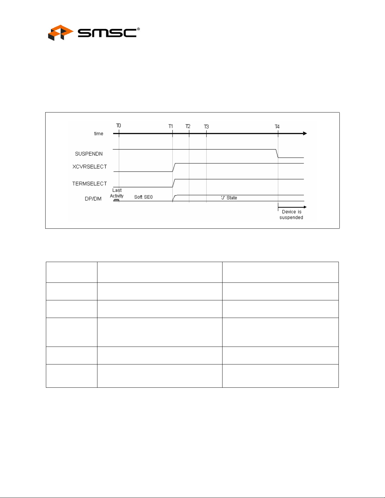
Figure 7.2 Suspend Timing Behavior (HS Mode)
T able 7.6 Suspend Timing Values (HS Mode)
TIMING
PARAMETER DESCRIPTION VALUE
HS Reset T0 End of last bus activity, signaling either a reset
or a SUSPEND.
T1 The time at which the device must place i tself
in FS mode after bus activity stops.
T2 Link samples LINESTATE. If LINESTATE = 'J',
then the initial SE0 on the bus (T0 - T1) had
been due to a Suspend state and the Link
remains in HS mode.
T3 The earliest time where a device can issue
Resume signaling.
T4 The latest time that a device must actually be
suspended, drawing no more than the
suspend current from the bus.
0 (reference)
HS Reset T0 + 3. 0ms < T1 < HS Reset T0
+ 3.125ms
T1 + 100 µs < T2 <
T1 + 875µs
HS Reset T0 + 5ms
HS Reset T0 + 10ms
Revision 1.0 (06-05-08) 34 SMSC USB3500
DATASHEET

Hi-Speed USB Host, Device or OTG PHY With UTMI+ Interface
Datasheet
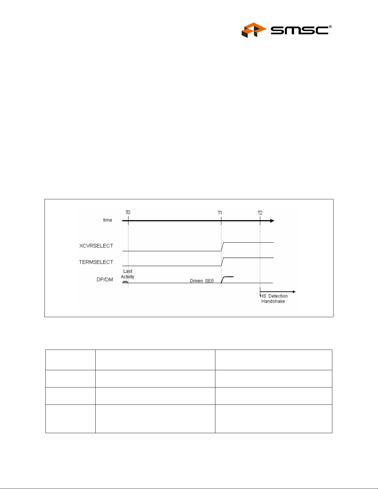
7.7 HS Detection Handshake
The downstream facing port asserting an SE0 state on the bus initiates the HS Detection Hand shake.
There are three ways in which a device may enter the HS Handshake Detection process:
1. If the device is suspended and it detects an SE0 state on the bus it may immediately enter the HS
handshake detection process.
2. If the device is in FS mode and an SE0 state is detected for more than 2.5µs. it may enter the HS
handshake detection process.
3. If the device is in HS mode and an SE0 state is detected for more than 3.0ms. it may enter the
HS handshake detection process. In HS mode, a device must first determine whether the SE0 state
is signaling a suspend or a reset condition. To do this the device reverts to FS mode by placing
XCVRSELECT and TERMSELECT into FS mode. The device must not wait more than 3.125ms
before the reversion to FS mode. After reverting to FS mode, no less than 100µs and no more
than 875µs later the Link must check the LINESTATE signal s. If a J state is detected the device
will enter a suspend state. If an SE0 state is detected, then the device will enter th e HS Handsh ake
detection process.
In each case, the assertion of the SE0 state on the bus initiates the reset. The minimu m reset interval
is 10ms. Depending on the previous mode that the bus was in, the delay between the initial asserti on
of the SE0 state and entering the HS Handshake detection can be from 0 to 4ms.
This transceiver design pushes as much of the responsibility for timing events on to the Link as
possible, and the Link requires a stable CLKOUT signal to perform accurate timing. In case 2 and 3
above, CLKOUT has been running and is stable, however in case 1 the USB3500 is reset from a
suspend state, and the internal oscillator and clocks of the transceiver are assumed to be powered
down. A device has up to 6ms after the release of SUSPENDN to assert a minimum of a 1ms Chirp K.
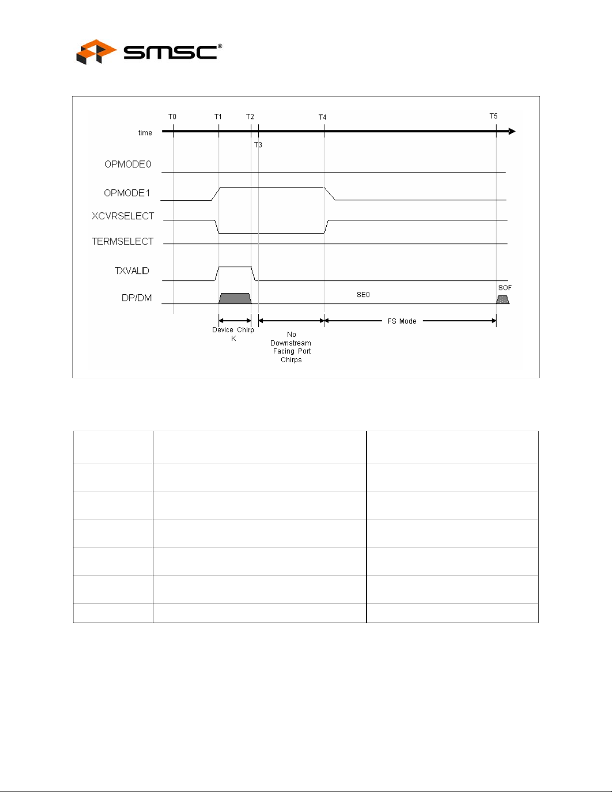
7.8 HS Detection Handshake – FS Downstream Facing Port
Upon entering the HS Detection process (T0), XCVRSELECT and TERMSELECT are in FS mode.
The DP pull-up is asserted and the HS terminations are disabled. The Link then sets OPMODE to
Disable Bit Stuffing and NRZI encoding, XCVRSELECT to HS mode, and begins the transmission of
all 0's data, which asserts a HS K (chirp) on the bus (T1). The device chirp must last at least 1.0ms,
and must end no later than 7.0ms after HS Reset T0. At time T1 the device b egins listening for a chirp
sequence from the host port.
If the downstream facing port is not HS capable, then the HS K asserted by the device is ignored and
the alternating sequence of HS Chirp K’s and J’s is not generated. If no chirps are detected (T4) by
the device, it will enter FS mode by returning XCVRSELECT to FS mode.
SMSC USB3500 35 Revision 1.0 (06-05-08)
DATASHEET
Hi-Speed USB Host, Device or OTG PHY With UTMI+ Interface
Datasheet
Figure 7.3 HS Detection Handshake Timing Behavior (FS Mode)
T able 7.7 HS Detection Handshake Timing Values (FS Mode)
TIMING
PARAMETER DESCRIPTION VALUE
T0 HS Handshake begins. DP pull-up enabled, HS
0 (reference)
terminations disabled.
T1 Device enables HS Transceiver and asserts Chirp
T0 < T1 < HS Reset T0 + 6.0ms
K on the bus.
T2 Device removes Chirp K from the bus. 1ms
minimum width.
T3 Earliest time when d ownstream facing port may
T1 + 1.0 ms < T2 <
HS Reset T0 + 7.0ms
T2 < T3 < T2+100µs
assert Chirp KJ sequence on the bus.
T4 Chirp not detected by the device. Device reverts to
FS default state and waits for end of reset.
T2 + 1.0ms < T4 <
T2 + 2.5ms
T5 Earliest time at which h ost port may end reset HS Reset T0 + 10ms
Notes:
T0 may occur to 4ms after HS Reset T0.
The Link must assert the Chirp K for 66000 CLKOUT cycles to ensure a 1ms min imum duration.
Revision 1.0 (06-05-08) 36 SMSC USB3500
DATASHEET

Hi-Speed USB Host, Device or OTG PHY With UTMI+ Interface
Datasheet
7.9 HS Detection Handshake – HS Downstream Facing Port
Upon entering the HS Detection process (T0), XCVRSELECT and TERMSELECT are in FS mode.
The DP pull-up is asserted and the HS terminations are disabled. The Link then sets OPMODE to
Disable Bit Stuffing and NRZI encoding, XCVRSELECT to HS mode, and begins the transmission of
all 0's data, which asserts a HS K (chirp) on the bus (T1). The device chirp must last at least 1.0ms,
and must end no later than 7.0ms after HS Reset T0. At time T1 the device b egins listening for a chirp
sequence from the downstream facing port. If the downstream facing port is HS capable, then it will
begin generating an alternating sequence of Chirp K’s and Chirp J’s (T3) after the termination of the
chirp from the device (T2). After the device sees the valid chirp sequence Chirp K-J-K-J-K-J (T6), it
will enter HS mode by setting TERMSELECT to HS mode (T7).
Figure 7.4 provides a state diagram for Chirp K-J-K-J-K-J validation. Prior to the end of reset (T9) the
device port must terminate the sequence of Chirp K’s and Chirp J’s (T8) and assert SE0 (T8-T9). Note
that the sequence of Chirp K’s and Chirp J’s constitutes bus activity.
Start Chirp
K-J-K-J-K-J
detection
Chirp Count
= 0
Detect K?
!K
Chirp Count != 6
& !SE0
K State
INC Chirp
Count
Chirp
Invalid
SE0
!J
Detect J?
J State
INC Chirp
Count
Chirp Count
Chirp Valid
Chirp Count != 6
& !SE0
Figure 7.4 Chirp K-J-K-J-K-J Sequence Detection State Diagram
The Chirp K-J-K-J-K-J sequence occurs too slow to propagate through the serial data path, therefore
LINESTATE signal transitions must be used by the Link to step through the Chirp K-J-K-J-K-J state
diagram, where “K State” is equivalent to LINESTATE = K State and “J State” is equivalent to
LINESTATE = J State. The Link must employ a count er (Chirp Count) to count the number of Chirp K
and Chirp J states. Note that LINESTATE does not filter the bus signals so the re quirement that a bus
state must be “continuously asserted for 2.5µs” must be verified by the Link sampling the LINESTATE
signals.
SMSC USB3500 37 Revision 1.0 (06-05-08)
DATASHEET

Hi-Speed USB Host, Device or OTG PHY With UTMI+ Interface
Datasheet
Figure 7.5 HS Detection Handshake Timing Behavior (HS Mode)
T ab le 7.8 Reset Timing Values
TIMING
PARAMETER DESCRIPTION VALUE
T0 HS Handshake begins. DP pull-up enab led, HS
terminations disabled.
T1 Device asserts Chirp K on the bus. T0 < T1 < HS Reset T0 + 6.0ms
T2 Device removes Chirp K from the bus. 1 ms
minimum width.
T3 Downstream facing port asserts Chirp K on the
bus.
T4 Downstream facing port toggles Chirp K to Chirp J
on the bus.
T5 Downstream facing port toggles Chirp J to Chirp K
on the bus.
T6 Device detects downstream port chirp. T6
T7 Chirp detected by the device. Device removes DP
pull-up and asserts HS terminations, reverts to HS
default state and waits for end of reset.
0 (reference)
T0 + 1.0ms < T2 <
HS Reset T0 + 7.0ms
T2 < T3 < T2+100µs
T3 + 40µs < T4 < T3 + 60µs
T4 + 40µs < T5 < T4 + 60µs
T6 < T7 < T6 + 500µs
T8 T erminate host port Chirp K-J sequence (Repeating
T4 and T5)
T9 The earliest time at which host port may end rese t.
The latest time, at which the device may remove
the DP pull-up and assert the HS terminations,
reverts to HS default state.
Revision 1.0 (06-05-08) 38 SMSC USB3500
T9 - 500µs < T8 < T9 - 100µs
HS Reset T0 + 10ms
DATASHEET
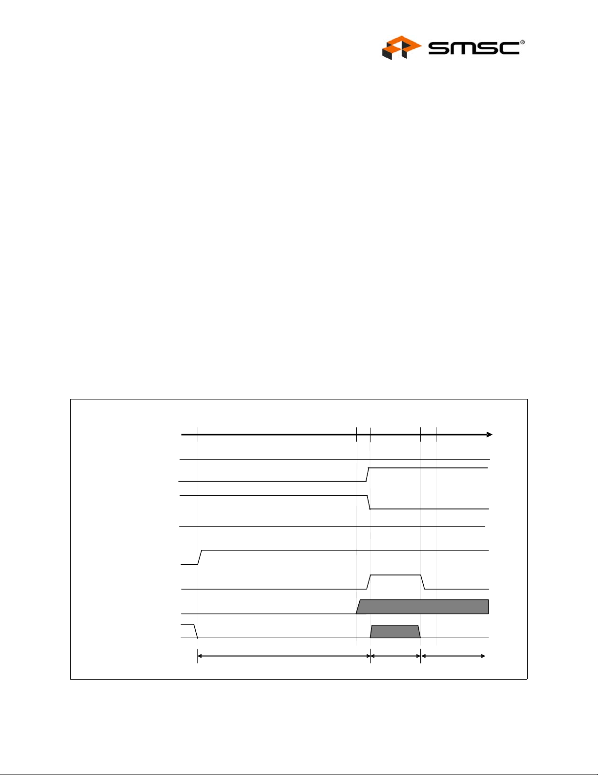
Hi-Speed USB Host, Device or OTG PHY With UTMI+ Interface
Datasheet
Notes:
T0 may be up to 4ms after HS Reset T0.
The Link must use LINESTATE to detect the downstrea m port chirp sequence.
Due to the assertion of the HS termination on t he host port and FS termination on the devi ce port,
between T1 and T7 the signaling levels on the b us are higher than HS signaling levels and are
less than FS signaling levels.
7.10 HS Detection Handshake – Suspend Timing
If reset is entered from a suspended state, the internal oscillator and clocks of the transceiver are
assumed to be powered down. Figure 7.6 shows how CLKOUT is used to control the duration of the
chirp generated by the device.
When reset is entered from a suspended state (J to SE0 transition reported by LINESTATE),
SUSPENDN is combinatorially negated at time T0 by the Link. It takes approximately 5 milliseconds
for the transceiver's oscillator to stabilize. The device does not generate any transitions of the CLKOUT
signal until it is “usable” (where “usable” is defined as stable to within ±10% of the nominal frequency
and the duty cycle accuracy 50±5%).
The first transition of CLKOUT occurs at T1. The Link then sets OPMODE to Disable Bit Stuffing and
NRZI encoding, XCVRSELECT to HS mode, and must assert a Chirp K for 66000 CLKOUT cycles to
ensure a 1ms minimum duration. If CLKOUT is 10% fast (66MHz) then Chirp K will be 1.0ms. If
CLKOUT is 10% slow (54 MHz) then Chirp K will be 1.2ms. The 5.6ms requirement for the first
CLKOUT transition after SUSPENDN, ensures enough time to assert a 1ms Chirp K and still complete
before T3. Once the Chirp K is completed (T3) the Link can begin looking for host chirps and use
CLKOUT to time the process. At this time, the device follows the same protocol as in Section 7.9, "HS
Detection Handshake – HS Downstream Facing Port" for completio n of the High Speed Handshake.
time
OPMODE 0
OPMODE 1
XCVRSELECT
TERMSELECT
SUSPENDN
TXVALID
CLK60
DP/DM
T0
J
SE0
CLK power up time
T1
T2
Device Chirp K
T3 T4
Look for host chirps
Figure 7.6 HS Detection Handshake Timing Behavior from Suspend
SMSC USB3500 39 Revision 1.0 (06-05-08)
DATASHEET
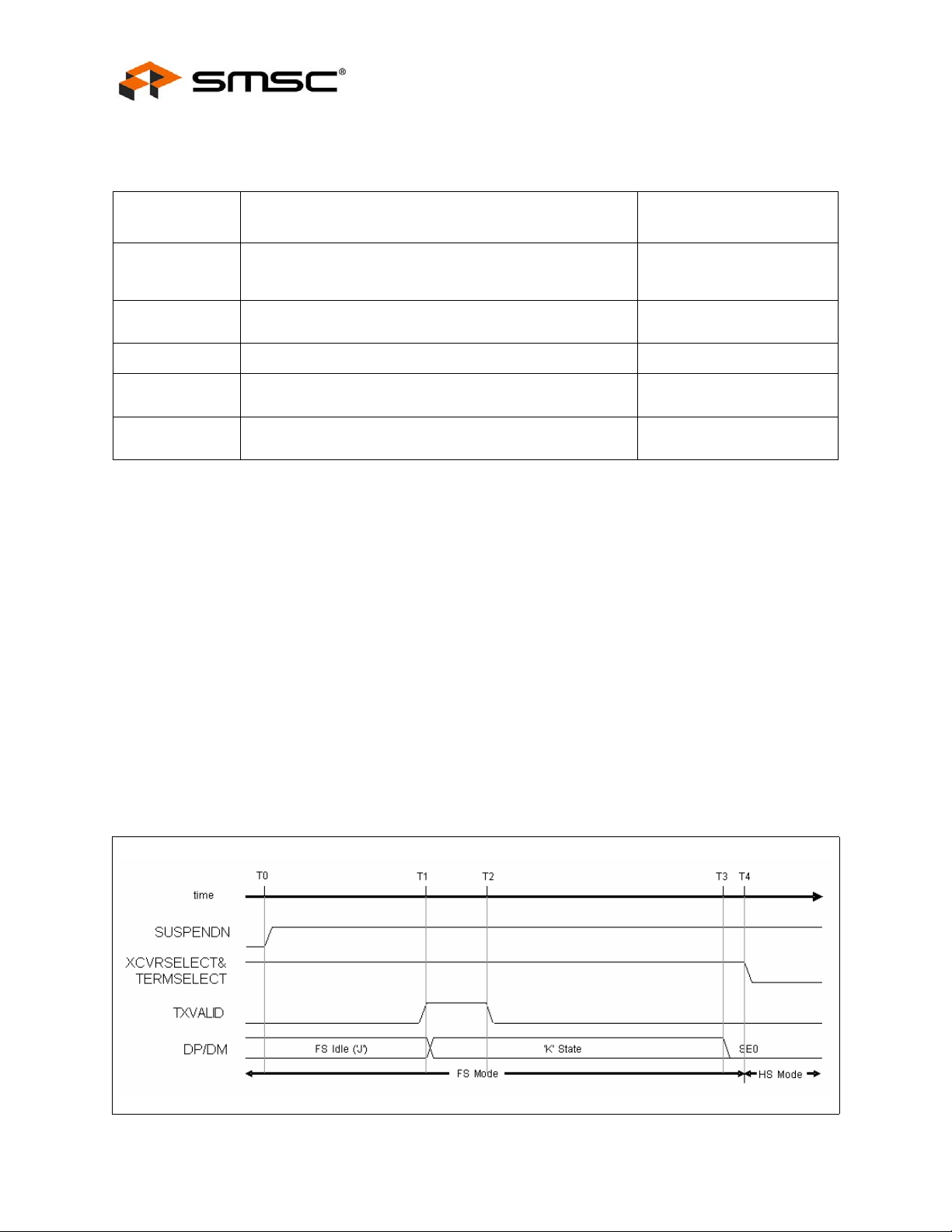
Hi-Speed USB Host, Device or OTG PHY With UTMI+ Interface
Datasheet
To detect the a ssertion of the downstream Chirp K's and Chirp J's for 2.5us {T
the appropriate LINESTATE signals asserted continuously for 165 CLKOUT cycles.
Table 7.9 HS Detection Handshake Timing Values from Suspend
TIMING
PARAMETER DESCRIPTION VALUE
T0 While in suspend state an SE0 is detected on the USB. HS
Handshake begins. D+ pull-up enabled, HS terminations
disabled, SUSPENDN negated.
T1 First transition of CLKOUT. CLKOUT “Usable” (frequency
accurate to ±10%, duty cycle accurate to 50±5).
T2 Device asserts Chirp K on the bus. T 1 < T2 < T0 + 5.8ms
T3 Device removes Chirp K from the bus. (1 ms minimum width)
and begins looking for host chirps.
T4 CLK “Nominal” (CLKOUT is frequency accurate to ±500 ppm,
duty cycle accurate to 50±5).
0 (HS Reset T0)
T0 < T1 < T0 + 5.6ms
T2 + 1.0 ms < T3 <
T0 + 7.0 ms
T1 < T3 < T0 + 20.0ms
}, the Link must see
FILT
7.11 Assertion of Resume
In this case, an event internal to the device initiates the resume process. A device with remote wakeup capability must wait for at least 5ms after the bus is in the idle state before sending the remote
wake-up resume signaling. This allows the hubs to get into their suspend state and prepare for
propagating resume signaling.
The device has 10ms where it can draw a non-suspend current before it must drive resume signaling.
At the beginning of this period the Link may negate SUSPENDN, allowing the transceiver (and its
oscillator) to power up and stabilize.
Figure 7.7 illustrates the behavior of a device returning to HS mode after being suspended. At T4, a
device that was previously in FS mode would maintain TERMSELECT and XCVR SELECT high.
To generate resume signaling (FS 'K') the device is placed in the “Disable Bit Stuffing and NRZI
encoding” Operational Mode (OPMODE [1:0] = 10), TERMSELECT and XCVRSELECT must be in FS
mode, TXVALID asserted, and all 0's data is presented on the DATA bus for at least 1ms (T1 - T2).
Figure 7.7 Resume Timing Behavior (HS Mode)
Revision 1.0 (06-05-08) 40 SMSC USB3500
DATASHEET

Hi-Speed USB Host, Device or OTG PHY With UTMI+ Interface
Datasheet
Table 7.10 Resume Timing Values (HS Mode)
TIMING
PARAMETER DESCRIPTION VALUE
T0 Internal device event initiating the resume
process
T1 Device asserts FS 'K' on the bus to signal
resume request to downstream port
T2 The device releases FS 'K' on the bus. However
by this time the 'K' state is held by downstream
port.
T3 Downstream port asserts SE0. T1 + 20ms
T4 Latest time at which a device, which was
previously in HS mode, must restore HS mode
after bus activity stops.
7.12 Detection of Resume
Resume signaling always takes place in FS mode (TERMSELECT and XCVRSELECT = FS enabled),
so the behavior for a HS device is identical to that of a FS device. The Link uses the LINESTATE
signals to determine when the USB transitions from the 'J' to the 'K' state and finally to the terminati ng
FS EOP (SE0 for 1.25us-1.5µs.).
The resume signaling (FS 'K') will be asserted for at least 20ms. At the beginning of th is period the
Link may negate SUSPENDN, allowing the transceiver (and its oscillator) to power up and stabilize.
0 (reference)
T0 < T1 < T0 + 10ms.
T1 + 1.0ms < T2 < T1 + 15ms
T3 + 1.33µs {2 Low-speed bit times}
The FS EOP condition is relatively short. Links that simply look for an SE0 cond ition to exit suspend
mode do not necessarily give the transceiver’s clock generator enough time to stabilize. It is
recommended that all Link implementations key off the 'J' to 'K' transition for exiting suspend mode
(SUSPENDN = 1). And within 1.25µs after the transition to the SE0 state (low-speed EOP), the Link
must enable normal operation, i.e. enter HS or FS mod e depending on the mode the device was in
when it was suspended.
If the device was in FS mode: then the Link leaves the F S terminations en abled. After the SE0 expires,
the downstream port will assert a J state for one low-speed bit time, and the bus will enter a FS Idle
state (maintained by the FS terminations).
If the device was in HS mode: then the Link must switch to the FS te rminations before the SE0 expires
(< 1.25µs). After the SE0 expires, the bus will then enter a HS IDLE state (maintained by the HS
terminations).
7.13 HS Device Attach
Figure 7.8 demonstrates the timing of the USB3500 control signals during a device attach event. When
a HS device is attached to an upstream port, power is asserted to the device and the device sets
XCVRSELECT and TERMSELECT to FS mode (time T1).
V
is the +5V power available on the USB cable. Device Reset in Figure 7.8 indicates that V
BUS
within normal operational range as defined in the USB 2.0 specificati on. The assertion of Device Reset
(T0) by the upstream port will initialize the device. By monitoring LINESTATE, the Link state machine
knows to set the XCVRSELECT and TERMSELECT signals to FS mode (T1).
The standard FS technique of using a pull-up resistor on DP to signal the attach of a FS device is
employed. The Link must then check the LINESTAT E signals for SE0. If LINESTATE = SE0 is asserted
BUS
is
SMSC USB3500 41 Revision 1.0 (06-05-08)
DATASHEET

Hi-Speed USB Host, Device or OTG PHY With UTMI+ Interface
Datasheet
at time T2 then the upstream port is forcing the reset state to the device (i.e. Driven SE0). The device
will then reset itself before initiating the HS Detection Handshake protocol.
Figure 7.8 Device Attach Behavior
T able 7.11 Attach and Reset Timing Values
TIMING
PARAMETER DESCRIPTION VALUE
T0 Vbus Valid. 0 (reference)
T1 Maximum time from Vbus valid to when the device
T2
(HS Reset T0)
must signal attach.
Debounce interval. The device now enters the HS
Detection Handshake protocol.
T0 + 100ms < T1
T1 + 100ms < T2
Revision 1.0 (06-05-08) 42 SMSC USB3500
DATASHEET
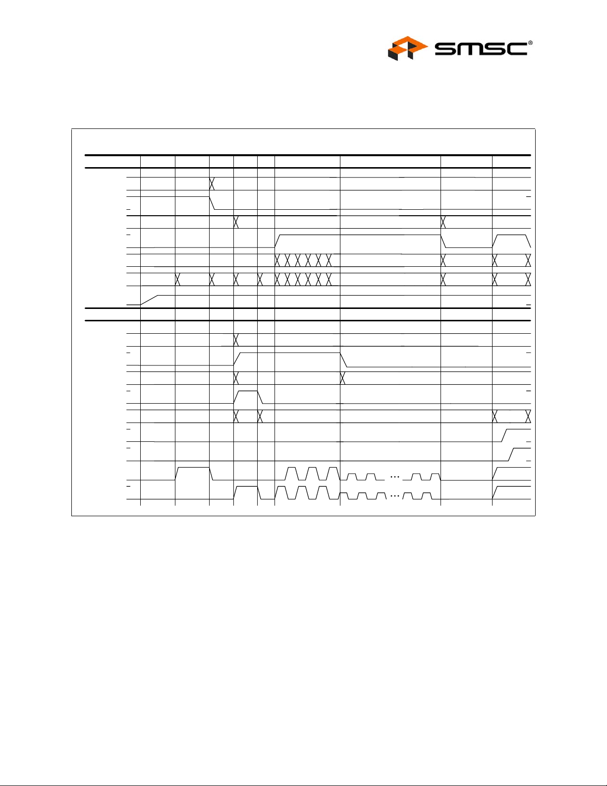
Hi-Speed USB Host, Device or OTG PHY With UTMI+ Interface
Datasheet
7.14 USB Reset and Chirp
The USB 2.0 specification describes USB Reset as a means of attaching a FS or a HS Device to a
Host. This discussion will focus on a HS device connecting to a HS host.
HOST DPPD & DMPD == 1
xcvrselect
termselect
opmode
txvalid
data
linestate
5Volt
vbus
Device DPPD & DMPD == 0
xcvrselect
terms e l e c t
opmode
txvalid
data
rxactive
rxvalid
T1T0 T2
01 00
00
SE0
01
00 10
J
T3 T4
SE0
00h
T5
10
00 FF FF00 00
Kseo
00
KJKJ
T6 T7 T8
00
00-FF
K
K-J
Pairs
00
SE0
00h
HS
SOF
J
A5h
DP
DM
Hs SOF packet
Hs SOF packet
Figure 7.9 USB Reset and Chirp
Figure 7.9 shows the UTMI+ interface for both a Host (DPPD & DMPD = 1) and a Device (DPPD &
DMPD = 0). The following discussion applies to when the USB3500 is a configured as a Device and
is connected to another USB3500 configured as a Host. Since the Host and Device negotiate this
transition, both are discussed together and the user may follow this discussion for either a host or
device depending on the application of the USB35 00. This sequence is also referred to as a “highspeed chirp” due to the K-J pairs which the host sends to the downstream device.
Before the Host begins a session, it will set Xcvrselect to FS mode (10b) and Termselect to 1b to
activate the HS termination. The Host will also asserted the 1 5Kohm pull-down resistors on DP and
DM. The 15Kohm pull down resistors will pull DP and DM to 0 volts so that the Host Linestate will
return Single Ended Zero (SE0) when nothing is attached.
At time marker T0, the host link applies VBUS to th e downstream port.
At T1, the Device has detected a valid voltage on VBUS and has asserted Termselect to enable the
1.5K ohm pull-up resistor on DP. During T1 the Host sees the linestate go from SEO to a J due to the
pull-up on DP.
SMSC USB3500 43 Revision 1.0 (06-05-08)
DATASHEET

Hi-Speed USB Host, Device or OTG PHY With UTMI+ Interface
Datasheet
Note: Note: Should a device attached to the host be a LS device, then the 1.5 K ohm pull-up is
applied to DM. The following discussion does not appl y to a LS device attached.
At T2, the Host has detected the FS device attached to the USB bus. At this time the Host will reset
the bus by driving a SE0. The SE0 is created by switching to HS Mode and activating the HS
termination by de-asserting Termselect. The 45 ohm high speed terminations pull the bus to SE0.
At T3, the Device will respond to the SE0 by driving a “Device Chirp K” onto the bus. Th e “Device
Chirp K” is driven with Opmode = 10b so that bitstuffing and NRZI encoding is disabled.
During T3 the HS host will see the “Device Chirp K” and prepare to respond to the device by setting
Opmode = 10b to disable the bitstuffing and NRZI encoding.
At T4, the Device will stop driving a the Chirp K, letting the bus return to SE0, and wait for the Host
to respond. The device removes the K by de-asserting Txvalid. The device will have driven the K for
a minimum of 1mS. The Host sees the linestate change from K to SE0.
At T5, the host begins transmitting K-J pairs to the device. Each K or J is 40-60uS long and the K-J
pairs are repeated for the remainder of the 10mS USB reset.
At T6, the device has detected 3 K-J pairs. The device switches the Termselect low and changes
Opmode to 00b. The device is now in high speed an d waits for the first SOF packet from the upstream
host. When Termselect is de-asserted , the HS termination is activated which lowers the amplitude of
the K-J pairs.
At T7, the host ends the K-J pairs and switches to normal HS mode by changing Opmode to 00b .
At T8, the Host sends the first SOF packet. This is done by putting the SOF PID 0xA5 on the data
bus and asserting Txvalid. The link transfers the SOF packet. After, the SOF packet a normal high
speed USB session started.
Revision 1.0 (06-05-08) 44 SMSC USB3500
DATASHEET

Hi-Speed USB Host, Device or OTG PHY With UTMI+ Interface
Datasheet
7.15 Application Diagram
3.3 Volt
Supply
4.7uF
VDD3.3
0.1uF
4.7uF
12KΩ
C
0.1uF
LOAD
C
24MHz
LOAD
4.7uF
1MΩ
C
VBUS
Host
Device
OTG Device
5 Volt
Supply
Host Only
USB
Connector
(Standard
or Mini)
Min
100uF
1uF
1uF
VBUS
ID
DP
DM
Max
10uF
6.5uF
C
VBUS
XCVRSEL0
TERMSEL
TXREADY
VBUS
SUSPENDN
TXVALID
RESET
VDD3.3
DP
DM
VDD3.3
RBIAS
VDD3.3
VDD3.3
VDDA1.8XIXO
56555453525150
1
2
3
4
5
ID
6
7
8
9
10
11
12
13
14
15161718192021222324252627
XCVRSEL1
CHRGVBUS
Hi-Speed USB
UTMI+ PHY
56 Pin QFN
RXACTIVE
OPMODE[1]
OPMODE[0]
VDD1.8
49
USB3500
GND FLAG
ID_DIG
IDPULLUP
VBUSVLD
VDD3.3
4847464544
CLKOUT
RXERROR
LINESTATE[0]
LINESTATE[1]
DMPD
DPPD
43
SESSVLD
42
RXVALID
41
40
DATA[0]
39
DATA[1]
38
DATA[2]
37
DATA[3]
36
DATA[4]
35
DATA[5]
34
DATA[6]
33
DATA[7]
32
SESSEND
31
DISCHRGVBUS
30
HOSTDISC
29
28
0.1uF
VDD1.8
VDD3.3
33
UTMI+
Interface
to Link
Figure 7.10 USB3500 Application Diagram (Top View)
SMSC USB3500 45 Revision 1.0 (06-05-08)
DATASHEET

Chapter 8 Package Outline
The USB3500 is offered in a compact 56 lead QFN package.
Hi-Speed USB Host, Device or OTG PHY With UTMI+ Interface
Datasheet
Figure 8.1 USB3500-ABZJ 56 Pin QFN Package Outline, 8 x 8 x 0.9 mm Body (Lead Free)
Table 8.1 56 Terminal QFN Package Parameters
MIN NOMINAL MAX REMARKS
A 0.70 ~ 1.00 Overall Package Height
A1 0 0.02 0.05 Standoff
A2 0.60 ~ 0.90 Mold Thickness
A3 0.20 REF Copper Lead-frame Substrate
D 7.85 8.00 8.15 X Overall Size
D1 7.55 ~ 7.95 X Mold Cap Size
D2 2.25 4.5 6.80 X exposed Pad Si ze
E 7.85 8.00 8.15 Y Overall Size
E1 7.55 ~ 7.95 Y Mold Cap Size
E2 2.25 4.5 6.80 Y ex posed Pad Size
L 0.30 ~ 0.55 Terminal Length
e 0.50 Basic Terminal Pitch
b 0.18 ~ 0.30 Terminal Width
Notes:
1. Controlling Unit: millimeter.
2. Dimension b applies to plated terminals an d is measured between 0.15mm and 0.30mm from the
terminal tip. Tolerance on the true position of the leads is ± 0.05 mm at maximum material
conditions (MMC).
3. Details of terminal #1 identifier are opti onal but must be located within the zone indicated.
Revision 1.0 (06-05-08) 46 SMSC USB3500
DATASHEET
 Loading...