


查询USB3300供应商
USB3300
Hi-Speed USB Host or
Device PHY with ULPI
Low Pin Interface
PRODUCT FEATURES
■ USB-IF “Hi-Speed” certified to the Universal Serial
Bus Specification Rev 2.0
■ Interface compliant with the ULPI Specification
revision 1.1 in 8-bit mode.
■ Industry standard UTMI+ Low Pin Interface (ULPI.)
Converts 54 UTMI+ signals into a standard 12 pin
Link controller interface.
■ Supports FS pre-amble for FS hubs with a LS device
attached (UTMI+ Level 3)
■ Supports HS SOF and LS keep-alive pulse.
■ Includes full support for the optional On-The-Go
(OTG) protocol detailed in the On-The-Go
Supplement Revision 1.0a specification.
■ Supports the OTG Host Negotiation Protocol (HNP)
and Session Request Protocol (SRP.)
■ Allows host to turn VBUS off to conserve battery
power in OTG applications.
■ Supports OTG monitoring of VBUS levels with
internal comparators. Includes support for an external
VBUS or fault monitor.
Data Brief
■ Low Latency Hi-Speed Receiver (43 Hi-Speed clocks
Max) allows use of legacy UTMI Links with a ULPI
wrapper.
■ Integrated Pull-up resistor on STP for interface
protection allows a reliable Link/PHY start-up with
slow Links (software configured for low power.)
■ Internal 1.8 volt regulators allow operation from a
single 3.3 volt supply.
■ Internal short circuit protection of ID, DP and DM
lines to VBUS or ground.
■ Integrated 24MHz Crystal Oscillator supports either
crystal operation or 24MHz external clock input.
■ Internal PLL for 480MHz Hi-Speed USB operation.
■ 54.7mA Unconfigured Current (typical) - ideal for bus
powered applications.
■ 83uA suspend current (typical) - ideal for battery
powered applications.
■ Full Commercial operating temperature range from
0C to +70C.
■ 32 pin QFN package; green, lead-free (5 x 5 x 0.90
mm height)
SMSC USB3300 PRODUCT PREVIEW Revision 1.02 (02-16-05)
e
t
s
r
A
s
R
Hi-Speed USB Host or Device PHY with ULPI Low Pin Interface
ORDER NUMBER(S): USB3300-EZK FOR 32 PIN, QFN PACKAGE (GREEN, LEAD-FREE)
Hauppauge, NY 11788
(631) 435-6000
FAX (631) 273-3123
80 Arkay Drive
Copyright © SMSC 2005. All rights reserved.
Circuit diagrams and other information relating to SMSC products are included as a means of illustrating typical applications. Consequently, complet
information sufficient for construction purposes is not necessarily given. Although the information has been checked and is believed to be accurate, no
responsibility is assumed for inaccuracies. SMSC reserves the right to make changes to specifications and product descriptions at any time withou
notice. Contact your local SMSC sales office to obtain the latest specifications before placing your product order. The provision of this information doe
not convey to the purchaser of the described semiconductor devices any licenses under any patent rights or other intellectual property rights of SMSC
or others. All sales are expressly conditional on your agreement to the terms and conditions of the most recently dated version of SMSC's standard
Terms of Sale Agreement dated before the date of your order (the "Terms of Sale Agreement"). The product may contain design defects or errors
known as anomalies which may cause the product's functions to deviate from published specifications. Anomaly sheets are available upon request.
SMSC products are not designed, intended, authorized or warranted for use in any life support or other application where product failure could cause
or contribute to personal injury or severe property damage. Any and all such uses without prior written approval of an Officer of SMSC and furthe
testing and/or modification will be fully at the risk of the customer. Copies of this document or other SMSC literature, as well as the Terms of Sale
greement, may be obtained by visiting SMSC’s website at http://www.smsc.com. SMSC is a registered trademark of Standard Microsystem
Corporation (“SMSC”). Product names and company names are the trademarks of their respective holders.
SMSC DISCLAIMS AND EXCLUDES ANY AND ALL WARRANTIES, INCLUDING WITHOUT LIMITATION ANY AND ALL IMPLIED WARRANTIES
OF MERCHANTABILITY, FITNESS FOR A PARTICULAR PURPOSE, TITLE, AND AGAINST INFRINGEMENT AND THE LIKE, AND ANY AND
ALL WARRANTIES ARISING FROM ANY COURSE OF DEALING OR USAGE OF TRADE.
IN NO EVENT SHALL SMSC BE LIABLE FOR ANY DIRECT, INCIDENTAL, INDIRECT, SPECIAL, PUNITIVE, OR CONSEQUENTIAL DAMAGES;
OR FOR LOST DATA, PROFITS, SAVINGS OR REVENUES OF ANY KIND; REGARDLESS OF THE FORM OF ACTION, WHETHER BASED ON
CONTRACT; TORT; NEGLIGENCE OF SMSC OR OTHERS; STRICT LIABILITY; BREACH OF WARRANTY; OR OTHERWISE; WHETHER O
NOT ANY REMEDY OF BUYER IS HELD TO HAVE FAILED OF ITS ESSENTIAL PURPOSE, AND WHETHER OR NOT SMSC HAS BEEN
ADVISED OF THE POSSIBILITY OF SUCH DAMAGES.
Revision 1.02 (02-16-05) 2 SMSC USB3300
PRODUCT PREVIEW
Hi-Speed USB Host or Device PHY with ULPI Low Pin Interface
General Description
The USB3300 is a stand-alone Hi-Speed USB Physical Layer Transceiver (PHY). The USB3300 uses
a low pin count interface (ULPI) to connect to a ULPI compliant Link layer. The ULPI interface reduces
the UTMI+ interface from 54 pins to 12 pins using a method of in-band signaling and status byte
transfers between the Link and PHY.
This PHY was designed from the start with the ULPI interface. No UTMI to ULPI wrappers are used
in this design which provides a seamless ULPI to Link interface. The result is a PHY with a low latency
transmit and receive time. SMSC’s low latency high speed and full speed receiver provide the option
of re-using existing UTMI Links with a simple wrapper to convert UTMI to ULPI.
The ULPI interface allows the USB3300 PHY to operate as a device, host, or an On-The-Go (OTG)
device. Designs using the USB3300 PHY as a device, can add host and OTG capability at a later date
with no additional pins.
The ULPI interface, combined with SMSC’s proprietary technology, makes the USB3300 the ideal
method of adding Hi-Speed USB to new designs. The USB3300 features an industry leading small
footprint package (5mm by 5mm) with sub 1mm height. In addition the USB3300 integrates all DP and
DM termination resistances and requires a minimal number of external components.
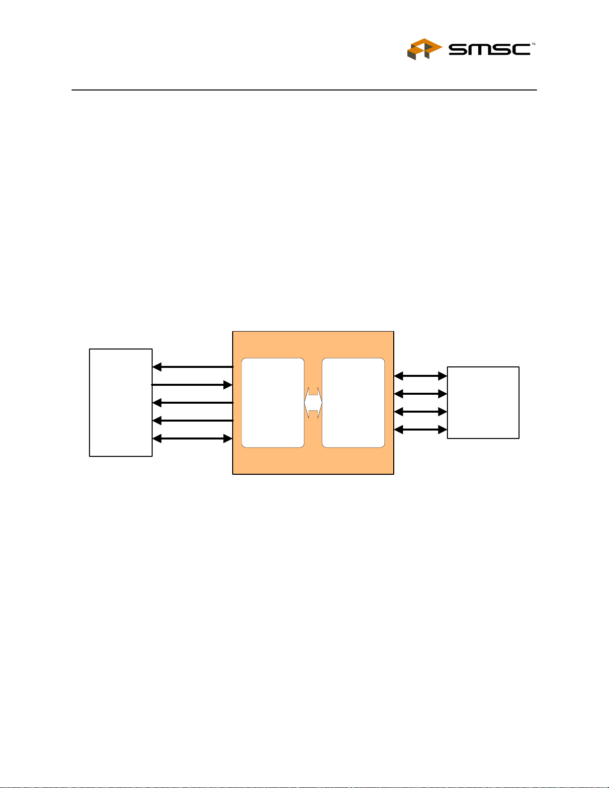
USB3300
ULPI
LINK
CLK
STP
DIR
NXT
DATA[7:0]
ULPI
Digital
Logic
USB 2.0
Analog
w/ OTG
V
ID
DM
DP
BUS
USB
Connector
(Standard
or Mini)
32 Pin QFN
Figure 1 Basic ULPI USB Device Block Diagram
The ULPI interface consists of 12 interface pins; 8 bi-directional data pins, 3 control pins, and a 60
MHz clock. By using the 12 pin ULPI interface the USB3300 is able to provide support for the full range
of UTMI+ Level 3 through Level 0, as shown in Figure 2, "ULPI Interface Features as Related to
UTMI+". This allows USB3300 to work as a HS and FS peripheral and as a HS, FS, and LS Host.
The USB3300 can also, as an option, fully support the On-the-Go (OTG) protocol defined in the OnThe-Go Supplement to the USB 2.0 Specification. On-the-Go allows the USB3300 to function like a
host, or peripheral configured dynamically by software. For example, a cell phone may connect to a
computer as a peripheral to exchange address information or connect to a printer as a host to print
pictures. Finally the OTG enabled device can connect to another OTG enabled device to exchange
information. All this is supported using a single low profile Mini-AB USB connector.
Designs not needing OTG can ignore the OTG feature set.
In addition to the advantages of the leading edge ULPI interface, the use of SMSC’s advanced analog
technology enables the USB3300 to consume a minimum amount of power which results in maximized
battery life for portable applications.
SMSC USB3300 3 Revision 1.02 (02-16-05)
PRODUCT PREVIEW

ADDED FEATURES
Hi-Speed USB Host or Device PHY with ULPI Low Pin Interface
ULPI
USB2.0 Peripheral, host controllers, On-the-
Go devices with 12 pin interface
(HS, FS, LS, preamble packet)
UTMI+ Level 3
USB2.0 Peripheral, host controllers, On-the-
Go devices
(HS, FS, LS, preamble packet)
UTMI+ Level 2
USB2.0 Peripheral, host controllers, On-
the-Go devices
(HS, FS, and LS but no preamble packet)
UTMI+ Level 1
USB2.0 Peripheral, host controllers, and
On-the-Go devices
(HS and FS Only)
USB3300
USB3500
USB3450
Applications
The USB3300 is targeted for any application where a Hi-Speed USB connection is desired and when
board space and interface pins must be minimized.
The USB3300 is well suited for:
■ Cell Phones
■ MP3 Players
■ Scanners
■ External Hard Drives
■ Still and Video Cameras
■ Portable Media Players
■ Entertainment Devices
UTMI+ Level 0
USB2.0 Peripherals Only
Figure 2 ULPI Interface Features as Related to UTMI+
USB3280
USB3250
Revision 1.02 (02-16-05) 4 SMSC USB3300
PRODUCT PREVIEW

Hi-Speed USB Host or Device PHY with ULPI Low Pin Interface
Block Diagram
The USB3300 is a highly integrated USB PHY. It contains a complete Hi-Speed USB2.0 PHY with the
ULPI industry standard interface to support fast time to market for a USB product. The USB3300 is
composed of the functional blocks shown in Figure 3, "USB3300 Block Diagram" below.
VDD3.3
DATA[7:0]
CLKOUT
STP
DIR
NXT
VDD1.8
VDDA1.8
Internal
Regulator &
POR
ULPI Digital
m
24 MHz
XI
XTAL
XTAL &
PLL
HS XCVR
FS/LS
XCVR
USB3300
XO
EXTVBUS
CPEN
OTG
Module
Rpu_dp
Rpu_dm
Rpd_dp
Rpd_dm
Resistors
Bias
Gen.
VBUS
ID
VDD3.3
DP
DM
RBIAS
FAULT
Power
EN
Supply
Mini-AB
USB
Connector
5V
Figure 3 USB3300 Block Diagram
SMSC USB3300 5 Revision 1.02 (02-16-05)
PRODUCT PREVIEW

Hi-Speed USB Host or Device PHY with ULPI Low Pin Interface
Pin Configuration and Pin Definitions
The USB3300 is offered in a 32 pin QFN package (5 x 5 x 0.9mm). The pin definitions and locations
are documented below.
USB3300 Pin Locations
VDD1.8
26
15
VDD1.8
VDD3.3
25
16
VDD3.3
24
23
22
21
20
19
18
17
DATA0
DATA1
DATA2
DATA3
DATA4
DATA5
DATA6
DATA7
GND
GND
CPEN
VBUS
ID
VDD3.3
DP
DM
RBIAS
32
1
2
3
4
5
6
7
8
9
RESET
VDD3.3
VDD3.3
31
Hi-Speed USB2
Hi-Speed USB
10
EXTVBUS
VDDA1.8
30
29
USB3300
USB3300
ULPI PHY
ULPI PHY
32 Pin QFN
32 Pin QFN
GND FLAG
11
12
DIR
NXT
XI
28
13
STP
XO
27
14
CLKOUT
Figure 4 USB3300 Pinout - Top View
The exposed flag of the QFN package must be connected to ground with a via array to the ground
plane. This is the main ground connection for the USB3300.
Pin Definitions, 32-Pin QFN Package
Table 1 USB3300 Pin Definitions
PIN NAME
TYPE
1 GND Ground N/A Ground
2 GND Ground N/A Ground
3 CPEN Output,
CMOS
4 VBUS I/O,
Analog
Revision 1.02 (02-16-05) 6 SMSC USB3300
DIRECTION,
ACTIVE
LEVEL DESCRIPTION
High External 5 volt supply enable. This pin is used to
enable the external Vbus power supply. The CPEN
pin is low on POR.
N/A VBUS pin of the USB cable. The USB3300 uses this
pin for the Vbus comparator inputs and for Vbus
pulsing during session request protocol.
PRODUCT PREVIEW

Hi-Speed USB Host or Device PHY with ULPI Low Pin Interface
Table 1 USB3300 Pin Definitions (continued)
DIRECTION,
PIN NAME
5 ID Input,
6 VDD3.3 Power N/A 3.3V Supply. A 0.1uF bypass capacitor should be
7 DP I/O,
8 DM I/O,
9 RESET Input, CMOS High Optional active high transceiver reset. This is the
10 EXTVBUS Input, CMOS High External Vbus Detect. Connect to fault output of an
11 NXT Output,
TYPE
Analog
Analog
Analog
CMOS
ACTIVE
LEVEL DESCRIPTION
N/A ID pin of the USB cable. For non-OTG applications
this pin can be floated. For an A-Device ID = 0. For
a B-Device ID = 1.
connected between this pin and the ground plane on
the PCB.
N/A D+ pin of the USB cable.
N/A D- pin of the USB cable.
same as a write to the ULPI Reset, address 04h, bit
5. This does not reset the ULPI register set. This
signal must be de-asserted synchronous to
CLKOUT. This pin includes an integrated pull-down
resistor to ground. If not used this pin can be floated
or connected to ground (recommended).
external USB power switch or an external Vbus Valid
comparator.
High The PHY asserts NXT to throttle the data. When the
Link is sending data to the PHY, NXT indicates when
the current byte has been accepted by the PHY. The
Link places the next byte on the data bus in the
following clock cycle.
12 DIR Output,
CMOS
13 STP Input,
CMOS
14 CLKOUT Output,
CMOS
15 VDD1.8 Power N/A 1.8V digital supply. A 0.1uF bypass capacitor to
16 VDD3.3 Power N/A A 0.1uF bypass capacitor should be connected
N/A Controls the direction of the data bus. When the
PHY has data to transfer to the Link, it drives DIR
high to take ownership of the bus. When the PHY
has no data to transfer it drives DIR low and
monitors the bus for commands from the Link. The
PHY will pull DIR high whenever the interface cannot
accept data from the Link, such as during PLL startup.
High The Link asserts STP for one clock cycle to stop the
data stream currently on the bus. If the Link is
sending data to the PHY, STP indicates the last byte
of data was on the bus in the previous cycle.
N/A 60MHz reference clock output. All ULPI signals are
driven synchronous to the rising edge of this clock.
ground is recommended. This pin should be
connected to the other VDD1.8, pin 26.
between this pin and the ground plane on the PCB.
SMSC USB3300 7 Revision 1.02 (02-16-05)
PRODUCT PREVIEW

Hi-Speed USB Host or Device PHY with ULPI Low Pin Interface
Table 1 USB3300 Pin Definitions (continued)
DIRECTION,
PIN NAME
17 DATA[7] I/O,
18 DATA[6] I/O,
19 DATA[5] I/O,
20 DATA[4] I/O,
21 DATA[3] I/O,
22 DATA[2] I/O,
23 DATA[1] I/O,
TYPE
CMOS,
Pull-low
CMOS,
Pull-low
CMOS,
Pull-low
CMOS,
Pull-low
CMOS,
Pull-low
CMOS,
Pull-low
CMOS,
Pull-low
ACTIVE
LEVEL DESCRIPTION
N/A 8-bit bi-directional data bus. Bus ownership is
N/A
N/A
N/A
N/A
N/A
N/A
determined by DIR. The Link and PHY initiate data
transfers by driving a non-zero pattern onto the data
bus. ULPI defines interface timing for a single-edge
data transfers with respect to rising edge of
CLKOUT. DATA[7] is the MSB and DATA[0] is the
LSB.
24 DATA[0] I/O,
CMOS,
Pull-low
25 VDD3.3 Power N/A A 0.1uF bypass capacitor should be connected
26 VDD1.8 Power N/A 1.8V Digital regulator bypass. A 4.7uF low ESR
27 XO Output,
Analog
28 XI Input,
Analog
29 VDDA1.8 Power N/A 1.8 Volt Analog Regulator bypass. A 4.7uF low ESR
30 VDD3.3 Power N/A Analog 3.3 volt supply. A 0.1uF low ESR bypass
31 VDD3.3 Power N/A Analog 3.3 volt supply. Should be connected directly
N/A
between this pin and the ground plane on the PCB.
ceramic bypass capacitor should be connected
between this pin and the ground plane of the PCB.
This pin should be connected to the other VDD1.8,
pin 15.
N/A Crystal pin. If using an external clock on XI this pin
should be floated.
N/A Crystal pin. A 24MHz crystal is supported. The
crystal is placed across XI and XO. An external
24MHz clock source may be driven into XI in place
of a crystal.
ceramic bypass capacitor to the ground plane of the
PCB is recommended.
capacitor connected to the ground plane of the PCB
is recommended.
to pin 30.
32 RBIAS Analog,
CMOS
Revision 1.02 (02-16-05) 8 SMSC USB3300
N/A External 12KΩ +/- 1% bias resistor to ground.
PRODUCT PREVIEW

Hi-Speed USB Host or Device PHY with ULPI Low Pin Interface
Table 1 USB3300 Pin Definitions (continued)
DIRECTION,
PIN NAME
GND FLAG Ground N/A Ground. The flag must be connected to the ground
Application Notes
Application Diagram
Max
10uF
6.5uF
4.7uF
VDD3.3
0.1uF
3.3 Volt
Supply
C
VBUS
Host
Device
OTG Device
USB
Connector
(Standard
or Mini)
Min
100uF
1uF
1uF
TYPE
CPEN
VBUS
VDD3.3
DP
DM
ACTIVE
LEVEL DESCRIPTION
plane with a via array under the exposed flag. This
is the main ground for the IC.
C
28
13
XO
27
14
LOAD
VDD1.8
26
15
1MΩ
24MHz
C
LOAD
4.7uF
VDD3.3
25
16
24
23
22
21
20
19
18
17
DATA0
DATA1
DATA2
DATA3
DATA4
DATA5
DATA6
DATA7
(MSB)
0.1uF
4.7uF
1
2
3
4
ID
5
6
7
8
0.1uF
12KΩ
RBIAS
VDD3.3
VDD3.3
32
31
30
USB3300
USB3300
Hi-Speed USB2
Hi-Speed USB2
ULPI PHY
ULPI PHY
32 Pin QFN
32 Pin QFN
GND FLAG
9
10
11
VDDA1.8
XI
29
12
C
VBUS
5 Volt
Supply
Host Only
Fault
RESET
EXTVBUS
NXT
DIR
STP
VDD3.3
VDD1.8
CLKOUT
12
ULPI Interface
to LINK
Figure 5 USB3300 Application Diagram
In addition to the 4.7uF VDD3.3 bypass capacitor, it is recommend that each power pin have a
capacitor to ground alternating between 0.1uF and 0.01uF (not shown for clarity).
SMSC USB3300 9 Revision 1.02 (02-16-05)
PRODUCT PREVIEW

Multi-Port Applications
To support multiple ports a single USB3300 host can be combined with one of SMSC’s many hub
products to expand the number of ports. SMSC has 2-port, 3-port, 4-port, and 7-port hub designs which
can be used to expand the number of ports in a design.
Hi-Speed USB Host or Device PHY with ULPI Low Pin Interface
DIR
NXT
STP
CLOCK
DATA[7]
DATA[6]
DATA[5]
DATA[4]
DATA[3]
DATA[2]
DATA[1]
DATA[0]
SOC w/
ULPI Link
Using a SMSC hub to expand the number of ports allows a single Link to run several USB devices
without a separate Link to support each USB port. Another advantage of using a SMSC hub is on
products where the main board is not located near the USB ports. The USB3300 can be placed on
the main board with the Link ASIC and the hub can be placed on a separate board next to the USB
ports. The only data connection required between the boards is DP and DM.
DIR
NXT
STP
CLOCK
DATA[7]
DATA[6]
DATA[5]
DATA[4]
DATA[3]
DATA[2]
DATA[1]
DATA[0]
CPEN
DP
DM
VBUS_DET
USBDP0
USBDM0
USB2502
USBDP1
USBDN1
USBDP2
USBDN2
USBDP3
USBDN3
USB2503
USB3300
USBDP4
USBDN4
USB2504
USBDP5-7
USBDN5-7
USB2507
Figure 6 Expanding Downstream Ports for USB3300 Host Applications
USB Port 1
DP
DM
USB Port 2
DP
DM
USB Port 3
DP
DM
USB Port 4
DP
DM
USB Ports 5-7
DP
DM
The CPEN output of the USB3300 is optional and can be used to turn the Hub on or off to lower current
when the USB connection isn’t needed.
Evaluation Board
An evaluation board, EVB-USB3300, is available for building a prototype system with the USB3300.
The evaluation board provides an industry standard T&MT connector to interface a ULPI Link controller
and a Mini-AB connector for the USB cable. A 500mA fault protected 5V Vbus switch that is controlled
by the USB3300 is also included.
Supporting Documentation
■ Universal Serial Bus Specification, Revision 2.0, April 27, 2000
■ On-The-Go Supplement to the USB 2.0 Specification, Revision 1.0a, June 24, 2003
■ USB 2.0 Transceiver Macrocell Interface (UTMI) Specification, Version 1.02, May 27, 2000
■ UTMI+ Specification, Revision 1.0, February 2, 2004
■ UTMI+ Low Pin Interface (ULPI) Specification, Revision 1.1
Revision 1.02 (02-16-05) 10 SMSC USB3300
PRODUCT PREVIEW

Hi-Speed USB Host or Device PHY with ULPI Low Pin Interface
Package Outline
The USB3300 is offered in a compact 32 lead-free QFN package.
Figure 7 USB3300-EZK 32 Pin QFN Package Outline, 5 x 5 x 0.9 mm Body (Lead-Free)
Table 2 32 Terminal QFN Package Parameters
MIN NOMINAL MAX REMARKS
A 0.80 ~ 1.00 Overall Package Height
A1 0 ~ 0.05 Standoff
A2 0.60 ~ 0.80 Mold Thickness
A3 0.20 REF Copper Lead-frame Substrate
D 4.85 ~ 5.15 X Overall Size
D1 4.55 ~ 4.95 X Mold Cap Size
D2 1.25 3.5 3.80 X exposed Pad Size
E 4.85 ~ 5.15 Y Overall Size
E1 4.55 ~ 4.95 Y Mold Cap Size
E2 1.25 3.5 3.80 Y exposed Pad Size
L 0.30 ~ 0.50 Terminal Length
e 0.50 Basic Terminal Pitch
b 0.18 ~ 0.30 Terminal Width
ccc ~ ~ 0.08 Coplanarity
Notes:
1. Controlling Unit: millimeter.
2. Dimension b applies to plated terminals and is measured between 0.15mm and 0.30mm from the
terminal tip. Tolerance on the true position of the leads is ± 0.05 mm at maximum material
conditions (MMC).
3. Details of terminal #1 identifier are optional but must be located within the zone indicated.
4. Coplanarity zone applies to exposed pad and terminals.
SMSC USB3300 11 Revision 1.02 (02-16-05)
PRODUCT PREVIEW
 Loading...