

Page 1

USB3280
Hi-Speed USB Device
PHY with UTMI Interface
PRODUCT FEATURES
Available in a 36-pin lead-free RoHS compliant (6 x 6
x 0.90mm) QFN package
Interface compl iant with the UTMI specification
(60MHz, 8-bit bidirectional interface)
Only o ne required power supply (+3.3V)
USB-IF “Hi -Speed” certified to USB 2.0 electrical
specification
Sup ports 480Mbps Hi-Speed (HS) and 12Mbps Full
Speed (FS) serial data transmission rates
Integra ted 45Ω and 1.5kΩ termination resistors
reduce external component count
Internal short circuit protection of DP and DM lines
On-chip oscillator operates with low cost 24MHz
crystal
Latch-up performance exceeds 150mA per EIA/JESD
78, Class II
ESD p rotection levels of 5kV HBM without external
protection devices
SYNC an d EOP generation on transmit packets and
detection on receive packets
NR ZI encoding and decoding
Bit stuffing and unstuffing with error detection
Sup ports the USB suspend state, HS detection, HS
Chirp, Reset and Resume
Sup port for all test modes defined in the USB 2.0
specification
5 5mA Unconfigured Current (typical) - ideal for bus
powered applications.
8 3uA suspend current (typical) - ideal for battery
powered applications.
Indu strial Operating Temperature -40
o
C to +85oC
Datasheet
Applications
The USB3280 is the ideal companion to any ASIC, SoC
or FPGA solution designed with a UTMI Hi-Speed USB
device (peripheral) core.
The USB3280 is well suited for:
C ell Phones
MP3 Pl ayers
Scanners
Externa l Hard Drives
D igital Still and Video Cameras
Po rtable Media Players
En tertainment Devices
Printers
SMSC USB3280 DATASHEET Revision 1.5 (11-15-07)
Page 2

Hi-Speed USB Device PHY with UTMI Interface
ORDER NUMBER(S):
USB3280-AEZG FOR 36-PIN, QFN LEAD-FREE ROHS COMPLIANT PACKAGE
USB3280-AEZG-TR FOR 36-PIN, QFN LEAD-FREE ROHS COMPLIANT PACKAGE (TAPE AND REEL)
Reel Size is 3000 pieces.
Datasheet
80 ARKAY DRIVE, HAUPPAUGE, NY 11788 (631) 435-6000, FAX (631) 273-3123
Copyright © 2007 SMSC or its subsidiaries. All rights reserved.
Circuit diagrams and other information relating to SMSC products are included as a mean s of illustrating typical applications. Conse quently, complete information sufficient for
construction purposes is not necessarily given. Although the information has been checked and is believed to be accurate, no responsibility is assumed for inaccuracies. SMSC
reserves the right to make changes to specifications and product descriptions at any time without notice. Contact your local SMSC sales office to obtain the latest specifications
before placing your product order. The provision of this information does not convey to the purchaser of the described semiconductor devices any licenses under any patent
rights or other intellectual property rights of SMSC or others. All sales are expressly conditional on your agreement to the terms and conditions of the most recently da ted
version of SMSC's standard Terms of Sale Agreement dated before the date of your order (the "Terms of Sale Agreement"). The product may contain design defects or errors
known as anomalies which may cause the product's functions to deviate from published specifications. Anomaly sheets are available upon request. SMSC products are not
designed, intended, authorized or warranted for use in any life support or other application where product failure could cause or contribute to personal injury or severe property
damage. Any and all such uses without prior written approval of an Officer of SMSC and further testing and/or modification will be fully at the risk of the customer. Copies of
this document or other SMSC literature, as well as the Terms of Sale Agreement, may be obtained by visiting SMSC’s website at http://www.smsc.com. SMSC is a registered
trademark of Standard Microsystems Corporation (“SMSC”). Product names and company names are the trademarks of their respective holders.
SMSC DISCLAIMS AND EXCLUDES ANY AND ALL WARRANTIES, INCLUDING WITHOUT LIMITATION ANY AND ALL IMPLIED WARRANTIES OF MERCHANTABILITY,
FITNESS FOR A PARTICULAR PURPOSE, TITLE, AND AGAINST INFRINGEMENT AND THE LIKE, AND ANY AND ALL WARRANTIES ARISING FROM ANY COURSE
OF DEALING OR USAGE OF TRADE. IN NO EVENT SHALL SMSC BE LIABLE FOR ANY DIRECT, INCIDENTAL, INDIRECT, SPECIAL, PUNITIVE, OR CONSEQUENTIAL
DAMAGES; OR FOR LOST DATA, PROFITS, SAVINGS OR REVENUES OF ANY KIND; REGARDLESS OF THE FORM OF ACTION, WHETHER BASED ON CONTRACT;
TORT; NEGLIGENCE OF SMSC OR OTHERS; STRICT LIABILITY; BREACH OF WARRANTY; OR OTHERWISE; WHETHER OR NOT ANY REMEDY OF BUYER IS HELD
TO HAVE FAILED OF ITS ESSENTIAL PURPOSE, AND WHETHER OR NOT SMSC HAS BEEN ADVISED OF THE POSSIBILITY OF SUCH DAMAGES.
Revision 1.5 (11-15-07) 2 SMSC USB3280
DATASHEET
Page 3

Hi-Speed USB Device PHY with UTMI Interface
Datasheet
Table of Contents
Chapter 1 General Description. . . . . . . . . . . . . . . . . . . . . . . . . . . . . . . . . . . . . . . . . . . . . . . . . 6
1.1 Product Description . . . . . . . . . . . . . . . . . . . . . . . . . . . . . . . . . . . . . . . . . . . . . . . . . . . . . . . . . . . . . 6
Chapter 2 Functional Block Diagram . . . . . . . . . . . . . . . . . . . . . . . . . . . . . . . . . . . . . . . . . . . 7
Chapter 3 Pinout . . . . . . . . . . . . . . . . . . . . . . . . . . . . . . . . . . . . . . . . . . . . . . . . . . . . . . . . . . . . 8
Chapter 4 Interface Signal Definition . . . . . . . . . . . . . . . . . . . . . . . . . . . . . . . . . . . . . . . . . . . 9
Chapter 5 Limiting Values . . . . . . . . . . . . . . . . . . . . . . . . . . . . . . . . . . . . . . . . . . . . . . . . . . . 12
Chapter 6 Electrical Characteristics . . . . . . . . . . . . . . . . . . . . . . . . . . . . . . . . . . . . . . . . . . . 13
6.1 Driver Characteristics of Full-Speed Drivers in High-Speed Capable Transceivers. . . . . . . . . . . . 16
6.2 High-speed Signaling Eye Patterns . . . . . . . . . . . . . . . . . . . . . . . . . . . . . . . . . . . . . . . . . . . . . . . . 18
Chapter 7 Functional Overview . . . . . . . . . . . . . . . . . . . . . . . . . . . . . . . . . . . . . . . . . . . . . . . 21
7.1 Modes of Operation . . . . . . . . . . . . . . . . . . . . . . . . . . . . . . . . . . . . . . . . . . . . . . . . . . . . . . . . . . . . 21
7.2 System Clocking. . . . . . . . . . . . . . . . . . . . . . . . . . . . . . . . . . . . . . . . . . . . . . . . . . . . . . . . . . . . . . . 21
7.3 Clock and Data Recovery Circuit . . . . . . . . . . . . . . . . . . . . . . . . . . . . . . . . . . . . . . . . . . . . . . . . . . 22
7.4 TX Logic . . . . . . . . . . . . . . . . . . . . . . . . . . . . . . . . . . . . . . . . . . . . . . . . . . . . . . . . . . . . . . . . . . . . . 22
7.5 RX Logic. . . . . . . . . . . . . . . . . . . . . . . . . . . . . . . . . . . . . . . . . . . . . . . . . . . . . . . . . . . . . . . . . . . . . 23
7.6 USB 2.0 Transceiver. . . . . . . . . . . . . . . . . . . . . . . . . . . . . . . . . . . . . . . . . . . . . . . . . . . . . . . . . . . . 26
7.6.1 High Speed and Full Speed Transceivers. . . . . . . . . . . . . . . . . . . . . . . . . . . . . . . . . . . . 26
7.6.2 Termination Resistors . . . . . . . . . . . . . . . . . . . . . . . . . . . . . . . . . . . . . . . . . . . . . . . . . . . 26
7.6.3 Bias Generator . . . . . . . . . . . . . . . . . . . . . . . . . . . . . . . . . . . . . . . . . . . . . . . . . . . . . . . . 27
7.7 Crystal Oscillator and PLL . . . . . . . . . . . . . . . . . . . . . . . . . . . . . . . . . . . . . . . . . . . . . . . . . . . . . . . 27
7.8 Internal Regulators and POR . . . . . . . . . . . . . . . . . . . . . . . . . . . . . . . . . . . . . . . . . . . . . . . . . . . . . 27
7.8.1 Internal Regulators . . . . . . . . . . . . . . . . . . . . . . . . . . . . . . . . . . . . . . . . . . . . . . . . . . . . . 27
7.8.2 Power On Reset (POR). . . . . . . . . . . . . . . . . . . . . . . . . . . . . . . . . . . . . . . . . . . . . . . . . . 27
7.8.3 Reset Pin. . . . . . . . . . . . . . . . . . . . . . . . . . . . . . . . . . . . . . . . . . . . . . . . . . . . . . . . . . . . . 27
Chapter 8 Application Notes. . . . . . . . . . . . . . . . . . . . . . . . . . . . . . . . . . . . . . . . . . . . . . . . . . 28
8.1 Linestate. . . . . . . . . . . . . . . . . . . . . . . . . . . . . . . . . . . . . . . . . . . . . . . . . . . . . . . . . . . . . . . . . . . . . 28
8.2 OPMODES . . . . . . . . . . . . . . . . . . . . . . . . . . . . . . . . . . . . . . . . . . . . . . . . . . . . . . . . . . . . . . . . . . . 29
8.3 Test Mode Support. . . . . . . . . . . . . . . . . . . . . . . . . . . . . . . . . . . . . . . . . . . . . . . . . . . . . . . . . . . . . 29
8.4 SE0 Handling . . . . . . . . . . . . . . . . . . . . . . . . . . . . . . . . . . . . . . . . . . . . . . . . . . . . . . . . . . . . . . . . . 30
8.5 Reset Detection . . . . . . . . . . . . . . . . . . . . . . . . . . . . . . . . . . . . . . . . . . . . . . . . . . . . . . . . . . . . . . . 30
8.6 Suspend Detection . . . . . . . . . . . . . . . . . . . . . . . . . . . . . . . . . . . . . . . . . . . . . . . . . . . . . . . . . . . . . 31
8.7 HS Detection Handshake . . . . . . . . . . . . . . . . . . . . . . . . . . . . . . . . . . . . . . . . . . . . . . . . . . . . . . . . 32
8.8 HS Detection Handshake – FS Downstream Facing Port . . . . . . . . . . . . . . . . . . . . . . . . . . . . . . . 32
8.9 HS Detection Handshake – HS Downstream Facing Port . . . . . . . . . . . . . . . . . . . . . . . . . . . . . . . 34
8.10 HS Detection Handshake – Suspend Timing . . . . . . . . . . . . . . . . . . . . . . . . . . . . . . . . . . . . . . . . . 36
8.11 Assertion of Resume . . . . . . . . . . . . . . . . . . . . . . . . . . . . . . . . . . . . . . . . . . . . . . . . . . . . . . . . . . . 38
8.12 Detection of Resume . . . . . . . . . . . . . . . . . . . . . . . . . . . . . . . . . . . . . . . . . . . . . . . . . . . . . . . . . . . 39
8.13 HS Device Attach . . . . . . . . . . . . . . . . . . . . . . . . . . . . . . . . . . . . . . . . . . . . . . . . . . . . . . . . . . . . . . 39
8.14 Application Diagram . . . . . . . . . . . . . . . . . . . . . . . . . . . . . . . . . . . . . . . . . . . . . . . . . . . . . . . . . . . . 41
Chapter 9 Package Outline . . . . . . . . . . . . . . . . . . . . . . . . . . . . . . . . . . . . . . . . . . . . . . . . . . . 42
SMSC USB3280 3 Revision 1.5 (11-15-07)
DATASHEET
Page 4

Hi-Speed USB Device PHY with UTMI Interface
Datasheet
List of Figures
Figure 2.1 USB3280 Block Diagram . . . . . . . . . . . . . . . . . . . . . . . . . . . . . . . . . . . . . . . . . . . . . . . . . . . . . 7
Figure 3.1 USB3280 Pinout - Top View . . . . . . . . . . . . . . . . . . . . . . . . . . . . . . . . . . . . . . . . . . . . . . . . . . 8
Figure 3.2 USB3280 Pinout - Bottom View. . . . . . . . . . . . . . . . . . . . . . . . . . . . . . . . . . . . . . . . . . . . . . . . 8
Figure 6.1 Full-Speed Driver VOH/IOH Characteristics for High-speed Capable Transceiver . . . . . . . . 17
Figure 6.2 Full-Speed Driver VOL/IOL Characteristics for High-speed Capable Transceiver. . . . . . . . . 17
Figure 6.3 Eye Pattern Measurement Planes . . . . . . . . . . . . . . . . . . . . . . . . . . . . . . . . . . . . . . . . . . . . . 18
Figure 6.4 Eye Pattern for Transmit Waveform and Eye Pattern Definition . . . . . . . . . . . . . . . . . . . . . . 19
Figure 6.5 Eye Pattern for Receive Waveform and Eye Pattern Definition. . . . . . . . . . . . . . . . . . . . . . . 20
Figure 7.1 FS CLK Relationship to Transmit Data and Control Signals . . . . . . . . . . . . . . . . . . . . . . . . . 21
Figure 7.2 FS CLK Relationship to Receive Data and Control Signals. . . . . . . . . . . . . . . . . . . . . . . . . . 22
Figure 7.3 Transmit Timing for a Data Packet. . . . . . . . . . . . . . . . . . . . . . . . . . . . . . . . . . . . . . . . . . . . . 22
Figure 7.4 Receive Timing for Data with Unstuffed Bits . . . . . . . . . . . . . . . . . . . . . . . . . . . . . . . . . . . . . 23
Figure 7.5 Receive Timing for a Handshake Packet (no CRC). . . . . . . . . . . . . . . . . . . . . . . . . . . . . . . . 24
Figure 7.6 Receive Timing for Setup Packet. . . . . . . . . . . . . . . . . . . . . . . . . . . . . . . . . . . . . . . . . . . . . . 25
Figure 7.7 Receive Timing for Data Packet (with CRC-16). . . . . . . . . . . . . . . . . . . . . . . . . . . . . . . . . . . 25
Figure 8.1 Reset Timing Behavior (HS Mode) . . . . . . . . . . . . . . . . . . . . . . . . . . . . . . . . . . . . . . . . . . . . 30
Figure 8.2 Suspend Timing Behavior (HS Mode) . . . . . . . . . . . . . . . . . . . . . . . . . . . . . . . . . . . . . . . . . . 31
Figure 8.3 HS Detection Handshake Timing Behavior (FS Mode) . . . . . . . . . . . . . . . . . . . . . . . . . . . . . 33
Figure 8.4 Chirp K-J-K-J-K-J Sequence Detection State Diagram . . . . . . . . . . . . . . . . . . . . . . . . . . . . . 34
Figure 8.5 HS Detection Handshake Timing Behavior (HS Mode) . . . . . . . . . . . . . . . . . . . . . . . . . . . . . 35
Figure 8.6 HS Detection Handshake Timing Behavior from Suspend . . . . . . . . . . . . . . . . . . . . . . . . . . 37
Figure 8.7 Resume Timing Behavior (HS Mode) . . . . . . . . . . . . . . . . . . . . . . . . . . . . . . . . . . . . . . . . . . 38
Figure 8.8 Device Attach Behavior . . . . . . . . . . . . . . . . . . . . . . . . . . . . . . . . . . . . . . . . . . . . . . . . . . . . . 40
Figure 8.9 USB3280 Application Diagram. . . . . . . . . . . . . . . . . . . . . . . . . . . . . . . . . . . . . . . . . . . . . . . . 41
Figure 9.1 USB3280-AEZG 36-Pin QFN Package Outline and Parameters, 6 x 6 x 0.90 mm Body (Lead-
Free RoHS Compliant) 42
Figure 9.2 QFN, 6x6 Tape & Reel. . . . . . . . . . . . . . . . . . . . . . . . . . . . . . . . . . . . . . . . . . . . . . . . . . . . . . 43
Figure 9.3 Reel Dimensions . . . . . . . . . . . . . . . . . . . . . . . . . . . . . . . . . . . . . . . . . . . . . . . . . . . . . . . . . . 44
Revision 1.5 (11-15-07) 4 SMSC USB3280
DATASHEET
Page 5

Hi-Speed USB Device PHY with UTMI Interface
Datasheet
List of Tables
Table 4.1 System Interface Signals. . . . . . . . . . . . . . . . . . . . . . . . . . . . . . . . . . . . . . . . . . . . . . . . . . . . . . 9
Table 4.2 Data Interface Signals . . . . . . . . . . . . . . . . . . . . . . . . . . . . . . . . . . . . . . . . . . . . . . . . . . . . . . . 10
Table 4.3 USB I/O Signals. . . . . . . . . . . . . . . . . . . . . . . . . . . . . . . . . . . . . . . . . . . . . . . . . . . . . . . . . . . . 10
Table 4.4 Biasing and Clock Oscillator Signals. . . . . . . . . . . . . . . . . . . . . . . . . . . . . . . . . . . . . . . . . . . . 10
Table 4.5 Power and Ground Signals . . . . . . . . . . . . . . . . . . . . . . . . . . . . . . . . . . . . . . . . . . . . . . . . . . . 11
Table 5.1 Absolute Maximum Ratings. . . . . . . . . . . . . . . . . . . . . . . . . . . . . . . . . . . . . . . . . . . . . . . . . . . 12
Table 5.2 Recommended Operating Conditions . . . . . . . . . . . . . . . . . . . . . . . . . . . . . . . . . . . . . . . . . . . 12
Table 5.3 Recommended External Clock Conditions . . . . . . . . . . . . . . . . . . . . . . . . . . . . . . . . . . . . . . . 12
Table 6.1 Electrical Characteristics: Supply Pins (Note 6.1) . . . . . . . . . . . . . . . . . . . . . . . . . . . . . . . . . . 13
Table 6.2 DC Electrical Characteristics: Logic Pins (Note 6.2) . . . . . . . . . . . . . . . . . . . . . . . . . . . . . . . . 13
Table 6.3 DC Electrical Characteristics: Analog I/O Pins (DP/DM) (Note 6.3) . . . . . . . . . . . . . . . . . . . . 14
Table 6.4 Dynamic Characteristics: Analog I/O Pins (DP/DM) (Note 6.4). . . . . . . . . . . . . . . . . . . . . . . . 15
Table 6.5 Dynamic Characteristics: Digital UTMI Pins (Note 6.5). . . . . . . . . . . . . . . . . . . . . . . . . . . . . . 16
Table 7.1 DP/DM Termination vs. Signaling Mode . . . . . . . . . . . . . . . . . . . . . . . . . . . . . . . . . . . . . . . . . 26
Table 8.1 Linestate States. . . . . . . . . . . . . . . . . . . . . . . . . . . . . . . . . . . . . . . . . . . . . . . . . . . . . . . . . . . . 28
Table 8.2 Operational Modes . . . . . . . . . . . . . . . . . . . . . . . . . . . . . . . . . . . . . . . . . . . . . . . . . . . . . . . . . 29
Table 8.3 USB 2.0 Test Modes . . . . . . . . . . . . . . . . . . . . . . . . . . . . . . . . . . . . . . . . . . . . . . . . . . . . . . . . 29
Table 8.4 Reset Timing Values (HS Mode) . . . . . . . . . . . . . . . . . . . . . . . . . . . . . . . . . . . . . . . . . . . . . . . 30
Table 8.5 Suspend Timing Values (HS Mode) . . . . . . . . . . . . . . . . . . . . . . . . . . . . . . . . . . . . . . . . . . . . 31
Table 8.6 HS Detection Handshake Timing Values (FS Mode). . . . . . . . . . . . . . . . . . . . . . . . . . . . . . . . 33
Table 8.7 Reset Timing Values . . . . . . . . . . . . . . . . . . . . . . . . . . . . . . . . . . . . . . . . . . . . . . . . . . . . . . . . 35
Table 8.8 HS Detection Handshake Timing Values from Suspend. . . . . . . . . . . . . . . . . . . . . . . . . . . . . 37
Table 8.9 Resume Timing Values (HS Mode) . . . . . . . . . . . . . . . . . . . . . . . . . . . . . . . . . . . . . . . . . . . . . 38
Table 8.10 Attach and Reset Timing Values . . . . . . . . . . . . . . . . . . . . . . . . . . . . . . . . . . . . . . . . . . . . . . . 40
SMSC USB3280 5 Revision 1.5 (11-15-07)
DATASHEET
Page 6

Chapter 1 General Description
The USB3280 provides the Physical Layer (PHY) interface to a USB 2.0 Device C ontroller. The IC is
available in a 36-pin lead-free RoHS compliant QF N package.
1.1 Product Description
The USB3280 is an industrial temperature USB 2.0 physical layer transceiver (PHY) in tegrated circuit.
SMSC’s proprietary technology results in low power dissipation, which is ideal for building a bus
powered USB 2.0 peripheral. The PHY uses an 8-bit bidirectional parallel interface, which compl ies
with the USB Transceiver Macrocell Interface (UTMI) specification. It supports 480Mbps transfer rate,
while remaining backward compatible with USB 1.1 legacy protocol at 12Mbps.
All required termination and 5.25V short circuit protection of the DP/DM lines are internal to the chip.
The USB3280 also has an integrated 1.8V regulator so that only a 3.3V sup ply is required.
While transmitting data, the PHY serializes data and generates SYNC and EOP fields. It also performs
needed bit stuffing and NRZI encoding. Likewise, while receiving data, the PHY de-serializes incoming
data, stripping SYNC and EOP fields and performs bit un-stuffing and NRZI decoding.
Hi-Speed USB Device PHY with UTMI Interface
Datasheet
Revision 1.5 (11-15-07) 6 SMSC USB3280
DATASHEET
Page 7
Hi-Speed USB Device PHY with UTMI Interface
Datasheet
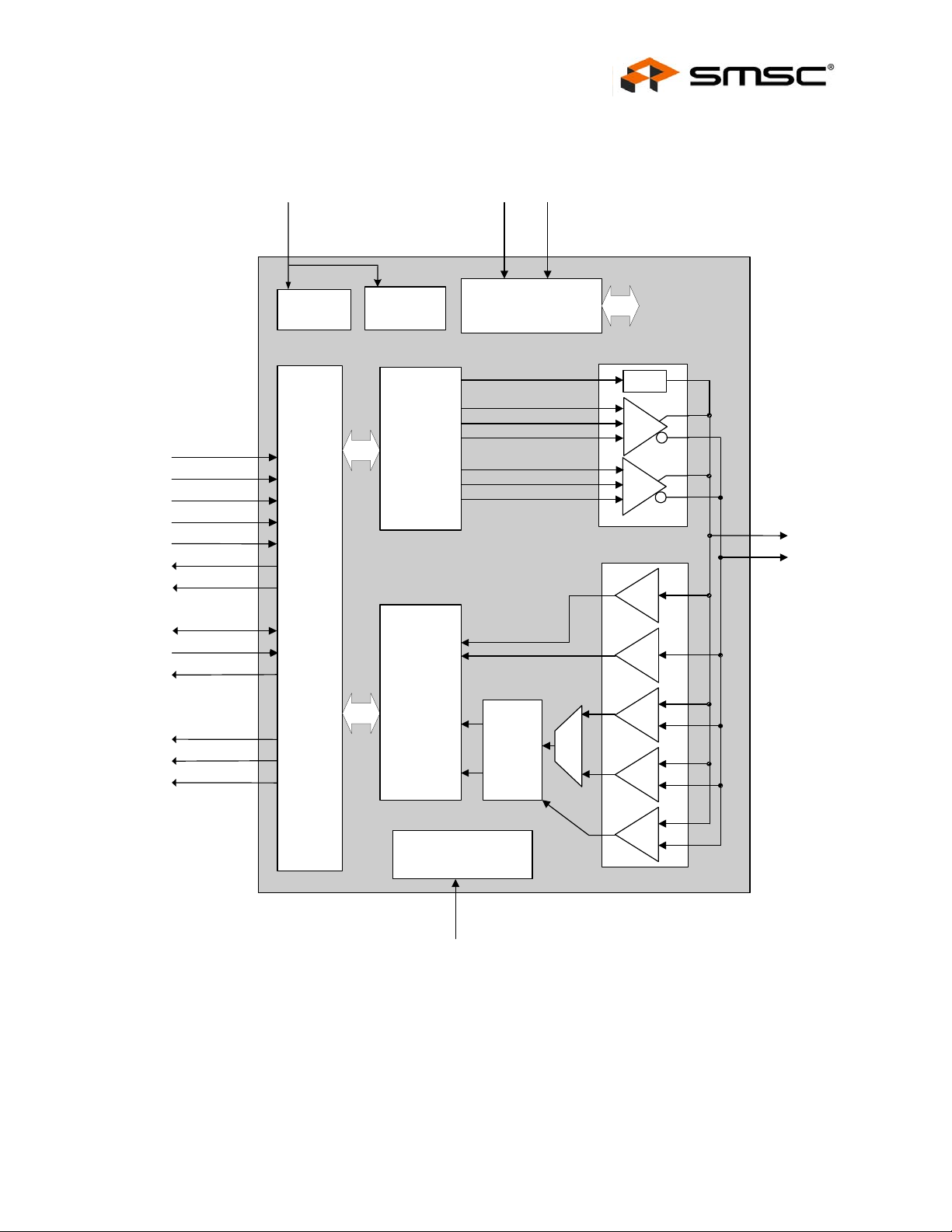
Chapter 2 Functional Block Diagram
XO
VDD3.3
XI
RESET
SUSPENDN
XCVRSELECT
TERMSELECT
:
M
D
[
1
O
P
O
E
LINESTATE[1:0]
CLKOUT
]
D
0
A
A
:
T
[
7
TXVALID
T
D
R
A
Y
E
X
R
D
A
I
V
L
X
R
E
A
I
V
C
X
T
R
R
X
R
O
E
R
PWR
Control
1.8V
Regulator
PLL and
XTAL OSC
TX
LOGIC
TX State
Machine
Parallel to
Serial
Conversion
Bit Stuff
NRZI
Encode
]
0
RPU_EN
VPO
VMO
OEB
HS_DATA
HS_DRIVE_ENABLE
HS_CS_ENABLE
1.5k
FS
TX
HS
TX
System
Clocking
TX
Ω
R
DP
DM
X
UTMI
Interface
RX
LOGIC
RX State
Machine
Serial to
Parallel
Conversion
Bit Unstuff
NRZI
Decode
VP
VM
Clock
Recovery Unit
Clock
and
Data
Recovery
Elasticity
Buffer
MUX
FS SE+
FS SE-
FS RX
HS RX
BIASING
Bandgap Voltage Reference
Current Reference
RBIAS
HS SQ
Figure 2.1 USB3280 Block Diagram
SMSC USB3280 7 Revision 1.5 (11-15-07)
DATASHEET
Page 8
R
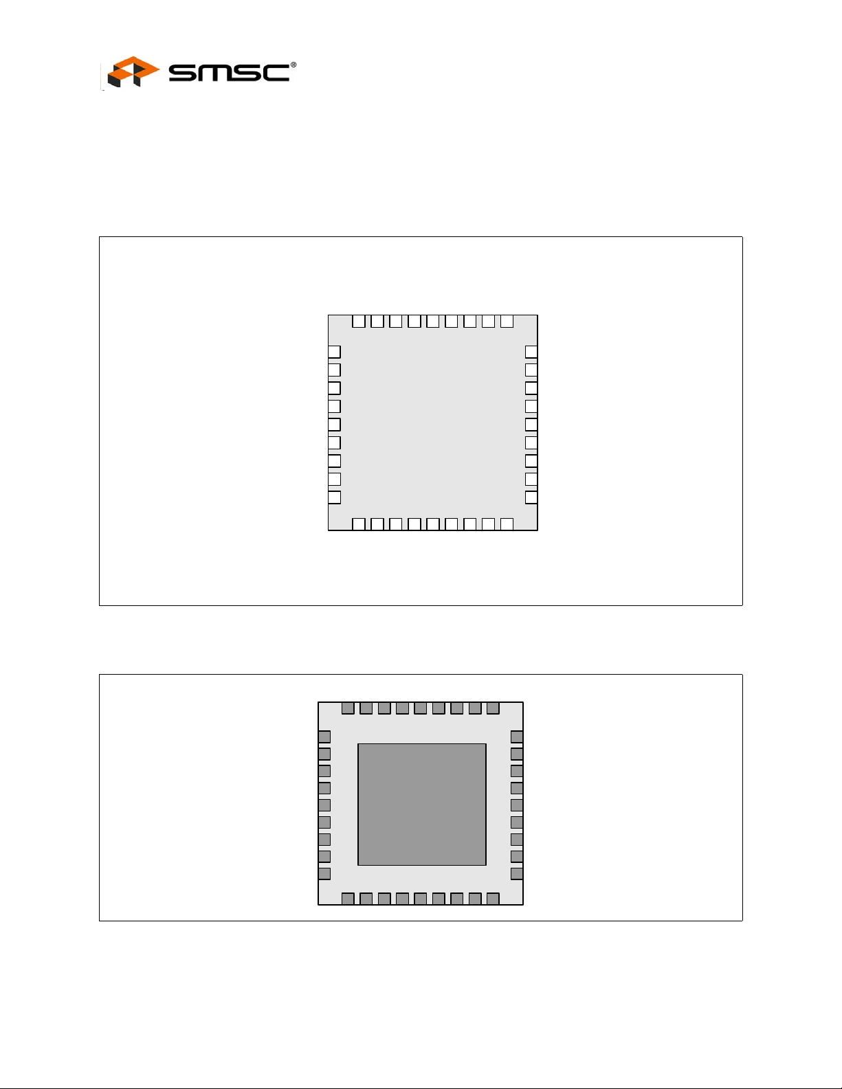
Chapter 3 Pinout
XCVRSELECT
TERMSELECT
TXREADY
SUSPENDN
TXVALID
RESET
VDD3.3
DP
DM
REG_EN
RBIAS
VDD3.3
VDDA1.8
XIXOVDD1.8
30
31
32
34
353633
1
2
3
4
5
6
7
8
9
USB2.0
USB3280
PHY IC
101112131415161718
Hi-Speed USB Device PHY with UTMI Interface
Datasheet
VDD3.3
RXERRO
28
29
27
26
25
24
23
22
21
20
19
RXVALID
DATA[0]
DATA[1]
DATA[2]
DATA[3]
DATA[4]
DATA[5]
DATA[6]
DATA[7]
VDD3.3
RXACTIVE
CLKOUT
OPMODE0
OPMODE1
LINESTATE1
Figure 3.1 USB3280 Pinout - Top View
EXPOSED
GND PAD
Figure 3.2 USB3280 Pinout - Bottom View
LINESTATE0
VDD1.8
VDD3.3
The flag of the QFN package must be connected to ground.
Revision 1.5 (11-15-07) 8 SMSC USB3280
DATASHEET
Page 9
Hi-Speed USB Device PHY with UTMI Interface
Datasheet
Chapter 4 Interface Signal Definition
T able 4.1 System Interface Signals
ACTIVE
NAME DIRECTION
LEVEL DESCRIPTION
RESET
(RST)
XCVRSELECT
(XSEL)
TERMSELECT
(TSEL)
SUSPENDN
(SPDN)
CLKOUT
(CLK)
OPMODE[1:0]
(OM1)
(OM0)
Input High Reset. Reset all state machines. After coming out of
reset, must wait 5 rising edges of clock before asserting
TXValid for transmit.
See Section 7.8.3
Input N/A Transceiver Select. This signal selects between the FS
and HS transceivers:
0: HS transceiver enabled
1: FS transceiver enabled.
Input N/A Termination Select. This signal selects between the FS
and HS terminations:
0: HS termination enabled
1: FS termination enabled
Input Low Suspend. Places the transceiver in a mode that draws
minimal power from supplies. Shuts down all blocks not
necessary for Suspend/Resume operation. While
suspended, TERMSELECT must always be in FS mode
to ensure that the 1.5kΩ pull-up on DP remains powered.
0: Transceiver circuitry drawing suspend current
1: Transceiver circuitry drawing normal current
Output Rising Edge System Clock. This output is used for clocking receive
and transmit parallel data at 60MHz.
Input N/A Operational Mode. These signals select between the
various operational modes:
[1] [0] Description
0 0 0: Normal Operation
0 1 1: Non-driving (all terminations removed)
1 0 2: Disable bit stuffing and NRZI encoding
1 1 3: Reserved
LINESTATE[1:0]
(LS1)
(LS0)
SMSC USB3280 9 Revision 1.5 (11-15-07)
Output N/A Line State. These signals reflect the current state of the
USB data bus in FS mode, with [0] reflecting the state of
DP and [1] reflecting the state of DM. When the device is
suspended or resuming from a suspended state, the
signals are combinatorial. Otherwise, the signals are
synchronized to CLKOUT.
[0] Description
[1]
0 0 0: SE0
0 1 1: J State
1 0 2: K State
1 1 3: SE1
DATASHEET
Page 10
NAME DIRECTION
Hi-Speed USB Device PHY with UTMI Interface
Datasheet
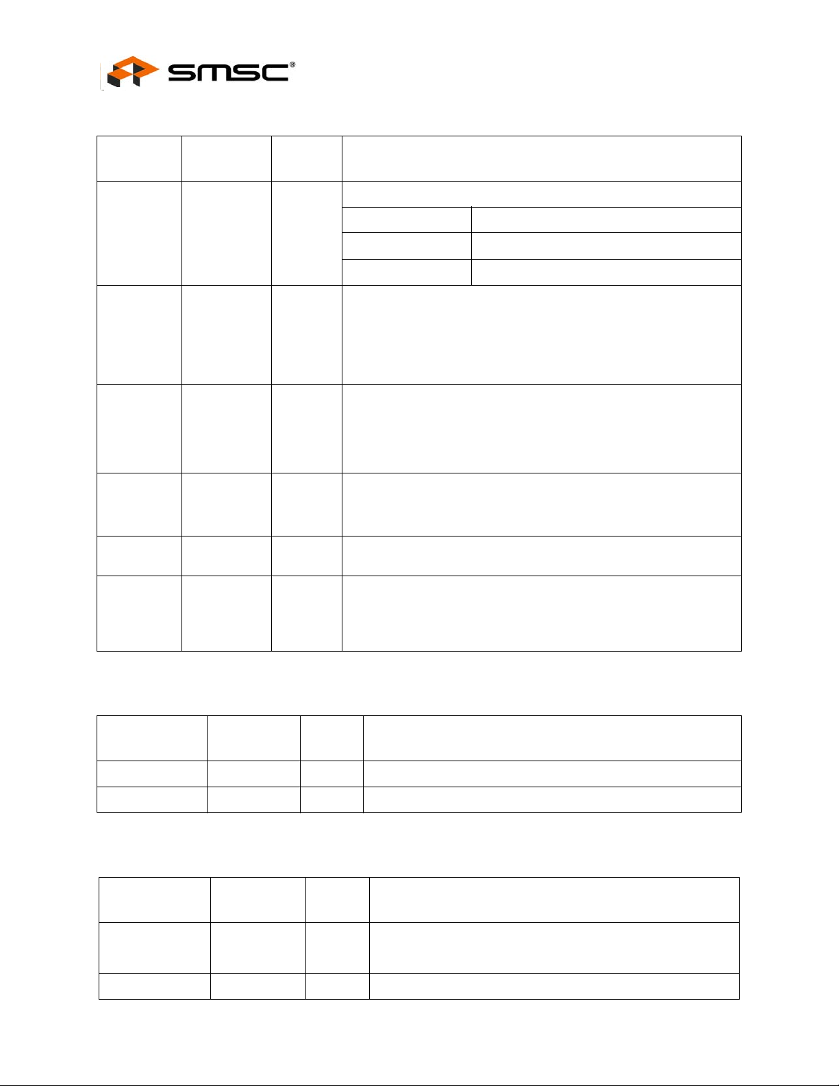
T ab le 4.2 Data Interface Signals
ACTIVE
LEVEL DESCRIPTION
DATA[7:0]
(D7)
.
.
.
(D0)
TXVALID
(TXV)
TXREADY
(TXR)
RXVALID
(RXV)
RXACTIVE
(RXA)
RXERROR
(RXE)
Bidirectional High Data bus. 8-bit Bidirectional mode.
TXVALID DATA[7:0]
0 output
1 input
Input High Transmit Valid. Indicates that the DATA bus is valid for transmit. The
assertion of TXVALID initiates the transmission of SYNC on the USB
bus. The negation of TXVALID initiates EOP on the USB.
Control inputs (OPMODE[1:0], TERMSELECT,XCVRSELECT) must
not be changed on the de-assertion or assertion of T XVALID. The
PHY must be in a quiescent state when these inputs are changed.
Output High Transmit Data Ready. If TXVALID is asserted, the SIE must always
have data available for clocking into the TX Holding Register on the
rising edge of CLKOUT. TXREADY is an acknowledgement to the
SIE that the transceiver has clocked the data from the bus and is
ready for the next transfer on the bus. If TXVALID is negated,
TXREADY can be ignored by the SIE.
Output High Receive Data Valid. Indicates that the DATA bus has received valid
data. The Receive Data Holding Register is full and ready to be
unloaded. The SIE is expected to latch the DATA bus on the rising
edge of CLKOUT.
Output High Receive Active. Indicates that the receive state machine has
detected Start of Packet and is active.
Output High Receive Error.
0: Indicates no error.
1: Indicates a receive error has been detected.
This output is clocked with the same timing as the rece ive DATA lines
and can occur at anytime during a transfer.
Table 4.3 USB I/O Signals
ACTIVE
NAME DIRECTION
DP I/O N/A USB Positive Data Pin.
DM I/O N/A USB Negative Data Pin.
NAME DIRECTION
RBIAS
(RB)
XI/XO Input N/A External crystal. 24MHz crystal connected from XI to XO.
Revision 1.5 (11-15-07) 10 SMSC USB3280
Input N/A External 1% bias resistor. Requires a 12kΩ resistor to ground.
LEVEL DESCRIPTION
Table 4.4 Biasing and Clock Oscillator Signals
ACTIVE
LEVEL DESCRIPTION
Used for setting HS transmit current level and on-chip
termination impedance.
DATASHEET
Page 11
Hi-Speed USB Device PHY with UTMI Interface
Datasheet
Table 4.5 Power and Ground Signals
ACTIVE
NAME DIRECTION
LEVEL DESCRIPTION
VDD3.3
(V33)
REG_EN
(REN)
VDD1.8
(V18)
VSS
(GND)
VDDA1.8
(V18A)
N/A N/A 3.3V Supply. Provides power for USB 2.0 Transceiver, UTMI+
Digital, Digital I/O, and Regulators.
Input High On-Chip 1.8V regulator enable. Connect to ground to disable
both of the on chip (VDDA1.8 and VDD1.8) regulators. When
regulators are disabled:
External 1.8V must be suppl ied to VDDA1.8 and VDD1.8 pins.
When the regulators are disabled, VDDA1.8 may be connected
to VDD1.8 and a bypass capacitor (0.1μF recommended)
should be connected to each pin.
The voltage at VD D3.3 must be at least 2.64V (0.8 * 3.3V)
before voltage is applied to VDDA1.8 and VDD1.8.
N/A N/A 1.8V Digital Supply. Supplied by On-Chip Regulator when
REG_EN is active. Low ESR 4.7uF minimum capacitor
requirement when using internal regulators. Do not connect
VDD1.8 to VDDA1.8 when using internal regulators. When the
regulators are disabled, VDD1.8 may be connected to VDD1.8A.
N/A N/A Common Ground.
N/A N/A 1.8V Analog Supply. Supplied by On-Chip Regulator when
REG_EN is active. Low ESR 4.7uF minimum capacitor
requirement when using internal regulators. Do not connect
VDD1.8A to VDD1.8 when using internal regulators. When the
regulators are disabled, VDD1.8A may be connected to VDD1.8.
SMSC USB3280 11 Revision 1.5 (11-15-07)
DATASHEET
Page 12
Chapter 5 Limiting Values
Table 5.1 Absolute Maximum Ratings
PARAMETER SYMBOL CONDITIONS MIN TYP MAX UNITS
Hi-Speed USB Device PHY with UTMI Interface
Datasheet
Maximum DP and DM
voltage to Ground
Maximum VDD1.8 and
VDDA1.8 voltage to Ground
Maximum 3.3V Supply
Voltage to Ground
Maximum I/O Voltage to
Ground
Storage Temperature T
V
MAX_5V
V
MAX_1.8V
V
MAX_3.3V
V
I
STG
-0.3 5.5 V
-0.3 2.5 V
-0.3 4.0 V
-0.3 4.0 V
-55 150
ESD PERFORMANCE
All Pins V
HBM
Human Body Model ±5 kV
LATCH-UP PERFORMANCE
All Pins I
LTCH_UP
EIA/JESD 78, Class II 150 mA
Note: In accordance with the Absolute Maximum Rating system (IEC 60134)
Table 5.2 Recommended Operating Conditions
PARAMETER SYMBOL CONDITIONS MIN TYP MAX UNITS
o
C
3.3V Supply Voltage
(VDD3.3 and VDDA3.3)
Input Voltage on Digital Pins V
Input Voltage on Analog I/O
Pins (DP, DM)
Ambient Temperature T
V
DD3.3
I
V
I(I/O)
A
3.0 3.3 3.6 V
0.0 V
0.0 V
-40 85
DD3.3
DD3.3
o
V
V
C
Table 5.3 Recommended External Clock Conditions
PARAMETER SYMBOL CONDITIONS MIN TYP MAX UNITS
System Clock Frequency XO driven by the external
clock; and no connection at XI
System Clock Duty Cycle XO driven by the external
45 50 55 %
24
(±100ppm)
MHz
clock; and no connection at XI
Revision 1.5 (11-15-07) 12 SMSC USB3280
DATASHEET
Page 13
Hi-Speed USB Device PHY with UTMI Interface
Datasheet
Chapter 6 Electrical Characteristics
Table 6.1 Electrical Characteristics: Supp ly Pins (Note 6.1)
PARAMETER SYMBOL CONDITIONS MIN TYP MAX UNITS
Unconfigured Current I
FS Idle Current I
FS Transmit Current I
FS Receive Current I
HS Idle Current I
HS Transmit Current I
HS Receive Current I
Low Power Mode I
AVG(UCFG)
AVG(FS)
AVG(FSTX)
AVG(FSRX)
AVG(HS)
AVG(HSTX)
AVG(HSRX)
DD(LPM)
Device Unconfigured 55 mA
FS idle not data transfer 55 mA
FS current during data
60.5 mA
transmit
FS current during data
57.5 mA
receive
HS idle not data transfer 60.6 mA
HS current during data
62.4 mA
transmit
HS current during data
61.5 mA
receive
VBUS 15kΩ pull-down and
83 uA
1.5kΩ pull-up resistor
currents not included.
Note 6.1 V
= 3.0 to 3.6V; VSS = 0V; TA = -40oC to 85oC; unless otherwise specified.
DD3.3
T able 6.2 DC Electrical Characteristics: Logic Pins (Note 6.2)
PARAMETER SYMBOL CONDITIONS MIN TYP MAX UNITS
Low-Level Input Voltage V
High-Level Input Voltage V
Low-Level Output Voltage V
High-Level Output Voltage V
Input Leakage Current I
IL
IH
OL
OH
LI
IOL = 8mA 0.4 V
IOH = -8mA V
V
SS
2.0 V
DD3.3
- 0.5
0.8 V
DD3.3
± 1 uA
V
V
Pin Capacitance Cpin 4 pF
Note 6.2 V
SMSC USB3280 13 Revision 1.5 (11-15-07)
= 3.0 to 3.6V; VSS = 0V; TA = -40oC to 85oC; unless otherwise specified.
DD3.3
DATASHEET
Page 14
Table 6.3 DC Electrical Character istics: Analog I/O Pins (DP/DM) (Note 6.3)
PARAMETER SYMBOL CONDITIONS MIN TYP MAX UNITS
FS FUNCTIONALITY
Input levels
Hi-Speed USB Device PHY with UTMI Interface
Datasheet
Differential Receiver Input
Sensitivity
Differential Receiver
Common-Mode Voltage
Single-Ended Receiver Low
Level Input Voltage
Single-Ended Receiver High
Level Input Voltage
Single-Ended Receiver
Hysteresis
Output Levels
Low Level Output Voltage V
High Level Output Voltage V
Termination
Driver Output Impedance for
HS and FS
Input Impedance Z
Pull-up Resistor Impedance Z
Pull-up Resistor Impedance Z
Termination Voltage For Pull-
up
Resistor On Pin DP
V
DIFS
V
CMFS
V
ILSE
V
IHSE
V
HYSSE
FSOL
FSOH
Z
HSDRV
INP
PU
PURX
V
TERM
| V(DP) - V(DM) | 0.2 V
0.8 2.5 V
0.8 V
2.0 V
0.050 0.150 V
Pull-up resistor on DP;
RL = 1.5kΩ to V
DD3.3
Pull-down resistor on DP,
2.8 3.6 V
0.3 V
DM;
RL = 15kΩ to GND
Steady state drive
40.5 45 49.5 Ω
(See Figure 6.1)
TX, RPU disabled 10 MΩ
Bus Idle 0.900 1.24 1.575 kΩ
Device Receiving 1.425 2.26 3.09 kΩ
3.0 3.6 V
HS FUNCTIONALITY
Input levels
HS Differential Input Sensitivity V
HS Data Signaling Common
Mode Voltage Range
HS Squelch Detection
Threshold (Differential)
DIHS
V
CMHS
V
HSSQ
| V(DP) - V(DM) | 100 mV
-50 500 mV
Squelch Threshold 100 mV
Unsquelch Threshold 150 mV
Output Levels
High Speed Low Level
Output Voltage (DP/DM
V
HSOL
45Ω load -10 10 mV
referenced to GND)
Revision 1.5 (11-15-07) 14 SMSC USB3280
DATASHEET
Page 15

Hi-Speed USB Device PHY with UTMI Interface
Datasheet
Table 6.3 DC Electrical Characteristics: Analog I/O Pins (DP/DM) (Note 6.3) (continued)
PARAMETER SYMBOL CONDITIONS MIN TYP MAX UNITS
High Speed High Level
Output Voltage (DP/DM
V
HSOH
45Ω load 360 440 mV
referenced to GND)
High Speed IDLE Level
Output Voltage (DP/DM
V
OLHS
45Ω load -10 10 mV
referenced to GND)
Chirp-J Output Voltage
(Differential)
V
CHIRPJ
HS termination resistor
disabled, pull-up resistor
700 1100 mV
connected. 45Ω load.
Chirp-K Output Voltage
(Differential)
V
CHIRPK
HS termination resistor
disabled, pull-up resistor
-900 -500 mV
connected. 45Ω load.
Leakage Current
OFF-State Leakage Current I
LZ
Port Capacitance
Transceiver Input Capacitance C
Note 6.3 V
= 3.0 to 3.6V; VSS = 0V; TA = -40oC to 85oC; unless otherwise specified.
DD3.3
IN
Pin to GND 5 10 pF
T able 6.4 Dynamic Characteristics: Analog I/O Pins (DP/DM) (Note 6.4)
PARAMETER SYMBOL CONDITIONS MIN TYP MAX UNITS
± 1 uA
FS Output Driver Timing
Rise Time T
Fall Time T
Output Signal Crossover
Voltage
Differential Rise/Fall Time
Matching
HS Output Driver Timing
Differential Rise Time T
Differential Fall Time T
Driver Waveform
Requirements
High Speed Mode Timing
Receiver Waveform
Requirements
Data Source Jitter and
Receiver Jitter Tolerance
CL = 50pF; 10 to 90% of
|VOH - VOL|
CL = 50pF; 10 to 90% of
|VOH - VOL|
Excluding the first
transition from IDLE state
V
FSR
FFF
CRS
FRFM Excluding the first
transition from IDLE state
HSR
HSF
Eye pattern of T emplate 1
in USB 2.0 specification
Eye pattern of T emplate 4
in USB 2.0 specification
Eye pattern of T emplate 4
in USB 2.0 specification
420ns
420ns
1.3 2.0 V
90 111.1 %
500 ps
500 ps
See
Figure 6.2
See
Figure 6.2
See
Figure 6.2
Note 6.4 V
SMSC USB3280 15 Revision 1.5 (11-15-07)
= 3.0 to 3.6V; VSS = 0V; TA = -40oC to 85oC; unless otherwise specified.
DD3.3
DATASHEET
Page 16

Hi-Speed USB Device PHY with UTMI Interface
T able 6.5 Dynamic Characteristics: Digital UTMI Pins (Note 6.5)
PARAMETER SYMBOL CONDITIONS MIN TYP MAX UNITS
UTMI Timing
Datasheet
DATA[7:0] T
RXVALID
RXACTIVE
RXERROR
LINESTATE[1:0]
TXREADY
DATA[7:0] T
TXVALID
OPMODE[1:0]
XCVRSELECT
TERMSELECT
DATA[7:0] T
TXVALID
OPMODE[1:0]
XCVRSELECT
TERMSELECT
PD
SU
H
Output Delay. Measured
from PHY output to the
rising edge of CLKOUT
Setup Time. Measured
from PHY input to the
rising edge of CLKOUT.
Hold time. Measured from
the rising egde of
CLKOUT to the PHY input
signal edge.
25ns
5ns
0ns
Note 6.5 V
= 3.0 to 3.6V; VSS = 0V; TA = -40oC to 85oC; unless otherwise specified.
DD3.3
6.1 Driver Characteristics of Full-Speed Drivers in High-Speed Capable Transceivers
The USB3280 uses a differential output driver to drive the USB data signal onto the USB cable.
Figure 6.1 Full-Speed Driver VOH/IOH Characteristics for High-speed Capable Transceiveron page 17
shows the V/I characteristics for a full-speed driver which is part of a high-speed capable transceiver.
The normalized V/I curve for the driver must fall entirely inside th e shaded region. The V/I region is
bounded by the minimum driver impedance above (40.5 Ohm) and the maximum driver impedance
below (49.5 Ohm). The output voltage must be within 10mV of ground when no current is flowin g in
or out of the pin.
Revision 1.5 (11-15-07) 16 SMSC USB3280
DATASHEET
Page 17

Hi-Speed USB Device PHY with UTMI Interface
Datasheet
Drive High
Iout
(mA)
OH|
-6.1 * |V
Slope = 1/49.5 Ohm
-10.71 * |V
Figure 6.1 Full-Speed Driver VOH/IOH Characte ristics for High-speed Capable Transceiver
OH|
0
0
Test Limit
0.566*VOH
Vout (Volts)
Slope = 1/40.5 Ohm
0.698*VOH
Drive Low
I
out
(mA)
10.71 * |VOH|
Slope = 1/40.5 Ohm
Test Limit
VOH
22
Slope = 1/49.5 Ohm
0
0
Figure 6.2 Full-Speed Driver VOL/IOL Characteristics for High-speed Capable Transceiver
SMSC USB3280 17 Revision 1.5 (11-15-07)
1.09V 0.434*V
OH
VOH
Vout (Volts)
DATASHEET
Page 18

6.2 High-speed Signaling Eye Patterns
High-speed USB signals are characterized using eye patterns. For measuring the eye patterns 4
points have been defined (see Figure 6.3). The Universal Serial Bus Specification Rev.2.0 defines the
eye patterns in several ‘templates’. The two templates that are relevant to the PHY are shown below.
TP1 TP2 TP3 TP4
Hi-Speed USB Device PHY with UTMI Interface
Datasheet
Traces Traces
Transceiver
Connector
Hub Circuit Board
USB Cable
A
Connector
Figure 6.3 Eye Pattern Measurement Planes
B
Transceiver
Device Circuit Board
Revision 1.5 (11-15-07) 18 SMSC USB3280
DATASHEET
Page 19

Hi-Speed USB Device PHY with UTMI Interface
Datasheet
The eye pattern in Figure 6.4 defines the transmit waveform requirements for a hub (measured at TP2
of Figure 6.3) or a devi ce without a captive cable (measured at TP3 of Figure 6.3). The corresponding
signal levels and timings are given in table below. Time is specified as a percentage of the unit interval
(UI), which represents the nominal bit duration for a 480 Mbit/s transmission rate.
Level 1
400mV
Point 4 Point 3
Differential
Point 2
Point 6 Point 5
100%
Level 2
0%
Point 1
Unit Interval
Figure 6.4 Eye Pattern for Transmit Waveform and Eye Pattern Definition
VOLTAGE LEVEL (D+, D-) TIME (% OF UNIT INTERVAL)
Level 1 525mV in UI following a transition,
N/A
475mV in all others
Level 2 -525mV in UI following a transition,
N/A
-475mV in all others
Point 1 0V 7.5% UI
0 Volts
Differential
-400mV
Differential
Point 2 0V 92.5% UI
Point 3 300mV 37.5% UI
Point 4 300mV 62.5% UI
Point 5 -300mV 37.5% UI
Point 6 -300mV 62.5% UI
SMSC USB3280 19 Revision 1.5 (11-15-07)
DATASHEET
Page 20

Hi-Speed USB Device PHY with UTMI Interface
Datasheet
The eye pattern in Figure 6.5 defines the receiver sen sitivity requirements for a hub (signal applied at
test point TP2 of Figure 6.3) or a device without a captive cable (signal applied at test point TP3 of
Figure 6.3). The corresponding signal levels and timings are gi ven in the table below. Timings are
given as a percentage of the unit interval (UI), which represents the nominal bit duration for a 480
Mbit/s transmission rate.
Level 1
400mV
Differential
Point 3 Point 4
Point 1
Point 5
Level 2
0%
Point 2
Point 6
100%
Figure 6.5 Eye Pattern for Receive Waveform and Eye Pattern Definition
VOLTAGE LEVEL (D+, D-) TIME (% OF UNIT INTERVAL)
Level 1 575mV N/A
Level 2 -575mV N/A
Point 1 0V 1 5% UI
Point 2 0V 8 5% UI
Point 3 150mV 35% UI
0 Volts
Differential
-400mV
Differential
Point 4 150mV 65% UI
Point 5 -150mV 35% UI
Point 6 -150mV 65% UI
Revision 1.5 (11-15-07) 20 SMSC USB3280
DATASHEET
Page 21

Hi-Speed USB Device PHY with UTMI Interface
Datasheet
Chapter 7 Functional Overview
Figure 2.1 on page 7 shows the functional b lock diagram of the USB3280. Each of the functions is
described in detail below.
7.1 Modes of Operation
The USB3280 supports an 8-bit bi-directional parallel interface.
CLKOUT runs at 60MHz
The 8-bit data bus (DATA[7:0]) is used for transmit when TXVALID = 1
The 8-bit data bus (DATA[7:0]) is used for receive when TXVALID = 0
7.2 System Clocking
This block connects to either an external 24MHz crystal or an external clock source and generate s a
480MHz multi-phase clock. The clock is used in the CRC block to over-sample the incoming received
data, resynchronize the transmit data, and is divided down to 60MHz (CLKOUT) which acts as the
system byte clock. The PLL block also outputs a clock valid signal to the other parts of the transceiver
when the clock signal is stable. All UTMI signals are synchronized to the CLKOUT output. The
behavior of the CLKOUT is as follows:
Produce the first CLKOUT transition no later than 5.6ms after negation of SUSPENDN. The
CLKOUT signal frequency error is less than 10% at this time.
The CLKOUT signal will fully meet the required accuracy o f ±500ppm no la ter than 1.4ms after th e
first transition of CLKOUT.
In HS mode there is one CLKOUT cycle per byte time. The frequency of CLKOUT does not change
when the PHY is switched between HS to FS modes. In FS mode there are 5 CLKOUT cycles per FS
bit time, typically 40 CLKOUT cycles per FS byte time. If a received byte contains a stuffed bit then
the byte boundary can be stretched to 45 CLKOUT cycles, and two stuffed bits would result in a 50
CLKOUT cycles.
Figure 7.1 shows the relationship between CLKOUT and the transmit data transfer signals in FS mode.
TXREADY is only asserted for one CLKOUT per byte time to signal the SIE that the data on the DATA
lines has been read by the PHY. The SIE may hold the data on the DATA lines for the duration of the
byte time. Transitions of TXVALID must meet the defined setup and hold times relative to CLKOUT.
Figure 7.1 FS CLK Relationship to Transmit Data and Control Signals
SMSC USB3280 21 Revision 1.5 (11-15-07)
DATASHEET
Page 22

Hi-Speed USB Device PHY with UTMI Interface
Datasheet
Figure 7.2 shows the relationship between CLKOUT and t he receive data control signals in FS mode.
RXACTIVE "frames" a packet, transitioning only at the beginning and end of a packet. However
transitions of RXVALID may take place any time 8 bits of data are available. Figure 7.1 al so shows
how RXVALID is only asserted for one CLKOUT cycle per byte time even though the data may be
presented for the full byte time. The XCVRSELECT signal determines whether the HS or FS timing
relationship is applied to the data and control signals.
Figure 7.2 FS CLK Relationship to Receive Data and Control Signals
7.3 Clock and Data Recovery Circuit
This block consists of the Clock and Data Recovery Circuit and the Elasticity Buffer. The Elasticity
Buffer is used to compensate for differences between the transmitting and receiving clock domains.
The USB 2.0 specification defines a maximum clock error o f ±1000ppm of drift.
7.4 TX Logic
This block receives parallel data bytes placed on the DATA bus and performs the necessary transmit
operations. These operations include parallel to serial conversion, bit stuffing and NRZI encoding.
Upon valid assertion of the proper TX control lines by the SIE and TX State Machine, the TX LOGIC
block will synchronously shift, at either the FS or HS rate, the data to the FS/HS TX block to be
transmitted on the USB cable. Data transmit timing is shown in Figure 7.3.
Figure 7.3 Transmit Timing for a Data Packet
Revision 1.5 (11-15-07) 22 SMSC USB3280
DATASHEET
Page 23

Hi-Speed USB Device PHY with UTMI Interface
Datasheet
The behavior of the Transmit State Machine is described below.
Asserting a RESET forces the transmit state machine into the Reset state which negates
TXREADY. When RESET is negated the transmit state machine will enter a wait state.
The SIE asserts TXVALID to begin a transmission.
After the SIE asserts TXVALID it can assume that the transmission has started when it detects
TXREADY has been asserted.
The SIE must assume that t he USB3280 has consumed a data byte if TXREADY and TXVALID
are asserted on the rising edge of CLKOUT.
The SIE must have valid packet information (PID) asserted on the DATA bus coi ncident with the
assertion of TXVALID.
TXREADY is sampled by the SIE on the rising edge of CLKOUT.
The SIE negates TXVALID to complete a packet. Once negated, the transmit logic will never
reassert TXREADY until after the EOP has been generated. (TXREADY will not re-assert until
TXVALD asserts again.
The USB3280 is ready to transmit another packet immediately, however the SIE must conform to
the minimum inter-packet delays identified in the USB 2.0 specification.
7.5 RX Logic
This block receives serial data from the CRC block and processes it to be transferred to the SIE on
the DATA bus. The processing involved includes NRZI decoding, bit unstuffing, and serial to parallel
conversion. Upon valid assertion of the proper RX control lines by the RX State Machine, the RX Logic
block will provide bytes to the DATA bus as shown in the figures below. The behavior of the Receive
State Machine is described below.
Figure 7.4 Receive Timing for Data with Unstuffed Bits
The assertion of RESET will force the Receive State Machine into the Reset state. The Reset state
deasserts RXACTIVE and RXVALID. When the RESET signal is deasserted the Receive State
Machine enters the RX Wait state and starts looking for a SYNC pattern on the USB. When a SYNC
pattern is detected the state machine will enter the Strip SYNC state and assert RXACTIVE. The length
of the received Hi-Speed SYNC pattern varies and can be up to 32 bits long or as short as 12 bits
long when at the end of five hubs. As a result, the state machine may remain in the Strip SYNC state
for several byte times before capturing the first byte of data and entering the RX Data state.
After valid serial data is received, the state machine enters the RX Data state, where the data is loaded
into the RX Holding Register on the rising edge of CLKOUT and RXVALID is asserted. The SIE must
clock the data off the DATA bus on the next rising edge of CLKOUT. If OPMODE = Normal, then
stuffed bits are stripped from the data stream. Each time 8 stuffed bits are accumulated the state
machine will enter the RX Data Wait state, negating RXVALID thus skipping a byte time.
SMSC USB3280 23 Revision 1.5 (11-15-07)
DATASHEET
Page 24

Hi-Speed USB Device PHY with UTMI Interface
Datasheet
When the EOP is detected the state machine will enter the St rip EO P state and negate RXACTIVE
and RXVALID. After the EOP has been stripped the Receive State Machine will reenter the RX Wait
state and begin looking for the next packet.
The behavior of the Receive State Machine is described below:
RXACTIVE and RXREADY are sampled on the rising edge of CLKOU T.
In the RX Wait state the receiver is always looking for SYNC.
The USB3280 asserts RXACTIVE when SYNC is detected (Strip SYNC state).
The USB3280 negates RXACTIVE when an EOP is detected and the elasticity buffer is empty
(Strip EOP state).
When RXACTIVE is asserted, RXVALID will be asserted if the RX Holding Register is full.
RXVALID will be negated if the RX Holding Register was not loaded during the previous byte time.
This will occur if 8 stuffed bits have been accumulated.
The SIE must be ready to consume a data byte if RXACTIVE and RXVALID are asserted (RX Data
state).
Figure 7.5 shows the timing relati onship between the received data (DP/DM), RXVALID,
RXACTIVE, RXERROR and DATA signals.
Notes:
The USB 2.0 Transceiver does NOT decode Packet ID's (PIDs). They are passed to the SIE for
decoding.
Figure 7.5, Figure 7.6 and Figure 7.7 are timing examples of a HS/FS PHY when it is in HS mode.
When a HS/FS PHY is in FS Mode there are approximately 40 CLKOUT cycles every byte time .
The Receive State Machine assumes that the SIE captures the data on the DATA bus if RXACTIVE
and RXVALID are asserted. In FS mode, RXVALID will only be asserted for one CLKOUT per byte
time.
In Figure 7.5, Figure 7.6 and Figure 7.7 the SYNC pattern on DP/DM i s shown as one byte long.
The SYNC pattern received by a device can vary in length. These figures assume that all but the
last 12 bits have been consumed by the hubs between the device and the host controller.
Figure 7.5 Receive Timing for a Handshake Packet (n o CRC)
Revision 1.5 (11-15-07) 24 SMSC USB3280
DATASHEET
Page 25

Hi-Speed USB Device PHY with UTMI Interface
Datasheet
Figure 7.6 Receive Timing for Setup Packet
Figure 7.7 Receive Timing for Data Packet (with CRC-16)
The receivers connect directly to the USB cable. The block contains a separate differential receiver
for HS and FS mode. Depending on the mode, the selected receiver provides the serial data stream
through the mulitplexer to the RX Logic block. The FS mode section of the FS/HS RX block also
consists of a single-ended receiver on each of the data lines to determine the correct FS LINESTATE.
For HS mode support, the FS/HS RX block contains a squelch circuit to insure that noise is never
interpreted as data.
SMSC USB3280 25 Revision 1.5 (11-15-07)
DATASHEET
Page 26

7.6 USB 2.0 Transceiver
The SMSC Hi-Speed USB 2.0 Transceiver consists of the High Speed and Full Speed Transceivers,
and the Termination resistors.
7.6.1 High Speed and Full Speed Transceivers
The USB3280 transceiver meets all requirements in the USB 2.0 specification.
The receivers connect directly to the USB cable. This block contains a separate differential receiver
for HS and FS mode. Depending on the mode, the selected receiver provides the serial data stream
through the multiplexer to the RX Logic block. The FS mode section of the FS/HS RX block also
consists of a single-ended receiver on each of the data lines to determine the correct FS linestate. For
HS mode support, the FS/HS RX block contains a squelch circuit to insure that noise is never
interpreted as data.
The transmitters connect directly to the USB cable. The block contains a separate differential FS and
HS transmitter which receive encoded, bit stuffed, serialized data from the TX Logic block and transmit
it on the USB cable.
7.6.2 Termination Resistors
The USB3280 transceiver fully integrates all of the USB termination resistors. The USB3280 includes
the 1.5kΩ pull-up resistor on DP. In addition the 45Ω high speed termination resistors are also
integrated. These integrated resistors require no tuning or trimming. The state of the resistors is
determined by the operating mode of the PHY. The possible valid resistor combinations are shown in
Table 7.1.
RPU_DP_EN activates the 1.5kΩ DP pull-up resistor
HSTERM_EN activates the 45Ω DP and DM high speed termi nation resistors
Hi-Speed USB Device PHY with UTMI Interface
Datasheet
Table 7.1 DP/DM Termination vs. Sig naling Mode
OPMODE[1:0]
RESISTOR
SETTINGS
RPU_DP_EN
UTMI+ INTERFACE SETTINGS
SIGNALING MODE
Tri-State Drivers Xb Xb 01 b 0b 0b
Power-up 1b 0b 00b 0b 0b
Peripheral Chirp 0b 1b 10b 1b 0b
Peripheral HS 0b 0b 00b 0b 1b
Peripheral FS 1b 1b 00b 1b 0b
Peripheral HS/FS Suspend 1b 1b 00b 1b 0b
Peripheral HS/FS Resume 1b 1b 10b 1b 0b
Peripheral Test J/Test K 0b 0b 10b 0b 1b
XCVRSELECT
TERMSELECT
HSTERM_EN
Revision 1.5 (11-15-07) 26 SMSC USB3280
DATASHEET
Page 27

Hi-Speed USB Device PHY with UTMI Interface
Datasheet
7.6.3 Bias Generator
This block consists of an internal bandgap reference circuit used fo r generating the high speed driver
currents and the biasing of the analog circuits. This block requires an external 12kΩ, 1% tolerance,
external reference resistor connected from RBIAS to ground.
7.7 Crystal Oscillator and PLL
The USB3280 uses an internal crystal driver and PLL sub-system to provide a clean 480MHz reference
clock that is used by the PHY during both transmit and receive. The USB328 0 requires a clean 24MHz
crystal or clock as a frequency reference. If the 24MHz reference is noisy or off frequency the PHY
may not operate correctly.
The USB3280 can use either a crystal or an external clock oscillator for the 24MHz reference. The
crystal is connected to the XI and XO pins as shown in the application di agram, Figure 8.9. If a clock
oscillator is used the clock should be connected to the XI input and the XO pin left floating. When a
external clock is used the XI pin is designed to be driven with a 0 to 3.3 volt signal. Wh en using an
external clock the user needs to take care to ensure the external clock source is clean enough to not
degrade the high speed eye performance.
Once, the 480MHz PLL has locked to the correct fr equency it will drive the CLKOUT pin with a 60MHz
clock.
7.8 Internal Regulators and POR
The USB3280 includes an integrated set of built in power management functions. These power
management features include a POR generation and allow the USB3 280 to be powered from a single
3.3 volt power supply. This reduces the bill of materials and simplifies product design.
7.8.1 Internal Regulators
The USB3280 has two integrated 3.3 volt to 1.8 volt regulators. These regulators require an e xternal
4.7uF +/-20% low ESR bypass capacitor to ensure stability. X5R or X7R ceramic capacitors are
recommended since they exhibit an ESR lower than 0.1 ohm at frequencies greater than 10kHz.
The two regulator outputs, which require bypass capacitors, are the pins labeled VDDA1.8 and
VDD1.8. Each pin requires a 4.7uF bypass capacitor placed as close to the pin as possible.
Note: The USB3280 regulators are designed to generate a 1.8 volt supply for the USB3280 only.
Using the regulators to provide current for other circuits is not recommended and SMSC does
not guarantee USB performance or regulator stability.
7.8.2 Power On Reset (POR)
The USB3280 provides an internal POR circuit that generates a reset pulse once the PHY supplies
are stable.
7.8.3 Reset Pin
The UTMI+ Digital can be reset at any time with the RESET pin. The RESET pin of the USB3280 may
be asynchronously asserted and de-asserted so long as it is held in the asserted state continuo usly
for a duration greater than one CLKOUT cycle. The RESET input may be asserted when the USB32 80
CLKOUT signal is not active (i.e. in the suspend state caused by asserting the SUSPENDN input) but
reset must only be de-asserted when the USB3280 CLKOUT signal is active and the RESET has been
held asserted for a duration greater than one CKOUT clock cycle . No other PHY digital input signals
may change state for two CLKOUT clock cycles after the de-assertion of the reset signal.
SMSC USB3280 27 Revision 1.5 (11-15-07)
DATASHEET
Page 28

Chapter 8 Application Notes
The following sections consist of select functional explanations to aid in i mplementing the USB3280
into a system. For complete description and specifications consult the USB 2.0 Transceiver Macrocell
Interface Specification and Universal Serial Bus Specification Revision 2.0 .
8.1 Linestate
The voltage thresholds that the LINESTATE[1:0] signals use to reflect the state of DP and DM depend
on the state of XCVRSELECT. LINESTATE[1:0] uses HS thresholds when the HS transceiver is
enabled (XCVRSELECT = 0) and FS thresholds when the FS transceiver is enabled (XCVRSELECT
= 1). There is not a concept of variable single-ended thresholds in the USB 2.0 specification for HS
mode.
The HS receiver is used to detect Chirp J or K, where the output of the HS receiver is always quali fied
with the Squelch signal. If squelched, the output of the HS receiver is ignored. In the USB32 80, as
an alternative to using variable thresholds for the single-ended receivers, the following approach is
used.
Table 8.1 Linestate States
Hi-Speed USB Device PHY with UTMI Interface
Datasheet
STATE OF DP/DM LINES
LINESTATE[1:0]
0 0 SE0 Squelch Squelch
0 1 J !Squelch !Squelch &
1 0 K Invalid !Squelch &
1 1 SE1 Invalid Invalid
In HS mode, 3ms of no USB activity (IDLE state) signals a reset. The SIE monitors LINESTATE[1:0]
for the IDLE state. To minimize transitions on LINESTATE[1:0] while in HS mode, the presence of
!Squelch is used to force LINESTATE[1:0] to a J state.
FULL SPEED
XCVRSELECT =1
TERMSELECT=1
HIGH SPEED
XCVRSELECT =0
TERMSELECT=0
CHIRP MODE
XCVRSELECT =0
TERMSELECT=1LS[1] LS[0]
HS Differential Receiver
Output
!HS Differential Receiver
Output
Revision 1.5 (11-15-07) 28 SMSC USB3280
DATASHEET
Page 29

Hi-Speed USB Device PHY with UTMI Interface
Datasheet
8.2 OPMODES
The OPMODE[1:0] pins allow control of the operating modes.
Table 8.2 Operational Modes
MODE[1:0] STATE# STATE NAME DESCRIPTION
00 0 Normal Operation Transceiver operates with normal USB data encoding and
01 1 Non-Driving Allows the transceiver logic to support a soft disconnect feature
10 2 Disable Bit Stuffing
and NRZI encoding
11 3 Reserved N/A
The OPMODE[1:0] signals are normally changed only when the transmitter and the receiver are
quiescent, i.e. when entering a test mode or for a device initiated resume.
When using OPMODE[1:0] = 10 (state 2), OPMODES are set, and then 5 60MHz clocks later,
TXVALID is asserted. In this case, the SYNC and EOP patterns are not transmitted.
The only exception to this is when OPMODE[1:0] is se t to state 2 while TXVALID has been asserted
(the transceiver is transmitting a packet), in order to flag a transmission error. In this case, the
USB3280 has already transmitted the SYNC pattern so upon negation of TXVALID the EOP must also
be transmitted to properly terminate the packet. Changing the OPMODE[1:0] signals under all other
conditions, while the transceiver is transmitting or receiving data will generate und efined results.
Under no circumstances should the device controller change OPMODE while the DP/DM lines are still
transmitting or unpredictable changes on DP/DM are likely to occur. The same applies for
TERMSELECT and XCVRSELECT.
decoding
which tri-states both the HS and FS transmitters, and removes
any termination from the USB making it appear to an upstream
port that the device has been disconnected from the bus
Disables bitstuffing and NRZI encoding logic so that 1's loaded
from the DATA bus become 'J's on the DP/DM and 0's become
'K's
8.3 Test Mode Support
Table 8.3 USB 2.0 Test Mode s
USB3280 SETUP
XCVRSELECT &
USB 2.0 TEST MODES
SE0_NAK State 0 No transmit HS
J State 2 All '1's HS
K State 2 All '0's HS
Test_Packet State 0 Test Packet data HS
SMSC USB3280 29 Revision 1.5 (11-15-07)
OPERATIONAL MODE SIE TRANSMITTED DATA
DATASHEET
TERMSELECT
Page 30

8.4 SE0 Handling
For FS operation, IDLE is a J state on the bus. SE0 is used as part of the EOP or to indicate reset.
When asserted in an EOP, SE0 is never asserted for more than 2 bit times. The assertion of SE0 for
more than 2.5us is interpreted as a reset by the device operating in FS mode.
For HS operation, IDLE is a SE0 state on the bus. SE0 is also used to reset a HS device. A HS
device cannot use the 2.5us assertion of SE0 (as defined for FS opera tion) to indicate reset since the
bus is often in this state between packets. If no bus activity (IDLE) is detected for more than 3ms, a
HS device must determine whether the downstream facing port is signaling a suspend or a reset. The
following section details how this determination is made. If a reset is signaled, the HS device will then
initiate the HS Detection Handshake protocol.
8.5 Reset Detection
If a device in HS mode detects bus inactivity for more than 3ms (T1), it reverts to FS mode. This
enables the FS pull-up on the DP line i n an attempt to assert a continuous FS J state on the bus. The
SIE must then check LINESTATE for the SE0 condition. If SE0 is asserted at time T2, then the
upstream port is forcing the reset state to the device (i.e., a Driven SE0). The device will then initiate
the HS detection handshake protocol.
Hi-Speed USB Device PHY with UTMI Interface
Datasheet
Figure 8.1 Reset Timing Behavio r (HS Mode)
Table 8.4 Reset Timing Values (HS Mode)
TIMING
PARAMETER DESCRIPTION VALUE
HS Reset T0 Bus activity ceases, signal ing either a reset
or a SUSPEND.
T1 Earliest time at which the device may place
itself in FS mode after bus activity stops.
T2 SIE samples LINESTATE. If LINESTATE =
SE0, then the SE0 on the bus is due to a
Reset state. The device now enters the HS
Detection Handshake protocol.
Revision 1.5 (11-15-07) 30 SMSC USB3280
0 (reference)
HS Reset T0 + 3. 0ms < T1 < HS Reset T0
+ 3.125ms
T1 + 100µs < T2 <
T1 + 875µs
DATASHEET
Page 31

Hi-Speed USB Device PHY with UTMI Interface
Datasheet
8.6 Suspend Detection
If a HS device detects SE0 asserted on the bus for more than 3ms (T1), it reverts to FS mode. This
enables the FS pull-up on the DP line i n an attempt to assert a continuous FS J state on the bus. The
SIE must then check LINESTATE for the J condition. If J is asserted at time T2, then the upstream
port is asserting a soft SE0 and the USB is in a J state indicating a suspend condition. By time T4
the device must be fully suspended.
Figure 8.2 Suspend Timing Behavior (HS Mo de)
T able 8.5 Suspend Timing Values (HS Mode)
TIMING
PARAMETER DESCRIPTION VALUE
HS Reset T0 End of last bus activity, signaling either a reset
or a SUSPEND.
T1 The time at which the device must place itself
in FS mode after bus activity stops.
T2 SIE samples LINESTATE. If LINESTATE = 'J',
then the initial SE0 on the bus (T0 - T1) had
been due to a Suspend state and the SIE
remains in HS mode.
T3 The earliest time where a device can issue
Resume signaling.
T4 The latest time that a device must actually be
suspended, drawing no more than the
suspend current from the bus.
0 (reference)
HS Reset T0 + 3. 0ms < T1 < HS Reset T0
+ 3.125ms
T1 + 100 µs < T2 <
T1 + 875µs
HS Reset T0 + 5ms
HS Reset T0 + 10ms
SMSC USB3280 31 Revision 1.5 (11-15-07)
DATASHEET
Page 32

8.7 HS Detection Handshake
The High Speed Detection Handshake process is entered from one of three states: suspend, active
FS or active HS. The downstream facing port asserting an SE0 state on the bus initiates the HS
Detection Handshake. Depending on the initial state, an SE0 condition can be asserted from 0 to 4
ms before initiating the HS Detection Handshake. These states are described in the USB 2.0
specification.
There are three ways in which a device may enter the HS Handshake Detection process:
1. If the device is suspended and it detects an SE0 state on the bus it may immediately enter the HS
handshake detection process.
2. If the device is in FS mode and an SE0 state is detected for more than 2.5µs. it may enter the HS
handshake detection process.
3. If the device is in HS mode and an SE0 state is detected for more than 3.0ms. it may enter the
HS handshake detection process. In HS mode, a device must first determine whether the SE0 state
is signaling a suspend or a reset condition. To do this the device reverts to FS mode by placing
XCVRSELECT and TERMSELECT into FS mode. The device must not wait more than 3.125ms
before the reversion to FS mode. After reverting to FS mode, no less than 100µs and no more
than 875µs later the SIE must check the LINESTATE signals. If a J state is detected the device
will enter a suspend state. If an SE0 state is detected, then the device will enter the HS H andshake
detection process.
Hi-Speed USB Device PHY with UTMI Interface
Datasheet
In each case, the assertion of the SE0 state on the bus initiates the reset. The minimu m reset interval
is 10ms. Depending on the previous mode that the bus was in, the delay between the initial asserti on
of the SE0 state and entering the HS Handshake detection can be from 0 to 4ms.
This transceiver design pushes as much of the responsibility for timing events on to the SIE as
possible, and the SIE requires a stable CLKOUT signal to perform accurate timing. In case 2 and 3
above, CLKOUT has been running and is stable, however in case 1 the USB3280 is reset from a
suspend state, and the internal oscillator and clocks of the transceiver are assumed to be powered
down. A device has up to 6ms after the release of SUSPENDN to assert a minimum of a 1ms Chirp K.
8.8 HS Detection Handshake – FS Downstream Facing Port
Upon entering the HS Detection process (T0) XCVRSELECT and TERMSELECT are in FS mode. The
DP pull-up is asserted and the HS terminations are disabled. The SIE then sets OPMODE to Disable
Bit Stuffing and NRZI encoding, XCVRSELECT to HS mode, and begins the transmission of all 0's
data, which asserts a HS K (chirp) on the bus (T1). The device chirp must last at least 1.0ms, and
must end no later than 7.0ms after HS Reset T0. At time T1 the device begins listening for a chirp
sequence from the host port.
If the downstream facing port is not HS capable, then the HS K asserted by the device is ignored and
the alternating sequence of HS Chirp K’s and J’s is not generated. If no chirps are detected (T4) by
the device, it will enter FS mode by returning XCVRSELECT to FS mode.
Revision 1.5 (11-15-07) 32 SMSC USB3280
DATASHEET
Page 33

Hi-Speed USB Device PHY with UTMI Interface
Datasheet
Figure 8.3 HS Detection Handshake Timing Behavior (FS Mode)
T able 8.6 HS Detection Handshake Timing Values (FS Mode)
TIMING
PARAMETER DESCRIPTION VALUE
T0 HS Handshake begins. DP pull-up enabled, HS
0 (reference)
terminations disabled.
T1 Device enables HS Transceiver and asserts Chirp
T0 < T1 < HS Reset T0 + 6.0ms
K on the bus.
T2 Device removes Chirp K from the bus. 1ms
minimum width.
T3 Earliest time when downstream facing port may
T1 + 1.0 ms < T2 <
HS Reset T0 + 7.0ms
T2 < T3 < T2+100µs
assert Chirp KJ sequence on the bus.
T4 Chirp not detected by the device. Device reverts to
FS default state and waits for end of reset.
T2 + 1.0ms < T4 <
T2 + 2.5ms
T5 Earliest time at which host port may end reset HS Reset T0 + 10ms
Notes:
T0 may occur to 4ms after HS Reset T0.
The SIE must assert the Chirp K for 66000 CLKOUT cycles to ensure a 1ms minimum duration.
SMSC USB3280 33 Revision 1.5 (11-15-07)
DATASHEET
Page 34

Hi-Speed USB Device PHY with UTMI Interface
8.9 HS Detection Handshake – HS Downstream Facing Port
Upon entering the HS Detection process (T0) XCVRSELECT and TERMSELECT are in FS mode. The
DP pull-up is asserted and the HS terminations are disabled. The SIE then sets OPMODE to Disable
Bit Stuffing and NRZI encoding, XCVRSELECT to HS mode, and begins the transmission of all 0's
data, which asserts a HS K (chirp) on the bus (T1). The device chirp must last at least 1.0ms, and
must end no later than 7.0ms after HS Reset T0. At time T1 the device begins listening for a chirp
sequence from the downstream facing port. If the downstream facing port is HS capable then it will
begin generating an alternating sequence of Chirp K’s and Chirp J’s (T3) after the termination of the
chirp from the device (T2). After the device sees the valid chirp sequence Chirp K-J-K-J-K-J (T6), it
will enter HS mode by setting TERMSELECT to HS mode (T7).
Figure 8.4 provides a state diagram for Chirp K-J-K-J-K-J validation. Prior to the end of reset (T 9) the
device port must terminate the sequence of Chirp K’s and Chirp J’s (T8) and assert SE0 (T8-T9). Note
that the sequence of Chirp K’s and Chirp J’s constitutes bus activity.
Start Chirp
K-J-K-J-K-J
detection
Chirp Count
= 0
Detect K?
!K
K State
Chirp Count != 6
& !SE0
INC Chirp
Count
Chirp
Invalid
SE0
Datasheet
!J
Detect J?
Figure 8.4 Chirp K-J-K-J-K-J Sequence Detection State Diagram
The Chirp K-J-K-J-K-J sequence occurs too slow to propagate through the serial data path, therefore
LINESTATE signal transitions must be used by the SIE to step through the Chirp K-J-K-J-K-J state
diagram, where "K State" is equivalent to LINESTATE = K State and "J State" is equivalent to
LINESTATE = J State. The SIE must employ a counter (Chirp Count) to count the number of Chirp K
and Chirp J states. Note that LINESTATE does not filter the bus signals so the requirement that a bus
state must be "continuously asserted for 2.5µs" must be verified by the SIE sampling the LINESTATE
signals.
J State
Chirp Count != 6
& !SE0
INC Chirp
Count
Chirp Count
Chirp Valid
Revision 1.5 (11-15-07) 34 SMSC USB3280
DATASHEET
Page 35

Hi-Speed USB Device PHY with UTMI Interface
Datasheet
Figure 8.5 HS Detection Handshake Timing Behavior (HS Mode)
T ab le 8.7 Reset Timing Values
TIMING
PARAMETER DESCRIPTION VALUE
T0 HS Handshake begins. DP pull-up enabled, HS
terminations disabled.
T1 Device asserts Chirp K on the bus. T0 < T1 < HS Reset T0 + 6.0ms
T2 Device removes Chirp K from the bus. 1 ms
minimum width.
T3 Downstream facing port asserts Chirp K on the
bus.
T4 Downstream facing port toggles Chirp K to Chirp J
on the bus.
T5 Downstream facing port toggles Chirp J to Chirp K
on the bus.
T6 Device detects downstream port chirp. T6
T7 Chirp detected by the device. Device removes DP
pull-up and asserts HS terminations, reverts to HS
default state and waits for end of reset.
0 (reference)
T0 + 1.0ms < T2 <
HS Reset T0 + 7.0ms
T2 < T3 < T2+100µs
T3 + 40µs < T4 < T3 + 60µs
T4 + 40µs < T5 < T4 + 60µs
T6 < T7 < T6 + 500µs
T8 Terminate host port Chirp K-J sequence (Repeating
T4 and T5)
T9 The earliest time at which host port may end reset.
The latest time, at which the device may remove
the DP pull-up and assert the HS terminations,
reverts to HS default state.
SMSC USB3280 35 Revision 1.5 (11-15-07)
T9 - 500µs < T8 < T9 - 100µs
HS Reset T0 + 10ms
DATASHEET
Page 36

Hi-Speed USB Device PHY with UTMI Interface
Notes:
T0 may be up to 4ms after HS Reset T0.
The SIE must use LINESTATE to detect the downstream port chirp sequence.
Due to the assertion of the HS termi nation on the host port and F S termination on the device port,
between T1 and T7 the signaling levels on the b us are higher than HS signaling levels and are
less than FS signaling levels.
8.10 HS Detection Handshake – Suspend Timing
If reset is entered from a suspended state, the internal oscillator and clocks of the transceiver are
assumed to be powered down. Figure 8.6 sh ows how CLKOUT is used to control the duration of the
chirp generated by the device.
When reset is entered from a suspended state (J to SE0 transition reported by LINESTATE),
SUSPENDN is combinatorially negated at time T0 by the SIE. It takes approximately 5 milliseconds
for the transceiver's oscillator to stabilize. The device does not generate any transitions of the CLKOUT
signal until it is "usable" (where "usable" is defined as stable to within ±1 0% of the nominal frequency
and the duty cycle accuracy 50±5%).
The first transition of CLKOUT occurs at T1. The SIE then sets OPMODE to Disabl e Bit Stuffing and
NRZI encoding, XCVRSELECT to HS mode, and must assert a Chirp K for 66000 CLKOUT cycles to
ensure a 1ms minimum duration. If CLKOUT is 10% fast (66MHz) then Chirp K will be 1.0ms. If
CLKOUT is 10% slow (54 MHz) then Chirp K will be 1.2ms. The 5.6ms requirement for the first
CLKOUT transition after SUSPENDN, ensures enough time to assert a 1ms Chirp K and still complete
before T3. Once the Chirp K is completed (T3) the SIE can begin looking for host chirps and use
CLKOUT to time the process. At this time, the device follows the same protocol as in Section 8.9,
"HS Detection Handshake – HS Downstream Facing Port" for completion of the High Speed
Handshake.
Datasheet
Revision 1.5 (11-15-07) 36 SMSC USB3280
DATASHEET
Page 37

Hi-Speed USB Device PHY with UTMI Interface
Datasheet
T0
time
OPMODE 0
T1
T2
T3 T4
OPMODE 1
XCVRSELECT
TERMSELECT
SUSPENDN
TXVALID
CLK60
DP/DM
J
SE0
CLK power up time
Device Chirp K
Figure 8.6 HS Detection Handshake Timing Behavior from Suspend
To detect the assertion of the downstream Chirp K's and Chirp J's for 2.5us {T
the appropriate LINESTATE signals asserted cont inuously for 165 CLKOUT cycles.
Look for host chirps
}, the SIE must see
FILT
Table 8.8 HS Detection Handshake Timing Values from Suspend
TIMING
PARAMETER DESCRIPTION VALUE
T0 While in suspend state an SE0 is detected on the USB. HS
0 (HS Reset T0)
Handshake begins. D+ pull-up enabled, HS terminations
disabled, SUSPENDN negated.
T1 First transition of CLKOUT. CLKOUT "Usable" (frequency
T0 < T1 < T0 + 5.6ms
accurate to ±10%, duty cycle accurate to 50±5).
T2 Device asserts Chirp K on the bus. T1 < T2 < T0 + 5.8ms
T3 Device removes Chirp K from the bus. (1 ms minimum width)
and begins looking for host chirps.
T4 CLK "Nominal" (CLKOUT is frequency accurate to ±500
T2 + 1.0 ms < T3 <
T0 + 7.0 ms
T1 < T3 < T0 + 20.0ms
ppm, duty cycle accurate to 50±5).
SMSC USB3280 37 Revision 1.5 (11-15-07)
DATASHEET
Page 38

8.11 Assertion of Resume
In this case, an event internal to the device initiates the resume process. A device with remote wakeup capability must wait for at least 5ms after the bus is in the idle state before sending the remote
wake-up resume signaling. This allows the hubs to get into their suspend state and prepare for
propagating resume signaling.
The device has 10ms where it can draw a non-suspend current before it must drive resume signaling.
At the beginning of this period the SIE may negate SUSPENDN, allowing the transceiver (and its
oscillator) to power up and stabilize.
Figure 8.7 illustrates the behavior of a device returning to HS mode after being suspended. At T4, a
device that was previously in FS mode would maintain TERMSELECT and XCVR SELECT high.
To generate resume signaling (FS 'K') the device is placed in the "Disable Bit Stuffing and NRZI
encoding" Operational Mode (OPMODE [1:0] = 10), TERMSELECT and XCVRSELECT must be in FS
mode, TXVALID asserted, and all 0's data is presented on the DATA bus for at least 1ms (T1 - T2).
Hi-Speed USB Device PHY with UTMI Interface
Datasheet
Figure 8.7 Resume Timing Behavior (HS Mode)
Table 8.9 Resume Timing Values (HS Mode)
TIMING
PARAMETER DESCRIPTION VALUE
T0 Internal device event initiating the resume
process
T1 Device asserts FS 'K' on the bus to signal
resume request to downstream port
T2 The device releases FS 'K' on the bus. However
by this time the 'K' state is held by downstream
port.
T3 Downstream port asserts SE0. T1 + 20ms
T4 Latest time at which a device, which was
previously in HS mode, must restore HS mode
after bus activity stops.
Revision 1.5 (11-15-07) 38 SMSC USB3280
0 (reference)
T0 < T1 < T0 + 10ms.
T1 + 1.0ms < T2 < T1 + 15ms
T3 + 1.33µs {2 Low-speed bit times}
DATASHEET
Page 39

Hi-Speed USB Device PHY with UTMI Interface
Datasheet
8.12 Detection of Resume
Resume signaling always takes place in FS mode (TERMSELECT and XCVRSELECT = FS enabled),
so the behavior for a HS device is identical to that of a FS device. The SIE uses the LINESTATE
signals to determine when the USB transitions from the 'J' to the 'K' state and finally to the terminati ng
FS EOP (SE0 for 1.25us-1.5µs.).
The resume signaling (FS 'K') will be asserted for at least 20ms. At the beginning of th is period the
SIE may negate SUSPENDN, allowing the transceiver (and its oscillator) to power up and stabilize.
The FS EOP condition is relatively short. SIEs that simply look for an SE0 condition to exit suspend
mode do not necessarily give the transceiver’s clock generator enough time to stabilize. It is
recommended that all SIE implementations key off the 'J' to 'K' transition for exiting suspend mode
(SUSPENDN = 1). And within 1.25µs after the transition to the SE0 state (low-speed EOP) the SIE
must enable normal operation, i.e. enter HS or FS mod e depending on the mode the device was in
when it was suspended.
If the device was in FS mode: then the SIE leaves the FS te rminations enabled . After the SE0 expires,
the downstream port will assert a J state for one low-speed bit time, and the bus will enter a FS Idle
state (maintained by the FS terminations).
If the device was in HS mode: then the SIE must switch to the FS terminations before the SE0 expires
( < 1.25µs). After the SE0 expires, the bus will then enter a HS IDLE state (maintained by the HS
terminations).
8.13 HS Device Attach
Figure 8.8 demonstrates the timing of the USB3280 control signals during a device attach event. When
a HS device is attached to an upstream port, power is asserted to the device and the device sets
XCVRSELECT and TERMSELECT to FS mode (time T1).
V
is the +5V power available on the USB cable. Device Reset in Figure 8.8 indicates that V
BUS
within normal operational range as defined in the USB 2.0 specificati on. The assertion of Device Reset
(T0) by the upstream port will initialize the device. By monito ring LINESTATE, the SIE state machine
knows to set the XCVRSELECT and TERMSELECT signals to FS mode (T1).
The standard FS technique of using a pull-up resistor on DP to signal the attach of a FS device is
employed. The SIE must then check the LINESTATE signals for SE0. If LINESTATE = SE0 is asserted
at time T2 then the upstream port is forcing the reset state to the device (i.e. Driven SE0). The device
will then reset itself before initiating the HS Detection Handshake protocol.
BUS
is
SMSC USB3280 39 Revision 1.5 (11-15-07)
DATASHEET
Page 40

Hi-Speed USB Device PHY with UTMI Interface
Datasheet
Figure 8.8 Device Attach Behavior
Table 8.10 Attach and Reset Timing Values
TIMING
PARAMETER DESCRIPTION VALUE
T0 Vbus Valid. 0 (reference)
T1 Maximum time from Vbus valid to when the device
T2
(HS Reset T0)
must signal attach.
Debounce interval. The device now enters the HS
Detection Handshake protocol.
T0 + 100ms < T1
T1 + 100ms < T2
Revision 1.5 (11-15-07) 40 SMSC USB3280
DATASHEET
Page 41

Hi-Speed USB Device PHY with UTMI Interface
Datasheet
8.14 Application Diagram
4.7uF Ceramic
4.7uF Ceramic
C LOAD
24 MHz
Crystal
C LOAD
1ΜΩ
26
DATA 0
25
DATA 1
24
DATA 2
23
DATA 3
22
DATA 4
21
DATA 5
20
DATA 6
19
DATA 7
32
XI
31
XO
33
VDDA1.8
17
VDD1.8
30
VDD1.8
UTMI
USB
POWER
TXVALID
TXREADY
RXACTIVE
RXVALID
RXERROR
XCVRSELECT
TERMSELECT
SUSPENDN
RESET
OPMODE 0
OPMODE 1
LINESTATE 0
LINESTATE 1
CLKOUT
RBIAS
DP
DM
5
3
11
27
28
1
2
4
6
13
12
16
15
14
36
8
9
12KΩ
USB-B
7
VDD3.3
34
4.7uF Ceramic
0.1uF and/or 0.01uF
ceramic capacitors are also
required on power supply
pins.
VDD3.3
35
10
18
29
VDD3.3
REG_EN
VDD3.3
VDD3.3
VDD3.3
VSS
Exposed
Pad
GND
Figure 8.9 USB3280 Application Diagram
SMSC USB3280 41 Revision 1.5 (11-15-07)
DATASHEET
Page 42

Revision 1.5 (11-15-07) 42 SMSC USB3280
Chapter 9 Package Outline
D
3
TERMINAL #1
IDENTIFIER AREA
(D1/2 X E1/2)
D1
Hi-Speed USB Device PHY with UTMI Interface
Datasheet
REVISION HIST ORY
D2
e
E2EE1
TERMINAL # 1
IDENTIFIER AREA
(D/2 X E/2)
EXPOSED PAD
3
4
A INITIAL RELEASE 6/13/03 S.K. I LIEV
B ADDED "PRELIM INARY" NOTE 11/6/03 S.K.ILIEV
C DELETED "PRELI MINARY" NOTE 6/30/04 S.K.ILIEV
D N E W S M S C D R A W I N G F O R M AT & ADDING 3-D VIEW 12/7/04 S.K.I LIEV
L(MIN) FROM 0. 35 TO 0.50, D2/E2 FROM 1.75 - 4.25 TO 3.55-3.70-3.85
E
F ADDED PARA GRAPHS 1 TO 6 IN MAIN S P EC BODY & DWG AS ATTACHMENT 7/11/05 S.K.ILIEV
DESCRIPTIONREVISION RELEASED BYDATE
4/5/05 S.K.ILIEV
36X L
DATASHEET
4X 45°X0.6 MAX (OPTIONAL)
TOP VIEW
36X 0.2 MIN
36X b
BOTTOM VIEW
2
4X 0°-12°
C
A2
ccc C
4
A1
A
A3
SIDE VIEW
3-D VIEW S
NOTES:
1. ALL DIMENSIONS ARE IN MILLIMETER.
2. POSITION TOLERANCE OF EACH TERMINAL IS ± 0.05mm AT MAXIMUM MATERIAL CONDITION. DIMENSIONS
"b" APPLIES TO PLATED TERMINALS AND IT IS MEASURED BETWEEN 0.15 AND 0.30 mm FROM THE
TERMINAL TIP.
3. DETAILS OF TERMINAL #1 IDENTIFIER ARE OPTIONAL BUT MUST BE LOCATED WITHIN THE AREA INDICATED.
4. COPLANARITY ZONE APPLIES TO EXPOSED PAD AND TERMINALS.
UNLESS OTHERWISE SPECIFIED
DIMENSIONS ARE IN MILLIMETERS
AND TOLERANCES ARE:
DECIMAL
X.X
±0.1
X.XX
±0.05
X.XXX
±0.025
DIM AND TOL PER ASM E Y14.5M - 1994
MATERIAL
-
FINISH
-
PRIN T WI TH " SCALE TO FIT"
DO NOT SCALE DRAWING
ANGULAR
±1°
THIRD ANGLE PROJECTION
NAME
DRAWN
S.K.ILIEV
CHECKED
S.K.ILIEV
APPROVED
S.K.ILIEV
D2 / E2 VARIATIONS
80 ARKAY DRIVE
HAU P PAU G E, N Y 11788
USA
TITLE
DATE
36 TERMINAL QFN , 6x6mm BODY, 0.5mm PITCH
12/6/04
DWG NUMBER
12/6/04 F
SCALE
12/6/04 1:1
PACKAGE OUTL I NE
MO-36-QFN-6x6
STD COM PLIANC E
CATALOG PA RT
JEDEC: MO-22 0 1 OF 1
SHEET
REV
Figure 9.1 USB3280-AEZG 36-Pin QFN Package Ou tline and Parameters, 6 x 6 x 0.90 mm Body (Lead-Free RoHS Compliant)
Page 43

Hi-Speed USB Device PHY with UTMI Interface
Datasheet
Figure 9.2 QFN, 6x6 Tape & Reel
SMSC USB3280 43 Revision 1.5 (11-15-07)
DATASHEET
Page 44

Hi-Speed USB Device PHY with UTMI Interface
Datasheet
Figure 9.3 Reel Dimensions
Note: Standard reel size is 3000 pieces per reel.
Revision 1.5 (11-15-07) 44 SMSC USB3280
DATASHEET
 Loading...