

Page 1

USB3250
Hi-Speed USB Device
Transceiver with UTMI
Interface
PRODUCT FEATURES
USB-IF "Hi-Speed" certified to USB 2.0 electrical
specification
Interface compliant with the UTMI specification
(60MHz 8-bit unidirectional interface or 30MHz 16-bit
bidirectional interface)
Supports 480Mbps High Speed (HS) and 12Mbps
Full Speed (FS) serial data transmission rates
Integrated 45Ω and 1.5kΩ termination resistors
reduce external component count
Internal short circuit protection of DP and DM lines
On-chip oscillator operates with low cost 12MHz
crystal
Robust and low power digital clock and data recovery
circuit
SYNC and EOP generation on transmit packets and
detection on receive packets
NRZI encoding and decoding
Bit stuffing and unstuffing with error detection
Supports the USB suspend state, HS detection, HS
Chirp, Reset and Resume
Support for all test modes defined in the USB 2.0
specification
Draws 72mA (185mW) maximum current
consumption in HS mode - ideal for bus powered
functions
On-die decoupling capacitance and isolation for
immunity to digital switching noise
Available in a 56-pin QFN package
Full industrial operating temperature range from
o
C to +85oC (ambient)
-40
Data Brief
Applications
The Universal Serial Bus (USB) is the preferred
interface to connect Hi-Speed PC peripherals.
Digital Still and Video Cameras
MP3 Players
External Hard Drives
Scanners
Entertainment Devices
Printers
Test and Measurement Systems
POS Terminals
Set Top Boxes
SMSC USB3250 PRODUCT PREVIEW Revision 1.7 (05-11-07)
Page 2
Hi-Speed USB Device Transceiver with UTMI Interface
ORDER NUMBER:
USB3250-ABZJ FOR 56 PIN, QFN LEAD-FREE ROHS COMPLIANT PACKAGE, 8 X 8 X 0.85MM
80 ARKAY DRIVE, HAUPPAUGE, NY 11788 (631) 435-6000, FAX (631) 273-3123
Copyright © 2007 SMSC or its subsidiaries. All rights reserved.
Circuit diagrams and other information relating to SMSC products are included as a means of illustrating typical applications. Consequently, complete information sufficient for
construction purposes is not necessarily given. Although the information has been checked and is believed to be accurate, no responsibility is assumed for inaccuracies. SMSC
reserves the right to make changes to specifications and product descriptions at any time without notice. Contact your local SMSC sales office to obtain the latest specifications
before placing your product order. The provision of this information does not convey to the purchaser of the described semiconductor devices any licenses under any patent
rights or other intellectual property rights of SMSC or others. All sales are expressly conditional on your agreement to the terms and conditions of the most recently dated
version of SMSC's standard Terms of Sale Agreement dated before the date of your order (the "Terms of Sale Agreement"). The product may contain design defects or errors
known as anomalies which may cause the product's functions to deviate from published specifications. Anomaly sheets are available upon request. SMSC products are not
designed, intended, authorized or warranted for use in any life support or other application where product failure could cause or contribute to personal injury or severe property
damage. Any and all such uses withou t prior written approval of an Officer of SMSC and further testing and/or modification will be fully at the risk of the customer. Copies of
this document or other SMSC literature, as well as the Terms of Sale Agreement, may be obtained by visiting SMSC’s website at http://www.smsc.com. SMSC is a registered
trademark of Standard Microsystems Corporation (“SMSC”). Product names and company names are the trademarks of their respective holders.
SMSC DISCLAIMS AND EXCLUDES ANY AND ALL WARRANTIES, INCLUDING WITHOUT LIMITATION ANY AND ALL IMPLIED WARRANTIES OF MERCHANTABILITY,
FITNESS FOR A PARTICULAR PURPOSE, TITLE, AND AGAINST INFRINGEMENT AND THE LIKE, AND ANY AND ALL WARRANTIES ARISING FROM ANY COURSE
OF DEALING OR USAGE OF TRADE. IN NO EVENT SHALL SMSC BE LIABLE FOR ANY DIRECT, INCIDENTAL, INDIRECT, SPECIAL, PUNITIVE, OR CONSEQUENTIAL
DAMAGES; OR FOR LOST DATA, PROFITS, SAVINGS OR REVENUES OF ANY KIND; REGARDLESS OF THE FORM OF ACTION, WHETHER BASED ON CONTRACT;
TORT; NEGLIGENCE OF SMSC OR OTHERS; STRICT LIABILITY; BREACH OF WARRANTY; OR OTHERWISE; WHETHER OR NOT ANY REMEDY OF BUYER IS HELD
TO HAVE FAILED OF ITS ESSENTIAL PURPOSE, AND WHETHER OR NOT SMSC HAS BEEN ADVISED OF THE POSSIBILITY OF SUCH DAMAGES.
Revision 1.7 (05-11-07) 2 SMSC USB3250
PRODUCT PREVIEW
Page 3
Hi-Speed USB Device Transceiver with UTMI Interface
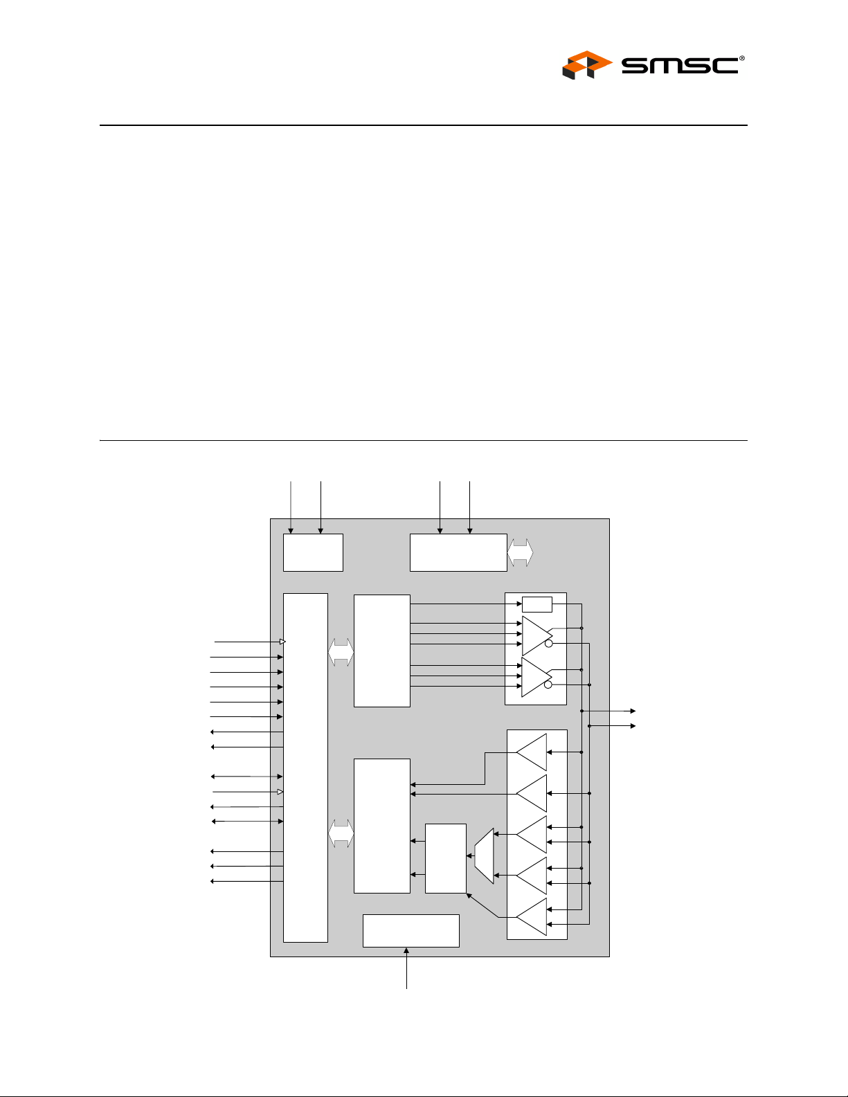
General Description
The USB3250 provides the Physical Layer (PHY) interface to a USB 2.0 Device Controller. The IC is
available in a 56 pin QFN.
The USB3250 is a USB 2.0 physical layer transceiver (PHY) integrated circuit. SMSC's proprietary
technology results in low power dissipation, which is ideal for building a bus powered USB 2.0
peripheral. The PHY can be configured for either an 8-bit unidirectional or a 16-bit bidirectional parallel
interface, which complies with the USB Transceiver Macrocell Interface (UTMI) specification. It
supports 480Mbps transfer rate, while remaining backward compatible with USB 1.1 legacy protocol
at 12Mbps.
All required termination for the USB 2.0 Transceiver is internal. Internal 5.25V short circuit protection
of DP and DM lines is provided for USB compliance.
While transmitting data, the PHY serializes data and generates SYNC and EOP fields. It also performs
needed bit stuffing and NRZI encoding. Likewise, while receiving data, the PHY de-serializes incoming
data, stripping SYNC and EOP fields and performs bit un-stuffing and NRZI decoding.
Block Diagram
DATABUS16_8
RESET
SUSPENDN
XCVRSELECT
TERMSELECT
O
P
M
O
D
E
[
:
1
LINESTATE[1:0]
CLKOUT
0
:
]
5
1
A
[
T
D
A
TXVALID
A
R
T
D
E
Y
X
A
L
V
D
I
H
X
R
I
L
D
V
A
C
I
A
V
T
X
E
R
R
X
E
R
O
R
R
VDD3.3
VDD1.8
PWR
CONTROL
TX
LOGIC
TX State
Machine
Parallel to
Serial
Conversion
Bit Stuff
NRZ
Encode
]
0
HS_DRIVE_ENABLE
RX
LOGIC
*
UTMI Interface
RX State
Machine
Serial to
Parallel
Conversion
Bit Unstuff
NRZI
Decode
Recovery Unit
Recovery
Elasticity
XO
XI
PLL and
XTAL OSC
RPU_EN
VPO
VMO
OEB
HS_DATA
HS_CS_ENABLE
VP
VM
Clock
Clock
and
Data
Buffer
MUX
1.5k
FS
TX
HS
TX
RX
SE+
SE-
RX
HS
RX
TX
FS
FS
FS
System
Clocking
Ω
DP
DM
BIASING
Bandgap Voltage Reference
Current Reference
RBIAS
HS
SQ
Figure 1 USB3250 Functional Block Diagram
SMSC USB3250 3 Revision 1.7 (05-11-07)
PRODUCT PREVIEW
Page 4

Pin Configuration
Hi-Speed USB Device Transceiver with UTMI Interface
VSSA
DM
DP
VDDA3.3
VSSA
RBIAS
VDDA3.3
VSSA
VSSA
XO
VDDA1.8
SUSPENDN
VSS
VDD1.8
DATABUS16_8
VSS
VSS
56555453525150
1
2
3
4
5
6
7
8
9
XI
10
11
12
13
14
15161718192021222324252627
VDD1.8
VDD3.3
RXERROR
USB 2.0
USB3250
PHY IC
OPMODE[1]
XCVRSELECT
TERMSELECT
CLKOUT
RXACTIVE
TXREADY
49
OPMODE[0]
LINESTATE[1]
VALIDH
VSS
RXVALID
4847464544
RESET
VDD1.8
DATA[15]
LINESTATE[0]
TXVALID
DATA[14]
Figure 2 56-Pin USB3250 Pin Configuration (Top View)
DATA[0]
DATA[13]
VDD3.3
43
42
41
40
39
38
37
36
35
34
33
32
31
30
29
28
VDD3.3
DATA[1]
DATA[2]
DATA[3]
DATA[4]
VDD1.8
DATA[5]
DATA[6]
DATA[7]
DATA[8]
VSS
DATA[9]
DATA[10]
DATA[11]
DATA[12]
Revision 1.7 (05-11-07) 4 SMSC USB3250
PRODUCT PREVIEW
Page 5

Hi-Speed USB Device Transceiver with UTMI Interface
Pin Description Tables
Table 1 System Interface Pins
ACTIVE
NAME DIRECTION
LEVEL DESCRIPTION
RESET Input High Reset. Reset all state machines. After coming out of reset, must
XCVRSELECT Input N/A Transceiver Select. This signal selects between the FS and HS
TERMSELECT Input N/A Termination Select. This signal selects between the FS and HS
SUSPENDN Input Low Suspend. Places the transceiver in a mode that draws minimal
CLKOUT Output Rising Edge System Clock. This output is used for clocking receive and
OPMODE[1:0] Input N/A Operational Mode. These signals select between the various
LINESTATE[1:0] Output N/A Line State. These signals reflect the current state of the USB
DATABUS16_8 Input N/A Databus Select. Selects between 8-bit and 16-bit data transfers.
wait 5 rising edges of clock before asserting TXValid for transmit.
Assertion of Reset: May be asynchronous to CLKOUT.
De-assertion of Reset: Must be synchronous to CLKOUT unless
RESET is asserted longer than two periods of CLKOUT.
transceivers:
0: HS transceiver enabled
1: FS transceiver enabled.
terminations:
0: HS termination enabled
1: FS termination enabled
power from supplies. Shuts down all blocks not necessary for
Suspend/Resume operation. While suspended, TERMSELECT
must always be in FS mode to ensure that the 1.5k Ω pull-up on
DP remains powered.
0: Transceiver circuitry drawing suspend current
1: Transceiver circuitry drawing normal current
transmit parallel data at 60MHz (8-bit mode) or 30MHz (16-bit
mode). When in 8-bit mode, this specification refers to CLKOUT
as CLK60. When in 16-bit mode, CLKOUT is referred to as
CLK30.
operational modes:
[1] [0] Description
0 0 0: Normal Operation
0 1 1: Non-driving (all terminations removed)
1 0 2: Disable bit stuffing and NRZI encoding
1 1 3: Reserved
data bus in FS mode, with [0] reflecting the state of DP and [1]
reflecting the state of DM. When the device is suspended or
resuming from a suspended state, the signals are combinatorial.
Otherwise, the signals are synchronized to CLKOUT.
[1] [0] Description
0 0 0: SE0
0 1 1: J State
1 0 2: K State
1 1 3: SE1
0: 8-bit data path enabled. VALIDH is undefined. CLKOUT =
60MHz.
1: 16-bit data path enabled. CLKOUT = 30MHz.
SMSC USB3250 5 Revision 1.7 (05-11-07)
PRODUCT PREVIEW
Page 6

ACTIVE
NAME DIRECTION
DATA[15:0] Bidir N/A
LEVEL DESCRIPTION
Hi-Speed USB Device Transceiver with UTMI Interface
Table 2 Data Interface Pins
DATA BUS. 16-BIT BIDIRECTIONAL MODE.
TXVALID RXVALID VALIDH DATA[15:0]
0 0 X Not used
0 1 0 DATA[7:0] output is valid
for receive
VALIDH is an output
0 1 1 DATA[15:0] output is
valid for receive
VALIDH is an output
1 X 0 DATA[7:0] input is valid
for transmit
VALIDH is an input
1 X 1 DATA[15:0] input is valid
for transmit
VALIDH is an input
DATA BUS. 8-BIT UNIDIRECTIONAL MODE.
TXVALID RXVALID DATA[15:0]
00Not used
0 1 DATA[15:8] output is valid for receive
1 X DATA[7:0] input is valid for transmit
TXVALID Input High Tra nsmi t Valid. Indicates that the TXDATA bus is valid for
TXREADY Output High Transmit Data Ready. If TXVALID is asserted, the SIE must
VAL IDH Bi dir N/ A Transmit/Receive High Data Bit Valid (used in 16-bit mode
RXVALID Output High Receive Data Valid. Indicates that the RXDATA bus has received
RXACTIVE Output High Receive Active. Indicates that the receive state machine has
RXERROR Output High Receive Error. 0: Indicates no error. 1: Indicates a receive error
transmit. The assertion of TXVALID initiates the transmission of
SYNC on the USB bus. The negation of TXVALID initiates EOP
on the USB.
Control inputs (OPMODE[1:0], TERMSELECT,XCVRSELECT)
must not be changed on the de-assertion or assertion of TXVALID.
The PHY must be in a quiescent state when these inputs are
changed.
always have data available for clocking into the TX Holding
Register on the rising edge of CLKOUT. TXREADY is an
acknowledgement to the SIE that the transceiver has clocked the
data from the bus and is ready for the next transfer on the bus. If
TXVALID is negated, TXREADY can be ignored by the SIE.
only). When TXVALID = 1, the 16-bit data bus direction is
changed to inputs, and VALIDH is an input. If VALIDH is asserted,
DATA[15:0] is valid for transmission. If deasserted, only DATA[7:0]
is valid for transmission. The DATA bus is driven by the SIE.
When TXVALID = 0 and RXVALID = 1, the 16-bit data bus
direction is changed to outputs, and VALIDH is an output. If
VALIDH is asserted, the DATA[15:0] outputs are valid for receive.
If deasserted, only DATA[7:0] is valid for receive. The DATA bus
is read by the SIE.
valid data. The Receive Data Holding Register is full and ready to
be unloaded. The SIE is expected to latch the RXDATA bus on the
rising edge of CLKOUT.
detected Start of Packet and is active.
has been detected. This output is clocked with the same timing as
the RXDATA lines and can occur at anytime during a transfer.
Revision 1.7 (05-11-07) 6 SMSC USB3250
PRODUCT PREVIEW
Page 7

Hi-Speed USB Device Transceiver with UTMI Interface
Table 3 USB I/O Pins
ACTIVE
NAME DIRECTION
DP I/O N/A USB Positive Data Pin.
DM I/O N/A USB Negative Data Pin.
LEVEL DESCRIPTION
Table 4 Biasing and Clock Oscillator Pins
NAME DIRECTION
RBIAS Input N/A External 1% bias resistor. Requires a 12KΩ resistor to ground.
XI/XO Input N/A External crystal. 12MHz crystal connected from XI to XO.
NAME DIRECTION
VDD3.3 N/A N/A 3.3V Digital Supply. Powers digital pads. See Note 2.1
VDD1.8 N/A N/A 1.8V Digital Supply. Powers digital core.
VSS N/A N/A Digital Ground. See Note 2.2
VDDA3.3 N/A N/A 3.3V Analog Supply. Powers analog I/O and 3.3V analog
VDDA1.8 N/A N/A 1.8V Analog Supply. Powers 1.8V analog circuitry. See Note 2.1
VSSA N/A N/A Analog Ground. See Note 2.2
Note 2.1 A Ferrite Bead (with DC resistance <.5 Ohms) is recommended for filtering between both
the VDD3.3 and VDDA3.3 supplies and the VDD1.8 and VDDA1.8 Supplies.
Note 2.2 All VSS and VSSA are bonded to the exposed pad under the IC in the package. The
exposed pad must be connected to solid GND plane on printed circuit board.
ACTIVE
LEVEL DESCRIPTION
Used for setting HS transmit current level and on-chip termination
impedance.
Table 5 Power and Ground Pins
ACTIVE
LEVEL DESCRIPTION
circuitry.
SMSC USB3250 7 Revision 1.7 (05-11-07)
PRODUCT PREVIEW
Page 8

Application Diagram
Hi-Speed USB Device Transceiver with UTMI Interface
1uF
VDD3.3
10uF
Voltage
Regulator
10uF
VDD1.8
10uF
1uF
C LOAD
12MHz
Crystal
C LOAD
Ferrite Bead
Ferrite Bead
1ΜΩ
VDD1.8
44
42
41
40
39
37
36
35
34
32
31
30
29
27
26
25
10
11
12
VDDA1.8
16
VDD1.8
23
VDD1.8
38
VDD1.8
53
VDD1.8
4
VDDA3.3
7
VDDA3.3
15
VDD3.3
28
VDD3.3
43
VDD3.3
DATA 0
DATA 1
DATA 2
DATA 3
DATA 4
DATA 5
DATA 6
DATA 7
DATA 8
DATA 9
DATA 10
DATA 11
DATA 12
DATA 13
DATA 14
DATA 15
XI
XO
UTMI
DATABUS16_8
XCVRSELECT
TERMSELECT
USB
POWER
TXVALID
TXREADY
RXACTIVE
RXVALID
RXERROR
VALIDH
SUSPENDN
RESET
OPMODE 0
OPMODE 1
LINESTATE 0
LINESTATE 1
CLKOUT
RBIAS
DP
DM
VSSA
VSSA
VSSA
VSSA
VSS
VSS
VSS
VSS
VSS
45
51
50
46
52
47
54
17
18
13
24
20
19
22
21
49
14
33
48
55
56
6
12KΩ
3
USB-B
2
1
5
8
9
VDD3.3
GND
Figure 3 Application Diagram for 56-pin QFN Package
Revision 1.7 (05-11-07) 8 SMSC USB3250
PRODUCT PREVIEW
Page 9

Revision 1.7 (05-11-07) 9 SMSC USB3250
Package Outline
3
TERMINAL #1
IDENTIFIER AREA
(D1/2 X E1/2)
4X 45°X0.6 MAX (OPTIONAL)
PRODUCT PREVIEW
D
D1
TOP VIEW
Hi-Speed USB Device Transceiver with UTMI Interface
REVISION HISTORY
D2
e
E2EE1
TERMINAL #1
IDENTIFIER AR EA
(D/2 X E/2)
EXPOSED PAD
3
2
A INITIAL R ELEASE 2/07/04 S.K.ILIEV
B REMO VE "PREL IMINARY" NOTE 10/7/04 S.K.ILIEV
L(MAX ) FROM 0 .55 TO 0.50. AD DED D2/E2 VARIATIONS TABLE
C
56X L
2
56X b
BOTTOM VIEW
DESCRIPTIONREVISION RELEASED BYDATE
7/2/05 S .K.ILIEV
A
A2
A1
SIDE VIEW
D2 / E2 VARIATIONS
CATALOG PART
NOTES:
1. A LL DIM ENSION S AR E IN M ILL IM ETER .
2. POSITION TOLERANCE OF EACH TERMINAL AND EXPOSED PAD IS ± 0.05mm AT MAXIMUM MATERIAL
CO NDITION. DIMENS IONS "b" APP LIES TO PLATED TER MINALS AND IT IS M EASURED BETWEEN 0.15 AND
0. 30 m m FRO M THE TER M INAL TIP.
3. DETAILS OF TERMINA L #1 IDENTIFIER A RE OPTION AL BUT M UST BE LOC ATED W ITHIN THE AREA INDICATED.
ANGULAR
±1°
THIRD ANGLE PROJECTION
NAME
DRAWN
S.K.ILIEV
CHECKED
S.K.ILIEV
APPROVED
S.K.ILIEV
80 ARKAY DRIVE
HAU PPA UG E, N Y 11788
USA
TITLE
DATE
2/06/04
2/07/04 C
2/07 /04 1 :1
56 TERMINAL QFN, 8x8mm BODY, 0.5mm PITCH
DWG NUMBER
SCALE
PACKAGE OUTLINE
MO-56-QFN-8x8
STD COMPLIANCE
JE DEC: MO -220 1 O F 1
REV
SHEET
3-D VIEWS
UNLE SS OTH ERW ISE SPECIFIED
DIMENSIONS ARE IN MILLIMETERS
AN D TOLERANCES ARE:
DECIMAL
±0.1
X.X
±0.05
X.XX
±0.025
X.XXX
DIM AN D TO L PE R AS ME Y14.5M - 1994
MATERIAL
FINISH
-
-
PRINT WITH "SCALE TO FIT"
DO NOT SCALE DRAWING
 Loading...