

Page 1

USB2524
PRODUCT FEATURES
USB 2 .0 Compatible 4-Port Hub with two upstream
host port connections
— Provides electronic reconfiguration and re-assignment
of any of its 4 downstream ports to either of two
upstream host ports (“on-the-fly”).
— Allows multiple USB hosts to share peripherals and
enables a user to dynamically assign host ownership.
– Embedded Mode - 8 (predefined, OEM
programmable) configurations for port
assignment are selectable via three external
control signals.
– Peripheral Mode - Dedicated select pin for
every downstream port (total of 4), selectable
edge or level triggered in order to support a
wide range of possible switch configurations
and styles.
— Each host has a dedicated Single Transaction
Translator (Single-TT) for supporting FS/LS devices, or
can also operate in Multi-TT mode where each
downstream port has a dedicated Transaction
Translator.
Do wnstream ports can be d isabled or d efine d as non-
removable
Swi tching hub can be configured as compound
device for support of ‘embedded’ USB peripherals
Multiple LED modes for maximum implementation
flexibility
— USB Mode - 2 Single-color LEDs for each downstream
port (total of 8 LEDs).
— Host Ownership Mode - 8 Single-Color LEDs indicate
which upstream host each of the downstream ports are
assigned to.
— Host Ownership & Port Speed Mode - 8 Dual-Color
LEDs are used to indicate which upstream host each of
the downstream ports are assigned to, while
simultaneously indicating downstream port connection
speed.
USB MultiSwitch
TM
Hub
Datasheet
En hanced configuration options available through
either a Single Serial I
2
C EEPROM, or SMBus Slave
Port
— VID/PID/DID
— Port Configuration
— String Descriptors (each can support a maximum length
of 31 characters)
– Custom Manufacturer String
– Custom Prod uct String
– Custom Seri al String
— Assignment of downstream ports to upstream hosts
— Switching mechanism selection
H ardware Strapping options allow for configuration
without an external EEPROM or SMBus Host
— Default VID/PID/DID, allows functionality when
configuration EEPROM is absent
C omplete USB Specification 2.0 Compatibility
— Includes USB 2.0 Hi-Speed Transceivers
— High-Speed (480Mbits/s), Full-Speed (12Mbits/s) and
Low-Speed (1.5Mbits/s) compatible
— Full power management with choice of Individual or
Ganged power control
On-Boa rd 24MHz Crystal Driver Circuit or 24 MHz
external clock driver
Interna l PLL for 480MHz USB 2.0 Sampling
Interna l 1.8V Linear Voltage Regulator
Integ rated USB termination and Pull-up/Pull-down
resistors
Interna l Short Circuit protection of USB differential
signal pins
1 .8 Volt Low Power Core Operation
3 .3 Volt I/O with 5V Input Tolerance
5 6-Pin QFN Lead-free RoHS Compliant Package
SMSC USB2524 DATASHEET Revision 1.91 (08-22-07)
Page 2

USB MultiSwitch
TM
Hub
Datasheet
ORDER NUMBER(S):
USB2524-ABZJ for 56-pin QFN Lead-Free RoHS Compliant Package
80 ARKAY DRIVE, HAUPPAUGE, NY 11788 (631) 435-6000, FAX (631) 273-3123
Copyright © 2007 SMSC or its subsidiaries. All rights reserved.
Circuit diagrams and other information relating to SMSC products are included as a mean s of illustrating typical applications. Conse quently, complete information sufficient for
construction purposes is not necessarily given. Although the information has been checked and is believed to be accurate, no responsibility is assumed for inaccuracies. SMSC
reserves the right to make changes to specifications and product descriptions at any time without notice. Contact your local SMSC sales office to obtain the latest specifications
before placing your product order. The provision of this information does not convey to the purchaser of the described semiconductor devices any licenses under any patent
rights or other intellectual property rights of SMSC or others. All sales are expressly conditional on your agreement to the terms and conditions of the most recently da ted
version of SMSC's standard Terms of Sale Agreement dated before the date of your order (the "Terms of Sale Agreement"). The product may contain design defects or errors
known as anomalies which may cause the product's functions to deviate from published specifications. Anomaly sheets are available upon request. SMSC products are not
designed, intended, authorized or warranted for use in any life support or other application where product failure could cause or contribute to personal injury or severe property
damage. Any and all such uses without prior written approval of an Officer of SMSC and further testing and/or modification will be fully at the risk of the customer. Copies of
this document or other SMSC literature, as well as the Terms of Sale Agreement, may be obtained by visiting SMSC’s website at http://www.smsc.com. SMSC is a registered
trademark of Standard Microsystems Corporation (“SMSC”). Product names and company names are the trademarks of their respective holders.
SMSC DISCLAIMS AND EXCLUDES ANY AND ALL WARRANTIES, INCLUDING WITHOUT LIMITATION ANY AND ALL IMPLIED WARRANTIES OF MERCHANTABILITY,
FITNESS FOR A PARTICULAR PURPOSE, TITLE, AND AGAINST INFRINGEMENT AND THE LIKE, AND ANY AND ALL WARRANTIES ARISING FROM ANY COURSE
OF DEALING OR USAGE OF TRADE. IN NO EVENT SHALL SMSC BE LIABLE FOR ANY DIRECT, INCIDENTAL, INDIRECT, SPECIAL, PUNITIVE, OR CONSEQUENTIAL
DAMAGES; OR FOR LOST DATA, PROFITS, SAVINGS OR REVENUES OF ANY KIND; REGARDLESS OF THE FORM OF ACTION, WHETHER BASED ON CONTRACT;
TORT; NEGLIGENCE OF SMSC OR OTHERS; STRICT LIABILITY; BREACH OF WARRANTY; OR OTHERWISE; WHETHER OR NOT ANY REMEDY OF BUYER IS HELD
TO HAVE FAILED OF ITS ESSENTIAL PURPOSE, AND WHETHER OR NOT SMSC HAS BEEN ADVISED OF THE POSSIBILITY OF SUCH DAMAGES.
Revision 1.91 (08-22-07) 2 SMSC USB2524
DATASHEET
Page 3

USB MultiSwitch
Datasheet
TM
Hub
Table of Contents
Chapter 1 General Description. . . . . . . . . . . . . . . . . . . . . . . . . . . . . . . . . . . . . . . . . . . . . . . . . 8
1.1 OEM Selectable Features. . . . . . . . . . . . . . . . . . . . . . . . . . . . . . . . . . . . . . . . . . . . . . . . . . . . . . . . . 9
Chapter 2 Pin Layout . . . . . . . . . . . . . . . . . . . . . . . . . . . . . . . . . . . . . . . . . . . . . . . . . . . . . . . 10
Chapter 3 Pin Configuration . . . . . . . . . . . . . . . . . . . . . . . . . . . . . . . . . . . . . . . . . . . . . . . . . 11
Chapter 4 Switching Hub Pin Descriptions. . . . . . . . . . . . . . . . . . . . . . . . . . . . . . . . . . . . . . 12
Chapter 5 Switching Hub Block Diagram. . . . . . . . . . . . . . . . . . . . . . . . . . . . . . . . . . . . . . . 17
Chapter 6 Assigning Ports. . . . . . . . . . . . . . . . . . . . . . . . . . . . . . . . . . . . . . . . . . . . . . . . . . . . 18
6.1 Port Assign Interface (PRT_ASSIGN[3:0] pins) . . . . . . . . . . . . . . . . . . . . . . . . . . . . . . . . . . . . . . . 18
6.1.1 Embedded Mode: . . . . . . . . . . . . . . . . . . . . . . . . . . . . . . . . . . . . . . . . . . . . . . . . . . . . . . 18
6.1.2 Peripheral Mode: Level Triggered . . . . . . . . . . . . . . . . . . . . . . . . . . . . . . . . . . . . . . . . . . 19
6.1.3 Peripheral Mode: Edge Triggered . . . . . . . . . . . . . . . . . . . . . . . . . . . . . . . . . . . . . . . . . . 19
6.2 SMBus Host Control of Port Assignment . . . . . . . . . . . . . . . . . . . . . . . . . . . . . . . . . . . . . . . . . . . . 19
Chapter 7 Configuration Options. . . . . . . . . . . . . . . . . . . . . . . . . . . . . . . . . . . . . . . . . . . . . . 20
7.1 Switching Hub Configuration Options. . . . . . . . . . . . . . . . . . . . . . . . . . . . . . . . . . . . . . . . . . . . . . . 20
7.1.1 Power Switching Polarity. . . . . . . . . . . . . . . . . . . . . . . . . . . . . . . . . . . . . . . . . . . . . . . . . 20
7.1.2 VBus Detect. . . . . . . . . . . . . . . . . . . . . . . . . . . . . . . . . . . . . . . . . . . . . . . . . . . . . . . . . . . 20
7.1.3 Port Assignment Configuration:. . . . . . . . . . . . . . . . . . . . . . . . . . . . . . . . . . . . . . . . . . . . 20
7.1.4 Internal Register Set (Common to EEPROM and SMBus) . . . . . . . . . . . . . . . . . . . . . . . 20
7.1.4.1 Register 00h: Vendor ID (LSB) (Reset = 0x00). . . . . . . . . . . . . . . . . . . . . . . . . . . . . . . . 22
7.1.4.2 Register 01h: Vendor ID (MSB) (Reset = 0x00) . . . . . . . . . . . . . . . . . . . . . . . . . . . . . . . 22
7.1.4.3 Register 02h: Product ID (LSB) (Reset = 0x00) . . . . . . . . . . . . . . . . . . . . . . . . . . . . . . . 22
7.1.4.4 Register 03h: Product ID (MSB) (Reset = 0x00) . . . . . . . . . . . . . . . . . . . . . . . . . . . . . . . 22
7.1.4.5 Register 04h: Device ID (LSB) (Reset = 0x00) . . . . . . . . . . . . . . . . . . . . . . . . . . . . . . . . 22
7.1.4.6 Register 05h: Device ID (MSB) (Reset = 0x00). . . . . . . . . . . . . . . . . . . . . . . . . . . . . . . . 22
7.1.4.7 Register 06h: CONFIG_BYTE_1 (Reset = 0x00) . . . . . . . . . . . . . . . . . . . . . . . . . . . . . . 23
7.1.4.8 Register 07h: Configuration Data Byte 2 (Reset = 0x00) . . . . . . . . . . . . . . . . . . . . . . . . 24
7.1.4.9 Register 08h: Configuration Data Byte 3 (Reset = 0x00) . . . . . . . . . . . . . . . . . . . . . . . . 24
7.1.4.10 Register 09h: Non-Removable Device (Reset = 0x00) . . . . . . . . . . . . . . . . . . . . . . . . . . 25
7.1.4.11 Register 0Ah: Port Disable For Self Powered Operation (Reset = 0x00) . . . . . . . . . . . . 26
7.1.4.12 Register 0Bh: Port Disable For Bus Powered Operation (Reset = 0x00) . . . . . . . . . . . . 26
7.1.4.13 Register 0Ch: Max Power For Self Powered Operation (Reset = 0x00) . . . . . . . . . . . . . 26
7.1.4.14 Register 0Dh: Max Power For Bus Powered Operation (Reset = 0x00) . . . . . . . . . . . . . 27
7.1.4.15 Register 0Eh: Hub Controller Max Current For Self Powered Operation (Reset = 0x00) 27
7.1.4.16 Register 0Fh: Hub Controller Max Current For Bus Powered Operation (Reset = 0x00) 27
7.1.4.17 Register 10h: Power-On Time (Reset = 0x00) . . . . . . . . . . . . . . . . . . . . . . . . . . . . . . . . 27
7.1.4.18 Register 11h: Language ID High (Reset = 0x00). . . . . . . . . . . . . . . . . . . . . . . . . . . . . . . 27
7.1.4.19 Register 12h: Language ID Low (Reset = 0x00) . . . . . . . . . . . . . . . . . . . . . . . . . . . . . . . 27
7.1.4.20 Register 13h: Manufacturer String Length (Reset = 0x00) . . . . . . . . . . . . . . . . . . . . . . . 28
7.1.4.21 Register 14h: Product String Length (Reset = 0x00). . . . . . . . . . . . . . . . . . . . . . . . . . . . 28
7.1.4.22 Register 15h: Serial String Length (Reset = 0x00) . . . . . . . . . . . . . . . . . . . . . . . . . . . . . 28
7.1.4.23 Register 16h-53h: Manufacturer String (Reset = 0x00). . . . . . . . . . . . . . . . . . . . . . . . . . 28
7.1.4.24 Register 54h-91h: Product String (Reset = 0x00) . . . . . . . . . . . . . . . . . . . . . . . . . . . . . . 28
7.1.4.25 Register 92h-CFh: Serial String (Reset = 0x00) . . . . . . . . . . . . . . . . . . . . . . . . . . . . . . . 29
7.1.4.26 Register D0h: Port Interface Delay Timer (Reset = 0x00) . . . . . . . . . . . . . . . . . . . . . . . 29
7.1.4.27 Register D1h: Port Assign Interface Configuration 0A (Reset = 0x00) . . . . . . . . . . . . . . 29
SMSC USB2524 3 Revision 1.91 (08-22-07)
DATASHEET
Page 4

USB MultiSwitch
TM
Hub
Datasheet
7.1.4.28 Register D2h: Port Assign Interface Configuration 0B (Reset = 0x00) . . . . . . . . . . . . . . 30
7.1.4.29 Register D3h: Port Assign Interface Configuration 0C (Reset = 0x00) . . . . . . . . . . . . . . 30
7.1.4.30 Register D4h: Port Assign Interface Configuration 0D (Reset = 0x00) . . . . . . . . . . . . . . 30
7.1.4.31 Register D5h: Port Assign Interface Configuration 1A (Reset = 0x00) . . . . . . . . . . . . . . 30
7.1.4.32 Register D6h: Port Assign Interface Configuration 1B (Reset = 0x00) . . . . . . . . . . . . . . 31
7.1.4.33 Register D7h: Port Assign Interface Configuration 1C (Reset = 0x00) . . . . . . . . . . . . . . 31
7.1.4.34 Register D8h: Port Assign Interface Configuration 1D (Reset = 0x00) . . . . . . . . . . . . . . 31
7.1.4.35 Register D9h: Port Assign Interface Configuration 2A (Reset = 0x00) . . . . . . . . . . . . . . 31
7.1.4.36 Register DAh: Port Assign Interface Configuration 2B (Reset = 0x00) . . . . . . . . . . . . . . 32
7.1.4.37 Register DBh: Port Assign Interface Configuration 2C (Reset = 0x00) . . . . . . . . . . . . . . 32
7.1.4.38 Register DCh: Port Assign Interface Configuration 2D (Reset = 0x00). . . . . . . . . . . . . . 32
7.1.4.39 Register DDh: Port Assign Interface Configuration 3A (Reset = 0x00) . . . . . . . . . . . . . . 32
7.1.4.40 Register DEh: Port Assign Interface Configuration 3B (Reset = 0x00) . . . . . . . . . . . . . . 33
7.1.4.41 Register DFh: Port Assign Interface Configuration 3C (Reset = 0x00) . . . . . . . . . . . . . . 33
7.1.4.42 Register E0h: Port Assign Interface Configuration 3D (Reset = 0x00) . . . . . . . . . . . . . . 33
7.1.4.43 Register E1h: Port Assign Interface Configuration 4A (Reset = 0x00) . . . . . . . . . . . . . . 33
7.1.4.44 Register E2h: Port Assign Interface Configuration 4B (Reset = 0x00) . . . . . . . . . . . . . . 34
7.1.4.45 Register E3h: Port Assign Interface Configuration 4C (Reset = 0x00) . . . . . . . . . . . . . . 34
7.1.4.46 Register E4h: Port Assign Interface Configuration 4D (Reset = 0x00) . . . . . . . . . . . . . . 34
7.1.4.47 Register E5h: Port Assign Interface Configuration 5A (Reset = 0x00) . . . . . . . . . . . . . . 34
7.1.4.48 Register E6h: Port Assign Interface Configuration 5B (Reset = 0x00) . . . . . . . . . . . . . . 35
7.1.4.49 Register E7h: Port Assign Interface Configuration 5C (Reset = 0x00) . . . . . . . . . . . . . . 35
7.1.4.50 Register E8h: Port Assign Interface Configuration 5D (Reset = 0x00) . . . . . . . . . . . . . . 35
7.1.4.51 Register E9h: Port Assign Interface Configuration 6A (Reset = 0x00) . . . . . . . . . . . . . . 35
7.1.4.52 Register EAh: Port Assign Interface Configuration 6B (Reset = 0x00) . . . . . . . . . . . . . . 36
7.1.4.53 Register EBh: Port Assign Interface Configuration 6C (Reset = 0x00) . . . . . . . . . . . . . . 36
7.1.4.54 Register ECh: Port Assign Interface Configuration 6D (Reset = 0x00) . . . . . . . . . . . . . . 36
7.1.4.55 Register EDh: Port Assign Interface Configuration 7A (Reset = 0x00) . . . . . . . . . . . . . . 36
7.1.4.56 Register EEh: Port Assign Interface Configuration 7B (Reset = 0x00) . . . . . . . . . . . . . . 37
7.1.4.57 Register EFh: Port Assign Interface Configuration 7C (Reset = 0x00) . . . . . . . . . . . . . . 37
7.1.4.58 Register F0h: Port Assign Interface Configuration 7D (Reset = 0x00) . . . . . . . . . . . . . . 37
7.1.4.59 Register F1h: Port Assignment 1 & 2 (Reset = 0x00) . . . . . . . . . . . . . . . . . . . . . . . . . . . 37
7.1.4.60 Register F2h: Port Assignment 3 & 4 (Reset = 0x00) . . . . . . . . . . . . . . . . . . . . . . . . . . . 38
7.1.4.61 Register F3h: Port Assignment 5 & 6 (Reset = 0x00) . . . . . . . . . . . . . . . . . . . . . . . . . . . 38
7.1.4.62 Register F4h: Port Assignment 7 (Reset = 0x00) . . . . . . . . . . . . . . . . . . . . . . . . . . . . . . 38
7.1.4.63 Register F5h: Port Lockout (Reset = 0x00). . . . . . . . . . . . . . . . . . . . . . . . . . . . . . . . . . . 38
7.1.4.64 Register FFh: Status/Command (Reset = 0x00) . . . . . . . . . . . . . . . . . . . . . . . . . . . . . . . 39
7.2 EEPROM Interface. . . . . . . . . . . . . . . . . . . . . . . . . . . . . . . . . . . . . . . . . . . . . . . . . . . . . . . . . . . . . 40
7.2.1 I2C Master. . . . . . . . . . . . . . . . . . . . . . . . . . . . . . . . . . . . . . . . . . . . . . . . . . . . . . . . . . . . 40
7.2.1.1 Implementation Characteristics . . . . . . . . . . . . . . . . . . . . . . . . . . . . . . . . . . . . . . . . . . . . 40
7.2.1.2 Pull-Up Resistor. . . . . . . . . . . . . . . . . . . . . . . . . . . . . . . . . . . . . . . . . . . . . . . . . . . . . . . . 40
7.2.1.3 I2C EEPROM Slave Address . . . . . . . . . . . . . . . . . . . . . . . . . . . . . . . . . . . . . . . . . . . . . 40
7.2.2 In-Circuit EEPROM Programming. . . . . . . . . . . . . . . . . . . . . . . . . . . . . . . . . . . . . . . . . . 40
7.3 SMBus Slave Interface . . . . . . . . . . . . . . . . . . . . . . . . . . . . . . . . . . . . . . . . . . . . . . . . . . . . . . . . . . 41
7.3.1 Bus Protocols . . . . . . . . . . . . . . . . . . . . . . . . . . . . . . . . . . . . . . . . . . . . . . . . . . . . . . . . . 41
7.3.1.1 Block Read/Write. . . . . . . . . . . . . . . . . . . . . . . . . . . . . . . . . . . . . . . . . . . . . . . . . . . . . . . 41
7.3.2 Invalid Protocol Response Behavior . . . . . . . . . . . . . . . . . . . . . . . . . . . . . . . . . . . . . . . . 42
7.3.3 General Call Address Response . . . . . . . . . . . . . . . . . . . . . . . . . . . . . . . . . . . . . . . . . . . 42
7.3.4 Slave Device Time-Out . . . . . . . . . . . . . . . . . . . . . . . . . . . . . . . . . . . . . . . . . . . . . . . . . . 42
7.3.5 Stretching the SCLK Signal. . . . . . . . . . . . . . . . . . . . . . . . . . . . . . . . . . . . . . . . . . . . . . . 42
7.3.6 SMBus Timing . . . . . . . . . . . . . . . . . . . . . . . . . . . . . . . . . . . . . . . . . . . . . . . . . . . . . . . . . 42
7.3.7 Bus Reset Sequence. . . . . . . . . . . . . . . . . . . . . . . . . . . . . . . . . . . . . . . . . . . . . . . . . . . . 43
7.3.8 SMBus Alert Response Address. . . . . . . . . . . . . . . . . . . . . . . . . . . . . . . . . . . . . . . . . . . 43
7.3.8.1 Undefined Registers . . . . . . . . . . . . . . . . . . . . . . . . . . . . . . . . . . . . . . . . . . . . . . . . . . . . 43
7.3.8.2 Reserved Registers. . . . . . . . . . . . . . . . . . . . . . . . . . . . . . . . . . . . . . . . . . . . . . . . . . . . . 43
Revision 1.91 (08-22-07) 4 SMSC USB2524
DATASHEET
Page 5

USB MultiSwitch
Datasheet
7.4 Default Strapping Option . . . . . . . . . . . . . . . . . . . . . . . . . . . . . . . . . . . . . . . . . . . . . . . . . . . . . . . . 43
7.5 Default Configuration . . . . . . . . . . . . . . . . . . . . . . . . . . . . . . . . . . . . . . . . . . . . . . . . . . . . . . . . . . . 43
TM
Hub
Chapter 8 LED Interface Description . . . . . . . . . . . . . . . . . . . . . . . . . . . . . . . . . . . . . . . . . . 44
8.1 USB Mode: . . . . . . . . . . . . . . . . . . . . . . . . . . . . . . . . . . . . . . . . . . . . . . . . . . . . . . . . . . . . . . . . . . . 44
8.2 Basic Host Owner LED Indication: . . . . . . . . . . . . . . . . . . . . . . . . . . . . . . . . . . . . . . . . . . . . . . . . . 44
8.3 Host Ownership and Port Speed LED Indication:. . . . . . . . . . . . . . . . . . . . . . . . . . . . . . . . . . . . . . 45
Chapter 9 Reset . . . . . . . . . . . . . . . . . . . . . . . . . . . . . . . . . . . . . . . . . . . . . . . . . . . . . . . . . . . . 47
9.1 Reset . . . . . . . . . . . . . . . . . . . . . . . . . . . . . . . . . . . . . . . . . . . . . . . . . . . . . . . . . . . . . . . . . . . . . . . 47
9.1.1 External Hardware RESET_N . . . . . . . . . . . . . . . . . . . . . . . . . . . . . . . . . . . . . . . . . . . . . 47
9.1.1.1 RESET_N for Strapping Option Configuration. . . . . . . . . . . . . . . . . . . . . . . . . . . . . . . . . 48
9.1.1.2 RESET_N for EEPROM Configuration . . . . . . . . . . . . . . . . . . . . . . . . . . . . . . . . . . . . . . 49
9.1.1.3 RESET_N for SMBus Slave Configuration . . . . . . . . . . . . . . . . . . . . . . . . . . . . . . . . . . . 50
9.1.2 USB Bus Reset . . . . . . . . . . . . . . . . . . . . . . . . . . . . . . . . . . . . . . . . . . . . . . . . . . . . . . . . 50
Chapter 10 XNOR Test . . . . . . . . . . . . . . . . . . . . . . . . . . . . . . . . . . . . . . . . . . . . . . . . . . . . . . . 52
Chapter 11 DC Parameters. . . . . . . . . . . . . . . . . . . . . . . . . . . . . . . . . . . . . . . . . . . . . . . . . . . . 53
11.1 Maximum Guaranteed Ratings. . . . . . . . . . . . . . . . . . . . . . . . . . . . . . . . . . . . . . . . . . . . . . . . . . . . 53
11.1.1 DC Electrical Characteristics. . . . . . . . . . . . . . . . . . . . . . . . . . . . . . . . . . . . . . . . . . . . . . 53
Chapter 12 AC Specifications. . . . . . . . . . . . . . . . . . . . . . . . . . . . . . . . . . . . . . . . . . . . . . . . . . 56
12.1 Oscillator/Clock. . . . . . . . . . . . . . . . . . . . . . . . . . . . . . . . . . . . . . . . . . . . . . . . . . . . . . . . . . . . . . . . 56
12.1.1 SMBus Interface:. . . . . . . . . . . . . . . . . . . . . . . . . . . . . . . . . . . . . . . . . . . . . . . . . . . . . . . 56
12.1.2 I2C EEPROM: . . . . . . . . . . . . . . . . . . . . . . . . . . . . . . . . . . . . . . . . . . . . . . . . . . . . . . . . . 56
12.1.3 USB 2.0 . . . . . . . . . . . . . . . . . . . . . . . . . . . . . . . . . . . . . . . . . . . . . . . . . . . . . . . . . . . . . . 56
Chapter 13 Package Outline . . . . . . . . . . . . . . . . . . . . . . . . . . . . . . . . . . . . . . . . . . . . . . . . . . . 57
SMSC USB2524 5 Revision 1.91 (08-22-07)
DATASHEET
Page 6

USB MultiSwitch
TM
Hub
Datasheet
List of Figures
Figure 3.1 USB2524 QFN-56 . . . . . . . . . . . . . . . . . . . . . . . . . . . . . . . . . . . . . . . . . . . . . . . . . . . . . . . . . 11
Figure 5.1 USB2524 Switching Hub Block Diagram . . . . . . . . . . . . . . . . . . . . . . . . . . . . . . . . . . . . . . . . 17
Figure 7.1 SMBus Block Write . . . . . . . . . . . . . . . . . . . . . . . . . . . . . . . . . . . . . . . . . . . . . . . . . . . . . . . . 41
Figure 7.2 SMBus Block Read . . . . . . . . . . . . . . . . . . . . . . . . . . . . . . . . . . . . . . . . . . . . . . . . . . . . . . . . 42
Figure 7.3 LED Strapping Option . . . . . . . . . . . . . . . . . . . . . . . . . . . . . . . . . . . . . . . . . . . . . . . . . . . . . . 43
Figure 8.1 Dual Color LED Implementation Example . . . . . . . . . . . . . . . . . . . . . . . . . . . . . . . . . . . . . . . 45
Figure 9.1 Reset_N Timing for Default/Strap Option Mode. . . . . . . . . . . . . . . . . . . . . . . . . . . . . . . . . . . 48
Figure 9.2 Reset_N Timing for EEPROM Mode . . . . . . . . . . . . . . . . . . . . . . . . . . . . . . . . . . . . . . . . . . . 49
Figure 9.3 Reset_N Timing for SMBus Mode . . . . . . . . . . . . . . . . . . . . . . . . . . . . . . . . . . . . . . . . . . . . . 50
Figure 1 3. 1 USB2524 56-Pin QFN Package Outline and Paramete r s . . . . . . . . . . . . . . . . . . . . . . . . . . . 57
Revision 1.91 (08-22-07) 6 SMSC USB2524
DATASHEET
Page 7

USB MultiSwitch
Datasheet
TM
Hub
List of Tables
Table 2.1 USB2524 56-Pin QFN Pin Configuration Table. . . . . . . . . . . . . . . . . . . . . . . . . . . . . . . . . . . . 10
Table 4.1 Switching Hub Pin Descriptions. . . . . . . . . . . . . . . . . . . . . . . . . . . . . . . . . . . . . . . . . . . . . . . . 12
Table 4.2 SMBus or EEPROM Interface Behavior . . . . . . . . . . . . . . . . . . . . . . . . . . . . . . . . . . . . . . . . . 14
Table 4.3 Miscellaneous Pins . . . . . . . . . . . . . . . . . . . . . . . . . . . . . . . . . . . . . . . . . . . . . . . . . . . . . . . . . 15
Table 4.4 Power, Ground, and No Connect. . . . . . . . . . . . . . . . . . . . . . . . . . . . . . . . . . . . . . . . . . . . . . . 15
Table 4.5 Buffer Type Descriptions . . . . . . . . . . . . . . . . . . . . . . . . . . . . . . . . . . . . . . . . . . . . . . . . . . . . . 16
Table 6.1 USB2524 Port Assign Interface (Embedded Mode) . . . . . . . . . . . . . . . . . . . . . . . . . . . . . . . . 18
Table 7.1 Internal EEPROM & SMBus Register Memory Map . . . . . . . . . . . . . . . . . . . . . . . . . . . . . . . . 20
Table 9.1 Reset_N Timing for Default/Strap Option Mode . . . . . . . . . . . . . . . . . . . . . . . . . . . . . . . . . . . 48
Table 9.2 Reset_N Timing for EEPROM Mode . . . . . . . . . . . . . . . . . . . . . . . . . . . . . . . . . . . . . . . . . . . . 49
Table 9.3 Reset_N Timing for SMBus Mode . . . . . . . . . . . . . . . . . . . . . . . . . . . . . . . . . . . . . . . . . . . . . . 50
Table 11.1 DC Electrical Characteristics. . . . . . . . . . . . . . . . . . . . . . . . . . . . . . . . . . . . . . . . . . . . . . . . . . 53
SMSC USB2524 7 Revision 1.91 (08-22-07)
DATASHEET
Page 8

Chapter 1 General Description
The SMSC 4-Port USB 2.0 Switching Hub Controller acts as two independently controllable USB 2.0
Hubs in a single package with the ability to electronically reassign and reconfigure any of its 4
downstream ports to either of its two upstream USB ports. This allows two USB hosts to share
peripherals and to dynamically reconfigure them.
Any configuration of the downstream ports is possible except simultaneous connection to both
upstream ports. Up to 8 different configurations can be selected by a dedicated 3-pin interface, or the
4-pin interface can be used to directly assign each port to either of the upstream hosts. An external
serial EEPROM (or SMBus Host) is used to store the 8 different configuration parameters. However,
8 predefined configurations, as well as generic VID/PID/DID information, are provided as defaults if no
external Serial EEPROM is detected at power up. The SMBus interface can be used to configure the
hub as well as dynamically re-assigning downstream ports to upstream hosts. The SMBus interface
can be “live” while the hub is operational, and allows an external SMBus host to have full access to
re-assign ports on an as-needed basis.
The SMSC 4-Port Switching Hub is fully compliant with the USB 2.0 Specification and will attach to
either or both upstream USB hosts as a Full-Speed Hub or as a Full-/High-Speed Hub. The 4
downstream Hub ports support Low-Speed, Full-Speed, and High-Speed (if operating as a High-Speed
Hub) downstream devices on all of the enabled downstream ports.
USB MultiSwitch
Datasheet
TM
Hub
A USB peripheral or USB Hub that is attached to one of the downstream USB2524 ports will be
available to one or the other of the upstream USB host controllers, but can never be simultaneously
shared with both host controllers. The user can switch a peripheral from one host to the other (on-thefly), and the peripheral will automatically detach from one host and a ttach to the other host. Each host
will only configure and control the downstream ports that are assigned to it, including full USB power
management and suspend/resume operations.
The USB2524 works with an external USB power distribution switch device to con trol V
to downstream ports, and to limit current and sense over-current conditions.
All required resistors on the USB ports are integrated into the Hub. This includes all seri es termination
resistors on D+ and D– pins and all require d pull-down and pull-up resistors on D+ and D– pins. The
over-current sense inputs for the downstream facing ports have internal pull-up resistors.
Throughout this document the upstream facing port of the hub will be referred to as the upstream port,
and the downstream facing ports will be called the downstream ports.
For performance reasons, the Hub provides 1 Transaction Translator (TT) per port (defined as MultiTT configuration), and each TT has 1512 bytes of periodic buffer space and 272 Bytes of non- periodic
buffer space (divided into 4 non-periodic buffers per TT), for a total of 1784 bytes of buffer space for
each Transaction Translator.
When configured as a Single-TT Hub (required by USB 2.0 Specification), the Single Transaction
Translator will have 1512 bytes of periodic buffer space and 272 bytes of non-periodic buffer space
(divided into 4 non-periodic buffers per TT), for a total of 1784 bytes of buffer space for the entire
Transaction Translator.
switching
BUS
Revision 1.91 (08-22-07) 8 SMSC USB2524
DATASHEET
Page 9

USB MultiSwitch
Datasheet
TM
Hub
1.1 OEM Selectable Features
A default configuration is available in the USB2524 following a reset. This configuration may be
sufficient for some applications. Strapping option pins make it possible to modify a limited sub-set of
the configuration options.
The USB2524 may also be configured by an external EEPROM or a microcontroller. When using the
microcontroller interface, the Hub appears as an SMBus slave device. If the Hub is pin-strapped for
external EEPROM configuration but no external EEPROM is present, then a value of ‘0’ will be written
to all configuration data bit fields (the hub will attach to the ho st with all ‘0’ values).
The USB2524 supports several OEM selectable features:
Optional OEM configuration via I2C EEPROM or via the industry standard SMBus interface from
an external SMBus Host or Microcontroller.
Compound device support (port is permanently hardwired to a down strea m USB perip heral device).
Hardware strapping options enable configuration of the followin g features (when not configu red via
an EEPROM or SMBus host).
Non-Removable Ports
Port Power Polarity (active high or active low logic)
Selection of Single (STT) or Multi-Transaction Translator (MTT) capability.
Selection of Over-Current sensing a nd Port power control on a individual (port-b y-port) or ganged
(all ports together) to match the OEM’s choice of circuit board component selection.
Selection of end-user method of switching ports between hosts
-Embedded Mode: 8 default configurations that are controlled by OEM programmable registers (or
Internal default settings).
-Peripheral Mode: Each wire directly controls one of the 4 downstream ports. The interface is
selectable between edge triggered operation or level triggered operation for compatibility with many
different mechanical switch configurations or direct control from an external Microcontroller ’s GPIO
pins.
Enablement of String Descriptor Support, along with the capability to customize each of the 3
different string descriptors (up to a maximum size of 31 characters each)
Selection of LED Mode: USB Mode, Host Ownership Mode, or Host Ownersh ip Mode with Speed
Indication.
SMSC USB2524 9 Revision 1.91 (08-22-07)
DATASHEET
Page 10
USB MultiSwitch
Chapter 2 Pin Layout
T able 2.1 USB2524 56-Pin QFN Pin Configuration Table
UPSTREAM USB 2.0 INTERFACES (6 PINS)
USBUP_DP1 USBUP_DM1 USBUP_DP2 USBUP_DM2
VBUS_DET1 VBUS_DET2
DOWNSTREAM 4-PORT USB 2.0 INTERFACE (30 PINS)
USBDN_DP1 USBDN_DM1 USBDN_DP2 OCS1_N
USBDN_DP3 USBDN_DM3 USBDN_DM2 OCS2_N
LED_A1_N/NON_REM0 LED_A2_N/NON_REM1 LED_A3_N/PRT_DIS0 OCS3_N
LED_B1_N LED_B2_N LED_B3_N PRT_ASSIGN0
PRTPWR1 PRTPWR2 PRT_ASSIGN1 PRTPWR_POL
TM
Hub
Datasheet
PRTPWR3 RBIAS PRT_ASSIGN2 LED_A4_N/PRT_DIS1
USBDN_DM4 USBDN_DP4 PRTPWR4 PRT_ASSIGN3
LED_B4_N OCS4_N
SERIAL PORT INTERFACE (4 PINS)
SDA/SMBDATA SCL/SMBCLK/
CFG_SEL0
MISC (5 PINS)
XTAL1/CLKIN XTAL2 RESET_N SELF_PWR
TEST
ANALOG POWER & GROUND (5 PINS)
VDDPLL18(1)
DIGITAL POWER, GROUND & NO CONNECT (6 PINS)
VDD33(3) VDDCR18(2) NC
VDDA33(4)
TOTAL (56 PINS)
CFG_SEL1 CFG_SEL2
Revision 1.91 (08-22-07) 10 SMSC USB2524
DATASHEET
Page 11
USB MultiSwitch
Datasheet
TM
Hub
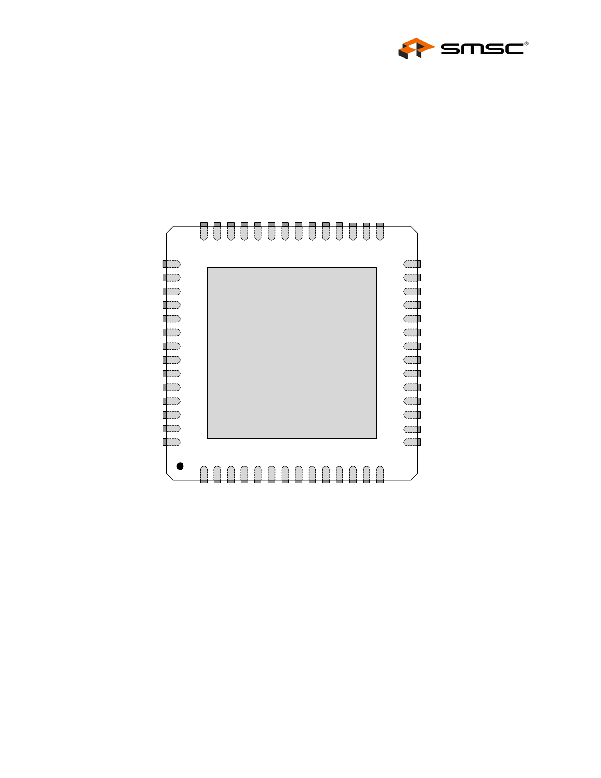
Chapter 3 Pin Configuration
41 PRT_ASSIGN0
40 PRT_ASSIGN1
39 PRT_ASSIGN2
38 PRT_ASSIGN3
37 VDD33
36 SELF_PWR
SMSC
LED_B4_N 43
RESET_N 44
VBUS_DET1 45
VBUS_DET2 46
VDDA33 47
USBUP_DP2 48
USBUP_DM2 49
VDDCR18 50
XTAL2 51
XTAL1/CLKIN 52
VDDPLL18 53
VDD33 54
NC 55
RBIAS 56
42 LED_A4_N/PRT_DIS1
USB2524
(Top View QFN-56)
thermal slug connects to VSS
35 CFG_SEL2
34 CFG_SEL1
32 SDA/SMBDATA
31 LED_B1_N
29 LED_B2_N
33 SCL /S MBCLK/CFG_SEL0
30 LED_A 1_N/NON_REM0
28 LED_A2_N/NON_REM1
27 PRTPWR1
26 OCS1_N
25 OCS2_N
24 PRTPWR2
23 PRTPWR3
22 OCS3_N
21 OCS4_N
20 PRTPWR4
19 PRTPWR_POL
18 TEST
17 VDD33
16 VDDCR18
15 LED_B3_N
VDDA33 1
USBUP_DP1 2
USBUP_DM1 3
VDDA33 6
USBDN_DP1 5
USBDN_DM1 4
USBDN_DP2 7
USBDN_DM2 8
VDDA33 11
USBDN_DP3 10
USBDN_DM3 9
USBDN_DP4 12
USBDN_DM4 13
LED_A3_N/PRT_DIS0 14
Figure 3.1 USB2524 QFN-56
SMSC USB2524 11 Revision 1.91 (08-22-07)
DATASHEET
Page 12
Chapter 4 Switching Hub Pin Descriptions
Table 4.1 Switching Hub Pin Descriptions
NAME SYMBOL TYPE FUNCTION
UPSTREAM USB 2.0 INTERFACE
USB MultiSwitch
Datasheet
TM
Hub
USB Bus Data USBUP_DP[2:1]
Detect Upstream
VBUS Power
High-Speed USB
Data
USB Power
Enable
Port 4:3 Green
LED
&
Port Disable
strapping option 0
USBUP_DM[2:1]
VBUS_DET[2:1] I/O Detects state of Upstream VBUS power. The SMSC Hub
USBDN_DP[4:1]
USBDN_DM[4:1]
PRTPWR[4:1] O Enables power to U SB peripheral devices (downstream).
LED_A[4:3]_N/
PRT_DIS[1:0]
IO-U These pins connect to the upstream USB bus data signals.
monitors VBUS_DET to determine when to assert the
internal D+ pull-up resistor (signalling a connect event).
When designing a detachable hub, this pin must be
connected to the VBUS power pin of the USB port that is
upstream of the hub. (Use of a weak pull-down resistor is
recommended.)
For self-powered applications with a permanently attached
host, this pin must be pulled-up to either 3.3V or 5.0V
(typically VDD33).
4-PORT USB 2.0 HUB INTERFACE
IO-U These pins connect to the downstream USB peripheral
devices attached to the Hub’s ports.
The active signal level of the PRTPWR[4] pin is determined
by the Power Polarity Strapping function of the
PRTPWR_POL pin.
I/O12 Green indicato r LED for ports 4 and 3. Will be active low
when LED support is enabled via EEPROM or SMBus. See
PRT_DIS1 function description if the hub is configured by
the internal default configuration.
Port Disable
strapping option 1
Revision 1.91 (08-22-07) 12 SMSC USB2524
PRT_DIS1 I/O12 If the hub is co nfigured by th e interna l default configuration ,
PRT_DIS[1:0] will be sampled at RESET_N negation to
determine if ports [4:2] will be permanently disabled. Also,
the active state of LED_A3_N will be determined as follows:
PRT_DIS[1:0] = '00', All ports are enabled,
LED_A4_N is active high,
LED_A3_N is active high.
PRT_DIS[1:0] = '01', Port 4 is disabled,
LED_A4_N is active high,
LED_A3_N is active low.
PRT_DIS[1:0] = '10', Ports 4 & 3 are disabled,
LED_A4_N is active low,
LED_A3_N is active high.
PRT_DIS[1:0] = '11', Ports 4, 3 & 2 are disabled,
LED_A4_N is active low,
LED_A3_N is active low.
DATASHEET
Page 13

USB MultiSwitch
Datasheet
TM
Hub
Table 4.1 Switching Hub Pin Descriptions (continued)
NAME SYMBOL TYPE FUNCTION
Port [2:1] Green
LED
&
Port Non-
Removable
strapping option
Enhanced Port
LED Indicators
LED_A[2:1]_N/
NON_REM[1:0]
I/O12 Green indicato r LED for ports 2 and 1. Will be active low
when LED support is enabled via EEPROM or SMBus.
If the hub is configured by the internal default configuration,
these pins will be sampled at RESET_N negation to
determine if ports [3:1] contain permanently attached (nonremovable) devices. Also, the active state of the LED's will
be determined as follows:
NON_REM[1:0] = '00', All ports are removable,
LED_A2_N is active high,
LED_A1_N is active high.
NON_REM[1:0] = '01', Port 1 is non-removable,
LED_A2_N is active high,
LED_A1_N is active low.
NON_REM[1:0] = '10', Ports 1 & 2 are non-removable,
LED_A2_N is active low,
LED_A1_N is active high.
NON_REM[1:0] = '11', Ports 1, 2, & 3 are non-removable,
LED_A2_N is active low,
LED_A1_N is active low.
LED_B[4:1]_N I/O12 T hese 4 pins in conjunction with the LED_A[4:1]_N pins
provides a total of 8 LED pins which are used to indicate
upstream host ownership of the downstream ports.
2 operational modes are available
Single Color LED Mode: LED will light to show which host
owns each of the downstream ports. If a port is
“unassigned” then neither LED for that port will light up.
Port Power
Polarity strapping
Over Current
Sense
USB Transceiver
Bias
Dual Color LED’s: (note; 4 possible states are displayed to
the user, Green, Red, Orange and Off).
PRTPWR_POL I/O Port Power Polarity strapping determination for the active
signal polarity of the PRTPWR[4:1] pins.
While RESET_N is asserted, the logic state of this pin will
(through the use of internal combinatorial logic) dete rmine
the active state of the PRTPWR[4:1] pins in order to ensure
that downstream port power is not inadvertently enabled to
inactive ports during a hardware reset.
When RESET_N is negated, the logic value will be latched
internally, and will retain the active signal polarity for the
PRTPWR[4:1] pins.
‘1’ = PRTPWR[4:1] pins have active ‘high’ polarity
‘0’ = PRTPWR[4:1] pins have active ‘low’ polarity
Warning: Active Low port power controllers may glitch
the downstream port power when system power is first
applied. Care should be taken when designing with
active low components!
OCS[4:1]_N IPU Input from external current monitor indicating an over-
current condition. {Note: Contains internal pull-up to 3.3V
supply}
RBIAS I-R A 12.0kΩ (+/− 1%) resistor is attached from ground to this
pin to set the transceiver’s internal bias settings.
SMSC USB2524 13 Revision 1.91 (08-22-07)
DATASHEET
Page 14
USB MultiSwitch
TM
Hub
Datasheet
Table 4.1 Switching Hub Pin Descriptions (continued)
NAME SYMBOL TYPE FUNCTION
Assign
Downstream
Ports to Upstream
Host Ports
Serial Data/SMB
Data
Serial Clock/SMB
Clock
&
Configuration
Programming
Select
Configuration
Programming
Select
Configuration
Programming
Select
PRT_ASSIGN
[3:0]
I Port Assign Interface: Operates in either Embedded mode,
or Peripheral mode. See Chapter 6, Assigning Ports for
additional details.
SERIAL PORT INTERFACE
SDA/SMBDATA IOSD12 (Serial Data)/(SMB Data) signal.
SCL/SMBCLK/
IOSD12 (Serial Clock)/(SMB Clock) signal.
CFG_SEL0
CFG_SEL0: The logic state of this multifunction pin is
internally latched on the rising edge of RESET_N
(RESET_N negation), and will determine the hub
configuration method as described in Table 4.2.
CFG_SEL1 I The logic state of this pin is internally latched on the rising
edge of RESET_N (RESET_N negation), and will determine
the hub configuration method as described in Table 4.2.
CFG_SEL2 I The logic state of this pin is internally latched on the rising
edge of RESET_N (RESET_N negation), and will determine
the hub configuration method as described in Table 4.2.
Table 4.2 SMBus or EEPROM Interface Behavior
NAME NAME NAME FUNCTION
CFG_SEL2 CFG_SEL1 CFG_SEL0 SMBus or EEPROM interface behavior.
0 0 0 Internal Default Configuration
PRT_ASSIGN[3:0] = Embedded Mode.
Strap options on pins LED_A[4:1]_N are enabled.
LED Mode = USB Mode
0 0 1 Configured as an SMBus slave for external download of
user-defined descriptors.
SMBus slave address is :0101100
Strap options on pins LED_A[4:1]_N are disabled
LED Mode = See C hapter 8, LED Interface Description
0 1 0 Internal Default Configuration
PRT_ASSIGN[3:0] = Peripheral Mode (Level Triggered)
Strap options on pins LED_A[4:1]_N are enabled.
No support for un assigned Ports.
LED Mode = USB Mode
0 1 1 2-wire (I2C) EEPROMS are supported,
LED Mode = See C hapter 8, LED Interface Description
Revision 1.91 (08-22-07) 14 SMSC USB2524
DATASHEET
Page 15
USB MultiSwitch
Datasheet
TM
Hub
Table 4.2 SMBus or EEPROM Interface Behavior (continued)
NAME NAME NAME FUNCTION
1 0 0 Internal Default Configuration
PRT_ASSIGN[3:0] = Peripheral Mode (Edge Triggered)
LED Mode = Host Ownershi p Mode
Strap
options on pins LED_A[4:1]_N are enabled.
Supports unassigned Ports
1 0 1 Internal Default Configuration
PRT_ASSIGN[3:0] = Peripheral Mode (Edge Triggered)
LED Mode = Host Ownershi p & Port Speed Mode
Strap options on pins LED_A[4:1]_N are disabled
Supports unassigned Ports.
110Reserved
111Reserved
Table 4.3 Miscellaneous Pins
NAME SYMBOL TYPE FUNCTION
Crystal
Input/External
Clock Input
XTAL1/
CLKIN
ICLKx
24MHz crystal or external clock input.
This pin connects to either one terminal of the crystal or
to an external 24MHz clock when a crystal is not used.
Note: See Table 11.1 for the required logic voltage
levels of this pad if it will be driven by an
external clock source.
Crystal Output XTAL2 OCLKx
24MHz Crystal
This is the other terminal of the crystal, or left
unconnected when an external clock source is used to
drive XTAL1/CLKIN. It must not be used to drive any
external circuitry other than the crystal circuit.
RESET Input RESET_N IS This active low signal is used by the system to reset the
chip. The minimum active low pulse is 1us.
Self-Power /
Bus-Power
Detect
SELF_PWR I Detects availability of local self-power source.
Low = Self/local power source is NOT available (i.e., Hub
gets all power from Upstream USB VBus).
High = Self/local power source is available.
TEST Pin TEST IPD Used for testing th e chip. User must treat as a no-
connect or connect to ground.
Table 4.4 Power, Ground, and No Connect
NAME SYMBOL TYPE FUNCTION
VDD Core VDDCR18 +1.8V core power.
Pins 16 and 50 must have a 4.7μF (or greater) ±20%
(ESR <0.1Ω) capacitor to VSS
VDDIO 3.3V VDD33 +3.3V Power Supply for the Digital I/O.
SMSC USB2524 15 Revision 1.91 (08-22-07)
DATASHEET
Page 16
Ta b le 4.4 Power, Ground, and No Connect (continued)
NAME SYMBOL TYPE FUNCTION
VDD PLL VDDPLL18 +1.8V Filtered analog power for internal PLL.
This pin must have a 4.7μF (or greater) ±20% (ESR
<0.1Ω) capacitor to VSS
USB MultiSwitch
Datasheet
TM
Hub
VDD Analog
I/O
VDDA33 +3.3V Filtered analog PHY power, shared between
adjacent ports.
VSS VSS Ground
NC NC No Connect
Table 4.5 Buffer Type Descriptions
BUFFER DESCRIPTION
I Input.
IPD Input, Weak Internal pull-down.
IPU Input, Weak Internal pull-up.
IS Input with Schmitt trigger.
IOSD12 Open drain….12mA sink with Schmitt trigger, and must meet I2C-Bus Specification Version 2.1
requirements.
ICLKx XTAL Clock Input
OCLKx XTAL Clock Output
I-R RBIAS
IO-U Defined in USB Specification.
Note: Meets USB 1.1 requirements when operating as a 1.1-complia nt device and meets
USB 2.0 requirements when operating as a 2.0-compliant device.
AIO Analog Input/output. Per PHY test require ments.
Revision 1.91 (08-22-07) 16 SMSC USB2524
DATASHEET
Page 17
Chapter 5 Switching Hub Block Diagram
To
Upstream
USB Data
Upstream
PHY
Repeater
Dow nstream
PHY #1
EEPROM
1.8V
Cap
TT#1TT#2TT#3TT
Routing Logic Routing Logic
Switch Driver
LED Drivers
3.3V
1.8V
Reg.
Port #1
OC Sense
Upstream
V
ControllerSIE
#4
Controller
Dow nstream
PHY #2
V
BUS
Power
BUS
Detect
Port
Switching Logic
Port #2
OC Sense
Switch Driver
LED Drivers
Pin
Strapping
Options
Inte r n a l
De fa u lts
Select
or SMBus
Master
SCL SD
Serial
Interface
Controller SIE
Port
Controller
Down stream
PHY #3
TT
#4
Port #3
OC Sense
Switch Driver
LED Drivers
24 MH z
Crystal
PLL
TT
#3
TT
TT
#1
#2
Dow nstream
PHY #4
Upstream
USB Data
Upstream
PHY
Repeater
DATASHEET
Port
Assign
[3:0 ]
Port #4
OC Sense
Switch Driver
LED Drivers
Downstream
USB DataOCSense
Switch/LED
Drivers
Downstream
USB DataOCSense
Figure 5.1 USB2524 Switching Hub Block Diagram
Switch/LED
Drivers
Downstream
USB DataOCSense
Switch/LED
Drivers
Downstream
USB DataOCSense
Switch/LED
Drivers
SMSC USB2524 17 Revision 1.91 (08-22-07)
Page 18
Chapter 6 Assigning Ports
There are two different (OEM selectable) methods of assigning downstream ports to upstream hosts.
One method is with the PRT_ASSIGN[3:0] interface through the use of mechanical switches or by
electrical control of the pins via an external Microcontroller ’s GPIO interface. The second method is
through the SMBus interface, where the SMBus interface is used to control the switching hub during
operation and can switch downstream ports via SMBus commands.
6.1 Port Assign Interface (PRT_ASSIGN[3:0] pins)
Assigning ports to either of the upstream host controllers can be accomplished through the 4-wire
PRT_ASSIGN interface. The PRT_ASSIGN interface has three operating modes. One is called the
Embedded Mode, and the other is Peripheral Mode (with two different electrical “sub” modes; (level
triggered or edge triggered).
Note: Any change in PRT_ASSIGN pins will be ignored until the USB2524 is out of reset.
6.1.1 Embedded Mode:
The four-pin interface (PRT_ASSIGN[3:0]) operates with only three of the four available pins
(PRT_ASSIGN3 is disabled in this mode), which enables a user to select one of 8 pre-determined port
assignment configurations. There are 8 “default” configurations, or an OEM can customize the
configurations through an EEPROM or SMBus code load.
USB MultiSwitch
Datasheet
TM
Hub
Note: There i s a switching delay determined by the Register D0h: Port Interface Delay Timer.
The configuration is determined by Table 6.1, "USB2524 Port Assign Interface (Embedded Mode)".
Table 6.1 USB2524 Port Assign Interface (Embedded Mode)
INTERNAL DEFAULT
CONFIGURATION
PORT ASSIGN INTERFACE ENCODING
PRT_ASSIGN3PRT_ASSIGN2PRT_ASSIGN1PRT_ASSIGN0CONFIG #PORT1PORT2PORT3PORT
X 0 0 0 0 H1H1H1H1
X 0 0 1 1 H2H2H2H2
X 0 1 0 2 H1H1H2H2
X 0 1 1 3 H1H1H1H2
X 1 0 0 4 H2H2H2H1
X 1 0 1 5 H2H1H1H1
X1106H1H1H2UA
X1117H1H1H1UA
HOST OWNERSHIP OF
DOWNSTREAM PORTS
4
Note 6.1 H1 = The USB host or hub that is connected to upstream port #1
Note 6.2 H2 = The USB host or hub that is connected to upstream port #2
Note 6.3 UA = Un-Assigned
Revision 1.91 (08-22-07) 18 SMSC USB2524
DATASHEET
Page 19

USB MultiSwitch
Datasheet
TM
Hub
Note 6.4 X = Don’t Care
6.1.2 Peripheral Mode: Level Triggered
In Peripheral Mode (Level Triggered), each pin directly switches a downstream p ort between the two
upstream host ports. Each pin on the PRT_ASSIGN interface is only capable of two electrical states
(either logic low or logic high). The interface will control d ownstream port assignment as follows.
Note: There i s a switching delay determined by the Register D0h: Port Interface Delay Timer.
PRT_ASSIGN0 = '0', then Port 1 assigned to host 1
PRT_ASSIGN0 = '1', then Port 1 assigned to host 2
PRT_ASSIGN1 = '0', then Port 2 assigned to host 1
PRT_ASSIGN1 = '1', then Port 2 assigned to host 2
PRT_ASSIGN2 = '0', then Port 3 assigned to host 1
PRT_ASSIGN2 = '1', then Port 3 assigned to host 2
PRT_ASSIGN3 = '0', then Port 4 assigned to host 1
PRT_ASSIGN3 = '1', then Port 4 assigned to host 2
6.1.3 Peripheral Mode: Edge Triggered
Each pin will respond to a positive edge transition that is part of a positive pulse that has a mi nimum
pulse width of 100ns, and will not respond to another positive edge until after a negative pulse with
minimum pulse width (that is determined by the Register D0h: Port Interface Delay Timer (Reset =
0x00) on page 29) has been detected. The combination of a 100ns positive pulse width and a
programmable length negative width requirement provides an effective glitch filter mechanism for a
variety of mechanical switches.
Each positive edge transition will change the upstream host ownership of downstream ports as follows
(1st transition will increment ownership from Host 1 to Host 2, the 2nd transition will increment
ownership from Host 2 to Unassigned (or Host 1, if not using the Unassigned state), and the 3rd
transition will increment ownership from Unassigned to Host 1 (note: this “3rd” state will not occur if
“unassigned” is not used). Each subsequent transition will continue to increment the port ownership
and will cycle through in similar fashion.
Note: Power-On d efault for edge triggered operation is: all ports assigned to Host 1.
6.2 SMBus Host Control of Port Assignment
In this mode, the SMBus interface remains “live” during operation of the switching hub and is used to
switch/assign ports “on-the-fly” through SMBus commands. This is accomplished through register
direct writes to the Port Assignment registers (see the USB_ATTACH description under Register FFh:
Status/Command (Reset = 0x00) on page 39).
SMSC USB2524 19 Revision 1.91 (08-22-07)
DATASHEET
Page 20
Chapter 7 Configuration Options
7.1 Switching Hub Configuration Options
The SMSC Hub supports a large number of features (some are mutually exclusive), and must be
configured in order to correctly function when attached to a USB host controller. There are three
principal ways to configure the hub: SMBus, EEPROM, or by internal default settings (with or without
pin strapping option over-rides). In all cases, the configuration method will be determined by the
CFG_SEL2, CFG_SEL1 and CFG_SEL0 pins immediately after RESET_N negation.
7.1.1 Power Switching Polarity
The selection of active state “polarity” for the PRTPWR pins is made by a strapping option only (the
PRTPWR_POL pin).
7.1.2 VBus Detect
According to Section 7.2.1 of the USB 2.0 Specification, a downstream port can never provide power
to its D+ or D- pull-up resistors unless the upstream port’s VBUS is in the asserted (powered) state.
The VBUS_DET pin on the Hub monitors the state of the upstream VBUS signal and will not pull-up
the D+ resistor if VBUS is not active. If VBUS goes from an active to an inactive state (Not Powered),
Hub will remove power from the D+ pull-up resistor within 10 seconds.
USB MultiSwitch
Datasheet
TM
Hub
7.1.3 Port Assignment Configuration:
The order of precedence for control of ownership of each port is as follows:
1. CFG_SEL0 and CFG_SEL1.
2. PRT_ASSIGN_CFG register
3. PRT_ASSIGN_MODE register
4. PRT_LCK register
5. The applicable PORT_ASSIGN_INTxx or PORT_ASSIGN_xx register (based on the settings
above).
Note: The PRT_LCK register will primaril y be used when in SMBus mode, but is available for use in
EEPROM Configuration, When the EEPROM port assignment values are loaded, the
PRT_LCK will be temporarily suspended, then after the configuration is loaded, the PRT_LCK
function will be enabled.
7.1.4 Internal Register Set (Common to EEPROM and SMBus)
Table 7.1 Internal EEPROM & SMBus Register Memory Map
REG ADDR R/W REGISTER NAME ABBR
00h R/W VID LSB VIDL 24h
01h R/W VID MSB VIDM 04h
02h R/W PID LSB PIDL 24h
03h R/W PID MSB PIDM 25h
04h R/W DID LSB DIDL 00h
05h R/W DID MSB DIDM 00h
06h R/W Config Data Byte 1 CFG1 9Bh
07h R/W Config Data Byte 2 CFG2 10h
08h R/W Config Data Byte 3 CFG3 00h
09h R/W Non-Removable Devices NRD 00h
DEFAULT
ROM
Revision 1.91 (08-22-07) 20 SMSC USB2524
DATASHEET
Page 21

USB MultiSwitch
Datasheet
TM
Hub
Table 7.1 Internal EEPROM & SMBus Register Memory Map (continued)
REG ADDR R/W REGISTER NAME ABBR
DEFAULT
0Ah R/W Port Disable (Self) PDS 0 0h
0Bh R/W Port Disable (Bus) PDB 00h
0Ch R/W Max Power (Self) MAXPS 01h
0Dh R/W Max Power (Bus) MAXPB 64h
0Eh R/W Hub Controller Max Current (Self) HCMCS 01h
0Fh R/W Hub Controller Max Current (bus) HCMCB 64h
10h R/W Power-on Time PWRT 32h
1 1 h R/W LANG_ID_H LANGIDH 00h
12h R/W LANG_ID_L LANGIDL 00h
13h R/W MFR_STR_LEN MFRSL 00h
14h R/W PRD_STR_LEN PRDSL 00h
15h R/W SER_STR_LEN SERSL 00h
16h-53h R/W MFR_STR MANSTR 00h
54h-91h R/W PROD_STR PRDSTR 00h
92h-CFh R/W SER_STR SERSTR 00h
D0h R/W PRT_DLY_TIME PRTDT 2Fh
D1h R/W Port Assign Int0A PRTIF0A 11h
D2h R/W Port Assign Int0B PRTIF0B 11h
D3h R/W Port Assign Int0C PRTIF0C 00h
D4h R/W Port Assign Int0D PRTIF0D 00h
D5h R/W Port Assign Int1A PRTIF1A 22h
D6h R/W Port Assign Int1B PRTIF1B 22h
D7h R/W Port Assign Int1C PRTIF1C 00h
D8h R/W Port Assign Int1D PRTIF1D 00h
D9h R/W Port Assign Int2A PRTIF2A 11h
DAh R/W Port Assign Int2B PRTIF2B 22h
DBh R/W Port Assign Int2C PRTIF2C 00h
DCh R/W Port Assign Int2D PRTIF2D 00h
DDh R/W Port Assign Int3A PRTIF3A 11h
DEh R/W Port Assign Int3B PRTIF3B 21h
DFh R/W Port Assign Int3C PRTIF3C 00h
E0h R/W Port Assign Int3D PRTIF3D 00h
E1h R/W Port Assign Int4A PRTIF4A 22h
E2h R/W Port Assign Int4B PRTIF4B 12h
E3h R/W Port Assign Int4C PRTIF4C 00h
E4h R/W Port Assign Int4D PRTIF4D 00h
E5h R/W Port Assign Int5A PRTIF5A 12h
E6h R/W Port Assign Int5B PRTIF5B 11h
E7h R/W Port Assign Int5C PRTIF5C 00h
E8h R/W Port Assign Int5D PRTIF5D 00h
E9h R/W Port Assign Int6A PRTIF6A 11h
EAh R/W Port Assign Int6B PRTIF6B 02h
EBh R/W Port Assign Int6C PRTIF6C 00h
ECh R/W Port Assign Int6D PRTIF6D 00h
EDh R/W Port Assign Int7A PRTIF7A 11h
EEh R/W Port Assign Int7B PRTIF7B 01h
EFh R/W Port Assign Int7C PRTIF7C 00h
F0h R/W Port Assign Int7D PRTIF7D 00h
F1h R/W Port Assign 12 PRTA12 0 0h
F2h R/W Port Assign 34 PRTA34 0 0h
F3h R/W Port Assign 56 PRTA56 0 0h
F4h R/W Port Assign 7 PRTA7 00h
F5h R/W Port Lockout PRT_LK 00h
F6h-FEh R/W Reserved N/A 00h
FFh R/W St atus/Command
STCD 00h
Note: SMBus register only!
ROM
SMSC USB2524 21 Revision 1.91 (08-22-07)
DATASHEET
Page 22

USB MultiSwitch
7.1.4.1 Register 00h: Vendor ID (LSB) (Reset = 0x00)
BIT
NUMBER BIT NAME DESCRIPTION
7:0 VID_LSB Least Significant Byte of the Vendor ID. This is a 16-bit value that uniquely
identifies the Vendor of the user device (assigned by USB-Interface Forum).
This field is set by the OEM using either the SMBus or EEPROM interface
options.
7.1.4.2 Register 01h: Vendor ID (MSB) (Reset = 0x00)
BIT
NUMBER BIT NAME DESCRIPTION
7:0 VID_MSB Most Significant Byte of the Vendor ID. This is a 16-bit value that uniquely
identifies the Vendor of the user device (assigned by USB-Interface Forum).
This field is set by the OEM using either the SMBus or EEPROM interface
options.
7.1.4.3 Register 02h: Product ID (LSB) (Reset = 0x00)
BIT
NUMBER BIT NAME DESCRIPTION
7:0 PID_LSB Least Signifi cant Byte of the Product ID. This is a 16 -bit value that the Vendor
can assign that uniquely identifies this particular product (assigned by OEM).
This field is set by the OEM using either the SMBus or EEPROM interface
options.
TM
Hub
Datasheet
7.1.4.4 Register 03h: Product ID (MSB) (Reset = 0x00)
BIT
NUMBER BIT NAME DESCRIPTION
7:0 PID_MSB Most Signifi cant Byte of the Product ID. This is a 16-bit value that the Vendor
can assign that uniquely identifies this particular product (assigned by OEM).
This field is set by the OEM using either the SMBus or EEPROM interface
options.
7.1.4.5 Register 04h: Device ID (LSB) (Reset = 0x00)
BIT
NUMBER BIT NAME DESCRIPTION
7:0 DID_LSB Least Significant Byte of the Device ID. This is a 16-bit de vice release number
in BCD format (assigned by OEM). This field is set by the OEM using either
the SMBus or EEPROM interface options.
7.1.4.6 Register 05h: Device ID (MSB) (Reset = 0x00)
BIT
NUMBER BIT NAME DESCRIPTION
7:0 DID_MSB Most Significant Byte of the Device ID. This is a 16-b it device release number
in BCD format (assigned by OEM). This field is set by the OEM using either
the SMBus or EEPROM interface options.
Revision 1.91 (08-22-07) 22 SMSC USB2524
DATASHEET
Page 23

USB MultiSwitch
Datasheet
TM
Hub
7.1.4.7 Register 06h: CONFIG_BYTE_1 (Reset = 0x00)
BIT
NUMBER BIT NAME DESCRIPTION
7 SELF_BUS_PWR Self or Bus Power: Selects between Self- and Bus-Powered operation.
The Hub is either Self-Powered (draws less than 2mA of upstream bus power)
or Bus-Powered (limited to a 100mA maximum of upstream power prior to
being configured by the host controller).
When configured as a Bus-Powered device, the SMSC Hub consumes less
than 100mA of current prior to being configured. After configuration, the BusPowered SMSC Hub (along with all associated hub circuitry, any embedded
devices if part of a compound device, and 100mA per externally available
downstream port) must consume no more than 500mA of upstream VBUS
current. The current consumption is system dependent, and the OEM mu st
ensure that the USB 2.0 specifications are not violated.
When configured as a Self-Powered device, <1mA of upstream VBUS current
is consumed and all ports are available, with each port being capable of
sourcing 500mA of current.
This field is set by the OEM using either the SMBus or EEPROM interface
options.
Please see the description under Dynamic Power for the self/bus power
functionality when dynamic power switching is enabled.
0 = Bus-Powered operation.
1 = Self-Powered operation.
Note: If Dynamic Power Switching is enabled, th is bit is ignored and the
SELF_PWR pin is used to determine if the hub is operating from self
or bus power.
6 Reserved Reserved, always = ‘0’.
5 HS_DISABLE High Speed Disable: Disables the capability to attach as either a High/Full-
speed device, and forces attachment as Full-speed only i.e. (no High-Speed
support).
0 = High-/Full-Speed.
1 = Full-Speed-Only (High-Speed disabled!)
4 MTT_ENABLE Multi-TT enable: Enables one transaction transl ator per port operation.
Selects between a mode where only one transaction translator is available for
all ports (Single-TT), or each port gets a dedicated transaction translator (MultiTT) {Note: The host may force Single-TT mode only}. When using the internal
default option, the MTT_EN pin enables/disables MTT suppo rt.
0 = single TT for all ports.
1 = one TT per port (multiple TT’s supported)
3 EOP_DISABLE EOP Disable: Disables EOP generation of EOF1 when in Full-Speed mode.
2:1 CURRENT_ SNS Over Current Sense: Selects current sensing on a port-by-port basis, all ports
0 PORT_PWR Port Power Switching: Enables power switching on all ports simultaneously
During FS operation only, this permits the Hub to send EOP if no downstream
traffic is detected at EOF1. See Section 11.3.1 of the USB 2.0 Specification for
additional details. Note: generation of an EOP a t the EOF1 point may prevent
a Host controller (operating in FS mode) from placing the USB bus in suspend.
0 = An EOP is generated at the EOF1 point if no traffic is detected.
1 = EOP generation at EOF1 is disabled (note: this is normal USB operation).
ganged, or none (only for bus-powered hubs) The ability to support current
sensing on a port or ganged basis is hardware implementation depende nt.
00 = Ganged sensing (all ports together).
01 = Individual port-by-port.
1x = Over current sensing not supported. (must only be used with BusPowered configurations!)
(ganged), or port power is individually switched on and off on a port- by-port
basis (individual). The ability to support power enabling on a port or ganged
basis is hardware implementation dependent.
0 = Ganged switching (all ports together)
1 = Individual port-by-port switching.
SMSC USB2524 23 Revision 1.91 (08-22-07)
DATASHEET
Page 24

USB MultiSwitch
7.1.4.8 Register 07h: Configuration Data Byte 2 (Reset = 0x00)
BIT
NUMBER BIT NAME DESCRIPTION
7 DYNAMIC Dynamic Power Enable: Controls the ability of the Hub to automatically
6 Reserved Reserved, always = ‘0’.
5:4 OC_TIMER OverCurrent Timer: Over Current Timer delay.
3 COMPOUND Compound Device: Allows the OEM to indicate that the Hub is part of a
change from Self-Powered operation to Bus- Powered operation if the lo cal
power source is removed or is unavailable (and from Bus-Powered to SelfPowered if the local power source is restored). {Note: If the local power source
is available, the Hub will always switch to Self-Powered operation.}
When Dynamic Power switching is enabled, the Hub dete cts the availability of
a local power source by monitoring the external SELF_PWR pin. If the Hub
detects a change in power source availability, the Hub immediately
disconnects and removes power from all downstream devices and disconnects
the upstream port. The Hub will then re-attach to the upstream port as either
a Bus-Powered Hub (if local-power in unavailable) or a Self-Powered Hub (if
local power is available).
0 = No Dynamic auto-switching.
1 = Dynamic Auto-switching capable.
00 = 0.1ms
01 = 2ms
10 = 4ms
11 = 6 m s
compound (see the USB Specification for definition) device. The applicable
port(s) must also be defined as having a “Non-Removable Device”.
Note: When configured via strapping options, declaring a port as nonremovable automatically causes the hub controller to report that it is part of a
compound device.
TM
Hub
Datasheet
0 = No.
1 = Yes, Hub is part of a compound device.
2:1 Reserved Reserved, always = ‘0’.
0 BOOST_IOUT Upstream USB electrical signali ng drive strength Boost Bit.
Note: This is used for long-trace length designs where ad ditional electrical
signal boost may be required to support standard USB signal levels
at the far end of a cable.
‘0’ = Normal electrical drive strength.
‘1’ = Elevated electrical drive strength.
7.1.4.9 Register 08h: Configuration Data Byte 3 (Reset = 0x00)
BIT
NUMBER BIT NAME DESCRIPTION
7:6 PRT_ASSIGN_MODE Port Assig nment Interface Mode:
‘00’ = Port Assign Interface is configured for Programmable Mode (8
configurations) (3-wire)
‘01’ = Port Assign Interface is configured for Direct Port Control. (4-Wire), Level
Sensitive.
‘10’ = Port Assign Interface is configured for Direct Port Control. (4 -Wire), edge
Sensitive, and Unassigned state is not supported.
‘11’ = Port Assign Interface is configured for Direct Port Control. (4-Wire), edge
Sensitive, and the Unassigned state is supported.
Revision 1.91 (08-22-07) 24 SMSC USB2524
DATASHEET
Page 25

USB MultiSwitch
Datasheet
BIT
NUMBER BIT NAME DESCRIPTION
5 PRT_ASSIGN_CFG Port Assignment Configuration:
4:3 Reserved Reserved, always = ‘0’.
2:1 LED_MODE LED Mode Selection: The LED_A[4:1]_N and LED_B[4:1]_N pins support
0 STRING_EN Enables String Descriptor Support
TM
Hub
‘0’ = Port assignment is controlled by hardware interface pins
‘1’ = Port assignment is controlled by:
PORT_ASSIGN_12
PORT_ASSIGN_34
PORT_ASSIGN_56
PORT_ASSIGN_7
several different modes of operation (depending upon OEM implementation of
the LED circuit).
‘00’ = USB Mode, (see USB Mode: on page 44 for description)
‘01’ = Host Ownership and Port Speed LED indicator, (see Host Ownership and
Port Speed LED Indication: on page 45 for description)
‘10’ = Basic Host Ownership LED indicator, (see Basic Host Owner LED
Indication: on page 44 for description)
‘11’ = Same as "00", USB Mode
Warning: Do not enable an LED mode that requires LED pins that are not
available in the specific package being used in the implementation!
‘0’ = String Support Disabled
‘1’ = String Support Enabled
7.1.4.10 Register 09h: Non-Removable Device (Reset = 0x00)
BIT
NUMBER BIT NAME DESCRIPTION
7:0 NR_DEVICE Non-Removable Device: Indicates which po rt(s) include non- removable
devices. ‘0’ = port is removable, ‘1’ = port is non- removable.
Informs the Host if one of the active ports has a permanent device that is un-
detachable from the Hub. (Note: The device must provide its own descriptor
data.)
When using the internal default option, the NON_REM[1:0] pins will designate
the appropriate ports as being non- removable.
Bit 7= Reserved, always = ‘0’.
Bit 6= Reserved, always = ‘0’.
Bit 5= Reserved, always = ‘0’.
Bit 4= 1; Port 4 is disabled.
Bit 3= 1; Port 3 non-removable.
Bit 2= 1; Port 2 non-removable.
Bit 1= 1; Port 1 non-removable.
Bit 0 is Reserved, always = ‘0’.
SMSC USB2524 25 Revision 1.91 (08-22-07)
DATASHEET
Page 26

USB MultiSwitch
7.1.4.11 Register 0Ah: Port Disable For Self Powered Operation (Reset = 0x00)
BIT
NUMBER BIT NAME DESCRIPTION
7:0 PORT_DIS_SP Port Disable Self-Powered: Disables 1 or more contiguous ports. ‘0’ = port is
available, ‘1’ = port is disabled.
During Self-Powered operation, this selects the ports which will be permanently
disabled, and are not available to be enabled or enumerated by a Host
Controller. The disabled ports must be contiguous, and must be in decreasing
order starting with port 4.
When using the internal default option, the PRT_DIS[1:0] pins will disable the
appropriate ports.
Bit 7= Reserved, always = ‘0’.
Bit 6= Reserved, always = ‘0’.
Bit 5= Reserved, always = ‘0’.
Bit 4= 1; Port 4 is disabled.
Bit 3= 1; Port 3 is disabled.
Bit 2= 1; Port 2 is disabled.
Bit 1= 1; Port 1 is disabled.
Bit 0 is Reserved, always = ‘0’
7.1.4.12 Register 0Bh: Port Disable For Bus Powered Operation (Reset = 0x00)
TM
Hub
Datasheet
BIT
NUMBER BIT NAME DESCRIPTION
7:0 PORT_DIS_BP Port Disable Bus-Powered: Disables 1 or more contiguous ports. ‘0’ = port is
available, ‘1’ = port is disabled.
During Bus-Powered operation, this selects the ports which will be permanently
disabled, and are not available to be enabled or enumerated by a Host
Controller. The disabled ports must be contiguous, and must be in decreasing
order starting with port 4.
When using the internal default option, the PRT_DIS[1:0] pins will disable the
appropriate ports.
Bit 7= Reserved, always = ‘0’.
Bit 6= Reserved, always = ‘0’.
Bit 5= Reserved, always = ‘0’.
Bit 4= 1; Port 4 is disabled.
Bit 3= 1; Port 3 is disabled.
Bit 2= 1; Port 2 is disabled.
Bit 1= 1; Port 1 is disabled.
Bit 0 is Reserved, always = ‘0’
7.1.4.13 Register 0Ch: Max Power For Self Powered Operation (Reset = 0x00)
BIT
NUMBER BIT NAME DESCRIPTION
7:0 MAX_PWR_SP Max Power Self_Powered: Value in 2mA increments that the Hub consumes
from an upstream port (VBUS) when operating as a self-powered hub. This
value includes the hub silicon along with the combined power consumption
(from VBUS) of all associated circuitry on the board. This value also incl udes
the power consumption of a permanently attached peripheral if the hub is
configured as a compound device, and the embedded peripheral reports 0mA
in its descriptors.
Note: The USB 2.0 Specification does not permit this value to exceed
100mA
Revision 1.91 (08-22-07) 26 SMSC USB2524
DATASHEET
Page 27

USB MultiSwitch
Datasheet
TM
Hub
7.1.4.14 Register 0Dh: Max Power For Bus Powered Operation (Reset = 0x00)
BIT
NUMBER BIT NAME DESCRIPTION
7:0 MAX_PWR_BP Max Power Bus_Powered: Value in 2mA increments that the Hub consumes
from an upstream port (VBUS) when operating as a bus-powere d hub. This
value includes the hub silicon along with the combined power consu mption
(from VBUS) of all associated circuitry on the board. This value also inclu des
the power consumption of a permanently attached peripheral if the hub is
configured as a compound device, and the embedded peripheral rep orts 0mA
in its descriptors.
7.1.4.15 Register 0Eh: Hub Controller Max Current For Self Powered Operation (Reset = 0x00)
BIT
NUMBER BIT NAME DESCRIPTION
7:0 HC_MAX_C_SP Hub Controller Max Current Self-Powered: Value in 2mA increments that the
Hub consumes from an upstream port (VBUS) when operating as a selfpowered hub. This value includes the hub silicon along with the combine d
power consumption (from VBUS) of all associated circuitry on the board. This
value does NOT include the power consumption o f a permanently attached
peripheral if the hub is configured as a compound device.
Note: The USB 2.0 Specification does not permit this value to exceed
100mA
7.1.4.16 Register 0Fh: Hub Controller Max Current For Bus Powered Operation (Reset = 0x00)
BIT
NUMBER BIT NAME DESCRIPTION
7:0 HC_MAX_C_BP Hub Controller Max Current Bus-Powered: Value in 2mA increments that the
Hub consumes from an upstream port (VBUS) when operating as a buspowered hub. This value will include the hub silicon along with the combined
power consumption (from VBUS) of all associated circuitry on the board. This
value will NOT include the power consumption of a permanently attached
peripheral if the hub is configured as a compound device.
7.1.4.17 Register 10h: Power-On Time (Reset = 0x00)
BIT
NUMBER BIT NAME DESCRIPTION
7:0 POWER_ON_TIME Power On Time: The length of time that is takes (in 2 ms intervals) from the
time the host initiated power-on sequence begins o n a port until power is go od
on that port. System software uses this value to determine how long to wait
before accessing a powered-on port.
7.1.4.18 Register 11h: Language ID High (Reset = 0x00)
BIT
NUMBER BIT NAME DESCRIPTION
7:0 LANG_ID_H USB LANGUAGE ID (Upper 8 bits of a 16 bit ID field)
7.1.4.19 Register 12h: Language ID Low (Reset = 0x00)
BIT
NUMBER BIT NAME DESCRIPTION
7:0 LANG_ID_L USB LANGUAGE ID (lower 8 bits of a 16 bit ID fiel d)
SMSC USB2524 27 Revision 1.91 (08-22-07)
DATASHEET
Page 28

7.1.4.20 Register 13h: Manufacturer String Length (Reset = 0x00)
BIT
NUMBER BIT NAME DESCRIPTION
7:0 MFR_STR_LEN Manufacturer String Length
Maximum string length is 31 characters.
7.1.4.21 Register 14h: Product String Length (Reset = 0x00)
BIT
NUMBER BIT NAME DESCRIPTION
7:0 PRD_STR_LEN Product String Length
Maximum string length is 31 characters
7.1.4.22 Register 15h: Serial String Length (Reset = 0x00)
BIT
NUMBER BIT NAME DESCRIPTION
7:0 SER_STR_LEN Serial String Length
USB MultiSwitch
Datasheet
TM
Hub
Maximum string length is 31 characters
7.1.4.23 Register 16h-53h: Manufacturer String (Reset = 0x00)
BIT
NUMBER BIT NAME DESCRIPTION
7:0 MFR_STR Ma nufacturer String, UNICODE UTF-16LE per USB 2.0 Specification
Maximum string length is 31 characters (62 Bytes)
Note: The String consists of individual 16 Bit UNICODE UTF-16LE
characters. The Characters will be stored starting with the LSB at the
least significant address and the MSB at the next 8-bit location
(subsequent characters must be stored in sequential contiguous
address in the same LSB, MSB manner). Some EEPROM
programmers may transpose the MSB and LSB, thus reversing the
Byte order. Please pay careful attention to the Byte ordering or your
selected programming tools.
7.1.4.24 Register 54h-91h: Product String (Reset = 0x00)
BIT
NUMBER BIT NAME DESCRIPTION
7:0 PRD_STR Product String, UNICODE UTF-16LE per USB 2.0 Specification
Maximum string length is 31 characters (62 Bytes)
Note: The String consists of individual 16 Bit UNICODE UTF-16LE
characters. The Characters will be stored starting with the LSB at the
least significant address and the MSB at the next 8-bit location
(subsequent characters must be stored in sequential contiguous
address in the same LSB, MSB manner). Some EEPROM
programmers may transpose the MSB and LSB, thus reversing the
Byte order. Please pay careful attention to the Byte ordering or your
selected programming tools.
Revision 1.91 (08-22-07) 28 SMSC USB2524
DATASHEET
Page 29

USB MultiSwitch
Datasheet
TM
Hub
7.1.4.25 Register 92h-CFh: Serial String (Reset = 0x00)
BIT
NUMBER BIT NAME DESCRIPTION
7:0 SER_STR Serial String, UNICODE UTF-16LE per USB 2.0 Specification
Maximum string length is 31 characters (62 Bytes)
Note: The String consists of individual 16 Bit UNICODE UTF-16LE
characters. The Characters will be stored starting with the LSB at the
least significant address and the MSB at the next 8-bit location
(subsequent characters must be stored in sequential contiguous
address in the same LSB, MSB manner). Some EEPROM
programmers may transpose the MSB and LSB, thus reversing the
Byte order. Please pay careful attention to the Byte ordering or your
selected programming tools.
7.1.4.26 Register D0h: Port Interface Delay Timer (Reset = 0x00)
BIT
NUMBER BIT NAME DESCRIPTION
7:0 PRTDT Port Delay Timer: A 0-255 bit value that represents a delay of 0-255ms from
the time a state change is detected on the PRT_ASSIGN[3:0] pins until the
internal logic begins the port switching process for the affected port (or ports)
to a different upstream host.
Note: This register effectively creates a programmable deb ounce circuit for
mechanical switches that may be connected to the PRT_ASSIGN[3:0]
interface pins.
7.1.4.27 Register D1h: Port Assign Interface Configuration 0A (Reset = 0x00)
BIT
NUMBER BIT NAME DESCRIPTION
7:0 PORT_INT_0A Port Assign Interface 0A: Determines the configuration of the hardware
interface configuration for the assignment of ports 1 & 2 to upstream hosts.
Bit [7:4] = ‘0000’ Port 2 is unassigned
‘0001’ Port 2 owned by UP1
‘0010’ Port 2 owned by UP2
‘0011’
Reserved, will default to ‘0001’ value
to
‘1111’
Bit [3:0] = ‘0000’ Port 1 is unassigned
‘0001’ Port 1 owned by UP1
‘0010’ Port 1 owned by UP2
Reserved, will default to ‘0001’ value
‘0011’
to
‘1111’
SMSC USB2524 29 Revision 1.91 (08-22-07)
DATASHEET
Page 30

USB MultiSwitch
7.1.4.28 Register D2h: Port Assign Interface Configuration 0B (Reset = 0x00)
BIT
NUMBER BIT NAME DESCRIPTION
7:0 PORT_INT_0B Port Assign Interface 0B: Determines the configuration of the hardware
interface configuration for the assignment of ports 3 & 4 to upstream hosts.
Bit [7:4] = ‘0000’ Port 4 is unassigned
‘0001’ Port 4 owned by UP1
‘0010’ Port 4 owned by UP2
‘0011’
Reserved, will default to ‘0001’ value
to
‘1111’
Bit [3:0] = ‘0000’ Port 3 is unassigned
‘0001’ Port 3 owned by UP1
‘0010’ Port 3 owned by UP2
Reserved, will default to ‘0001’ value
‘0011’
to
‘1111’
7.1.4.29 Register D3h: Port Assign Interface Configuration 0C (Reset = 0x00)
BIT
NUMBER BIT NAME DESCRIPTION
7:0 PORT_INT_0C Reserved, always = ‘0’.
TM
Hub
Datasheet
7.1.4.30 Register D4h: Port Assign Interface Configuration 0D (Reset = 0x00)
BIT
NUMBER BIT NAME DESCRIPTION
7:0 PORT_INT_0D Reserved, always = ‘0’.
7.1.4.31 Register D5h: Port Assign Interface Configuration 1A (Reset = 0x00)
BIT
NUMBER BIT NAME DESCRIPTION
7:0 PORT_INT_1A Port Assign Interface 1A: Determines the configuration of the hardware
interface configuration for the assignment of ports 1 & 2 to upstream hosts.
Bit [7:4] = ‘0000’ Port 2 is unassigned
‘0001’ Port 2 owned by UP1
‘0010’ Port 2 owned by UP2
‘0011’
Reserved, will default to ‘0001’ value
to
‘1111’
Bit [3:0] = ‘0000’ Port 1 is unassigned
‘0001’ Port 1 owned by UP1
‘0010’ Port 1 owned by UP2
‘0011’
Reserved, will default to ‘0001’ value
to
‘1111’
Revision 1.91 (08-22-07) 30 SMSC USB2524
DATASHEET
Page 31

USB MultiSwitch
Datasheet
TM
Hub
7.1.4.32 Register D6h: Port Assign Interface Configuration 1B (Reset = 0x00)
BIT
NUMBER BIT NAME DESCRIPTION
7:0 PORT_INT_1B Port Assign Interface 1B: Determines the configuration of the hardware
interface configuration for the assignment of ports 3 & 4 to upstream hosts.
Bit [7:4] = ‘0000’ Port 4 is unassigned
‘0001’ Port 4 owned by UP1
‘0010’ Port 4 owned by UP2
‘0011’
Reserved, will default to ‘0001’ value
to
‘1111’
Bit [3:0] = ‘0000’ Port 3 is unassigned
‘0001’ Port 3 owned by UP1
‘0010’ Port 3 owned by UP2
Reserved, will default to ‘0001’ value
‘0011’
to
‘1111’
7.1.4.33 Register D7h: Port Assign Interface Configuration 1C (Reset = 0x00)
BIT
NUMBER BIT NAME DESCRIPTION
7:0 PORT_INT_1C Reserved, always = ‘0’.
7.1.4.34 Register D8h: Port Assign Interface Configuration 1D (Reset = 0x00)
BIT
NUMBER BIT NAME DESCRIPTION
7:0 PORT_INT_1D Reserved, always = ‘0’.
7.1.4.35 Register D9h: Port Assign Interface Configuration 2A (Reset = 0x00)
BIT
NUMBER BIT NAME DESCRIPTION
7:0 PORT_INT_2A Port Assign Interface 2A: Determines the configuration of the hardware
interface configuration for the assignment of ports 1 & 2 to upstream hosts.
Bit [7:4] = ‘0000’ Port 2 is unassigned
‘0001’ Port 2 owned by UP1
‘0010’ Port 2 owned by UP2
‘0011’
Reserved, will default to ‘0001’ value
to
‘1111’
Bit [3:0] = ‘0000’ Port 1 is unassigned
‘0001’ Port 1 owned by UP1
‘0010’ Port 1 owned by UP2
‘0011’
Reserved, will default to ‘0001’ value
to
‘1111’
SMSC USB2524 31 Revision 1.91 (08-22-07)
DATASHEET
Page 32

USB MultiSwitch
7.1.4.36 Register DAh: Port Assign Interface Configuration 2B (Reset = 0x00)
BIT
NUMBER BIT NAME DESCRIPTION
7:0 PORT_INT_2B Port Assign Interface 2B: Determines the configuration of the hardware
interface configuration for the assignment of ports 3 & 4 to upstream hosts.
Bit [7:4] = ‘0000’ Port 4 is unassigned
‘0001’ Port 4 owned by UP1
‘0010’ Port 4 owned by UP2
‘0011’
Reserved, will default to ‘0001’ value
to
‘1111’
Bit [3:0] = ‘0000’ Port 3 is unassigned
‘0001’ Port 3 owned by UP1
‘0010’ Port 3 owned by UP2
Reserved, will default to ‘0001’ value
‘0011’
to
‘1111’
7.1.4.37 Register DBh: Port Assign Interface Configuration 2C (Reset = 0x00)
BIT
NUMBER BIT NAME DESCRIPTION
7:0 PORT_INT_2C Reserved, always = ‘0’.
TM
Hub
Datasheet
7.1.4.38 Register DCh: Port Assign Interface Configuration 2D (Reset = 0x00)
BIT
NUMBER BIT NAME DESCRIPTION
7:0 PORT_INT_2D Reserved, always = ‘0’.
7.1.4.39 Register DDh: Port Assign Interface Configuration 3A (Reset = 0x00)
BIT
NUMBER BIT NAME DESCRIPTION
7:0 PORT_INT_3A Port Assign Interface 3A: Determines the configuration of the hardware
interface configuration for the assignment of ports 1 & 2 to upstream hosts.
Bit [7:4] = ‘0000’ Port 2 is unassigned
‘0001’ Port 2 owned by UP1
‘0010’ Port 2 owned by UP2
‘0011’
Reserved, will default to ‘0001’ value
to
‘1111’
Bit [3:0] = ‘0000’ Port 1 is unassigned
‘0001’ Port 1 owned by UP1
‘0010’ Port 1 owned by UP2
‘0011’
Reserved, will default to ‘0001’ value
to
‘1111’
Revision 1.91 (08-22-07) 32 SMSC USB2524
DATASHEET
Page 33

USB MultiSwitch
Datasheet
TM
Hub
7.1.4.40 Register DEh: Port Assign Interface Configuration 3B (Reset = 0x00)
BIT
NUMBER BIT NAME DESCRIPTION
7:0 PORT_INT_3B Port Assign Interface 3B: Determines the configuration of the hardware
interface configuration for the assignment of ports 3 & 4 to upstream hosts.
Bit [7:4] = ‘0000’ Port 4 is unassigned
‘0001’ Port 4 owned by UP1
‘0010’ Port 4 owned by UP2
‘0011’
Reserved, will default to ‘0001’ value
to
‘1111’
Bit [3:0] = ‘0000’ Port 3 is unassigned
‘0001’ Port 3 owned by UP1
‘0010’ Port 3 owned by UP2
Reserved, will default to ‘0001’ value
‘0011’
to
‘1111’
7.1.4.41 Register DFh: Port Assign Interface Configuration 3C (Reset = 0x00)
BIT
NUMBER BIT NAME DESCRIPTION
7:0 PORT_INT_3C Reserved, always = ‘0’.
7.1.4.42 Register E0h: Port Assign Interface Configuration 3D (Reset = 0x00)
BIT
NUMBER BIT NAME DESCRIPTION
7:0 PORT_INT_3D Reserved, always = ‘0’.
7.1.4.43 Register E1h: Port Assign Interface Configuration 4A (Reset = 0x00)
BIT
NUMBER BIT NAME DESCRIPTION
7:0 PORT_INT_4A Port Assign Interface 4A: Determines the configuration of the hardware
interface configuration for the assignment of ports 1 & 2 to upstream hosts.
Bit [7:4] = ‘0000’ Port 2 is unassigned
‘0001’ Port 2 owned by UP1
‘0010’ Port 2 owned by UP2
‘0011’
Reserved, will default to ‘0001’ value
to
‘1111’
Bit [3:0] = ‘0000’ Port 1 is unassigned
‘0001’ Port 1 owned by UP1
‘0010’ Port 1 owned by UP2
‘0011’
Reserved, will default to ‘0001’ value
to
‘1111’
SMSC USB2524 33 Revision 1.91 (08-22-07)
DATASHEET
Page 34

USB MultiSwitch
7.1.4.44 Register E2h: Port Assign Interface Configuration 4B (Reset = 0x00)
BIT
NUMBER BIT NAME DESCRIPTION
7:0 PORT_INT_4B Port Assign Interface 4B: Determines the configuration of the hardware
interface configuration for the assignment of ports 3 & 4 to upstream hosts.
Bit [7:4] = ‘0000’ Port 4 is unassigned
‘0001’ Port 4 owned by UP1
‘0010’ Port 4 owned by UP2
‘0011’
Reserved, will default to ‘0001’ value
to
‘1111’
Bit [3:0] = ‘0000’ Port 3 is unassigned
‘0001’ Port 3 owned by UP1
‘0010’ Port 3 owned by UP2
Reserved, will default to ‘0001’ value
‘0011’
to
‘1111’
7.1.4.45 Register E3h: Port Assign Interface Configuration 4C (Reset = 0x00)
BIT
NUMBER BIT NAME DESCRIPTION
7:0 PORT_INT_4C Reserved, always = ‘0’.
TM
Hub
Datasheet
7.1.4.46 Register E4h: Port Assign Interface Configuration 4D (Reset = 0x00)
BIT
NUMBER BIT NAME DESCRIPTION
7:0 PORT_INT_4D Reserved, always = ‘0’.
7.1.4.47 Register E5h: Port Assign Interface Configuration 5A (Reset = 0x00)
BIT
NUMBER BIT NAME DESCRIPTION
7:0 PORT_INT_5A Port Assign Interface 5A: Determines the configuration of the hardware
interface configuration for the assignment of ports 1 & 2 to upstream hosts.
Bit [7:4] = ‘0000’ Port 2 is unassigned
‘0001’ Port 2 owned by UP1
‘0010’ Port 2 owned by UP2
‘0011’
Reserved, will default to ‘0001’ value
to
‘1111’
Bit [3:0] = ‘0000’ Port 1 is unassigned
‘0001’ Port 1 owned by UP1
‘0010’ Port 1 owned by UP2
‘0011’
Reserved, will default to ‘0001’ value
to
‘1111’
Revision 1.91 (08-22-07) 34 SMSC USB2524
DATASHEET
Page 35

USB MultiSwitch
Datasheet
TM
Hub
7.1.4.48 Register E6h: Port Assign Interface Configuration 5B (Reset = 0x00)
BIT
NUMBER BIT NAME DESCRIPTION
7:0 PORT_INT_5B Port Assign Interface 5B: Determines the configuration of the hardware
interface configuration for the assignment of ports 3 & 4 to upstream hosts.
Bit [7:4] = ‘0000’ Port 4 is unassigned
‘0001’ Port 4 owned by UP1
‘0010’ Port 4 owned by UP2
‘0011’
Reserved, will default to ‘0001’ value
to
‘1111’
Bit [3:0] = ‘0000’ Port 3 is unassigned
‘0001’ Port 3 owned by UP1
‘0010’ Port 3 owned by UP2
Reserved, will default to ‘0001’ value
‘0011’
to
‘1111’
7.1.4.49 Register E7h: Port Assign Interface Configuration 5C (Reset = 0x00)
BIT
NUMBER BIT NAME DESCRIPTION
7:0 PORT_INT_5C Reserved, always = ‘0’.
7.1.4.50 Register E8h: Port Assign Interface Configuration 5D (Reset = 0x00)
BIT
NUMBER BIT NAME DESCRIPTION
7:0 PORT_INT_5D Reserved, always = ‘0’.
7.1.4.51 Register E9h: Port Assign Interface Configuration 6A (Reset = 0x00)
BIT
NUMBER BIT NAME DESCRIPTION
7:0 PORT_INT_6A Port Assign Interface 6A: Determines the configuration of the hardware
interface configuration for the assignment of ports 1 & 2 to upstream hosts.
Bit [7:4] = ‘0000’ Port 2 is unassigned
‘0001’ Port 2 owned by UP1
‘0010’ Port 2 owned by UP2
‘0011’
Reserved, will default to ‘0001’ value
to
‘1111’
Bit [3:0] = ‘0000’ Port 1 is unassigned
‘0001’ Port 1 owned by UP1
‘0010’ Port 1 owned by UP2
‘0011’
Reserved, will default to ‘0001’ value
to
‘1111’
SMSC USB2524 35 Revision 1.91 (08-22-07)
DATASHEET
Page 36

USB MultiSwitch
7.1.4.52 Register EAh: Port Assign Interface Configuration 6B (Reset = 0x00)
BIT
NUMBER BIT NAME DESCRIPTION
7:0 PORT_INT_6B Port Assign Interface 6B: Determines the configuration of the hardware
interface configuration for the assignment of ports 3 & 4 to upstream hosts.
Bit [7:4] = ‘0000’ Port 4 is unassigned
‘0001’ Port 4 owned by UP1
‘0010’ Port 4 owned by UP2
‘0011’
Reserved, will default to ‘0001’ value
to
‘1111’
Bit [3:0] = ‘0000’ Port 3 is unassigned
‘0001’ Port 3 owned by UP1
‘0010’ Port 3 owned by UP2
Reserved, will default to ‘0001’ value
‘0011’
to
‘1111’
7.1.4.53 Register EBh: Port Assign Interface Configuration 6C (Reset = 0x00)
BIT
NUMBER BIT NAME DESCRIPTION
7:0 PORT_INT_6C Reserved, always = ‘0’.
TM
Hub
Datasheet
7.1.4.54 Register ECh: Port Assign Interface Configuration 6D (Reset = 0x00)
BIT
NUMBER BIT NAME DESCRIPTION
7:0 PORT_INT_6D Reserved, always = ‘0’.
7.1.4.55 Register EDh: Port Assign Interface Configuration 7A (Reset = 0x00)
BIT
NUMBER BIT NAME DESCRIPTION
7:0 PORT_INT_7A Port Assign Interface 7A: Determines the configuration of the hardware
interface configuration for the assignment of ports 1 & 2 to upstream hosts.
Bit [7:4] = ‘0000’ Port 2 is unassigned
‘0001’ Port 2 owned by UP1
‘0010’ Port 2 owned by UP2
‘0011’
Reserved, will default to ‘0001’ value
to
‘1111’
Bit [3:0] = ‘0000’ Port 1 is unassigned
‘0001’ Port 1 owned by UP1
‘0010’ Port 1 owned by UP2
‘0011’
Reserved, will default to ‘0001’ value
to
‘1111’
Revision 1.91 (08-22-07) 36 SMSC USB2524
DATASHEET
Page 37

USB MultiSwitch
Datasheet
TM
Hub
7.1.4.56 Register EEh: Port Assign Interface Configuration 7B (Reset = 0x0 0)
BIT
NUMBER BIT NAME DESCRIPTION
7:0 PORT_INT_7B Port Assign Interface 7B: Determines the configuration of the hardware
interface configuration for the assignment of ports 3 & 4 to upstream hosts.
Bit [7:4] = ‘0000’ Port 4 is unassigned
‘0001’ Port 4 owned by UP1
‘0010’ Port 4 owned by UP2
‘0011’
Reserved, will default to ‘0001’ value
to
‘1111’
Bit [3:0] = ‘0000’ Port 3 is unassigned
‘0001’ Port 3 owned by UP1
‘0010’ Port 3 owned by UP2
Reserved, will default to ‘0001’ value
‘0011’
to
‘1111’
7.1.4.57 Register EFh: Port Assign Interface Configuration 7C (Reset = 0x00)
BIT
NUMBER BIT NAME DESCRIPTION
7:0 PORT_INT_7C Reserved, always = ‘0’.
7.1.4.58 Register F0h: Port Assign Interface Configuration 7D (Reset = 0x00)
BIT
NUMBER BIT NAME DESCRIPTION
7:0 PORT_INT_7D Reserved, always = ‘0’.
7.1.4.59 Register F1h: Port Assignment 1 & 2 (Reset = 0x00)
BIT
NUMBER BIT NAME DESCRIPTION
7:0 PORT_ASSIGN_12 Port 1 & 2 Assignment to upstream host port. Determines which upstream port
“owns” each of the downstream ports
Bit [7:4] = ‘0000’ Port 2 is unassigned
‘0001’ Port 2 owned by UP1
‘0010’ Port 2 owned by UP2
‘0011’
Reserved, will default to ‘0001’ value
to
‘1111’
Bit [3:0] = ‘0000’ Port 1 is unassigned
‘0001’ Port 1 owned by UP1
‘0010’ Port 1 owned by UP2
‘0011’
Reserved, will default to ‘0001’ value
to
‘1111’
SMSC USB2524 37 Revision 1.91 (08-22-07)
DATASHEET
Page 38

USB MultiSwitch
7.1.4.60 Register F2h: Port Assignment 3 & 4 (Reset = 0x00)
BIT
NUMBER BIT NAME DESCRIPTION
7:0 PORT_ASSIGN_34 Port 3 & 4 Assignment to upstream host port. Determines which upstream port
“owns” each of the downstream ports
Bit [7:4] = ‘0000’ Port 4 is unassigned
‘0001’ Port 4 owned by UP1
‘0010’ Port 4 owned by UP2
‘0011’
Reserved, will default to ‘0001’ value
to
‘1111’
Bit [3:0] = ‘0000’ Port 3 is unassigned
‘0001’ Port 3 owned by UP1
‘0010’ Port 3 owned by UP2
Reserved, will default to ‘0001’ value
‘0011’
to
‘1111’
7.1.4.61 Register F3h: Port Assignment 5 & 6 (Reset = 0x00)
BIT
NUMBER BIT NAME DESCRIPTION
7:0 PORT_ASSIGN_56 Reserved, always = ‘0’.
TM
Hub
Datasheet
7.1.4.62 Register F4h: Port Assignment 7 (Reset = 0x00)
BIT
NUMBER BIT NAME DESCRIPTION
7:0 PORT_ASSIGN_7 Reserved, always = ‘0’.
7.1.4.63 Register F5h: Port Lockout (Reset = 0x00)
BIT
NUMBER BIT NAME DESCRIPTION
7:0 PORT_LOCKOUT Port Lockout: Locks a port to the currently assigned upstream port, and doesn’t
allow the port to be re-assigned.
‘0’ = port is available to be switched
‘1’ = port is locked to the assigned port.
Bit 7= Reserved, always = ‘0’.
Bit 6= Reserved, always = ‘0’.
Bit 5= Reserved, always = ‘0’.
Bit 4= 1; Port 4 is locked.
Bit 3= 1; Port 3 is locked.
Bit 2= 1; Port 2 is locked.
Bit 1= 1; Port 1 is locked.
Bit 0 is Reserved, always = ‘0’
Revision 1.91 (08-22-07) 38 SMSC USB2524
DATASHEET
Page 39

USB MultiSwitch
Datasheet
TM
Hub
7.1.4.64 Register FFh: Status/Command (Reset = 0x00)
BIT
NUMBER BIT NAME DESCRIPTION
7:3 Reserved Reserved. {Note: Software must never wri te a ‘1’ to these bits}
2 INTF_PW_DN SMBus Interface Power Down
0 = Interface is active
1 = Interface power down after ACK has completed.
{Note: This bit is write once and is only cleared by assertion of the external
RESET_N pin.}
1 RESET Reset the SMBus Interface and internal memory back to RESET_N assertion
0 USB_ATTACH USB Attach (and write protect).
default settings. {Note: During this reset, this bit is automatically cleared to its
default value of 0.}
0 = Normal Run/Idle State.
1 = Force a reset of the registers to their default state.
If the USB_ATTCH bit is set, then this bit will only reset the non write-protected
registers!
0 = SMBus slave interface is active.
1 = Hub will signal a USB attach event to an upstream device, and the internal
memory (address range 00h-F0h) is “write-protecte d” to prevent unintentional
data corruption.}
{Note 1: This bit is write once and is only cleared by assertion of the exte rnal
RESET_N pin.}
{Note 2: If the SMBus interface is kept active after this bit is set, the
PORT_ASSIGN_12, PORT_ASSIGN_34 PORT_ASSIGN_56,
PORT_ASSIGN_7 and PORT_LOCKOUT registers may be continuously
written to reconfigure port ownership.
SMSC USB2524 39 Revision 1.91 (08-22-07)
DATASHEET
Page 40

7.2 EEPROM Interface
The SMSC Hub can be configured via a 2-wire (I2C) EEPROM (256x8). (please see Table 4.2, "SMBus
or EEPROM Interface Behavior" for specific details on how to enable configuration via an I2C
EEPROM).
The Internal state-machine will, (when configured for EEPROM support) read the external EEPROM
for configuration data. The hub will then “attach” to the upstream USB port.
Note: The Hub doe s not have the capability to write, or “Program”, an external EEPROM. The Hub
only has the capability to read external EEPROMs. The external eeprom will be read (even if
it is blank or non-populated), and the hub will be “configured” with the values that are read.
Please see Internal Register Set (Common to EEPROM and SMBus) for a list of data fields available.
7.2.1 I2C Master
USB MultiSwitch
Datasheet
TM
Hub
The I2C EEPROM interface implements a subset of the I2C Master Specification (Please refer to the
Philips Semiconductor Standard I
EEPROM interface is designed to attach to a single “dedicated” I2C EEPROM, and it conforms to the
Standard-mode I2C Specification (100kbit/s transfer rate and 7-bit addressing) for protocol and
electrical compatibility.
Note: Extension s to the I
The Hub acts as the master and generates the serial clock SCL, contro ls the bus access (determines
which device acts as the transmitter and which device acts as the receiver), and generates the START
and STOP conditions.
2
C-Bus Specification for details on I2C bus protocols). The Hub’s I2C
2
C Specification are not supported.
7.2.1.1 Implementation Characteristics
The Hub will only access an EEPROM using the Sequential Read Protocol.
7.2.1.2 Pull-Up Resistor
The Circuit board designer is required to place external pull-up resistors (10K Ω recommended) on the
SDA/SMBDATA & SCL/SMBCLK/CFG_SELO lines (per SMBus 1.0 Specification, and EEPROM
manufacturer guidelines) to Vcc in order to assure proper operation.
7.2.1.3 I2C EEPROM Slave Address
Slave address is 1010000.
Note: 10-bit addressing is NOT supported.
7.2.2 In-Circuit EEPROM Programming
The EEPROM can be programmed via ATE by pulling RESET_N low (which tri-states the Hub’s
EEPROM interface and allows an external source to program the EEPROM).
Revision 1.91 (08-22-07) 40 SMSC USB2524
DATASHEET
Page 41

USB MultiSwitch
Datasheet
TM
Hub
7.3 SMBus Slave Interface
Instead of loading User-Defined Descriptor data from an external EEPROM, the SMSC Hub can be
configured to receive a code load from an external processor via an SMBus interface. The SMBus
interface shares the same pins as the EEPROM interface, if CFG_SEL2, CFG_SEL1 & CFG_SEL0
activates the SMBus interface, external EEPROM support is no longer available (and the user-defined
descriptor data must be downloaded via the SMBus). Due to system issues, the SMSC Hub waits
indefinitely for the SMBus code load to complete and only “appears” as a newly connected device on
USB after the code load is complete.
The Hub’s SMBus implementation is a subset of the SMBus interface to the host. The device is a
slave-only SMBus device. The implementation in the device is a subset of SMBus since it only supports
two protocols. The Write Block and Read Block protocols are the only valid SMBus protocols for the
Hub. The Hub responds to other protocols as described in Invalid Protocol Response Behavior on page
42. Reference the System Management Bus Specification, Rev 1.0.
The SMBus interface is used to read and write the registers in the device. The register set is shown
, Internal Register Set (Common to EEPROM and SMBus) on page 20 .
in
7.3.1 Bus Protocols
Typical Write Block and Read Block protocols are shown below. Register accesses are performed
using 7-bit slave addressing, an 8-bit register address field, and an 8-bit data field. The shading
indicates the Hub driving data on the SMBDATA line; otherwise, host data is on the SDA/SMBDATA
line.
The slave address is the unique SMBus Interface Address for the Hub that identifies it on SMBus. The
register address field is the internal address of the register to be accessed. The register data field is
the data that the host is attempting to write to the register or th e contents of the register that the host
is attempting to read.
Data bytes are transferred MSB first (msb first).
7.3.1.1 Block Read/Write
The Block Write begins with a slave address and a write cond ition. After the command code the host
issues a byte count which describes how many more bytes will follow in the message. If a slave had
20 bytes to send, the first byte would be the number 20 (14h), followed b y the 20 bytes of data. The
byte count may not be 0. A Block Read or Write is allowed to transfer a maximum of 32 data bytes.
For the following SMBus tables:
Denotes Master-to-Slave Denotes Slave-to-Master
Figure 7.1 SMBus Block Write
17118A1
S Slave Address Register AddressWr A
811188
Byte Count = N
A Data byte 1 A Data byte 2
...
181
A
Data byte N A P
Block Write
SMSC USB2524 41 Revision 1.91 (08-22-07)
DATASHEET
Page 42

A Block Read differs from a block write in that the repeated start condition exists to satisfy the I2C
specification's requirement for a change in the transfer direction.
Figure 7.2 SMBus Block Read
USB MultiSwitch
TM
Hub
Datasheet
17118
81 1 188
Byte Count = N
Data byte 1 Data byte 2 Data byte N
Block Read
7.3.2 Invalid Protocol Response Behavior
Registers that are accessed with an invalid protocol are not updated. A register is only updated
following a valid protocol. The only valid protocols are Write Block and Read Block, which are
described above.
The Hub only responds to the hardware selected Slave Address. Attempting to commu nicate with the
Hub over SMBus with an invalid slave address or invalid protocol results in no response, and the
SMBus Slave Interface returns to the idle state. The only valid registers that are accessible by the
SMBus slave address are the registers defined in the Registers Section. See Undefined Registers for
the response to undefined registers.
7.3.3 General Call Address Response
1
1
SS Slave Address Register AddressWr A
A
Slave Address Rd A
711
...
181
A AAA
P
The Hub does not respond to a general call address of 0000 _000b.
7.3.4 Slave Device Time-Out
According to the SMBus Specification, V1.0 devices in a transfer can abort the transfer in progress
and release the bus when any single clock low interval exceed s 25ms (T
have detected this condition must reset their communication and be able to receive a new START
condition no later than 35ms (T
Note: Some simple devices do not contain a clock low drive ci rcuit; this simple kind of devi ce typically
resets its communications port after a start or stop condition. The Slave Device Time-Out must
be implemented.
TIMEOUT, MAX
7.3.5 Stretching the SCLK Signal
The Hub supports stretching of the SCLK by other devices on the SMBus. The Hub does not stretch
the SCLK.
7.3.6 SMBus Timing
The SMBus Slave Interface complies with the SMBus AC Timing Specification. See the SMBus timing
in the “Timing Diagram” section.
TIMEOUT, MIN
).
). Devices that
Revision 1.91 (08-22-07) 42 SMSC USB2524
DATASHEET
Page 43

USB MultiSwitch
Datasheet
TM
Hub
7.3.7 Bus Reset Sequence
The SMBus Slave Interface resets and returns to the idle state upon a START field followed
immediately by a STOP field.
7.3.8 SMBus Alert Response Address
The SMBALERT# signal is not supported by the Hub.
7.3.8.1 Undefined Registers
Reads to undefined registers return 00h. Writes to undefined registers have no effect and do not return
an error.
7.3.8.2 Reserved Registers
Unless otherwise instructed, only a ‘0’ may be written to all reserved registers or bits.
7.4 Default Strapping Option
The USB2524 can be configured via a combination of internal defa ult values and pin strap options.
The strapping option pins only cover a limited sub-set of the configu ration options. The in ternal default
values will be used for the bits & registers that are not controlled by a strap ping option pin.
The LED_A[4:1]_N pins are sampled after RESET_N negation, and the logic values are used to
configure the hub if the internal default configuration mode is sel ected. The implementation shown in
Figure 7.3, "LED Strapping Option" shows a recommended passive scheme. When a p in is configured
with a “Strap High” configuration, the LED functions with active low signaling, and the PAD will “sink”
the current from the external supply. When a pin is configured with a “Strap Low” configuration, the
LED functions with active high signaling, and the PAD will source the current to the external LED.
+V
Strap High
100K
LED
LED
Pin
HUB
LED
Pin
100K
Strap Low
LED
Figure 7.3 LED Strapping Optio n
7.5 Default Configuration
When configured for Internal Defaults only, the Default ROM values in Table 7.1, "Internal EEPROM &
SMBus Register Memory Map" lists the values which will be used to configure the various hub features.
SMSC USB2524 43 Revision 1.91 (08-22-07)
DATASHEET
Page 44

Chapter 8 LED Interface Description
The USB2524 supports 3 different (mutually exclusive) LED modes. USB Mode provides 8 LEDS,
which conform to the USB 2.0 specification functional requirements for Green and Amber LED’s. Basic
Host Owner LED Indication mode uses 8 Single color LED’s to provide user indication of upstream
host ownership of the 4 downstream ports. Host Owner and Downstream Port Speed LED Indication
mode uses 8 Dual Color LED’s to provide both a User indication of Downstream port ownership, while
simultaneously displaying an indication of the speed of th e downstream device which is attached to
each of the downstream ports.
8.1 USB Mode:
The LED_A[4:1]_N pins are used to provide Green LED, and LED_B[4:1]_N pins are used to provide
Amber LED support as defined in the USB 2.0 specification. Th e USB Specification defines the LED’s
as port and error status indicators for the downstream ports. Please note that no indication of
upstream host ownership is possible in this mode. The pins are utilized as follows:
LED_A1_N = Port 1 Green
LED_B1_N = Port 1 Amber
USB MultiSwitch
Datasheet
TM
Hub
LED_A2_N = Port 2 Green
LED_B2_N = Port 2 Amber
LED_A3_N = Port 3 Green
LED_B3_N = Port 3 Amber
LED_A4_N = Port 4 Green
LED_B4_N = Port 4 Amber
8.2 Basic Host Owner LED Indication:
All 8 LED pins are used in this mode in conjunction with single-color LEDs to indicate which upstream
Host owns each specific downstream Port. The usage and assignment is as follo ws:
LED_A1_N = Port 1 Owned By Host A
LED_B1_N = Port 1 Owned By Host B
LED_A2_N = Port 2 Owned By Host A
LED_B2_N = Port 2 Owned By Host B
LED_A3_N = Port 3 Owned By Host A
LED_B3_N = Port 3 Owned By Host B
LED_A4_N = Port 4 Owned By Host A
LED_B4_N = Port 4 Owned By Host B
If a Port is disabled, or is Unassigned, then neither the “A” or “B” LED associated with that port wi ll
be asserted.
Since these LED’s are provided to give an end-user a clear indication of Host Ownership of
downstream ports, they will function when the hub is in suspend, and will indicate Host ownership even
if the applicable assigned Host is disconnected, powered off, etc.
Revision 1.91 (08-22-07) 44 SMSC USB2524
DATASHEET
Page 45

USB MultiSwitch
Datasheet
TM
Hub
8.3 Host Ownership and Port Speed LED Indication:
All 8 LED pins are used in this mode in conjunction with 8 Dual-color LEDs (each LED pair in a single
package) to indicate which upstream Host owns each specific downstream Port, as well as the speed
that the downstream device is operating at.
Each dual-color LED provides two separate colors (commonly Green and Red). If each of these
separate colors are pulsed on and off at a rapid rate, a user will see a third color (in this ex ample,
Orange). By this means, 4 different “color” states are possible (Green, Red, Orange, and Off).
3.3V
General
Purpose
Diode
Connect to other
dual color diodes.
Green LED
LED pin
Current limiting
resistor
Red LED
Figure 8.1 Dual Color LED Implementation Example
Figure 8.1 shows a simple example of how this LED circuit will be implemen ted. The Circuit will need
to be replicated for each of the 8 LED pins on the USB2524. In this ci rcuit, when the LED pin is d riven
to a logic low state, the Green LED will Light up. When the LED pin is driven to a Logic High state
the Red LED will Light up. When a 1KHz square wave is driven out on the LED pin, the Green and
Red LED’s will both alternately light up giving the effect of the color Orange. When noth ing is driven
out on the LED pin (i.e. the pin floats to a “tri-state” condition), neither the Green or Red LED will light
up, this is the “Off” state.
SMSC USB2524 45 Revision 1.91 (08-22-07)
DATASHEET
Page 46

USB MultiSwitch
TM
Hub
Datasheet
The assignment is as follows:
LED_A1_N = Port 1 Owned By Host A
LED_B1_N = Port 1 Owned By Host B
LED_A2_N = Port 2 Owned By Host A
LED_B2_N = Port 2 Owned By Host B
LED_A3_N = Port 3 Owned By Host A
LED_B3_N = Port 3 Owned By Host B
LED_A4_N = Port 4 Owned By Host A
LED_B4_N = Port 4 Owned By Host B
The Usage is as follows:
LED_Ax_N Driven to Logic Low = Port Owned by Host “A” and is operating at USB LS /FS Speed
LED_Ax_N Driven to Logic High = Port Owned by Host “A” and is operating at USB HS Speed
LED_Ax_N Pulsed @ 1KHz= Port Owned by Host “A” and has nothing attached.
LED_Ax_N is tri-state= LED “A” is off.
LED_Bx_N Driven to Logic Low = Port Owned by Host “B” and is operating at USB LS /FS Speed
LED_Bx_N Driven to Logic High = Port Owned by Host “B” and is operating at USB HS Speed
LED_Bx_N Pulsed @ 1KHz= Port Owned by Host “B” and has nothing attached.
LED_Bx_N is tri-state= LED “B” is off.
If a Port is disabled, or is Unassigned, then neither the “A” or “B” LED associated with that port wi ll
be asserted (i.e. both LED's will be OFF/tri-stated).
Since these LED’s are provided to give an end-user a clear indication of Host Ownership of
downstream ports, they will function when the hub is in suspend, and will indicate Host ownership even
if the applicable assigned Host is disconnected, powered off, etc.
When a downstream device is in suspend (or the Hub is in suspe nd), connected devices will continue
to reflect the proper LED color for the operational speed the device is enumerated at (i.e, HS will
remain HS, and FS/LS will remain FS/LS) What will change is the 3rd color which represents an
assigned port with no connection, when in suspend the corresponding LED will be off (giving the same
indication as unassigned, while the hub is suspended). T his disables the 1khz toggle while the hub
is suspended.
Revision 1.91 (08-22-07) 46 SMSC USB2524
DATASHEET
Page 47

USB MultiSwitch
Datasheet
TM
Hub
Chapter 9 Reset
9.1 Reset
There are two different resets that the Hub experiences. One is a hardware reset (via the RESET_N
pin) and the second is a USB Bus Reset.
9.1.1 External Hardware RESET_N
A valid hardware reset is defined as, assertion of RESET_N for a minimum of 1us after all power
supplies are within operating range. While reset is asserted, the Hub (and its associated external
circuitry) consumes less than 500μA of current from the upstream USB power source (300μA for the
Hub and 200μA for the external circuitry).
Assertion of RESET_N (external pin) causes the following:
All downstream ports are disabled, and PRTPWR power to downstream devices is removed.
The PHYs are disabled, and the differential pairs will be in a high-impeda nce state.
All transactions immediately terminate; no states are saved.
All internal registers return to the default state (in most cases, 00(h)).
The external crystal oscillator is halted.
The PLL is halted.
LED indicators are disabled.
The Hub is “operational” 500μs after RESET_N is negated.
Once operational, the Hub immediately reads OEM-specific data from the external EEPROM (if the
SMBus option is not disabled) or the internal ROM.
SMSC USB2524 47 Revision 1.91 (08-22-07)
DATASHEET
Page 48
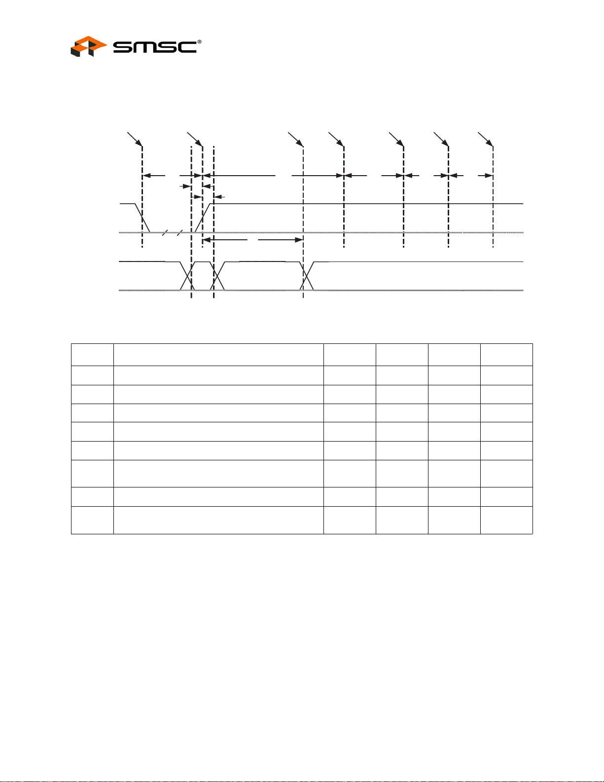
9.1.1.1 RESET_N for Strapping Option Configuration
USB MultiSwitch
Datasheet
TM
Hub
Hardware
reset
asserted
Read Strap
Options
t1
Drive Strap
Outputs to
inactive
levels
Attach
USB
Upstream
t5 t6
USB Reset
recovery
Idle
t7 t8
Start
completion
request
response
t2
Valid
t3
t4
Don’t Care
Driven by Hub if strap is an output.
RESET_N
VSS
Strap Pins
Don’t Care
VSS
Figure 9.1 Reset_N Timing for Default/Strap Option Mode
Table 9.1 Reset_N Timing for Default/Strap Option Mode
NAME DESCRIPTION MIN TYP MAX UNITS
t1 RESET_N Asserted. 1 μsec
t2 Strap Setup Time 16.7 nsec
t3 Strap Hold Time. 16.7 1400 nsec
t4 hub outputs driven to inactive logic states 1.5 2.0 μsec
t5 USB Attach (See Note 9.1) 100 msec
t6 Host acknowl edges attach and signals USB
100 msec
Reset.
t7 USB Idle. undefined mse c
t8 Completion time for requ ests (with or without d ata
5 msec
stage).
Note 9.1 When in Bus-Powered mode, the Hub and i ts associated circuitry must not consume more
than 100mA from the upstream USB power source during t1+t5.
Revision 1.91 (08-22-07) 48 SMSC USB2524
DATASHEET
Page 49

USB MultiSwitch
Datasheet
TM
Hub
9.1.1.2 RESET_N for EEPROM Configuration
Hardware
reset
asserted
Read Strap
Options
Read EEPROM
+
Set Options
Attach
USB
Upstream
USB Reset
recovery
Idle
Start
completion
request
response
t4
RESET_N
VSS
t1
t2
t3
Figure 9.2 Reset_N Timing for EEPROM Mode
Table 9.2 Reset_N Timing for EEPROM Mode
NAME DESCRIPTION MIN TYP MAX UNITS
t1 RESET_N Asserted. 1 μsec
t2 Hub Recovery/Stabilization. 500 μsec
t3 EEPROM Read / Hub Config. 2.0 99.5 msec
t5 t6 t7
t4 USB Attach (See Note 9.2) 100 msec
t5 Host acknowl edges attach and signals USB
100 msec
Reset.
t6 USB Idle. undefined mse c
t7 Completion time for requ ests (with or without d ata
5 msec
stage).
Note 9.2 When in Bus-Powered mode, the Hub and i ts associated circuitry must not consume more
than 100mA from the upstream USB power source during t4+t5+t6+ t7.
SMSC USB2524 49 Revision 1.91 (08-22-07)
DATASHEET
Page 50

9.1.1.3 RESET_N for SMBus Slave Configuration
USB MultiSwitch
Datasheet
TM
Hub
Start
completion
request
response
RESET_N
VSS
Hardware
reset
asserted
Reset
Negation
t1
SMBus Code
Load
t2 t4
Hub PHY
Stabilization
t3
Attach
USB
Upstream
USB Reset
recovery
t5
Idle
t6 t7
Figure 9.3 Reset_N Timing for SMBus Mode
T able 9.3 Reset_N Timing for SMBus Mode
NAME DESCRIPTION MIN TYP MAX UNITS
t1 RESET_N Asserted. 1 μsec
t2 Hub Recovery/Stabilization. 500 μsec
t3 SMBus Code Load (See Note 9.3) 250 300 msec
t4 Hub Configuration and USB Attach. 100 msec
t5 Host acknowledges a ttach and signals USB
100 msec
Reset.
t6 USB Idle. Undefined msec
t7 Completion time for requests (with or witho ut data
5 msec
stage).
Note: For Bus-Powe red configurations, the Hub and its associated circuitry will consume more than
100mA from the upstream USB power source during t2+t3+t4+t5+t6+t7.
Note 9.3 For Self-Powered configurations, t3 MAX is not applicable and the time to load the
configuration is determined by the external SMBus host.
9.1.2 USB Bus Reset
In response to the upstream port signaling a reset to the Hub, the Hub does the following:
Note: The Hu b does not propagate the upstream USB reset to downstream devices.
Sets default address to 0.
Sets configuration to: Unconfigured.
Negates PRTPWR[4:1] to all downstream ports.
Clears all TT buffers.
Moves device from suspended to active (if suspended).
Revision 1.91 (08-22-07) 50 SMSC USB2524
DATASHEET
Page 51

USB MultiSwitch
Datasheet
TM
Hub
Complies with Section 11.10 of the USB 2.0 Specification for behavior after completion of the reset
sequence.
The Host then configures the Hub and the Hub’s downstream port devices in accordance with the USB
Specification.
SMSC USB2524 51 Revision 1.91 (08-22-07)
DATASHEET
Page 52

Chapter 10 XNOR Test
Please contact your SMSC representative for a detailed description of how this test mode is enabled
and utilized.
USB MultiSwitch
Datasheet
TM
Hub
Revision 1.91 (08-22-07) 52 SMSC USB2524
DATASHEET
Page 53

USB MultiSwitch
Datasheet
TM
Hub
Chapter 11 DC Parameters
11.1 Maximum Guaranteed Ratings
Operating Temperature Range . . . . . . . . . . . . . . . . . . . . . . . . . . . . . . . . . . . . . . . . . . . . . . 0oC to +70oC
Storage Temperature Range. . . . . . . . . . . . . . . . . . . . . . . . . . . . . . . . . . . . . . . . . . . . . . .-55
Lead Temperature Range (soldering, 10 seconds) . . . . . . . . . . . . . . . . . . . . . . . . . . . . . . . . . . . +325
Positive Voltage on any I/O pin, with respect to Ground. . . . . . . . . . . . . . . . . . . . . . . . . . . . . . . . . 5.5V
Negative Voltage on any I/O pin, with respect to Ground. . . . . . . . . . . . . . . . . . . . . . . . . . . . . . . . .-0.V
Positive Voltage on XTAL1, with respect to Ground . . . . . . . . . . . . . . . . . . . . . . . . . . . . . . . . . . . . 4.0V
Positive Voltage on XTAL2, with respect to Ground . . . . . . . . . . . . . . . . . . . . . . . . . . . . . . . . . . . . 3.6V
Negative Voltage on XTAL1 and XTAL2, with respect to Ground. . . . . . . . . . . . . . . . . . . . . . . . . . .-0.V
o
to +150oC
o
C
Maximum V
DDA33
&V
. . . . . . . . . . . . . . . . . . . . . . . . . . . . . . . . . . . . . . . . . . . . . . . . . . . . . . . . +4.0V
DD33
*Stresses above the specified parameters could cause permanent damage to the device. This is a
stress rating only and functional ope ration of the device at any other condition above those indicated
in the operation sections of this specification is not implied.
Note: When po wering this device from laboratory or system power supplies, it is important that the
Absolute Maximum Ratings not be exceeded or device failure can result. Some power supplies
exhibit voltage spikes on their outputs when the AC power is switched on or off. In addition,
voltage transients on the AC power line may appear on the DC output. When this possibility
exists, it is suggested that a clamp circuit be used.
11.1.1 DC Electrical Characteristics
(TA = 0°C - 70°C, V
PARAMETER SYMBOL MIN TYP MAX UNITS COMMENTS
I, IS Type Input Buffer
Low Input Level
High Input Level
Input Leakage
Hysteresis (‘IS’ Only)
Input Buffer with Pull-Up
(IPU)
DD33
, V
, = +3.3 V tolerance -5% to ±10%)
DDA33
Table 11.1 DC Electrical Characteristics
V
V
ILI
V
IHI
I
IL
HYSI
2.0
-10
250 300
0.8
+10
350
V
V
uA
mV
TTL Levels
VIN = 0 to V
DD33
Low Input Level
High Input Level
Low Input Leakage
High Input Leakage
SMSC USB2524 53 Revision 1.91 (08-22-07)
V
ILI
V
IHI
I
ILL
I
IHL
2.0
0.8
10
30
V
V
uA
uA
TTL Levels
VIN = 0
VIN = V
DD33
DATASHEET
Page 54

PARAMETER SYMBOL MIN TYP MAX UNITS COMMENTS
Input Buffer with PullDown (IPD )
Table 11.1 DC Electrical Characteristics (continued)
USB MultiSwitch
Datasheet
TM
Hub
Low Input Level
High Input Level
Low Input Leakage
High Input Leakage
ICLK Input Buffer
Low Input Level
High Input Level
Input Leakage
I/OSD12 Type Buffer
Low Output Level
Output Leakage
Hysteresis
IO-U
(Note 11.2)
I-R
(Note 11.3)
Supply Current
Unconfigured
1High-Speed Hosts
1Full-Speed Hosts
V
ILI
V
IHI
I
ILL
I
IHL
V
ILCK
V
IHCK
I
IL
V
OL
I
OL
V
HYSI
I
CCINIT
I
CCINIT
2.0
1.4
-10
-10
250 300
119
117
0.8
30
10
0.5
+10
0.4
+10
350
V
V
uA
uA
V
V
uA
V
µA
mV
mA
mA
TTL Levels
VIN = 0
VIN = V
DD33
TTL Levels
VIN = 0 to V
IOL = 12 mA @ V
VIN = 0 to V
(Note 11.1)
DD33
DD33
DD33
= 3.3V
Note: 1 Upstream port is in
suspend, and the
other Upstream Port is
in the process of being
enumerated by an
external Host
controller (all
downstream ports
assigned to the
Upstream port under
enumeration).
Supply Current
Unconfigured
2 High-Speed Hosts
2 Full-Speed Hosts
Supply Current
I
CCINIT
I
CCINIT
199
174
mA
mA
Note: Both Upstream Ports
are in the process of
being enumerated by
external Host
controllers.
Total from all supplies
Configured
(2 upstream High-Speed
Hosts)
2 Ports @ FS/LS
2 Ports @ HS
1 Port HS, 1 Port FS/LS
3 Ports HS
4 Ports HS
Revision 1.91 (08-22-07) 54 SMSC USB2524
I
HCC2
I
HCH2
I
HCH1C1
I
HCH3
I
HCH4
198
260
240
310
340
mA
mA
mA
mA
mA
DATASHEET
Page 55

USB MultiSwitch
Datasheet
PARAMETER SYMBOL MIN TYP MAX UNITS COMMENTS
TM
Hub
Table 11.1 DC Electrical Characteristics (continued)
Supply Current
Total from all supplies
Configured
(2 upstream Full-Speed
Hosts)
1 Port
2 Ports
3 Ports
4 Ports
Supply Current
Suspend
Supply Current
Reset
I
FCC1
I
FCC2
I
FCC3
I
FCC4
I
CSBY
I
CRST
182
182
182
182
mA
mA
mA
mA
272 μA Total from all supplies.
73 μA Total from all supplies.
Note 11.1 Output leakage is measured with th e current pins in high impedance.
Note 11.2 See USB 2.0 Specification for USB DC electrical characteristics.
Note 11.3 RBIAS is a 3.3V tolerant analog pin.
CAPACITANCE TA = 25°C; fc = 1MHz; V
DDIO
= 3.3V
LIMITS
PARAMETER SYMBOL MIN TYP MAX UNIT TEST CONDITION
Clock Input
Capacitance
Input Capacitance C
Output Capacitance C
Power Sequencing
There are no power supply sequence restrictions for the Hub. The order in which power supplies
power-up and power-down is implementation dependent.
C
OUT
IN
IN
2 pF All pi ns except USB pins (and pins under
test tied to AC ground)
8pF
12 pF
SMSC USB2524 55 Revision 1.91 (08-22-07)
DATASHEET
Page 56

Chapter 12 AC Specifications
12.1 Oscillator/Clock
Crystal: Paralle l Resonant, Fundamental Mode, 24 MHz ±100ppm.
External Clock: 50% Duty cycle ± 10%, 24 MHz ± 100ppm, Jitter < 100ps rms.
12.1.1 SMBus Interface:
The SMSC Switching Hub conforms to all voltage, power, and timing characteristics and specifications
as set forth in the SMBus 1.0 Specification for Slave-Only devices (except as noted in Section 7.3,
"SMBus Slave Interface").
12.1.2 I2C EEPROM:
Frequency is fixed at 58.6 KHz ± 20%.
12.1.3 USB 2.0
The Hub conforms to all voltage, power, and timing characteristics and specifications as set forth in
the USB 2.0 Specification which is available at the www.usb.org web site. Please refer to the USB
Specification for more information.
USB MultiSwitch
Datasheet
TM
Hub
Revision 1.91 (08-22-07) 56 SMSC USB2524
DATASHEET
Page 57

USB MultiSwitch
Datasheet
TM
Hub
Chapter 13 Package Outline
Figure 13.1 USB2524 56-Pin QFN Pack age Outline and Parameters
SMSC USB2524 57 Revision 1.91 (08-22-07)
DATASHEET
 Loading...