

Page 1

USB2514
USB 2.0 High-Speed 4-Port
Hub Controller
PRODUCT FEATURES
General Description
The SMSC 4-Port Hub is low power, OEM configurable,
MTT (multi transaction translator) hub controller IC with
4 downstream ports for embedded USB solutions. The
4-port hub is fully compliant with the USB 2.0
Specification and will attach to an upstream port as a
Full-Speed Hub or as a Full-/High-Speed Hub. The 4Port Hub supports Low-Speed, Full-Speed, and HighSpeed (if operating as a High-Speed Hub) downstream
devices on all of the enabled downstream ports.
General Features
Hu b Controller IC with 4 downstream ports
Hi gh-performance multiple transaction translator
MultiTRAK™ Technology Provides one transaction
translator per port
Enh anced OEM configuration options available
through either a single serial i2C EEPROM, or
SMBus Slave Port
3 6-pin (6x6mm) and 48-Pin (7x7mm) QFN lead-free,
RoHS compliant packages
F ootprint compatible with USB2513 and USB2512
(36-pin QFN) to provide designers with flexibility
regarding the quantity of USB expansion ports
utilized without redesign
Hardware Features
L ow power operation
Full Power Management with individual or ganged
power control of each downstream port
On-chip Power On Reset (POR)
Interna l 1.8V Voltage Regulator
Full y integrated USB termination and Pull-up/Pull-
down resistors
On Boa rd 24MHz Crystal Driver, Resonator or
External 24/48MHz clock input
USB host/device speed indicator. Per-port 3-color
LED drivers that indicate the speed of USB host and
device connection - hi-speed (480 Mbps), full-speed
(12 Mbps), low-speed (1.5 Mbps) (48-pin QFN)
Enh anced EMI rejection and ESD protection
performance
OEM Selectable Features
Cu stomize Vendor ID, Product ID, and Device ID
Select whether the hub is part of a compound device
(When any downstream port is permanently
hardwired to a USB peripheral device, the hub is part
of a compound device)
Datasheet
Flexi ble port mapping and disable sequence. Ports
can be disabled/reordered in any order to support
multiple product SKUs. Hub will automatically reorder
the remaining ports to match the Host controller's
numbering scheme
Prog rammable USB differential-pair pin location
Ease PCB layout by aligning USB signal lines directly
to connectors
Prog rammable USB signal drive strength. Recover
USB signal integrity due to compromised system
environment using 4-level driving strength resolution
Select the presence of a permanently hardwired USB
peripheral device on a port by port basis
C onfigure the delay time for filtering the over-current
sense inputs
C onfigure the delay time for turning on downstream
port power
C onfigure the polarity of downstream port power
control signals
Indicate the maximum current that the 4-port hub
consumes from the USB upstream port
Ind icate the maximum current required for the hub
controller
Su pports Custom String Descriptor up to 31
characters in length for:
– Product String
– Manufacturer String
– Serial Number String
Pi n Selectable Options for Default Configuration
— Select Downstream Ports as Non-Removable Ports
— Select Downstream Ports as Disabled Ports
— Select Downstream Port Power Control and Over-
Current Detection on a Ganged or Individual Basis
— Select Downstream Port Power Control Polarity
— Select USB Signal Drive Strength
— Select USB Differential Pair Pin location
— Select on-chip or off-chip voltage regulator mode
Applications
L CD monitors and TVs
Multi-function USB peripherals
PC mo ther boards
Set-top b oxes, DVD players, DVR/PVR
Prin ters and scanners
PC me dia drive bay
Po rtable hub boxes
Mobile PC docking
Embedded systems
SMSC USB2514 DATASHEET Revision 1.98 (11-19-07)
Page 2

USB 2.0 High-Speed 4-Port Hub Controller
ORDER NUMBERS:
USB2514-AEZG FOR 36 PIN, QFN LEAD-FREE ROHS COMPLIANT PACKAGE
USB2514-HZH FOR 48 PIN, QFN LEAD-FREE ROHS COMPLIANT PACKAGE
Datasheet
80 ARKAY DRIVE, HAUPPAUGE, NY 11788 (631) 435-6000, FAX (631) 273-3123
Copyright © 2007 SMSC or its subsidiaries. All rights reserved.
Circuit diagrams and other information relating to SMSC products are included as a mean s of illustrating typical applications. Conse quently, complete information sufficient for
construction purposes is not necessarily given. Although the information has been checked and is believed to be accurate, no responsibility is assumed for inaccuracies. SMSC
reserves the right to make changes to specifications and product descriptions at any time without notice. Contact your local SMSC sales office to obtain the latest specifications
before placing your product order. The provision of this information does not convey to the purchaser of the described semiconductor devices any licenses under any patent
rights or other intellectual property rights of SMSC or others. All sales are expressly conditional on your agreement to the terms and conditions of the most recently da ted
version of SMSC's standard Terms of Sale Agreement dated before the date of your order (the "Terms of Sale Agreement"). The product may contain design defects or errors
known as anomalies which may cause the product's functions to deviate from published specifications. Anomaly sheets are available upon request. SMSC products are not
designed, intended, authorized or warranted for use in any life support or other application where product failure could cause or contribute to personal injury or severe property
damage. Any and all such uses without prior written approval of an Officer of SMSC and further testing and/or modification will be fully at the risk of the customer. Copies of
this document or other SMSC literature, as well as the Terms of Sale Agreement, may be obtained by visiting SMSC’s website at http://www.smsc.com. SMSC is a registered
trademark of Standard Microsystems Corporation (“SMSC”). Product names and company names are the trademarks of their respective holders.
SMSC DISCLAIMS AND EXCLUDES ANY AND ALL WARRANTIES, INCLUDING WITHOUT LIMITATION ANY AND ALL IMPLIED WARRANTIES OF MERCHANTABILITY,
FITNESS FOR A PARTICULAR PURPOSE, TITLE, AND AGAINST INFRINGEMENT AND THE LIKE, AND ANY AND ALL WARRANTIES ARISING FROM ANY COURSE
OF DEALING OR USAGE OF TRADE. IN NO EVENT SHALL SMSC BE LIABLE FOR ANY DIRECT, INCIDENTAL, INDIRECT, SPECIAL, PUNITIVE, OR CONSEQUENTIAL
DAMAGES; OR FOR LOST DATA, PROFITS, SAVINGS OR REVENUES OF ANY KIND; REGARDLESS OF THE FORM OF ACTION, WHETHER BASED ON CONTRACT;
TORT; NEGLIGENCE OF SMSC OR OTHERS; STRICT LIABILITY; BREACH OF WARRANTY; OR OTHERWISE; WHETHER OR NOT ANY REMEDY OF BUYER IS HELD
TO HAVE FAILED OF ITS ESSENTIAL PURPOSE, AND WHETHER OR NOT SMSC HAS BEEN ADVISED OF THE POSSIBILITY OF SUCH DAMAGES.
Revision 1.98 (11-19-07) 2 SMSC USB2514
DATASHEET
Page 3

USB 2.0 High-Speed 4-Port Hub Controller
Datasheet
Table of Contents
Chapter 1 Pin Configuration . . . . . . . . . . . . . . . . . . . . . . . . . . . . . . . . . . . . . . . . . . . . . . . . . . 6
Chapter 2 Block Diagram . . . . . . . . . . . . . . . . . . . . . . . . . . . . . . . . . . . . . . . . . . . . . . . . . . . . . 8
Chapter 3 Pin Descriptions . . . . . . . . . . . . . . . . . . . . . . . . . . . . . . . . . . . . . . . . . . . . . . . . . . . . 9
3.1 PIN Descriptions. . . . . . . . . . . . . . . . . . . . . . . . . . . . . . . . . . . . . . . . . . . . . . . . . . . . . . . . . . . . . . . . 9
3.2 Buffer Type Descriptions . . . . . . . . . . . . . . . . . . . . . . . . . . . . . . . . . . . . . . . . . . . . . . . . . . . . . . . . 16
Chapter 4 Configuration Options. . . . . . . . . . . . . . . . . . . . . . . . . . . . . . . . . . . . . . . . . . . . . . 18
4.1 4-Port Hub . . . . . . . . . . . . . . . . . . . . . . . . . . . . . . . . . . . . . . . . . . . . . . . . . . . . . . . . . . . . . . . . . . . 18
4.1.1 Hub Configuration Options . . . . . . . . . . . . . . . . . . . . . . . . . . . . . . . . . . . . . . . . . . . . . . . 18
4.1.2 VBus Detect. . . . . . . . . . . . . . . . . . . . . . . . . . . . . . . . . . . . . . . . . . . . . . . . . . . . . . . . . . . 18
4.2 36 QFN and 48 QFN Feature Differences . . . . . . . . . . . . . . . . . . . . . . . . . . . . . . . . . . . . . . . . . . . 18
4.3 EEPROM Interface. . . . . . . . . . . . . . . . . . . . . . . . . . . . . . . . . . . . . . . . . . . . . . . . . . . . . . . . . . . . . 19
4.3.1 Internal Register Set (Common to EEPROM and SMBus) . . . . . . . . . . . . . . . . . . . . . . . 19
4.3.2 I2C EEPROM . . . . . . . . . . . . . . . . . . . . . . . . . . . . . . . . . . . . . . . . . . . . . . . . . . . . . . . . . 34
4.3.3 In-Circuit EEPROM Programming. . . . . . . . . . . . . . . . . . . . . . . . . . . . . . . . . . . . . . . . . . 34
4.4 SMBus Slave Interface . . . . . . . . . . . . . . . . . . . . . . . . . . . . . . . . . . . . . . . . . . . . . . . . . . . . . . . . . . 35
4.4.1 Bus Protocols . . . . . . . . . . . . . . . . . . . . . . . . . . . . . . . . . . . . . . . . . . . . . . . . . . . . . . . . . 35
4.4.2 Invalid Protocol Response Behavior . . . . . . . . . . . . . . . . . . . . . . . . . . . . . . . . . . . . . . . . 36
4.4.3 General Call Address Response . . . . . . . . . . . . . . . . . . . . . . . . . . . . . . . . . . . . . . . . . . . 36
4.4.4 Slave Device Time-Out . . . . . . . . . . . . . . . . . . . . . . . . . . . . . . . . . . . . . . . . . . . . . . . . . . 36
4.4.5 Stretching the SCLK Signal. . . . . . . . . . . . . . . . . . . . . . . . . . . . . . . . . . . . . . . . . . . . . . . 36
4.4.6 SMBus Timing . . . . . . . . . . . . . . . . . . . . . . . . . . . . . . . . . . . . . . . . . . . . . . . . . . . . . . . . . 36
4.4.7 Bus Reset Sequence. . . . . . . . . . . . . . . . . . . . . . . . . . . . . . . . . . . . . . . . . . . . . . . . . . . . 37
4.4.8 SMBus Alert Response Address. . . . . . . . . . . . . . . . . . . . . . . . . . . . . . . . . . . . . . . . . . . 37
4.5 Default Configuration Option: . . . . . . . . . . . . . . . . . . . . . . . . . . . . . . . . . . . . . . . . . . . . . . . . . . . . . 37
4.6 Default Strapping Options: . . . . . . . . . . . . . . . . . . . . . . . . . . . . . . . . . . . . . . . . . . . . . . . . . . . . . . . 37
4.7 Reset . . . . . . . . . . . . . . . . . . . . . . . . . . . . . . . . . . . . . . . . . . . . . . . . . . . . . . . . . . . . . . . . . . . . . . . 38
4.7.1 Internal POR Hardware Reset. . . . . . . . . . . . . . . . . . . . . . . . . . . . . . . . . . . . . . . . . . . . . 38
4.7.2 External Hardware RESET_N . . . . . . . . . . . . . . . . . . . . . . . . . . . . . . . . . . . . . . . . . . . . . 38
4.7.3 USB Bus Reset . . . . . . . . . . . . . . . . . . . . . . . . . . . . . . . . . . . . . . . . . . . . . . . . . . . . . . . . 41
Chapter 5 DC Parameters. . . . . . . . . . . . . . . . . . . . . . . . . . . . . . . . . . . . . . . . . . . . . . . . . . . . 43
5.1 Maximum Guaranteed Ratings. . . . . . . . . . . . . . . . . . . . . . . . . . . . . . . . . . . . . . . . . . . . . . . . . . . . 43
5.2 Recommended Operating Conditions. . . . . . . . . . . . . . . . . . . . . . . . . . . . . . . . . . . . . . . . . . . . . . . 43
Chapter 6 AC Specifications. . . . . . . . . . . . . . . . . . . . . . . . . . . . . . . . . . . . . . . . . . . . . . . . . . 47
6.1 Oscillator/Clock. . . . . . . . . . . . . . . . . . . . . . . . . . . . . . . . . . . . . . . . . . . . . . . . . . . . . . . . . . . . . . . . 47
6.1.1 SMBus Interface:. . . . . . . . . . . . . . . . . . . . . . . . . . . . . . . . . . . . . . . . . . . . . . . . . . . . . . . 47
6.1.2 I2C EEPROM: . . . . . . . . . . . . . . . . . . . . . . . . . . . . . . . . . . . . . . . . . . . . . . . . . . . . . . . . . 47
6.1.3 USB 2.0 . . . . . . . . . . . . . . . . . . . . . . . . . . . . . . . . . . . . . . . . . . . . . . . . . . . . . . . . . . . . . . 47
Chapter 7 Package Outlines . . . . . . . . . . . . . . . . . . . . . . . . . . . . . . . . . . . . . . . . . . . . . . . . . . 48
SMSC USB2514 3 Revision 1.98 (11-19-07)
DATASHEET
Page 4

USB 2.0 High-Speed 4-Port Hub Controller
Datasheet
List of Figures
Figure 1.1 USB2514 36-Pin QFN . . . . . . . . . . . . . . . . . . . . . . . . . . . . . . . . . . . . . . . . . . . . . . . . . . . . . . . 6
Figure 1.2 USB2514 48-Pin QFN . . . . . . . . . . . . . . . . . . . . . . . . . . . . . . . . . . . . . . . . . . . . . . . . . . . . . . . 7
Figure 2.1 USB2514 Block Diagram . . . . . . . . . . . . . . . . . . . . . . . . . . . . . . . . . . . . . . . . . . . . . . . . . . . . . 8
Figure 4.1 Block Write. . . . . . . . . . . . . . . . . . . . . . . . . . . . . . . . . . . . . . . . . . . . . . . . . . . . . . . . . . . . . . . 35
Figure 4.2 Block Read. . . . . . . . . . . . . . . . . . . . . . . . . . . . . . . . . . . . . . . . . . . . . . . . . . . . . . . . . . . . . . . 36
Figure 4.3 LED Strapping Option . . . . . . . . . . . . . . . . . . . . . . . . . . . . . . . . . . . . . . . . . . . . . . . . . . . . . . 38
Figure 4.4 Reset_N Timing for Default/Strap Option Mode. . . . . . . . . . . . . . . . . . . . . . . . . . . . . . . . . . . 39
Figure 4.5 Reset_N Timing for EEPROM Mode . . . . . . . . . . . . . . . . . . . . . . . . . . . . . . . . . . . . . . . . . . . 40
Figure 4.6 Reset_N Timing for SMBus Mode . . . . . . . . . . . . . . . . . . . . . . . . . . . . . . . . . . . . . . . . . . . . . 41
Figure 6.1 Typical Crystal Circuit . . . . . . . . . . . . . . . . . . . . . . . . . . . . . . . . . . . . . . . . . . . . . . . . . . . . . . 47
Figure 6.2 Formula to find value of C1 and C2 . . . . . . . . . . . . . . . . . . . . . . . . . . . . . . . . . . . . . . . . . . . . 47
Figure 7.1 36-Pin QFN, 6x6mm Body, 0.5mm Pitch . . . . . . . . . . . . . . . . . . . . . . . . . . . . . . . . . . . . . . . . 48
Figure 7.2 48-Pin QFN, 7x7mm Body, 0.5mm Pitch . . . . . . . . . . . . . . . . . . . . . . . . . . . . . . . . . . . . . . . . 49
Revision 1.98 (11-19-07) 4 SMSC USB2514
DATASHEET
Page 5

USB 2.0 High-Speed 4-Port Hub Controller
Datasheet
List of Tables
Table 3.1 USB2514 Pin Descriptions . . . . . . . . . . . . . . . . . . . . . . . . . . . . . . . . . . . . . . . . . . . . . . . . . . . . 9
Table 3.2 SMBus or EEPROM Interface Behavior . . . . . . . . . . . . . . . . . . . . . . . . . . . . . . . . . . . . . . . . . 15
Table 3.3 USB2514 Power, Ground, No Connect . . . . . . . . . . . . . . . . . . . . . . . . . . . . . . . . . . . . . . . . . . 16
Table 3.4 USB2514 Buffer Type Descriptions. . . . . . . . . . . . . . . . . . . . . . . . . . . . . . . . . . . . . . . . . . . . . 16
Table 4.1 36 QFN and 48 QFN Feature Differences. . . . . . . . . . . . . . . . . . . . . . . . . . . . . . . . . . . . . . . . 18
Table 4.2 Internal Default, EEPROM and SMBus Register Memory Map. . . . . . . . . . . . . . . . . . . . . . . . 19
Table 4.3 Port Remap Register for Ports 1 & 2 . . . . . . . . . . . . . . . . . . . . . . . . . . . . . . . . . . . . . . . . . . . . 32
Table 4.4 Port Remap Register for Ports 3 & 4 . . . . . . . . . . . . . . . . . . . . . . . . . . . . . . . . . . . . . . . . . . . . 33
Table 4.5 Reset_N Timing for Default/Strap Option Mode . . . . . . . . . . . . . . . . . . . . . . . . . . . . . . . . . . . 39
Table 4.6 Reset_N Timing for EEPROM Mode . . . . . . . . . . . . . . . . . . . . . . . . . . . . . . . . . . . . . . . . . . . . 40
Table 4.7 Reset_N Timing for SMBus Mode. . . . . . . . . . . . . . . . . . . . . . . . . . . . . . . . . . . . . . . . . . . . . . 41
Table 5.1 DC Electrical Characteristics. . . . . . . . . . . . . . . . . . . . . . . . . . . . . . . . . . . . . . . . . . . . . . . . . . 44
Table 5.2 Pin Capacitance. . . . . . . . . . . . . . . . . . . . . . . . . . . . . . . . . . . . . . . . . . . . . . . . . . . . . . . . . . . . 46
SMSC USB2514 5 Revision 1.98 (11-19-07)
DATASHEET
Page 6
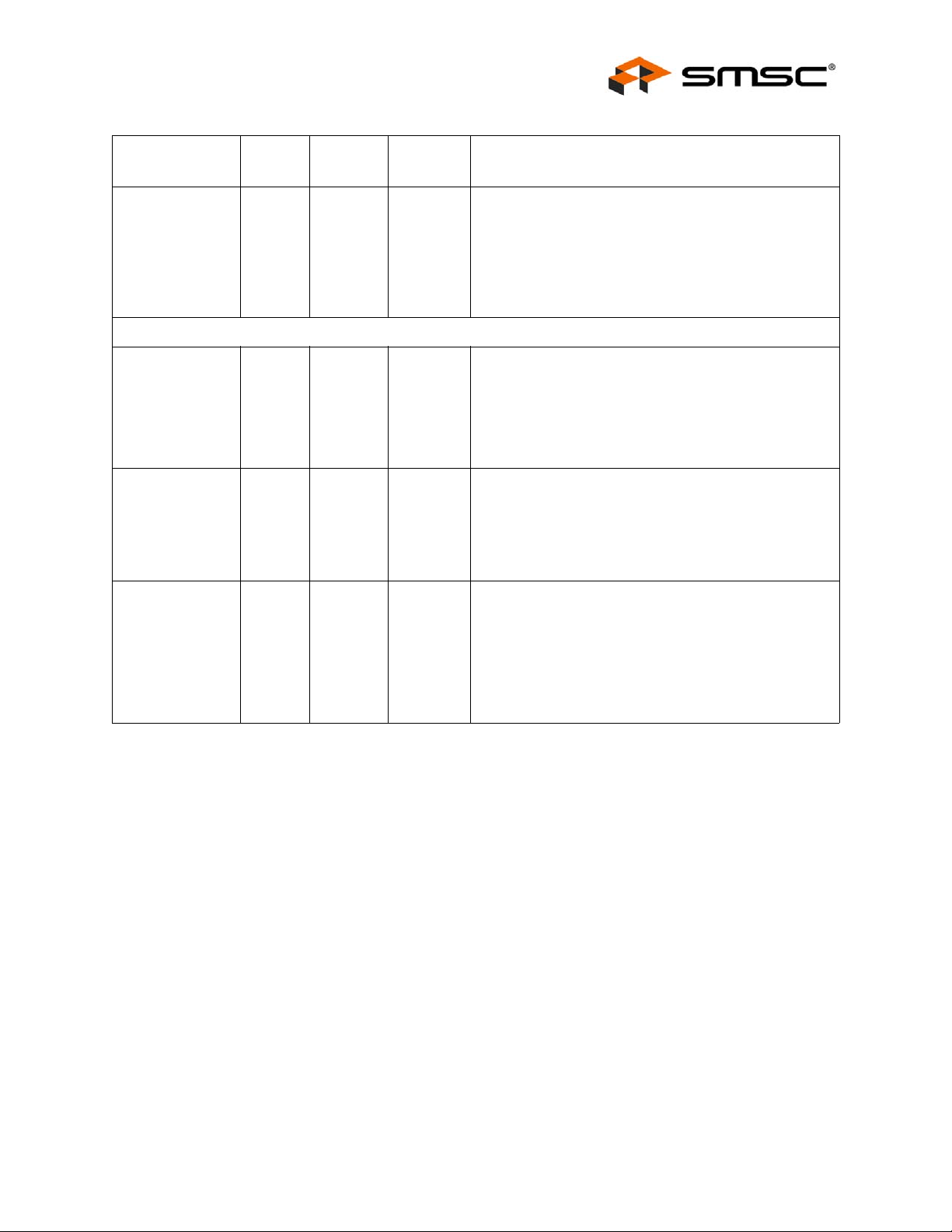
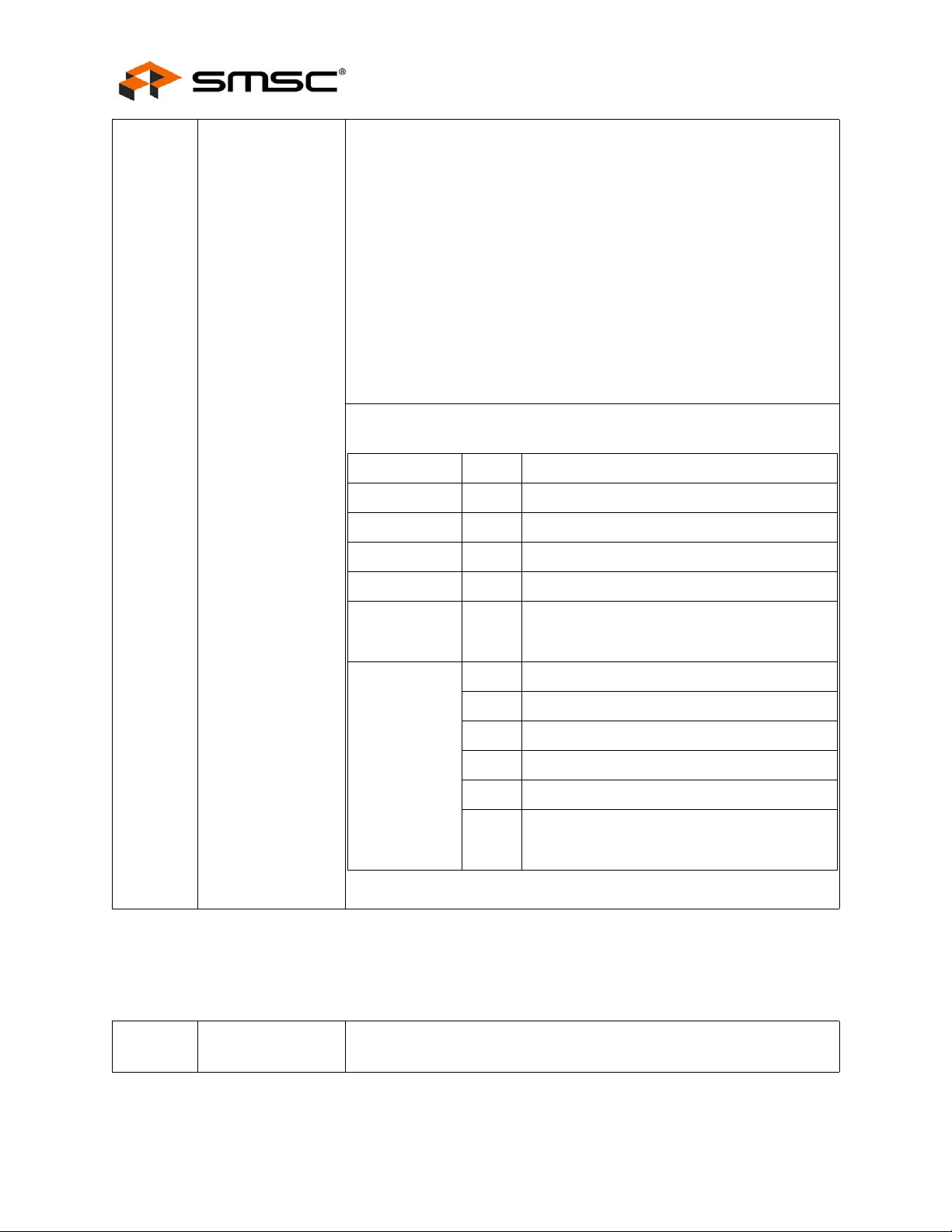
Chapter 1 Pin Configuration
USB 2.0 High-Speed 4-Port Hub Controller
Datasheet
SUSP_IND/LOCAL_PWR/NON_REM0
VDDA33
USBUP_DM
USBUP_DP
XTAL2
XTAL1/CLKIN
VDD18PLL
RBIAS
VDD33PLL
RESET_N24HS_IND/CFG_SEL123SCL/SMBCLK/CFG_SEL0
VBUS_DET
26
27
25
28
29
30
31
32
33
(Top V iew Q F N -36 )
SMSC
USB2514
34
Thermal Slug
35
(must be connected to VSS)
36
1
2
3
4
VDD33
SDA/SMBDATA/NON_REM121OCS4_N20PRTPWR4
22
5
6
VDDA33
OCS3_N
19
18
17
16
15
14
13
12
11
10
7
8
9
PRTPWR3
OCS2_N
PRTPWR2
VDD33CR
VDD18
OCS1_N
PRTPWR1
TEST
VDDA33
USBDN1_DP/PRT_DIS_P1
USBDN1_DM/PRT_DIS_M1
USBDN2_DP/PRT_DIS_P2
USBDN2_DM/PRT_DIS_M2
USBDN3_DP/PRT_DIS_P3
USBDN3_DM/PRT_DOS_M3
USBDN4_DP/PRT_DIS_P4
USBDN4_DM/PRT_DIS_M4
Indicates pins on the bottom of the device.
Figure 1.1 USB2514 36-Pin QFN
Revision 1.98 (11-19-07) 6 SMSC USB2514
DATASHEET
Page 7
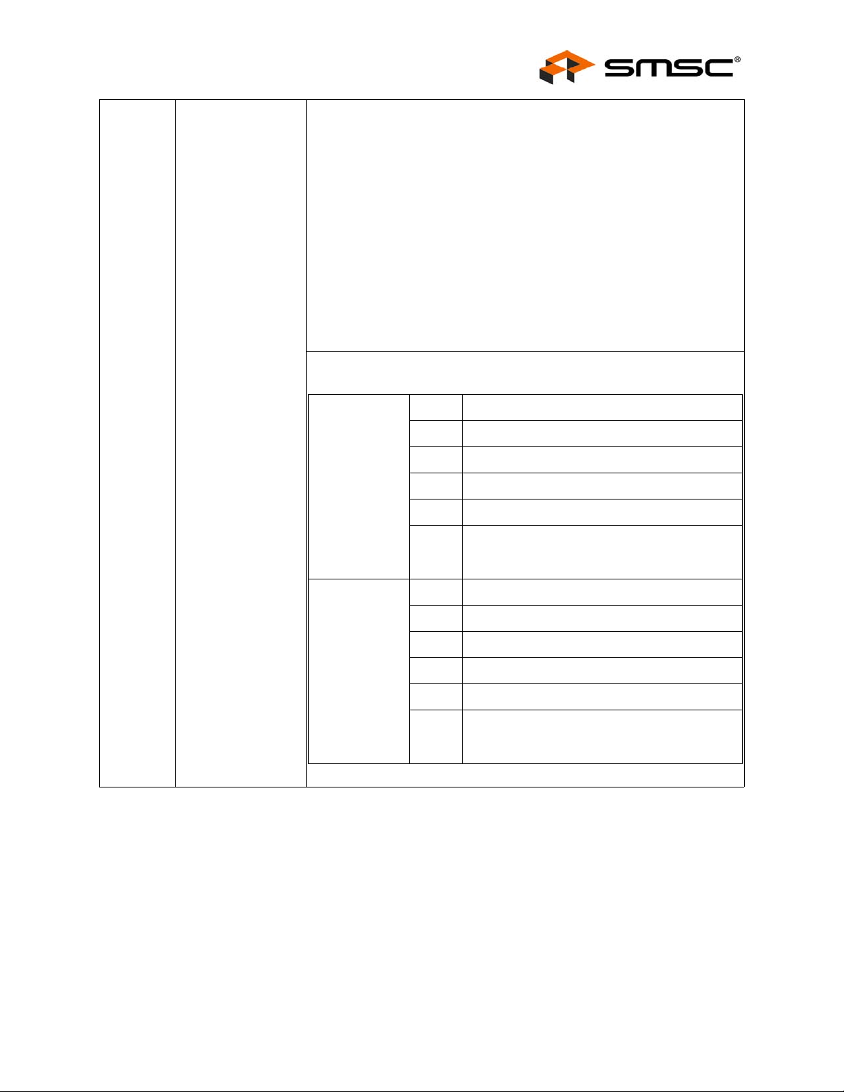
USB 2.0 High-Speed 4-Port Hub Controller
Datasheet
LED_A1_N/PRT_SWP1
PRTPWR_POL
SUSP_IND/LOCAL_PWR/NON_REM0
SEL48
VDDA33
USBUP_DM
USBUP_DP
XTAL2
XTAL1/CLKIN
VDD18PLL
RBIAS
VDD33PLL
37
38
39
40
41
42
43
44
45
46
47
48
LED_B1_N/BOOST034VBUS_DET33RESET_N
35
36
HS_IND/CFG_SEL131SCL/SMBCLK/CFG_SEL030VDD3329SDA/SMBDATA/NON_REM128OCS4_N
CFG_SEL2
32
SMSC
USB2514
(Top Vie w QFN-48 )
Thermal Slug
(must be connected to VSS)
1
2
3
4
5
VDDA33
PRTPWR426OCS3_N25LED_A2_N/PRT_SWP2
27
24
23
22
21
20
19
18
17
16
15
14
13
6
7
8
9
10
11
12
VDDA33
REG_EN
LED_B4_N
LED_B2_N/BOOS T1
LED_A3_N/PRT_SW P3
LED_B3_N/GANG_E N
PRTPWR3
OCS2_N
PRTPWR2
VDD33CR
VDD18
OCS1_N
PRTPWR1
TEST
LED_A4_N/PRT_SW P4
USBDN1_DP/PRT_DIS_P1
USBDN1_DM/PRT_DIS_M1
USBDN2_DM/PRT_DIS_M2
USBDN2_DP/PRT_DIS_P2
USBDN3_DM/PRT_DIS_M3
USBDN3_DP/PRT_DIS_P3
USBDN4_DP/PRT_DIS_P4
USBDN4_DM/PRT_DIS_M4
Indicates pins on the bottom of the device.
Figure 1.2 USB2514 48-Pin QFN
SMSC USB2514 7 Revision 1.98 (11-19-07)
DATASHEET
Page 8
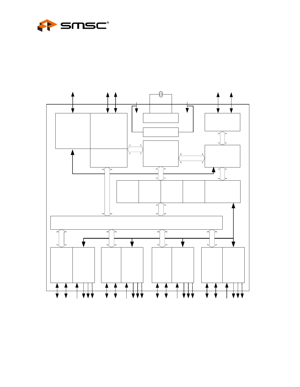
Chapter 2 Block Diagram
USB 2.0 High-Speed 4-Port Hub Controller
Datasheet
To Upstream
V
BUS
Bus-Power
Detect/V
BUS
Pulse
Upstream USB
Data
Upstream
PHY
Repeater
24 MHz Crystal
3.3V
1.8V Reg
PLL
SIE
To EEPROM or
SMBus Master
1.8V
SCKSD
Serial
Interface
Controller
TT #3TT #2TT #1
TT #4
Port
Controller
PHY#1
USB Data
Downstream
Port #1
OC
Sense
Switch
Driver
LED
Drivers
OC Sense
Switch/LED
Drivers
Routing & Port Re-Ordering Logic
Port #2
OC
PHY#2
USB Data
Downstream
Sense
Switch
Driver
LED
Drivers
OC Sense
Switch/LED
Drivers
Figure 2.1 USB2514 Block Diagram
PHY#3
USB Data
Downstream
Port #3
OC
Sense
Switch
Driver
LED
Drivers
OC Sense
Switch/LED
Drivers
PHY#4
USB Data
Downstream
Port #4
OC
Sense
Switch
Driver
LED
Drivers
OC Sense
Switch/LED
Drivers
Revision 1.98 (11-19-07) 8 SMSC USB2514
DATASHEET
Page 9
USB 2.0 High-Speed 4-Port Hub Controller
Datasheet
Chapter 3 Pin Descriptions
3.1 PIN Descriptions
This section provides a detailed description of each signal. The signals are arranged in functional
groups according to their associated interface.
The “N” symbol in the signal name indicates that the active, or asserted, state occurs when the signal
is at a low voltage level. When “N” is not present before the signal name, the signa l is asserted when
at the high voltage level.
The terms assertion and negation are used exclusively. This is done to avoid confusion when worki ng
with a mixture of “active low” and “active high” signals. The term assert, or assertion, indi cates that a
signal is active, independent of whether that level is represented by a high or low voltage. The term
negate, or negation, indicates that a signal is ina ctive.
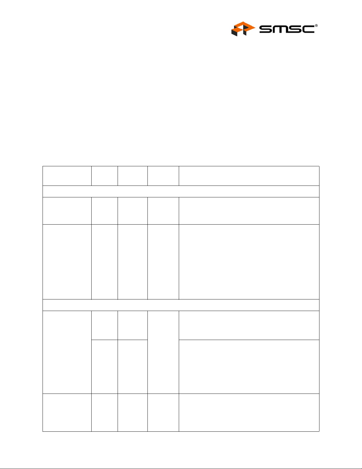
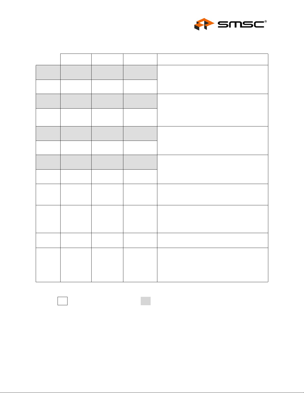
Table 3.1 USB2514 Pin Descriptions
SYMBOL 36 QFN 48 QFN
USBUP_DP
USBUP_DM
VBUS_DET 27 35 I/O12 Detect Upstream VBUS Power
USBDN_DP[4:1]/
PRT_DIS_P[4:1]
&
31
30
43
42
DOWNSTREAM 4-PORT USB 2.0 INTERFACE
9
7
4
2
9
7
4
2
BUFFER
TYPE DESCRIPTION
UPSTREAM USB INTERFACES
IO-U USB Bus Data
These pins connect to the upstream USB bus data
signals (Host port, or upstream hub).
Detects state of Upstream VBUS power . The SMSC Hub
monitors VBUS_DET to determine when to assert the
internal D+ pull-up resistor (signaling a connect event).
When designing a detachable hub, this pin must be
connected to the VBUS power pin of the USB port that
is upstream of the hub.
For self-powered applications with a permanently
attached host, this pin must be connected to 3.3V
(typically VDD33).
IO-U High-Speed USB Data & Port Disable Strap Option
These pins connect to the downstream USB peripheral
devices attached to the hub’s port.
USBDN_DM[4:1]/
PRT_DIS_M[4:1]
PRTPWR[4:1] 20
SMSC USB2514 9 Revision 1.98 (11-19-07)
8
6
3
1
18
16
12
27
21
19
15
8
6
3
1
O12 USB Power Enable
Downstream Port Disable Strap option:
If this strap is enabled by package and configuration
settings (see Table 3.2), th is pin will be sampled at
RESET_N negation to determine if the port is disabled.
Both USB data pins for the corresponding port must be
tied to the VDDA33 to disable the associated
downstream port.
Enables power to USB peripheral devices downstre am.
The active signal level of the PRTPWR[4:1] pins is
determined by the Power Polarity Strapping function of
the PRTPWR_POL pin.
DATASHEET
Page 10
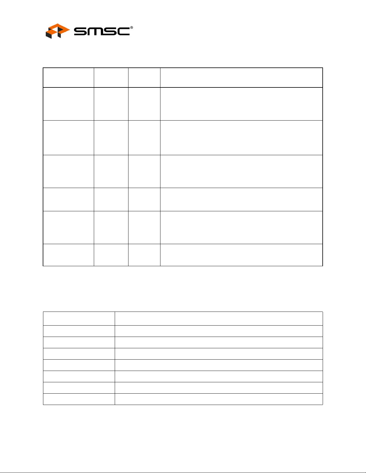
Table 3.1 USB2514 Pin Descriptions (continued)
SYMBOL 36 QFN 48 QFN
USB 2.0 High-Speed 4-Port Hub Controller
Datasheet
BUFFER
TYPE DESCRIPTION
LED_A[4:1]_N/
PRT_SWP[4:1]
n/a 13
23
25
37
I/O12 Port LED Indicators & Port Swap strapping option
Indicator LED for ports 1-4. Will be active low when LED
support is enabled via EEPROM or SMBus.
If this strap is enabled by package and configuration
settings (see Table 3.2), th is pin will be sampled at
RESET_N negation to determine the electrical
connection polarity of the downstream USB Port pins
(USB_DP and USB_DM).
Also, the active state of the LED will be determined as
follows:
‘0’ = Port Polarity is normal, and the LED is active high.
‘1’ = Port Polarity (for USB_DP and USB_DM) is
swapped, and the LED is active low.
LED_B4_N n/a 12 I/O12 Enhanced Port 4 LED
Enhanced Indicator LED for port 4. Will be active low
when LED support is enabled via EEPROM or SMBus.
LED_B3_N/
GANG_EN
n/a 22 I/O12 Enhanced Port 3 LED & Ga ng Power and Overcurrent
Strap Option
Enhanced Indicator LED for port 3. Will be active low
when LED support is enabled via EEPROM or SMBus.
GANG_EN: Selects between Gang or Individual Port
power and Over Current sensing.
LED_B[2:1]_N/
BOOST[1:0]
n/a 24
36
If this strap is enabled by package and configuration
settings (see Table 3.2), th is pin will be sampled at
RESET_N negation to determine the mode as fo llows:
‘0’ = Individual sensing & switching, and LED_B3_N is
active high.
‘1’ = Ganged sensing & switching, and LED_B3_N is
active low.
I/O12 Enhanced Port [2:1] LED & Phy Boost strapping option
Enhanced Indicator LED for ports 1 & 2. Will be active
low when LED support is enabled via EEPROM or
SMBus.
Revision 1.98 (11-19-07) 10 SMSC USB2514
DATASHEET
Page 11

USB 2.0 High-Speed 4-Port Hub Controller
Datasheet
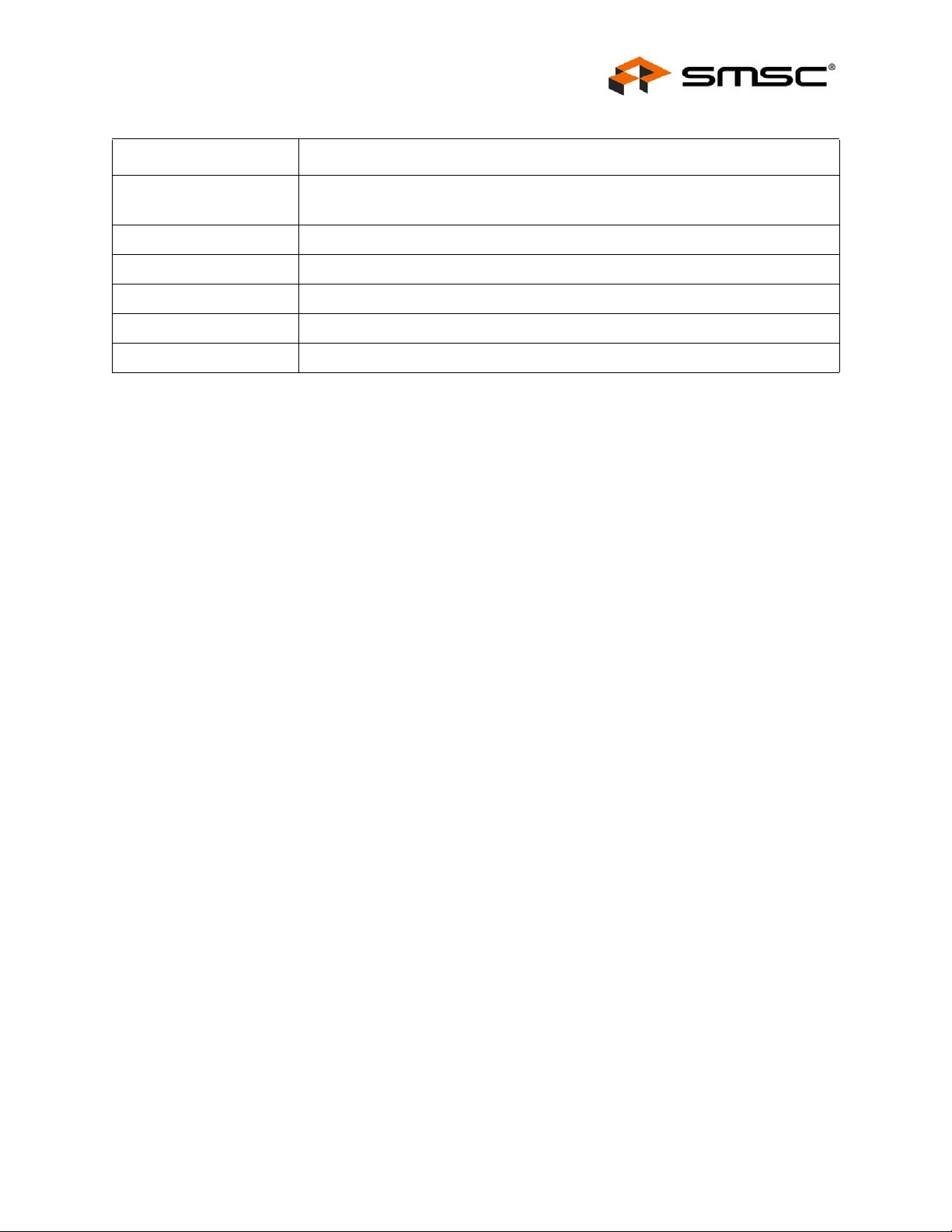
Table 3.1 USB2514 Pin Descriptions (continued)
SYMBOL 36 QFN 48 QFN
BUFFER
TYPE DESCRIPTION
BOOST[1:0], If this strap is enabled by package and
configuration settings (see Table 3.2), this pin will be
sampled at RESET_N negation to determine if all PHY
ports (upstream and downstream) operate at a normal
or boosted electrical level. Also, the active state of the
LEDs will be determined as follows:
See for BOOST values: Section 4.3.1.26, "Register F6h:
Boost_Up" and Section 4.3.1.27, "Register F8h:
Boost_4:0".
BOOST[1:0] = BOOST_IOUT[1:0]
BOOST[1:0] = ‘00’,
LED_B2_N is active high,
LED_B1_N is active high.
BOOST[1:0] = ‘01’,
LED_B2_N is active high,
LED_B1_N is active low.
BOOST[1:0] = ‘10’,
LED_B2_N is active low,
LED_B1_N is active high.
BOOST[1:0] = ‘11’,
LED_B2_N is active low,
LED_B1_N is active low.
PRTPWR_POL n/a 38 IPU Port Power Polarity strapping
Port Power Polarity strapping determination for the
active signal polarity of the [4:1]PRTPWR pins.
While RESET_N is asserted, the logic state of this pin
will (through the use of internal combinatorial logic)
determine the active state of the [4:1]PRTPWR pins in
order to ensure that downstream port power is not
inadvertently enabled to inacti ve ports during a
hardware reset.
When RESET_N is negated, the logic value will be
latched internally, and will retain the active signal polarity
for the PRTPWR[4:1] pins.
‘1’ = PRTPWR[4:1]_P/N pins have an active ‘high’
polarity
‘0’ = PRTPWR[4:1]_P/N pins have an active ‘low’
polarity
Warning: Active Low port power controllers may glitch
the downstream port power when system power is first
applied. Care should be taken when designing with
active low components!
Note: If PRTPWR_POL is not an available pin on the
package, the hub will support active high
power controllers only!
OCS[4:1]_N 21
19
17
13
SMSC USB2514 11 Revision 1.98 (11-19-07)
28
26
20
16
IPU Over Current Sense
Input from external current monitor indicating an overcurrent condition.
{Note: Contains internal pull-up to 3.3V supply}
DATASHEET
Page 12
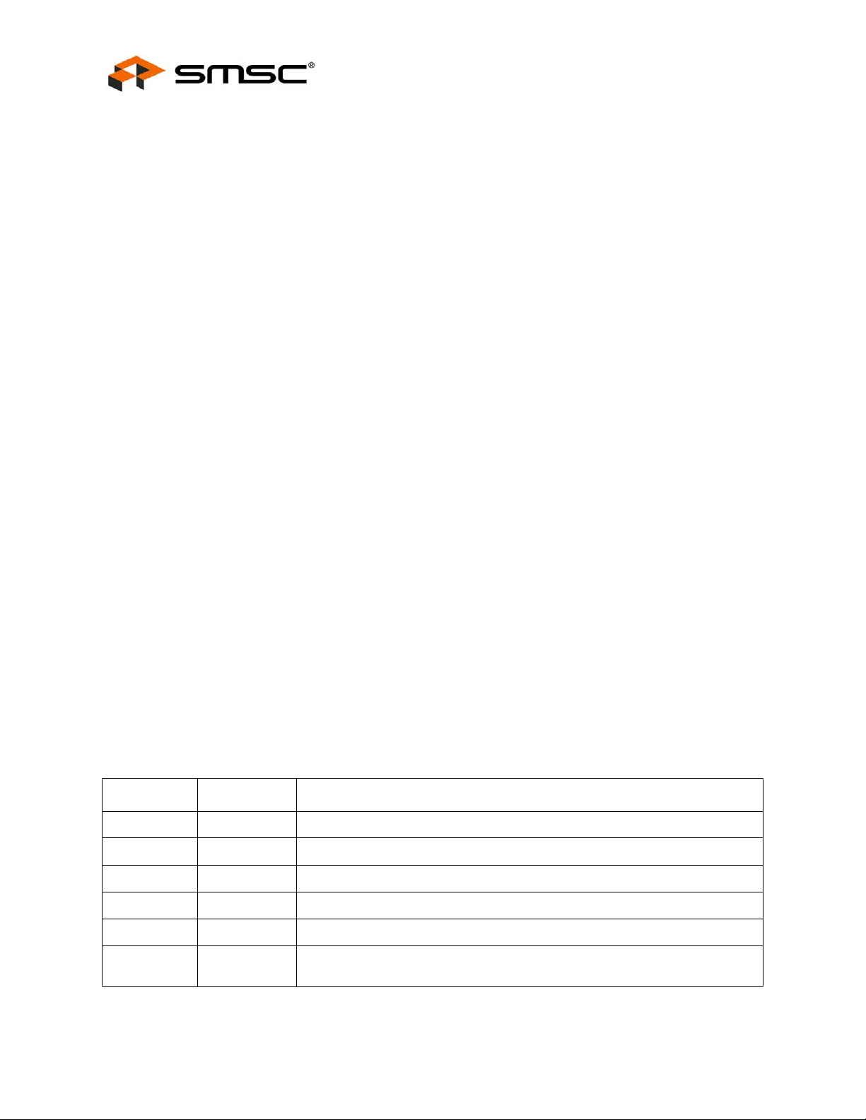
Table 3.1 USB2514 Pin Descriptions (continued)
BUFFER
SYMBOL 36 QFN 48 QFN
TYPE DESCRIPTION
RBIAS 35 47 I-R USB Transceiver Bias
A 12.0kΩ (+/- 1% ) resistor is attached from ground to
this pin to set the transceiver’s internal bias settings.
SERIAL PORT INTERFACE
USB 2.0 High-Speed 4-Port Hub Controller
Datasheet
SDA/
SMBDATA/
NON_REM1
SCL/
SMBCLK/
CFG_SEL0
HS_IND/
CFG_SEL1
22 29 I/OSD12 Serial Data / SMB Data & Port Non Removable Strap
Option
NON_REM1: Non removable port strap option.
If this strap is enabled by package and configuration
settings (see Table 3.2), th is pin will be sampled (in
conjunction with LOCAL_PWR/SUSP_IND/NON_REM0)
at RESET_N negation to determine if imports [4:1]
contain permanently attached (non-removable) devices:
NON_REM[1:0] = ‘00’, All ports are removable,
NON_REM[1:0] = ‘01’, Port 1 is nonremovable,
NON_REM[1:0] = ‘10’, Ports 1 & 2 are non-removable,
NON_REM[1:0] = ‘11’, Ports 1, 2 & 3 are non-removable
24 31 I/OSD12 Serial Clock (SCL)
SMBus Clock (SMBCLK)
Configuration Select_SEL0: The logic state of this
multifunction pin is internally latched on the rising edge
of RESET_N (RESET_N negation), and will determine
the hub configuration method as described in Table 3.2,
"SMBus or EEPROM Interface Behavior".
25 32 I/O12 High-Speed Upstream port indictor & Configuration
Programming Select
HS_IND: High Speed Indicator for upstream port
connection speed.
The active state of the LED will be determined as
follows:
CFG_SEL1 = ‘0’,
HS_IND is active high,
CFG_SEL1 = ‘1’,
HS_IND is active low,
‘Asserted’ = Hub is connected at HS
‘Negated’ = Hub is connected at FS
CFG_SEL1: The logic state of this pin is internally
latched on the rising edge of RESET_N (RESET_N
negation), and will determine the hub configuration
method as described in Table 3.2, "SMBus or EEPROM
Interface Behavior".
Revision 1.98 (11-19-07) 12 SMSC USB2514
DATASHEET
Page 13
USB 2.0 High-Speed 4-Port Hub Controller
Datasheet
Table 3.1 USB2514 Pin Descriptions (continued)
BUFFER
SYMBOL 36 QFN 48 QFN
TYPE DESCRIPTION
CFG_SEL2 n/a 33 I Configuration Programming Select
Note: This pin is not available in all packages; it is
held to a logic ‘0’ when not available
The logic state of this pin is internally latched on the
rising edge of RESET_N (RESET_N negation), and will
determine the hub configuration method as described in
Table 3.2, "SMBus or EEPROM Interface Behavior"
MISC
XTA L1/
33 45 ICLKx Crystal Input/External Clock Input
CLKIN
24MHz crystal or external clock input.
This pin connects to either one terminal of the crystal or
to an external 24/48MHz clock when a crystal is not
used.
Note: 48MHz only available in 48 QFN.
XTAL2 32 44 OCLKx Crystal Output
24MHz Crystal
This is the other terminal of the crystal, or pulled high
when an external clock source is used to drive
XTAL1/CLKIN. This output must not be used to drive
any external circuitry other than the crystal circuit.
RESET_N 26 34 IS RESET Input
The system can reset the chip by driving this input low.
The minimum active low pulse is 1 us.
When the RESET_N pin is pulled to VDD33, the internal
POR (Power on Reset) is enabled and no external reset
circuitry is required. The internal POR holds the internal
logic in reset until the power supplies are stable.
SMSC USB2514 13 Revision 1.98 (11-19-07)
DATASHEET
Page 14
Table 3.1 USB2514 Pin Descriptions (continued)
SYMBOL 36 QFN 48 QFN
USB 2.0 High-Speed 4-Port Hub Controller
Datasheet
BUFFER
TYPE DESCRIPTION
SUSP_IND/
LOCAL_PWR/
NON_REM0
28 39 I/O Active/Suspend status LED or Local-Power & Non
Removable Strap Option
Suspend Indicator: Indicates USB state of the hub.
‘negated’ = Unconfigured, or configured and in USB
Suspend
‘asserted’ = Hub is configured, and is active (i.e., not in
suspend)
Local Power: Detects availability of local self-power
source.
Low = Self/local power source is NOT available (i.e.,
Hub gets all power from Upstream USB VBus).
High = Self/local power source is available.
NON_REM0 Strap Option:
If this strap is enabled by package and configuration
settings (see Table 3.2), th is pin will be sampled (in
conjunction with NON_REM1) at RESET_N negation to
determine if ports [4:1] contain permanently attached
(non-removable) devices. Also, the active state of the
LED will be determined as follows:
NON_REM[1:0] = ‘00’, All ports are removable, and the
LED is active high
NON_REM[1:0] = ‘01’, Port 1 is nonremovable, and the
LED is active low
NON_REM[1:0] = ‘10’, Ports 1 & 2 are non-removable,
and the LED is active high
NON_REM[1:0] = ‘11’, Ports 1, 2 & 3 are nonremovable, and the LED is active low
TEST 11 14 IPD TEST pin
XNOR continuity tests all signal pins on the hub, please
contact your SMSC representative for a detailed
description of how this test mode is enabled and utilized.
SEL48 n/a 40 I Select 48 MHz clock input
48MHz external clock input select. When the hub is
clocked from an external clock source, this pin selects
either 24MHz or 48MHz mode.
‘0’ = 24MHz
‘1’ = 48MHz
REG_EN n/a 11 IPU Regulator Enable
REG_EN: This pin is internally pulled up to enable the
internal 1.8V regulators, and this pin should be treated
as a no-connect.
In order to disable the regulators, this pin will need to be
externally connected to ground.
When the internal regulator is enabled, the 1.8V power
pins must be left unconnected, except for the required
bypass capacitors.
Revision 1.98 (11-19-07) 14 SMSC USB2514
DATASHEET
Page 15
USB 2.0 High-Speed 4-Port Hub Controller
Datasheet
Table 3.2 SMBus or EEPROM Interface Behavior
CFG_SEL2 CFG_SEL1 CFG_SEL0 SMBUS OR EEPROM INTERFACE BEHAVIOR
36-Pin
QFN
48-Pin
QFN
36-Pin
QFN
48-Pin
QFN
36-Pin
QFN
48-Pin
QFN
36-Pin
QFN
48-Pin
QFN
48-Pin
QFN
48-Pin
QFN
N/A 0 0 Internal Default Configuration
Strap Options Enabled
00 0
Port Indi cators Not Supported
N/A 0 1 Configured as an SMBus slave for external download
of user-defined descriptors.
00 1
SMBus sla ve address 58 (0101100x)
Strap Options Disabled
All Settings Controlled by Registers
N/A 1 0 Internal Default Configuration
Strap Options Enabled
01 0
Bus Power Operatio n
LED Mode = USB
N/A 1 1 2-Wire I2C EEPROMS are supported.
Strap Options Disabled
01 1
All Settings Controlled by Registers
1 0 0 Internal Default Configuration
Strap Options Disabled
Dyn amic Power Switching Enabled
1 0 1 Internal Default Configuration
Strap Options Disabled
Dyn amic Power Switching Enabled
LED Mode = USB
48-Pin
QFN
48-Pin
QFN
1 1 0 Internal Default Configuration
Strap Options Disabled
1 1 1 Internal Default Configuration
Strap Options Disabled
LED Mode = USB
Gang ed Power Switching
Gang ed Over-Current Sensing
Notes:
Denotes 48-Pin QFN Denotes 36-Pin QFN
SMSC USB2514 15 Revision 1.98 (11-19-07)
DATASHEET
Page 16
USB 2.0 High-Speed 4-Port Hub Controller
Ta b le 3.3 USB2514 Power, Ground, No Connect
Datasheet
PACKAGE
SYMBOL
VDD18 14 17 VDD Core
VDD33PLL 36 48
VDDPLL18 34 46 VDD PLL
VDDA33 5
VDD33/VDD33CR 23
36 QFN 48 QFN FUNCTION
+1.8V core power. If the internal regulator is enabled, then this pin
must have a 1.0μF (or greater) ±20% (ESR <0.1Ω) capacitor to
VSS.
VDD 3.3 PLL Regulator Reference
+3.3V power supply for the PLL. If the internal PLL 1.8V regulator
is enabled, then this pin acts as the regulator input.
+1.8V Filtered analog power for internal PLL. If the internal
regulator is enabled, then this pin must have a 1.0
±20% (ESR <0.1Ω) capacitor to VSS.
10
29
15
5
10
41
30
18
VDD Analog I/O
+3.3V Filtered analog PHY power, shared between adjacent ports.
VDDIO/VDD 3.3 Core Regulator Reference
+3.3V power supply for the Digital I/O
If the internal core regulator is enabled, then VDD33CR acts as
the regulator input.
μF (or greater)
VSS n/a n/a VSS
Ground
3.2 Buffer Type Descriptions
Table 3.4 USB2514 Buffer Type Descriptions
BUFFER DESCRIPTION
I Input.
IPD Input with internal weak pull-down resistor.
IPU Input with internal weak p ull-up resistor.
IS Input with Schmitt trigger.
O12 Output 12mA.
OD12 Open drain... 12mA sink.
I/O12 Input/Output buffer with 12mA sink and 12mA source.
Revision 1.98 (11-19-07) 16 SMSC USB2514
DATASHEET
Page 17
USB 2.0 High-Speed 4-Port Hub Controller
Datasheet
Table 3.4 USB2514 Buffer Type Descriptions (continued)
BUFFER DESCRIPTION
I/OSD12
Open drain...12mA sink with Schmitt trigger, and must meet I2C-Bus Specification
Version 2.1 requirements.
ICLKx XTAL clock input.
OCLKx XTAL clock output.
I-R RBIAS.
I/O-U Analog Input/Output Defined in USB specification.
AIO Analog Input/Output.
SMSC USB2514 17 Revision 1.98 (11-19-07)
DATASHEET
Page 18
Chapter 4 Configuration Options
4.1 4-Port Hub
SMSC’s USB 2.0 4-Port Hub is fully specification compliant to the Universal Serial Bus Specification
Revision 2.0 April 27, 2000 (12/7/2000 and 5/28/2002 Errata). Please reference Chapter 10 (Hub
Specification) for general details regarding Hub operation and functionality.
For performance reasons, the 4-Port Hub provides 1 Transaction Translator (TT) per port (defined as
Multi-TT configuration), divided into 4 non-periodic buffers per TT.
4.1.1 Hub Configuration Options
The SMSC Hub supports a large number of features (some are mutually exclusive), and must be
configured in order to correctly function when attached to a USB host controller. There are three
principal ways to configure the hub: SMBus, EEPROM, or by internal default settings (with or without
pin strapping option over-rides). In all cases, the configuration method will be determined by the
CFG_SEL2, CFG_SEL1 and CFG_SEL0 pins immediately after RESET_N negation.
4.1.1.1 Power Switching Polarity
USB 2.0 High-Speed 4-Port Hub Controller
Datasheet
The selection of active state “polarity” for the PRTPWR pins is made by a strapping option only (the
PRTPWR_POL pin).
Note: If PRTPWR_POL is not an available p in on the package, the hub wi ll support a ctive high po wer
controllers only!
4.1.2 VBus Detect
According to Section 7.2.1 of the USB 2.0 Specification, a downstream port can never provide power
to its D+ or D- pull-up resistors unless the upstream port’s VBUS is in the asserted (powered) state.
The VBUS_DET pin on the Hub monitors the state of the upstream VBUS signal and will not pull-up
the D+ resistor if VBUS is not active. If VBUS goes from an active to an inactive state (Not Powered),
Hub will remove power from the D+ pull-up resistor within 10 seconds.
4.2 36 QFN and 48 QFN Feature Differences
Table 4.1 36 QFN and 48 QFN Feature Differences
36 QFN 48 QFN FEATURE
N/A Available 48MHz clock input mode
N/A Available External 1.8V regulators
N/A Available Port LED Indicators
N/A Available Port Swap Strapping Options
Available N/A Only Active High Port Power Control is supported in 36 QFN package
Available N/A Boost Default Level is used; see Table 4.2, "Internal Defa ult, EEPROM and
SMBus Register Memory Map"
Revision 1.98 (11-19-07) 18 SMSC USB2514
DATASHEET
Page 19

USB 2.0 High-Speed 4-Port Hub Controller
Datasheet
4.3 EEPROM Interface
The SMSC Hub can be configured via a 2-wire (I2C) EEPROM (256x8). (Please see Table 3.1 for
specific details on how to enable configuration via an I2C EEPROM).
The Internal state-machine will (when configured for EEPROM support) read the exte rnal EEPROM for
configuration data. The hub will then “attach” to the upstream USB host.
Note: The Hub does not have the capacity to write, or “Program,” an external EEPROM. The Hub
only has the capability to read external EEPROMs. The external eeprom will be read (even if
it is blank or non-populated), and the hub will be “configured” with the values that are read.
Please see Internal Register Set (Common to EEPROM and SMBus) for a list of data fields available.
4.3.1 Internal Register Set (Common to EEP ROM and SMBus)
Table 4.2 Internal Default, EEPROM and SMBus Register Memory Map
REG
ADDR R/W REGISTER NAME ABBR
00h R/W VID LSB VIDL 24h 0x00
INTERNAL
DEFAULT ROM
SMBUS AND
EEPROM POR
VALUES
01h R/W VID MSB VIDM 04h 0x00
02h R/W PID LSB PIDL 14h 0x00
03h R/W PID MSB PIDM 25h 0x00
04h R/W DID LSB DIDL 00h 0x00
05h R/W DID MSB DIDM 00 h 0x00
06h R/W Config Data Byte 1 CFG1 9Bh 0x00
07h R/W Config Data Byte 2 CFG2 10h 0x00
08h R/W Config Data Byte 3 CFG3 00h 0x00
09h R/W Non-Removable Devices NRD 00h 0x00
0Ah R/W Port Disable (Self) PDS 00h 0x00
0Bh R/W Port Disable (Bus) PDB 00h 0x00
0Ch R/W Max Power (Self) MAXPS 01h 0x00
0Dh R/W Max Power (Bus) MAXPB 64h 0x00
0Eh R/W Hub Controller Max Current
(Self)
0Fh R/W Hub Controller Max Current
(Bus)
HCMCS 01h 0x00
HCMCB 64h 0x00
10h R/W Power-on Time PWRT 32h 0x00
11h R/W LANG_ID_H LANGIDH 00h 0x00
12h R/W LANG_ID_L LANGIDL 00h 0x00
13h R/W MFR_STR_LEN MFRSL 00h 0x00
14h R/W PRD_STR_LEN PRDSL 00h 0x00
SMSC USB2514 19 Revision 1.98 (11-19-07)
DATASHEET
Page 20
USB 2.0 High-Speed 4-Port Hub Controller
Table 4.2 Internal Default, EEPROM and SMBus Register Memory Map (continued)
SMBUS AND
REG
ADDR R/W REGISTER NAME ABBR
15h R/W SER_STR_LEN SERSL 00h 0x00
16h-53h R/W MFR_STR MANSTR 00h 0x00
54h-91h R/W PROD_STR PRDSTR 00h 0x00
92h-Cfh R/W SER_STR SERSTR 00h 0x00
D0h-F5h R/W Reserved N/A 01h 0x00
F6h R/W Boost_Up BOOSTUP 00h 0x00
F7h R/W Reserved N/A 00h 0x00
F8h R/W Boost_4:0 BOOST40 00h 0x00
F9h R/W Reserved N/A 00h 0x00
FAh R/W Port Swap PRTSP 00h 0x00
INTERNAL
DEFAULT ROM
EEPROM POR
VALUES
Datasheet
FBh R/W Port Remap 12 PRTR12 00h 0x00
FCh R/W Port Remap 34 PRTR34 00h 0x00
FDh-FEh R/W Reserved N/A 00h 0x00
FFh R/W Status/Command
Note: SMBus register
only
STCD 00h 0x00
4.3.1.1 Register 00h: Vendor ID (LSB)
BIT
NUMBER BIT NAME DESCRIPTION
7:0 VID_LSB Least Significant Byte of the Vendor ID. This is a 16-bit value that uniquely
identifies the Vendor of the user device (assigned by USB-Interface Forum).
This field is set by the OEM using either the SMBus or EEPROM interface
options.
4.3.1.2 Register 01h: Vendor ID (MSB)
BIT
NUMBER BIT NAME DESCRIPTION
7:0 VID_MSB Most Significant Byte of the Vendor ID. This is a 16-bit value that uniquely
Revision 1.98 (11-19-07) 20 SMSC USB2514
identifies the Vendor of the user device (assigned by USB-Interface Forum).
This field is set by the OEM using either the SMBus or EEPROM interface
options.
DATASHEET
Page 21
USB 2.0 High-Speed 4-Port Hub Controller
Datasheet
4.3.1.3 Register 02h: Product ID (LSB)
BIT
NUMBER BIT NAME DESCRIPTION
7:0 PID_LSB Least Significant Byte of the Product ID. This is a 16-bit value that the Vendor
can assign that uniquely identifies this particular product (assigned by OEM).
This field is set by the OEM using either the SMBus or EEPROM interface
options.
4.3.1.4 Register 03h: Product ID (MSB)
BIT
NUMBER BIT NAME DESCRIPTION
7:0 PID_MSB Most Significant Byte of the Product ID. This is a 16-bit value that the Vendor
can assign that uniquely identifies this particular product (assigned by OEM).
This field is set by the OEM using either the SMBus or EEPROM interface
options.
4.3.1.5 Register 04h: Device ID (LSB)
BIT
NUMBER BIT NAME DESCRIPTION
7:0 DID_LSB Least Si gnificant Byte of the Device ID. This is a 16-bit device release
number in BCD format (assigned by OEM). This field is set by th e OEM
using either the SMBus or EEPROM interface options.
4.3.1.6 Register 05h: Device ID (MSB)
BIT
NUMBER BIT NAME DESCRIPTION
7:0 DID_MSB Most Significant Byte of the Device ID. Thi s is a 16-bit device release
SMSC USB2514 21 Revision 1.98 (11-19-07)
number in BCD format (assigned by OEM). This field is set by th e OEM
using either the SMBus or EEPROM interface options.
DATASHEET
Page 22

USB 2.0 High-Speed 4-Port Hub Controller
4.3.1.7 Register 06h: CONFIG_BYTE_1
BIT
NUMBER BIT NAME DESCRIPTION
7 SELF_BU S_PWR Self or Bus Power: Selects between Self- and Bus-Powered operation.
The Hub is either Self-Powered (draws less than 2mA of upstream bus
power) or Bus-Powered (limited to a 100mA maximum of upstream power
prior to being configured by the host controller).
When configured as a Bus-Powered device, the SMSC Hub consumes less
than 100mA of current prior to being configured. After configuration, the BusPowered SMSC Hub (along with all associated hub circuitry, any embedded
devices if part of a compound device, and 100mA per externally available
downstream port) must consume no more than 500mA of upstream VBUS
current. The current consumption is system dependent, and the OEM must
ensure that the USB 2.0 specifications are not violated.
When configured as a Self-Powered device, <1mA of upstream VBUS
current is consumed and all ports are available, with each port being capable
of sourcing 500mA of current.
This field is set by the OEM using either the SMBus or EEPROM interface
options.
Please see the description under Dynamic Power for the sel f/bus power
functionality when dynamic power switching is enabled.
0 = Bus-Powered operation
1 = Self-Powered operation
Note: If Dynamic Power Switching is enabled, this bit is ignored and the
LOCAL_PWR pin is used to determine if the hub is operating from
self or bus power.
Datasheet
6 Reserved Reserved
5 HS_DISABLE High Speed Disable: Disables the capability to attach as either a High/Full-
4 MTT_ENABLE Multi-TT enabl e: Enables one transaction translator per port operation.
3 EOP_DISABLE EOP Disable: Disables EOP generation of EOF1 when in Full-Speed mode.
2:1 CURRENT_SNS Over Current Sense: Selects current sensing on a port-by-port basis, all
speed device, and forces attachment as Full-speed only (i.e. no High-Speed
support).
0 = High-/Full-Speed
1 = Full-Speed-Only (High-Speed disabled!)
Selects between a mode where only one transaction translator is available
for all ports (Single-TT), or each port gets a dedicated transaction translator
(Multi-TT) {Note: The host may force Single-TT mode only}.
0 = single TT for all ports
1 = one TT per port (multiple TT’s supported)
During FS operation only, this permits the Hub to send EOP if no
downstream traffic is detected at EOF1. See Section 11.3.1 of the USB 2.0
Specification for additional details. Note: generation of an EOP at the EOF1
point may prevent a Host controller (operating in FS mode) from placing the
USB bus in suspend.
0 = EOP generation is normal
1 = EOP generation is disabled
ports ganged, or none (only for bus-powered hubs). The ability to support
current sensing on a port or ganged basis is hardware implementation
dependent.
00 = Ganged sensing (all ports together)
01 = Individual port-by-port
1x = Over current sensing not supported (must only be used with BusPowered configurations!)
Revision 1.98 (11-19-07) 22 SMSC USB2514
DATASHEET
Page 23

USB 2.0 High-Speed 4-Port Hub Controller
Datasheet
BIT
NUMBER BIT NAME DESCRIPTION
0 PORT_PWR Port Power Switching: Enables power switching on all ports simultaneously
(ganged), or port power is individually switch ed on and off on a port- by-port
basis (individual). The ability to support power enabling on a port or ganged
basis is hardware implementation dependent.
0 = Ganged switching (all ports together)
1 = Individual port-by-port switching
4.3.1.8 Register 07h: Configuration Data Byte 2
BIT
NUMBER BIT NAME DESCRIPTION
7 DYNAMIC Dynamic Power Enable: Controls the ability of the Hub to automatically
change from Self-Powered operation to Bus-Powered operation if the local
power source is removed or is unavailable (and from Bus-Powered to SelfPowered if the local power source is restored). {Note: If the local power
source is available, the Hub will always switch to Self-Powered operation.}
When Dynamic Power switching is enabled, the Hub detects the availability
of a local power source by monitoring the external LOCAL_PWR pin. If the
Hub detects a change in power source availability, the Hub immediately
disconnects and removes power from all downstream devices and
disconnects the upstream port. The Hub will then re-attach to the upstream
port as either a Bus-Powered Hub (if local-power is unavailable) or a SelfPowered Hub (if local power is available).
0 = No Dynamic auto-switching
1 = Dynamic Auto-switching capable
6 Reserved Reserved
5:4 OC_TIMER OverCurrent Timer: Over Current Timer delay.
00 = 0.1ms
01 = 4ms
10 = 8ms
11 = 1 6 m s
3 COMPOUND
Compound Device: Allows the OEM to indicate that the Hub is part
of a compound (see the USB Specification for definition) device. The
applicable port(s) must also be defined as having a "Non-Removable
Device".
Note: When configured via strapping options, declaring a port as non-
removable automatically causes the hu b controller to report that it
is part of a compound device.
0 = No
1 = Yes, Hub is part of a compound device
2:0 Reserved Reserved
SMSC USB2514 23 Revision 1.98 (11-19-07)
DATASHEET
Page 24

USB 2.0 High-Speed 4-Port Hub Controller
4.3.1.9 Register 08h: Configuration Data Byte 3
BIT
NUMBER BIT NAME DESCRIPTION
7:4 Reserved Reserved
Datasheet
3 PRTMAP_EN Port Re-ma pping enable : Selects the method used by the hub to assign port
2:1 LED_MODE LED Mode Selection: The LED_A[4:1]_N an d LED_B[4:1]_N pins support
0 STRING_EN Enables String Descriptor Support
numbers and disable ports.
‘0’ = Standard Mode
‘1’ = Port Re-map mode
several different modes of operation.
‘00’ = USB Mode
‘01’ = Speed Indication Mode
‘10’ = Same as ‘00’, USB Mode
‘11’ = Same as ‘00’, USB Mode
Warning: Do not enable an LED mode that requires LED pins that are not
available in the specific package being used in the implementation!
Note: The Hub will only report that it supports LED's to the host when
USB mode is selected. All other modes will be reported as No LED
Support.
‘0’ = String Support Disabled
‘1’ = String Support Enabled
4.3.1.10 Register 09h: Non-Removable Device
BIT
NUMBER BIT NAME DESCRIPTION
7:0 NR_DEVICE Non-Removable Device: Indicates which port(s) include non-removable
Revision 1.98 (11-19-07) 24 SMSC USB2514
devices. ‘0’ = port is removable, ‘1’ = port i s non-removable.
Informs the Host if one of the active ports has a permanent device that is
undetachable from the Hub. (Note: The device must provide its own
descriptor data.)
When using the internal default option, the NON_REM[1:0] pins will
designate the appropriate ports as being non- removable.
Bit 7= Reserved
Bit 6= Reserved
Bit 5= Reserved
Bit 4= 1; Port 4 non-removable
Bit 3= 1; Port 3 non-removable
Bit 2= 1; Port 2 non-removable
Bit 1= 1; Port 1 non removable
Bit 0 is Reserved, always = ‘0’
DATASHEET
Page 25

USB 2.0 High-Speed 4-Port Hub Controller
Datasheet
4.3.1.11 Register 0Ah: Port Disable For Self Powered Operation
BIT
NUMBER BIT NAME DESCRIPTION
7:0 PORT_DIS_SP Port Disable Self-Powered: Disables 1 or more contiguous ports. ‘0’ = port
is available, ‘1’ = port is disabled.
During Self-Powered operation when remapping mode is disable d
(PRTMAP_EN='0'), this selects the ports which will be permanently disabled,
and are not available to be enabled or enumerated by a Host Controller. The
ports can be disabled in any order, the internal logic will automatically report
the correct number of enabled ports to the USB Host, and will reorder the
active ports in order to ensure proper function.
Bit 7= Reserved
Bit 6= Reserved
Bit 5= Reserved
Bit 4= 1; Port 4 is disabled
Bit 3= 1; Port 3 is disabled
Bit 2= 1; Port 2 is disabled
Bit 1= 1; Port 1 is disabled
Bit 0 is Reserved, always = ‘0’
4.3.1.12 Register 0Bh: Port Disable For Bus Powered Operation
BIT
NUMBER BIT NAME DESCRIPTION
7:0 PORT_DIS_BP Port Disable Bus-Powered: Disables 1 or more contiguous ports. ‘0’ = port
is available, ‘1’ = port is disabled.
During Self-Powered operation when remapping mode is disabled
(PRTMAP_EN='0'), this selects the ports which will be permanently disabled,
and are not available to be enabled or enumerated by a Host Controller. The
ports can be disabled in any order, the internal logic will automatically report
the correct number of enabled ports to the USB Host, and will reorder the
active ports in order to ensure proper function.
When using the internal default option, the PRT_DIS[1:0] pins will disable the
appropriate ports.
Bit 7= Reserved
Bit 6= Reserved
Bit 5= Reserved
Bit 4= 1; Port 4 is disabled
Bit 3= 1; Port 3 is disabled
Bit 2= 1; Port 2 is disabled
Bit 1= 1; Port 1 is disabled
Bit 0 is Reserved, always = ‘0’
SMSC USB2514 25 Revision 1.98 (11-19-07)
DATASHEET
Page 26
USB 2.0 High-Speed 4-Port Hub Controller
4.3.1.13 Register 0Ch: Max Power For Self Powered Operation
BIT
NUMBER BIT NAME DESCRIPTION
Datasheet
7:0 MAX_PWR_SP Max Power Self_Powered: Value in 2mA increments that the Hub consumes
from an upstream port (VBUS) when operating as a self-powered hub. This
value includes the hub silicon along with the combi ned power consumption
(from VBUS) of all associated circuitry on the board. This value also includes
the power consumption of a permanently attached peripheral if the hub is
configured as a compound device, and the embedded peripheral reports
0mA in its descriptors.
Note: The USB 2.0 Specification does not permit this value to exceed
100mA
4.3.1.14 Register 0Dh: Max Power For Bus Powered Operation
BIT
NUMBER BIT NAME DESCRIPTION
7:0 MAX_PWR_BP Max Power Bus_Powered: Value in 2mA increments that the Hub consumes
from an upstream port (VBUS) when operating as a bus-powered hub. This
value includes the hub silicon along with the combi ned power consumption
(from VBUS) of all associated circuitry on the board. This value also includes
the power consumption of a permanently attached peripheral if the hub is
configured as a compound device, and the embedded peripheral reports
0mA in its descriptors.
4.3.1.15 Register 0Eh: Hub Controller Max Current For Self Powered Operation
BIT
NUMBER BIT NAME DESCRIPTION
7:0 HC_MAX_C_SP Hub Controller Max Current Self-Powered: Value in 2mA increments that the
Hub consumes from an upstream port (VBUS) when operating as a selfpowered hub. This value includes the hub silicon along with the combined
power consumption (from VBUS) of all associated circuitry on the board.
This value does NOT include the power consumption of a permanently
attached peripheral if the hub is configured as a compound device.
Note: The USB 2.0 Specification does not permit this value to exceed
100mA
A value of 50 (decimal) indicates 100mA, which is the default value.
Revision 1.98 (11-19-07) 26 SMSC USB2514
DATASHEET
Page 27
USB 2.0 High-Speed 4-Port Hub Controller
Datasheet
4.3.1.16 Register 0Fh: Hub Controller Max Current For Bus Powered Operation
BIT
NUMBER BIT NAME DESCRIPTION
7:0 HC_MAX_C_BP Hub Controller Max Current Bus-Powered: Value in 2mA increments that the
Hub consumes from an upstream port (VBUS) when operating as a buspowered hub. This value will include the hub silicon along with the combined
power consumption (from VBUS) of all associated circuitry on the board.
This value will NOT include the power consumption of a permanentl y
attached peripheral if the hub is configured as a compound device.
A value of 50 (decimal) would indicate 100mA, which is the default value.
4.3.1.17 Register 10h: Power-On Time
BIT
NUMBER BIT NAME DESCRIPTION
7:0 POWER_ON_TIME Power On Time: The length of time that it takes (in 2 ms intervals) from the
time the host initiated power-on sequence begins on a port until power is
good on that port.
4.3.1.18 Register 11h: Language ID High
BIT
NUMBER BIT NAME DESCRIPTION
7:0 LANG_ID_H USB LANGUAGE ID (Upper 8 bits of a 16 bit ID field)
4.3.1.19 Register 12h: Language ID Low
BIT
NUMBER BIT NAME DESCRIPTION
7:0 LANG_ID_L USB LANGUAGE ID (Lower 8 bits of a 16 bit ID field)
4.3.1.20 Register 13h: Manufacturer String Length
BIT
NUMBER BIT NAME DESCRIPTION
7:0 MFR_STR_LEN Manufacturer String Length
Maximum string length is 31 characters
SMSC USB2514 27 Revision 1.98 (11-19-07)
DATASHEET
Page 28

USB 2.0 High-Speed 4-Port Hub Controller
4.3.1.21 Register 14h: Product String Length
BIT
NUMBER BIT NAME DESCRIPTION
7:0 PRD_STR_LEN Product String Length
Maximum string length is 31 characters
4.3.1.22 Register 15h: Serial String Length
BIT
NUMBER BIT NAME DESCRIPTION
7:0 SER_STR_LEN Serial String Length
Maximum string length is 31 characters
Datasheet
4.3.1.23 Register 16h-53h: Manufacturer String
BIT
NUMBER BIT NAME DESCRIPTION
7:0 MFR_STR Manufacturer String, UNICODE UTF-16LE per USB 2.0 Specification
Maximum string length is 31 characters (62 bytes)
Note: The String consists of individual 16 Bit UNICODE UTF-16LE
characters. The Characters will be stored starting with the LSB at
the least significant address and the MSB at the next 8-bit location
(subsequent characters must be stored in sequential contig uous
address in the same LSB, MSB manner). Some EEPROM
programmers may transpose the MSB and LSB, thus reversing the
Byte order. Please pay careful attention to the Byte ordering or
your selected programming tools.
4.3.1.24 Register 54h-91h: Product String
BIT
NUMBER BIT NAME DESCRIPTION
7:0 PRD_STR Product String, UNICODE UTF-16LE per USB 2.0 Specification
Maximum string length is 31 characters (62 bytes)
Note: The String consists of individual 16 Bit UNICODE UTF-16LE
characters. The Characters will be stored starting with the LSB at
the least significant address and the MSB at the next 8-bit location
(subsequent characters must be stored in sequential contig uous
address in the same LSB, MSB manner). Some EEPROM
programmers may transpose the MSB and LSB, thus reversing the
Byte order. Please pay careful attention to the Byte ordering or
your selected programming tools.
Revision 1.98 (11-19-07) 28 SMSC USB2514
DATASHEET
Page 29
USB 2.0 High-Speed 4-Port Hub Controller
Datasheet
4.3.1.25 Register 92h-CFh: Serial String
BIT
NUMBER BIT NAME DESCRIPTION
7:0 SER_STR Serial String, UNICODE UTF16LE per USB 2.0 Specification
Maximum string length is 31 characters (62 bytes)
Note: The String consists of individual 16 Bit UNICODE UTF-16LE
characters. The Characters will be stored starting with the LSB at
the least significant address and the MSB at the next 8-bit location
(subsequent characters must be stored in sequential contig uous
address in the same LSB, MSB manner). Some EEPROM
programmers may transpose the MSB and LSB, thus reversing the
Byte order. Please pay careful attention to the Byte ordering or
your selected programming tools.
4.3.1.26 Register F6h: Boost_Up
BIT
NUMBER BIT NAME DESCRIPTION
7:2 Reserved Reserved
1:0 BOOST_IOUT Upstream USB electrical signaling drive strength Boost Bit for Upstream
Port.
‘00’ = Normal electrical drive strength = No boost
‘01’ = Elevated electrical drive strength = Low (approximately 4% b oost)
‘10’ = Elevated electrical drive strength = Medium (approximately 8% boost)
‘11’ = Elevated electrical drive strength = High (a pproximately 12% boost)
Note: “Boost” could result in non-USB Compliant parameters (one
example would be Test J/K levels), the OEM should use a ‘00’
value unless specific implementation issues require additional
signal boosting to correct for degraded USB signallin g levels.
SMSC USB2514 29 Revision 1.98 (11-19-07)
DATASHEET
Page 30

4.3.1.27 Register F8h: Boost_4:0
BIT
NUMBER BIT NAME DESCRIPTION
USB 2.0 High-Speed 4-Port Hub Controller
Datasheet
7:6 BOOST_IOUT_4 Upstream USB electrical signaling drive strength Boost Bit for Downstream
Port ‘4’.
‘00’ = Normal electrical drive strength = No boost
‘01’ = Elevated electrical drive strength = Low (approximately 4% b oost)
‘10’ = Elevated electrical drive strength = Medium (approximately 8% boost)
‘11’ = Elevated electrical drive strength = High (a pproximately 12% boost)
Note: “Boost” could result in non-USB Compliant parameters (one
example would be Test J/K levels), the OEM should use a ‘00’
value unless specific implementation issues require additional
signal boosting to correct for degraded USB signallin g levels.
5:4 BOOST_IOUT_3 Upstream USB electrical signaling drive strength Boost Bit for Downstream
Port ‘3’.
‘00’ = Normal electrical drive strength = No boost
‘01’ = Elevated electrical drive strength = Low (approximately 4% b oost)
‘10’ = Elevated electrical drive strength = Medium (approximately 8% boost)
‘11’ = Elevated electrical drive strength = High (a pproximately 12% boost)
Note: “Boost” could result in non-USB Compliant parameters (one
example would be Test J/K levels), the OEM should use a ‘00’
value unless specific implementation issues require additional
signal boosting to correct for degraded USB signallin g levels.
3:2 BOOST_IOUT_2 Upstream USB electrical signaling drive strength Boost Bit for Downstream
Port ‘2’.
‘00’ = Normal electrical drive strength = No boost
‘01’ = Elevated electrical drive strength = Low (approximately 4% b oost)
‘10’ = Elevated electrical drive strength = Medium (approximately 8% boost)
‘11’ = Elevated electrical drive strength = High (a pproximately 12% boost)
Note: “Boost” could result in non-USB Compliant parameters (one
example would be Test J/K levels), the OEM should use a ‘00’
value unless specific implementation issues require additional
signal boosting to correct for degraded USB signallin g levels.
1:0 BOOST_IOUT_1 Upstream USB electrical signaling drive strength Boost Bit for Downstream
Port ‘1’.
‘00’ = Normal electrical drive strength = No boost
‘01’ = Elevated electrical drive strength = Low (approximately 4% b oost)
‘10’ = Elevated electrical drive strength = Medium (approximately 8% boost)
‘11’ = Elevated electrical drive strength = High (a pproximately 12% boost)
Note: “Boost” could result in non-USB Compliant parameters (one
example would be Test J/K levels), the OEM should use a ‘00’
value unless specific implementation issues require additional
signal boosting to correct for degraded USB signallin g levels.
Revision 1.98 (11-19-07) 30 SMSC USB2514
DATASHEET
Page 31
USB 2.0 High-Speed 4-Port Hub Controller
Datasheet
4.3.1.28 Register FAh: Port Swap
BIT
NUMBER BIT NAME DESCRIPTION
7:0 PRTSP Port Swap: Swaps the Upstream and Downstream USB DP and DM Pins for
ease of board routing to devices and connectors.
‘0’ = USB D+ functionality is associated with the DP pin and D- functionality
is associated with the DM pin.
‘1’ = USB D+ functionality is associated with the DM pin and D- functionality
is associated with the DP pin.
Bit 7= Reserved
Bit 6= Reserved
Bit 5= Reserved
Bit 4= ‘1’; Port 4 DP/DM is Swapped.
Bit 3= ‘1’; Port 3 DP/DM is Swapped.
Bit 2= ‘1’; Port 2 DP/DM is Swapped.
Bit 1= ‘1’; Port 1 DP/DM is Swapped.
Bit 0= ‘1’; Upstream Port DP/DM is Swapped
4.3.1.29 Register FBh: Port Remap 12
BIT
NUMBER BIT NAME DESCRIPTION
SMSC USB2514 31 Revision 1.98 (11-19-07)
DATASHEET
Page 32
7:0 PRTR12 Port remap register for ports 1 & 2.
When a hub is enumerated by a USB Host Controller, the hub is only
permitted to report how many ports it has; the hub is not permitted to select
a numerical range or assignment. The Host Controller will number the
downstream ports of the hub starting with the number '1', up to the number
of ports that the hub reported having.
The host's port number is referred to as "Logical Port Number" and the
physical port on the hub is the “Physical Port Number". When remappi ng
mode is enabled (see PRTMAP_EN in Register 08h: Configuration Data
Byte 3) the hub's downstream port numbers can be remapped to different
logical port numbers (assigned by the host).
Note: The OEM must ensure that Contiguous Logical Port Numbers are
used, starting from #1 up to the maximum number of enabled ports;
this ensures that the hub's ports are numbered in accordance with
the way a Host will communicate with the ports.
Table 4.3 Port Remap Register for Ports 1 & 2
Bit [7:4] ‘0000’ Physical Port 2 is Disabled
‘0001’ Physical Port 2 is mapped to Logica l Port 1
USB 2.0 High-Speed 4-Port Hub Controller
Datasheet
‘0010’ Physical Port 2 is mapped to Logica l Port 2
‘0011’ Physical Port 2 is mapped to Logical Port 3
‘0100’ Physical Port 2 is mapped to Logica l Port 4
‘0101’
to
‘1111’
Bit [3:0] ‘0000’ Physical Port 1 is Disabled
‘0001’ Physical Port 1 is mapped to Logica l Port 1
‘0010’ Physical Port 1 is mapped to Logica l Port 2
‘0011’ Physical Port 1 is mapped to Logical Port 3
‘0100’ Physical Port 1 is mapped to Logica l Port 4
‘0101’
to
‘1111’
Illegal; Do Not Use
Illegal; Do Not Use
4.3.1.30 Register FCh: Port Remap 34
BIT
NUMBER BIT NAME DESCRIPTION
Revision 1.98 (11-19-07) 32 SMSC USB2514
DATASHEET
Page 33
USB 2.0 High-Speed 4-Port Hub Controller
Datasheet
7:0 PRTR34 Port remap register for ports 3 & 4.
When a hub is enumerated by a USB Host Controller, the hub is only
permitted to report how many ports it has; the hub is not permitted to select
a numerical range or assignment. The Host Controller will number the
downstream ports of the hub starting with the number '1', up to the number
of ports that the hub reported having.
The host's port number is referred to as "Logical Port Number" and the
physical port on the hub is the “Physical Port Number". When remappi ng
mode is enabled (see PRTMAP_EN in Register 08h: Configuration Data
Byte 3) the hub's downstream port numbers can be remapped to different
logical port numbers (assigned by the host).
Note: The OEM must ensure that Contiguous Logical Port Numbers are
used, starting from #1 up to the maximum number of enabled ports;
this ensures that the hub's ports are numbered in accordance with
the way a Host will communicate with the ports.
Table 4.4 Port Remap Register for Ports 3 & 4
Bit [7:4] ‘0000’ Physical Port 4 is Disabled
‘0001’ Physical Port 4 is mapped to Logica l Port 1
‘0010’ Physical Port 4 is mapped to Logica l Port 2
‘0011’ Physical Port 4 is mapped to Logical Port 3
‘0100’ Physical Port 4 is mapped to Logica l Port 4
‘0101’
Illegal; Do Not Use
to
‘1111’
Bit [3:0] ‘0000’ Physical Port 3 is Disabled
‘0001’ Physical Port 3 is mapped to Logica l Port 1
‘0010’ Physical Port 3 is mapped to Logica l Port 2
‘0011’ Physical Port 3 is mapped to Logical Port 3
‘0100’ Physical Port 3 is mapped to Logica l Port 4
‘0101’
Illegal; Do Not Use
to
‘1111’
SMSC USB2514 33 Revision 1.98 (11-19-07)
DATASHEET
Page 34
USB 2.0 High-Speed 4-Port Hub Controller
4.3.1.31 Register FFh: Status/Command
BIT
NUMBER BIT NAME DESCRIPTION
7:3 Reserved Reserved
2 INTF_PW_DN SMBus Interface Power Down
‘0’ = Interface is active
‘1’ = Interface power down after ACK has completed
Datasheet
1 RESET Reset the SMBus In terface and internal memory back to RESET_N
0 USB_ATTACH USB Attach (and write protect)
assertion default settings.
‘0’ = Normal Run/Idle State
‘1’ = Force a reset of registers to their default state
‘0’ = SMBus slave interface is active
‘1’ = Hub will signal a USB attach event to an upstream device, and the
internal memory (address range 00h-FEh) is “write-protected” to prevent
unintentional data corruption.
4.3.2 I2C EEPROM
The I2C EEPROM interface implements a subset of the I2C Master Specification (Please refer to the
Philips Semiconductor Standard I2C-Bus Specification for details on I2C bus protocols). The Hub’s I2C
EEPROM interface is designed to attach to a single “dedicated” I2C EEPROM, and it conforms to the
Standard-mode I2C Specification (100kbit/s transfer rate and 7-bit addressing) for protocol and
electrical compatibility.
Note: Extensions to the I2C Specification are not supported.
The Hub acts as the master and generates the serial clock SCL, contro ls the bus access (determines
which device acts as the transmitter and which device acts as the receiver), and generates the START
and STOP conditions.
4.3.2.1 Implementation Characteristics
The Hub will only access an EEPROM using the Sequential Read Protocol.
4.3.2.2 Pull-Up Resistor
The Circuit board designer is required to place external pull-up resistors (10K Ω recommended) on the
SDA/SMBDATA & SCL/SMBCLK/CFG_SELO lines (per SMBus 1.0 Specification, and EEPROM
manufacturer guidelines) to Vcc in order to assure proper operation.
4.3.2.3 I2C EEPROM Slave Address
Slave address is 1010000.
Note: 10-bit addre ssing is NOT supported.
4.3.3 In-Circuit EEPROM Programming
The EEPROM can be programmed via ATE by pulling RESET_N low (which tri-states the Hub’s
EEPROM interface and allows an external source to program the EEPROM).
Revision 1.98 (11-19-07) 34 SMSC USB2514
DATASHEET
Page 35

USB 2.0 High-Speed 4-Port Hub Controller
Datasheet
4.4 SMBus Slave Interface
Instead of loading User-Defined Descriptor data from an external EEPROM, the SMSC Hub can be
configured to receive a code load from an external processor via an SMBus interface. The SMBus
interface shares the same pins as the EEPROM interface; if CFG_SEL1 & CFG_SEL0 activates the
SMBus interface, external EEPROM support is no longer available (and the user-defined descriptor
data must be downloaded via the SMBus). Due to system issues, the SMSC Hub waits indefinitely for
the SMBus code load to complete and only “appears” as a newly connected device on USB after the
code load is complete.
The Hub’s SMBus implementation is a subset of the SMBus interface to the host. The device is a
slave-only SMBus device. The implementation in the device is a subset of SMBus since it only supports
two protocols.
The Write Block and Read Block protocols are the only valid SMBus protocols for the Hub. The Hub
responds to other protocols as described in Section 4.4.2, "In valid Protocol Response Behavior," on
page 36. Reference the System Management Bus Specification, Rev 1.0.
The SMBus interface is used to read and write the registers in the device. The register set is shown
in Section 4.3.1, "Internal Register Set (Common to EEPROM and SMBus)," on page 19.
4.4.1 Bus Protocols
Typical Write Block and Read Block protocols are shown below. Register accesses are performed
using 7-bit slave addressing, an 8-bit register address field, and an 8-bit data field. The shading
indicates the Hub driving data on the SMBDATA line; otherwise, host data is on the SDA/SMBDATA
line.
The slave address is the unique SMBus Interface Address for the Hub that identifies it on SMBus. The
register address field is the internal address of the register to be accessed. The register data field is
the data that the host is attempting to write to the register or th e contents of the register that the host
is attempting to read.
Note: Data bytes are transferred MSB first (msb first).
4.4.1.1 Block Read/Write
The Block Write begins with a slave address and a write condition. After the command co de, the host
issues a byte count which describes how many more bytes will follow in the message. If a slave had
20 bytes to send, the first byte would be the number 20 (14h), followed b y the 20 bytes of data. The
byte count may not be 0. A Block Read or Write is allowed to transfer a maximum of 32 data bytes.
Note: For the followin g SMBus tables:
Denotes Master-to-Slave Denotes Slave-to-Master
17118A1
S S lave Address Register AddressWr A
81 1 188
Byte Count = N
A Da ta b yte 1 A D a ta b y te 2
...
181
A
Data b yte N A P
Block Write
Figure 4.1 Block Write
SMSC USB2514 35 Revision 1.98 (11-19-07)
DATASHEET
Page 36

USB 2.0 High-Speed 4-Port Hub Controller
Datasheet
Block Read
A Block Read differs from a block write in that the repeated start condition exists to satisfy the I2C
specification’s requirement for a change in the transfer direction.
17118
81 1 188
Byte Count = N
Data byte 1 Data byte 2 Data byte N
Block Read
Figure 4.2 Block Read
4.4.2 Invalid Protocol Response Behavior
Registers that are accessed with an invalid protocol are not updated. A register is only updated
following a valid protocol. The only valid protocols are Write Block and Read Block, which are
described above.
The Hub only responds to the hardware selected Slave Address.
Attempting to communicate with the Hub over SMBus with an invalid slave address or invalid protocol
results in no response, and the SMBus Slave Interface returns to the idle state.
The only valid registers that are accessible by the SMBus slave address are the registers defined in
the Registers Section. See Section 4.4.3 for the response to undefined registers.
1
1
SS Slave Address Register AddressWr A
A
Slave Address Rd A
711
...
181
A AAA
P
4.4.3 General Call Address Response
The Hub does not respond to a general call address of 0000 _000b.
4.4.4 Slave Device Time-Out
According to the SMBus Specification, V1.0 devices in a transfer can abort the transfer in progress
and release the bus when any single clock low interval exceed s 25ms (T
have detected this condition must reset their communication and be able to receive a new START
condition no later than 35ms (T
Note: Some simple devices do not contain a clock low drive circuit; this simple kind of device typically
resets its communications port after a start or stop condition. The Slave Device Time-Out must
be implemented.
TIMEOUT, MAX
4.4.5 Stretching the SCLK Signal
The Hub supports stretching of the SCLK by other devices on the SMBus. The Hub does not stretch
the SCLK.
4.4.6 SMBus Timing
The SMBus Slave Interface complies with the SMBus AC Timing Specification. See the SMBus timing
in the “Timing Diagram” section.
TIMEOUT, MIN
).
). Devices that
Revision 1.98 (11-19-07) 36 SMSC USB2514
DATASHEET
Page 37

USB 2.0 High-Speed 4-Port Hub Controller
Datasheet
4.4.7 Bus Reset Sequence
The SMBus Slave Interface resets and returns to the idle state upon a START field followed
immediately by a STOP field.
4.4.8 SMBus Alert Response Address
The SMBALERT# signal is not supported by the Hub.
4.4.8.1 Undefined Registers
The registers shown in Table 4.2 are the defined registers in the Hub. Reads to undefined registers
return 00h. Writes to undefined registers have no effect and do not return an error.
4.4.8.2 Reserved Registers
Unless otherwise instructed, only a ‘0’ may be written to all reserved registers or bits.
4.5 Default Configuration Option:
The SMSC Hub can be configured via its internal default configuration. (please see Section 4.3.1,
"Internal Register Set (Common to EEPROM and SMBus)" for specific details on how to enable default
configuration.)
Please refer to Table 4.2 for the internal defau lt values that are loaded when this option is selected.
4.6 Default Strapping Options:
The USB2514 can be configured via a combination of internal de fault values and pin strap options.
Please see Table 3.1 and Table 3.2 for specific details on how to enable the default/pin-strap
configuration option.
The strapping option pins only cover a limited sub-set of the configuration options. The internal d efault
values will be used for the bits & registers that are not controlled by a strapping option pin. Please
refer to Table 4.2 for the internal default values that are loaded when this o ption is selected.
The Amber and Green LED pins are sampled after RESET_N negation, and the logic values are used
to configure the hub if the internal default co nfiguration mode is selected. The implementation shown
below (see Figure 4.3) shows a recommended passive scheme. When a pi n is co nfigured with a “Strap
High” configuration, the LED functions with active low signalling, and the PAD will “sink” the current
from the external supply. When a pin is configured with a “Strap Low” configuration, the LED functions
with active high signalling, and the PAD will “source” the current to the external LED.
SMSC USB2514 37 Revision 1.98 (11-19-07)
DATASHEET
Page 38

4.7 Reset
+V
100K
LED
Pin
HUB
LED
Pin
100K
Figure 4.3 LED Strapping Optio n
USB 2.0 High-Speed 4-Port Hub Controller
Datasheet
Strap High
LED
Strap Low
LED
There are two different resets that the Hub experiences. One is a hardware reset (either from the
internal POR reset circuit or via the RESET_N pin) and the second is a USB Bus Reset.
4.7.1 Internal POR Hardware Reset
All reset timing parameters are guaranteed by design.
4.7.2 External Hardware RESET_N
A valid hardware reset is defined as assertion of RESET_N for a minimum of 1us after all power
supplies are within operating range. While reset is asserted, the Hub (and its associated external
circuitry) consumes less than 500μA of current from the upstream USB power source.
Assertion of RESET_N (external pin) causes the following:
1. All downstream ports are disabled, and PRTPWR power to downstream devices is removed.
2. The PHYs are disabled, and the differential pairs will be in a high-impedance state.
3. All transactions immediately terminate; n o states are saved.
4. All internal registers return to the default state (in most cases, 00(h )).
5. The external crystal oscillator is halted.
6. The PLL is halted.
7. LED indicators are disa bled.
The Hub is “operational” 500μs after RESET_N is negated.
Once operational, the Hub immediately reads OEM-specific data from the external EEPROM (if the
SMBus option is not disabled).
Revision 1.98 (11-19-07) 38 SMSC USB2514
DATASHEET
Page 39
USB 2.0 High-Speed 4-Port Hub Controller
Datasheet
4.7.2.1 RESET_N for Strapping Option Configuration
Hardware
reset
asserted
Read Strap
Options
t1
Drive Strap
Outputs to
inactive
levels
Attach
USB
Upstream
t5 t6
USB Reset
recovery
Idle
t7 t8
Start
completion
request
response
t2
Valid
t3
t4
Don’t Care
Driven by Hub if strap is an output.
RESET_N
VSS
Strap Pins
Don’t Care
VSS
Figure 4.4 Reset_N Timing for Default/Strap Option Mode
Table 4.5 Reset_N Timing for Default/Strap Option Mode
NAME DESCRIPTION MIN TYP MAX UNITS
t1 RESET_N Asserted. 1 μsec
t2 Strap Setup Time 16.7 nsec
t3 Strap Hold Time. 16.7 1400 nsec
t4 hub outputs driven to inactive logic states 1.5 2 μsec
t5 USB Attach (See Note). 100 msec
t6 Host acknowledges attach and signals USB
100 msec
Reset.
t7 USB Idle. undefined msec
t8 Completion time for requests (with or without data
5 msec
stage).
Notes:
When in Bus-Powered mode, the Hub and its associated circuitry must not consume more than
100mA from the upstream USB power source during t1+t5.
All Power Supplies must have reached the operating levels mandated in Chapter 5, DC
Parameters, prior to (or coincident with) the assertion of RESET_N.
SMSC USB2514 39 Revision 1.98 (11-19-07)
DATASHEET
Page 40

4.7.2.2 RESET_N for EEPROM Configuration
USB 2.0 High-Speed 4-Port Hub Controller
Datasheet
Hardware
reset
asserted
Read Strap
Options
Read EEPROM
+
Set Options
Attach
USB
Upstream
USB Reset
recovery
Idle
Start
completion
request
response
t4
RESET_N
VSS
t1
t2
t3
Figure 4.5 Reset_N Timing for EEPROM Mode
Table 4.6 Reset_N Timing for EEPROM Mode
NAME DESCRIPTION MIN TYP MAX UNITS
t1 RESET_N Asserted. 1 μsec
t2 Hub Recovery/Stabilization. 500 μsec
t3 EEPROM Read / Hub Config. 2.0 99.5 msec
t4 USB Attach (See Note). 100 msec
t5 t6 t7
t5 Host acknowledges attach and signals USB
100 msec
Reset.
t6 USB Idle. undefined msec
t7 Completion time for requests (with or without data
5 msec
stage).
Notes:
When in Bus-Powered mode, the Hub and its associated circuitry must not consume more than
100mA from the upstream USB power source during t4+t5+t6+t7.
All Power Supplies must have reached the operating levels mandated in Chapter 5, DC
Parameters, prior to (or coincident with) the assertion of RESET_N.
Revision 1.98 (11-19-07) 40 SMSC USB2514
DATASHEET
Page 41
USB 2.0 High-Speed 4-Port Hub Controller
Datasheet
4.7.2.3 RESET_N for SMBus Slave Configuration
Start
completion
request
response
RESET_N
VSS
Hardware
reset
asserted
Reset
Negation
t1
SMBus Code
Load
t2 t4
Hub PHY
Stabilization
t3
Attach
USB
Upstream
USB Reset
recovery
t5
Idle
t6 t7
Figure 4.6 Reset_N Timing for SMBus Mode
T able 4.7 Reset_N Timing for SMBus Mode
NAME DESCRIPTION MIN TYP MAX UNITS
t1 RESET_N Asserted. 1 μsec
t2 Hub Recovery/Stabilization. 500 μsec
t3 SMBus Code Load (See Note). 250 300 msec
t4 Hub Configuration and USB Attach. 100 msec
t5 Host acknowledges attach and signals USB
100 msec
Reset.
t6 USB Idle. Undefined msec
t7 Completion time for requests (with or without data
5 msec
stage).
Notes:
For Bus-Powered configurations, the 99.5ms (MAX) i s required, and the Hub and its associated
circuitry must not consume more than 100mA from the upstream USB power source d uring
t2+t3+t4+t5+t6+t7. For Self-Powered configurations, t3 MAX is not applicable and the time to load
the configuration is determined by the external SMBus host.
All Power Supplies must have reached the operating levels mandated in Chapter 5, DC
Parameters, prior to (or coincident with) the assertion of RESET_N.
4.7.3 USB Bus Reset
In response to the upstream port signaling a reset to the Hub, the Hub does the following:
Note: The Hub does no t propagate the upstream USB reset to downstream devices.
1. Sets default address to 0.
2. Sets configuration to: Unconfigured.
3. Negates PRTPWR[4:1] to all downstream ports.
4. Clears all TT buffers.
SMSC USB2514 41 Revision 1.98 (11-19-07)
DATASHEET
Page 42

USB 2.0 High-Speed 4-Port Hub Controller
Datasheet
5. Moves device from suspended to active (if suspended).
6. Complies with Section 11.10 of the USB 2.0 Specification for behavior after completion of the reset
sequence.
The Host then configures the Hub and the Hub’s downstream port devices in accordance with the USB
Specification.
Revision 1.98 (11-19-07) 42 SMSC USB2514
DATASHEET
Page 43
USB 2.0 High-Speed 4-Port Hub Controller
Datasheet
Chapter 5 DC Parameters
5.1 Maximum Guaranteed Ratings
PARAMETER SYMBOL MIN MAX UNITS COMMENTS
Storage
Temperature
Lead
Temperature
1.8V supply
voltage
3.3V supply
voltage
Voltage on any
I/O pin
Voltage on
XTAL1
Voltage on
XTAL2
Note: Stresses above the specified parameters could cause permanent damage to the device. This
T
A
-55 150 °C
325 °C Soldering < 10 seconds
V
DDA18PLL,
V
DD18
V
DDA33,
V
DD33PLL,
V
DD33,
V
DD33CR
2.5 V
4.6 V
-0.5 5.5 V
-0.5 4.0 V
-0.5 3.6 V
is a stress rating only and functional operation of the device at any condition above those
indicated in the operation sections of this specification is not implied. When powering this
device from laboratory or system power supplies, it is important that the Absolute Maximum
Ratings not be exceeded or device failure can result. Some power supplies exhibit voltage
spikes on their outputs when the AC power is switched on or off. In addition, voltage transients
on the AC power line may appear on the DC output. When this possibi lity exists, it is suggested
that a clamp circuit be used.
5.2 Recommended Operating Conditions
PARAMETER SYMBOL MIN MAX UNITS COMMENTS
Operating
Temperature
1.8V supply voltage V
3.3V supply voltage V
Voltage on any I/O pin -0.3 5.5 V If any 3.3V supply voltage drops
SMSC USB2514 43 Revision 1.98 (11-19-07)
T
A
DDA18PLL
V
DD18
DDA33
V
DDA33PLL
V
DD33
V
DD33CR
070°C
1.62 1.98 V
3.0 3.6 V
below 3.0V, then the MAX
becomes:
(3.3V supply voltage) + 0.5
DATASHEET
Page 44

USB 2.0 High-Speed 4-Port Hub Controller
PARAMETER SYMBOL MIN MAX UNITS COMMENTS
Datasheet
Voltage on XTAL1 -0.3 V
Voltage on XTAL2 -0.3 V
DDA33
DD18
V
V
Table 5.1 DC Electrical Characteristics
PARAMETER SYMBOL MIN TYP MAX UNITS COMMENTS
I, IS Type Input Buffer
Low Input Level
High Input Level
Input Leakage
Hysteresis (‘IS’ Only)
V
V
V
IHI
I
IL
HYSI
ILI
0.8
2.0
-10
250
+10
350
V
V
uA
mV
TTL Levels
VIN = 0 to V
Input Buffer with Pull-Up
(IPU)
Low Input Level
High Input Level
Low Input Leakage
High Input Leakage
V
ILI
V
IHI
I
ILL
I
IHL
2.0
+35
-10
0.8
+90
+10
uA
uA
V
V
TTL Levels
VIN = 0
VIN = V
Input Buffer with PullDown (IPD)
DD33
DD33
Low Input Level
High Input Level
Low Input Leakage
High Input Leakage
ICLK Input Buffer
Low Input Level
High Input Level
Input Leakage
O12, I/O12 &I/OSD12
Type Buffer
Low Output Level
High Output Level
Output Leakage
Hysteresis (‘SD’ pad only)
V
V
I
I
V
V
V
V
I
V
HYSC
ILI
IHI
ILL
IHL
ILCK
IHCK
I
IL
OL
OH
OL
2.0
+10
-35
1.4
-10
2.4
-10
250
0.8
-10
-90
0.5
+10
0.4
+10
350
V
V
uA
uA
V
V
uA V
V
V
uA
mV
TTL Levels
VIN = 0
VIN = V
= 0 to V
IN
DD33
DD33
IOL = 12mA @ V
IOH = -12mA @ V
V
= 0 to V
IN
(Note 5.1)
DD33
DD33
DD33
= 3.3V
= 3.3V
Revision 1.98 (11-19-07) 44 SMSC USB2514
DATASHEET
Page 45

USB 2.0 High-Speed 4-Port Hub Controller
Datasheet
Table 5.1 DC Electrical Characteristics (con tinued)
PARAMETER SYMBOL MIN TYP MAX UNITS COMMENTS
IO-U
(Note 5.2)
Supply Current
Unconfigured
High-Speed Host
Full-Speed Host
Supply Current
Configured
(High-Speed Host)
1 Port HS, 1 Port LS/FS
2 Ports @ LS/FS
2 Ports @ HS
3 Ports @ HS
4 Ports @ HS
Supply Current
Configured
(Full-Speed Host)
1 Port
2 Ports
3 Ports
4 Ports
Supply Current
Suspend
Supply Current
Reset
Note 5.1 Output leakage is measured with the current pins in high impedance.
Note 5.2 See USB 2.0 Specification for USB DC electrical characteristics.
I
CCINTHS
I
CCINITFS
I
HCH1C1
I
HCC2
I
HCH2
I
HCH3
I
HCH4
I
FCC1
I
FCC2
I
FCC3
I
FCC4
I
CSBY
I
CRST
95
80
105
90
mA
mA
All supplies combined
150
150
160
170
175
170
160
275
290
305
mA
mA
mA
mA
mA
All supplies combined
140
140
140
140
150
150
150
150
mA
mA
mA
mA
310 420 μA A ll supplies combined
100 275 μA A ll supplies combined
SMSC USB2514 45 Revision 1.98 (11-19-07)
DATASHEET
Page 46

USB 2.0 High-Speed 4-Port Hub Controller
Datasheet
CAPACITANCE TA = 25°C; fc = 1MHz; V
DD18
, V
DDPLL
= 1.8V
Table 5.2 Pin Capacitance
LIMITS
PARAMETER SYMBOL MIN TYP MAX UNIT TEST CONDITION
Clock Input
Capacitance
Input Capacitance C
Output Capacitance C
C
XTAL
IN
OUT
2 pF All pins except USB pins (and pins under
test tied to AC ground)
10 pF
20 pF
Revision 1.98 (11-19-07) 46 SMSC USB2514
DATASHEET
Page 47

USB 2.0 High-Speed 4-Port Hub Controller
Datasheet
Chapter 6 AC Specifications
6.1 Oscillator/Clock
Crystal: Paralle l Resonant, Fundamental Mode, 24 MHz ±350ppm.
External Clock: 50% Duty cycle ± 10%, 24/48 MHz ± 350ppm, Jitter < 100ps rms.
C
1
XTAL1
(C
CB + C
S1 =
XTAL
)
Crystal
C
2
Figure 6.1 Typical Crystal Circuit
Note: CB equals total board/trace capacitance.
C
(C1 + CS1) x (C2 + CS2)
(C
+ CS1 + C2 + CS2)
1
Figure 6.2 Formula to find value of C
L
1M eg
C
=
and C
1
XTAL2
(C
S2 =
CB + C
L
2
XTAL
)
6.1.1 SMBus Interface:
The SMSC Hub conforms to all voltage, power, and timing characteristics and specifications as set
forth in the SMBus 1.0 Specification for Slave-Only devices (except as noted in Section 4.4, "SMBus
Slave Interface").
6.1.2 I2C EEPROM:
Frequency is fixed at 58.6KHz ± 20%.
6.1.3 USB 2.0
The SMSC Hub conforms to all voltage, power, and timing characteristics and specifications as set
forth in the USB 2.0 Specification. Please refer to the USB 2.0 Specification for more information.
SMSC USB2514 47 Revision 1.98 (11-19-07)
DATASHEET
Page 48
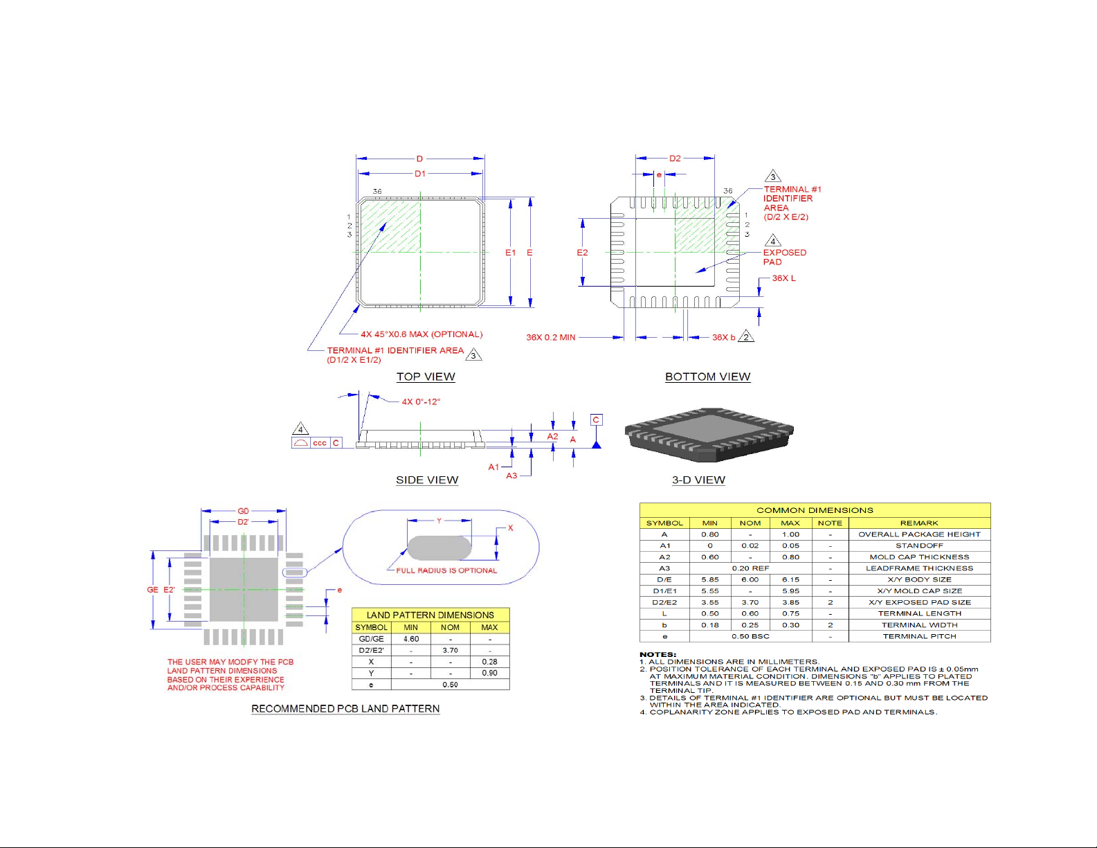
Chapter 7 Package Outlines
Datasheet
USB 2.0 High-Speed 4-Port Hub Controller
DATASHEET
Figure 7.1 36-Pin QFN, 6x6mm B ody, 0.5mm Pitch
SMSC USB2514 48 Revision 1.98 (11-19-07)
Page 49

USB 2.0 High-Speed 4-Port Hub Controller
Datasheet
DATASHEET
Figure 7.2 48-Pin QFN, 7x7mm B ody, 0.5mm Pitch
SMSC USB2514 49 Revision 1.98 (11-19-07)
 Loading...