

Page 1

USB2512/12A/12B
USB2513/13B
USB2514/14B
USB2517
USB 2.0 Hi-Speed
Hub Controller
PRODUCT FEATURES
General Description
The SMSC USB251x hub is a family of low-power, OEM
configurable, MTT (multi transaction translator)
controller IC products for embedded USB solutions. The
“x” in the part number indicates the number of
downstream ports available. The SMSC hub supports
low-speed, full-speed, and hi-speed (if operating as a hispeed hub) downstream devices on all of the enabled
downstream ports.
For a summary of the products documented in this
datasheet, please refer to the Chapter 1, "USB251x Hub
Family Differences Overview," on page 7.
Highlights
High performance, low-power, small footprint hub
controller IC with 2, 3, 4, or 7 downstream ports
(indicated by the “x” in the part number)
Fully compliant with the USB 2.0 specification
Enhanced OEM configuration options available
through either a single serial I
SMBus slave port
MultiTRAK
— High-performance multiple transaction translator which
PortMap
— Flexible port mapping and disable sequencing
PortSwap
— Programmable USB differential-pair pin locations ease
PHYBoost
— Programmable USB signal drive strength for recovering
TM
provides one transaction translator per port
PCB design by aligning USB signal lines directly to
connectors
signal integrity using 4-level driving strength resolution
2C®
EEPROM, or
1
hub
Datasheet
Features
Full power management with individual or ganged
power control of each downstream port
Fully integrated USB termination and pull-up/pull-
down resistors
Supports a single external 3.3 V supply source;
internal regulators provide 1.2 V or 1.8 V internal
core voltage
On-chip driver for 24 MHz crystal resonator or
external 24/48 MHz clock input
Customizable vendor ID, product ID, and device ID
ESD protection up to 4 kilovolts on all USB pins
Supports self- or bus-powered operation
USB251xB
2
and USB251xBi products support the
USB Battery Charging specification
Lead-free RoHS compliant packages:
— 36-pin QFN (6x6 mm)
— 48-pin QFN (7x7 mm)
— 64-pin QFN (9x9 mm)
USB251xi, USB2512Ai, and USB251xBi products
support the industrial temperature range of -40ºC
to +85ºC
Applications
LCD monitors and TVs
Multi-function USB peripherals
PC motherboards
Set-top boxes, DVD players, DVR/PVR
Printers and scanners
PC media drive bay
Portable hub boxes
Mobile PC docking
Embedded systems
2.USB251xB and USB251xBi products are not yet available.
The information in this datasheet regarding USB251xB/Bi
1.USB2512A/Ai only uses a single transaction translator.
SMSC USB251x Hub Family DATASHEET Revision 1.0 (3-11-09)
serves as a preliminary product preview.
Page 2
ORDER NUMBERS
ORDER NUMBERS:
LEAD-FREE
ROHS COMPLIANT
PACKAGE PACKAGE SIZE
USB 2.0 Hi-Speed Hub Controller
Datasheet
TEMPERATURE
RANGE
USB2512-AEZG
USB2512A-AEZG
USB2512B-AEZG
USB2513-AEZG
USB2513B-AEZG
USB2514-AEZG
USB2514B-AEZG
USB2512i-AEZG
USB2512Ai-AEZG
USB2512Bi-AEZG
USB2513i-AEZG
USB2513Bi-AEZG
USB2514i-AEZG
USB2514Bi-AEZG
USB2513-HZH
USB2514-HZH
USB2517-JZX
USB2517i-JZX
Note: USB251xB/USB251xBi products have not yet been released. They
36QFN 6 x 6 x 0.5 mm 0ºC to 70ºC
36QFN 6 x 6 x 0.5 mm -40ºC to 85ºC
48QFN 7 x 7 x 0.5 mm 0ºC to 70ºC
64QFN 9 x 9 x 0.5 mm 0ºC to 70ºC
64QFN 9 x 9 x 0.5 mm -40ºC to 85ºC
are featured in this datasheet as a preliminary product preview.
80 ARKAY DRIVE, HAUPPAUGE, NY 11788 (631) 435-6000, FAX (631) 273-3123
Copyright © 2009 SMSC or its subsidiaries. All rights reserved.
Circuit diagrams and other information relating to SMSC products are included as a means of illustrating typical applications. Consequently, complete information sufficient for
construction purposes is not necessarily given. Although the information has been checked and is believed to be accurate, no responsibility is assumed for inaccuracies. SMSC
reserves the right to make changes to specifications and product descriptions at any time without notice. Contact your local SMSC sales office to obtain the latest specifications
before placing your product order. The provision of this information does not convey to the purchaser of the described semiconductor devices any licenses under any patent
rights or other intellectual property rights of SMSC or others. All sales are expressly conditional on your agreement to the terms and conditions of the most recently dated
version of SMSC's standard Terms of Sale Agreement dated before the date of your order (the "Terms of Sale Agreement"). The product may contain design defects or errors
known as anomalies which may cause the product's functions to deviate from published specifications. Anomaly sheets are available upon request. SMSC products are not
designed, intended, authorized or warranted for use in any life support or other application where product failure could cause or contribute to personal injury or severe property
damage. Any and all such uses without prior written approval of an Officer of SMSC and further testing and/or modification will be fully at the risk of the customer. Copies of
this document or other SMSC literature, as well as the Terms of Sale Agreement, may be obtained by visiting SMSC’s website at http://www.smsc.com. SMSC is a registered
trademark of Standard Microsystems Corporation (“SMSC”). Product names and company names are the trademarks of their respective holders.
SMSC DISCLAIMS AND EXCLUDES ANY AND ALL WARRANTIES, INCLUDING WITHOUT LIMITATION ANY AND ALL IMPLIED WARRANTIES OF MERCHANTABILITY,
FITNESS FOR A PARTICULAR PURPOSE, TITLE, AND AGAINST INFRINGEMENT AND THE LIKE, AND ANY AND ALL WARRANTIES ARISING FROM ANY COURSE
OF DEALING OR USAGE OF TRADE. IN NO EVENT SHALL SMSC BE LIABLE FOR ANY DIRECT, INCIDENTAL, INDIRECT, SPECIAL, PUNITIVE, OR CONSEQUENTIAL
DAMAGES; OR FOR LOST DATA, PROFITS, SAVINGS OR REVENUES OF ANY KIND; REGARDLESS OF THE FORM OF ACTION, WHETHER BASED ON CONTRACT;
TORT; NEGLIGENCE OF SMSC OR OTHERS; STRICT LIABILITY; BREACH OF WARRANTY; OR OTHERWISE; WHETHER OR NOT ANY REMEDY OF BUYER IS HELD
TO HAVE FAILED OF ITS ESSENTIAL PURPOSE, AND WHETHER OR NOT SMSC HAS BEEN ADVISED OF THE POSSIBILITY OF SUCH DAMAGES.
Revision 1.0 (3-11-09) 2 SMSC USB251x
DATASHEET
Page 3

USB 2.0 Hi-Speed Hub Controller
Datasheet
Table of Contents
Chapter 1 USB251x Hub Family Differences Overview . . . . . . . . . . . . . . . . . . . . . . . . . . . . 7
Chapter 2 General Description. . . . . . . . . . . . . . . . . . . . . . . . . . . . . . . . . . . . . . . . . . . . . . . . . 8
Chapter 3 Acronyms . . . . . . . . . . . . . . . . . . . . . . . . . . . . . . . . . . . . . . . . . . . . . . . . . . . . . . . . 10
Chapter 4 Block Diagram . . . . . . . . . . . . . . . . . . . . . . . . . . . . . . . . . . . . . . . . . . . . . . . . . . . . 11
Chapter 5 Pin Descriptions . . . . . . . . . . . . . . . . . . . . . . . . . . . . . . . . . . . . . . . . . . . . . . . . . . . 12
5.1 Pin Configurations and Lists (Organized by Package Type) . . . . . . . . . . . . . . . . . . . . . . . . . . . . . 12
5.2 USB251x Pin Descriptions (Grouped by Function). . . . . . . . . . . . . . . . . . . . . . . . . . . . . . . . . . . . . 22
5.3 Buffer Type Descriptions . . . . . . . . . . . . . . . . . . . . . . . . . . . . . . . . . . . . . . . . . . . . . . . . . . . . . . . . 27
Chapter 6 LED Usage Description . . . . . . . . . . . . . . . . . . . . . . . . . . . . . . . . . . . . . . . . . . . . . 29
6.1 LED Functionality . . . . . . . . . . . . . . . . . . . . . . . . . . . . . . . . . . . . . . . . . . . . . . . . . . . . . . . . . . . . . . 29
6.1.1 USB Mode 14-Wire . . . . . . . . . . . . . . . . . . . . . . . . . . . . . . . . . . . . . . . . . . . . . . . . . . . . . 29
6.1.2 LED Mode Speed Indication . . . . . . . . . . . . . . . . . . . . . . . . . . . . . . . . . . . . . . . . . . . . . . 29
Chapter 7 Battery Charging Support . . . . . . . . . . . . . . . . . . . . . . . . . . . . . . . . . . . . . . . . . . 31
7.1 General Description . . . . . . . . . . . . . . . . . . . . . . . . . . . . . . . . . . . . . . . . . . . . . . . . . . . . . . . . . . . . 31
7.2 USB Battery Charging . . . . . . . . . . . . . . . . . . . . . . . . . . . . . . . . . . . . . . . . . . . . . . . . . . . . . . . . . . 31
7.2.1 Special Behavior of PRTPWR Pins . . . . . . . . . . . . . . . . . . . . . . . . . . . . . . . . . . . . . . . . . 31
7.3 Battery Charging Configuration . . . . . . . . . . . . . . . . . . . . . . . . . . . . . . . . . . . . . . . . . . . . . . . . . . . 32
7.3.1 Battery Charging enabled via EEPROM or SMBus. . . . . . . . . . . . . . . . . . . . . . . . . . . . . 32
Chapter 8 Configuration Options. . . . . . . . . . . . . . . . . . . . . . . . . . . . . . . . . . . . . . . . . . . . . . 33
8.1 Hub . . . . . . . . . . . . . . . . . . . . . . . . . . . . . . . . . . . . . . . . . . . . . . . . . . . . . . . . . . . . . . . . . . . . . . . . . 33
8.1.1 Hub Configuration Options . . . . . . . . . . . . . . . . . . . . . . . . . . . . . . . . . . . . . . . . . . . . . . . 33
8.1.2 SMBus or EEPROM Interface . . . . . . . . . . . . . . . . . . . . . . . . . . . . . . . . . . . . . . . . . . . . . 33
8.1.3 VBus Detect. . . . . . . . . . . . . . . . . . . . . . . . . . . . . . . . . . . . . . . . . . . . . . . . . . . . . . . . . . . 34
8.2 EEPROM Interface . . . . . . . . . . . . . . . . . . . . . . . . . . . . . . . . . . . . . . . . . . . . . . . . . . . . . . . . . . . . . 34
8.2.1 Internal Register Set (Common to EEPROM and SMBus) . . . . . . . . . . . . . . . . . . . . . . . 35
8.2.2 I
8.2.3 In-Circuit EEPROM Programming . . . . . . . . . . . . . . . . . . . . . . . . . . . . . . . . . . . . . . . . . . 52
8.3 SMBus Slave Interface . . . . . . . . . . . . . . . . . . . . . . . . . . . . . . . . . . . . . . . . . . . . . . . . . . . . . . . . . . 53
8.3.1 SMBus Slave Addresses . . . . . . . . . . . . . . . . . . . . . . . . . . . . . . . . . . . . . . . . . . . . . . . . . 53
8.3.2 Bus Protocols . . . . . . . . . . . . . . . . . . . . . . . . . . . . . . . . . . . . . . . . . . . . . . . . . . . . . . . . . 53
8.3.3 Invalid Protocol Response Behavior . . . . . . . . . . . . . . . . . . . . . . . . . . . . . . . . . . . . . . . . 54
8.3.4 General Call Address Response . . . . . . . . . . . . . . . . . . . . . . . . . . . . . . . . . . . . . . . . . . . 54
8.3.5 Slave Device Time-Out . . . . . . . . . . . . . . . . . . . . . . . . . . . . . . . . . . . . . . . . . . . . . . . . . . 54
8.3.6 Stretching the SCLK Signal . . . . . . . . . . . . . . . . . . . . . . . . . . . . . . . . . . . . . . . . . . . . . . . 54
8.3.7 SMBus Timing . . . . . . . . . . . . . . . . . . . . . . . . . . . . . . . . . . . . . . . . . . . . . . . . . . . . . . . . . 54
8.3.8 Bus Reset Sequence. . . . . . . . . . . . . . . . . . . . . . . . . . . . . . . . . . . . . . . . . . . . . . . . . . . . 54
8.3.9 SMBus Alert Response Address . . . . . . . . . . . . . . . . . . . . . . . . . . . . . . . . . . . . . . . . . . . 55
8.4 Default Configuration Option: . . . . . . . . . . . . . . . . . . . . . . . . . . . . . . . . . . . . . . . . . . . . . . . . . . . . . 55
8.5 Default Strapping Options: . . . . . . . . . . . . . . . . . . . . . . . . . . . . . . . . . . . . . . . . . . . . . . . . . . . . . . . 55
8.6 Reset . . . . . . . . . . . . . . . . . . . . . . . . . . . . . . . . . . . . . . . . . . . . . . . . . . . . . . . . . . . . . . . . . . . . . . . 55
8.6.1 External Hardware RESET_N . . . . . . . . . . . . . . . . . . . . . . . . . . . . . . . . . . . . . . . . . . . . . 55
8.6.2 USB Bus Reset . . . . . . . . . . . . . . . . . . . . . . . . . . . . . . . . . . . . . . . . . . . . . . . . . . . . . . . . 58
2
C EEPROM. . . . . . . . . . . . . . . . . . . . . . . . . . . . . . . . . . . . . . . . . . . . . . . . . . . . . . . . . . 52
Chapter 9 DC Parameters. . . . . . . . . . . . . . . . . . . . . . . . . . . . . . . . . . . . . . . . . . . . . . . . . . . . 60
SMSC USB251x 3 Revision 1.0 (3-11-09)
DATASHEET
Page 4

USB 2.0 Hi-Speed Hub Controller
Datasheet
9.1 Maximum Guaranteed Ratings . . . . . . . . . . . . . . . . . . . . . . . . . . . . . . . . . . . . . . . . . . . . . . . . . . . . 60
9.2 Operating Conditions . . . . . . . . . . . . . . . . . . . . . . . . . . . . . . . . . . . . . . . . . . . . . . . . . . . . . . . . . . . 60
Chapter 10 AC Specifications . . . . . . . . . . . . . . . . . . . . . . . . . . . . . . . . . . . . . . . . . . . . . . . . . . 66
10.1 Oscillator/Clock. . . . . . . . . . . . . . . . . . . . . . . . . . . . . . . . . . . . . . . . . . . . . . . . . . . . . . . . . . . . . . . . 66
10.1.1 SMBus Interface: . . . . . . . . . . . . . . . . . . . . . . . . . . . . . . . . . . . . . . . . . . . . . . . . . . . . . . . 66
10.1.2 I
2
C EEPROM: . . . . . . . . . . . . . . . . . . . . . . . . . . . . . . . . . . . . . . . . . . . . . . . . . . . . . . . . . 66
10.1.3 USB 2.0 . . . . . . . . . . . . . . . . . . . . . . . . . . . . . . . . . . . . . . . . . . . . . . . . . . . . . . . . . . . . . . 66
Chapter 11 Package Outlines . . . . . . . . . . . . . . . . . . . . . . . . . . . . . . . . . . . . . . . . . . . . . . . . . . 67
11.1 Tape and Reel Specifications . . . . . . . . . . . . . . . . . . . . . . . . . . . . . . . . . . . . . . . . . . . . . . . . . . . . . 70
Revision 1.0 (3-11-09) 4 SMSC USB251x
DATASHEET
Page 5

USB 2.0 Hi-Speed Hub Controller
Datasheet
List of Tables
Table 1.1 36-pin QFN (6x6x0.5 mm) RoHS Compliant Part Numbers . . . . . . . . . . . . . . . . . . . . . . . . . . . 7
Table 1.2 48-pin QFN (7x7x0.5 mm) RoHS Compliant Part Numbers . . . . . . . . . . . . . . . . . . . . . . . . . . . 7
Table 1.3 64-pin QFN (9x9x0.5 mm) RoHS Compliant Part Numbers . . . . . . . . . . . . . . . . . . . . . . . . . . . 7
Table 5.1 Pin List in Alphabetical Order . . . . . . . . . . . . . . . . . . . . . . . . . . . . . . . . . . . . . . . . . . . . . . . . . 18
Table 5.2 USB251x Pin Descriptions. . . . . . . . . . . . . . . . . . . . . . . . . . . . . . . . . . . . . . . . . . . . . . . . . . . . 22
Table 5.3 Buffer Type Descriptions . . . . . . . . . . . . . . . . . . . . . . . . . . . . . . . . . . . . . . . . . . . . . . . . . . . . . 27
Table 8.1 Hub Configuration Options . . . . . . . . . . . . . . . . . . . . . . . . . . . . . . . . . . . . . . . . . . . . . . . . . . . 33
Table 8.2 Internal Default, EEPROM and SMBus Register Memory Map . . . . . . . . . . . . . . . . . . . . . . . . 35
Table 8.3 PortMap Register for Ports 1 & 2 . . . . . . . . . . . . . . . . . . . . . . . . . . . . . . . . . . . . . . . . . . . . . . . 48
Table 8.4 PortMap Register for Ports 3 & 4 . . . . . . . . . . . . . . . . . . . . . . . . . . . . . . . . . . . . . . . . . . . . . . . 49
Table 8.5 PortMap Register for Ports 5 & 6 . . . . . . . . . . . . . . . . . . . . . . . . . . . . . . . . . . . . . . . . . . . . . . . 50
Table 8.6 PortMap Register for Port 7 . . . . . . . . . . . . . . . . . . . . . . . . . . . . . . . . . . . . . . . . . . . . . . . . . . . 51
Table 8.7 Reset_N Timing for Default/Strap Option Mode . . . . . . . . . . . . . . . . . . . . . . . . . . . . . . . . . . . 56
Table 8.8 Reset_N Timing for EEPROM Mode . . . . . . . . . . . . . . . . . . . . . . . . . . . . . . . . . . . . . . . . . . . . 57
Table 8.9 Reset_N Timing for SMBus Mode . . . . . . . . . . . . . . . . . . . . . . . . . . . . . . . . . . . . . . . . . . . . . . 58
Table 9.1 DC Electrical Characteristics . . . . . . . . . . . . . . . . . . . . . . . . . . . . . . . . . . . . . . . . . . . . . . . . . . 61
Table 9.2 Pin Capacitance. . . . . . . . . . . . . . . . . . . . . . . . . . . . . . . . . . . . . . . . . . . . . . . . . . . . . . . . . . . . 65
SMSC USB251x 5 Revision 1.0 (3-11-09)
DATASHEET
Page 6

USB 2.0 Hi-Speed Hub Controller
Datasheet
List of Figures
Figure 4.1 USB251x Hub Family Block Diagram . . . . . . . . . . . . . . . . . . . . . . . . . . . . . . . . . . . . . . . . . . 11
Figure 5.1 2-Port 36-Pin QFN . . . . . . . . . . . . . . . . . . . . . . . . . . . . . . . . . . . . . . . . . . . . . . . . . . . . . . . . . 12
Figure 5.2 3-Port 36-pin QFN . . . . . . . . . . . . . . . . . . . . . . . . . . . . . . . . . . . . . . . . . . . . . . . . . . . . . . . . . 13
Figure 5.3 4-Port 36-pin QFN . . . . . . . . . . . . . . . . . . . . . . . . . . . . . . . . . . . . . . . . . . . . . . . . . . . . . . . . . 14
Figure 5.4 3-Port 48-Pin QFN . . . . . . . . . . . . . . . . . . . . . . . . . . . . . . . . . . . . . . . . . . . . . . . . . . . . . . . . . 15
Figure 5.5 4-Port 48-Pin QFN . . . . . . . . . . . . . . . . . . . . . . . . . . . . . . . . . . . . . . . . . . . . . . . . . . . . . . . . . 16
Figure 5.6 7-Port 64-Pin QFN . . . . . . . . . . . . . . . . . . . . . . . . . . . . . . . . . . . . . . . . . . . . . . . . . . . . . . . . . 17
Figure 6.1 Dual Color LED Implementation Example . . . . . . . . . . . . . . . . . . . . . . . . . . . . . . . . . . . . . . . 29
Figure 7.1 Battery Charging via External Power Supply . . . . . . . . . . . . . . . . . . . . . . . . . . . . . . . . . . . . . 31
Figure 8.1 Block Write . . . . . . . . . . . . . . . . . . . . . . . . . . . . . . . . . . . . . . . . . . . . . . . . . . . . . . . . . . . . . . . 53
Figure 8.2 Block Read. . . . . . . . . . . . . . . . . . . . . . . . . . . . . . . . . . . . . . . . . . . . . . . . . . . . . . . . . . . . . . . 54
Figure 8.3 Reset_N Timing for Default/Strap Option Mode. . . . . . . . . . . . . . . . . . . . . . . . . . . . . . . . . . . 56
Figure 8.4 Reset_N Timing for EEPROM Mode . . . . . . . . . . . . . . . . . . . . . . . . . . . . . . . . . . . . . . . . . . . 57
Figure 8.5 Reset_N Timing for SMBus Mode . . . . . . . . . . . . . . . . . . . . . . . . . . . . . . . . . . . . . . . . . . . . . 58
Figure 9.1 Supply Rise Time Model . . . . . . . . . . . . . . . . . . . . . . . . . . . . . . . . . . . . . . . . . . . . . . . . . . . . 61
Figure 10.1 Typical Crystal Circuit . . . . . . . . . . . . . . . . . . . . . . . . . . . . . . . . . . . . . . . . . . . . . . . . . . . . . . 66
Figure 10.2 Formula to Find the Value of C1 and C2 . . . . . . . . . . . . . . . . . . . . . . . . . . . . . . . . . . . . . . . . 66
Figure 10.3 Simplified Form of the Capacitance Formula . . . . . . . . . . . . . . . . . . . . . . . . . . . . . . . . . . . . . 66
Figure 11.1 36-Pin QFN, 6x6 mm Body, 0.5 mm Pitch . . . . . . . . . . . . . . . . . . . . . . . . . . . . . . . . . . . . . . . 67
Figure 11.2 48-Pin QFN, 7x7 mm Body, 0.5 mm Pitch . . . . . . . . . . . . . . . . . . . . . . . . . . . . . . . . . . . . . . . 68
Figure 11.3 64-Pin QFN, 9x9 mm Body, 0.5 mm Pitch . . . . . . . . . . . . . . . . . . . . . . . . . . . . . . . . . . . . . . . 69
Figure 11.4 36-Pin Package Tape Specifications . . . . . . . . . . . . . . . . . . . . . . . . . . . . . . . . . . . . . . . . . . . 70
Figure 11.5 48-Pin Package Tape Specifications . . . . . . . . . . . . . . . . . . . . . . . . . . . . . . . . . . . . . . . . . . . 71
Figure 11.6 36-Pin and 48-Pin Package Reel Specifications . . . . . . . . . . . . . . . . . . . . . . . . . . . . . . . . . . 72
Revision 1.0 (3-11-09) 6 SMSC USB251x
DATASHEET
Page 7
USB 2.0 Hi-Speed Hub Controller
Datasheet
Chapter 1 USB251x Hub Family Differences Overview
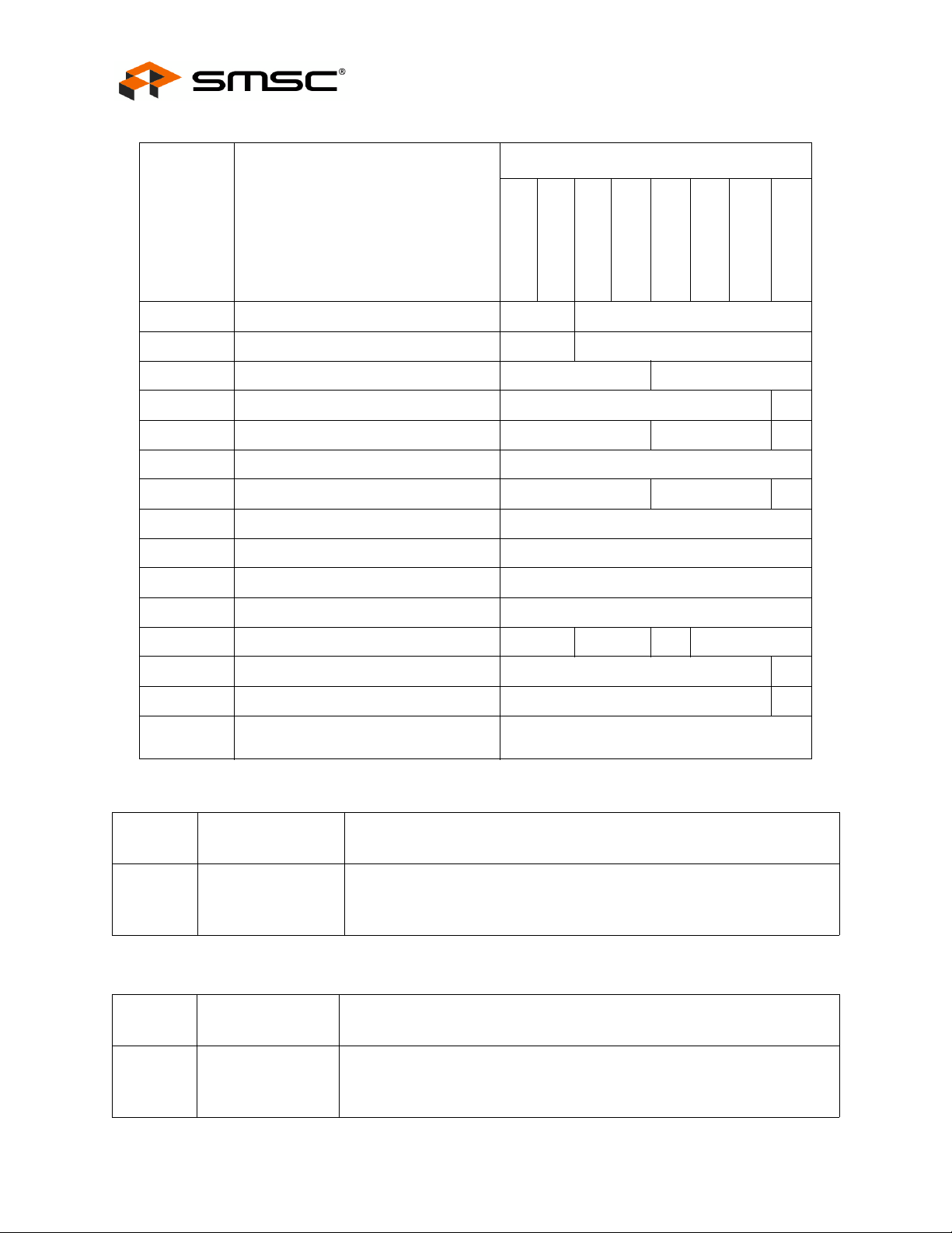
Table 1.1 36-pin QFN (6x6x0.5 mm) RoHS Compliant Part Numbers
Part
Number
USB2512
USB2512A
USB2512B
USB2512i
USB2512Bi
USB2512Ai
USB2513
USB2513B
USB2513i
USB2513Bi
USB2514
USB2514B
USB2514i
USB2514Bi
Downstream
ports
Table 1.2 48-pin QFN (7x7x0.5 mm) RoHS Compliant Part Numbers
Part
Number
USB2513 3
Downstream
ports
2
2
3
3
4
4
Default TTTru e
multi**
multi**
multi
multi
multi
multi
Default TTTru e
multi
Speed
Speed
3324/48 3
Battery
Charging
3*
3*
3*
3*
3*
3*
Battery
Charging
LED Port
Indicators
LED Port
Indicators
Clock
(MHz)
24
24
24
24
24
24
Clock
(MHz)
0ºC
to
70ºC
3
3
3
0ºC
70ºC
to
-40ºC
to
85ºC
3
3
3
-40ºC
to
85ºC
USB2514 4
multi
3324/48 3
Table 1.3 64-pin QFN (9x9x0.5 mm) RoHS Compliant Part Numbers
Part
Number
USB2517 7
USB2517i
Down-
stream
ports
7
Default TTTrue
multi
multi
Speed
3324 3
3324 3
Battery
Charging
LED Port
Indicators
Clock
(MHz)
0ºC
to
70ºC
Note 1.1 *Battery charging enable is only available on USB251x/xBi products.
Note 1.2 **USB2512A/Ai only uses a single transaction translator.
-40ºC
to
85ºC
SMSC USB251x 7 Revision 1.0 (3-11-09)
DATASHEET
Page 8

Chapter 2 General Description
USB 2.0 High-Speed 2-Port Hub Controller
Datasheet
The SMSC USB251x hub family is a group of low-power, OEM configurable, MTT (multi
transaction translator)
SMSC USB251x hub family is fully compliant with the USB 2.0 specification. Each of the
The
1
hub controller IC’s with downstream ports for embedded USB solutions.
SMSC hub controllers can attach to an upstream port as a full-speed hub or as a full-/hi-speed
hub. The SMSC hub controllers support low-speed, full-speed, and hi-speed (if operating as a
hi-speed hub) downstream devices on all of the enabled downstream ports.
All required resistors on the USB ports are integrated into the hub. This includes all series
termination resistors on D+ and D– pins and all required pull-down and pull-up resistors on D+
and D– pins. The over-current sense inputs for the downstream facing ports have internal pullup resistors.
The USB251x hub family includes programmable features such as:
MultiTRAK
speed data throughput regardless of the number of active downstream connections. MultiTRAK
TM
Technology which utilizes a dedicated TT per port to maintain consistent full-
TM
outperforms conventional USB 2.0 hubs with a single TT in USB full-speed data transfers.
PortMap which provides flexible port mapping and disable sequences. The downstream ports of
a USB251x hub can be reordered or disabled in any sequence to support multiple platform
designs with minimum effort. For any port that is disabled, the USB251x hub controllers
automatically reorder the remaining ports to match the USB host controller’s port numbering
scheme.
PortSwap which adds per-port programmability to USB differential-pair pin locations. PortSwap
allows direct alignment of USB signals (D+/D-) to connectors to avoid uneven trace length or
crossing of the USB differential signals on the PCB.
PHYBoost which enables 4 programmable levels of USB signal drive strength in downstream
port transceivers. PHYBoost attempts to restore USB signal integrity.
OEM Selectable Features
A default configuration is available in each of the SMSC USB251x hub controllers following a
reset. This configuration may be sufficient for most applications. Strapping option pins make it
possible to modify a sub-set of the configuration options.
The USB251x hub controllers may be configured by an external EEPROM or a microcontroller.
When using the microcontroller interface, the hub appears as an SMBus slave device. If the hub
is pin-strapped for external EEPROM configuration but no external EEPROM is present, then a
value of ‘0’ will be written to all configuration data bit fields (the hub will attach to the host with
all ‘0’ values).
The USB251x hub family supports OEM selectable features including:
Optional OEM configuration via I
2
C EEPROM or via the industry standard SMBus interface
from an external SMBus host or microcontroller.
Supports compound devices on a port-by-port basis.
Selectable over-current sensing and port power control on an individual or ganged basis to
match the OEM’s choice of circuit board component selection.
Customizable vendor ID, product ID, and device ID.
Configurable delay time for filtering the over-current sense inputs.
Configurable downstream port power-on time reported to the host.
Supports indication of the maximum current that the hub consumes from the USB upstream
port.
Supports Indication of the maximum current required for the hub controller.
1.USB2512A/2Ai only uses a single transaction translator.
Revision 1.0 (3-11-09) 8 SMSC USB251x
DATASHEET
Page 9

USB 2.0 Hi-Speed Hub Controller
Datasheet
Supports custom string descriptors (up to 31 characters):
- Product string
- Manufacturer string
- Serial number string
When available, pin selectable options for default configuration may include:
-Downstream ports as non-removable ports
-Downstream ports as disabled ports
-Downstream port power control and over-current detection on a ganged or individual basis
-USB signal drive strength
-USB differential pair pin location
SMSC USB251x 9 Revision 1.0 (3-11-09)
DATASHEET
Page 10

Chapter 3 Acronyms
USB 2.0 Hi-Speed Hub Controller
Datasheet
I2C®: Inter-Integrated Circuit
OCS: Over-Current Sense
PCB: Printed Circuit Board
PHY: Physical Layer
PLL: Phase-Locked Loop
QFN: Quad Flat No Leads
RoHS: Restriction of Hazardous Substances Directive
SCL: Serial Clock
SIE: Serial Interface Engine
SMBus: System Management Bus
TT: Transaction Translator
1
2
1.I
C is a registered trademark of Philips Corporation.
Revision 1.0 (3-11-09) 10 SMSC USB251x
DATASHEET
Page 11
USB 2.0 Hi-Speed Hub Controller
Datasheet
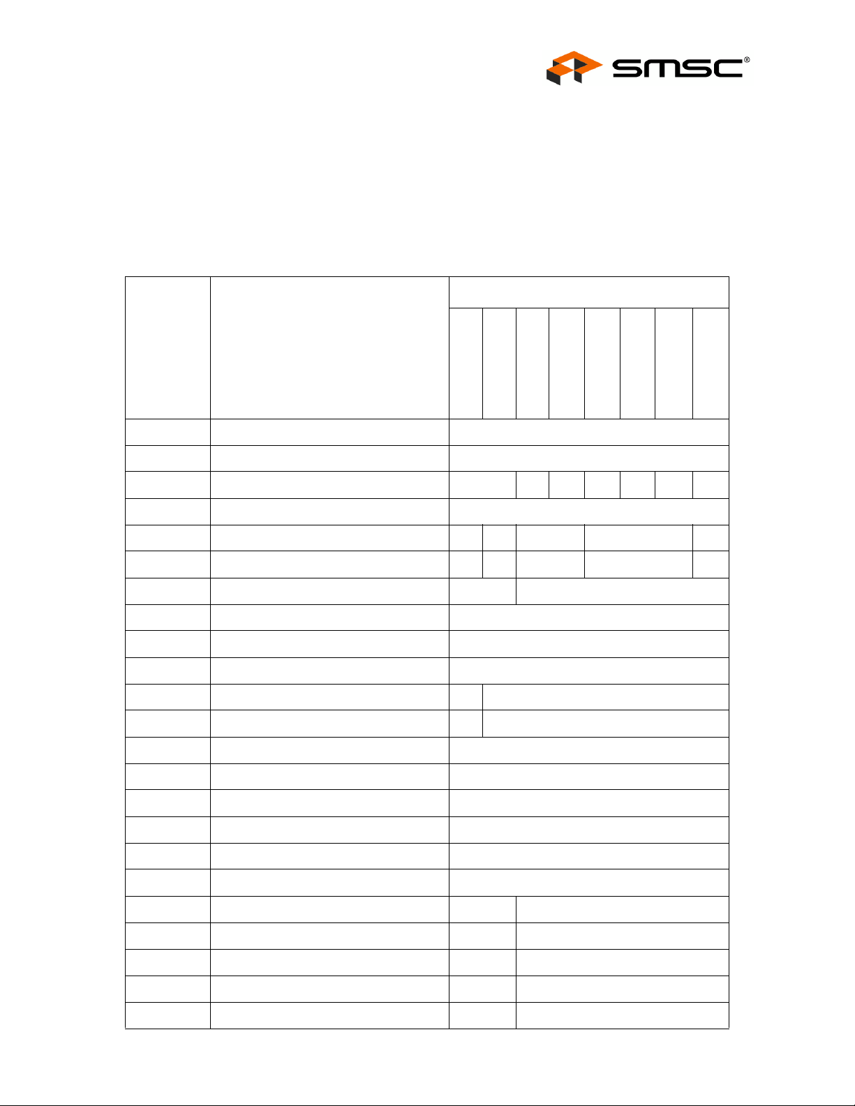
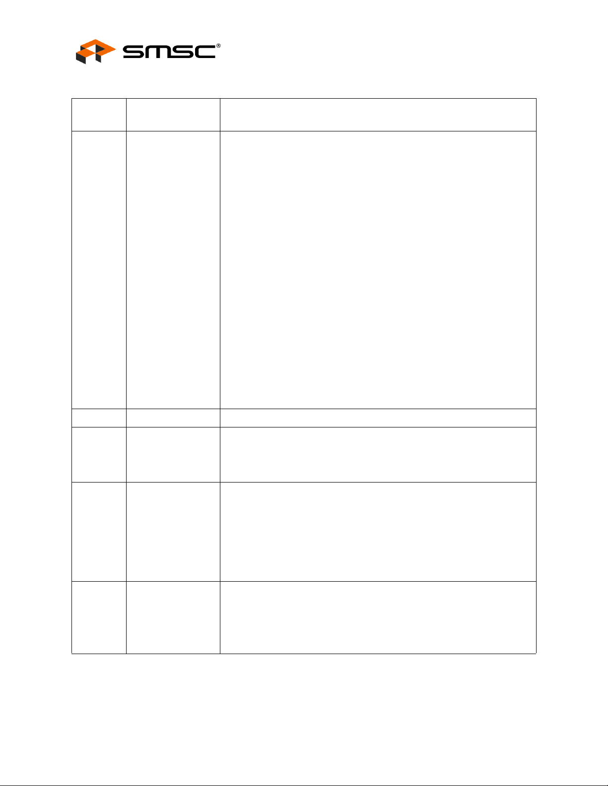
Chapter 4 Block Diagram
To Upstream
V
BUS
Upstream
USB Data
3.3 V
24 MHz
Crystal
To EEPROM or
SMBus Master
SCK
SDA
3.3 V
Bus-
Power
Detect/
Pulse
V
bus
Regulator
CRFILT
Upstream
Regulator
PHY
Serial
Repeater
Interface
Engine
TT
#1
Routing & Port Re-Ordering Logic
Port #1
PHY#1
OC Sense
Switch Driver/
LED Drivers
...
PLL
...
PHY#x
Serial
Interface
Controller
TT
Controller
#x
Port #x
OC Sense
Switch Driver/
LED Drivers
Port
USB Data
Downstream
OC
Sense
Switch/
LED
Drivers
Port
Power
USB Data
Downstream
OC
Sense
Switch/
LED
Drivers
Port
Power
The ‘x’ indicates the number of available downstream ports: 2, 3, 4, or 7.
Figure 4.1 USB251x Hub Family Block Diagram
Note 4.1 USB2512A/USB2512Ai only supports a single transaction translator.
Note 4.2 The LED port indicators only apply to USB2513/14 (48QFN only) and USB2517/17i.
SMSC USB251x 11 Revision 1.0 (3-11-09)
DATASHEET
Page 12
USB 2.0 Hi-Speed Hub Controller
Datasheet
Chapter 5 Pin Descriptions
This chapter is organized by a set of pin configurations (organized by package type) followed by a
corresponding pin list organized alphabetically. A comprehensive and detailed description list of each
signal (named in the pin list) is organized by function in Table 5.2, “USB251x Pin Descriptions,” on
page 22. Please refer to Table 5.3, “Buffer Type Descriptions,” on page 27 for a list of buffer types.
The “N” symbol in the signal name indicates that the active, or asserted, state occurs when the signal
is at a low voltage level. When “N” is not present after the signal name, the signal is asserted when it
is at the high voltage level. The terms assertion and negation are used exclusively. This is done to
avoid confusion when working with a mixture of “active low” and “active high” signals. The term assert,
or assertion, indicates that a signal is active, independent of whether that level is represented by a
high or low voltage. The term negate, or negation, indicates that a signal is inactive.
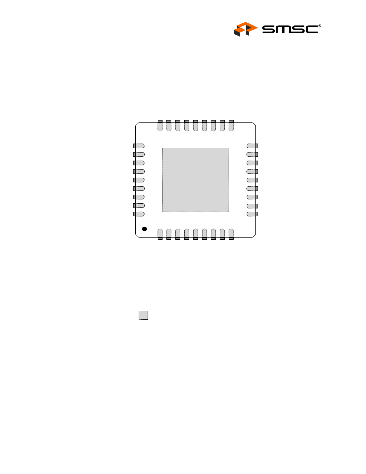
5.1 Pin Configurations and Lists (Organized by Package Type)
SUSP_IND / LOCAL_PWR / NON_REM[0]
VDD33
USBDM_UP
USBDP_UP
XTALOUT
XTALIN / CLKIN
PLLFILT
RBIAS
VDD33
RESET_N24HS_IND / CFG_SEL[1]23SCL / SMBCLK / CFG_SEL[0]
VBUS_DET
26
27
28
29
30
31
USB2512/12A/12B
32
USB2512i/12Ai/12Bi
33
(Top View QFN-36)
34
35
(must be connected to VSS)
36
1
2
USBDP_DN[1]
USBDM_DN[1]
VDD33
25
SMSC
Ground Pad
3
4
5NC6NC7NC8NC9
VDD33
USBDP_DN[2]
USBDM_DN[2]
SDA / SMBDATA / NON_REM[1]21NC20NC
22
NC
19
18
17
16
15
14
13
12
11
10
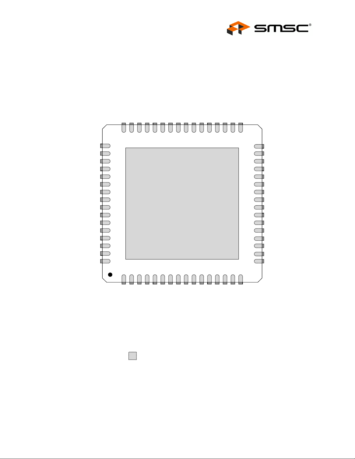
Indicates pins on the bottom of the device.
NC
OCS_N[2]
PRTPWR[2] / BC_EN[2]*
VDD33
CRFILT
OCS_N[1]
PRTPWR[1] / BC_EN[1]*
TEST
VDD33
Figure 5.1 2-Port 36-Pin QFN
Note: *Battery charging enable (BC_EN) is only available in the USB251xB/Bi.
Revision 1.0 (3-11-09) 12 SMSC USB251x
DATASHEET
Page 13
USB 2.0 Hi-Speed Hub Controller
Datasheet
SUSP_IND / LOCAL_PWR / NON_REM[0]
VDD33
USBDM_UP
USBDP_UP
XTALOUT
XTALIN / CLKIN
PLLFILT
RBIAS
VDD33
RESET_N24HS_IND / CFG_SEL[1]23SCL / SMBCLK / CFG_SEL[0]
VBUS_DET
26
27
25
28
29
30
31
32
33
(Top View QFN-36)
34
35
(must be connected to VSS)
SMSC
USB2513/13i
USB2513B/13Bi
Ground Pad
36
1
2
3
4
VDD33
SDA / SMBDATA / NON_REM[1]21NC20NC
22
5
6
VDD33
7NC8NC9
OCS_N[3]
19
18
17
16
15
14
13
12
11
10
PRTPW R[3] / BC_EN[3]*
OCS_N[2]
PRTPW R[2] / BC_EN[2]*
VDD33
CRFILT
OCS_N[1]
PRTPW R[1] / BC_EN[1]*
TEST
VDD33
USBDP_DN[1] / PRT_DIS_P[1]
USBDM_DN[1] / PRT_DIS_M[1]
USBDM_DN[2] / PRT_DIS_M[2]
USBDP_DN[2] / PRT_DIS_P[2]
USBDM_DN[3] / PRT_DIS_M[3]
USBDP_DN[3] / PRT_DIS_P[3]
Indicates pins on the bottom of the device.
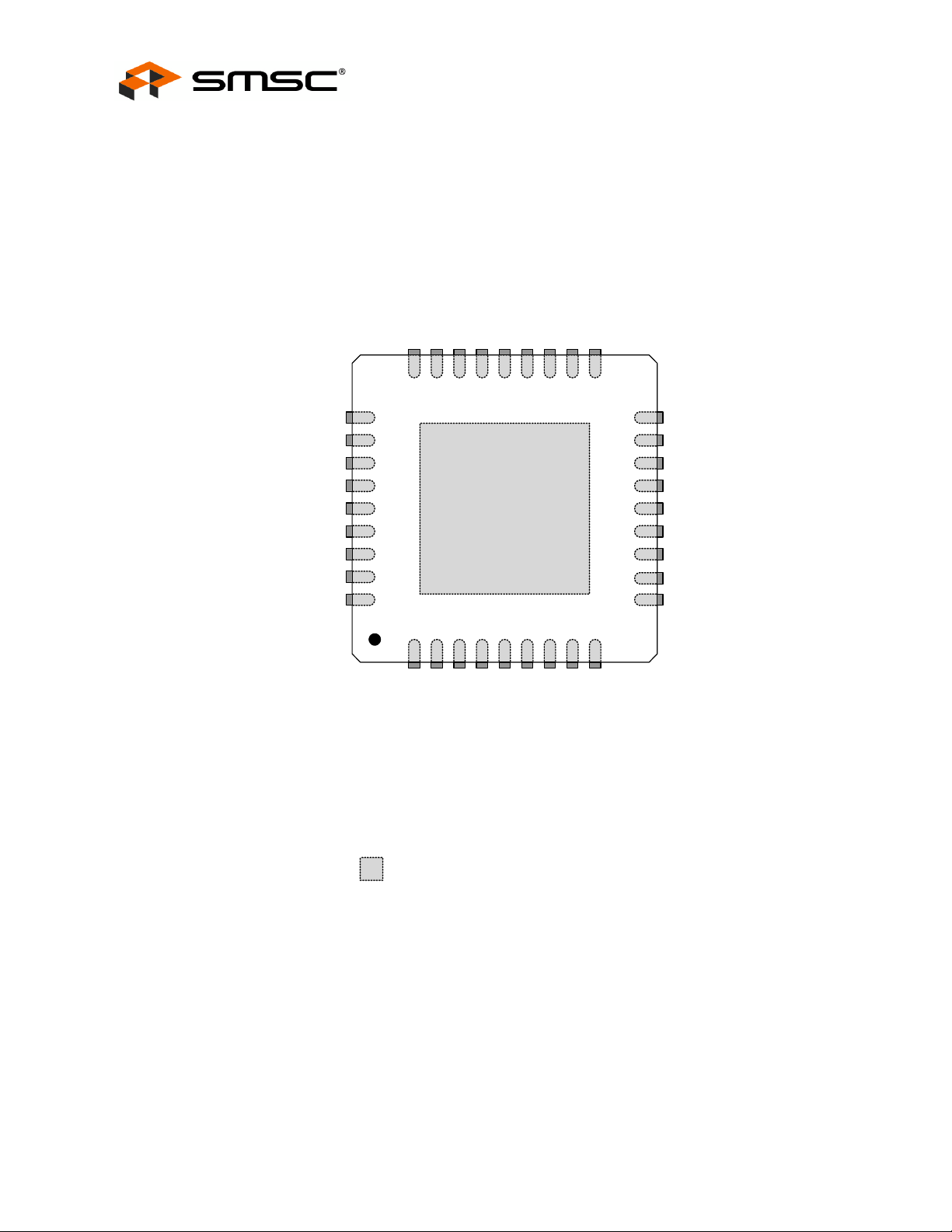
Figure 5.2 3-Port 36-pin QFN
Note: *Battery charging enable (BC_EN) is only available in the USB251xB/Bi.
SMSC USB251x 13 Revision 1.0 (3-11-09)
DATASHEET
Page 14
USB 2.0 Hi-Speed Hub Controller
Datasheet
SUSP_IND / LOCAL_PWR / NON_REM[0]
VDD33
USBDM_UP
USBDP_UP
XTALOUT
XTALIN / CLKIN
PLLFILT
RBIAS
VDD33
RESET_N24HS_IND / CFG_SEL[1]23SCL / SMBCLK / CFG_SEL[0]
VBUS_DET
26
25
27
28
29
30
31
32
33
(Top View QFN-36)
34
35
(must be connected to VSS)
SMSC
USB2514/14i
USB2514B/14Bi
Ground Pad
36
1
2
3
4
VDD33
5
VDD33
SDA / SMBDATA / NON_REM[1]21OCS_N[4]20PRTPWR[4] / BC_EN[4]*
22
6
7
OCS_N[3]
19
18
17
16
15
14
13
12
11
10
8
9
PRTPWR[3] / BC_EN[3]*
OCS_N[2]
PRTPWR[2] / BC_EN[2]*
VDD33
CRFILT
OCS_N[1]
PRTPWR[1] / BC_EN[1]*
TEST
VDD33
USBDP_DN[1] / PRT_DIS_P[1]
USBDM_DN[1] / PRT_DIS_M[1]
USBDM_DN[2] / PRT_DIS_M[2]
USBDP_DN[2] / PRT_DIS_P[2]
USBDM_DN[3] / PRT_DIS_M[3]
USBDP_DN[3] / PRT_DIS_P[3]
USBDM_DN[4] / PRT_DIS_M[4]
USBDP_DN[4] / PRT_DIS_P[4]
Indicates pins on the bottom of the device.
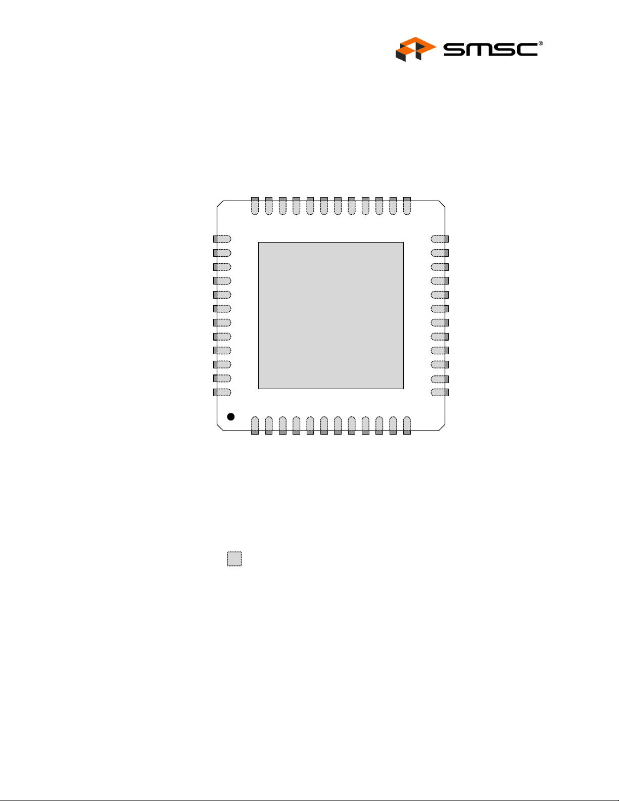
Figure 5.3 4-Port 36-pin QFN
Note: *Battery charging enable (BC_EN) is only available in the USB251xB/Bi.
Revision 1.0 (3-11-09) 14 SMSC USB251x
DATASHEET
Page 15
USB 2.0 Hi-Speed Hub Controller
Datasheet
LED_A_N[1] / PRTSWP[1]
PRTPWR_POL
SUSP_IND / LOCAL_PWR / NON_REM[0]
SEL48
VDD33
USBDM_UP
USBDP_UP
XTALOUT
XTALIN / CLKIN
PLLFILT
RBIAS
VDD33
37
38
39
40
41
42
43
44
45
46
47
48
LED_B_N[1] / BOOST[0]34VBUS_DET33RESET_N
35
36
HS_IND / CFG_SEL[1]31SCL / SMBCLK / CFG_SEL[0]30VDD3329SDA / SMBDATA / NON_REM[1]28NC
CFG_SEL[2]
32
SMSC
USB2513
(Top View QFN-48)
Ground Pad
(must be connected to VSS)
1
2
3
4
5
VDD33
6
7NC8NC9NC10NC11
OCS_N[3]25LED_A_N[2] / PRTSWP[2]
27NC26
VDD33
12
24
23
22
21
20
19
18
17
16
15
14
13
LED_B_N[2] / BOOST[1]
LED_A_N[3] / PRTSWP[3]
LED_B_N[3] / GANG_EN
PRTPWR[3]
OCS_N[2]
PRTPWR[2]
VDD33
CRFILT
OCS_N[1]
PRTPWR[1]
TEST
NC
USBDP_DN[1] / PRT_DIS_P[1]
USBDM_DN[1] / PRT_DIS_M[1]
USBDP_DN[2] / PRT_DIS_P[2]
USBDM_DN[2] / PRT_DIS_M[2]
USBDP_DN[3] / PRT_DIS_P[3]
USBDM_DN[3] / PRT_DIS_M[3]
Indicates pins on the bottom of the device.
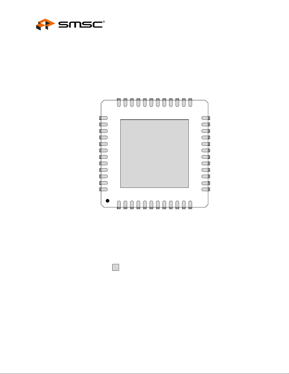
Figure 5.4 3-Port 48-Pin QFN
SMSC USB251x 15 Revision 1.0 (3-11-09)
DATASHEET
Page 16
USB 2.0 Hi-Speed Hub Controller
Datasheet
LED_A_N[1] / PRTSWP[1]
PRTPWR_POL
SUSP_IND / LOCAL_PWR / NON_REM[0]
SEL48
VDD33
USBDM_UP
USBDP_UP
XTALOUT
XTALIN / CLKIN
PLLFILT
RBIAS
VDD33
37
38
39
40
41
42
43
44
45
46
47
48
LED_B_N[1] / BOOST[0]34VBUS_DET33RESET_N
35
36
HS_IND / CFG_SEL[1]31SCL / SMBCLK / CFG_SEL[0]30VDD3329SDA / SMBDATA / NON_REM[1]28OCS_N[4]
CFG_SEL[2]
32
SMSC
USB2514
(Top View QFN-48)
Ground Pad
(must be connected to VSS)
1
2
3
4
5
VDD33
PRTPWR[4]26OCS_N[3]25LED_A_N[2] / PRTSWP[2]
27
24
23
22
21
20
19
18
17
16
15
14
13
6
7
8
9
10NC11
12
VDD33
LED_B_N[4]
LED_B_N[2] / BOOST[1]
LED_A_N[3] / PRTSWP[3]
LED_B_N[3] / GANG_EN
PRTPWR[3]
OCS_N[2]
PRTPWR[2]
VDD33
CRFILT
OCS_N[1]
PRTPWR[1]
TEST
LED_A_N[4] / PRTSWP[4]
USBDP_DN[1] / PRT_DIS_P[1]
USBDM_DN[1] / PRT_DIS_M[1]
USBDP_DN[2] / PRT_DIS_P[2]
USBDM_DN[2] / PRT_DIS_M[2]
USBDP_DN[3] / PRT_DIS_P[3]
USBDM_DN[3] / PRT_DIS_M[3]
USBDP_DN[4] / PRT_DIS_P[4]
USBDM_DN[4] / PRT_DIS_M[4]
Indicates pins on the bottom of the device.
Figure 5.5 4-Port 48-Pin QFN
Revision 1.0 (3-11-09) 16 SMSC USB251x
DATASHEET
Page 17
USB 2.0 Hi-Speed Hub Controller
Datasheet
LED_A_N[2] / PRTSWP[2]
LED_B_N[1] / BOOST[0]
LED_A_N[1] / PRTSWP[1]
VDD33
USBDM_DN[6] / PRT_DIS_M[6]
USBDP_DN[6] / PRT_DIS_P[6]
USBDM_DN[7] / PRT_DIS_M[7]
USBDP_DN[7] / PRT_DIS_P[7]
VDD33
USBDM_UP
USBDP_UP
XTALOUT
XTALIN / CLKIN
PLLFILT
RBIAS
VDD33
49
50
51
52
53
54
55
56
57
58
59
60
61
62
63
64
VDD3344SUSP_IND / LOCAL_PWR / NON_REM[0]43VBUS_DET42HS_IND / CFG_SEL[1]41SCL / SMBCLK / CFG_SEL[0]40SDA / SMBDATA / NON_REM[1]39PRTPWR[6]38OCS_N[6]
LED_B_N[2] / BOOST[1]
LED_A_N[3] / PRTSWP[3]
46
47
48
RESET_N
45
USB2517/17i
(Top View QFN-64)
(must be connected to VSS)
1
2
3
4
5
6
SMSC
Ground Pad
7
8
9
10
11
OCS_N[7]36PRTPWR[7]35OCS_N[5]
37
12
13
14
LED_B_N[3] / GANG_EN
34
15
LED_A_N[4] / PRTSWP[4]
33
16
32
31
30
29
28
27
26
25
24
23
22
21
20
19
18
17
LED_B_N[4]
LED_A_N[5] / PRTSWP[5]
PRTPWR[5]
PRTPWR[1]
OCS_N[1]
OCS_N[2]
PRTPWR[2]
CRFILT
VDD33
PRTPWR[3]
OCS_N[3]
OCS_N[4]
PRTPWR[4]
TEST
LED_B_N[5]
LED_A_N[6] / PRTSWP[6]
VDD33
USBDP_DN[1] / PRT_DIS_P[1]
USBDM_DN[1] / PRT_DIS_M[1]
USBDP_DN[2] / PRT_DIS_P[2]
USBDM_DN[2] / PRT_DIS_M[2]
USBDP_DN[3] / PRT_DIS_P[3]
USBDM_DN[3] / PRT_DIS_M[3]
VDD33
LED_B_N[6]
LED_B_N[7]
CFG_SEL[2]
LED_A_N[7] / PRTSWP[7]
USBDP_DN[4] / PRT_DIS_P[4]
USBDM_DN[4] / PRT_DIS_M[4]
USBDP_DN[5] / PRT_DIS_P[5]
USBDM_DN[5] / PRT_DIS_M[5]
Indicates pins on the bottom of the device.
Figure 5.6 7-Port 64-Pin QFN
SMSC USB251x 17 Revision 1.0 (3-11-09)
DATASHEET
Page 18
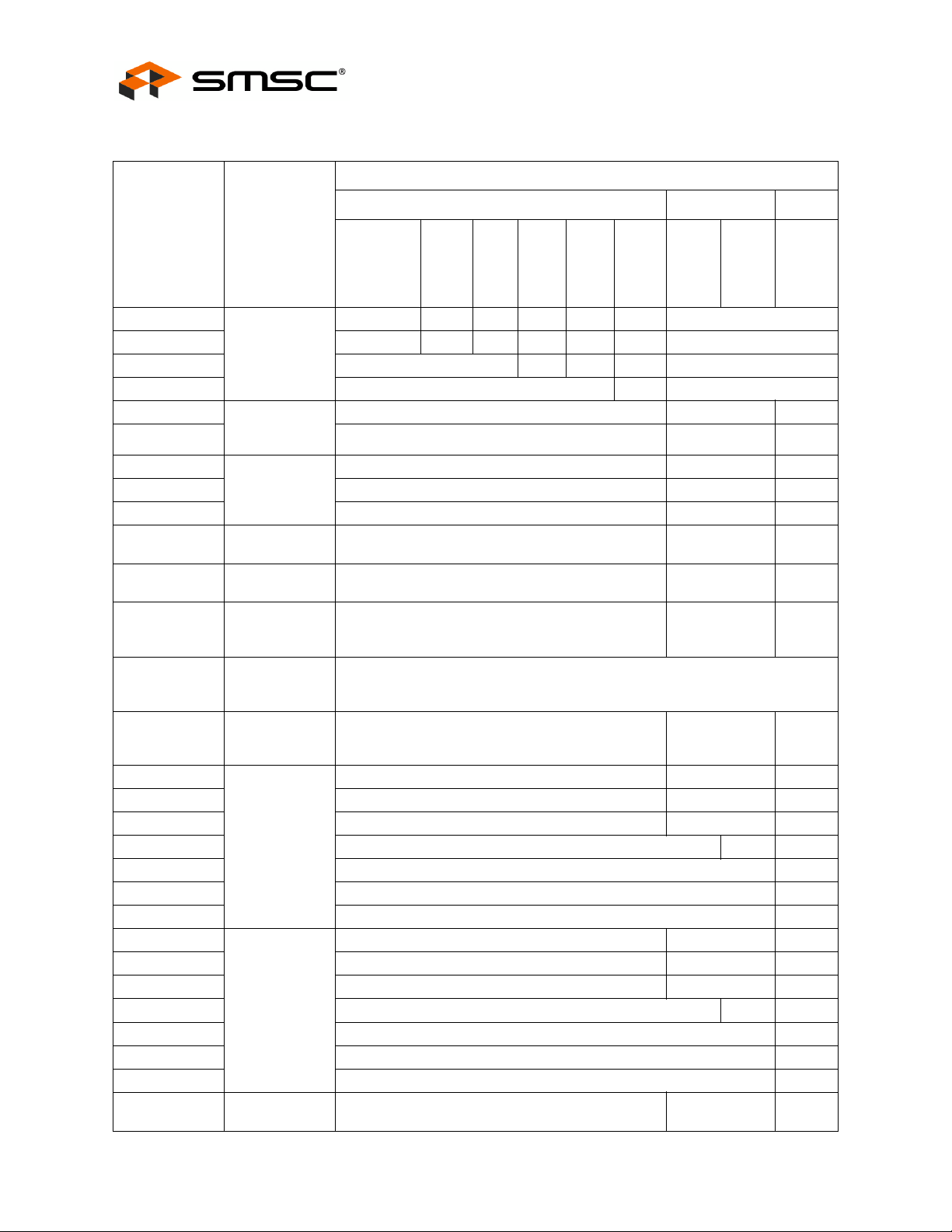
Table 5.1 Pin List in Alphabetical Order
PIN NUMBERS
36 QFN 48QFN 64 QFN
USB 2.0 Hi-Speed Hub Controller
Datasheet
SYMBOL NAME
BC_EN[1] Battery
BC_EN[2] - 16 - 16 - 16 -
Charging Strap
Option
USB2512
USB2512i
USB2512A
USB2512Ai
USB2512B
USB2512Bi
USB2513
USB2513i
USB2513B
USB2513Bi
USB2514
USB2514i
USB2514B
USB2514Bi
USB2513
USB2514
-12-12-12 -
BC_EN[3] - 18 - 18 -
BC_EN[4] - 20 -
BOOST[0] PHY Boost
BOOST[1] - 24 48
Strapping
Option
CFG_SEL[0] Configuration
CFG_SEL[1] 25 32 42
Programming
Selection
-3650
24 31 41
CFG_SEL[2] - 33 13
CLKIN External Clock
33 45 61
Input
CRFILT Core Regulator
14 17 25
Filter Capacitor
GANG_EN Ganged Port
-2234
Power Strap
Option
Ground Pad Exposed Pad
ePad
Tied to Ground
(VSS)
HS_IND Hi-Speed
25 32 42
Upstream Port
Indicator
LED_A_N[1] Port LED
LED_A_N[2] - 25 49
Indicator
-3751
LED_A_N[3] - 23 47
LED_A_N[4] - 13 33
LED_A_N[5] - 31
LED_A_N[6] - 17
LED_A_N[7] - 15
LED_B_N[1] Enhanced
LED_B_N[2] - 24 48
Indicator
Port LED
-3650
LED_B_N[3] - 22 34
LED_B_N[4] - 12 32
LED_B_N[5] - 18
LED_B_N[6] - 16
LED_B_N[7] - 14
LOCAL_PWR Local Power
28 39 45
Detection
USB2517
USB2517i
Revision 1.0 (3-11-09) 18 SMSC USB251x
DATASHEET
Page 19
USB 2.0 Hi-Speed Hub Controller
Datasheet
Table 5.1 Pin List in Alphabetical Order (continued)
PIN NUMBERS
36 QFN 48QFN 64 QFN
SYMBOL NAME
USB2512
USB2512i
USB2512A
USB2512Ai
USB2512B
USB2512Bi
USB2513
USB2513i
USB2513B
USB2513Bi
USB2514
USB2514i
USB2514B
USB2514Bi
USB2513
USB2514
NC No Connect 6 - 8 11 -
NC 7 - 9 -
NC 18 - 11 -
NC 19 - 12 -
NC 8 - 13 -
NC 9 - 27 -
NC 20 - 28 -
NC 21 -
NON_REM[0] Non-
NON_REM[1] 22 29 40
Removable
Port Strap
28 39 45
Option
OCS_N[1] Over-Current
OCS_N[2] 17 20 27
Sense
13 16 28
OCS_N[3] - 19 26 22
OCS_N[4] - 21 - 28 21
OCS_N[5] - 35
OCS_N[6] - 38
OCS_N[7] - 37
PLLFILT PLL Regulator
34 46 62
Filter Capacitor
PRT_DIS_M[1] Downstream
PRT_DIS_M[2] - 3
Port Disable
Strap Option
-1
PRT_DIS_M[3] - 6
PRT_DIS_M[4] - 8 - 8
PRT_DIS_M[5] - 11
PRT_DIS_M[6] - 53
PRT_DIS_M[7] - 55
PRT_DIS_P[1] Port Disable - 2
PRT_DIS_P[2] - 4
PRT_DIS_P[3] - 7
PRT_DIS_P[4] - 9 - 9
PRT_DIS_P[5] - 12
PRT_DIS_P[6] - 54
PRT_DIS_P[7] - 56
USB2517
USB2517i
SMSC USB251x 19 Revision 1.0 (3-11-09)
DATASHEET
Page 20
Table 5.1 Pin List in Alphabetical Order (continued)
PIN NUMBERS
36 QFN 48QFN 64 QFN
USB 2.0 Hi-Speed Hub Controller
Datasheet
SYMBOL NAME
PRTPWR[1] USB Port
PRTPWR[2] 16 19 26
Power Enable
USB2512
USB2512i
USB2512A
USB2512Ai
USB2512B
USB2512Bi
USB2513
USB2513i
USB2513B
USB2513Bi
USB2514
USB2514i
USB2514B
USB2514Bi
USB2513
USB2514
12 15 29
PRTPWR[3] - 18 21 23
PRTPWR[4] - 20 - 27 20
PRTPWR[5] - 30
PRTPWR[6] - 39
PRTPWR[7] - 36
PRTPWR_POL Port Power
-38-
Polarity
Strapping
PRTSWP[1] Port Swap
PRTSWP[2] - 25 49
Strapping
Option
-3751
PRTSWP[3] - 23 47
PRTSWP[4] - 13 33
PRTSWP[5] - 31
PRTSWP[6] - 17
PRTSWP[7] - 15
RBIAS USB
35 47 63
Transceiver
Bias
RESET_N Reset Input 26 34 43
SCL Serial Clock 24 31 41
SDA Serial Data
22 29 40
Signal
SEL48
Clock Input
SMBCLK System
Select 48 MHz
-40-
24 31 41
Management
Bus Clock
SMBDATA Server
22 29 40
Message Block
Data Signal
SUSP_IND Active/Suspend
28 39 45
Status Indicator
TEST Test Pin 11 14 19
USBDM_UP USB Bus Data 30 42 58
USBDP_UP 31 43 59
USB2517
USB2517i
Revision 1.0 (3-11-09) 20 SMSC USB251x
DATASHEET
Page 21
USB 2.0 Hi-Speed Hub Controller
Datasheet
Table 5.1 Pin List in Alphabetical Order (continued)
PIN NUMBERS
36 QFN 48QFN 64 QFN
SYMBOL NAME
USBDM_DN[1] Hi-Speed USB
USBDM_DN[2] 3
Data
USB2512
USB2512i
USB2512A
USB2512Ai
USB2512B
USB2512Bi
USB2513
USB2513i
USB2513B
USB2513Bi
USB2514
USB2514i
USB2514B
USB2514Bi
USB2513
USB2514
1
USBDM_DN[3] - 6
USBDM_DN[4] - 8 - 8
USBDM_DN[5] - 11
USBDM_DN[6] - 53
USBDM_DN[7] - 55
USBDP_DN[1] 2
USBDP_DN[2] 4
USBDP_DN[3] - 7
USBDP_DN[4] - 9 - 9
USBDP_DN[5] - 12
USBDP_DN[6] - 54
USBDP_DN[7] - 56
VBUS_DET Upstream
27 35 44
VBUS Power
Detection
VDD33 3.3 V Power 5
VDD33 10
VDD33 15 18 24
VDD33 23 30 46
VDD33 29 41 52
VDD33 36 48 57
VDD33 - 64
XTALIN Crystal Input 33 45 61
XTALOUT Crystal Output 32 44 60
USB2517
USB2517i
SMSC USB251x 21 Revision 1.0 (3-11-09)
DATASHEET
Page 22
USB 2.0 Hi-Speed Hub Controller
5.2 USB251x Pin Descriptions (Grouped by Function)
Table 5.2 USB251x Pin Descriptions
BUFFER
SYMBOL
TYPE DESCRIPTION
UPSTREAM USB 2.0 INTERFACES
Datasheet
USBDM_UP
USBDP_UP
VBUS_DET I/O12 Detect Upstream VBUS Power
USBDP_DN[x:1]/
PRT_DIS_P[x:1]
USBDM_DN[x:1]/
PRT_DIS_M[x:1]
IO-U USB Data
These pins connect to the upstream USB bus data signals (host, port, or
upstream hub).
Detects state of Upstream VBUS power. The SMSC hub monitors
VBUS_DET to determine when to assert the internal D+ pull-up resistor which
signals a connect event.
When designing a detachable hub, this pin should be connected to VBUS on
the upstream port via a 2 to 1 voltage divider.
For self-powered applications with a permanently attached host, this pin must
be connected to 3.3 V (typically VDD33).
DOWNSTREAM USB 2.0 INTERFACES
IO-U Hi-Speed USB Data
These pins connect to the downstream USB peripheral devices attached to
the hub’s port. To disable, pull up with a 10 K resistor to 3.3 V.
Downstream Port Disable Strap Option
If this strap is enabled by package and configuration settings (see Table 8.1,
"Hub Configuration Options"), then this pin will be sampled at RESET_N
negation to determine if the port is disabled.
To disable a port, pull up both PRT_DIS_M[x:1] and PRT_DIS_P[x:1] pins
corresponding to the port numbers.
PRTPWR[x:1] /
BC_EN[x]
Revision 1.0 (3-11-09) 22 SMSC USB251x
O12 USB Power Enable
Enables power to USB peripheral devices downstream.
When PRTPWR_POL pin is unavailable, the hub supports active high power
controllers only.
When PRTPWR_POL pin is available, the active signal level of the PRTPWR
pins is determined by the power polarity strapping function of the
PRTPWR_POL pin.
IPD Battery Charging Strap Option
*This feature is only available on USB251xB/Bi.
If this strap is enabled by package and configuration settings, (see Table 8.1,
"Hub Configuration Options"), this pin will be sampled at RESET_N negation
to determine if ports [x:1] support the battery charging protocol (and thus the
supporting external port power controllers) that would enable a device to draw
the currents per the USB battery charging specification.
BC_EN[x] = 1: Battery charging feature is supported for port x
BC_EN[x] = 0: Battery charging feature is not supported for
port x
DATASHEET
Page 23
USB 2.0 Hi-Speed Hub Controller
Datasheet
BUFFER
SYMBOL
TYPE DESCRIPTION
Table 5.2 USB251x Pin Descriptions (continued)
DOWNSTREAM USB 2.0 INTERFACES (continued)
LED_A_N[x:1] /
I/O12 Port LED Indicators
This pin will be active low when LED support is enabled via EEPROM or
SMBus.
PRTSWP[x:1]
Port Swap Strapping Option
If this strap is enabled by package and configuration settings (see Table 8.1,
"Hub Configuration Options"), this pin will be sampled at RESET_N negation
to determine the electrical connection polarity of the downstream USB port
pins (USB_DP and USB_DM).
Also, the active state of the LED will be determined as follows:
‘0’ = Port polarity is normal, LED is active high.
‘1’ = Port polarity (USB_DP and USB_DM) is swapped, LED is active low.
LED_B_N[7:4] I/O12 Enhanced Indicator Port LED for ports 4-7
Enhanced indicator LED for ports 4-7. This pin will be active low when LED
support is enabled via EEPROM or SMBus.
LED_B_N[3] /
GANG_EN
I/O12 Enhanced Indicator Port LED for Port 3
Ganged Power and Over-current strap option
This signal selects between ganged or individual port power and over-current
sensing. If this strap is enabled by package and configuration settings (see
Table 8.1, "Hub Configuration Options"), this pin will be sampled at RESET_N
negation to determine the mode as follows:
‘0’ = Individual sensing and switching, LED_B_N[3] is active high.
‘1’ = Ganged sensing and switching, LED_B_N[3] is active low.
SMSC USB251x 23 Revision 1.0 (3-11-09)
DATASHEET
Page 24
SYMBOL
USB 2.0 Hi-Speed Hub Controller
Datasheet
Table 5.2 USB251x Pin Descriptions (continued)
BUFFER
TYPE DESCRIPTION
DOWNSTREAM USB 2.0 INTERFACES (continued)
LED_B_N[2:1] /
I/O12 Enhanced Indicator Port LED for ports 1 and 2
Enhanced indicator LED for ports 1 and 2. This pin will be active low when
LED support is enabled via EEPROM or SMBus.
BOOST[1:0]
If this strap option is enabled by package and configuration settings (see
Table 8.1, "Hub Configuration Options"), this pin will be sampled at RESET_N
negation to determine if all PHY ports (upstream and downstream) operate at
a normal or boosted electrical level. Also, the active state of the LEDs will be
determined as follows:
See Section 8.2.1.27, "Register F6h: Boost_Up," on page 45 and Section
8.2.1.29, "Register F8h: Boost_4:0," on page 47 for more information.
BOOST[1:0] = BOOST_IOUT[1:0]
BOOST[1:0] = ‘00’,
LED_B_N[2] is active high,
LED_B_N[1] is active high.
BOOST[1:0] = ‘01’,
LED_B_N[2] is active high,
LED_B_N[1] is active low.
BOOST[1:0] = ‘10’,
LED_B_N[2] is active low,
LED_B_N[1] is active high.
BOOST[1:0] = ‘11’,
LED_B_N[2] is active low,
LED_B_N[1] is active low.
PRTPWR_POL IPU Port Power Polarity Strapping
Port Power Polarity strapping determination for the active signal polarity of
the [x:1]PRTPWR pins.
While RESET_N is asserted, the logic state of this pin will (through the use
of internal combinatorial logic) determine the active state of the PRTPWR
pins in order to ensure that downstream port power is not inadvertently
enabled to inactive ports during a hardware reset.
When RESET_N is negated, the logic value will be latched internally, and will
retain the active signal polarity for the PRTPWR[x:1] pins.
‘1’ = PRTPWR[x:1]_P/N pins have an active ‘high’ polarity
‘0’ = PRTPWR[x:1]_P/N pins have an active ‘low’ polarity
Warning: Active low port power controllers may glitch the downstream port
power when the system power is first applied. Care should be taken when
designing with active low components.
When PRTPWR_POL is not an available pin on the package, the hub will only
support active high power controllers.
OCS_N[x:1] IPU Over-Current Sense
Input from external current monitor indicating an over-current condition.
RBIAS I-R USB Transceiver Bias
A 12.0 k
Ω (+/- 1%) resistor is attached from ground to this pin to set the
transceiver’s internal bias settings.
Revision 1.0 (3-11-09) 24 SMSC USB251x
DATASHEET
Page 25
USB 2.0 Hi-Speed Hub Controller
Datasheet
BUFFER
SYMBOL
TYPE DESCRIPTION
Table 5.2 USB251x Pin Descriptions (continued)
SERIAL PORT INTERFACES
SDA /
SMBDATA /
NON_REM[1]
I/OSD12 Serial Data signal (SDA)
Server Message Block Data signal (SMBDATA)
Non-removable port strap option
If this strap is enabled by package and configuration settings (see Ta bl e 8 .1 ),
this pin will be sampled (in conjunction with LOCAL_PWR / SUSP_IND /
NON_REM[0]) at RESET_N negation to determine if ports [7:1] contain
permanently attached (non-removable) devices:
NON_REM[1:0] = ‘00’, All ports are removable.
NON_REM[1:0] = ‘01’, Port 1 is non-removable.
NON_REM[1:0] = ‘10’, Ports 1 & 2 are non-removable.
NON_REM[1:0] = ‘11’, When available, ports 1 2 & 3 are non-removable.
RESET_N IS RESET Input
The system can reset the chip by driving this input low. The minimum active
low pulse is 1 μs.
SCL /
SMBCLK /
CFG_SEL[0]
I/OSD12 Serial Clock (SCL)
System Management Bus Clock (SMBCLK)
Configuration Select: The logic state of this multifunction pin is internally
latched on the rising edge of RESET_N (RESET_N negation), and will
determine the hub configuration method as described in Table 8.1, "Hub
Configuration Options".
HS_IND /
I/O12 Hi-Speed Upstream Port Indicator
HS_IND: Hi-speed Indicator for upstream port connection speed.
The active state of the LED will be determined as follows:
CFG_SEL[1] = ‘0’,
HS_IND is active high,
CFG_SEL[1] = ‘1’,
HS_IND is active low,
‘Asserted’ = the hub is connected at HS
‘Negated’ = the hub is connected at FS
CFG_SEL[1]
Configuration Programming Select
CFG_SEL[1]: The logic state of this pin is internally latched on the rising edge
of RESET_N (RESET_N negation), and will determine the hub configuration
method as described in Table 8.1, "Hub Configuration Options".
CFG_SEL[2] I Configuration Programming Select
The logic state of this pin is internally latched on the rising edge of RESET_N
(RESET_N negation), and will determine the hub configuration method as
described in Table 8.1, "Hub Configuration Options". When the CFG_SEL[2]
pin is unavailable, then the logic is internally tied to ‘0’.
SMSC USB251x 25 Revision 1.0 (3-11-09)
DATASHEET
Page 26

Table 5.2 USB251x Pin Descriptions (continued)
BUFFER
SYMBOL
TYPE DESCRIPTION
XTALIN ICLKx Crystal Input
24 MHz crystal
This pin connects to either one terminal of the crystal or to an external
24 MHz clock when a crystal is not used.
CLKIN External Clock Input
This pin connects to either one terminal of the crystal or to an external
24 MHz clock when a crystal is not used.
XTALOUT OCLKx Crystal Output
24 MHz Crystal
This is the other terminal of the crystal, or a no connect pin, when an external
clock source is used to drive XTALIN/CLKIN.
USB 2.0 Hi-Speed Hub Controller
Datasheet
MISC
SUSP_IND /
LOCAL_PWR /
NON_REM[0]
I/O Active/Suspend status LED
Suspend Indicator: Indicates USB state of the hub.
‘negated’ = Unconfigured, or configured and in USB Suspend
‘asserted’ = the hub is configured, and is active (i.e., not in suspend)
Local Power: Detects availability of local self-power source.
Low = Self/local power source is NOT available (i.e., the hub gets all power
from Upstream USB VBus).
High = Self/local power source is available.
NON_REM[0] Strap Option:
If this strap is enabled by package and configuration settings (see Table 8.1,
"Hub Configuration Options"), this pin will be sampled (in conjunction with
NON_REM[1]) at RESET_N negation to determine if ports [x:1] contain
permanently attached (non-removable) devices. Also, the active state of the
LED will be determined as follows:
NON_REM[1:0] = ‘00’, All ports are removable, and the LED is active high
NON_REM[1:0] = ‘01’, Port 1 is non-removable, and the LED is active low
NON_REM[1:0] = ‘10’, Ports 1 & 2 are non-removable, and the LED is active
high
NON_REM[1:0] = ‘11’, When available, ports 1, 2 & 3 are non-removable, and
the LED is active low
TEST IPD TEST pin
User must treat as a no connect pin or connect to ground. No trace or signal
should be routed or attached to this pin.
Revision 1.0 (3-11-09) 26 SMSC USB251x
DATASHEET
Page 27

USB 2.0 Hi-Speed Hub Controller
Datasheet
Table 5.2 USB251x Pin Descriptions (continued)
BUFFER
SYMBOL
SEL48 I 48 MHz Clock Input Selection
CRFILT VDD Core Regulator Filter Capacitor
VDD33 3.3 V Power
PLLFILT PLL Regulator Filter Capacitor
TYPE DESCRIPTION
48 MHz external input clock select. When the hub is clocked from an external
clock source, this pin selects either 24 MHz or 48 MHz mode.
‘0’ = 24 MHz
‘1’ = 48 MHz
POWER, GROUND, and NO CONNECTS
This pin must have a 1.0 μF (or greater) ±20% (ESR <0.1 Ω) capacitor to
VSS.
This pin must have a 1.0 μF (or greater) ±20% (ESR <0.1
VSS.
VSS Ground Pad / ePad
The package slug is the only VSS for the device and must be tied to ground
with multiple vias.
NC No Connect
No signal or trace should be routed or attached to these pins.
5.3 Buffer Type Descriptions
Table 5.3 Buffer Type Descriptions
BUFFER DESCRIPTION
I Input.
I/O Input/Output.
IPD Input with internal weak pull-down resistor.
IPU Input with internal weak pull-up resistor.
Ω) capacitor to
IS Input with Schmitt trigger.
O12 Output 12 mA.
SMSC USB251x 27 Revision 1.0 (3-11-09)
DATASHEET
Page 28

Table 5.3 Buf fe r Ty p e Descriptions (continued)
BUFFER DESCRIPTION
I/O12 Input/Output buffer with 12 mA sink and 12 mA source.
USB 2.0 Hi-Speed Hub Controller
Datasheet
I/OSD12
Open drain with Schmitt trigger and 12 mA sink. Meets the I
version 2.1, requirements.
ICLKx XTAL clock input.
OCLKx XTAL clock output.
I-R RBIAS.
I/O-U Analog Input/Output defined in USB specification.
2
C-Bus specification,
Revision 1.0 (3-11-09) 28 SMSC USB251x
DATASHEET
Page 29

USB 2.0 Hi-Speed Hub Controller
Datasheet
Chapter 6 LED Usage Description
6.1 LED Functionality
USB2513 and USB2514 (48-pin QFN only) and USB2517/17i SMSC hubs support two different
(mutually exclusive) LED modes. The ‘x’ represents the number of downstream ports. The USB mode
provides up to 14 LED’s that conform to the USB 2.0 specification functional requirements for Green
and Amber LED’s. The LED mode “speed indicator” provides the downstream device connection
speed.
6.1.1 USB Mode 14-Wire
The LED_A_N[x:1] pins are used to provide Green LED support as defined in the USB 2.0
specification. The LED_B_N[x:1] pins are used to provide Amber LED support as defined in the USB
2.0 specification. The USB specification defines the LED’s as port status indicators for the downstream
ports. Please note that no indication of port speed is possible in this mode. The pins are utilized as
follows:
LED_A_N[x:1] = Port [x:1] green LED
LED_B_N[x:1] = Port [x:1] amber LED
6.1.2 LED Mode Speed Indication
The LED_A[x:1]_N pins are used to provide connection status as well as port speed by using dual
color LED's. This scheme requires that the LED's be in the same package, and that a third color is
produced so that the user perceives both LED's as being driven "simultaneously".
The LED_A[x:1] pins used in this mode are connected to x number of dual color LED’s (each LED pair
in a single package). These pins indicate the USB speed of each attached downstream device.
Each dual color LED provides two separate colors (commonly Green and Red). If each of these
separate colors are pulsed on and off at a rapid rate, a user will see a third color (in this example,
Orange). Using this method, 4 different "color" states are possible (Green, Red, Orange, and Off).
3.3 V
Hub LED pin
General
Purpose
Diode
Current Limiting
Resistor
Connection to
other Dual Color
Diodes
D1A (Green LED)
D1B (Red LED)
Figure 6.1 Dual Color LED Implementation Example
SMSC USB251x 29 Revision 1.0 (3-11-09)
DATASHEET
Page 30

USB 2.0 Hi-Speed Hub Controller
Datasheet
Figure 6.1 shows a simple example of how this LED circuit will be implemented. The circuit should be
replicated for each of the x LED pins on the SMSC hub. In this circuit, when the LED pin is driven to
a logic low state, the Green LED will light up. When the LED pin is driven to a Logic High state the
Red LED will light up. When a 1 KHz square wave is driven out on the LED pin, the Green and Red
LED's will both alternately light up giving the effect of the color Orange. When nothing is driven out on
the LED pin (i.e. the pin floats to a "tri-state" condition), neither the Green nor Red LED will light up,
this is the "Off" state.
The assignment is as follows:
LED_A_N[x:1] = LED D[x:1] (Downstream Port [x:1])
The usage is as follows:
LED_A_N[x] Driven to Logic Low = LS device attached (Green LED)
LED_A_N[x] Driven to Logic High = FS device attached (Red LED)
LED_A_N[x] Pulsed @ 1 KHz = HS device attached (Orange color by pulsing Red & Green).
LED_A_N[x] is tri-state= No devices are attached, or the hub is in suspend, LED's are off.
Revision 1.0 (3-11-09) 30 SMSC USB251x
DATASHEET
Page 31

USB 2.0 Hi-Speed Hub Controller
Datasheet
Chapter 7 Battery Charging Support
7.1 General Description
The battery charging feature is only available in USB251xB (which represents USB2512B/3B/4B and
USB2512Bi/3Bi/4Bi hub family products). Any one or combination of downstream ports on the
USB251xB hub can be configured to support battery charging.
The SMSC hub provides support for battery charging devices on a per port basis in compliance with
the USB Battery Charging specification, version 1.1. The hub can be configured to individually enable
each downstream port for battery charging support either via pin strapping as illustrated in Figure 7.1
or by setting the corresponding configuration bits via EEPROM or SMBus.
3.3 V 5 V
R
STRAP
USB Port Power
Controller
IN
USB251xB/xBi
Note: R
7.2 USB Battery Charging
A downstream port enabled for battery charging turns on port power as soon as the configuration
process has completed. The hub does not need to be enumerated nor does VBUS_DET need to be
asserted for the port power to be enabled. These conditions allow battery charging in S3, S4 and S5
system power states as well as in the fully operational state. The USB Battery Charging specification
does not interfere with standard USB operation, which allows a device to perform battery charging at
any time.
A port that supports battery charging must be able to support 1.5 amps of current on VBUS. Standard
USB port power controllers typically only allow for 0.8 amps of current before detecting an over-current
condition. Therefore, the 5 volt power supply, port power controller or over-current protection devices
must be chosen to handle the larger current demand compared to standard USB hub designs.
enables battery charging.
STRAP
Figure 7.1 Battery Charging via External Power Supply
OCS_N[x]
EN
VBUSPRTPWR[x]
FLAG
7.2.1 Special Behavior of PRTPWR Pins
The SMSC hub enables VBUS by asserting the port power (PRTPWR) pin as soon as the hardware
configuration process has completed. If the port detects an over-current condition, PRTPWR will be
turned off to protect the circuitry from overloading. If an over-current condition is detected when the
hub is not enumerated, PRTPWR can only be turned on from the host or if RESET_N is toggled. These
SMSC USB251x 31 Revision 1.0 (3-11-09)
DATASHEET
Page 32

behaviors provide battery charging even when the hub is not enumerated and protect the hub from
sustained short circuit conditions. If the short circuit condition persists when the hub is plugged into a
host system the user is notified that a port has an over-current condition. Otherwise the PRTPWR is
turned on by the host system and the port operates normally.
7.3 Battery Charging Configuration
Configuration of ports to support battery charging is done through a strap option on the corresponding
ports PRTPWR[x] / BC_EN[x] pin. see Chapter 5, Pin Descriptions, or through EEPROM or SMBus
configuration load.
7.3.1 Battery Charging enabled via EEPROM or SMBus
Register memory map location 0xD0 is allocated for battery charging support. The "Battery Charging"
register at location 0xD0 starting from Bit 1 enables battery charging for each downstream port when
asserted. Bit 1 represents port 1 and so on. Each port with battery charging enabled asserts the
corresponding PRTPWR[x:0] pin.
USB 2.0 Hi-Speed Hub Controller
Datasheet
Revision 1.0 (3-11-09) 32 SMSC USB251x
DATASHEET
Page 33
USB 2.0 Hi-Speed Hub Controller
Datasheet
Chapter 8 Configuration Options
8.1 Hub
SMSC’s USB 2.0 hub is fully specification compliant to the Universal Serial Bus specification, version
2.0, April 27, 2000 (12/7/2000 and 5/28/2002 Errata). Please reference Chapter 10 (Hub specification)
for general details regarding hub operation and functionality.
The hub provides 1 Transaction Translator (TT) that is shared by both downstream ports (defined as
Single-TT configuration), The TT contains 4 non-periodic buffers.
8.1.1 Hub Configuration Options
The SMSC hub supports a large number of features (some are mutually exclusive), and must be
configured in order to correctly function when attached to a USB host controller. There are three
principal ways to configure the hub: SMBus, EEPROM, or by internal default settings (with or without
configuration option over-rides). In all cases, the configuration method will be determined by the
CFG_SEL[2], CFG_SEL[1] and CFG_SEL[0] pins immediately after RESET_N negation. Please refer
to Table 8.1, "Hub Configuration Options" for more information.
8.1.2 SMBus or EEPROM Interface
Table 8.1 Hub Configuration Options
CFG_SEL[2] CFG_SEL[1] CFG_SEL[0] DESCRIPTION
0 0 0 Internal Default Configuration without any over-rides
Strap options enabled
Self-powered operation enabled
LED mode = Speed (when available on package)
Individual power switching
Individual over-current sensing
0 0 1 Configured as an SMBus slave for external download of
user-defined descriptors
Strap options disabled
All settings are controlled by registers as set by the user
0 1 0 Internal Default Configuration
Strap options enabled
Bus-powered operation
LED mode = USB (when available on package)
Individual power switching
Individual over-current sensing
01 12-Wire I
Strap options disabled
All settings are controlled by registers as set by the user
2
C EEPROMS are supported
SMSC USB251x 33 Revision 1.0 (3-11-09)
DATASHEET
Page 34
USB 2.0 Hi-Speed Hub Controller
Table 8.1 Hub Configuration Options (continued)
CFG_SEL[2] CFG_SEL[1] CFG_SEL[0] DESCRIPTION
1 0 0 Internal Default Configuration with the following over-rides
Dynamic power-switching enabled
Strap options disabled
LED mode = Speed (when available on package)
Individual power switching
Individual over-current sensing
1 0 1 Internal Default Configuration with the following over-rides
Dynamic setting enabled
Strap options disabled
LED mode = USB (when available on package)
Individual power switching
Individual over-current sensing
1 1 0 Internal Default Configuration with the following over-rides
Strap options disabled
LED mode = Speed (when available on package)
Individual power switching
Individual over-current sensing
Datasheet
1 1 1 Internal Default Configuration with the following over-rides
Note: When the CFG_SEL[2] pin is unavailable, then the logic is internally tied to ‘0’.
8.1.2.1 Power Switching Polarity
When the PRTPWR_POL pin is unavailable (3 and 4 port, 48-pin packages only), the hub only
supports “active high” port power controllers.
8.1.3 VBus Detect
According to Section 7.2.1 of the USB 2.0 specification, a downstream port can never provide power
to its D+ or D- pull-up resistors unless the upstream port’s VBUS is in the asserted (powered) state.
The VBUS_DET pin on the hub monitors the state of the upstream VBUS signal and will not pull-up
the D+ resistor if VBUS is not active. If VBUS goes from an active to an inactive state (Not Powered),
the hub will remove power from the D+ pull-up resistor within 10 seconds.
8.2 EEPROM Interface
The SMSC hub can be configured via a 2-wire (I2C) EEPROM (256x8). (Please see Table 8.1, "Hub
Configuration Options" for specific details on how to enable configuration via an I
Strap options disabled
LED mode = USB (when available on package)
Ganged port power switching
Ganged over-current sensing
2
C EEPROM).
The internal state-machine will (when configured for EEPROM support) read the external EEPROM for
configuration data. The hub will then “attach” to the upstream USB host.
Note: The hub does not have the capacity to write, or “Program,” an external EEPROM. The hub
only has the capability to read external EEPROMs. The external eeprom will be read (even if
it is blank or non-populated), and the hub will be “configured” with the values that are read.
Revision 1.0 (3-11-09) 34 SMSC USB251x
DATASHEET
Page 35
USB 2.0 Hi-Speed Hub Controller
Datasheet
Please see the Internal Register Set (Common to EEPROM and SMBus) for a list of the available data
fields. Please visit www.smsc.com/ftpdocs/usb.html to locate the configuration utility for the hub
EEPROM data. Select the “e2prommap.msi” link to download the tool.
Each register has R/W capability. SMBUS and EEPROM Reset Values are 0x00. Reserved registers
should be written to ‘0’ unless otherwise specified. Contents read should be ignored (such as the case
of ‘R’ in the table below).
8.2.1 Internal Register Set (Common to EEPROM and SMBus)
Table 8.2 Internal Default, EEPROM and SMBus Register Memory Map
DEFAULT ROM VALUES (HEXIDECIMAL)
USB2513/13i
ADDRESS REGISTER NAME
USB2512/12i
USB2512A/12Ai
00h Vendor ID LSB 24
01h Vendor ID MSB 04
USB2514/14i
USB2512B/12Bi
USB2513B/13Bi
USB2517/17i
USB2514B/14Bi
02h Product ID LSB 12 13 14 12 13 14 17
03h Product ID MSB 25
04h Device ID LSB 00 A0 00 A0 00
05h Device ID MSB 00 0A 00 0B 00
06h Configuration Data Byte 1 8B 9B
07h Configuration Data Byte 2 20
08h Configuration Data Byte 3 02
09h Non-Removable Devices 00
0Ah Port Disable (Self) 08 00
0Bh Port Disable (Bus) 08 00
0Ch Max Power (Self) 01
0Dh Max Power (Bus) 32
0Eh Hub Controller Max Current (Self) 01
0Fh Hub Controller Max Current (Bus) 32
10h Power-on Time 32
11h Language ID High 00
12h Language ID Low R 00
13h Manufacturer String Length R 00
14h Product String Length R 00
15h Serial String Length R 00
16h-53h Manufacturer String R 00
SMSC USB251x 35 Revision 1.0 (3-11-09)
DATASHEET
Page 36
USB 2.0 Hi-Speed Hub Controller
Table 8.2 Internal Default, EEPROM and SMBus Register Memory Map (continued)
DEFAULT ROM VALUES (HEXIDECIMAL)
USB2513/13i
ADDRESS REGISTER NAME
USB2512/12i
USB2512A/12Ai
USB2514/14i
USB2512B/12Bi
USB2513B/13Bi
54h-91h Product String R 00
92h-CFh Serial String R 00
D0h Battery Charging Enable R 00
E0h Reserved 00 R
F5h Reserved 00 R 00
F6h Boost_Up 00
F7h Boost_7:5 00 R 00
Datasheet
USB2514B/14Bi
USB2517/17i
F8h Boost_x:0 00
F9h Reserved 00
FAh Port Swap 00
FBh Port Map 12 00
FCh Port Map 34 R 00 R 00
FDh Port Map 56 R 00
FEh Port Map 7 R 00
FFh Status/Command
00
Note: SMBus register only
8.2.1.1 Register 00h: Vendor ID (LSB)
BIT
NUMBER BIT NAME DESCRIPTION
7:0 VID_LSB Least Significant Byte of the Vendor ID. This is a 16-bit value that uniquely
identifies the Vendor of the user device (assigned by USB-Interface Forum).
This field is set by the OEM using either the SMBus or EEPROM interface
options.
8.2.1.2 Register 01h: Vendor ID (MSB)
BIT
NUMBER BIT NAME DESCRIPTION
7:0 VID_MSB Most Significant Byte of the Vendor ID. This is a 16-bit value that uniquely
identifies the Vendor of the user device (assigned by USB-Interface Forum).
This field is set by the OEM using either the SMBus or EEPROM interface
options.
Revision 1.0 (3-11-09) 36 SMSC USB251x
DATASHEET
Page 37
USB 2.0 Hi-Speed Hub Controller
Datasheet
8.2.1.3 Register 02h: Product ID (LSB)
BIT
NUMBER BIT NAME DESCRIPTION
7:0 PID_LSB Least Significant Byte of the Product ID. This is a 16-bit value that the Vendor
can assign that uniquely identifies this particular product (assigned by OEM).
This field is set by the OEM using either the SMBus or EEPROM interface
options.
8.2.1.4 Register 03h: Product ID (MSB)
BIT
NUMBER BIT NAME DESCRIPTION
7:0 PID_MSB Most Significant Byte of the Product ID. This is a 16-bit value that the Vendor
can assign that uniquely identifies this particular product (assigned by OEM).
This field is set by the OEM using either the SMBus or EEPROM interface
options.
8.2.1.5 Register 04h: Device ID (LSB)
BIT
NUMBER BIT NAME DESCRIPTION
7:0 DID_LSB Least Significant Byte of the Device ID. This is a 16-bit device release
number in BCD format (assigned by OEM). This field is set by the OEM
using either the SMBus or EEPROM interface options.
8.2.1.6 Register 05h: Device ID (MSB)
BIT
NUMBER BIT NAME DESCRIPTION
7:0 DID_MSB Most Significant Byte of the Device ID. This is a 16-bit device release
number in BCD format (assigned by OEM). This field is set by the OEM
using either the SMBus or EEPROM interface options.
SMSC USB251x 37 Revision 1.0 (3-11-09)
DATASHEET
Page 38
USB 2.0 Hi-Speed Hub Controller
8.2.1.7 Register 06h: CONFIG_BYTE_1
BIT
NUMBER BIT NAME DESCRIPTION
7 SELF_BUS_PWR Self or Bus Power: Selects between Self- and Bus-Powered operation.
The hub is either self-powered (draws less than 2 mA of upstream bus
power) or bus-powered (limited to a 100 mA maximum of upstream power
prior to being configured by the host controller).
When configured as a bus-powered device, the SMSC hub consumes less
than 100 mA of current prior to being configured. After configuration, the buspowered SMSC hub (along with all associated hub circuitry, any embedded
devices if part of a compound device, and 100 mA per externally available
downstream port) must consume no more than 500 mA of upstream VBUS
current. The current consumption is system dependent, and the OEM must
ensure that the USB 2.0 specifications are not violated.
When configured as a self-powered device, <1 mA of upstream VBUS
current is consumed and all ports are available, with each port being capable
of sourcing 500 mA of current.
This field is set by the OEM using either the SMBus or EEPROM interface
options.
Datasheet
Please see the description under dynamic power for the self-/bus- power
functionality when dynamic power switching is enabled.
'0' = Bus-powered operation
’1’ = Self-powered operation
If dynamic power switching is enabled, this bit is ignored and the
LOCAL_PWR pin is used to determine if the hub is operating from self or
bus power.
6 Reserved Reserved
5 HS_DISABLE Hi-speed Disable: Disables the capability to attach as either a Hi-/Full-Speed
device, and forces attachment as Full-Speed only (i.e. no Hi-Speed support).
'0' = Hi-/Full-speed
‘1’ = Full-speed-Only (Hi-speed disabled!)
4 MTT_ENABLE Multi-TT enable: Enables one transaction translator per port operation.
(Not available on the USB2512A/12Ai.)
Selects between a mode where only one transaction translator is available
for all ports (Single-TT), or each port gets a dedicated transaction translator
(Multi-TT).
'0' = Single TT for all ports
‘1’ = One TT per port (when multiple TT's are supported)
3 EOP_DISABLE EOP Disable: Disables EOP generation at EOF1 when in Full-Speed mode.
During FS operation only, this permits the hub to send EOP if no
downstream traffic is detected at EOF1. See Section 11.3.1 of the USB 2.0
specification for additional details.
'0' = EOP generation is normal
‘1’ = EOP generation is disabled
Revision 1.0 (3-11-09) 38 SMSC USB251x
DATASHEET
Page 39

USB 2.0 Hi-Speed Hub Controller
Datasheet
BIT
NUMBER BIT NAME DESCRIPTION
2:1 CURRENT_SNS Over-Current Sense: Selects current sensing on a port-by-port basis, all
ports ganged, or none (only for bus-powered hubs). The ability to support
current sensing on a port or ganged basis is hardware implementation
dependent.
‘00’ = Ganged sensing (all ports together)
‘01’ = Individual (port-by-port)
‘1x’ = Over-current sensing not supported (must only be used with buspowered configurations!)
0 PORT_PWR Port Power Switching: Enables power switching on all ports simultaneously
(ganged), or port power is individually switched on and off on a port- by-port
basis (individual). The ability to support power enabling on a port or ganged
basis is hardware implementation dependent.
‘0’ = Ganged switching (all ports together)
‘1’ = Individual port-by-port switching
8.2.1.8 Register 07h: Configuration Data Byte 2
BIT
NUMBER BIT NAME DESCRIPTION
7 DYNAMIC Dynamic Power Enable: Controls the ability of the hub to automatically
change from self-powered operation to bus-powered operation if the local
power source is removed or is unavailable (and from bus-powered to selfpowered if the local power source is restored).
When dynamic power switching is enabled, the hub detects the availability
of a local power source by monitoring the external LOCAL_PWR pin. If the
hub detects a change in power source availability, the hub immediately
disconnects and removes power from all downstream devices and
disconnects the upstream port. The hub will then re-attach to the upstream
port as either a bus-powered hub (if local-power is unavailable) or a selfpowered hub (if local power is available).
‘0’ = No dynamic auto-switching
‘1’ = Dynamic auto-switching capable
6 Reserved Reserved
5:4 OC_TIMER OverCurrent Timer: Over-current Timer delay.
‘00’ = 0.1 ms
‘01’ = 4.0 ms
‘10’ = 8.0 ms
‘11’ = 16.0 ms
3 COMPOUND Compound Device: Allows OEM to indicate that the hub is part of a
compound (see the USB specification for definition) device. The applicable
port(s) must also be defined as having a "Non-Removable Device".
Note: When configured via strapping options, declaring a port as non-
removable automatically causes the hub controller to report that it
is part of a compound device.
‘0’ = No
‘1’ = Yes, The hub is part of a compound device
2:0 Reserved Reserved
SMSC USB251x 39 Revision 1.0 (3-11-09)
DATASHEET
Page 40
8.2.1.9 Register 08h: Configuration Data Byte 3
BIT
NUMBER BIT NAME DESCRIPTION
7:4 Reserved Reserved
USB 2.0 Hi-Speed Hub Controller
Datasheet
3 PRTMAP_EN Port mapping enable: Selects the method used by the hub to assign port
numbers and disable ports.
‘0’ = Standard mode
‘1’ = Port mapping mode
2:1 LED_MODE LED Mode Selection: The LED_A[x:1]_N and LED_B[x:1]_N pins support
several different modes of operation (depending upon OEM implementation
of the LED circuit).
‘00' = USB Mode
‘01’ = Speed Indication Mode
‘10’ = Same as ‘00’, USB Mode
‘11’ = Same as ‘00’, USB Mode
Warning: Do not enable an LED mode that requires LED pins that are not
available in the specific package being used in the implementation.
Note: The hub will only report that it supports LED's to the host when
USB mode is selected. All other modes will be reported as No LED
Support.
0 STRING_EN Enables String Descriptor Support
‘0’ = String support disabled
‘1’ = String support enabled
8.2.1.10 Register 09h: Non-Removable Device
BIT
NUMBER BIT NAME DESCRIPTION
7:0 NR_DEVICE Non-removable Device: Indicates which port(s) include non-removable
devices.
‘0’ = port is removable
‘1’ = port is non-removable
Informs the host if one of the active ports has a permanent device that is
undetachable from the hub. (Note: The device must provide its own
descriptor data.)
When using the internal default option, the NON_REM[1:0] pins will
designate the appropriate ports as being non- removable.
Bit 7= Controls Port 7
Bit 6= Controls Port 6
Bit 5= Controls Port 5
Bit 4= Controls Port 4
Bit 3= Controls Port 3
Bit 2= Controls Port 2
Bit 1= Controls Port 1
Bit 0= Reserved
Revision 1.0 (3-11-09) 40 SMSC USB251x
DATASHEET
Page 41

USB 2.0 Hi-Speed Hub Controller
Datasheet
8.2.1.11 Register 0Ah: Port Disable For Self-Powered Operation
BIT
NUMBER BIT NAME DESCRIPTION
7:0 PORT_DIS_SP Port Disable Self-Powered: Disables 1 or more ports.
0 = Port is available
1 = Port is disabled
During self-powered operation when mapping mode is disabled
(PRTMAP_EN='0'), this selects the ports which will be permanently disabled,
and are not available to be enabled or enumerated by a host controller. The
ports can be disabled in any order, the internal logic will automatically report
the correct number of enabled ports to the USB host, and will reorder the
active ports in order to ensure proper function.
When using the internal default option, the PRT_DIS_P[x:1] and
PRT_DIS_M[x:1] pins will disable the appropriate ports.
Bit 7= Controls Port 7
Bit 6= Controls Port 6
Bit 5= Controls Port 5
Bit 4= Controls Port 4
Bit 3= Controls Port 3
Bit 2= Controls Port 2
Bit 1= Controls Port 1
Bit 0= Reserved, always = ‘0’
8.2.1.12 Register 0Bh: Port Disable For Bus-Powered Operation
BIT
NUMBER BIT NAME DESCRIPTION
7:0 PORT_DIS_BP Port Disable Bus-Powered: Disables 1 or more ports.
0 = Port is available
1 = Port is disabled
During self-powered operation when mapping mode is disabled
(PRTMAP_EN='0'), this selects the ports which will be permanently disabled,
and are not available to be enabled or enumerated by a host Controller. The
ports can be disabled in any order, the internal logic will automatically report
the correct number of enabled ports to the USB host, and will reorder the
active ports in order to ensure proper function.
When using the internal default option, the PRT_DIS_P[x:1] and
PRT_DIS_M[x:1] pins will disable the appropriate ports.
Bit 7= Controls Port 7
Bit 6= Controls Port 6
Bit 5= Controls Port 5
Bit 4= Controls Port 4
Bit 3= Controls Port 3
Bit 2= Controls Port 2
Bit 1= Controls Port 1
Bit 0 is Reserved, always = ‘0’
SMSC USB251x 41 Revision 1.0 (3-11-09)
DATASHEET
Page 42

8.2.1.13 Register 0Ch: Max Power For Self-Powered Operation
BIT
NUMBER BIT NAME DESCRIPTION
USB 2.0 Hi-Speed Hub Controller
Datasheet
7:0 MAX_PWR_SP Max Power Self_Powered: Value in 2 mA increments that the hub consumes
from an upstream port (VBUS) when operating as a self-powered hub. This
value includes the hub silicon along with the combined power consumption
(from VBUS) of all associated circuitry on the board. This value also includes
the power consumption of a permanently attached peripheral if the hub is
configured as a compound device, and the embedded peripheral reports 0
mA in its descriptors.
Note: The USB 2.0 specification does not permit this value to exceed 100
mA
8.2.1.14 Register 0Dh: Max Power For Bus-Powered Operation
BIT
NUMBER BIT NAME DESCRIPTION
7:0 MAX_PWR_BP Max Power Bus_Powered: Value in 2 mA increments that the hub consumes
from an upstream port (VBUS) when operating as a bus-powered hub. This
value includes the hub silicon along with the combined power consumption
(from VBUS) of all associated circuitry on the board. This value also includes
the power consumption of a permanently attached peripheral if the hub is
configured as a compound device, and the embedded peripheral reports 0
mA in its descriptors.
8.2.1.15 Register 0Eh: Hub Controller Max Current For Self-Powered Operation
BIT
NUMBER BIT NAME DESCRIPTION
7:0 HC_MAX_C_SP Hub Controller Max Current Self-Powered: Value in 2 mA increments that the
hub consumes from an upstream port (VBUS) when operating as a selfpowered hub. This value includes the hub silicon along with the combined
power consumption (from VBUS) of all associated circuitry on the board.
This value does NOT include the power consumption of a permanently
attached peripheral if the hub is configured as a compound device.
Note: The USB 2.0 specification does not permit this value to exceed 100
mA
A value of 50 (decimal) indicates 100 mA, which is the default value.
Revision 1.0 (3-11-09) 42 SMSC USB251x
DATASHEET
Page 43

USB 2.0 Hi-Speed Hub Controller
Datasheet
8.2.1.16 Register 0Fh: Hub Controller Max Current For Bus-Powered Operation
BIT
NUMBER BIT NAME DESCRIPTION
7:0 HC_MAX_C_BP Hub Controller Max Current Bus-Powered: Value in 2 mA increments that the
hub consumes from an upstream port (VBUS) when operating as a buspowered hub. This value will include the hub silicon along with the combined
power consumption (from VBUS) of all associated circuitry on the board.
This value will NOT include the power consumption of a permanently
attached peripheral if the hub is configured as a compound device.
A value of 50 (decimal) would indicate 100 mA, which is the default value.
8.2.1.17 Register 10h: Power-On Time
BIT
NUMBER BIT NAME DESCRIPTION
7:0 POWER_ON_TIME Power-On Time: The length of time that it takes (in 2 ms intervals) from the
time the host initiated power-on sequence begins on a port until power is
adequate on that port.
8.2.1.18 Register 11h: Language ID High
BIT
NUMBER BIT NAME DESCRIPTION
7:0 LANG_ID_H USB Language ID (Upper 8 bits of a 16-bit ID field)
8.2.1.19 Register 12h: Language ID Low
BIT
NUMBER BIT NAME DESCRIPTION
7:0 LANG_ID_L USB Language ID (Lower 8 bits of a 16-bit ID field)
8.2.1.20 Register 13h: Manufacturer String Length
BIT
NUMBER BIT NAME DESCRIPTION
7:0 MFR_STR_LEN Manufacturer String Length
When supported, the maximum string length is 31 characters.
8.2.1.21 Register 14h: Product String Length
BIT
NUMBER BIT NAME DESCRIPTION
7:0 PRD_STR_LEN Product String Length
When supported, the maximum string length is 31 characters.
SMSC USB251x 43 Revision 1.0 (3-11-09)
DATASHEET
Page 44

USB 2.0 Hi-Speed Hub Controller
8.2.1.22 Register 15h: Serial String Length
BIT
NUMBER BIT NAME DESCRIPTION
7:0 SER_STR_LEN Serial String Length
When supported, the maximum string length is 31 characters.
8.2.1.23 Register 16h-53h: Manufacturer String
BIT
NUMBER BIT NAME DESCRIPTION
7:0 MFR_STR Manufacturer String, UNICODE UTF-16LE per USB 2.0 specification
When supported, the maximum string length is 31 characters (62 bytes).
Note: The string consists of individual 16-bit UNICODE UTF-16LE
characters. The Characters will be stored starting with the LSB at
the least significant address and the MSB at the next 8-bit location
(subsequent characters must be stored in sequential contiguous
address in the same LSB, MSB manner). Some EEPROM
programmers may transpose the MSB and LSB, thus reversing the
Byte order. Please pay careful attention to the Byte ordering or
your selected programming tools.
Datasheet
8.2.1.24 Register 54h-91h: Product String
BIT
NUMBER BIT NAME DESCRIPTION
7:0 PRD_STR Product String, UNICODE UTF-16LE per USB 2.0 specification
When supported, the maximum string length is 31 characters (62 bytes).
Note: The string consists of individual 16-bit UNICODE UTF-16LE
characters. The Characters will be stored starting with the LSB at
the least significant address and the MSB at the next 8-bit location
(subsequent characters must be stored in sequential contiguous
address in the same LSB, MSB manner). Some EEPROM
programmers may transpose the MSB and LSB, thus reversing the
Byte order. Please pay careful attention to the Byte ordering or
your selected programming tools.
Revision 1.0 (3-11-09) 44 SMSC USB251x
DATASHEET
Page 45

USB 2.0 Hi-Speed Hub Controller
Datasheet
8.2.1.25 Register 92h-CFh: Serial String
BIT
NUMBER BIT NAME DESCRIPTION
7:0 SER_STR Serial String, UNICODE UTF-16LE per USB 2.0 specification
When supported, the maximum string length is 31 characters (62 bytes).
Note: The string consists of individual 16-bit UNICODE UTF-16LE
characters. The Characters will be stored starting with the LSB at
the least significant address and the MSB at the next 8-bit location
(subsequent characters must be stored in sequential contiguous
address in the same LSB, MSB manner). Some EEPROM
programmers may transpose the MSB and LSB, thus reversing the
Byte order. Please pay careful attention to the Byte ordering or
your selected programming tools.
8.2.1.26 Register D0h: Battery Charging Enable
BIT
NUMBER BIT NAME DESCRIPTION
7:0 BC_EN Only available in USB251xB/Bi hub family products.
Battery Charging Enable: Enables the battery charging feature for the
corresponding port.
'0' = Battery Charging support is not enabled
'1' = Battery charging support is enabled
Bit 7= Reserved
Bit 6= Reserved
Bit 5= Reserved
Bit 4= Controls Port 4
Bit 3= Controls Port 3
Bit 2= Controls Port 2
Bit 1= Controls Port 1
Bit 0= Reserved
8.2.1.27 Register F6h: Boost_Up
BIT
NUMBER BIT NAME DESCRIPTION
7:2 Reserved Reserved
1:0 BOOST_IOUT USB electrical signaling drive strength Boost Bit for the Upstream Port.
‘00’ = Normal electrical drive strength = No boost
‘01’ = Elevated electrical drive strength = Low (~ 4% boost)
‘10’ = Elevated electrical drive strength = Medium (~ 8% boost)
‘11’ = Elevated electrical drive strength = High (~12% boost)
Note: “Boost” could result in non-USB Compliant parameters, OEM
should use a ‘00’ value unless specific implementation issues
require additional signal boosting to correct for degraded USB
signalling levels.
SMSC USB251x 45 Revision 1.0 (3-11-09)
DATASHEET
Page 46

USB 2.0 Hi-Speed Hub Controller
8.2.1.28 Register F7h: Boost_7:5
BIT
NUMBER BIT NAME DESCRIPTION
7:6 Reserved Reserved
5:4 BOOST_IOUT_7 USB electrical signaling drive strength Boost Bit for Downstream Port ‘7’.
‘00’ = Normal electrical drive strength = No boost
‘01’ = Elevated electrical drive strength = Low (~4% boost)
‘10’ = Elevated electrical drive strength = Medium (~ 8% boost)
‘11’ = Elevated electrical drive strength = High (~12% boost)
3:2 BOOST_IOUT_6 USB electrical signaling drive strength Boost Bit for Downstream Port ‘6’.
‘00’ = Normal electrical drive strength = No boost
‘01’ = Elevated electrical drive strength = Low (~4% boost)
‘10’ = Elevated electrical drive strength = Medium (~ 8% boost)
‘11’ = Elevated electrical drive strength = High (~12% boost)
1:0 BOOST_IOUT_5 USB electrical signaling drive strength Boost Bit for Downstream Port ‘5’.
‘00’ = Normal electrical drive strength = No boost
‘01’ = Elevated electrical drive strength = Low (~4% boost)
‘10’ = Elevated electrical drive strength = Medium (~ 8% boost)
‘11’ = Elevated electrical drive strength = High (~12% boost)
Datasheet
Note: “Boost” could result in non-USB Compliant parameters, OEM should use a ‘00’ value unless
specific implementation issues require additional signal boosting to correct for degraded USB
signalling levels.
Revision 1.0 (3-11-09) 46 SMSC USB251x
DATASHEET
Page 47

USB 2.0 Hi-Speed Hub Controller
Datasheet
8.2.1.29 Register F8h: Boost_4:0
BIT
NUMBER BIT NAME DESCRIPTION
7:6 BOOST_IOUT_4 USB electrical signaling drive strength Boost Bit for Downstream Port ‘4’.
‘00’ = Normal electrical drive strength = No boost
‘01’ = Elevated electrical drive strength = Low (~4% boost)
‘10’ = Elevated electrical drive strength = Medium (~ 8% boost)
‘11’ = Elevated electrical drive strength = High (~12% boost)
5:4 BOOST_IOUT_3 USB electrical signaling drive strength Boost Bit for Downstream Port ‘3’.
‘00’ = Normal electrical drive strength = No boost
‘01’ = Elevated electrical drive strength = Low (~4% boost)
‘10’ = Elevated electrical drive strength = Medium (~ 8% boost)
‘11’ = Elevated electrical drive strength = High (~12% boost)
3:2 BOOST_IOUT_2 USB electrical signaling drive strength Boost Bit for Downstream Port ‘2’.
‘00’ = Normal electrical drive strength = No boost
‘01’ = Elevated electrical drive strength = Low (~4% boost)
‘10’ = Elevated electrical drive strength = Medium (~ 8% boost)
‘11’ = Elevated electrical drive strength = High (~12% boost)
1:0 BOOST_IOUT_1 USB electrical signaling drive strength Boost Bit for Downstream Port ‘1’.
‘00’ = Normal electrical drive strength = No boost
‘01’ = Elevated electrical drive strength = Low (~4% boost)
‘10’ = Elevated electrical drive strength = Medium (~ 8% boost)
‘11’ = Elevated electrical drive strength = High (~12% boost)
Note: “Boost” could result in non-USB Compliant parameters, OEM should use a ‘00’ value unless
specific implementation issues require additional signal boosting to correct for degraded USB
signalling levels.
8.2.1.30 Register FAh: Port Swap
BIT
NUMBER BIT NAME DESCRIPTION
7:0 PRTSP Port Swap: Swaps the Upstream and Downstream USB DP and DM Pins for
ease of board routing to devices and connectors.
‘0’ = USB D+ functionality is associated with the DP pin and D- functionality
is associated with the DM pin.
‘1’ = USB D+ functionality is associated with the DM pin and D- functionality
is associated with the DP pin.
Bit 7= Controls Port 7
Bit 6= Controls Port 6
Bit 5= Controls Port 5
Bit 4= Controls Port 4
Bit 3= Controls Port 3
Bit 2= Controls Port 2
Bit 1= Controls Port 1
Bit 0= When this bit is ‘1’, the upstream port DP/DM is swapped.
SMSC USB251x 47 Revision 1.0 (3-11-09)
DATASHEET
Page 48
8.2.1.31 Register FBh: PortMap 12
BIT
NUMBER BIT NAME DESCRIPTION
7:0 PRTR12 PortMap register for ports 1 & 2.
When a hub is enumerated by a USB host controller, the hub is only
permitted to report how many ports it has; the hub is not permitted to select
a numerical range or assignment. The host controller will number the
downstream ports of the hub starting with the number '1', up to the number
of ports that the hub reported having.
The host's port number is referred to as "Logical Port Number" and the
physical port on the hub is the “Physical Port Number". When mapping mode
is enabled (see PRTMAP_EN in Register 08h: Configuration Data Byte 3)
the hub's downstream port numbers can be mapped to different logical port
numbers (assigned by the host).
Note: OEM must ensure that contiguous logical port numbers are used,
starting from #1 up to the maximum number of enabled ports; this
ensures that the hub's ports are numbered in accordance with the
way a host will communicate with the ports.
USB 2.0 Hi-Speed Hub Controller
Datasheet
Table 8.3 PortMap Register for Ports 1 & 2
Bit [7:4] ‘0000’ Physical Port 2 is Disabled
‘0001’ Physical Port 2 is mapped to Logical Port 1
‘0010’ Physical Port 2 is mapped to Logical Port 2
‘0011’ Physical Port 2 is mapped to Logical Port 3
‘0100’ Physical Port 2 is mapped to Logical Port 4
‘0101’ Physical Port 2 is mapped to Logical Port 5
‘0100’ Physical Port 2 is mapped to Logical Port 6
‘0111’ Physical Port 2 is mapped to Logical Port 7
‘1000’
Reserved, will default to ‘0000’ value
to
‘1111’
Bit [3:0] ‘0000’ Physical Port 1 is Disabled
‘0001’ Physical Port 1 is mapped to Logical Port 1
‘0010’ Physical Port 1 is mapped to Logical Port 2
‘0011’ Physical Port 1 is mapped to Logical Port 3
‘0100’ Physical Port 1 is mapped to Logical Port 4
‘0101’ Physical Port 1 is mapped to Logical Port 5
‘0110’ Physical Port 1 is mapped to Logical Port 6
‘0111’ Physical Port 1 is mapped to Logical Port 7
‘1000’
Reserved, will default to ‘0000’ value
to
‘1111’
Revision 1.0 (3-11-09) 48 SMSC USB251x
DATASHEET
Page 49
USB 2.0 Hi-Speed Hub Controller
Datasheet
8.2.1.32 Register FCh: PortMap 34
BIT
NUMBER BIT NAME DESCRIPTION
7:0 PRTR34 PortMap register for ports 3 & 4.
When a hub is enumerated by a USB host controller, the hub is only
permitted to report how many ports it has; the hub is not permitted to select
a numerical range or assignment. The host controller will number the
downstream ports of the hub starting with the number '1', up to the number
of ports that the hub reported having.
The host's port number is referred to as "Logical Port Number" and the
physical port on the hub is the “Physical Port Number". When mapping mode
is enabled (see PRTMAP_EN in Register 08h: Configuration Data Byte 3)
the hub's downstream port numbers can be mapped to different logical port
numbers (assigned by the host).
Note: OEM must ensure that contiguous logical port numbers are used,
starting from #1 up to the maximum number of enabled ports; this
ensures that the hub's ports are numbered in accordance with the
way a host will communicate with the ports.
Table 8.4 PortMap Register for Ports 3 & 4
Bit [7:4] ‘0000’ Physical Port 4 is Disabled
‘0001’ Physical Port 4 is mapped to Logical Port 1
‘0010’ Physical Port 4 is mapped to Logical Port 2
‘0011’ Physical Port 4 is mapped to Logical Port 3
‘0100’ Physical Port 4 is mapped to Logical Port 4
‘0101’ Physical Port 4 is mapped to Logical Port 5
‘0100’ Physical Port 4 is mapped to Logical Port 6
‘0111’ Physical Port 4 is mapped to Logical Port 7
‘1000’
Reserved, will default to ‘0000’ value
to
‘1111’
Bit [3:0] ‘0000’ Physical Port 3 is Disabled
‘0001’ Physical Port 3 is mapped to Logical Port 1
‘0010’ Physical Port 3 is mapped to Logical Port 2
‘0011’ Physical Port 3 is mapped to Logical Port 3
‘0100’ Physical Port 3 is mapped to Logical Port 4
‘0101’ Physical Port 3 is mapped to Logical Port 5
‘0110’ Physical Port 3 is mapped to Logical Port 6
‘0111’ Physical Port 3 is mapped to Logical Port 7
‘1000’
Reserved, will default to ‘0000’ value
to
‘1111’
SMSC USB251x 49 Revision 1.0 (3-11-09)
DATASHEET
Page 50

8.2.1.33 Register FDh: PortMap 56
BIT
NUMBER BIT NAME DESCRIPTION
7:0 PRTR56 PortMap register for ports 5 & 6.
When a hub is enumerated by a USB host controller, the hub is only
permitted to report how many ports it has; the hub is not permitted to select
a numerical range or assignment. The host controller will number the
downstream ports of the hub starting with the number '1', up to the number
of ports that the hub reported having.
The host's port number is referred to as "Logical Port Number" and the
physical port on the hub is the “Physical Port Number". When mapping mode
is enabled (see PRTMAP_EN in Register 08h: Configuration Data Byte 3)
the hub's downstream port numbers can be mapped to different logical port
numbers (assigned by the host).
Note: OEM must ensure that contiguous logical port numbers are used,
starting from #1 up to the maximum number of enabled ports; this
ensures that the hub's ports are numbered in accordance with the
way a host will communicate with the ports.
USB 2.0 Hi-Speed Hub Controller
Datasheet
Table 8.5 PortMap Register for Ports 5 & 6
Bit [7:4] ‘0000’ Physical Port 6 is Disabled
‘0001’ Physical Port 6 is mapped to Logical Port 1
‘0010’ Physical Port 6 is mapped to Logical Port 2
‘0011’ Physical Port 6 is mapped to Logical Port 3
‘0100’ Physical Port 6 is mapped to Logical Port 4
‘0101’ Physical Port 6 is mapped to Logical Port 5
‘0100’ Physical Port 6 is mapped to Logical Port 6
‘0111’ Physical Port 6 is mapped to Logical Port 7
‘1000’
Reserved, will default to ‘0000’ value
to
‘1111’
Bit [3:0] ‘0000’ Physical Port 5 is Disabled
‘0001’ Physical Port 5 is mapped to Logical Port 1
‘0010’ Physical Port 5 is mapped to Logical Port 2
‘0011’ Physical Port 5 is mapped to Logical Port 3
‘0100’ Physical Port 5 is mapped to Logical Port 4
‘0101’ Physical Port 5 is mapped to Logical Port 5
‘0110’ Physical Port 5 is mapped to Logical Port 6
‘0111’ Physical Port 5 is mapped to Logical Port 7
‘1000’
Reserved, will default to ‘0000’ value
to
‘1111’
Revision 1.0 (3-11-09) 50 SMSC USB251x
DATASHEET
Page 51
USB 2.0 Hi-Speed Hub Controller
Datasheet
8.2.1.34 Register FEh: PortMap 7
BIT
NUMBER BIT NAME DESCRIPTION
7:0 PRTR7 PortMap register for port 7.
When a hub is enumerated by a USB host controller, the hub is only
permitted to report how many ports it has; the hub is not permitted to select
a numerical range or assignment. The host controller will number the
downstream ports of the hub starting with the number '1', up to the number
of ports that the hub reported having.
The host's port number is referred to as "Logical Port Number" and the
physical port on the hub is the “Physical Port Number". When mapping mode
is enabled (see PRTMAP_EN in Register 08h: Configuration Data Byte 3)
the hub's downstream port numbers can be mapped to different logical port
numbers (assigned by the host).
Note: OEM must ensure that contiguous logical port numbers are used,
starting from #1 up to the maximum number of enabled ports; this
ensures that the hub's ports are numbered in accordance with the
way a host will communicate with the ports.
Table 8.6 PortMap Register for Port 7
Bit [7:4] ‘0000’
Reserved
to
‘1111’
Bit [3:0] ‘0000’ Physical Port 7 is Disabled
‘0001’ Physical Port 7 is mapped to Logical Port 1
‘0010’ Physical Port 7 is mapped to Logical Port 2
‘0011’ Physical Port 7 is mapped to Logical Port 3
‘0100’ Physical Port 7 is mapped to Logical Port 4
‘0101’ Physical Port 7 is mapped to Logical Port 5
‘0110’ Physical Port 7 is mapped to Logical Port 6
‘0111’ Physical Port 7 is mapped to Logical Port 7
‘1000’
Reserved, will default to ‘0000’ value
to
‘1111’
SMSC USB251x 51 Revision 1.0 (3-11-09)
DATASHEET
Page 52
8.2.1.35 Register FFh: Status/Command
BIT
NUMBER BIT NAME DESCRIPTION
7:3 Reserved Reserved
2 INTF_PW_DN SMBus Interface Power Down
‘0’ = Interface is active
‘1’ = Interface power down after ACK has completed
USB 2.0 Hi-Speed Hub Controller
Datasheet
1 RESET Reset the SMBus Interface and internal memory back to RESET_N
0 USB_ATTACH USB Attach (and write protect)
assertion default settings.
‘0’ = Normal Run/Idle State
‘1’ = Force a reset of registers to their default state
‘0’ = SMBus slave interface is active
‘1’ = The hub will signal a USB attach event to an upstream device, and the
internal memory (address range 00h-FEh) is “write-protected” to prevent
unintentional data corruption.
8.2.2 I2C EEPROM
The I2C EEPROM interface implements a subset of the I2C Master specification (Please refer to the
Philips Semiconductor Standard I2C-Bus specification for details on I2C bus protocols). The SMSC
hub’s I2C EEPROM interface is designed to attach to a single “dedicated” I2C EEPROM, and it
conforms to the Standard-mode I
protocol and electrical compatibility.
Note: Extensions to the I
The hub acts as the master and generates the serial clock SCL, controls the bus access (determines
which device acts as the transmitter and which device acts as the receiver), and generates the START
and STOP conditions.
2
8.2.2.1 Implementation Characteristics
2
C specification (100 kbit/s transfer rate and 7-bit addressing) for
C specification are not supported.
The hub will only access an EEPROM using the sequential read protocol.
8.2.2.2 Pull-Up Resistor
The circuit board designer is required to place external pull-up resistors (10 kΩ recommended) on the
SDA / SMBDATA & SCL / SMBCLK / CFG_SEL[0] lines (per SMBus 1.0 specification, and EEPROM
manufacturer guidelines) to VDD33 in order to assure proper operation.
8.2.2.3 I2C EEPROM Slave Address
The slave address is 1010000.
Note: 10-bit addressing is NOT supported.
8.2.3 In-Circuit EEPROM Programming
The EEPROM can be programmed via ATE (automatic test equipment) by pulling RESET_N low
(which tri-states the hub’s EEPROM interface and allows an external source to program the EEPROM).
Revision 1.0 (3-11-09) 52 SMSC USB251x
DATASHEET
Page 53
USB 2.0 Hi-Speed Hub Controller
Datasheet
8.3 SMBus Slave Interface
Instead of loading User-Defined Descriptor data from an external EEPROM, the SMSC hub can be
configured to receive a code load from an external processor via an SMBus interface. The SMBus
interface shares the same pins as the EEPROM interface; if CFG_SEL[1] & CFG_SEL[0] activate the
SMBus interface, external EEPROM support is no longer available (and the user-defined descriptor
data must be downloaded via the SMBus). The SMSC hub waits indefinitely for the SMBus code load
to complete and only “appears” as a newly connected device on USB after the code load is complete.
The hub’s SMBus implementation is a slave-only SMBus device. The implementation only supports
read block and write block protocols. The hub responds to other protocols as described in Section
8.3.3, "Invalid Protocol Response Behavior," on page 54. Reference the System Management Bus
specification, Rev 1.0.
The SMBus interface is used to read and write the registers in the device. The register set is shown
in Section 8.2.1, "Internal Register Set (Common to EEPROM and SMBus)," on page 35.
8.3.1 SMBus Slave Addresses
The SMBus slave address is 58h (01011000b).
8.3.2 Bus Protocols
Typical Write Block and Read Block protocols are shown below. Register accesses are performed
using 7-bit slave addressing, an 8-bit register address field, and an 8-bit data field. The shading
indicates the hub driving data on the SMBDATA line; otherwise, host data is on the SDA/SMBDATA
line.
The slave address is the unique SMBus Interface Address for the hub that identifies it on SMBus. The
register address field is the internal address of the register to be accessed. The register data field is
the data that the host is attempting to write to the register or the contents of the register that the host
is attempting to read.
Note: Data bytes are transferred MSB first.
8.3.2.1 Block Read/Write
The block write begins with a slave address and a write condition. After the command code, the host
issues a byte count which describes how many more bytes will follow in the message. If a slave had
20 bytes to send, the first byte would be the number 20 (14h), followed by the 20 bytes of data. The
byte count may not be 0. A block read or write is allowed to transfer a maximum of 32 data bytes.
Note: For the following SMBus tables:
Denotes Master-to-Slave Denotes Slave-to-Master
17118A1
S Slave Address Register AddressWr A
...
81 1 188
Byte Count = N
A Data byte 1 A Data byte 2
A
Data byte N A P
181
Block Write
Figure 8.1 Block Write
SMSC USB251x 53 Revision 1.0 (3-11-09)
DATASHEET
Page 54
8.3.2.2 Block Read
A block read differs from a block write in that the repeated start condition exists to satisfy the I2C
specification’s requirement for a change in the transfer direction.
USB 2.0 Hi-Speed Hub Controller
Datasheet
17118
81 1 188
Byte Count = N
Data byte 1 Data byte 2 Data byte N
Block Read
Figure 8.2 Block Read
8.3.3 Invalid Protocol Response Behavior
Registers that are accessed with an invalid protocol are not updated. A register is only updated
following a valid protocol. The only valid protocols are write block and read block, which are described
above. The hub only responds to the hardware selected Slave Address (0101100x).
Attempting to communicate with the hub over SMBus with an invalid slave address or invalid protocol
results in no response, and the SMBus Slave Interface returns to the idle state.
The only valid registers that are accessible by the SMBus slave address are the registers defined in
the Registers Section. The hub does not respond to undefined registers.
8.3.4 General Call Address Response
The hub does not respond to a general call address of 0000_000b.
1
1
SS Slave Address Register AddressWr A
A
Slave Address Rd A
A AAA
711
...
181
P
8.3.5 Slave Device Time-Out
According to the SMBus specification, version 1.0 devices in a transfer can abort the transfer in
progress and release the bus when any single clock low interval exceeds 25 ms (T
Devices that have detected this condition must reset their communication and be able to receive a new
START condition no later than 35 ms (T
Note: Some simple devices do not contain a clock low drive circuit; this simple kind of device typically
resets its communications port after a start or stop condition. The slave device time-out must
be implemented.
8.3.6 Stretching the SCLK Signal
The hub supports stretching of the SCLK by other devices on the SMBus. The hub does not stretch
the SCLK.
8.3.7 SMBus Timing
The SMBus Slave Interface complies with the SMBus AC Timing specification. See the SMBus timing
in the “Timing Diagram” section.
8.3.8 Bus Reset Sequence
The SMBus slave interface resets and returns to the idle state upon a START field followed
immediately by a STOP field.
TIMEOUT, MAX
TIMEOUT, MIN
).
).
Revision 1.0 (3-11-09) 54 SMSC USB251x
DATASHEET
Page 55

USB 2.0 Hi-Speed Hub Controller
Datasheet
8.3.9 SMBus Alert Response Address
The SMBALERT# signal is not supported by the hub.
8.3.9.1 Undefined Registers
The registers shown in Ta bl e 8 .2 are the defined registers in the hub. Reads to undefined registers
return 00h. Writes to undefined registers have no effect and do not return an error.
8.3.9.2 Reserved Registers
Reserved registers should be written to ‘0’ unless otherwise specified. Contents read should be
ignored.
8.4 Default Configuration Option:
To configure the SMSC hub in its default configuration, strap CFG_SEL[2:0] to 00h. This procedure
configures the hub to the internal defaults and enables the strapping options. Please see Section 8.2.1,
"Internal Register Set (Common to EEPROM and SMBus)" for the list of the default values. For specific
pin strapping options, please see Chapter 5, Pin Descriptions for instructions on how to modify the
default values. Options include port disable and non-removable pin strapping.
8.5 Default Strapping Options:
The USB251x can be configured via a combination of internal default values and pin strap options.
Please see Ta b le 8 . 2 for specific details on how to enable the default/pin-strap configuration option.
The strapping option pins only cover a limited sub-set of the configuration options. The internal default
values will be used for the bits & registers that are not controlled by a strapping option pin. Please
refer to Table 8.2 for the internal default values that are loaded when this option is selected.
8.6 Reset
There are two different resets that the hub experiences. One is a hardware reset via the RESET_N
pin and the second is a USB Bus Reset.
8.6.1 External Hardware RESET_N
A valid hardware reset is defined as assertion of RESET_N for a minimum of 1 μs after all power
supplies are within operating range. While reset is asserted, the hub (and its associated external
circuitry) consumes less than 500 μA of current from the upstream USB power source.
Assertion of RESET_N (external pin) causes the following:
1. All downstream ports are disabled, and PRTPWR power to downstream devices is removed (unless
BC_EN is enabled).
2. The PHYs are disabled, and the differential pairs will be in a high-impedance state.
3. All transactions immediately terminate; no states are saved.
4. All internal registers return to the default state (in most cases, 00(h)).
5. The external crystal oscillator is halted.
6. The PLL is halted.
The hub is “operational” 500 μs after RESET_N is negated. Once operational, the hub immediately
reads OEM-specific data from the external EEPROM (if the SMBus option is not disabled).
SMSC USB251x 55 Revision 1.0 (3-11-09)
DATASHEET
Page 56
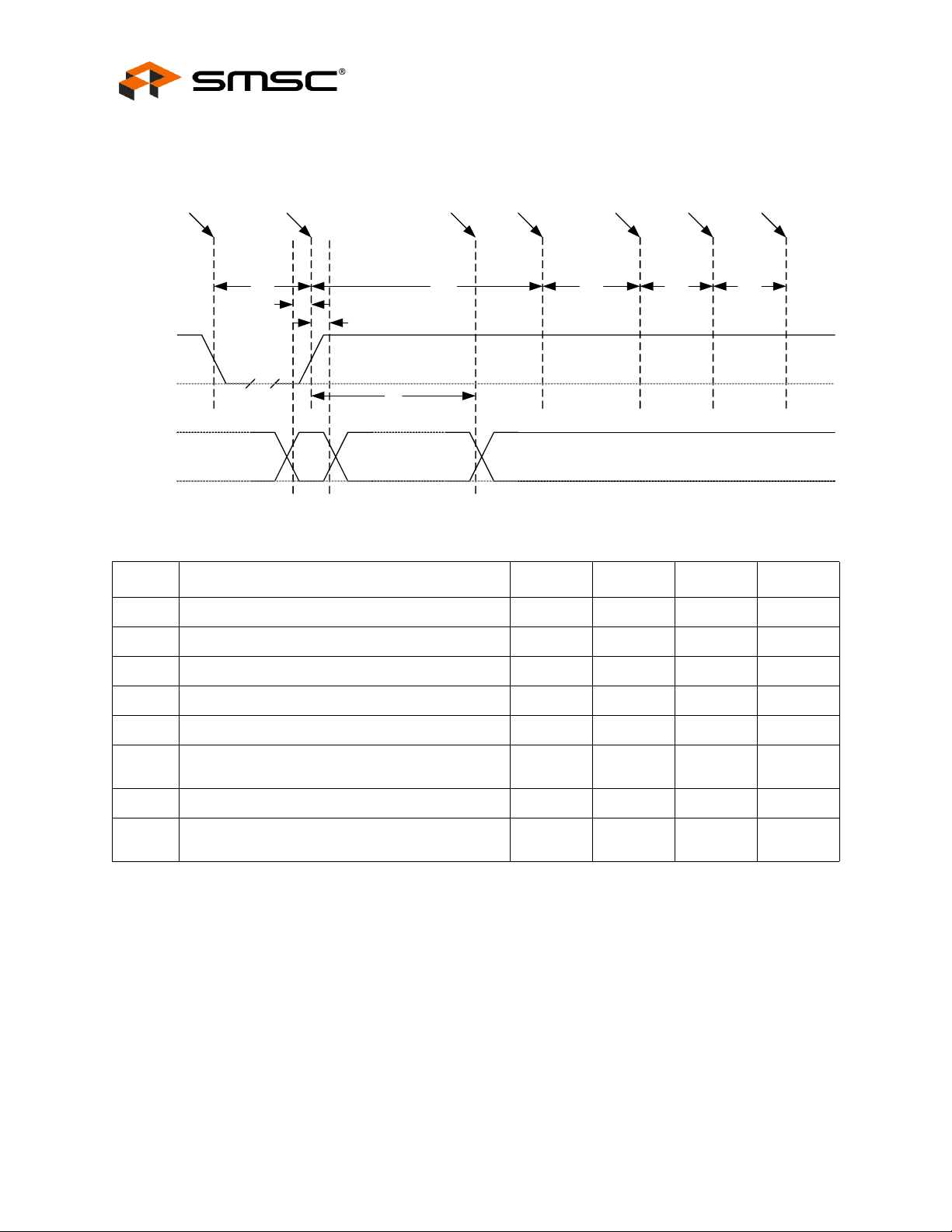
8.6.1.1 RESET_N for Strapping Option Configuration
USB 2.0 Hi-Speed Hub Controller
Datasheet
Hardware
reset
asserted
Read Strap
Options
t1
Drive Strap
Outputs to
inactive
levels
t5
Attach
USB
Upstream
USB Reset
recovery
t6
Idle
t7 t8
Start
completion
request
response
t2
RESET_N
VSS
t3
t4
Strap Pins
Don’t Care
VSS
NAME DESCRIPTION MIN TYP MAX UNITS
t1 RESET_N Asserted. 1 μsec
Valid Driven by Hub if strap is an output.
Don’t Care
Figure 8.3 Reset_N Timing for Default/Strap Option Mode
Table 8.7 Reset_N Timing for Default/Strap Option Mode
t2 Strap Setup Time 16.7 nsec
t3 Strap Hold Time. 16.7 1400 nsec
t4 hub outputs driven to inactive logic states 1.5 2 μsec
t5 USB Attach (See Note). 100 msec
t6 Host acknowledges attach and signals USB
100 msec
Reset.
t7 USB Idle. undefined msec
t8 Completion time for requests (with or without data
5 msec
stage).
Notes:
When in bus-powered mode, the hub and its associated circuitry must not consume more than 100
mA from the upstream USB power source during t1+t5.
All power supplies must have reached the operating levels mandated in Chapter 9, DC Parameters,
prior to (or coincident with) the assertion of RESET_N.
Revision 1.0 (3-11-09) 56 SMSC USB251x
DATASHEET
Page 57
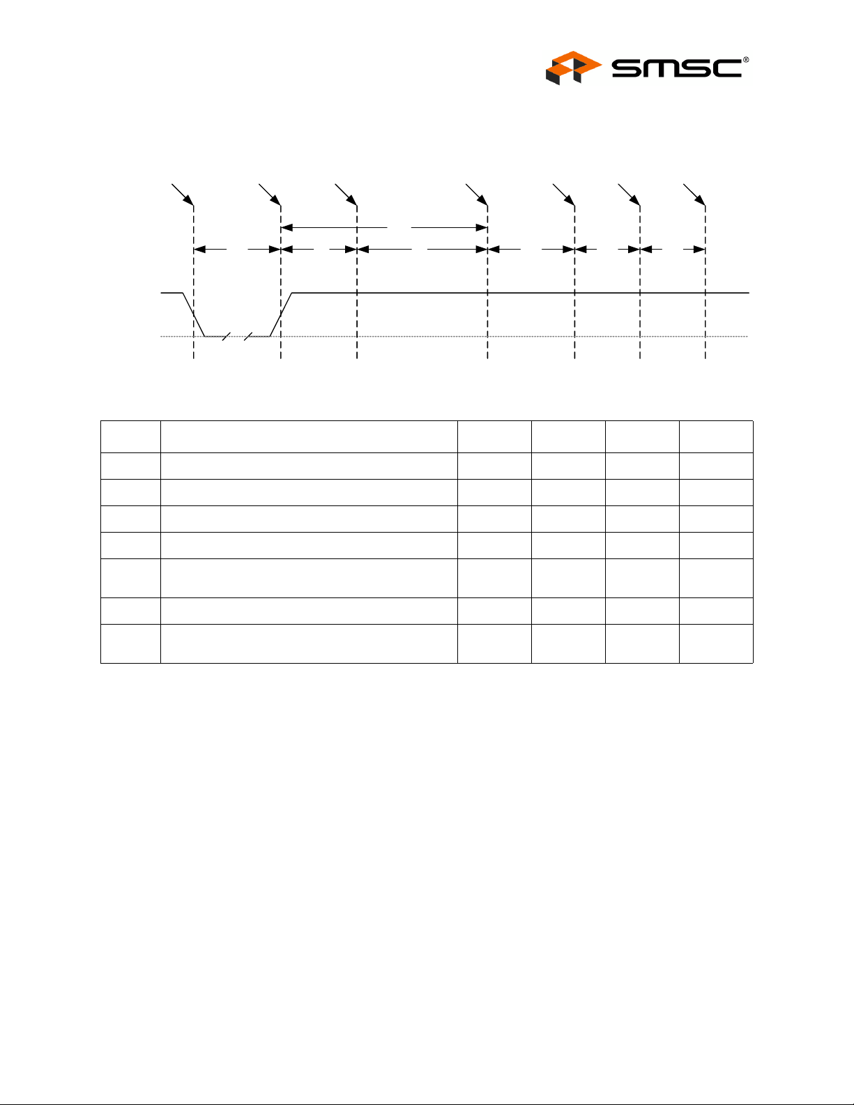
USB 2.0 Hi-Speed Hub Controller
Datasheet
8.6.1.2 RESET_N for EEPROM Configuration
Hardware
reset
asserted
Read Strap
Options
Read EEPROM
+
Set Options
Attach
USB
Upstream
USB Reset
recovery
Idle
Start
completion
request
response
t4
t6 t7
RESET_N
VSS
t1
t2
t3
t5
Figure 8.4 Reset_N Timing for EEPROM Mode
Table 8.8 Reset_N Timing for EEPROM Mode
NAME DESCRIPTION MIN TYP MAX UNITS
t1 RESET_N Asserted. 1 μsec
t2 Hub Recovery/Stabilization. 500 μsec
t3 EEPROM Read / Hub Config. 2.0 99.5 msec
t4 USB Attach (See Note). 100 msec
t5 Host acknowledges attach and signals USB
100 msec
Reset.
t6 USB Idle. undefined msec
t7 Completion time for requests (with or without data
5 msec
stage).
Notes:
When in bus-powered mode, the hub and its associated circuitry must not consume more than 100
mA from the upstream USB power source during t4+t5+t6+t7.
All power supplies must have reached the operating levels mandated in Chapter 9, DC Parameters,
prior to (or coincident with) the assertion of RESET_N.
SMSC USB251x 57 Revision 1.0 (3-11-09)
DATASHEET
Page 58

8.6.1.3 RESET_N for SMBus Slave Configuration
USB 2.0 Hi-Speed Hub Controller
Datasheet
Start
completion
request
response
RESET_N
VSS
Hardware
reset
asserted
Reset
Negation
t1
SMBus Code
Load
t2 t4
Hub PHY
Stabilization
t3
Attach
USB
Upstream
USB Reset
recovery
t5
Idle
t6 t7
Figure 8.5 Reset_N Timing for SMBus Mode
Table 8.9 Reset_N Timing for SMBus Mode
NAME DESCRIPTION MIN TYP MAX UNITS
t1 RESET_N Asserted. 1 μsec
t2 Hub Recovery/Stabilization. 500 μsec
t3 SMBus Code Load (See Note). 250 300 msec
t4 Hub Configuration and USB Attach. 100 msec
t5 Host acknowledges attach and signals USB
100 msec
Reset.
t6 USB Idle. Undefined msec
t7 Completion time for requests (with or without data
5 msec
stage).
Notes:
For bus-powered configurations, the 99.5 ms (MAX) is required, and the hub and its associated
circuitry must not consume more than 100 mA from the upstream USB power source during
t2+t3+t4+t5+t6+t7. For Self-Powered configurations, t3 MAX is not applicable and the time to load
the configuration is determined by the external SMBus host.
All power supplies must have reached the operating levels mandated in Chapter 9, DC Parameters,
prior to (or coincident with) the assertion of RESET_N.
8.6.2 USB Bus Reset
In response to the upstream port signaling a reset to the hub, the hub does the following:
Note: The hub does not propagate the upstream USB reset to downstream devices.
1. Sets default address to 0.
2. Sets configuration to: Unconfigured.
3. Negates PRTPWR[x:1] to all downstream ports unless battery charging (BC_EN) is enabled.
4. Clears all TT buffers.
5. Moves device from suspended to active (if suspended).
Revision 1.0 (3-11-09) 58 SMSC USB251x
DATASHEET
Page 59

USB 2.0 Hi-Speed Hub Controller
Datasheet
6. Complies with Section 11.10 of the USB 2.0 specification for behavior after completion of the reset
sequence. The host then configures the hub and the hub’s downstream port devices in accordance
with the USB specification.
Note: The hub does not propagate the upstream USB reset to downstream devices.
SMSC USB251x 59 Revision 1.0 (3-11-09)
DATASHEET
Page 60

USB 2.0 Hi-Speed Hub Controller
Chapter 9 DC Parameters
9.1 Maximum Guaranteed Ratings
PARAMETER SYMBOL MIN MAX UNITS COMMENTS
Datasheet
Storage
Temperature
Lead
Temperature
3.3 V supply
voltage
Voltage on any
I/O pin
Voltage on
XTALIN
Voltage on
XTALOUT
Note 9.1 Stresses above the specified parameters could cause permanent damage to the device.
Note 9.2 When powering this device from laboratory or system power supplies, it is important that
T
STOR
VDD33
PLLFILT
CRFILT
This is a stress rating only and functional operation of the device at any condition above
those indicated in the operation sections of this specification is not implied.
the absolute maximum ratings not be exceeded or device failure can result. Some power
supplies exhibit voltage spikes on their outputs when the AC power is switched on or off.
In addition, voltage transients on the AC power line may appear on the DC output. When
this possibility exists, it is suggested that a clamp circuit be used.
-55 150 °C
Refer to JEDEC Specification J-STD020D.
4.6 V Applies to all parts.
-0.5 5.5 V
-0.5 4.0 V
-0.5 2.5 V
9.2 Operating Conditions
PARAMETER SYMBOL MIN MAX UNITS COMMENTS
Commercial
Operating
Temperature
Industrial
Operating
Temperature
3.3 V supply voltage
3.3 V supply rise
time
Voltage on any I/O
pin
Voltage on XTALIN -0.3
Revision 1.0 (3-11-09) 60 SMSC USB251x
T
A
T
AI
VDD33 3.0 3.6 V Applies to all parts.
t
RT
0 70 °C Ambient temperature in still air.
Only applies to USB251x, USB251xA,
and USB251xB products.
-40 85 °C Ambient temperature in still air.
Only applies to USB251xi,
USB251xAi, and USB251xBi
products.
0 400 μs See Figure 9.1
-0.3 5.5 V If any 3.3 V supply voltage drops
below 3.0 V, then the MAX becomes:
(3.3 V supply voltage) + 0.5
VDD33 V
DATASHEET
Page 61

USB 2.0 Hi-Speed Hub Controller
Datasheet
Voltage
VDD33
PARAMETER SYMBOL MIN TYP MAX UNITS COMMENTS
I, IS Type Input Buffer
Low Input Level
High Input Level
Input Leakage
Hysteresis (‘IS’ Only)
Input Buffer with Pull-Up (IPU)
t
RT
10%
VSS
t
10%
t
90%
Figure 9.1 Supply Rise Time Model
Table 9.1 DC Electrical Characteristics
V
ILI
V
V
IHI
I
IL
HYSI
2.0
-10
250
90%
3.3 V
Time
0.8
+10
350
100%
V
V
μA
mV
TTL Levels
VIN = 0 to VDD33
Low Input Level
High Input Level
Low Input Leakage
High Input Leakage
Input Buffer with Pull-Down (IPD)
Low Input Level
High Input Level
Low Input Leakage
High Input Leakage
ICLK Input Buffer
Low Input Level
High Input Level
Input Leakage
V
V
V
ILI
V
IHI
I
ILL
I
IHL
V
ILI
V
IHI
I
ILL
I
IHL
ILCK
IHCK
I
IL
2.0
+35
-10
2.0
+10
-35
1.4
-10
0.8
+90
+10
0.8
-10
-90
0.5
+10
μA
μA
μA
μA
μA
V
TTL Levels
V
VIN = 0
VIN = VDD33
V
TTL Levels
V
VIN = 0
V
V
V
VIN = 0 to VDD33
= VDD33
IN
SMSC USB251x 61 Revision 1.0 (3-11-09)
DATASHEET
Page 62

Table 9.1 DC Electrical Characteristics (continued)
PARAMETER SYMBOL MIN TYP MAX UNITS COMMENTS
O12, I/O12 &I/OSD12 Type Buffer
USB 2.0 Hi-Speed Hub Controller
Datasheet
Low Output Level
High Output Level
Output Leakage
Hysteresis (‘SD’ pad only)
IO-U
(Note 2)
Supply Current Unconfigured
Hi-Speed Host
USB2512/12A/12B
USB2512i/12Ai/12Bi
USB2513/13B
USB2513i/13Bi
USB2514/14B
USB2514i/14Bi
USB2517
USB2517i
V
V
OH
I
OL
V
HYSC
I
CCINTHS
I
CCINTHS
I
CCINTHS
I
CCINTHS
I
CCINTHS
I
CCINTHS
I
CCINTHS
I
CCINTHS
OL
2.4
-10
250
90
90
95
95
95
95
120
120
0.4
+10
350
95
95
105
105
105
105
130
130
mA
mA
mA
mA
mA
mA
mA
mA
V
V
μA
mV
IOL = 12 mA @
VDD33 = 3.3 V
IOH = -12 mA @
VDD33 = 3.3 V
VIN = 0 to VDD33
(Note 9.1)
Supply Current Unconfigured
Full-Speed Host
USB2512/12A/12B
USB2512i/12Ai/12Bi
USB2513/13B
USB2513i/13Bi
USB2514/14B
USB2514i/14Bi
USB2517
USB2517i
I
CCINITFS
I
CCINITFS
I
CCINITFS
I
CCINITFS
I
CCINITFS
I
CCINITFS
I
CCINITFS
I
CCINITFS
80
80
80
80
80
80
105
105
85
85
90
90
90
90
115
115
mA
mA
mA
mA
mA
mA
mA
mA
Revision 1.0 (3-11-09) 62 SMSC USB251x
DATASHEET
Page 63

USB 2.0 Hi-Speed Hub Controller
Datasheet
PARAMETER SYMBOL MIN TYP MAX UNITS COMMENTS
Supply Current Configured
Hi-Speed Host, 1 downstream port
Table 9.1 DC Electrical Characteristics (continued)
USB2512/12A/12B
USB2512i/12Ai/12Bi
USB2513/13B
USB2513i/13Bi
USB2514/14B
USB2514i/14Bi
USB2517
USB2517i
Supply Current Configured
Hi-Speed Host, each additional
downstream port
Supply Current Configured
Full-Speed Host, 1 downstream port
USB2512/12A/12B
USB2512i/12Ai/12Bi
USB2513/13B
USB2513i/13Bi
USB2514/14B
USB2514i/14Bi
USB2517
USB2517i
I
HCH1
I
HCH1
I
HCH1
I
HCH1
I
HCH1
I
HCH1
I
HCH1
I
HCH1
I
FCC1
I
FCC1
I
FCC1
I
FCC1
I
FCC1
I
FCC1
I
FCC1
I
FCC1
130
130
150
150
155
155
240
240
1 port
base
+
15 mA
105
105
125
125
140
140
215
215
155
160
180
185
200
205
275
280
1 port
base
+
40 mA
125
135
135
140
150
155
220
225
mA
mA
mA
mA
mA
mA
mA
mA
mA
mA
mA
mA
mA
mA
mA
mA
mA
Supply Current Configured
Full-Speed Host, each additional
downstream port
SMSC USB251x 63 Revision 1.0 (3-11-09)
1 port
base
0 mA
1 port
base
+
+
0 mA
mA
There is no
additional current for
additional ports.
DATASHEET
Page 64
USB 2.0 Hi-Speed Hub Controller
Datasheet
Table 9.1 DC Electrical Characteristics (continued)
PARAMETER SYMBOL MIN TYP MAX UNITS COMMENTS
Supply Current Suspend
USB2512/12A/12B
USB2512i/12Ai/12Bi
USB2513/13B
USB2513i/13Bi
USB2514/14B
USB2514i/14Bi
USB2517
USB2517i
Supply Current Reset
USB2512/12A/12B
USB2512i/12Ai/12Bi
USB2513/13B
USB2513i/13Bi
USB2514/14B
USB2514i/14Bi
USB2517
USB2517i
I
CSBY
I
CSBY
I
CSBY
I
CSBY
I
CSBY
I
CSBY
I
CSBY
I
CSBY
I
CRST
I
CRST
I
CRST
I
CRST
I
CRST
I
CRST
I
CRST
I
CRST
310
310
310
310
310
310
310
310
105
105
100
100
100
100
115
115
420
600
420
550
420
600
610
800
275
400
230
350
275
400
320
600
μA
μA
μA
μA
μA
μA
μA
μA
μA
μA
μA
μA
μA
μA
μA
μA
All supplies
combined
All supplies
combined
Note 9.3 Output leakage is measured with the current pins in high impedance.
Note 9.4 See USB 2.0 specification for USB DC electrical characteristics.
Revision 1.0 (3-11-09) 64 SMSC USB251x
DATASHEET
Page 65
USB 2.0 Hi-Speed Hub Controller
Datasheet
Table 9.2 Pin Capacitance
LIMITS
PARAMETER SYMBOL MIN TYP MAX UNIT TEST CONDITION
Clock Input
C
Capacitance
Input Capacitance C
Output Capacitance C
Note 9.5 Capacitance TA = 25°C; fc = 1 MHz; VDD33 = 3.3 V
XTAL
IN
OUT
2 pF All pins except USB pins and the pins
under the test tied to AC ground.
10 pF (See Note 9.5)
20 pF
SMSC USB251x 65 Revision 1.0 (3-11-09)
DATASHEET
Page 66
Chapter 10 AC Specifications
10.1 Oscillator/Clock
Crystal: Parallel Resonant, Fundamental Mode, 24/481 MHz ±350 ppm.
External Clock: 50% Duty cycle ± 10%, 24/48 MHz ± 350 ppm, Jitter < 100 ps rms.
C
1
USB 2.0 Hi-Speed Hub Controller
XTAL1
(C
S1 = CB
+ C
XTAL
Datasheet
)
Crystal
C
2
Note: CB equals total board/trace capacitance.
C
L
Figure 10.1 Typical Crystal Circuit
(C1 + CS1) x (C2 + CS2)
=
C
L
+ C
(C
1
Figure 10.2 Formula to Find the Value of C
C = (2 x CL) - C
Figure 10.3 Simplified Form of the Capacitance Formula
S1 + C2
1 Meg
+ CS2)
and C
1
s
XTAL2
(C
S2 = CB
2
+ C
XTAL
)
10.1.1 SMBus Interface:
The SMSC Hub conforms to all voltage, power, and timing characteristics and specifications as set
forth in the SMBus 1.0 specification for Slave-Only devices (except as noted in Section 8.3).
10.1.2 I2C EEPROM:
Clock frequency is fixed at 60 KHz ± 20%.
10.1.3 USB 2.0
The SMSC Hub conforms to all voltage, power, and timing characteristics and specifications as set
forth in the USB 2.0 specification. Please refer to the USB 2.0 specification for more information.
1.Only when SEL48 is available and supported.
Revision 1.0 (3-11-09) 66 SMSC USB251x
DATASHEET
Page 67
Revision 1.0 (3-11-09) 67 SMSC USB251x
Chapter 11 Package Outlines
DATASHEET
USB 2.0 High-Speed 2-Port Hub Controller
Datasheet
Figure 11.1 36-Pin QFN, 6x6 mm Body, 0.5 mm Pitch
Page 68
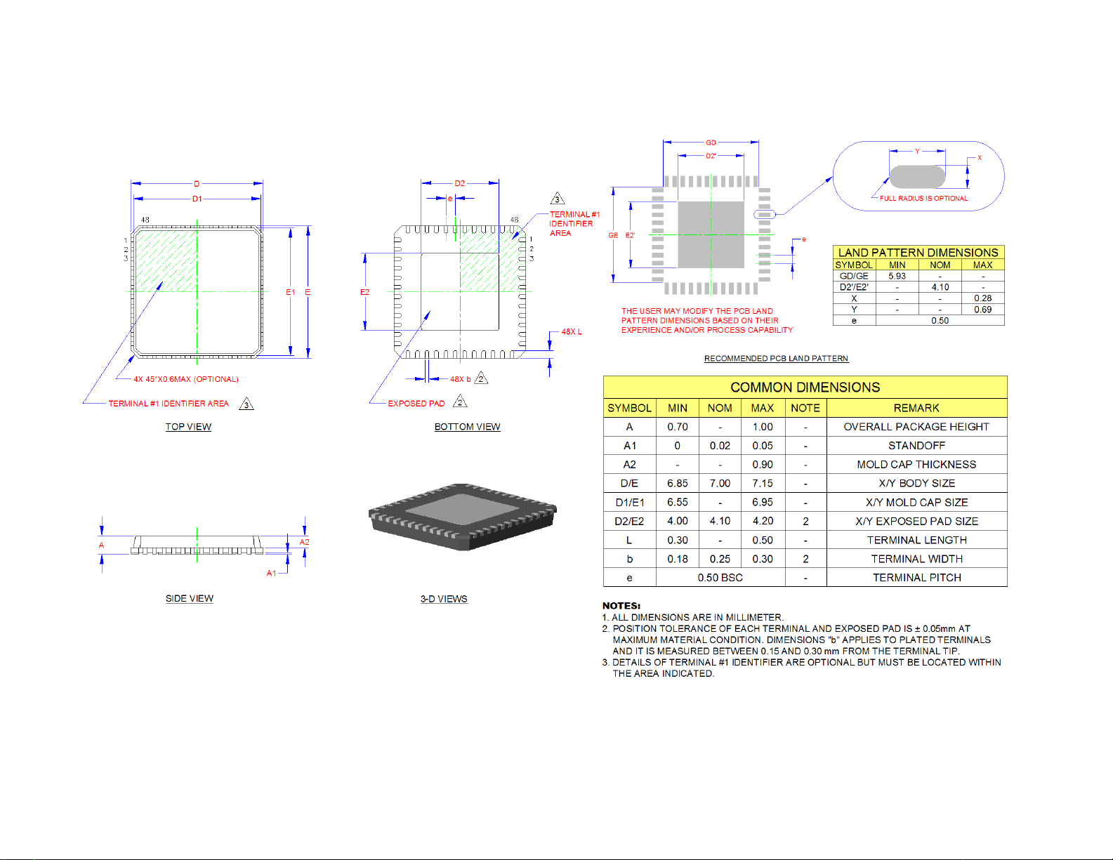
Revision 1.0 (3-11-09) 68 SMSC USB251x
DATASHEET
USB 2.0 High-Speed 2-Port Hub Controller
Datasheet
Figure 11.2 48-Pin QFN, 7x7 mm Body, 0.5 mm Pitch
Page 69
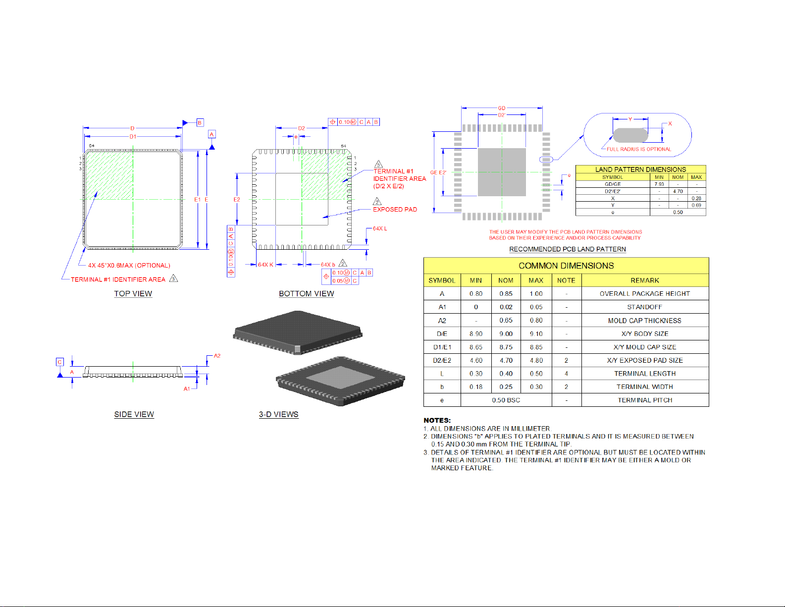
Revision 1.0 (3-11-09) 69 SMSC USB251x
DATASHEET
USB 2.0 High-Speed 2-Port Hub Controller
Datasheet
Figure 11.3 64-Pin QFN, 9x9 mm Body, 0.5 mm Pitch
Page 70
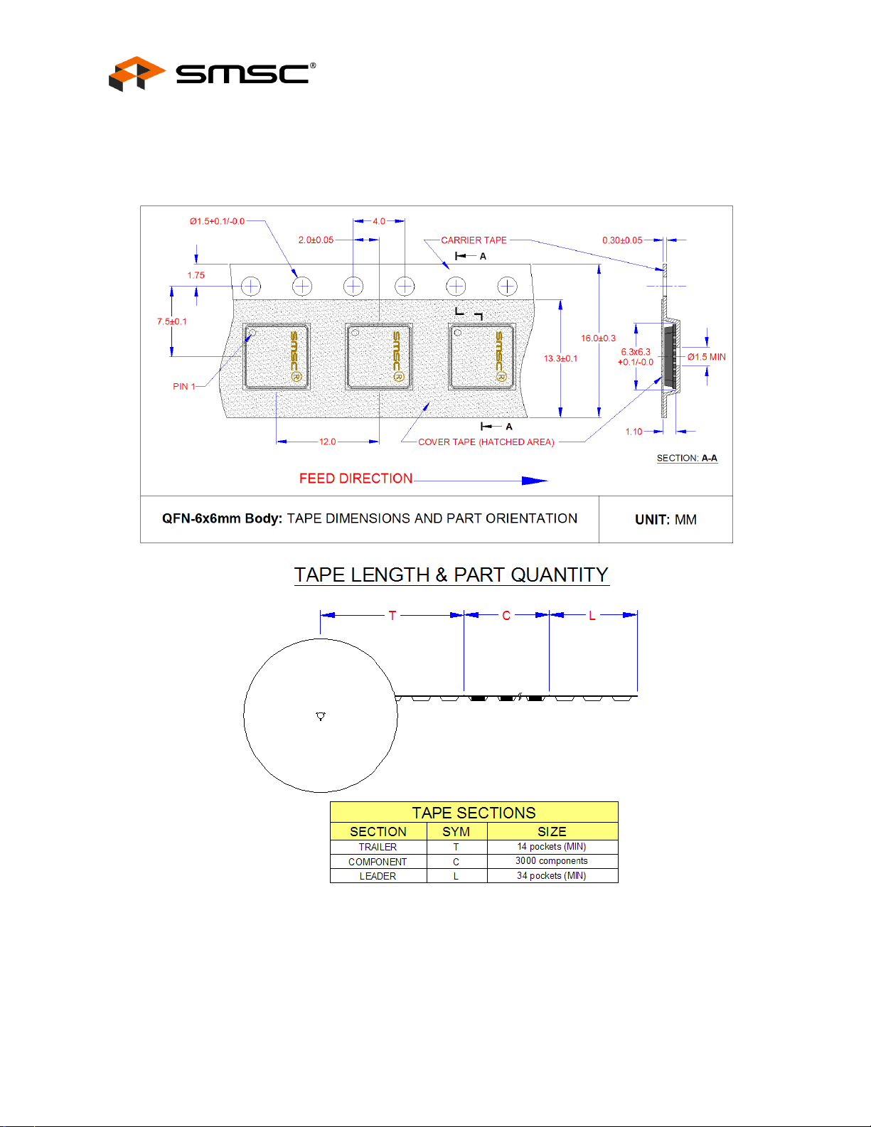
11.1 Tape and Reel Specifications
USB 2.0 Hi-Speed Hub Controller
Datasheet
Figure 11.4 36-Pin Package Tape Specifications
Revision 1.0 (3-11-09) 70 SMSC USB251x
DATASHEET
Page 71
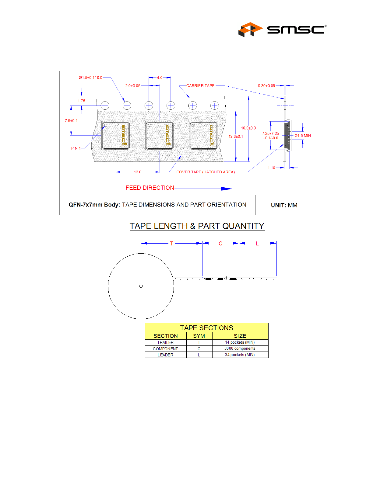
USB 2.0 Hi-Speed Hub Controller
Datasheet
Figure 11.5 48-Pin Package Tape Specifications
SMSC USB251x 71 Revision 1.0 (3-11-09)
DATASHEET
Page 72
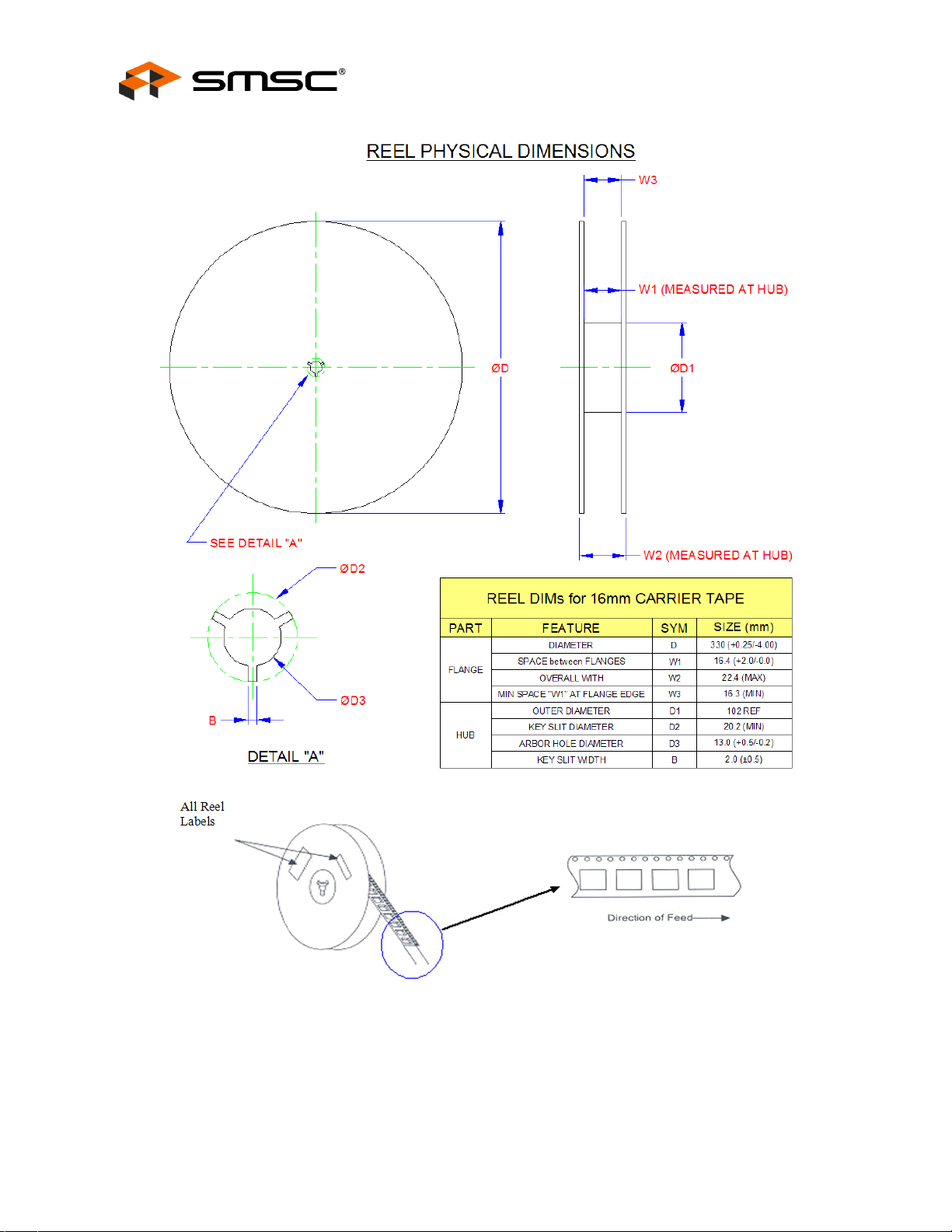
USB 2.0 Hi-Speed Hub Controller
Datasheet
Figure 11.6 36-Pin and 48-Pin Package Reel Specifications
Revision 1.0 (3-11-09) 72 SMSC USB251x
DATASHEET
 Loading...