

Page 1

USB2504/
USB2504A
Integrated USB 2.0
Compatible 4-Port Hub
PRODUCT FEATURES
Integra ted USB 2.0 Compatible 4-Port Hub
— 4 Transaction Translators for highest performance
— High-Speed (480Mbits/s), Full-Speed (12Mbits/s) and
Low-Speed (1.5Mbits/s) compatible
— Full power management with per port or ganged
selectable power control
— Detects Bus-Power/Self-Power source and changes
mode automatically
Co mplete USB Specification 2.0 Compatibility
— Includes USB 2.0 Transceivers
VID/PID/DID, and Port Configuration for Hub via:
— Single Serial I2C EEPROM
— SMBus Slave Port
De fault VID/PID/DID, allows functionality when
configuration EEPROM is absent
Ha rdware Strapping options allow for configuration
without an external EEPROM or SMBus Host
,
Datasheet
On-Boa rd 24MHz Crystal Driver Circuit or 24 MHz
external clock driver
Interna l PLL for 480MHz USB 2.0 Sampling
Interna l 1.8V Linear Voltage Regulator
Integ rated USB termination and Pull-up/Pull-down
resistors
Interna l Short Circuit protection of USB differential
signal pins
1 .8 Volt Low Power Core Operation
3 .3 Volt I/O with 5V Input Tolerance
6 4-Pin TQFP lead-free RoHS compliant package
SMSC USB2504/USB2504A DATASHEET Revision 2.3 (08-27-07)
Page 2

Integrated USB 2.0 Compatible 4-Port Hub
ORDER NUMBERS:
USB2504/USB2504A-JT FOR 64 PIN TQFP LEAD-FREE ROHS COMPLIANT PACKAGE
Datasheet
80 ARKAY DRIVE, HAUPPAUGE, NY 11788 (631) 435-6000, FAX (631) 273-3123
Copyright © 2007 SMSC or its subsidiaries. All rights reserved.
Circuit diagrams and other information relating to SMSC products are included as a mean s of illustrating typical applications. Conse quently, complete information sufficient for
construction purposes is not necessarily given. Although the information has been checked and is believed to be accurate, no responsibility is assumed for inaccuracies. SMSC
reserves the right to make changes to specifications and product descriptions at any time without notice. Contact your local SMSC sales office to obtain the latest specifications
before placing your product order. The provision of this information does not convey to the purchaser of the described semiconductor devices any licenses under any patent
rights or other intellectual property rights of SMSC or others. All sales are expressly conditional on your agreement to the terms and conditions of the most recently da ted
version of SMSC's standard Terms of Sale Agreement dated before the date of your order (the "Terms of Sale Agreement"). The product may contain design defects or errors
known as anomalies which may cause the product's functions to deviate from published specifications. Anomaly sheets are available upon request. SMSC products are not
designed, intended, authorized or warranted for use in any life support or other application where product failure could cause or contribute to personal injury or severe property
damage. Any and all such uses without prior written approval of an Officer of SMSC and further testing and/or modification will be fully at the risk of the customer. Copies of
this document or other SMSC literature, as well as the Terms of Sale Agreement, may be obtained by visiting SMSC’s website at http://www.smsc.com. SMSC is a registered
trademark of Standard Microsystems Corporation (“SMSC”). Product names and company names are the trademarks of their respective holders.
SMSC DISCLAIMS AND EXCLUDES ANY AND ALL WARRANTIES, INCLUDING WITHOUT LIMITATION ANY AND ALL IMPLIED WARRANTIES OF MERCHANTABILITY,
FITNESS FOR A PARTICULAR PURPOSE, TITLE, AND AGAINST INFRINGEMENT AND THE LIKE, AND ANY AND ALL WARRANTIES ARISING FROM ANY COURSE
OF DEALING OR USAGE OF TRADE. IN NO EVENT SHALL SMSC BE LIABLE FOR ANY DIRECT, INCIDENTAL, INDIRECT, SPECIAL, PUNITIVE, OR CONSEQUENTIAL
DAMAGES; OR FOR LOST DATA, PROFITS, SAVINGS OR REVENUES OF ANY KIND; REGARDLESS OF THE FORM OF ACTION, WHETHER BASED ON CONTRACT;
TORT; NEGLIGENCE OF SMSC OR OTHERS; STRICT LIABILITY; BREACH OF WARRANTY; OR OTHERWISE; WHETHER OR NOT ANY REMEDY OF BUYER IS HELD
TO HAVE FAILED OF ITS ESSENTIAL PURPOSE, AND WHETHER OR NOT SMSC HAS BEEN ADVISED OF THE POSSIBILITY OF SUCH DAMAGES.
Revision 2.3 (08-27-07) 2 SMSC USB2504/USB2504A
DATASHEET
Page 3

Integrated USB 2.0 Compatible 4-Port Hub
Datasheet
Table of Contents
Chapter 1 General Description. . . . . . . . . . . . . . . . . . . . . . . . . . . . . . . . . . . . . . . . . . . . . . . . . 7
1.1 OEM Selectable Features. . . . . . . . . . . . . . . . . . . . . . . . . . . . . . . . . . . . . . . . . . . . . . . . . . . . . . . . . 7
Chapter 2 Pin Table 4-Port. . . . . . . . . . . . . . . . . . . . . . . . . . . . . . . . . . . . . . . . . . . . . . . . . . . . 8
Chapter 3 Pin Configuration 4-Port Hub . . . . . . . . . . . . . . . . . . . . . . . . . . . . . . . . . . . . . . . . 9
Chapter 4 4-Port Hub Block Diagram. . . . . . . . . . . . . . . . . . . . . . . . . . . . . . . . . . . . . . . . . . 10
Chapter 5 Functional Block Description . . . . . . . . . . . . . . . . . . . . . . . . . . . . . . . . . . . . . . . . 16
5.1 4-Port Hub . . . . . . . . . . . . . . . . . . . . . . . . . . . . . . . . . . . . . . . . . . . . . . . . . . . . . . . . . . . . . . . . . . . 16
5.1.1 Hub Configuration Options . . . . . . . . . . . . . . . . . . . . . . . . . . . . . . . . . . . . . . . . . . . . . . . 16
5.1.2 VBus Detect. . . . . . . . . . . . . . . . . . . . . . . . . . . . . . . . . . . . . . . . . . . . . . . . . . . . . . . . . . . 19
5.2 EEPROM Interface. . . . . . . . . . . . . . . . . . . . . . . . . . . . . . . . . . . . . . . . . . . . . . . . . . . . . . . . . . . . . 19
5.2.1 I2C EEPROM . . . . . . . . . . . . . . . . . . . . . . . . . . . . . . . . . . . . . . . . . . . . . . . . . . . . . . . . . 19
5.2.2 In-Circuit EEPROM Programming. . . . . . . . . . . . . . . . . . . . . . . . . . . . . . . . . . . . . . . . . . 20
5.2.3 EEPROM DATA . . . . . . . . . . . . . . . . . . . . . . . . . . . . . . . . . . . . . . . . . . . . . . . . . . . . . . . 20
5.3 SMBus Slave Interface . . . . . . . . . . . . . . . . . . . . . . . . . . . . . . . . . . . . . . . . . . . . . . . . . . . . . . . . . . 25
5.3.1 Bus Protocols . . . . . . . . . . . . . . . . . . . . . . . . . . . . . . . . . . . . . . . . . . . . . . . . . . . . . . . . . 25
5.3.2 Invalid Protocol Response Behavior . . . . . . . . . . . . . . . . . . . . . . . . . . . . . . . . . . . . . . . . 26
5.3.3 General Call Address Response . . . . . . . . . . . . . . . . . . . . . . . . . . . . . . . . . . . . . . . . . . . 26
5.3.4 Slave Device Time-Out . . . . . . . . . . . . . . . . . . . . . . . . . . . . . . . . . . . . . . . . . . . . . . . . . . 27
5.3.5 Stretching the SCLK Signal. . . . . . . . . . . . . . . . . . . . . . . . . . . . . . . . . . . . . . . . . . . . . . . 27
5.3.6 SMBus Timing . . . . . . . . . . . . . . . . . . . . . . . . . . . . . . . . . . . . . . . . . . . . . . . . . . . . . . . . . 27
5.3.7 Bus Reset Sequence. . . . . . . . . . . . . . . . . . . . . . . . . . . . . . . . . . . . . . . . . . . . . . . . . . . . 27
5.3.8 SMBus Alert Response Address. . . . . . . . . . . . . . . . . . . . . . . . . . . . . . . . . . . . . . . . . . . 27
5.3.9 Internal SMBus Memory Register Set . . . . . . . . . . . . . . . . . . . . . . . . . . . . . . . . . . . . . . . 27
5.4 Default Configuration Option: . . . . . . . . . . . . . . . . . . . . . . . . . . . . . . . . . . . . . . . . . . . . . . . . . . . . . 33
5.5 Default Strapping Options: . . . . . . . . . . . . . . . . . . . . . . . . . . . . . . . . . . . . . . . . . . . . . . . . . . . . . . . 33
5.6 Reset . . . . . . . . . . . . . . . . . . . . . . . . . . . . . . . . . . . . . . . . . . . . . . . . . . . . . . . . . . . . . . . . . . . . . . . 34
5.6.1 External Hardware RESET_N . . . . . . . . . . . . . . . . . . . . . . . . . . . . . . . . . . . . . . . . . . . . . 34
5.6.2 USB Bus Reset . . . . . . . . . . . . . . . . . . . . . . . . . . . . . . . . . . . . . . . . . . . . . . . . . . . . . . . . 37
Chapter 6 Backward Compatibility to the USB20H04. . . . . . . . . . . . . . . . . . . . . . . . . . . . . 39
6.1 Internal 1.8V regulator . . . . . . . . . . . . . . . . . . . . . . . . . . . . . . . . . . . . . . . . . . . . . . . . . . . . . . . . . . 39
6.2 Configuration by Internal Defaults . . . . . . . . . . . . . . . . . . . . . . . . . . . . . . . . . . . . . . . . . . . . . . . . . 39
6.3 Configuration by SMBus. . . . . . . . . . . . . . . . . . . . . . . . . . . . . . . . . . . . . . . . . . . . . . . . . . . . . . . . . 39
6.4 PRTPWR_POL. . . . . . . . . . . . . . . . . . . . . . . . . . . . . . . . . . . . . . . . . . . . . . . . . . . . . . . . . . . . . . . . 39
Chapter 7 XNOR Test . . . . . . . . . . . . . . . . . . . . . . . . . . . . . . . . . . . . . . . . . . . . . . . . . . . . . . . 40
Chapter 8 DC Parameters. . . . . . . . . . . . . . . . . . . . . . . . . . . . . . . . . . . . . . . . . . . . . . . . . . . . 41
8.1 Maximum Guaranteed Ratings. . . . . . . . . . . . . . . . . . . . . . . . . . . . . . . . . . . . . . . . . . . . . . . . . . . . 41
8.2 Recommended Operating Conditions. . . . . . . . . . . . . . . . . . . . . . . . . . . . . . . . . . . . . . . . . . . . . . . 42
Chapter 9 AC Specifications. . . . . . . . . . . . . . . . . . . . . . . . . . . . . . . . . . . . . . . . . . . . . . . . . . 45
9.1 Oscillator/Clock. . . . . . . . . . . . . . . . . . . . . . . . . . . . . . . . . . . . . . . . . . . . . . . . . . . . . . . . . . . . . . . . 45
9.1.1 SMBus Interface:. . . . . . . . . . . . . . . . . . . . . . . . . . . . . . . . . . . . . . . . . . . . . . . . . . . . . . . 45
9.1.2 I2C EEPROM: . . . . . . . . . . . . . . . . . . . . . . . . . . . . . . . . . . . . . . . . . . . . . . . . . . . . . . . . . 45
9.1.3 USB 2.0 . . . . . . . . . . . . . . . . . . . . . . . . . . . . . . . . . . . . . . . . . . . . . . . . . . . . . . . . . . . . . . 45
SMSC USB2504/USB2504A 3 Revision 2.3 (08-27-07)
DATASHEET
Page 4

Integrated USB 2.0 Compatible 4-Port Hub
Datasheet
Chapter 10 Package Outline . . . . . . . . . . . . . . . . . . . . . . . . . . . . . . . . . . . . . . . . . . . . . . . . . . . 46
Revision 2.3 (08-27-07) 4 SMSC USB2504/USB2504A
DATASHEET
Page 5

Integrated USB 2.0 Compatible 4-Port Hub
Datasheet
List of Figures
Figure 3.1 4-Port 64 Pin TQFP . . . . . . . . . . . . . . . . . . . . . . . . . . . . . . . . . . . . . . . . . . . . . . . . . . . . . . . . . 9
Figure 4.1 4-Port Block Diagram. . . . . . . . . . . . . . . . . . . . . . . . . . . . . . . . . . . . . . . . . . . . . . . . . . . . . . . 10
Figure 5.1 LED Strapping Option . . . . . . . . . . . . . . . . . . . . . . . . . . . . . . . . . . . . . . . . . . . . . . . . . . . . . . 34
Figure 5.2 Reset_N Timing for Default/Strap Option Mode. . . . . . . . . . . . . . . . . . . . . . . . . . . . . . . . . . . 35
Figure 5.3 Reset_N Timing for EEPROM Mode . . . . . . . . . . . . . . . . . . . . . . . . . . . . . . . . . . . . . . . . . . . 36
Figure 5.4 Reset_N Timing for SMBus Mode . . . . . . . . . . . . . . . . . . . . . . . . . . . . . . . . . . . . . . . . . . . . . 37
Figure 10.1 64 Pin TQFP Package Outline (10x10x1.4 mm body - 2 mm footprint). . . . . . . . . . . . . . . . . 46
SMSC USB2504/USB2504A 5 Revision 2.3 (08-27-07)
DATASHEET
Page 6

Integrated USB 2.0 Compatible 4-Port Hub
Datasheet
List of Tables
Table 2.1 4-Port Pin Table for 64-TQFP . . . . . . . . . . . . . . . . . . . . . . . . . . . . . . . . . . . . . . . . . . . . . . . . . . 8
Table 4.1 4-Port Hub Pin Descriptions . . . . . . . . . . . . . . . . . . . . . . . . . . . . . . . . . . . . . . . . . . . . . . . . . . 10
Table 4.2 SMBus or EEPROM Interface Behavior . . . . . . . . . . . . . . . . . . . . . . . . . . . . . . . . . . . . . . . . . 13
Table 4.3 Miscellaneous Pins . . . . . . . . . . . . . . . . . . . . . . . . . . . . . . . . . . . . . . . . . . . . . . . . . . . . . . . . . 13
Table 4.4 Power, Ground, and No Connect. . . . . . . . . . . . . . . . . . . . . . . . . . . . . . . . . . . . . . . . . . . . . . . 14
Table 4.5 Buffer Type Descriptions . . . . . . . . . . . . . . . . . . . . . . . . . . . . . . . . . . . . . . . . . . . . . . . . . . . . . 15
Table 5.1 User-Defined Descriptor Data . . . . . . . . . . . . . . . . . . . . . . . . . . . . . . . . . . . . . . . . . . . . . . . . . 20
Table 5.2 SMBus Write Byte Protocol . . . . . . . . . . . . . . . . . . . . . . . . . . . . . . . . . . . . . . . . . . . . . . . . . . . 26
Table 5.3 SMBus Read Byte Protocol. . . . . . . . . . . . . . . . . . . . . . . . . . . . . . . . . . . . . . . . . . . . . . . . . . . 26
Table 5.4 SMBus Slave Interface Register Map . . . . . . . . . . . . . . . . . . . . . . . . . . . . . . . . . . . . . . . . . . . 27
Table 5.5 Reset_N Timing for Default/Strap Option Mode . . . . . . . . . . . . . . . . . . . . . . . . . . . . . . . . . . . 35
Table 5.6 Reset_N Timing for EEPROM Mode . . . . . . . . . . . . . . . . . . . . . . . . . . . . . . . . . . . . . . . . . . . . 36
Table 5.7 Reset_N Timing for SMBus Mode. . . . . . . . . . . . . . . . . . . . . . . . . . . . . . . . . . . . . . . . . . . . . . 37
Table 8.1 DC Electrical Characteristics . . . . . . . . . . . . . . . . . . . . . . . . . . . . . . . . . . . . . . . . . . . . . . . . . . 42
Table 10.1 64 Pin TQFP Package Parameters . . . . . . . . . . . . . . . . . . . . . . . . . . . . . . . . . . . . . . . . . . . . . 46
Revision 2.3 (08-27-07) 6 SMSC USB2504/USB2504A
DATASHEET
Page 7

Integrated USB 2.0 Compatible 4-Port Hub
Datasheet
Chapter 1 General Description
The SMSC 4-Port Hub is fully compliant with the USB 2.0 Specification and will attach to a USB host
as a Full-Speed Hub or as a Full-/High-Speed Hub. The 4-Port Hub supports Low-Speed, Full-Speed,
and High-Speed (if operating as a High-Speed Hub) downstream devices on all of the enabled
downstream ports.
A dedicated Transaction Translator (TT) is available for each downstream facing port. This architecture
ensures maximum USB throughput for each connected device when operating with mixed-speed
peripherals.
The Hub works with an external USB power distribution switch device to control V
downstream ports, and to limit current and sense over-current conditions.
All required resistors on the USB ports are integrated into the Hub. This includes all seri es termination
resistors on D+ and D– pins and all require d pull-down and pull-up resistors on D+ and D– pins. The
over-current sense inputs for the downstream facing ports have internal pull-up resistors.
Throughout this document the upstream facing port of the hub will be referred to as the upstream port,
and the downstream facing ports will be called the downstream ports.
1.1 OEM Selectable Features
A default configuration is available in the USB2504/USB2504A following a reset. This configuration
may be sufficient for some applications. Strapping option pins make it possible to modify a limited subset of the configuration options.
The USB2504/USB2504A may also be configured by an external EEPROM o r a microcontroller. When
using the microcontroller interface, the Hub appears as an SMBus slave device. If the Hub is pinstrapped for external EEPROM configuration but no external EEPROM is present, then a value of ‘0’
will be written to all configuration data bit fields (the hub will attach to the host with all ‘0’ values).
The 4-Port Hub supports several OEM selectable features:
Operation as a Self-Powered USB Hub or as a Bus-Powered USB Hub.
Operation as a Dynamic-Powered Hub (Hub operate s as a Bus-Powered device if a local power
source is not available and switches to Self-Powered opera tion when a local power source is
available).
Multiple Transaction Translator (Multi-TT) or Single-TT support.
Optional OEM configuration via I2C EEPROM or via the industry standard SMBus interface from
an external SMBus Host.
Port power switching on an individual or ganged basis.
Port over-current monitoring on an individual or ganged basis.
LED indicator support.
Compound device support (port is permanently hardwired to a down strea m USB perip heral device).
Hardware strapping options enable configuration of the following feature s.
Non-Removable Ports
Port Power Polarity (active high or active low logic)
Port Disable
LED support
MTT enable
Ganged Vs Port power switching and over-current sensing
switching to
BUS
SMSC USB2504/USB2504A 7 Revision 2.3 (08-27-07)
DATASHEET
Page 8
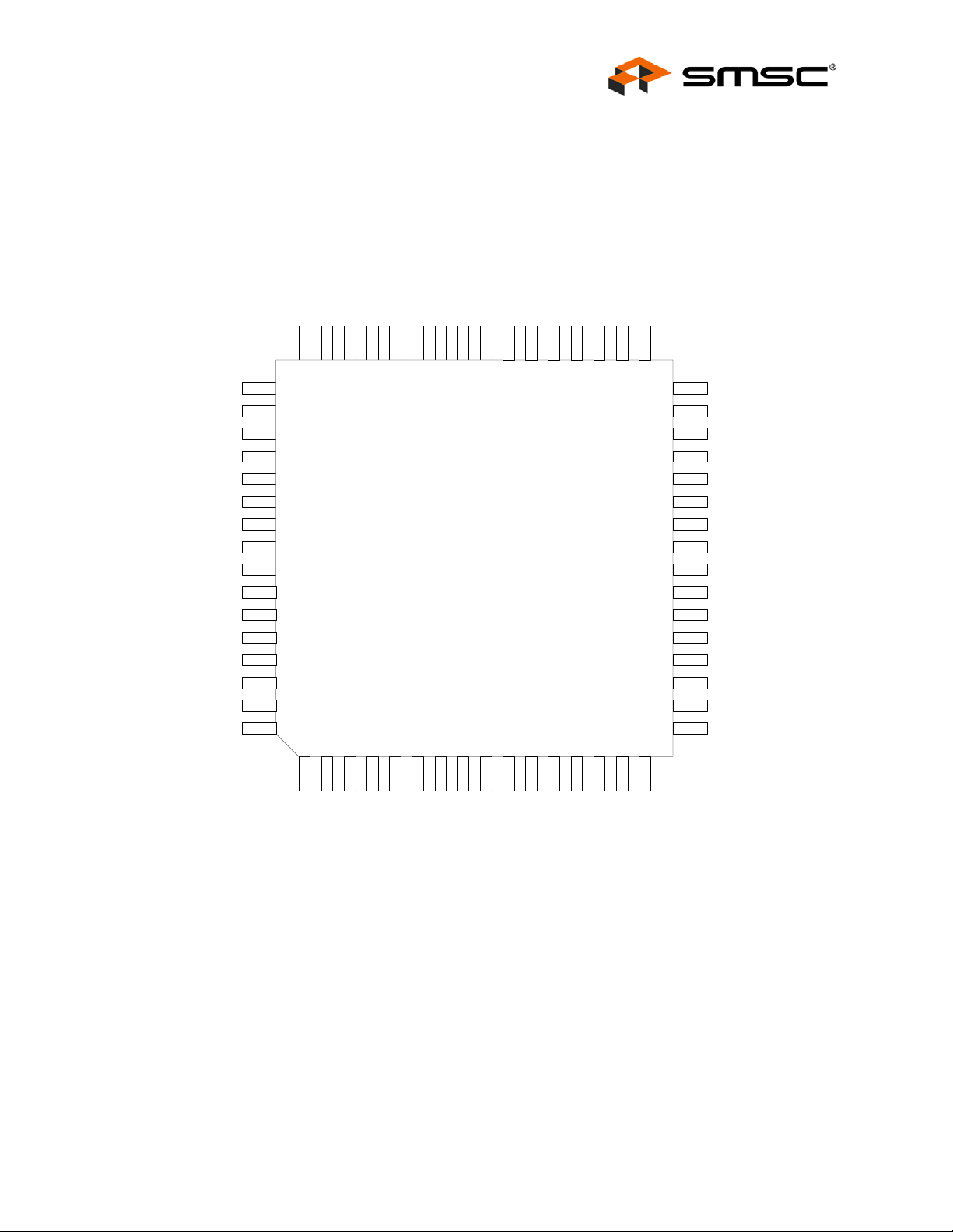
Chapter 2 Pin Table 4-Port
Table 2. 1 4-Port Pin Table for 64-TQF P
UPSTREAM USB 2.0 INTERFACE (3 PINS)
USBDP0 USBDN0 VBUS_DET
4-PORT USB 2.0 INTERFACE (26 PINS)
USBDP1 USBDN1 USBDP2 USBDN2
USBDP3 USBDN3 USBDP4 USBDN4
Integrated USB 2.0 Compatible 4-Port Hub
Datasheet
GR1/
NON_REM0
AM1/
GANG_EN
PRTPWR1 PRTPWR2 PRTPWR3 PRTPWR4
OCS1_N OCS2_N OCS3_N OCS4_N
PRTPWR_POL RBIAS
SDA/SMBDATA SCL/SMBCLK/ CFG_SEL2 CFG_SEL1
CFG_SEL0
XTAL1/CLKIN XTAL2 RESET_N SELF_PWR
ATEST/
REG_EN
POWER, GROUND (17 PINS) AND (5) NO CONNECT
GR2/
NON_REM1
AM2/
MTT_EN
SERIAL PORT INTERFACE (5 PINS)
MISC (8 PINS)
CLKIN_EN TEST1 TEST0
GR3/
PRT_DIS0
AM3 AM4/
GR4/
PRT_DIS1
LED_EN
Revision 2.3 (08-27-07) 8 SMSC USB2504/USB2504A
DATASHEET
Page 9
Integrated USB 2.0 Compatible 4-Port Hub
Datasheet
Chapter 3 Pin Configuration 4-Port Hub
RESET_N
CFG_SEL1
SELF_PWR
VBUS_DET
VSS
VDD18
VSS
NC
XTAL2
XTAL1/CLKIN
CFG_SEL2
VDDA18PLL
VDDA33PLL
ATEST/REG_EN
RBIAS
VSS
49
64
TEST1
48
1
CLKIN_EN
PRTPWR2
OCS2_N
OCS1_N
PRTPWR1
USB2504 &
USB2504A
OCS3_N
VDD18
VSS
PRTPWR4
PRTPWR3
CFG_SEL0
OCS4_N
SCL/SMBCLK
NC
SDA/SMBDATA
33
16
32
17
NC
TEST0
VDD18
VSS
VDD33
GR1/NON_REM0
AM1/GANG_EN
GR2/NON_REM1
AM2/MTT_EN
PRTPWR_POL
GR3/PRT_DIS0
AM3
GR4/PRT_DIS1
AM4/LED_EN
NC
NC
VDDA33
USBDP0
VSS
USBDN0
USBDP1
USBDN1
VDDA33
USBDP2
USBDN2
VSS
USBDP3
USBDN3
VDDA33
USBDP4
USBDN4
VSS
Figure 3.1 4-Port 64 Pi n TQFP
SMSC USB2504/USB2504A 9 Revision 2.3 (08-27-07)
DATASHEET
Page 10
Chapter 4 4-Port Hub Block Diagram
Upstream
USB Data
Upstream
V
BUS
24 MHz
Crystal
3.3V
1.8V
Cap
Pin
Strapping
Options
Integrated USB 2.0 Compatible 4-Port Hub
Datasheet
To
EEPROM
or SMBus
Master
SCLSD
Upstream
PHY
Repeater
Downstream
PHY #1
Downstream
USB DataOCSense
Power
Detect
#4
Internal
Defaults
Select
V
BUS
Switch Driver
LED Drivers
PLL
Routing Logic
Port #1
OC Sense
Switch/LED
Drivers
1.8V
Reg.
SIE
TT#1TT#2TT#3TT
Downstream
...
PHY #4
Downstream
USB DataOCSense
Figure 4.1 4-Port Block Diagram
Serial
Interface
Controller
Port
Controller
Port #4
OC Sense
Switch Driver
LED Drivers
Switch/LED
Drivers
Ta ble 4.1 4-Port Hub Pin Descriptions
NAME SYMBOL TYPE FUNCTION
UPSTREAM USB 2.0 INTERFACE
USB Bus Data USBDN0
IO-U These pins connect to the upstream USB bus data signals.
USBDP0
Detect Upstream
VBUS Power
VBUS_DET I/O12 Detects state of Upstream VBUS power. The SMSC Hub
monitors VBUS_DET to determine when to assert the
internal D+ pull-up resistor (signalling a connect event).
When designing a detachable hub, this pin must be
connected to the VBUS power pin of the USB port that is
upstream of the hub. (Use of a weak pull-down resistor is
recommended.)
For self-powered applications with a permanently attached
host, this pin must be pulled-up to either 3.3V or 5.0V
(typically VDD33).
Revision 2.3 (08-27-07) 10 SMSC USB2504/USB2504A
DATASHEET
Page 11
Integrated USB 2.0 Compatible 4-Port Hub
Datasheet
Table 4.1 4-Port Hub Pin Descriptions (continued)
NAME SYMBOL TYPE FUNCTION
4-PORT USB 2.0 HUB INTERFACE
High-Speed USB
Data
USB Power
Enable
Port 4:3 Green
LED
&
Port Disable
strapping option.
USBDN[4:1]
USBDP[4:1]
IO-U These pins connect to the downstream USB peripheral
devices attached to the Hub’s ports.
PRTPWR[4:1] O12 Enables power to USB peripheral devices (downstream).
The active signal level of the PRTPWR[4:1] pins is
determined by the Power Polarity Strapping function of the
PRTPWR_POL pin.
GR[4:3]/
PRT_DIS[1:0]
I/O12 Green indicator LED for ports 4 and 3. Will be active low
when LED support is enabled via EEPROM or SMBus.
If the hub is configured by the internal default configuration,
these pins will be sampled at RESET_N negation to
determine if ports [4:2] will be permanently disabled. Also,
the active state of the LED’s will be determined as follows:
PRT_DIS[1:0] = ‘00’, All ports are enabled,
GR4 is active high,
GR3 is active high.
PRT_DIS[1:0] = ‘01’, Port 4 is disabled,
GR4 is active high,
GR3 is active low.
PRT_DIS[1:0] = ‘10’, Ports 4 & 3 are disabled,
GR4 is active low,
GR3 is active high.
PRT_DIS[1:0] = ‘11’, Ports 4, 3 & 2 are disabled,
GR4 is active low,
GR3 is active low.
Port [2:1] Green
LED
&
Port Non-
Removable
strapping option.
GR[2:1]/
NON_REM[1:0]
I/O12 Green indicator LED for ports 2 and 1. Will be active low
when LED support is enabled via EEPROM or SMBus.
If the hub is configured by the internal default configuration,
these pins will be sampled at RESET_N negation to
determine if ports [3:1] contain permanently attached (nonremovable) devices. Also, the active state of the LED’s will
be determined as follows:
NON_REM[1:0] = ‘00’, All ports are removable,
GR2 is active high,
GR1 is active high.
NON_REM[1:0] = ‘01’, Port 1 is non-removable,
GR2 is active high,
GR1 is active low.
NON_REM[1:0] = ‘10’, Ports 1 & 2 are non-removable,
GR2 is active low,
GR1 is active high.
NON_REM[1:0] = ‘11’, Ports 1, 2, & 3 are non-removable,
GR2 is active low,
GR1 is active low.
SMSC USB2504/USB2504A 11 Revision 2.3 (08-27-07)
DATASHEET
Page 12
Integrated USB 2.0 Compatible 4-Port Hub
Table 4.1 4-Port Hub Pin Descriptions (continued)
NAME SYMBOL TYPE FUNCTION
Datasheet
Port 4 Amber
LED
&
LED Enable
strapping option
Port 3 Amber
LED
Port 2 Amber
LED
&
MTT Disable
Port 1 Amber
LED
&
Gang Power
Switching and
Current Sensing
strapping option.
AM4/
LED_EN
I/O12 Amber indicator LED for port 4. Will be active low when LED
support is enabled via EEPROM or SMBus.
If the hub is configured by the internal default configuration,
this pin will be sampled at RESET_N negation to determine
if LED support is enabled or disabled. Also, the active state
of the LED will be determined as follows:
‘0’ = LED support is disabled, LED is inactive
‘1’ = LED Support is enabled, LED is active low.
AM3 I/O12 Amber indicator LED for port 3. Signal will be active low.
AM2/
MTT_EN
I/O12 Amber indicator LED for port 2. Will be active low when LED
support is enabled via EEPROM or SMBus.
If the hub is configured by the internal default configuration,
this pin will be sampled at RESET_N negation to determine
if MTT support is disabled (STT only). Also, the active state
of the LED will be determined as follows:
‘0’ = MTT support is disabled, LED is active high
‘1’ = MTT support is enabled, LED is active l ow.
AM1/
GANG_EN
I/O12 Amber indicator LED for port 1, Will be active low when LED
support is enabled via EEPROM or SMBus.
If the hub is configured by the internal default configuration,
this pin will be sampled at RESET_N negation to determine
if downstream port power switching and current sensing are
ganged, or individual port-by-port. Also, the active state of
the LED will be determined as follows:
Port Power
Polarity strapping.
Over Current
Sense
USB Transceiver
Bias
‘0’ = Port-by-port sensing & switching, LED is active high
‘1’ = Ganged sensing & switching, LED is active low.
PRTPWR_POL I/O12 Port Power Polarity strapping determination for the active
signal polarity of the [4:1]PRTPWR pins.
While RESET_N is asserted, the logic state of this pin will
(though the use of internal combinatorial logic) determine
the active state of the [4:1]PRTPWR pins in order to ensure
that downstream port power is not inadvertently enabled to
inactive ports during a hardware reset.
On the rising edge of RESET_N (see the applicable
RESET_N timing table in Section 5.6.1), the logi c value will
be latched internally, and will retain the active signal polarity
for the PRTPWR[4:1] pins.
‘1’ = PRTPWR[4:1]_P/N pins have an active ‘high’ polarity
‘0’ = PRTPWR[4:1]_P/N pins have an active ‘low’ polarity
OCS[4:1]_N IPU Input from external current monitor indicating an over-
current condition. {Note: Contains internal pull-up to 3.3V
supply}
RBIAS I-R A 12.0kΩ (+/− 1%) resistor is attached from ground to this
pin to set the transceiver’s internal bias settings.
Revision 2.3 (08-27-07) 12 SMSC USB2504/USB2504A
DATASHEET
Page 13
Integrated USB 2.0 Compatible 4-Port Hub
Datasheet
Table 4.1 4-Port Hub Pin Descriptions (continued)
NAME SYMBOL TYPE FUNCTION
SERIAL PORT INTERFACE
Serial Data/SMB
SDA/SMBDATA IOSD12 (Serial Data)/(SMB Data) signal.
Data
Serial Clock/SMB
SCL/SMBCLK IOSD12 (Serial Clock)/(SMB Clock) signal.
Clock
Configuration
Programming
Select
Configuration
Programming
Select
Configuration
Programming
Select
CFG_SEL0 IOSD12 This multifunction pin is read on the rising edge of
RESET_N negation and will determine the hub
configuration method as described in Table 4.2.
CFG_SEL1 I This pin is read on the rising edge of RESET_N (see the
applicable RESET_N timing table in Section 5.6.1) and will
determine the hub configuration method as described in
Table 4.2.
CFG_SEL2 I This pin is read on the rising edge of RESET_N negation
and will determine the hub configuration method as
described in Table 4.2.
Table 4.2 SMBus or EEPROM Interface Behavior
CFG_SEL2 CFG_SEL1 CFG_SEL0 SMBus or EEPROM interface behavior.
X 0 0 Configured as an SMBus slave for external download of user-
defined descriptors. SMBus slave address is 0101100
X 0 1 Configured as an SMBus slave for external download of user-
defined descriptors. SMBus slave address is 0101101
0 1 0 Internal Default Con figuration
1 1 0 Internal Default Con figuration via strapping options.
X 1 1 2-wire (I2C) EEPROMS are supported,
Table 4.3 Miscellaneous Pins
NAME SYMBOL TYPE FUNCTION
Crystal
Input/External
Clock Input
XTAL1/
CLKIN
ICLKx 24MHz crystal or external clock input.
This pin connects to either one terminal of the crystal or
to an external 24MHz clock when a crystal is not used.
Crystal Output XTAL2 OCLKx 24MHz Crystal
This is the other terminal of the crystal, or left
unconnected when an external clock source is used to
drive XTAL1/CLKIN. It must not be used to drive any
external circuitry other than the crystal circuit.
Clock Input
Enable
CLKIN_EN I Clock In Enable:
Low = XTAL1 and XTAL2 pins configured for use with
external crystal
High = XTAL1 pin configured as CLKIN, and must be
driven by an external CMOS clock.
SMSC USB2504/USB2504A 13 Revision 2.3 (08-27-07)
DATASHEET
Page 14
Integrated USB 2.0 Compatible 4-Port Hub
Table 4.3 Miscellaneou s Pin s (continued)
NAME SYMBOL TYPE FUNCTION
Datasheet
RESET Input RESET_N IS This active low signal is used by the system to reset the
Self-Power /
Bus-Power
Detect
TEST Pins TEST[1:0] IPD Used for testing the chip. User must treat as a no-
Analog Test
&
Internal 1.8V
voltage
regulator
enable
NAME SYMBOL TYPE FUNCTION
VDD1P8 VDD18 +1.8V core power.
SELF_PWR I Detects availability of local self-power source.
ATEST/
REG_EN
Table 4.4 Power, Ground, and No Connect
AIO This signal is used for testing the analog section of the
chip. The minimum active low pulse is 1us.
Low = Self/local power source is NOT available (i.e., Hub
gets all power from Upstream USB VBus).
High = Self/local power source is available.
connect or connect to ground.
chip, and to enable or disable the internal 1.8v regulator.
This pin must be connected to VDDA33 to enable the
internal 1.8V regulator, or to VSS to disable the internal
regulator.
When the internal regulator is enabled, the 1.8V power
pins must be left unconnected, except for the required
bypass capacitors.When the PHY is in test mode, the
internal regulator is disabled and the ATEST pin
functions as a test pin.
If the internal regulator is enabled, then VDD18 pin 54
must have a 4.7μF (or greater) ±20% (ESR <0.1Ω)
capacitor to VSS
VDDAPLL3P3 VDDA33PLL +3.3V Filtered analog power for the internal PLL
If the internal PLL 1.8V regulator is enabled, then this pin
acts as the regulator input
VDDAPLL1P8 VDDA18PLL +1.8V Filtered analog power for internal PLL.
If the internal regulator is enabled, then this pin must
have a 4.7
to VSS
VDDIO3P3 VDD33 +3.3V I/O power.
VDDA3P3 VDDA33 +3.3V Filtered analog power.
VSS VSS Ground.
μF (or greater) ±20% (ESR <0.1Ω) capacitor
Revision 2.3 (08-27-07) 14 SMSC USB2504/USB2504A
DATASHEET
Page 15

Integrated USB 2.0 Compatible 4-Port Hub
Datasheet
Table 4.5 Buffer Type Descriptions
BUFFER DESCRIPTION
I Input.
IPD Input, with a weak Internal pull-down.
IPU Input, with a weak Internal pull-up.
IS Input with Schmitt trigger.
O12 Output 12mA.
I/O12 Input/Output, 12mA
IOSD12 Open drain….12mA sink with Schmitt trigger, and must meet I2C-Bus Specification Version 2.1
requirements.
ICLKx XTAL Clock Input
OCLKx XTAL Clock Output
I-R RBIAS
IO-U Defined in USB Specification.
Note: Meets USB 1.1 requirements when operating as a 1.1-compliant device and meets USB
2.0 requirements when operating as a 2.0-compliant device.
AIO Analog Input/output. Per PHY test requirements.
SMSC USB2504/USB2504A 15 Revision 2.3 (08-27-07)
DATASHEET
Page 16

Integrated USB 2.0 Compatible 4-Port Hub
Chapter 5 Functional Block Description
5.1 4-Port Hub
SMSC’s USB 2.0 4-Port Hub is fully specification compliant to the Universal Serial Bus Specification
Revision 2.0 April 27,2000 (12/7/2000 and 5/28/2002 Errata). Please reference Chapter 11 (Hub
Specification) for general details regarding Hub operation and functionality.
For performance reasons, the 4-Port Hub provides 1 Transaction Translator (TT) per port (defined as
Multi-TT configuration), divided into 4 non-periodic buffers per TT.
5.1.1 Hub Configuration Options
The SMSC Hub supports a large number of features (some are mutually exclusive), and must be
configured in order to correctly function when attached to a USB host controller. There are three
principal ways to configure the hub: SMBus, EEPROM, or by internal default settings (with or without
pin strapping option over-rides). In all cases, the configuration method will be determined by the
CFG_SEL2, CFG_SEL1 and CFG_SEL0 pins immediately after RESET_N negation.
5.1.1.1 Vendor ID
Datasheet
Is a 16-bit value that uniquely identifies the Vendor of the user device (assigned by USB-Interface
Forum). This field is set by the OEM using either the SMBus or EEPROM interface options. When
using the internal default option, SMSC’s VID (see Table 5.1) wil l be reported.
5.1.1.2 Product ID
Is a 16-bit value that the Vendor can assign that uniquely identifies this particular product (assigned
by OEM). This field is set by the OEM using either the SMBus or EEPROM interface options. When
using the internal default option, SMSC’s PID designation of (see Table 5.1) will be reported.
5.1.1.3 Device ID
Is a 16-bit device release number in BCD format (assigned by OEM). This field is set by the OEM
using either the SMBus or EEPROM interface options. When using the internal default option, SMSC’s
DID designation of (see Table 5.1) will be reported.
5.1.1.4 Self-Powered/Bus-Powered
The Hub is either Self-Powered (draws less than 2mA of upstream bus power) or Bus-Powered
(limited to a 100mA maximum of upstream power prior to being configured by the host controller).
When configured as a Bus-Powered device, the SMSC Hub consumes less than 100mA of current
prior to being configured. After configuration, the Bus-Powered SMSC Hub (along with all associated
hub circuitry, any embedded devices if part of a compound device, and 100mA per externally available
downstream port) must consume no more than 500mA of upstream VBUS current. The current
consumption is system dependent, and the OEM must ensure that the USB 2.0 specifications are not
violated.
When configured as a Self-Powered device, <1mA of upstream VBUS current is consumed and all 7
ports are available, with each port being capable of sourcing 500mA of current.
This field is set by the OEM using either the SMBus or EEPROM interface options. When using the
internal default option, the SELF_PWR pin determines the Self-powered or Bus-powered status.
Please see the description under Dynamic Power for the self/bus power functionality when dynamic
power switching is enabled.
Revision 2.3 (08-27-07) 16 SMSC USB2504/USB2504A
DATASHEET
Page 17

Integrated USB 2.0 Compatible 4-Port Hub
Datasheet
5.1.1.5 Port Indicators
Controls the use of LED indicator for Port status information. See Section 11.5.3 of the USB 2.0
Specification for additional details.
This field is set by the OEM using either the SMBus or EEPROM interface options. When using the
internal default option, the LED_EN pin enables/disables LED Indicator support.
5.1.1.6 High-Speed Disable
Allows an OEM to force the Hub to configure as a Full-Speed device only (i.e. High-Speed not
available).
This field is set by the OEM using either the SMBus or EEPROM interface options.
5.1.1.7 Multiple-TT Support
Selects between a mode where only one transaction translator is avail able for all ports (Single-TT), or
each port gets a dedicated transaction translator (Multi-TT) {Note: The host may force Single-TT mode
only}.
This field is set by the OEM using either the SMBus or EEPROM interface options. When using the
internal default option, the MTT_EN pin enables/disables MTT support.
5.1.1.8 EOP Disable
During FS operation only, this permits the Hub to send EOP if no downstream traffic is detected at
EOF1. See Section 11.3.1 of the USB 2.0 Specification for additional details.
This field is set by the OEM using either the SMBus or EEPROM interface options.
5.1.1.9 Current Sensing
Selects current sensing on a port-by-port basis, all ports ganged, or none(only for bus-powered
hubs)The ability to support current sensing on a port or ganged basis is hardware implementation
dependent.
This field can be set by the OEM using either the SMBus or EEPROM interface options.When using
the internal default option, the SELF_PWR pin det ermines if current sensing will be ganged, or none
(ganged if self-powered, none if bus-powered)
5.1.1.10 Downstream Port Power Enabling
Enables all ports simultaneously (ganged), or port power is individually switched on and off on a portby-port basis. The ability to support power enabling on a port or ganged basis is hardware
implementation dependent.
This field is set by the OEM using either the SMBus or EEPROM interface options. When using the
internal default option, the GANG_EN pin will confi gure the hub for ganged or individual port-by-port
port power switching.
5.1.1.11 Compound Device
Allows the OEM to indicate that the Hub is part of a compound (see the USB Specification for
definition) device. The applicable port(s) must also be defin ed as having a “Non-Removable Device”.
This field is set by the OEM using either the SMBus or EEPROM interface options.
Note: When configured via strapping options, declaring a port as non-removable automa tically causes
the hub controller to report that it is part of a compound device.
SMSC USB2504/USB2504A 17 Revision 2.3 (08-27-07)
DATASHEET
Page 18

5.1.1.12 Non-Removable Device
Informs the Host if one of the active ports has a permanent device that is undetachable from the Hub.
(Note: The device must provide its own descriptor data.)
This field is set by the OEM using either the SMBus or EEPROM interface options. When using the
internal default option, the NON_REM[1:0] pins will designate the appropriate ports as being nonremovable.
5.1.1.13 Self-Powered Port DISABLE
During Self-Powered operation, this selects the ports which will be permanently disabled, and are not
available to be enabled or enumerated by a Host Controller. The disabled ports must be contiguous,
and must be in decreasing order starting with port 4.
This field is set by the OEM using either the SMBus or EEPROM interface options. When using the
internal default option, the PRT_DIS[1:0] pins will disable the appropriate ports.
5.1.1.14 Bus-Powered Port DISABLE
During Bus-Powered operation, this selects the ports which will be permanently disabled, and are not
available to be enabled or enumerated by a Host C ontroller. The disabled ports must be contiguous,
and must be in decreasing order starting with port 4.
Integrated USB 2.0 Compatible 4-Port Hub
Datasheet
This field is set by the OEM using either the SMBus or EEPROM interface options. When using the
internal default option, the PRT_DIS[1:0] pins will disable the appropriate ports.
5.1.1.15 Dynamic Power
Controls the ability of the 4-Port Hub to automatically change from Self-Powered operation to BusPowered operation if the local power source is removed or is unavailable (and from Bu s-Powered to
Self-Powered if the local power source is restored). {Note: If the local power source is available, the
4-port Hub will always switch to Self-Powered operation.}
When Dynamic Power switching is enabled, the Hub detects the availability of a local power source
by monitoring the external SELF_PWR pin. If the Hub detects a change in power source availability,
the Hub immediately disconnects and removes power from all downstream devices and disconnects
the upstream port. The Hub will then re-attach to the upstream port as either a Bus-Powered Hub (if
local-power in unavailable) or a Self-Powered Hub (if local power is available).
This field is set by the OEM using either the SMBus or EEPROM interface options.
5.1.1.16 Over-Current Timer
The time delay (in 2ms increments) for an over-current condition to persist before it is reported to the
Host.
This field is set by the OEM using either the SMBus or EEPROM interface options.
5.1.1.17 Self-Powered Max Power
When in Self-Powered configuration, Sets value in 2mA increments.
This field is set by the OEM using either the SMBus or EEPROM interface options.
5.1.1.18 Bus-Powered Max Power
When in Bus-Powered configuration, Sets value in 2mA increments.
This field is set by the OEM using either the SMBus or EEPROM interface options.
Revision 2.3 (08-27-07) 18 SMSC USB2504/USB2504A
DATASHEET
Page 19

Integrated USB 2.0 Compatible 4-Port Hub
Datasheet
5.1.1.19 Self-powered Hub Controller Current
When in Self-Powered configuration, Maximum current requirements of the Hub Controller in 2mA
increments.
This field is set by the OEM using either the SMBus or EEPROM interface options.
5.1.1.20 Bus-Powered Hub Controller Current
When in Bus-Powered configuration, Maximum current requirements of the Hub Controller in 2mA
increments.
This field is set by the OEM using either the SMBus or EEPROM interface options.
5.1.1.21 Power-On Timer
Time (in 2ms intervals) from the time power-on sequence begins on a port until power is good on that
port. System software uses this value to determine how long to wait before accessing a powered-on
port.
This field is set by the OEM using either the SMBus or EEPROM interface options.
5.1.1.22 Power Switching Polarity
The selection of active state “polarity” for the PRTPWR[4:1] pins is made by a strapp ing option only.
5.1.2 VBus Detect
According to Section 7.2.1 of the USB 2.0 Specification, a downstream port can never provide power
to its D+ or D- pull-up resistors unless the upstream port’s VBUS is in the asserted (powered) state.
The VBUS_DET pin on the Hub monitors the state of the upstream VBUS signal and will not pull-up
the D+ or D- resistor if VBUS is not active. If VBUS goes from an active to an inactive state (Not
Powered), Hub will remove power from the D+ or D- pull-up resistor with in 10 seconds.
5.2 EEPROM Interface
The SMSC Hub can be configured via a 2-wire (I2C) EEPROM. (Please see Table 4.1, "7-Port Hub
Pin Descriptions" for specific details on how to enable the I2C EEPROM option).
The Internal state-machine will, (when configured for EEPROM support) read the external EEPROM
for configuration data. The hub will then “attach” to the upstream USB host.
Please see Table 5.1 User-Define d Descriptor Data for a list of data fields available.
5.2.1 I2C EEPROM
The I2C EEPROM interface implements a subset of the I2C Master Specification (Please refer to the
Philips Semiconductor Standard I2C-Bus Specification for details on I2C bus protocols). The Hub’s I2C
EEPROM interface is designed to attach to a single “dedicated” I2C EEPROM, and it conforms to the
Standard-mode I2C Specification (100kbit/s transfer rate and 7-bit addressing) for protocol and
electrical compatibility.
Note: Extension s to the I2C Specification are not supported.
The Hub acts as the master and generates the serial clock SCL, contro ls the bus access (determines
which device acts as the transmitter and which device acts as the receiver), and generates the START
and STOP conditions.
5.2.1.1 Implementation Characteristics
Please refer to the MicroChip 24AA00 DataSheet for Protocol and Progra mming specifics.
SMSC USB2504/USB2504A 19 Revision 2.3 (08-27-07)
DATASHEET
Page 20

5.2.1.2 Pull-Up Resistor
The Circuit board designer is required to place external pull-up resistors (10K Ω recommended) on the
SDA/SMBDATA & SCL/SMBCLK/CFG_SELO lines (per SMBus 1.0 Specification, and EEPROM
manufacturer guidelines) to Vcc in order to assure proper operation.
5.2.1.3 I2C EEPROM Slave Address
Slave address is 1010000.
Note: 10-b it addressing is NOT supported.
5.2.2 In-Circuit EEPROM Programming
The EEPROM can be programmed via ATE by pulling RESET_N low (which tri-states the Hub’s
EEPROM interface and allows an external source to program the EEPROM).
5.2.3 EEPROM DATA
Table 5.1 User-De fined Descriptor Data
Integrated USB 2.0 Compatible 4-Port Hub
Datasheet
DEFAULT
BYTE
MSB:
FIELD
VID 1:0 2 0424 0424 Vendor ID (assigned by USB-IF).
PID 3:2 2 4-port =
DID 5:4 2 0000 0000 Device ID (assigned by Manufacturer).
Config Data
Byte 1
Config Data
Byte 2
Non
Removable
Device
Port Disable
Self-Powered
Port Disable
Bus-Powered
Max Power
Self-Powered
LSB
6 1 98 1C Configuration data byte #1 for Hub options.
7 1 90 90 Configuration data byte #2 for Hub options.
8 1 00 00 Defines the ports that contain attached
9 1 00 00 Selects the ports that will be permanently
A 1 00 00 Selects the ports that will be permanently
B 1 01 01 Max Current for this configurati on (exp ressed
SIZE
(BYTES)
CFG
SELF
(HEX)
2504
DEFAULT
CFG
BUS
(HEX) DESCRIPTION
4-Port =
2504
Product ID (assigned by Manufacturer).
devices (this is used only when Hub is part of
a compound device).
disabled
disabled
in 2mA units).
Max Power
Bus-Powered
Hub Controller
Max Current
Self-Powered
Hub Controller
Max Current
Bus-Powered
Power-On
Time
Revision 2.3 (08-27-07) 20 SMSC USB2504/USB2504A
C 1 64 64 Max Current for this configuration (expressed
in 2mA units).
D 1 01 01 Max Current (expressed in 2mA units).
E 1 64 64 Max Current (expressed i n 2mA units).
F 1 32 32 Time until power is stable.
DATASHEET
Page 21

Integrated USB 2.0 Compatible 4-Port Hub
Datasheet
5.2.3.1 EEPROM Offset 1:0(h) - Vendor ID
BIT
NUMBER BIT NAME DESCRIPTION
15:8 VID_MSB Most Significant Byte of the Vendor ID.
7:0 VID_LSB Least Significant Byte of the Vendor ID.
5.2.3.2 EEPROM Offset 3:2(h) - Product ID
BIT
NUMBER BIT NAME DESCRIPTION
15:8 PID_MSB Most Significant Byte of the Produ ct ID.
7:0 PID_LSB Least Significant Byte of the Product ID.
5.2.3.3 EEPROM Offset 5:4(h) - Device ID
BIT
NUMBER BIT NAME DESCRIPTION
15:8 DID_MSB Most Signi ficant Byte of the Device ID.
7:0 DID_LSB Least Significant Byte of the Device ID.
5.2.3.4 EEPROM Offset 6(h) - CONFIG_BYTE_1
BIT
NUMBER BIT NAME DESCRIPTION
7 SELF_BUS_PWR Self or Bus Power: Selects between Self- and Bus-Powered operation.
0 = Bus-Powered operation. (BUS Default)
1 = Self-Powered operation. (SELF Default)
Note: If Dynamic Power Switching is enabled, this bit is ignored and the
SELF_PWR pin is used to determine if the hub is operating from self or bus
power.
6 PORT_IND Port Indicator Su pport: Indicates implementation of LED indicators
0 = No LED indicators.
1 = LED indicators.
5 HS_DISABLE High Speed Disable: Disables the capability to attach as either a High/Full-
speed device, and forces attachment as Full-speed only i.e. (no High-Speed
support).
0 = High-/Full-Speed. (Default)
1 = Full-Speed-Only (High-Speed disabled!)
4 MTT_ENABLE Multi-TT enabl e: Enables one transaction translator per port operation.
0 = single TT for all ports.
1 = one TT per port (multiple TT’s supported)
SMSC USB2504/USB2504A 21 Revision 2.3 (08-27-07)
DATASHEET
Page 22

Integrated USB 2.0 Compatible 4-Port Hub
BIT
NUMBER BIT NAME DESCRIPTION
Datasheet
3 EOP_DISABLE EOP Disable: Disables EOP gene ration at EOF1 when no downstream
2:1 CURRENT_SNS Over Current Sense: Indicates whether current sensing is on a port-by-port
0 PORT_PWR Port Power Switching: Indicates whether port power switching is on a port-
directed traffic is in progress.
0 = EOP generation at EOF1 is enabled.
1 = EOP generation at EOF1 is disabled, (normal operation). (Default)
basis, or ganged, or no overcurrent sensing.
00 = Ganged sensing (all ports together). (Default for self-power)
01 = Individual port-by-port.
1x = Over current sensing not supported. (may be used with Bus-Powered
configurations only!, and is the default for bus-power)
by-port basis or ganged.
0 = Ganged switching (all ports together)
1 = Individual port-by-port switching.
5.2.3.5 EEPROM Offset 7(h) - CONFIG_BYTE_2
BIT
NUMBER BIT NAME DESCRIPTION
7 DYNAMIC Dynamic Power Enable: Controls the ability for the Hub to transition to Bus-
Powered operation if the local power source is removed (can revert back to
Self-Power if local power source is restored).
0 = No Dynamic auto-switching.
1 = Dynamic Auto-switching capable.(Default)
6 Reserved Reserved
5:4 OC_TIMER OverCurrent Timer: Over Current Timer delay.
00 = 0.1ms
01 = 2ms (Default)
10 = 4ms
11 = 6 m s
3 COMPOUND Compound Device: Designate s if Hub is part of a compound device.
0 = No. (Default)
1 = Yes, Hub is part of a compound device.
2:0 Reserved Reserved.
Revision 2.3 (08-27-07) 22 SMSC USB2504/USB2504A
DATASHEET
Page 23

Integrated USB 2.0 Compatible 4-Port Hub
Datasheet
5.2.3.6 EEPROM Offset 8(h) - Non-Removable Device
BIT
NUMBER BIT NAME DESCRIPTION
7:0 NR_DEVICE Non-Removable Device: Indicates which port(s) include non-removable devic-
es. ‘0’ = port is removable, ‘1’ = port is non-removable.
Bit 7= Reserved
Bit 6= Reserved
Bit 5= Reserved
Bit 4= 1; Port 4 non-removable.
Bit 3= 1; Port 3 non-removable.
Bit 2= 1; Port 2 non-removable.
Bit 1= 1; Port 1 non removable.
Bit 0 is Reserved, always = ‘0’.
5.2.3.7 EEPROM Offset 9(h) - Port Disable For Self Powered Operation
BIT
NUMBER BIT NAME DESCRIPTION
7:0 PORT_DIS_SP Port Disable Self-Powered: Disables 1 or more contiguous ports. ‘0’ = port
is available, ‘1’ = port is disabled.
Bit 7= Reserved
Bit 6= Reserved
Bit 5= Reserved
Bit 4= 1; Port 4 is disabled.
Bit 3= 1; Port 3 is disabled.
Bit 2= 1; Port 2 is disabled.
Bit 1= 1; Port 1 is disabled.
Bit 0 is Reserved, always = ‘0’
5.2.3.8 EEPROM Offset A(h) - Port Disable For Bus Powered Operation
BIT
NUMBER BIT NAME DESCRIPTION
7:0 PORT_DIS_BP Port Disable Bus-Powered: Disables 1 or more contiguous ports. ‘0’ = port
is available, ‘1’ = port is disabled.
Bit 7= Reserved
Bit 6= Reserved
Bit 5= Reserved
Bit 4= 1; Port 4 is disabled.
Bit 3= 1; Port 3 is disabled.
Bit 2= 1; Port 2 is disabled.
Bit 1= 1; Port 1 is disabled.
Bit 0 is Reserved, always = ‘0’
SMSC USB2504/USB2504A 23 Revision 2.3 (08-27-07)
DATASHEET
Page 24

Integrated USB 2.0 Compatible 4-Port Hub
5.2.3.9 EEPROM Offset B(h) - Max Power For Self Powered Operation
BIT
NUMBER BIT NAME DESCRIPTION
Datasheet
7:0 MAX_PWR_SP Max Power Self_Powered: Value in 2mA increments that the Hub consumes
from an upstream port (VBUS) when operating as a self-powered hub. This
value includes the hub silicon along with the combi ned power consumption
(from VBUS) of all associated circuitry on the board. This value also includes
the power consumption of a permanently attached peripheral if the hub is
configured as a compound device, and the embedded peripheral reports
0mA in its descriptors.
Note: The USB 2.0 Specification does not permit this value to exceed
100mA
A value of 50 (decimal) indicates 100mA.
5.2.3.10 EEPROM Offset C(h) - Max Power For Bus Powered Operation
BIT
NUMBER BIT NAME DESCRIPTION
7:0 MAX_PWR_BP Max Power Bus_Powered: Value in 2mA increments that the Hub consumes
from an upstream port (VBUS) when operating as a bus-powered hub. This
value includes the hub silicon along with the combi ned power consumption
(from VBUS) of all associated circuitry on the board. This value also includes
the power consumption of a permanently attached peripheral if the hub is
configured as a compound device, and the embedded peripheral reports
0mA in its descriptors.
A value of 50 (decimal) indicates 100mA.
5.2.3.11 EEPROM Offset D(h) - Hub Controller Max Current For Self Powered Operation
BIT
NUMBER BIT NAME DESCRIPTION
7:0 HC_MAX_C_SP Hub Controller Max Current Se lf-Powered: Value in 2mA increments that the
Hub consumes from an upstream port (VBUS) when operating as a selfpowered hub. This value includes the hub silicon along with the combined
power consumption (from VBUS) of all associated circuitry on the board.
This value does NOT include the power consumption of a permanently
attached peripheral if the hub is configured as a compound device.
Note: The USB 2.0 Specification does not permit this value to exceed
100mA
A value of 50 (decimal) indicates 100mA, which is the default value.
Revision 2.3 (08-27-07) 24 SMSC USB2504/USB2504A
DATASHEET
Page 25

Integrated USB 2.0 Compatible 4-Port Hub
Datasheet
5.2.3.12 EEPROM Offset E(h) - Hub Controller Max Current For Bus Powered Operation
BIT
NUMBER BIT NAME DESCRIPTION
7:0 HC_MAX_C_BP Hub Controller Max Current Bu s-Powered: Value in 2mA increments that the
Hub consumes from an upstream port (VBUS) when operating as a selfpowered hub. This value includes the hub silicon along with the combined
power consumption (from VBUS) of all associated circuitry on the board.
This value does NOT include the power consumption of a permanently
attached peripheral if the hub is configured as a compound device.
A value of 50 (decimal) indicates 100mA, which is the default value.
5.2.3.13 EEPROM Offset F(h) - Power-On Time
BIT
NUMBER BIT NAME DESCRIPTION
7:0 POWER_ON_TIME Power On Time: The length of time that is takes (in 2 ms intervals) from the
time the host initiated power-on sequence begins on a port until power is
good on that port.
5.3 SMBus Slave Interface
Instead of loading User-Defined Descriptor data from an external EEPROM, the SMSC Hub can be
configured to receive a code load from an external processor via an SMBus interface. The SMBus
interface shares the same pins as the EEPROM interface, if CFG_SEL1 & CFG_SEL0 activates the
SMBus interface, external EEPROM support is no longer available (and the user-defined descriptor
data must be downloaded via the SMBus). Due to system issues, the SMSC Hub waits indefinitely for
the SMBus code load to complete and only “appears” as a newly connected device on USB after the
code load is complete.
The Hub’s SMBus implementation is a subset of the SMBus interface to the host. The device is a
slave-only SMBus device. The implementation in the device is a subset of SMBus since it only supports
two protocols.
The Write Byte and Read Byte protocols are the only valid SMBus protocols for the Hub. The Hub
responds to other protocols as described in Section 5.3.2, "In valid Protocol Response Behavior," on
page 26. Reference the System Management Bus Specification, Rev 1.0.
The SMBus interface is used to read and write the registers in the device. The register set is shown
in Section 5.3.9, "Internal SMBus Memory Register Set," on page 27.
5.3.1 Bus Protocols
Typical Write Byte and Read Byte protocols are shown below. Register accesses are performed using
7-bit slave addressing, an 8-bit register address field , and an 8-bit data field. The shading indicates
the Hub driving data on the SMBDATA line; otherwise, host data is on the SDA/SMBDATA line.
The slave address is the unique SMBus Interface Address for the Hub that identifies it on SMBus. The
register address field is the internal address of the register to be accessed. The register data field is
the data that the host is attempting to write to the register or th e contents of the register that the host
is attempting to read.
Note: Data bytes are transferred MSB first (msb fi rst).
SMSC USB2504/USB2504A 25 Revision 2.3 (08-27-07)
DATASHEET
Page 26

5.3.1.1 Byte Protocols
When using the Hub SMBus Interface for byte transfers, a write will always consist of the SMBus
Interface Slave Address byte, followed by the Internal Address Register byte, then the data byte.
The normal read protocol consists of a write to the HUB with the SMBus Interface Address byte,
followed by the Internal Address Register byte. Then restart the Serial Communication with a Read
consisting of the SMBus Interface Address byte, followed by the data byte read from the Hub. This
can be accomplished by using the Read Byte protocol.
Note: For th e following SMBus tables:
Denotes Master-to-Slave Denotes Slave-to-Master
Write B yte
The Write Byte protocol is used to write data to the registers. The data will only be written if the protocol
shown in Table 5.2 is performed correctly. Only one byte is transferred at a time for a Write Byte
protocol.
Integrated USB 2.0 Compatible 4-Port Hub
Datasheet
Table 5. 2 SMBus Write Byte Protocol
Field: Start Slave Addr Wr
Bits:1 71181811
Read Byte
The Read Byte protocol is used to read data from the registers. The data will only be read if the
protocol shown in Table 5.3 is performed corre ctly. Only one byte is transferred at a time for a Read
Byte protocol.
Table 5.3 SMBus Read Byte Protocol
Field: Start Slave
Addr
Bits: 1 7 1 1 8 1 1 7 1 1 8 1 1
Wr
Ack Reg.
Ack Reg. Addr Ack Reg. Data Ack Stop
Addr
Ack Start Slave
Addr
Rd Ack Reg.
Data
Nack Stop
5.3.2 Invalid Protocol Response Behavior
Registers that are accessed with an invalid protocol are not updated. A register is only updated
following a valid protocol. The only valid protocols are Write Byte and Read Byte, which are described
above.
The Hub only responds to the hardware selected Slave Address.
Attempting to communicate with the Hub over SMBus with an invalid slave address or invalid protocol
results in no response, and the SMBus Slave Interface returns to the idle state.
The only valid registers that are accessible by the SMBus slave address are the registers defined in
the Registers Section. See Section 5.3.3 for the response to undefined registers.
5.3.3 General Call Address Response
The Hub does not respond to a general call address of 0000 _000b.
Revision 2.3 (08-27-07) 26 SMSC USB2504/USB2504A
DATASHEET
Page 27

Integrated USB 2.0 Compatible 4-Port Hub
Datasheet
5.3.4 Slave Device Time-Out
According to the SMBus Specification, V1.0 devices in a transfer can abort the transfer in progress
and release the bus when any single clock low interval exceed s 25ms (T
have detected this condition must reset their communication and be able to receive a new START
condition no later than 35ms (T
Note: Some simple devices do not contain a clock low drive ci rcuit; this si mple kind of device typica lly
resets its communications port after a start or stop condition.
TIMEOUT, MAX
5.3.5 Stretching the SCLK Signal
The Hub supports stretching of the SCLK by other devices on the SMBus. The Hub does not stretch
the SCLK.
5.3.6 SMBus Timing
The SMBus Slave Interface complies with the SMBus AC Timing Specification. See the SMBus timing
in the “Timing Diagram” section.
5.3.7 Bus Reset Sequence
The SMBus Slave Interface resets and returns to the idle state upon a START field followed
immediately by a STOP field.
TIMEOUT, MIN
).
). Devices that
5.3.8 SMBus Alert Response Address
The SMBALERT# signal is not supported by the Hub.
5.3.9 Internal SMBus Memory Register Set
The following table provides the SMBus slave interface register map values.
Table 5.4 SMBus Slave Interface Register Map
REG
ADDR R/W REGISTER NAME ABBR
00h R/W Status/Command STCD 7 6 5 4 3 2 1 0
01h R/W VID LSB VIDL 7 6 5 4 3 2 1 0
02hR/WVID MSB VIDM7 6543210
03h R/W PID LSB PIDL 7 6 5 4 3 2 1 0
04hR/WPID MSB PIDM7 6543210
05h R/W DID LSB DIDL 7 6 5 4 3 2 1 0
06h R/W DID MSB DIDM 7 6 5 4 3 2 1 0
07h R/W Config Data Byte 1 CFG1 7 6 5 4 3 2 1 0
BIT 7
(MSB) BIT 6 BIT 5 BIT 4 BIT 3 BIT 2 BIT 1
BIT 0
(LSB)
08h R/W Config Data Byte 2 CFG2 7 6 5 4 3 2 1 0
09h R/W Non-Removable
Devices
0Ah R/W Port Disable (Self) PDS 7 6 5 4 3 2 1 0
0Bh R/W Port Disable (Bus) PDB 7 6 5 4 3 2 1 0
SMSC USB2504/USB2504A 27 Revision 2.3 (08-27-07)
NRD 7 6 5 4 3 2 1 0
DATASHEET
Page 28

Integrated USB 2.0 Compatible 4-Port Hub
Table 5.4 SMBus Slave Interface Register Map (continued)
Datasheet
REG
ADDR R/W REGISTER NAME ABBR
BIT 7
(MSB) BIT 6 BIT 5 BIT 4 BIT 3 BIT 2 BIT 1
0Ch R/W Max Power (Self) MAXPS 7 6 5 4 3 2 1 0
0Dh R/W Max Power (Bus) MAXPB 7 6 5 4 3 2 1 0
0Eh R/W Hub Controller
HCMCS 7 6 5 4 3 2 1 0
Max Current (Self)
0Fh R/W Hub Controller
HCMCB 7 6 5 4 3 2 1 0
Max Current (bus)
10h R/W Power-on Time PWRT 7 6 5 4 3 2 1 0
5.3.9.1 Register 00h: Status/Command (Reset = 0x00)
BIT
NUMBER BIT NAME DESCRIPTION
7:3 Reserved Reserved. {Note: Software must never write a ‘1’ to these bits}
2 RESET Reset the SMBus Interface and internal memory back to RESET_N assertion
default settings. {Note: During this reset, this bit is automatically cle ared to
its default value of 0.}
0 = Normal Run/Idle State.
1 = Force a reset.
BIT 0
(LSB)
1 WRITE_PROT Write Protect: Th e external SMBus ho st sets this bit after the Hub’s internal
memory is loaded with configuration data. {Note: The External SMBus Host
is responsible for verification of downloaded data.}
0 = The internal memory (address range 01-10h) is no t write protected.
1 = The internal memory (address range 01-10h) is “write-prote cted” to
prevent unintentional data corruption.}
{Note: This bit is write once and is only cleared by assertion of the external
RESET_N pin.}
0 USB_ATTACH USB Attach & power-down the SMBus Interface.
0 = Default; SMBus slave interface is active.
1 = Hub will signal a USB attach event to an upstream device, Note: SMBus
Slave interface will completely power down after the ACK has completed.
{Note: This bit is write once and is only cleared by assertion of the external
RESET_N pin.}
5.3.9.2 Register 01h: Vendor ID (LSB) (Reset = 0x00)
BIT
NUMBER BIT NAME DESCRIPTION
7:0 VID_LSB Least Significant Byte of the Vendor ID.
Revision 2.3 (08-27-07) 28 SMSC USB2504/USB2504A
DATASHEET
Page 29

Integrated USB 2.0 Compatible 4-Port Hub
Datasheet
5.3.9.3 Register 02h: Vendor ID (MSB) (Reset = 0x00)
BIT
NUMBER BIT NAME DESCRIPTION
7:0 VID_MSB Most Significant Byte of the Vendor ID.
5.3.9.4 Register 03h: Product ID (LSB) (Reset = 0x00)
BIT
NUMBER BIT NAME DESCRIPTION
7:0 PID_LSB Least Significant Byte of the Product ID.
5.3.9.5 Register 04h: Product ID (MSB) (Reset = 0x00)
BIT
NUMBER BIT NAME DESCRIPTION
7:0 PID_MSB Most Significant Byte of the Product ID.
5.3.9.6 Register 05h: Device ID (LSB) (Reset = 0x00)
BIT
NUMBER BIT NAME DESCRIPTION
7:0 DID_LSB Least Significant Byte of the Device ID.
5.3.9.7 Register 06h: Device ID (MSB) (Reset = 0x00)
BIT
NUMBER BIT NAME DESCRIPTION
7:0 DID_MSB Most Significa nt Byte of the Device ID.
5.3.9.8 Register 07h: CONFIG_BYTE_1 (Reset = 0x00)
BIT
NUMBER BIT NAME DESCRIPTION
7 SELF_BUS_PWR Self or Bus Power: Selects between Self- and Bus-Powered operation.
0 = Bus-Powered operation.
1 = Self-Powered operation.
Note: If Dynamic Power Switching is enabled, this bit is ignored and the
SELF_PWR pin is used to determine if the hub is operating from self or bus
power.
6 PORT_IND Port Indicator Support: Indicates implementation of LED indicators
0 = No LED indicators.
1 = LED indicators.
SMSC USB2504/USB2504A 29 Revision 2.3 (08-27-07)
DATASHEET
Page 30

Integrated USB 2.0 Compatible 4-Port Hub
BIT
NUMBER BIT NAME DESCRIPTION
Datasheet
5 HS_DISABLE High Speed Disable: Disables the capability to attach as either a High/Full-
4 MTT_ENABLE Multi-TT enabl e: Enables one transaction translator per port operation.
3 EOP_DISABLE EOP Disable: Disables EOP generation of EOF1 whe n in Full-Speed mode.
2:1 CURRENT_SNS Over Current Sense: Indicates whether current sensing is on a port-by-port
0 PORT_PWR Port Power Switching: Indicates whether port power switching is on a port-
speed device, and forces attachment as Full-speed only i.e. (no High-Speed
support).
0 = High-/Full-Speed.
1 = Full-Speed-Only (High-Speed disabled!)
0 = single TT for all ports.
1 = one TT per port (multiple TT’s supported)
0 = EOP generation is normal.
1 = EOP generation is disabled.
basis, or ganged, or no overcurrent sensing.
00 = Ganged sensing (all ports together).
01 = Individual port-by-port.
1x = Over current sensing not supported. (must only be used with BusPowered configurations!)
by-port basis or ganged.
0 = Ganged switching (all ports together)
1 = Individual port-by-port switching.
5.3.9.9 Register 08h: Configuration Data Byte 2 (Reset = 0x00)
BIT
NUMBER BIT NAME DESCRIPTION
7 DYNAMIC Dynamic Power Enable: Controls the ability for the Hub to transition to Bus-
6 Reserved Reserved
5:4 OC_TIMER OverCurrent Timer: Over Current Timer delay.
3 COMPOUND Compound Device: Designate s if Hub is part of a compound device.
2:0 Reserved Reserved
Powered operation if the local power source is removed (can revert back to
Self-Power if local power source is restored).
0 = No Dynamic auto-switching.
1 = Dynamic Auto-switching capable.
00 = 0.1ms
01 = 2ms
10 = 4ms
11 = 6 m s
0 = No.
1 = Yes, Hub is part of a compound device.
Revision 2.3 (08-27-07) 30 SMSC USB2504/USB2504A
DATASHEET
Page 31

Integrated USB 2.0 Compatible 4-Port Hub
Datasheet
5.3.9.10 Register 09h: Non-Removable Device (Reset = 0x00)
BIT
NUMBER BIT NAME DESCRIPTION
7:0 NR_DEVICE Non-Removable Device: Indicates which port(s) include non-removable devic-
es. ‘0’ = port is removable, ‘1’ = port is non-removable.
Bit 7= Reserved
Bit 6= Reserved
Bit 5= Reserved
Bit 4= 1; Port 4 non-removable.
Bit 3= 1; Port 3 non-removable.
Bit 2= 1; Port 2 non-removable.
Bit 1= 1; Port 1 non removable.
Bit 0 is Reserved, always = ‘0’.
5.3.9.11 Register 0Ah: Port Disable For Self Powered Operation (Reset = 0x00)
BIT
NUMBER BIT NAME DESCRIPTION
7:0 PORT_DIS_SP Port Disable Self-Powered: Disables 1 or more contiguous ports. ‘0’ = port
is available, ‘1’ = port is disabled.
Bit 7= Reserved
Bit 6= Reserved
Bit 5= Reserved
Bit 4= 1; Port 4 is disabled.
Bit 3= 1; Port 3 is disabled.
Bit 2= 1; Port 2 is disabled.
Bit 1= 1; Port 1 is disabled.
Bit 0 is Reserved, always = ‘0’
5.3.9.12 Register 0Bh: Port Disable For Bus Powered Operation (Reset = 0x00)
BIT
NUMBER BIT NAME DESCRIPTION
7:0 PORT_DIS_BP Port Disable Bus-Powered: Disables 1 or more contiguous ports. ‘0’ = port
is available, ‘1’ = port is disabled.
Bit 7= Reserved
Bit 6= Reserved
Bit 5= Reserved
Bit 4= 1; Port 4 is disabled.
Bit 3= 1; Port 3 is disabled.
Bit 2= 1; Port 2 is disabled.
Bit 1= 1; Port 1 is disabled.
Bit 0 is Reserved, always = ‘0’
5.3.9.13 Register 0Ch: Max Power For Self Powered Operation (Reset = 0x00)
BIT
NUMBER BIT NAME DESCRIPTION
SMSC USB2504/USB2504A 31 Revision 2.3 (08-27-07)
DATASHEET
Page 32

Integrated USB 2.0 Compatible 4-Port Hub
Datasheet
7:0 MAX_PWR_SP Max Power Self_Powered: Value in 2mA increments that the Hub consumes
from an upstream port (VBUS) when operating as a self-powered hub. This
value includes the hub silicon along with the combi ned power consumption
(from VBUS) of all associated circuitry on the board. This value also includes
the power consumption of a permanently attached peripheral if the hub is
configured as a compound device, and the embedded peripheral reports
0mA in its descriptors.
Note: The USB 2.0 Specification does not permit this value to exceed
100mA
A value of 50 (decimal) indicates 100mA.
5.3.9.14 Register 0Dh: Max Power For Bus Powered Operation (Reset = 0x00)
BIT
NUMBER BIT NAME DESCRIPTION
7:0 MAX_PWR_BP Max Power Bus_Powered: Value in 2mA increments that the Hub consumes
from an upstream port (VBUS) when operating as a bus-powered hub. This
value includes the hub silicon along with the combi ned power consumption
(from VBUS) of all associated circuitry on the board. This value also includes
the power consumption of a permanently attached peripheral if the hub is
configured as a compound device, and the embedded peripheral reports
0mA in its descriptors.
A value of 50 (decimal) indicates 100mA.
5.3.9.15 Register 0Eh: Hub Controller Max Current For Self Powered Operation (Reset = 0x00)
BIT
NUMBER BIT NAME DESCRIPTION
7:0 HC_MAX_C_SP Hub Controller Max Current Se lf-Powered: Value in 2mA increments that the
Hub consumes from an upstream port (VBUS) when operating as a selfpowered hub. This value includes the hub silicon along with the combined
power consumption (from VBUS) of all associated circuitry on the board.
This value does NOT include the power consumption of a permanently
attached peripheral if the hub is configured as a compound device.
Note: The USB 2.0 Specification does not permit this value to exceed
100mA
A value of 50 (decimal) indicates 100mA, which is the default value.
5.3.9.16 Register 0Fh: Hub Controller Max Current For Bus Powered Operation (Reset = 0x00)
BIT
NUMBER BIT NAME DESCRIPTION
7:0 HC_MAX_C_BP Hub Controller Max Current Bu s-Powered: Value in 2mA increments that the
Hub consumes from an upstream port (VBUS) when operating as a buspowered hub. This value will include the hub silicon along with the combined
power consumption (from VBUS) of all associated circuitry on the board.
This value will NOT include the power consumption of a permanentl y
attached peripheral if the hub is configured as a compound device.
A value of 50 (decimal) would indicate 100mA, which is the default value.
Revision 2.3 (08-27-07) 32 SMSC USB2504/USB2504A
DATASHEET
Page 33

Integrated USB 2.0 Compatible 4-Port Hub
Datasheet
5.3.9.17 Register 10h: Power-On Time (Reset = 0x00)
BIT
NUMBER BIT NAME DESCRIPTION
7:0 POWER_ON_TIME Power On Time: The length of time that it takes (in 2 ms intervals) from the
time the host initiated power-on sequence begins on a port until power is
good on that port.
5.3.9.18 Undefined Registers
The registers shown in Table 5.4 are the defined reg isters in the Hub. Reads to undefined registers
return 00h. Writes to undefined registers have no effect and do not return an error.
5.3.9.19 Reserved Registers
Unless otherwise instructed, only a ‘0’ may be written to all reserved registers or bits.
5.4 Default Configuration Option:
The SMSC Hub can be configured via its internal default configuration. (please see for specific details
on how to enable default configuration.
Please refer to Table 5.1 on page 20 for the internal default values that are loaded when this option is
selected.
5.5 Default Strapping Options:
The SMSC Hub can be configured via a combination of internal defaul t values and pin strap options.
Please see Table 4.1, "7-Port Hub Pin Descriptions" for specific details on how to enable the
default/pin-strap configuration option.
The strapping option pins only cover a limited sub-set of the configuration options. The internal d efault
values will be used for the bits & registers that are not controlled by a strapping option pin. Please
refer to Table 5.1 on page 20 for the internal default values that are loaded when this option is selected.
The Amber and Green LED pins are sampled after RESET_N negation, and the logic values are used
to configure the hub if the internal default co nfiguration mode is selected. The implementation shown
below (see Figure 5.1) shows a recommended passive scheme. When a pi n is configure d with a “Strap
High” configuration, the LED functions with active low signalling, and the PAD will “sink” the current
from the external supply. When a pin is configured with a “Strap Low” configuration, the LED functions
with active high signalling, and the PAD will “source” the current to the external LED.
SMSC USB2504/USB2504A 33 Revision 2.3 (08-27-07)
DATASHEET
Page 34

HUB
Integrated USB 2.0 Compatible 4-Port Hub
Datasheet
+V
Strap High
50K
GR1
GR2
Figure 5.1 LED Strapping Option
5.6 Reset
There are two different resets that the Hub experiences. One is a hardware reset (via the RESET_N
pin) and the second is a USB Bus Reset.
5.6.1 External Hardware RESET_N
A valid hardware reset is defined as, assertion of RESET_N for a minimum of 1us after all power
supplies are within operating range. While reset is asserted, the Hub (and its associated external
circuitry) consumes less than 500μA of current from the upstream USB power source (300μA for the
Hub and 200μA for the external circuitry).
Assertion of RESET_N (external pin) causes the following:
1. All downstream ports are disabled, and PRTPWR power to downstream devices is removed.
2. The PHYs are disabled, and the differential pairs will be in a high-impedance state.
3. All transactions immediately terminate; no states are saved.
Strap Low
50K
4. All internal registers return to the default state (in most cases, 00(h)).
5. The external crystal oscillator is halted.
6. The PLL is halted.
7. LED indicators are disabled.
The Hub is “operational” 500μs after RESET_N is negated.
Once operational, the Hub immediately reads OEM-specific data from the external EEPROM (if the
SMBus option is not disabled).
Revision 2.3 (08-27-07) 34 SMSC USB2504/USB2504A
DATASHEET
Page 35

Integrated USB 2.0 Compatible 4-Port Hub
Datasheet
5.6.1.1 RESET_N for Strapping Option Configuration
Hardware
reset
asserted
Read Strap
Options
t1
Drive Strap
Outputs to
inactive
levels
Attach
USB
Upstream
t5 t6
USB Reset
recovery
Idle
t7 t8
Start
completion
request
response
t2
Valid
t3
t4
Don’t Care
Driven by Hub if strap is an output.
RESET_N
VSS
Strap Pins
Don’t Care
VSS
Figure 5.2 Reset_N Timing for Default/Strap Option Mode
T able 5.5 Reset_N Timing for Default/Strap Option Mode
NAME DESCRIPTION MIN TYP MAX UNITS
t1 RESET_N Asserted. 1 μsec
t2 Strap Setup Time 16.7 nsec
t3 Strap Hold Time. 16.7 1400 nsec
t4 hub outputs driven to inactive logic states 2.0 1.5 μsec
t5 USB Attach (See Note). 100 msec
t6 Host acknowledges attach and signals USB
100 msec
Reset.
t7 USB Idle. undefined msec
t8 Completion time for requests (with or without data
5 msec
stage).
Notes:
When in Bus-Powered mode, the Hub and its associated circuitry must not consume more than
100mA from the upstream USB power source during t1+t5.
All Power Supplies must have reached th e operating levels mandated in Section Ch apter 8, "DC
Parameters", prior to (or coincident with) the assertion of RESET_N.
SMSC USB2504/USB2504A 35 Revision 2.3 (08-27-07)
DATASHEET
Page 36

5.6.1.2 RESET_N for EEPROM Configuration
Integrated USB 2.0 Compatible 4-Port Hub
Datasheet
Hardware
reset
asserted
Read Strap
Options
Read EEPROM
+
Set Options
Attach
USB
Upstream
USB Reset
recovery
Idle
Start
completion
request
response
t4
RESET_N
VSS
t1
t2
t3
Figure 5.3 Reset_N Timing for EEPROM Mode
Table 5.6 Reset_N Timing for EEPROM Mode
NAME DESCRIPTION MIN TYP MAX UNITS
t1 RESET_N Asserted. 1 μsec
t2 Hub Recovery/Stabilization. 500 μsec
t3 EEPROM Read / Hub Config. 2.0 99.5 msec
t4 USB Attach (See Note). 100 msec
t5 t6 t7
t5 Host acknowledges attach and signals USB
100 msec
Reset.
t6 USB Idle. undefined msec
t7 Completion time for requests (with or without data
5 msec
stage).
Notes:
When in Bus-Powered mode, the Hub and its associated circuitry must not consume more than
100mA from the upstream USB power source during t4+t5+t6+t7.
All Power Supplies must have reached th e operating levels mandated in Section Ch apter 8, "DC
Parameters", prior to (or coincident with) the assertion of RESET_N.
Revision 2.3 (08-27-07) 36 SMSC USB2504/USB2504A
DATASHEET
Page 37

Integrated USB 2.0 Compatible 4-Port Hub
Datasheet
5.6.1.3 RESET_N for SMBus Slave Configuration
Start
completion
request
response
RESET_N
VSS
Hardware
reset
asserted
Reset
Negation
t1
SMBus Code
Load
t2 t4
Hub PHY
Stabilization
t3
Attach
USB
Upstream
USB Reset
recovery
t5
Idle
t6 t7
Figure 5.4 Reset_N Timing for SMBus Mode
T able 5.7 Reset_N T iming for SMBus Mode
NAME DESCRIPTION MIN TYP MAX UNITS
t1 RESET_N Asserted. 1 μsec
t2 Hub Recovery/Stabilization. 500 μsec
t3 SMBus Code Load (See Note). 10 99.5 msec
t4 Hub Configuration and USB Attach. 100 msec
t5 Host acknowledges attach and signals USB
100 msec
Reset.
t6 USB Idle. Undefined msec
t7 Completion time for requests (with or without data
5 msec
stage).
Notes:
For Bus-Powered configurations, the 99.5ms (MAX) is requi red, and the Hub and its associated
circuitry must not consume more than 100mA from the upstream USB power source d uring
t2+t3+t4+t5+t6+t7. For Self-Powered configurations, t3 MAX is not applicable and the time to load
the configuration is determined by the external SMBus host.
All Power Supplies must have reached th e operating levels mandated in Section Ch apter 8, "DC
Parameters", prior to (or coincident with) the assertion of RESET_N.
5.6.2 USB Bus Reset
In response to the upstream port signaling a reset to the Hub, the Hub does the following:
Note: The Hu b does not propagate the upstream USB reset to downstream devices.
1. Sets default address to 0.
2. Sets configuration to: Unconfigured.
3. Negates PRTPWR[4:1] to all downstream ports.
4. Clears all TT buffers.
SMSC USB2504/USB2504A 37 Revision 2.3 (08-27-07)
DATASHEET
Page 38

Integrated USB 2.0 Compatible 4-Port Hub
Datasheet
5. Moves device from suspended to active (if suspended).
6. Complies with Section 11.10 of the USB 2.0 Specification for behavior after completion of the reset
sequence.
The Host then configures the Hub and the Hub’s downstream port devices in accordance with the USB
Specification.
Revision 2.3 (08-27-07) 38 SMSC USB2504/USB2504A
DATASHEET
Page 39

Integrated USB 2.0 Compatible 4-Port Hub
Datasheet
Chapter 6 Backward Compatibility to the USB20H04
The USB2504/USB2504A is pin compatible to the USB20H04, but is not designed to be a direct dropin replacement. Many existing USB20H04 designs may accommodate a USB2504 /USB2504A in place
of the USB20H04, as long as specific Bill-Of-Material (BOM) modifications and population option
changes are implemented. Since each design is unique, every customer considering a cha nge from a
USB20H04 to a USB2504/USB2504A should contact SMSC Applications Engineering for assistance.
6.1 Internal 1.8V regulator
The USB2504/USB2504A has two internal 1.8V regulators that are enabled by default (ATEST pin
contains an internal pull-up, and was specified as a No-Connect in the USB20H04 datasheet). Each
regulator requires a separate 4.7uF Low ESR capacitor to ground. The USB20H04 designs that directly
connect the Digital and Analog 1.8V pins together will no t support a USB2504/USB2504A (unless the
internal regulators are disabled).
6.2 Configuration by Internal Defaults
The internal default settings that are loaded when this option is selected are very similar (but not
identical) to those that were loaded in the USB20H04. The CFG_SEL[2:0] pins will properly select this
method if the existing USB20H04 design was set-up to load the con figuration via internal defaults.
The USB2504/USB2504A has pin strapping options that enable mo dification of the interna l defa ult lo ad
without requiring an EEPROM. The CFG_SEL2 pin (pin 59 ) on the USB2504/USB2504A was a VSS
pin on the USB20H04 so this functionality will be disabled when a USB2504/USB2504A is placed into
a USB20H04 design.
6.3 Configuration by SMBus
The CFG_SEL[2:0] pins will properly select this method if the existing USB20H04 design was set-up
to load the configuration via SMBus. The USB2504/USB2504 A has a few additional reg isters, and has
also moved some of the configuration bits so the actual SMBus code load itself will need to be
modified. If a USB20H04 SMBus load is programmed into a USB2504/USB2504A, the results are
unpredictable.
6.4 PRTPWR_POL
The USB2504/USB2504A has a new strapping option that enabl es the port power control active state
to be either active-high or active-low. The USB20H04 only provided active-low port power control. The
PRTPWR_POL pin on the USB2504/USB2504A is pin 23, which was a VSS pin on the USB20H04,
so by default, a USB20H04 design will select active-low port port control.
SMSC USB2504/USB2504A 39 Revision 2.3 (08-27-07)
DATASHEET
Page 40

Chapter 7 XNOR Test
XNOR continuity tests all signal pins on the Hub (every pin except for NC, XTAL1/CLKIN, XTAL2,
ATEST/REG_EN, RBIAS, TEST1, Power, and Ground). This functionality is enabled by driving TEST1
and CFG_SEL[1] high, driving SCLK low and transition RESET_N from low to high. The output from
the XNOR chain is driven to GR2 . For each pin tested for continuity GR2 sh ould toggle.
Integrated USB 2.0 Compatible 4-Port Hub
Datasheet
Revision 2.3 (08-27-07) 40 SMSC USB2504/USB2504A
DATASHEET
Page 41

Integrated USB 2.0 Compatible 4-Port Hub
Datasheet
Chapter 8 DC Parameters
8.1 Maximum Guaranteed Ratings
PARAMETER SYMBOL MIN MAX UNITS COMMENTS
Storage
Temperature
Lead
Temperature
1.8V supply
voltage
3.3V supply
voltage
Voltage on any
I/O pin
Voltage on
XTAL1
Voltage on
XTAL2
Note: Stresses above the specified parameters could cause permanent damage to the device. This
T
A
V
DDA18PLL
V
DD18
V
DDA33
V
DDA33PLL
V
DD33
is a stress rating only and functional operation of the device at any condition above those
indicated in the operation sections of this specification is not implied. When powering this
device from laboratory or system power supplies, it is important that the Absolute Maximum
Ratings not be exceeded or device failure can result. Some power supplies exhibit voltage
spikes on their outputs when the AC power is switched on or off. In addition, voltage transients
on the AC power line may appear on the DC output. When this possibi lity exists, it is suggested
that a clamp circuit be used.
-55 150 °C
325 °C Soldering < 10 seconds
-0.5 2.5 V
-0.5 4.0 V
-0.5 (3.3V supply voltage + 2) ≤ 6V
-0.5 4.0 V
-0.5 V
+ 0.3V V
DD18
SMSC USB2504/USB2504A 41 Revision 2.3 (08-27-07)
DATASHEET
Page 42

Integrated USB 2.0 Compatible 4-Port Hub
8.2 Recommended Operating Conditions
PARAMETER SYMBOL MIN MAX UNITS COMMENTS
Datasheet
Operating
Temperature
1.8V supply voltage V
3.3V supply voltage V
T
A
DDA18PLL
V
DD18
DDA33
V
DDA33PLL
V
DD33
070°C
1.71 1.98 V
3.0 3.6 V
Voltage on any I/O pin -0.3 5.5 V If any 3.3V supply voltage drops
below 3.0V, then the MAX
becomes:
(3.3V supply voltage + 0.5)
Voltage on XTAL1 -0.3 V
Voltage on XTAL2 -0.3 V
DDA33
DD18
V
V
Table 8.1 DC Electrical Characteristics
PARAMETER SYMBOL MIN TYP MAX UNITS COMMENTS
I, IS Type Input Buffer
Low Input Level
V
ILI
0.8
V
TTL Levels
High Input Level
Input Leakage
Hysteresis (‘IS’ Only)
Input Buffer with Pull-Up
(IPU)
Low Input Level
High Input Level
Low Input Leakage
High Input Leakage
Input Buffer with Pull-Down
IPD
Low Input Level
High Input Level
Low Input Leakage
High Input Leakage
V
V
IHI
I
IL
HYSI
V
ILI
V
IHI
I
ILL
I
IHL
V
ILI
V
IHI
I
ILL
I
IHL
2.0
-10
250 300
2.0
+26
-10
2.0
+10
-22
+10
350
0.8
+72
+10
0.8
-10
-82
V
uA
mV
V
V
uA
uA
V
V
uA
uA
= 0 to V
V
IN
TTL Levels
= 0
V
IN
= V
V
IN
DD33
TTL Levels
= 0
V
IN
= V
V
IN
DD33
DD33
Revision 2.3 (08-27-07) 42 SMSC USB2504/USB2504A
DATASHEET
Page 43

Integrated USB 2.0 Compatible 4-Port Hub
Datasheet
T able 8.1 DC Electrical Characteristics (continued)
PARAMETER SYMBOL MIN TYP MAX UNITS COMMENTS
ICLK Input Buffer
Low Input Level
High Input Level
Input Leakage
Hysteresis
O12 and I/O12 Type Buffer
Low Output Level
High Output Level
Output Leakage
OD12 Type Buffer
Low Output Level
Output Leakage
I/OSD12 Type Buffer
V
V
V
HYSC
V
V
V
ILCK
IHCK
I
IL
OL
OH
I
OL
OL
I
OL
2.0
-10
50
2.4
-10
0.8
+10
100
0.4
+10
0.4
+10
V
V
uA
mV
V
V
uA
V
µA
TTL Levels
= 0 to V
V
IN
I
= 12mA @ V
OL
DD33
IOH = -4mA @ V
= 0 to V
V
IN
DD33
(Note 1)
I
= 12mA @ V
OL
= 0 to V
V
IN
DD33
(Note 1)
DD33
DD33
DD33
= 3.3V
= 3.3V
= 3.3V
Low Output Level
Output Leakage
Hysteresis
IO-U
(Note 2)
I-R
(Note 3)
Supply Current Unconfigured
High-Speed Host
Full-Speed Host
Supply Current
Configured
(High-Speed Host)
2 Ports @ FS/LS
2 Ports @ HS
1 Port HS, 1 Port FS/LS
3 Ports @ HS
4 Ports @ HS
V
OL
I
OL
V
HYSI
I
CCINIT
I
CCINIT
I
HCC2
I
HCH2
I
HCH1C1
I
HCH3
I
HCC4
-10
250 300
100
95
190
235
215
265
295
0.4
+10
350
V
µA
mV
mA
mA
mA
mA
mA
mA
mA
IOL = 12 mA @ V
= 0 to V
V
IN
DD33
DD33
(Note 1)
Total from all supplies
= 3.3V
SMSC USB2504/USB2504A 43 Revision 2.3 (08-27-07)
DATASHEET
Page 44

Integrated USB 2.0 Compatible 4-Port Hub
T able 8.1 DC Electrical Characteristics (continued)
PARAMETER SYMBOL MIN TYP MAX UNITS COMMENTS
Datasheet
Supply Current
Configured
(Full-Speed Host)
1 Port
2 Ports
3 Ports
4 Ports
Supply Current
Suspend
Supply Current
Reset
Notes:
1. Output leakage is measured with the current pins in high impedance.
2. See USB 2.0 Specification for USB DC electrical characteristics.
3. RBIAS is a 3.3V tolerant analog pin.
CAPACITANCE TA = 25°C; fc = 1MHz; V
I
FCC1
I
FCC2
I
FCC3
I
FCC4
I
CSBY
I
RST
Total from all supplies
mA
150
155
160
mA
mA
mA
165
265 uA Total from all supplies.
150 uA Total from all supplies.
= 3.3V
DD33
LIMITS
PARAMETER SYMBOL MIN TYP MAX UNIT TEST CONDITION
Clock Input
Capacitance
Input Capacitance C
Output Capacitance C
C
OUT
IN
IN
12 pF All pins except USB pins (and pins under
test tied to AC ground)
8pF
12 pF
Power Sequencing
There are no power supply sequence restrictions for the Hub. The order in which power supplies
power-up and power-down is implementation dependent.
Revision 2.3 (08-27-07) 44 SMSC USB2504/USB2504A
DATASHEET
Page 45

Integrated USB 2.0 Compatible 4-Port Hub
Datasheet
Chapter 9 AC Specifications
9.1 Oscillator/Clock
Crystal: Paralle l Resonant, Fundamental Mode, 24 MHz ±100ppm.
External Clock: 50% Duty cycle ± 10%, 24 MHz ± 100ppm, Jitter < 100ps rms.
9.1.1 SMBus Interface:
The SMSC Hub conforms to all voltage, power, and timing characteristics and specifications as set
forth in the SMBus 1.0 Specification for Slave-Only devices (except as noted in Section 5.3).
9.1.2 I2C EEPROM:
Frequency is fixed at 59KHz ± 20%.
9.1.3 USB 2.0
The Hub conforms to all voltage, power, and timing characteristics and specifications as set forth in
the USB 2.0 Specification. Please refer to the USB Specification for more information.
SMSC USB2504/USB2504A 45 Revision 2.3 (08-27-07)
DATASHEET
Page 46

Chapter 10 Package Outline
Integrated USB 2.0 Compatible 4-Port Hub
Datasheet
Figure 10.1 64 Pin TQFP Package Outlin e (10x10x1.4 mm body - 2 mm footprint)
Table 10.1 64 Pin TQFP Package Parameters
MIN NOMINAL MAX REMARKS
A ~ ~ 1.60 Overall Package Height
A1 0.05 ~ 0.15 Standoff
A2 1.35 ~ 1.45 Body Thickness
D 11.80 ~ 12.20 X Span
D1 9.80 ~ 10.2 0 X body Size
E 11.80 ~ 12.20 Y Span
E1 9.80 ~ 10.20 Y body Size
H 0.09 ~ 0.20 Lead Frame Thickness
L 0.45 0.60 0.75 Lead Foot Length
L1 ~ 1.00 ~ Lead Length
e 0.50 Basic Lead Pitch
q0
W 0.17 0.22 0.27 Lead Width
R1 0.08 ~ ~ Lead Shoulder Radius
R2 0.08 ~ 0.20 Lead Foot Radius
ccc ~ ~ 0.08 Coplanarity
o
Notes:
1. Controlling Unit: millimeter.
2. Tolerance on the true position of the leads is ± 0.04 mm maximum.
3. Package body dimensions D1 and E1 do not include the mold protrusion.
Maximum mold protrusion is 0.25 mm per side.
4. Dimension for foot length L measured at the gauge plane 0.25 mm above the seating plane.
5. Details of pin 1 identifier are optional but must be located within the zone indicated.
~7
o
Lead Foot Angle
Revision 2.3 (08-27-07) 46 SMSC USB2504/USB2504A
DATASHEET
 Loading...