


TMC2072
Peripheral Mode
CircLink
PRODUCT FEATURES
™
Controller
Datasheet
Low Power CMOS, 3.3 Volt Power Supply with 5
Volt Tolerant I/O
Supports 8/16-Bit Data Bus
− Both 86xx and 68hxx Platforms
1K On-chip Dual Port Buffer Memory
− Sequential I/O Mapped Access
Enhanced Token Passing Protocol from ARCNET
− Maximum 31 Nodes per Network
− Token Retry Mechanism
− Maximum 256 Bytes per Packet
− Consecutive Node ID Assignment
Memory Mirror
− Shared Memory within Network
Network Standard Time
− Network Time Synchronization
− Automatic Time Stamping
Coded Mark Inversion
− Intelligent 1-Bit Error Correction
− Magnetic Saturation Prevention
Single Operation Mode
− Supports Only Peripheral (Host) Mode Operates
with MCU
Supports 8 Bit Programmable General Purpose
I/O
Dual Communication Modes (with Peripheral
Mode)
− Free Format Mode
− Remote Buffer Mode
3 Port Hub Integrated
− 1 Internal and 2 External
Flexible Topologies
− Bus, Star, and Tree
Low-Cost Media can be Used
− RS485 Differential Driver
Fiber Optics and Twisted Pair Cable Supported
100-Pin, TQFP Lead-Free RoHS Compliant
Package
Temperature Range from 0 to 70 Degrees C
SMSC TMC2072 Page 1 Revision 0.1 (06-07-07)
DATASHEET

Peripheral Mode CircLink™ Controller
Datasheet
ORDERING INFORMATION
Order Number:
TMC2072-MT for 100 pin, TQFP Lead-Free RoHS Compliant Package
80 ARKAY DRIVE, HAUPPAUGE, NY 11788 (631) 435-6000, FAX (631) 273-3123
Copyright © 2007 SMSC or its subsidiaries. All rights reserved.
Circuit diagrams and other information relating to SMSC products are included as a means of illustrating typical applications. Consequently, complete
information sufficient for construction purposes is not necessarily given. Although the information has been checked and is believed to be accurate, no
responsibility is assumed for inaccuracies. SMSC reserves the right to make changes to specifications and product descriptions at any time without
notice. Contact your local SMSC sales office to obtain the latest specifications before placing your product order. The provision of this information
does not convey to the purchaser of the described semiconductor devices any licenses under any patent rights or other intellectual property rights of
SMSC or others. All sales are expressly conditional on your agreement to the terms and conditions of the most recently dated version of SMSC's
standard Terms of Sale Agreement dated before the date of your order (the "Terms of Sale Agreement"). The product may contain design defects or
errors known as anomalies which may cause the product's functions to deviate from published specifications. Anomaly sheets are available upon
request. SMSC products are not designed, intended, authorized or warranted for use in any life support or other application where product failure
could cause or contribute to personal injury or severe property damage. Any and all such uses without prior written approval of an Officer of SMSC
and further testing and/or modification will be fully at the risk of the customer. Copies of this document or other SMSC literature, as well as the Terms
of Sale Agreement, may be obtained by visiting SMSC’s website at http://www.smsc.com. SMS C is a re gis te red trademark of Standard Microsystems
Corporation (“SMSC”). Product names and company names are the trademarks of their respective holders.
SMSC DISCLAIMS AND EXCLUDES ANY AND ALL WARRANTIES, INCLUDING WITHOUT LIMITATION ANY AND ALL IMPLIED WARRANTIES
OF MERCHANTABILITY, FITNESS FOR A PARTICULAR PURPOSE, TITLE, AND AGAINST INFRINGEMENT AND THE LIKE, AND ANY AND
ALL WARRANTIES ARISING FROM ANY COURSE OF DEALING OR USAGE OF TRADE. IN NO EVENT SHALL SMSC BE LIABLE FOR ANY
DIRECT, INCIDENTAL, INDIRECT, SPECIAL, PUNITIVE, OR CONSEQUENTIAL DAMAGES; OR FOR LOST DATA, PROFITS, SAVINGS OR
REVENUES OF ANY KIND; REGARDLESS OF THE FORM OF ACTION, WHETHER BASED ON CONTRACT; TORT; NEGLIGENCE OF SMSC
OR OTHERS; STRICT LIABILITY; BREACH OF WARRANTY; OR OTHERWISE; WHETHER OR NOT ANY REMEDY OF BUYER IS HELD TO
HAVE FAILED OF ITS ESSENTIAL PURPOSE, AND WHETHER OR NOT SMSC HAS BEEN ADVISED OF THE POSSIBILITY OF SUCH
DAMAGES.
Revision 0.1 (06-07-07) Page 2 SMSC TMC2072
DATASHEET

Peripheral Mode CircLink™ Controller
Datasheet
TABLE OF CONTENTS
Chapter 1 General Description.............................................................................................................6
1.1 About CircLink.....................................................................................................................................6
1.2 About the TMC2072............................................................................................................................7
1.3 Pin Configuration.................................................................................................................................9
1.4 Pin Description by Functions.............................................................................................................14
1.4.1 CPU Interface (27)..................................................................................................................................14
1.4.2 Transceiver Interface (5).........................................................................................................................14
1.4.3 Setup Pin (33).........................................................................................................................................14
1.4.4 External Output or Input/output (10) .......................................................................................................15
1.4.5 Other Input (5) ........................................................................................................................................15
1.4.6 Clock (3) .................................................................................................................................................16
1.5 User Setup Pins ................................................................................................................................16
1.5.1 CPU Type Selection ...............................................................................................................................16
1.5.2 Address Multiplex Selection....................................................................................................................17
1.5.3 Write Timing Selection............................................................................................................................19
1.5.4 Read Timing Selection............................................................................................................................20
1.5.5 Data Bus Width Selection.......................................................................................................................21
1.5.6 Data Bus Byte Swap...............................................................................................................................21
1.5.7 Data Strobe Polarity Specification ..........................................................................................................21
1.5.8 Page Size Selection................................................................................................................................21
1.5.9 MAXID Number Setup ............................................................................................................................21
1.5.10 Node ID Setup.....................................................................................................................................22
1.5.11 NST Resolution Setup.........................................................................................................................22
1.5.12 Standalone Mode Specification (Not supported).................................................................................22
1.5.13 Warning Timer Resolution...................................................................................................................22
1.5.14 Diagnosis Mode ..................................................................................................................................22
1.5.15 Prescaler Setup for Communication Speed ........................................................................................23
1.5.16 CPU Interface Bus Timing Selection...................................................................................................23
1.5.17 CMI Bypass Specification....................................................................................................................23
1.5.18 ON/OFF of HUB Function...................................................................................................................23
1.5.19 Optical Transceiver Mode ...................................................................................................................24
1.5.20 TXEN Polarity Select...........................................................................................................................24
1.5.21 Extension Timer Setting 1...................................................................................................................24
1.5.22 Test Pins.............................................................................................................................................24
Chapter 2 Functional Description.......................................................................................................25
2.1 Communication Specification............................................................................................................25
2.2 Message Class..................................................................................................................................25
2.3 CircLink Network Communication Protocol Overview ......................................................................26
2.4 CircLink Protocol Enhancement........................................................................................................27
2.4.1 Reducing Token Loss.............................................................................................................................27
2.4.2 Reduction of Network Reconfiguration Time...........................................................................................27
2.4.3 Reduction of Reconfiguration Burst Signal Send Time...........................................................................28
2.5 RAM Page Expansion.......................................................................................................................28
2.5.1 RAM Access........................................................................................................................................... 29
2.5.2 Packet Buffer Structure...........................................................................................................................31
2.5.3 Packet Data Structure............................................................................................................................. 32
2.6 CPU Interface....................................................................................................................................33
2.6.1 CPU Identification and Compatibility Between Intel and Motorola Processors........................................33
2.6.2 Interface Restrictions..............................................................................................................................34
2.7 Operation and Communication Modes of CircLink ...........................................................................35
2.7.1 Operation Mode......................................................................................................................................35
2.7.2 Communication Mode.............................................................................................................................36
2.8 Sending in Peripheral Mode..............................................................................................................38
2.8.1 Example of Sending Control from CPU in Free Format Mode ................................................................38
2.8.2 TX Control from CPU in Remote Buffer Mode........................................................................................39
SMSC TMC2072 Page 3 Revision 0.1 (06-07-07)
DATASHEET

Peripheral Mode CircLink™ Controller
Datasheet
2.9 Receive in Peripheral Mode..............................................................................................................39
2.9.1 Temporary Receive and Direct Receive .................................................................................................41
2.9.2 Example of Receive Flow in Free Format Mode.....................................................................................43
2.9.3 Example of Receive Flow in Remote Buffer Mode..................................................................................44
2.9.4 Warning Timer (WT) at Remote Buffer Receive .....................................................................................44
2.10 Diagnostic Mode ............................................................................................................................47
2.11 Network Standard Time (NST).......................................................................................................47
2.11.1 Functions Provided by NST.................................................................................................................48
2.11.2 Time-Synchronous Sequence.............................................................................................................49
2.11.3 Phase Error.........................................................................................................................................50
2.11.4 nNSTCOUT Pulse Generation Cycle ..................................................................................................53
2.12 CMI Modem....................................................................................................................................55
2.13 HUB Function.................................................................................................................................56
2.13.1 Operation Example of HUB Function..................................................................................................57
2.13.2 Timer Expansion in Multi-Stage Cascade Connection ........................................................................58
2.14 8bit General-purpose I/O Port (New Function)..............................................................................59
Chapter 3 Register Descriptions.........................................................................................................60
3.1 Register Map.....................................................................................................................................60
3.2 Register Details.................................................................................................................................63
3.2.1 COMR0 Register: Status/interrupt Mask Register ..................................................................................63
3.2.2 COMR1 Register: Diagnostic/Command Register..................................................................................65
3.2.3 COMR2 Register: Page Register............................................................................................................67
3.2.4 COMR3 Register: Page-Internal Address Register.................................................................................68
3.2.5 COMR4 Register: Data Register............................................................................................................. 69
3.2.6 COMR5 Register: Sub-address Register................................................................................................69
3.2.7 COMR6 register: Configuration Register ................................................................................................70
3.2.8 COMR7 Register ....................................................................................................................................71
3.2.9 NST register: Network Standard Time....................................................................................................75
3.2.10 INTSTA Register: EC Interrupt Status.................................................................................................75
3.2.11 INTMSK Register: EC Interrupt Mask .................................................................................................78
3.2.12 ECCMD Register: EC Command Register..........................................................................................78
3.2.13 RSID Register: Receive SID ...............................................................................................................79
3.2.14 SSID Register: SID .............................................................................................................................80
3.2.15 RXFH Register: Receive Flag (higher side) ........................................................................................80
3.2.16 RXFL Register: Receive Flag (lower side) ..........................................................................................81
3.2.17 CMID register: Clock Master Node ID.................................................................................................82
3.2.18 MODE Register: Operation Mode Setup Register...............................................................................83
3.2.19 CARRY Register: Carry Selection for External Output........................................................................85
3.2.20 RXMH Register: Receive Mode (higher side)......................................................................................86
3.2.21 RXML Register: Receive Mode (lower side)........................................................................................87
3.2.22 MAXID Register: Selection of Max. ID ................................................................................................88
3.2.23 NID Register: Selection of the Node ID...............................................................................................88
3.2.24 PS Register: Page Size Selection.......................................................................................................88
3.2.25 CKP Register: Communication Rate Selection ...................................................................................89
3.2.26 NSTDIF Register: NST Phase Difference ...........................................................................................89
3.2.27 PININFO Register: Pin Setup Information...........................................................................................90
3.2.28 ERRINFO Register: Error Information.................................................................................................90
Appendix A. CMI Modem....................................................................................................................93
Appendix B. Crystal Oscillation Circuit ...........................................................................................100
Appendix C. Package Outline............................................................................................................101
Appendix D. Marking Specifications.................................................................................................102
Appendix E. Electrical Characteristics.............................................................................................103
Revision 0.1 (06-07-07) Page 4 SMSC TMC2072
DATASHEET

Peripheral Mode CircLink™ Controller
Datasheet
LIST OF FIGURES
Figure 1 - TMC2072 Internal Block Diagram...........................................................................................................8
Figure 2 - TMC2072 Pin Configuration ...................................................................................................................9
Figure 3 - MOTOROLA CPU Mode (68hXX) ........................................................................................................17
Figure 4 - INTEL CPU MODE (86XX)...................................................................................................................17
Figure 5 - Non-multiplex Bus ................................................................................................................................18
Figure 6 - Multiplex (ALE falling-edge Type).........................................................................................................18
Figure 7 - Multiplex (ALE rising-edge Type).......................................................................................................... 18
Figure 8 - Packet Structure of Free Format Mode (Example of 32 bytes/page)....................................................36
Figure 9 - Packet Structure of Remote Buffer Mode (Example of 32 bytes/page).................................................37
Figure 10 - CMI Coding State transition diagram....................................................................................................93
Figure 11 - CMI Modem Block Diagram..................................................................................................................94
Figure 12 - Example of unstable Comparator output ..............................................................................................98
Figure 13 - TMC2072 Package Outline.................................................................................................................101
Figure 14 - Timing Measurement Points...............................................................................................................105
LIST OF TABLES
Table 1 - Pin Description.........................................................................................................................................10
Table 2 - Number of Nodes and RAM Page Size....................................................................................................28
Table 3 - CPU Type ................................................................................................................................................33
Table 4 - Distinction and Matching of the CPU type................................................................................................33
Table 5 - Page Format of Packet Buffer..................................................................................................................42
Table 6 - CircLink Register Map..............................................................................................................................60
Table 7 - TMC2072 Package Parameters.............................................................................................................101
SMSC TMC2072 Page 5 Revision 0.1 (06-07-07)
DATASHEET

Chapter 1 General Description
1.1 About CircLink
The CircLink networking controller was developed for small control-oriented local network data
communication based on ARCNET’s token-passing protocol that guarantees message integrity and
calculatable maximum delivery times.
In a CircLink network, when a node receives the token it becomes the temporary master of the network for
a fixed, short period of time. No node can dominate the network since token control must be relinquished
when transmission is complete. Once a transmission is completed the token is passed on to the next node
(logical neighbor), allowing it to be come the master.
Because of this token passing scheme, maximum waiting time for network access can be calculated and
the time performance of the network is predictable or deterministic. Industrial network applications require
predictable performance to ensure that controlled events occur when required.
However, reconfiguration of a regular ARCNET network becomes necessary when the token is missed due
to electronic and magnetic noise. In these cases, the maximum wait time for sending datagrams cannot be
guaranteed and the real-time characteristic is impaired. CircLink makes several modification to the original
ARCNET protocol (such as maximum and consecutive node ID assignment) to avoid token missing as
much as possible and reduce the network reconfiguration time.
Peripheral Mode CircLink™ Controller
Datasheet
CircLink implements other enhancements to the ARCNET protocol including a smaller-sized network ,
shorter packet size, and remote buffer mode operation that enable more efficient and reliable small,
control-oriented LANs. In addition, CircLink introduces several unique features for reducing overall system
cost while increasing system reliability.
CircLink can operate under a special mode called “Standalone” or “I/O” mode. In this mode, CircLink does
not need an administrating CPU for each node. Only one CPU is needed to manage a CircLink network
composed of several nodes, reducing cost and complexity.
In a CircLink network, the data sent by the source node is received by all other nodes in the network and
stored according to node source ID. For the target node the received data is executed per ARCNET flow
control and the data is stored in its buffer RAM. The receiving node processes the data while the remaining
nodes on the network discard the data when the receiving node has completed. This memory-mirroring
function assures higher reliability and significantly reduces network traffic.
Network Standard Time (NST) is also a unique CircLink feature. NST is realized by synchronizing the
individual local time on each network node to the clock master in the designated node from which the
packet is sent. CircLink also uses CMI code for transmitting signals, rather than the dipulse or bipolar
signals that are the standard ARCNET signals. Since CMI encoding eliminates the DC element, a simple
combination of a standard RS485 IC and a pulse transformer can be used to implement a transformercoupled network.
Revision 0.1 (06-07-07) Page 6 SMSC TMC2072
DATASHEET

Peripheral Mode CircLink™ Controller
Datasheet
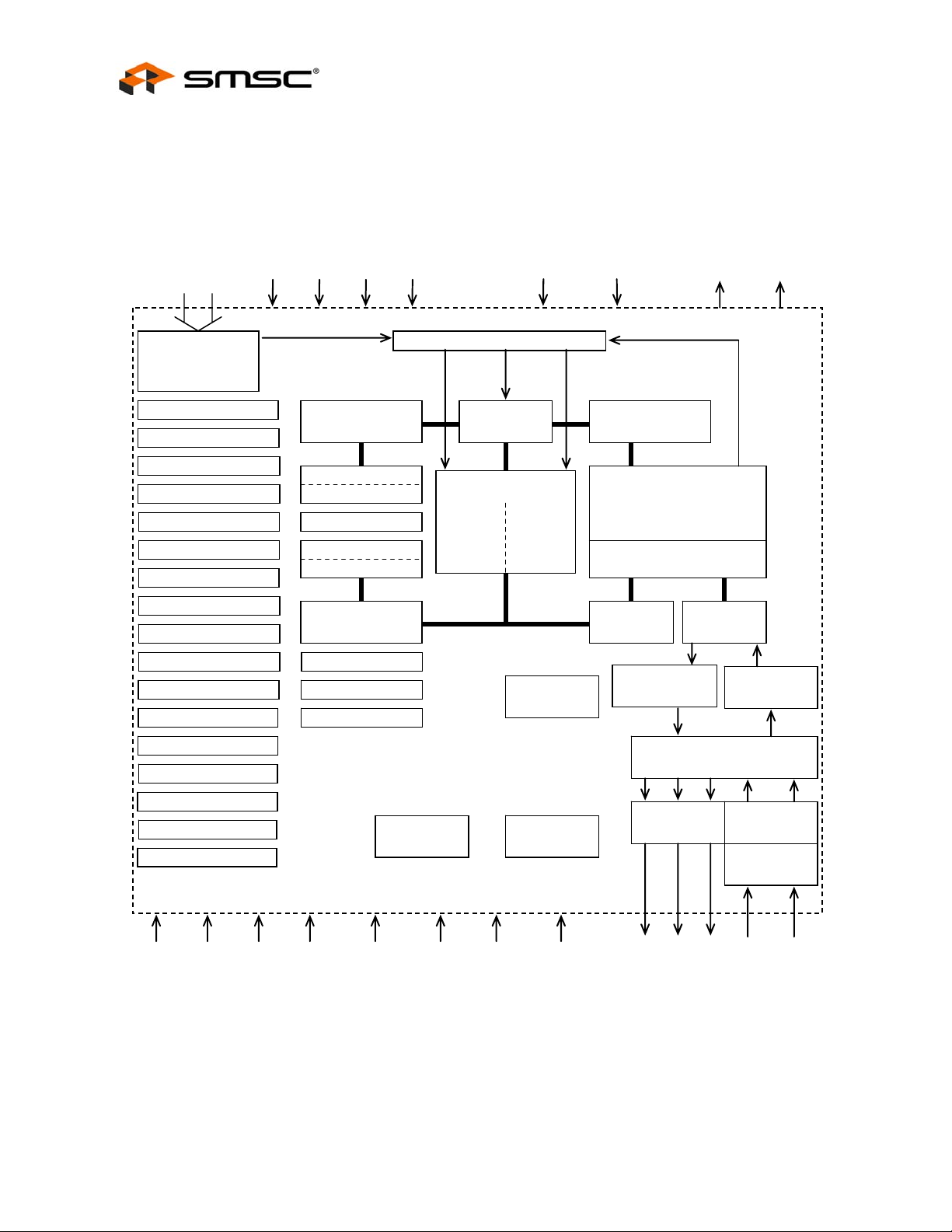
1.2 About the TMC2072
The TMC2072 network controller is CircLink technology’s flagship product. The TMC2072’s flexibility and
rich feature set enable a high-reliability and high-performance, real-time and control-oriented network
without the cumbersome middle layer protocol stacks and complex packet prioritization schemes typically
required.
TMC2072 operates at network data transfer rates up to 5 Mbps. Its embedded 1k Byte RAM can be
configured into a maximum of 32 pages to implement a 31-node network where each node in the network
has the same local memory.
TMC2072 supports “Peripheral Mode” operation, which includes two selectable communication modes:
“Free Format Mode” and “Remote Buffer Mode”. Free Format mode, retained from ARCNET, is “packet
oriented” communication. Remote Buffer mode communication is a CircLink-specific feature, and is a
token oriented communication, which includes automatic data transmission when the token arrives.
The TMC2072 has a flexible 8-bit or 16-bit data bus to interface various CPU types including X86, 68XX,
and SHx with multiplexed or non-multiplexed address/data. When operating in Peripheral mode, the
TMC2072 has 8-bit programmable I/O available. When operating in Standalone mode, the TMC2072’s I/O
configuration is16-bit. The TMC2072 also integrates a 3-port hub (two ports for external connection) to
accommodate various network topologies (Bus, Star, etc.) and combinations.
SMSC TMC2072 Page 7 Revision 0.1 (06-07-07)
DATASHEET
Peripheral Mode CircLink™ Controller
Datasheet
Micro-Controller bus
Register Ac cess
Control Circuit
Mode Setting
Interrupt Sta tu s
Interrupt Mask
EC Command
Receive Mode(#01-#31)
Receive Flag(#01-#31)
Clock Master SID
Net. Standard Time
Alarm Setting
Receive SID
Search SID
MAX ID Setting (MAXID)
nMUX nRWM W16 nSWAP
Memory Access Mediation Circuit
Address pointer
Page Register
Address Register
Diag. Register
Data Register H
Data Register L
Data Latch
TENT-ID Register
CONFIG Register
SETUP Registers
Others
Address
Multiplexer
Buffer Memory
512B 512B
RECON Timer
Clock
Address Pointer
Improved ARCNET Protocol
Micro Sequencer
Working Registers
Data Latch Shift Register
TX Signal
Generator
RX Synchronous
FLASHO nNSTCOUT
circuit
Node ID Setting (NID)
Page Size Setting (PS)
Data Rate Setting
PIN-INFO
ERR-INFO
MAXID NID PS CKP
Reset Circuit
nSTALONE nDIAG
OSC
nHUBON nCMIBYP
TXEN2 RXIN2
3Port HUB Circuit
CMI Decode CMI Encode
CMI Synchro
TXEN TXD RXIN
Figure 1 - TMC2072 Internal Block Diagram
Revision 0.1 (06-07-07) Page 8 SMSC TMC2072
DATASHEET
Peripheral Mode CircLink™ Controller
Datasheet
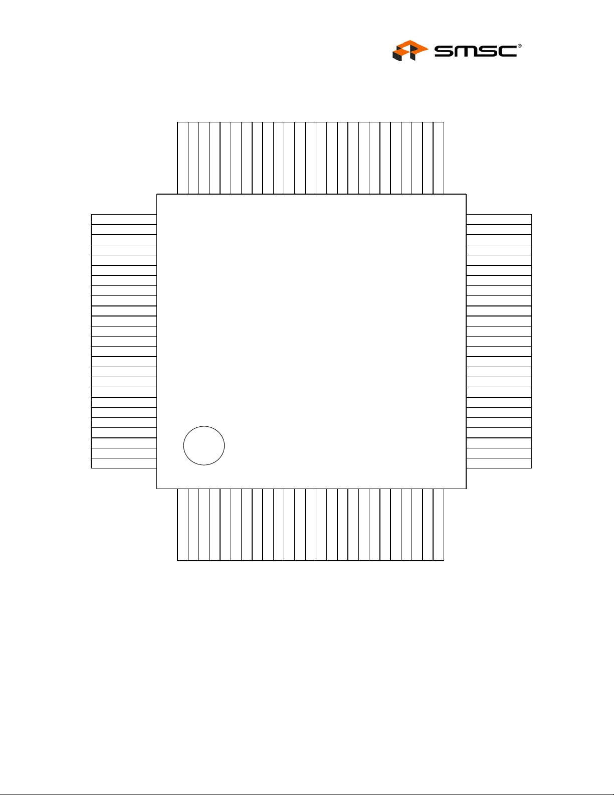
1.3 Pin Configuration
GPIO7
GPIO6
GPIO5
GPIO4
GPIO3
GPIO2
GPIO1
75 74 73 72 71 70 69 68 67 66 65 64 63 62 61 60 59 58 57 56 55 54 53 52 51
GPIO0
*2 *3 *3 *1 *3 *2 *1
FLASHO
nNSTCOUT
VSSX2X1
VDD
MCKIN
VSS
CKP2
CKP1
CKP0
MAXID4
MAXID3
MAXID2
VDD
MAXID1
MAXID0
WPRE0 NID4
WPRE1 NID3
*1
VDD NID2
nTEST0 NID1
nTEST1 NID0
nTEST2 PS1
nTEST3 PS0
(High) NSTPRE1
nEHRD NSTPRE0
nEHWR VDD
*1
VDD VSS
nCMIBYP nDIAG
nOPMD RXIN2
nHUBON ET1
*2
VSS RXIN
NSTPRE2 TXENPOL
nMUX TXEN2
nRWM TXD
W16 TXEN
nSWAP
nCS VSS
A0 nRESET
A1 VDD
A2 (ALE) D15
*2
VSS D14
76
77
78
79
80
81
82
83
84
85
86
87
88
89
90
91
92
93
94
95
96
97
98
99
100
12345678910111213141516171819202122232425
A3 (ALEPOL) / PO3A4VDDA5nDSINV
nRD (nDS)
nTMODE
nWR (DIR)
VDD
D0 (AD0)
D1 (AD1)
D2 (AD2)
D3 (AD3)
VSS
VSS
D4 (AD4)
D5 (AD5)D6D7D8D9
50
49
48
47
46
45
44
43
42
41
40
39
38
37
36
35
34
33
32
31
nINTR
30
29
28
27
26
D10
D11
D12
D13
*1
*2
*2
*4
*1
*1 *1 *2 *2 *1
Power Supply (VDD)
Power Supply (VSS)
*2
Clock Signal
*3
Reset Signal
*4
Figure 2 - TMC2072 Pin Configuration
SMSC TMC2072 Page 9 Revision 0.1 (06-07-07)
DATASHEET

Peripheral Mode CircLink™ Controller
Datasheet
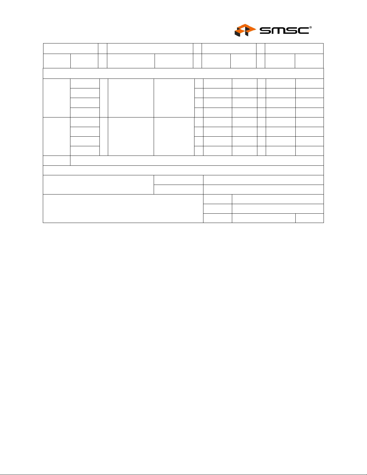
Table 1 - Pin Description
PIN
COUNT PIN NO.
CPU Interface
1
2
3
4
5
6
7
8
9
10
11
12
13
14
15
16
17
18
19
20
21
22
23
24
25
26
27
29
96
97
98
99
1
2
4
6
8
10
11
12
13
16
17
18
19
20
21
22
23
24
25
26
27
31
Total 27
PERIPHERAL MODE
INPUT BUFFER
OUTPUT BUFFER
PULL-
PIN NAME DIRECTION
UP TYPE DRIVE TYPE
nRESET IN Internal T-NRM --- -- nCS IN Internal T-NRM --- -- A0 IN Internal T-NRM --- -- A1 IN Internal T-NRM --- -- A2/ALE IN Internal T-NRM --- -- A3/ALEPOL IN Internal T-NRM --- -- A4 IN Internal T-NRM --- -- A5 IN Internal T-NRM --- -- nRD/nDS IN Internal T-NRM --- -- nWR/DIR IN Internal T-NRM --- -- D0/AD0 BI Internal T-NRM 4mA
D1/AD1 BI Internal T-NRM 4mA
D2/AD2 BI Internal T-NRM 4mA
D3/AD3 BI Internal T-NRM 4mA
D4/AD4 BI Internal T-NRM 4mA
D5/AD5 BI Internal T-NRM 4mA
D6 BI Internal T-NRM 4mA
D7 BI Internal T-NRM 4mA
D8 BI Internal T-NRM 4mA
D9 BI Internal T-NRM 4mA
D10 BI Internal T-NRM 4mA
D11 BI Internal T-NRM 4mA
D12 BI Internal T-NRM 4mA
D13 BI Internal T-NRM 4mA
D14 BI Internal T-NRM 4mA
D15 BI Internal T-NRM 4mA
nINTR OUT --- --- 2mA
Revision 0.1 (06-07-07) Page 10 SMSC TMC2072
DATASHEET

Peripheral Mode CircLink™ Controller
Datasheet
PIN
COUNT PIN NO.
Transceiver Interface
1
2
3
4
5
36
32
33
38
34
Total 5
Clock
1
2
3
63
64
61
Total 3
Setting Pins
1
2
3
4
5
6
7
8
9
10
11
12
13
14
15
16
17
18
19
20
21
22
23
92
93
94
95
42
43
91
44
45
46
47
48
49
50
51
52
54
55
56
57
58
59
39
PERIPHERAL MODE
INPUT BUFFER
OUTPUT BUFFER
PULL-
PIN NAME DIRECTION
UP TYPE DRIVE TYPE
RXIN IN Internal T-NRM --- -- TXEN OUT --- --- 4mA
TXD OUT --- --- 4mA
RXIN2 IN Internal T-NRM --- -- TXEN2 OUT --- --- 4mA
X1 IN --- --- --- --X2 OUT
--- --- --- ---
MCKIN IN Internal T-NRM --- ---
nMUX IN Internal T-NRM --- -- nRWM IN Internal T-NRM --- -- W16 IN Internal T-NRM --- -- nSWAP IN Internal T-NRM --- -- NSTPRE0 IN Internal T-NRM --- -- NSTPRE1 IN Internal T-NRM --- -- NSTPRE2 IN Internal T-NRM --- -- PS0 IN Internal T-NRM --- -- PS1 IN Internal T-NRM --- -- NID0 IN Internal T-NRM --- -- NID1 IN Internal T-NRM --- -- NID2 IN Internal T-NRM --- -- NID3 IN Internal T-NRM --- -- NID4 IN Internal T-NRM --- -- MAXID0 IN Internal T-NRM --- -- MAXID1 IN Internal T-NRM --- -- MAXID2 IN Internal T-NRM --- -- MAXID3 IN Internal T-NRM --- -- MAXID4 IN Internal T-NRM --- -- CKP0 IN Internal T-NRM --- -- CKP1 IN Internal T-NRM --- -- CKP2 IN Internal T-NRM --- -- nDIAG IN Internal T-NRM --- ---
SMSC TMC2072 Page 11 Revision 0.1 (06-07-07)
DATASHEET

Peripheral Mode CircLink™ Controller
Datasheet
PIN
COUNT PIN NO.
24
25
26
27
28
29
30
31
32
33
34
35
76
77
83
84
85
5
87
89
88
37
Total 34
Output Pins
1
2
3
4
5
6
7
8
9
10
66
67
68
69
70
71
72
73
74
75
Total 10
Test Pins
PERIPHERAL MODE
INPUT BUFFER
OUTPUT BUFFER
PULL-
PIN NAME DIRECTION
UP TYPE DRIVE TYPE
TXENPOL IN Internal T-NRM --- -- WPRE0 IN Internal T-NRM --- -- WPRE1 IN Internal T-NRM --- -- Un-USE(High) IN Internal T-NRM --- -- nEHRD IN Internal T-NRM --- -- nEHWR IN Internal T-NRM --- -- nDSINV IN Internal T-NRM --- -- nCMIBYP IN Internal T-NRM --- -- nHUBON IN Internal T-NRM --- -- nOPMD IN Internal T-NRM --- -- ET1 IN Internal T-NRM --- ---
nNSTCOUT OUT --- --- 4mA
FLASHO 3s.O --- --- 4mA
GPIO0 3s.O Internal T-NRM 4mA
GPIO1 3s.O Internal T-NRM 4mA
GPIO2 3s.O Internal T-NRM 4mA
GPIO3 3s.O Internal T-NRM 4mA
GPIO4 3s.O Internal T-NRM 4mA
GPIO5 3s.O Internal T-NRM 4mA
GPIO6 3s.O Internal T-NRM 4mA
GPIO7 3s.O Internal T-NRM 4mA
1
2
3
4
5
79
80
81
82
7
nTEST0 IN Nothing T-NRM --- -- nTEST1 IN Nothing T-NRM --- -- nTEST2 IN Nothing T-NRM --- -- nTEST3 IN Nothing T-NRM --- -- nTMODE IN Internal T-NRM --- ---
Total 5
Revision 0.1 (06-07-07) Page 12 SMSC TMC2072
DATASHEET
Peripheral Mode CircLink™ Controller
Datasheet
PIN
COUNT PIN NO.
Power Pins
3, 9,
1-8
9-16
Total 16
Total Pin = 100
28, 41,
53, 62,
78, 86
14, 15,
30, 40,
60, 65,
90, 100
PIN NAME DIRECTION
VDD PWR
PERIPHERAL MODE
VSS PWR
(High) : Connect to VDD
(Open) : Not connected
INPUT BUFFER
PULL-
UP TYPE DRIVE TYPE
--- --- --- ---
--- --- --- ---
--- --- --- ---
--- --- --- ---
--- --- --- ---
--- --- --- ---
--- --- --- ---
--- --- --- ---
T-NRM TTL Level Input w/o Schmitt
3s/O Tri-state Output or Normal Output
3s.O Tri-state Output
OUTPUT BUFFER
SMSC TMC2072 Page 13 Revision 0.1 (06-07-07)
DATASHEET

1.4 Pin Description by Functions
NOTE: * A pin name starting with “n” indicates an active-low pin.
1.4.1 CPU Interface (27)
D[15:6]/ Data Bus (bit15-6)
D[5:0]/AD[5:0] Data Bus / Address Data Bus (bit5-0)
nCS Chip Select Input
nWR/DIR Write Signal Input / Access Direction
nRD/nDS Read Signal Input / Data strobe
A[5:4] Address Input
A[3]/ALEPOL Address Input / ALE Designate Polarity
Peripheral Mode CircLink™ Controller
Datasheet
A[2]/ALE Address Input / ALE
A[1:0] Address (bit1-0)
nINTR Interrupt Output (Active Low)
nRESET Reset Input (Active Low)
1.4.2 Transceiver Interface (5)
RXIN Port1 Receive Data Input
TXEN Port1 Transmit Enable Output
TXD Transmit Data Output (Port1, 2 Common)
RXIN2 Port2 Receive Data Input
TXEN2 Port2 Tr ansmit Enable Output
1.4.3 Setup Pin (33)
nMUX Select Address Multiplex Mode
nRWM Select R/W Mode
W16 Select Data Bus Width
nSWAP Select Swap Mode
Revision 0.1 (06-07-07) Page 14 SMSC TMC2072
DATASHEET

Peripheral Mode CircLink™ Controller
Datasheet
nDSINV nDS Designate Polarity
PS[1:0] Determine Page Size (*1)
NID[4:0] Determine MyID Number (*1)
MAXID[4:0] Determine MAXID Number (*1)
CKP[2:0] Determine Data Rate (*1)
NSTPRE[2:0] NST Resolution
WPRE[1:0] Select Warning Timer Resolution
nDIAG Select Diagnostics Mode
ET1 Determine ARCNET Extended Timer (*1)
nEHWR Select Enhanced Write Mode
nEHRD Select Enhanced Read Mode
TXENPOL TXEN,TXEN2 Designate Polarity
nOPMD Select Optical Transceiver Mode
nCMIBYP Bypass CMI Modem
nHUBON ON/OFF Determine of Internal HUB function
NOTE: (*1) Could be also determined by the register at the Peripheral Mode
1.4.4 External Output or Input/output (10)
nNSTCOUT NST Carry Output
FLASHO Outside Output for FLASH
GPIO[7:0] General-purpose I/O port (bit7-0)
1.4.5 Other Input (5)
nTEST[3:0] Test Pins
nTMODE Test Mode
SMSC TMC2072 Page 15 Revision 0.1 (06-07-07)
DATASHEET
1.4.6 Clock (3)
X1 Crystal Oscillator
X2 Crystal Oscillator
MCKIN Master Clock Input
X1
Peripheral Mode CircLink™ Controller
Datasheet
X2
MCKIN
- Using an external clock :
X1 is connected to GND with MCKIN connected to the input of the external clock
- Using XTAL :
MCKIN is connected to VDD with X1, X2 connected to the Crystal Oscillator
1.5 User Setup Pins
Setup pins are strapped high or low to configure options according to system design. For low, strap to
ground. Many pins have internal pullups on their input buffers. These pins can be left unconnected to keep
them in high state.
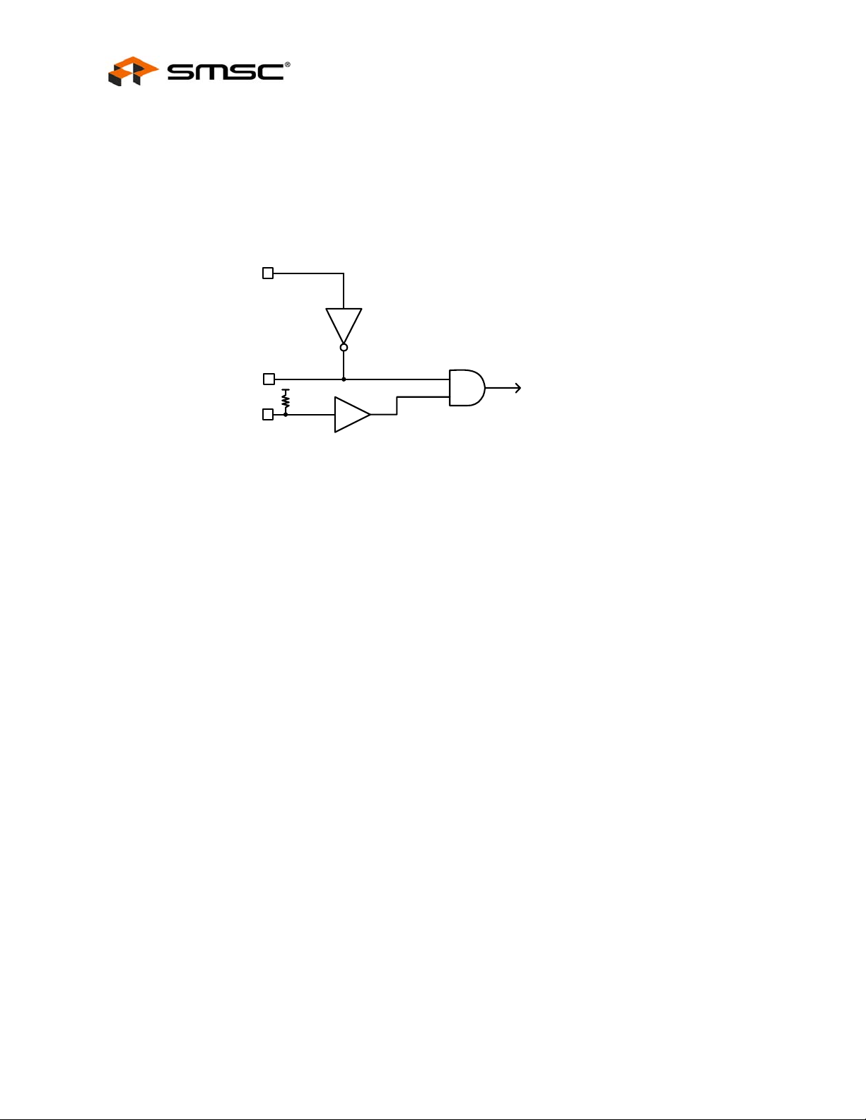
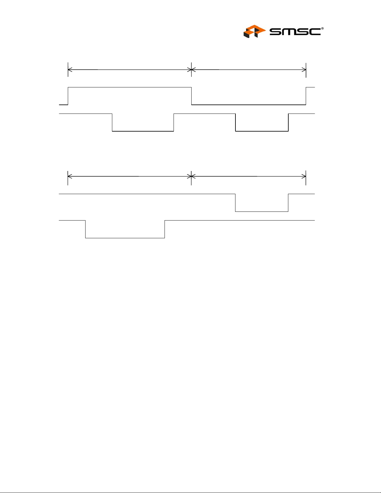
1.5.1 CPU Type Selection
(nRWM: Pin)
MCK
(Internal MasterClock)
In Peripheral mode, this pin selects the CPU type; in this case, the definition of nWR/DIR (pin) and
nRD/nDS (pin) are selected. (Refer to Figure 3 - MOTOROLA CPU Mode (68hXX) and Figure 4 - INTEL
CPU MODE (86XX).
Revision 0.1 (06-07-07) Page 16 SMSC TMC2072
DATASHEET
Peripheral Mode CircLink™ Controller
Datasheet
[nRWM=H, nDSINV=H]
DIR
nDS
nWR
nRD
Read Cycle
Figure 3 - MOTOROLA CPU Mode (68hXX)
[nRWM=L, nDSINV=L or H]
Read Cycle
Figure 4 - INTEL CPU MODE (86XX)
Write C ycle
Write Cycle
1.5.2 Address Multiplex Selection
(nMUX: Pin)
In Peripheral mode, this pin specifies the system data bus from bit 5 to 0 and whether the addresses are
multiplexed (Refer to Figure 5 - Non-multiplex Bus, Figure 6 - Multiplex (ALE falling-edge Type) and Figure
7 - Multiplex (ALE rising-edge Type). When the multiplexing bus option is selected, the polarity of A2/ALE
is specified based on A3/ALEPOL.
SMSC TMC2072 Page 17 Revision 0.1 (06-07-07)
DATASHEET
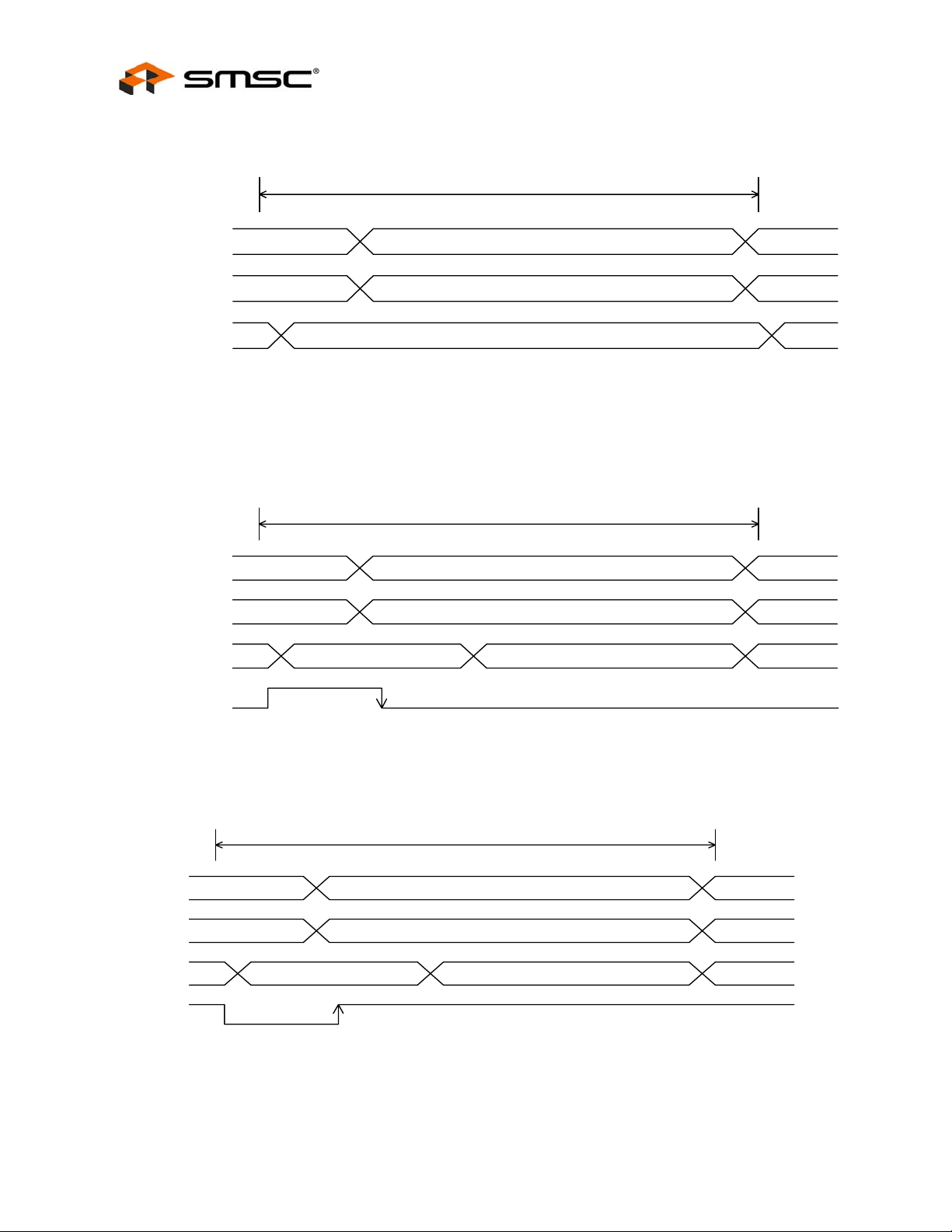
[In case of nMUX=H]
Peripheral Mode CircLink™ Controller
Datasheet
D15-8
D7-0
A5-0
Figure 5 - Non-multiplex Bus
[In Case of nMUX=L, ALEPOL=H]
D ata High B yte
D ata L o w By te
Address
1 Bus C ycle
D15-8
D7-6
AD5-0
Address
Data High Byte
D a ta bit7- 6
D a ta b it5 - 0
ALE
Figure 6 - Multiplex (ALE falling-edge Type)
[In case of nMUX=L, ALEPOL=L]
1 Bus C ycle
D15-8
D7-6
AD5-0
ALE
Address
Figure 7 - Multiplex (ALE rising-edge Type)
Revision 0.1 (06-07-07) Page 18 SMSC TMC2072
D a ta High Byte
D a ta b it7 - 6
D a ta b it5 - 0
DATASHEET
Peripheral Mode CircLink™ Controller
Datasheet
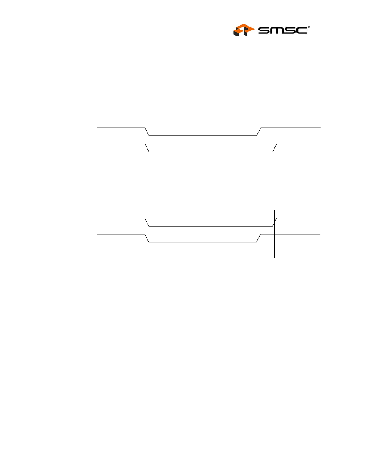
1.5.3 Write Timing Selection
(nEHWR: Pin)
In Peripheral mode, this pin selects the write timing.
[ Example: nMUX=H,nEHWR=H ]
nCS
Write Signal
Tie to Hi for CPU’s where nCS goes Hi before the write signal goes Hi.
[ Example: nMUX=H,nEHWR=L ]
nCS
Write Signal
Tie to Low for CPUs where nCS goes Hi after the write signal goes Hi.
The write signal differs depending on the CPU types.
nRWM = H: nDS signal at DIR = L
nRWM = L: nWR signal
NOTE: Refer to the AC timing specifications (in another document) for details (setup time, hold time, etc.).
Compare timing specifications for nEHWR=L and nEHWR=H.
SMSC TMC2072 Page 19 Revision 0.1 (06-07-07)
DATASHEET
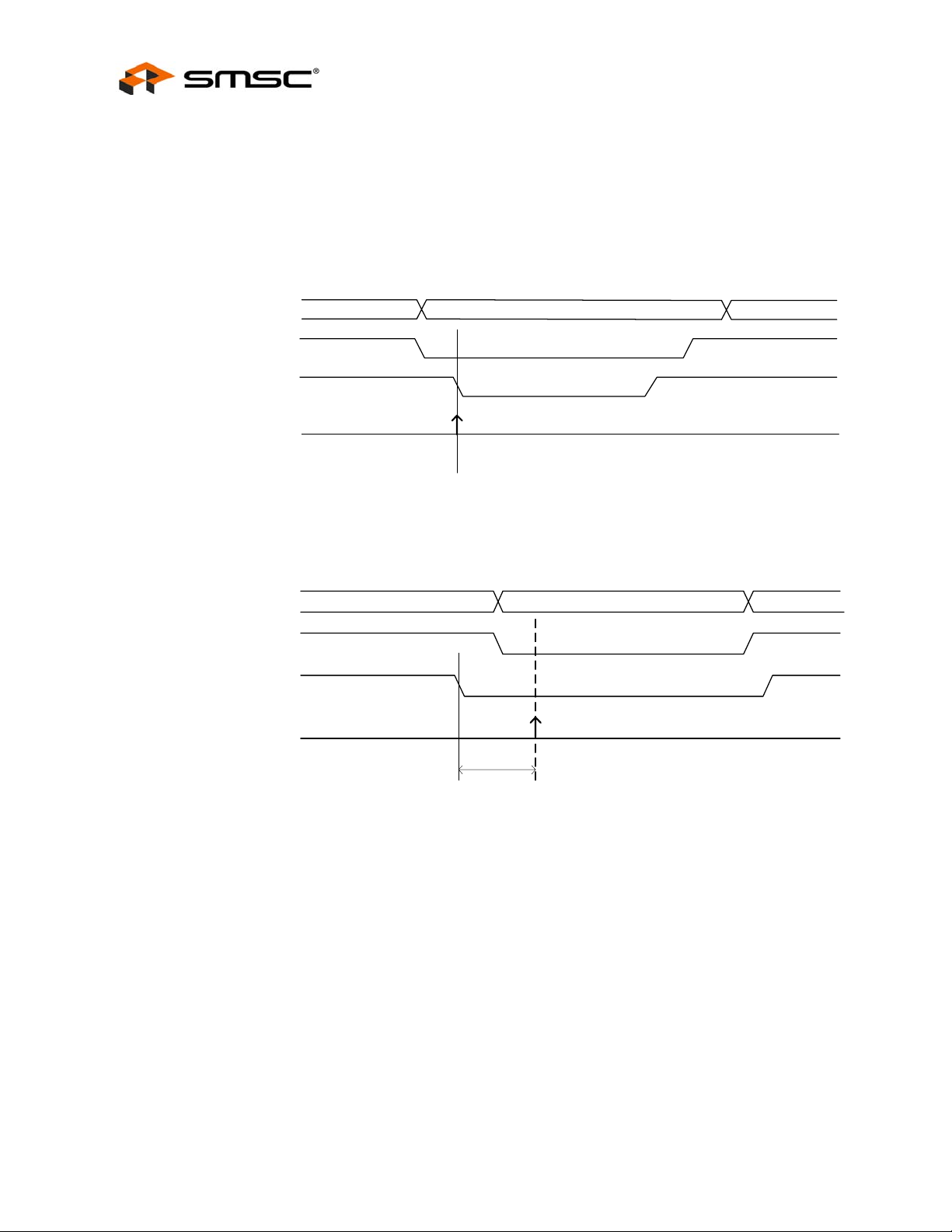
1.5.4 Read Timing Selection
(nEHRD: Pin)
In Peripheral mode, this pin selects the read timing type.
[ In case of nMUX=H,nEHRD=H ]
A[5:0]
nCS
Read Signal
Address Samplin g
timing
Tie to Hi for CPUs with valid address before nCS and the read signal go low.
Peripheral Mode CircLink™ Controller
Datasheet
[ Example: nMUX = H and nEHRD = L ]
A[5:0]
nCS
Read Signal
Address Sampling
timing
Tie to L for the CPU’s where nCS is enabled and addresses are valid after the read signal goes low.
NOTE: Address acquisition timing in the CircLink delays about 50 ns (with 20 MHz-XTAL).
The read signal differs depending on the CPU type:
nRWM = H: nDS signal at DIR = H
nRWM = L: nRD signal
NOTE: Refer to the AC timing specifications (in another document) for details (setup time, hold time, etc.).
Compare timing specifications for nEHRD=L and nEHRD=H.
Revision 0.1 (06-07-07) Page 20 SMSC TMC2072
DATASHEET

Peripheral Mode CircLink™ Controller
Datasheet
1.5.5 Data Bus Width Selection
(W16: Pin)
This pin selects the bit width of the data bus in Peripheral mode; H: 16-bit mode, L: 8-bit mode. In the 16bit mode, the LSB address in the CircLink is fixed to 0.
1.5.6 Data Bus Byte Swap
(nSWAP: Pin)
In Peripheral mode, this pin selects the data order at 8-bit access. CircLink registers are defined as 16-bit
width, but 8-bit access is available and in this case the assignment of lower/upper byte of registers and
odd/even numbers of the address can be changed. nSWAP=L assigns the lower byte to even number
address and the upper byte to odd number address, and nSWAP=H assigns the lower byte to odd number
address and the upper byte to even number address.
1.5.7 Data Strobe Polarity Specification
(nDSINV: pin)
In Peripheral mode, this pin selects the pin polarity of data strobe (nDS). It is active low with nDSINV = H
and active high with nDSINV = L.
1.5.8 Page Size Selection
(PS[1:0]: Pin/Register)
Selects page size per packet. The maximum number of nodes depends on the page size selection since
the packet buffer size is limited to 1 kBytes. There are two methods to specify the page size: either through
pin or register settings depending on INIMODE (bit 9); 0: selects pin, 1: selects register (The default is 0).
PS[1:0] Page Size Max Node Number
00 256 Byte 3 Node
01 128 Byte 7 Node
10 64 Byte 15 Node
11 32 Byte 31 Node
1.5.9 MAXID Number Setup
(MAXID[4:0]: Pin/Register)
The maximum node ID is set based on the number of nodes on the network. All nodes in a CircLink
network, therefore, should have the same maximum node ID. This optimizes the time required to
reconfigure the network. There are two methods to specify the maximum node ID, Either through pin or
register settings depending on INIMODE (bit 9); 0: selects pin, 1: selects register (The default is 0). If the
nDIAG pin is set to L as the exception, however, the maximum node ID is automatically set to the largest
value. For more details, refer to section 2.10 - Diagnostic Mode.
SMSC TMC2072 Page 21 Revision 0.1 (06-07-07)
DATASHEET

Peripheral Mode CircLink™ Controller
Datasheet
1.5.10 Node ID Setup
(NID[4:0]: Pin/Register)
Sets node ID. A unique number must be assigned to each node in the network in ascending order starting
from ID=01. However, ID = 00 and an ID that is larger than the maximum node ID are not valid. There are
two methods to assign the node ID, either through pin or register, settings depending on INIMODE (bit 7)
0: selects pin, 1: select register (The default is 0).
MAXID[4:0] determines the maximum node ID value. The token will only be passed around the nodes
whose IDs are equal to or less than the maximum ID value. In the CircLink network, a node whose
MAXID[4:0] and NID[4:0] matches is the node initiating the token passing.. Even if this particular node is
absent from the network, the network reconfiguration time is greatly reduced because the network will be
reconfigured only for the nodes with IDs less than MAXID[4:0]. Also, given that the maximum number of
nodes is fixed to 31 in a CircLink network, the original priority time of ARCNET, (255 – ID) x 146 μs* ,
which determines the waiting time for network reconfiguration initiation, is modified to (31-ID) x 146 μs,
greatly reducing reconfiguration time. Refer to section 2.4.2 - Reduction of Network Reconfiguration Time
for more details.
NOTE: * 146 μs is defined under operation at 2.5 Mbps based on the ARCNET protocol. The time is half at 5
Mbps.
1.5.11 NST Resolution Setup
(NSTPRE[2:0]: Pin)
Selects the resolution of the network standard time counter (NST). Refer to section 2.11 - Network
Standard Time (NST) for details.
1.5.12 Standalone Mode Specification (Not supported)
TMC2072 does not support standalone mode.
1.5.13 Warning Timer Resolution
(WPRE[1:0]: Pin]
These pins select the warning timer resolution in Peripheral mode. Refer to section 2.9.4 - Warning Timer
(WT) at Remote Buffer Receive for more details.
1.5.14 Diagnosis Mode
(nDIAG: Pin)
This pin sets CircLink to the diagnosis mode. nDIAG to 0 forcibly fixes the MAXID to “1Fh”. Refer to
section 2.10 - Diagnostic Mode for details.
Revision 0.1 (06-07-07) Page 22 SMSC TMC2072
DATASHEET

Peripheral Mode CircLink™ Controller
Datasheet
1.5.15 Prescaler Setup for Communication Speed
(CKP[2:0]: Pin/Register)
CKP2-0 Prescale
40MH z XTA L 20M H z XTAL 32MH z XTA L 16MH z XTA L
Com m unication Speed
000 8 5M bps 2.5Mbps 4Mbps 2Mbps
001 16 2.5Mbps 1.25Mbps 2Mbps 1Mbps
010 32 1.25Mbps 625Kbps 1M bps 500Kbps
011 64 625Kbps 312.5Kbps 500Kbps 250Kbps
100 128 312.5Kbps 156.25Kbps 250Kbps 125Kbps
101 256 156.25Kbps 78.125Kbps 125K bps 62 .5K bps
11 0 res erv ed res erv ed re se rve d res erv ed re s erve d
11 1 res erv ed res erv ed re se rve d res erv ed re s erve d
Communication speed (transfer rate) selection for CircLink. There are two methods to determine the
communication speed, either through pin or register settings, depending on the specification of INIMODE
(bit 9); 0: pin, 1: register (Default is 0).
1.5.16 CPU Interface Bus Timing Selection
(nEHWR, nEHRD: Pin)
For the functions using Peripheral mode, refer to sections 1.5.3 and 1.5.4.
1.5.17 CMI Bypass Specification
(nCMIBYP: Pin)
Selects bypassing the CMI code/encoding. nCMIBYP = L bypasses the CMI coding/decoding circuit so that
encoding is RZ form signal interface, equivalent to the ARCNET back plane mode.
1.5.18 ON/OFF of HUB Function
(nHUBON: Pin)
Selects ON/OFF ; nHUBON=H selects the HUB function OFF, nHUBON=L selects the HUB function ON
and enables the port 2 (RXIN2 and TXEN2) available. ( in nHUBON = H, RXIN2 should be fixed to High.)
Refer to section 2.13 - HUB Function for the detailed operations.
SMSC TMC2072 Page 23 Revision 0.1 (06-07-07)
DATASHEET

1.5.19 Optical Transceiver Mode
(nOPMD: Pin)
Selects the output mode of the sending-enable; nOPMD = H makes the optical transceiver mode
unavailable and allows the TXEN and TXEN2 output pins to function as “sending-enable”. Setting nOPMD
= L allows TXEN and TXEN2 output pins to function as “sending-enable and sending pulse” to be able to
be directly connected to the TTL input pin of the optical transceiver.
1.5.20 TXEN Polarity Select
(TXENPOL: Pin)
Selects the output polarities of the TXEN and TXEN2 signals. TXENPOL = L selects negative logic and
TXENPOL = H selects positive logic.
1.5.21 Extension Timer Setting 1
(ET1: Pin/Register)
Peripheral Mode CircLink™ Controller
Datasheet
Refer to section 2.13 - HUB Function for operational details.
1.5.22 Test Pins
(nTEST[3:0], nTMODE: Pin)
All pins must be connected to VDD.
Revision 0.1 (06-07-07) Page 24 SMSC TMC2072
DATASHEET

Peripheral Mode CircLink™ Controller
Datasheet
Chapter 2 Functional Description
2.1 Communication Specification
- Data transfer bit rate 78.125 kbps to 2.5 Mbps (at 20 MHz Xtal), (5 Mbps at 40-MHz Xtal)
- The max. number of nodes 31 (ID = 00 is not available for user)
- Data transfer check Only the destination node can check data transfer. Other nodes,
however, can receive (monitor) the same data.
- Protocol Enhanced version of ARCNET (token passing)
- Packet size 256 bytes max. (User area: 253 bytes max.)
2.2 Message Class
The following five classes of messages are identical to those in the ARCNET protocol. Refer to the
ARCNET Controller COM20020 Rev. D Datasheet for more details.
ITT (Token)
ALERT EOT
DID
FBE (Free Buffer Enquiries)
ALERT ENQ
DID
ACK (Acknowledgements)
ALERT ACK
NAK (Negative Acknowledgements)
ALERT NAK
PACKET (Data Packets)
ALERT SOH
SID
DID
DID
DID
DID CP CRC CRC
DATA X n
N : MAX253
(ARCNET Layer)
SMSC TMC2072 Page 25 Revision 0.1 (06-07-07)
DATASHEET

Peripheral Mode CircLink™ Controller
2.3 CircLink Network Communication Protocol Overview
CircLink is derived from the ARCNET protocol. This section explains the ARCNET basic communication
protocol.
A token (ITT Invitation to Transmit) is a unique signaling sequence that is passed in an orderly fashion
among all the active nodes in the network. When a particular node receives the token, it has the sole right
to initiate a transmission sequence or it must pass the token to it’s logical neighbor. This neighbor can be
physically located anywhere on the network and has the 2nd highest address. Once the token is passed to
the recipient, it has the right to initiate transmission. This token-passing sequence continues in a logical
ring fashion serving all nodes equally. Node addresses must be unique and can range from 0 – 255 with 0
reserved for broadcast messages. In a transmission sequence the node with the token becomes the
source node and any other node selected becomes the destination node. First the source node inquires if
the destination node is in a mode to receive a transmission by sending out a free buffer enquiry (FBE). The
destination node responds by returning an Acknowledgement (ACK) meaning that the buffer is available or
by returning a negative Acknowledgement (NAK) meaning that no buffer is available. Upon receiving the
ACK, the source node sends out the data transmission (PAC) with either 0 – 507 bytes of data (PAC). If
the data was properly received by the destination node as evidenced by a successful CRC test, the
destination node sends another ACK. If the transmission was unsuccessful, the destination node does
nothing causing the source node to timeout. The source node will therefore, infer that the transmission
failed and will retry after it receives the token on the next token pass. The transmission sequence
terminates and the token is passed to the next node. If the desired message exceeds 507 bytes the
message is sent in a series of packets-one packet every token pass.
Datasheet
The ARCNET protocol comprises the reconfiguration process to ensure the complete token passing for
every node linked to the network.
ARCNET has the ability to reconfigure the network automatically if a node is either added or removed from
the network. If a node joins the network it does not automatically participate in the token passing
sequence. Being excluded from receiving the token the new node will generate a reconfiguration burst that
destroys the token passing sequence. Once the token is lost all nodes will cease transmitting and begin a
timeout sequence (Priority Timer, (255-ID) x 146 μs , based on their own node address. The node (Node
ID=N) with the highest address will timeout first and pass the token to the next higher address (Node
ID=N+1).. If that node does not respond, it is assumed that node does not exist. Then the destination node
address is incremented (Node ID=N+2) and the token resent. This process is repeated until a node
responds. At that time the token is released to the responding node and the address of the responding
node is noted as the logical neighbor of the originating node. This process is repeated by all nodes until
each node learns its logical neighbor. This eliminates wasting time in sending datagrams to absent
addresses once the network has been re-established.
When a node leaves the network the reconfiguration process is slightly different. When a node releases
the token to its logical neighbor, it expects its logical neighbor will respond within the respond timeout
window (78 μs) either a token pass or the start of a transmission sequence. If no response within the
response time out window, it assumes that its neighbor has left the network and immediately begins a
search for a new logical neighbor by incrementing the node address of its logical neighbor and initiating a
token pass. Network activity is again monitored and the increment process and resending of the token
continues until a new logical neighbor is found. Once found the network returns to the normal logical ring
routine of passing token to logical neighbors.
These reconfiguration sequences of the network are automatic and seamless without software intervention
required.
Revision 0.1 (06-07-07) Page 26 SMSC TMC2072
DATASHEET

Peripheral Mode CircLink™ Controller
Datasheet
2.4 CircLink Protocol Enhancement
Since the communication of ARCNET is controlled by a token, a token loss and the corresponding
reconfiguration significantly reduce the throughput of the network. In order to maintain the throughput,
modification of the ARCNET protocol is required to realize even higher real-time performance.
2.4.1 Reducing Token Loss
The primary source of token loss is caused by the burst signal. The burst signal is part of the sequence for
new nodes joining the network as described in section 2.3. In the CircLink, however, any new nodes do not
join because all nodes join to the network at the system start-up. In exceptional cases, the node leaves the
network due to token loss and a burst signal sent to r re-join the network. In order to avoid this burst signal,
the ARCNET protocol has been modified to specify node IDs as consecutive numbers starting from 01.
When a node other than the node having the largest node ID (NID [4:0] and MAXID[4:0]) sends a token
with the starting address being the node ID +1, this avoids sending a burst because a token can be
received in the next polling, even if a node has accidentally dropped out from the network.
The token retry function has been added to CircLink such that the possibility of not receiving the response
from the logical neighbor is greatly reduced due to token corruption . . Since the node ID in the CircLink is
consecutive and the retry does not occur in normal conditions, the token retry function does not degrade
the total performance. This function can be set to ON or OFF using software settings. (The default is ON)
Another cause of the token loss is the corruption of ACK/NAK. In the ARCNET flow (refer to page 12 in the
ARCNET controller COM20020I datasheet), if the node receives other signals other than the anticipated
ACK/NAK response (such as noise or, data-deformed ACK/NAK and the like), this node returns to the
receive-wait state with a token being held by the node. The network considers this as a token loss because
the token disappears from the network. To avoid this problem, ARCNET protocol has been modified to
send a token even after the detection of ACK/NAK corruption This function against the ACK/NAK
deformation can be set to ON or OFF. (The default is ON.)
2.4.2 Reduction of Network Reconfiguration Time
To reduce the waiting duration of (255 - ID) x 146 μs* during the network reconfiguration time, CircLink
designates a the node with the maximum ID as the maximum node (MAX_NODE). The node designated to
the maximum node immediately starts sending a token. The destination number starts from 00. The token
sending to 00 is not received by any node but triggers the other nodes to enter into the receive state out of
the (255 - ID) x 146 μs* timer. In addition, the 255 of (255 - ID) x 146 μs* timer formula, derived from
ARCNET, the is modified to
(The maximum number of nodes –ID) x 146 μs depending on the maximum number of nodes, which is
specified by the MAXID [4:0] pin. This modification makes significant reduction of the time required for
network reconfiguration even in the absence of the node set as MAX_NODE.
NOTE: * 146 μs is the time under operation at 2.5 Mbps. The time is half at 5 Mbps..
SMSC TMC2072 Page 27 Revision 0.1 (06-07-07)
DATASHEET
Peripheral Mode CircLink™ Controller
A
Datasheet
2.4.3 Reduction of Reconfiguration Burst Signal Send Time.
Since the CircLink maximum packet size is smaller than for ARCNET, the reconfiguration burst signal is of
shorter duration, reducing the time required for network reconfiguration as listed in the table below:
CircLink
PS[1:0] MAX Packet Size Burst Signal Sending Time
00 256(253)Byte 1.63ms
01 128(125)Byte 1.07ms
10 64(61)Byte 0.79ms
11 32(29)Byte 0.65ms
RCNET
-- MAX Packet Size Burst Signal Sending Time
-- 512(508)Byte 2.75ms
() : Data Size
NOTE: Above “Burst Signal Sending Time” is the time for operation at 2.5 Mbps. The time is half at 5 Mbps.
2.5 RAM Page Expansion
The original ARCNET buffer RAM is divided into 256 or 512-byte per a page. This configuration has a
maximum of four pages available in 1 kByte increments, leaving the majority of the RAM unused when
small data packets are used The CircLink RAM addressing has been modified to significantly expand the
available RAM page numbers and to store pages corresponding to the node IDs on the network as listed in
the table below.
Table 2 - Number of Nodes and RAM Page Size
PAGE SIZE PS[1:0] NODE ID (MIN)
256 Byte 00 01h 03h 100h X ID
128 Byte 01 01h 07h 80h X ID
64 Byte 10 01h 0Fh 40h X ID
32 Byte 11 01h 1Fh 20h X ID
NOTE: *1 : Node ID = 00 is used only for the system development and is not available for users.
*1
NODE ID(MAX) PAGE ADDRESS
Revision 0.1 (06-07-07) Page 28 SMSC TMC2072
DATASHEET
Peripheral Mode CircLink™ Controller
.
Datasheet
2.5.1 RAM Access
The CPU accesses the packet buffer (RAM) through the COMR4 register. Prior to access, a read or write
and page number need to be specified using the COMR2 register, as well as the address specification in
the page using the COMR3 register. The accessing method varies depending on the bit width of data bus,
word mode, and swap mode.
(1) Data bus = 16bits (W16 pin=H)
COMR2 Register : RDDATA, AUTOINC, nWRAPAR, PAGE[4;0]
A/AD[5:0] = 04h - - - - - - - - RD
COMR3 Register : Address Within a page RAMADR[7:0]
A/AD[5:0] = 06h - - - - - - - - 7 6 5 4 3 2 1 X
COM4 Register : Packet Data RAMDT[15:0]
A/AD[5:0] = 08h 15 14 13 12 11 10 9 8 7 6 5 4 3 2 1 0
(2-a) Data bus = 8bits , Word mode=OFF
A.I.
W.A43210
Bit0 is fixed in 0 in the inside.
(W16 pin=L, WDMD=0 in MODE REG.)
COMR2 Register : RDDATA AUTOINC nWRAPAR PAGE[4:0]
A/AD[5:0] = 04h (05h) * RD. A.I.
COMR3 Register : Address within a page RAMADR[7:0]
A/AD[5:0] = 06h (07h) * 76543210
COMR4 Register : Packet Data RAMDT[7:0]
A/AD[5:0] = 08h or 09h 76543210
( )*:nSWAP=L
W.A43210
SMSC TMC2072 Page 29 Revision 0.1 (06-07-07)
DATASHEET
(2-b) Data bus = 8bits , Word mode=ON
(W16 pin=L, WDMD=1 in MODE REG.)
COMR2 Register : RDDATA AUTOINC nWRAPAR PAGE[4:0]
Peripheral Mode CircLink™ Controller
Datasheet
A/AD[5:0] = 04h (05h) * RD. A.I.
W.A43210
COMR3 Register : Address within a page RAMADR[7:0]
A/AD[5:0] = 06h (07h) * 7 6 5 4 3 2 1 X
Bit0 is fixed in 0 in the inside.
COMR4 Register : Packet Data RAMDT[15:0]
A/AD[5:0] = 08h (09h) * 7 6 543210
A/AD[5:0] = 09h (08h) * 151413121110 9 8
( )*:nSWAP=L
NOTE: In word mode = ON, to preserve the upper and lower bytes of word data as in the identical packet, COMR4
must be accessed in order of 08h first and 09h second. This restriction applies to both read and write.
Moreover, it is impossible to independently access CP (address = 02h) in RAM independently To access
the CP, a dummy cycle is necessary. Refer to section 2.5.3 - Packet Data Structure for detail.
Revision 0.1 (06-07-07) Page 30 SMSC TMC2072
DATASHEET

Peripheral Mode CircLink™ Controller
Datasheet
2.5.2 Packet Buffer Structure
32 Byte Mode
PAGE[4:0]
64 Byte Mode
128 Byte Mode
1024Byte
32Page
1024 Byte
16Page
#00 (00h)
#01 (01h)
:
#31 (1Fh)
PAGE[3:0]
#0 (0h)
#1 (1h)
:
#15 (Fh)
PAGE[2:0]
RAMADR[4:0]
00h
01h
32Byte
:
1Fh
RAMADR[5:0]
00h
01h
64 Byte
:
3Fh
#0
1024 Byte
8Page
#1
:
#7
256 Byte Mode
1024 Byte
4Page
SMSC TMC2072 Page 31 Revision 0.1 (06-07-07)
PAGE[1:0]
#0
#1
#2
#3
RAMADR[6:0]
00h
01h
128 Byte
:
7Fh
RAMADR[7:0]
00h
01h
256 Byte
:
FFh
DATASHEET

R
2.5.3 Packet Data Structure
PS = [1:0] = Example of 11 (32-byte mode)
8 bit constitution 16 bit constitution
(W16=L,WDMD=0) (W16=L,W DMD=1 OR W16=H)
Peripheral Mode CircLink™ Controller
Datasheet
RAMADR RAMAD
7 0 15 8 7 0
00 SID
01 DID
02 CP = 1A
.
00
02
.
.
1A DATA #0
1B DATA #1
1C DATA #2
1D DATA #3
1E DATA #4
1F DATA #5
SID: Source-ID (Source node ID)
DID: Destination-ID (Destination node ID) : DID=0 means the broadcast packet.
CP: Continuation pointer
Write the value (Page size - N) for sending N-byte data. That is, it indicates the top position of data in the
page. The example shows the value is 1Ah (32 - 6 bytes = 26 bytes = 1Ah).
1A
1C
1E
10
DID
dummy
SID
CP=1A
.
.
DATA #0 DATA #0
( Upper Byte ) ( Lower Byte)
DATA #1 DATA #1
( Upper Byte ) ( Lower Byte)
DATA #2 DATA #2
( Upper Byte ) ( Lower Byte)
NOTES: Limitations on the specifiable values for CP.
32B Mode (PS [1:0] = 11) : Values from 03h to 1Fh
64B Mode (PS [1:0] = 10) : Values from 03h to 3Fh
128B Mode (PS [1:0] = 01) : Values from 03h to 7Fh
256B Mode (PS [1:0] = 00) : Values from 03h to FFh
If a packet is sent with CP other than the specified value the destination node rejects the packet, and the
session closes with a sending error (TXERR). Simultaneously the CP error (CPERR) flag of the EC status
register is set, which can issue an interrupt. The error flag, however, means a setup or CP specification
error to the CircLink, and does not indicate a network error.
Sender:
Sending error (TXERR) and CP error (CPERR) flags are set and a token is passed to the next node. Since
TA flag is reset to 1 except in the remote buffer mode (TXM = 1) as well as the continuous send mode
(RTO = 0), a send command must be issued for re-sending.
Revision 0.1 (06-07-07) Page 32 SMSC TMC2072
DATASHEET

Peripheral Mode CircLink™ Controller
Datasheet
Receiver:
The receiver rejects the packet and goes back to idle state.
2.6 CPU Interface
2.6.1 CPU Identification and Compatibility Between Intel and Motorola
Processors
The CircLink Controller, TMC2072, can be connected to any combination of CPUs listed in the Table 3.
For more information on setup, refer to section 1.5 - User Setup Pins.
Table 3 - CPU Type
CLASSIFICATION ITEM
16 BIT CPU 8 BIT CPU
Address Multiplexed Non-MUX / Multiplexed Non-MUX / Multiplexed
Data Bus width 8bit / 16bit 8bit
Read / Write nRD , nWRL
DIR , nLDS(LDS)
Table 4 describes setup of pin functions of address bus/data, bus/read write controls by nRWM and nMUX
pins.
Table 4- Distinction and Matching of the CPU type
PIN NAME
D15 - D6 D15-D6 D15-D6 D15-D6 D15-D6
D/AD5 - D/AD0 AD5-AD0 D5-D0 AD5-AD0 D5-D0
A5-A4 - A5-A4 - A5-A4
A3 ALEPOL A3 ALEPOL A3
A2 ALE A2 ALE A2
A1-A0 - A1-A0 - A1-A0
nW R /DIR nWR nWR DIR DIR
nR D / n DS nRD nRD nDS(DS) nDS(DS)
INTEL (80XX) TYPE MOTOROLA (68XX) TYPE
NRWM = 0 NRWM=1
NMUX=0 NMUX=1 NMUX=0 NMUX=1
CONNECTION CPU TYPE
OR
nRD , nWR
OR
DIR , nDS(DS)
Remarks:
Symbol definition in Table 4:
D Data Bus
A Address Bus
AD Address / Data Bus
nWR Write Signal (16 Bit CPU is nWRL)
SMSC TMC2072 Page 33 Revision 0.1 (06-07-07)
DATASHEET

Peripheral Mode CircLink™ Controller
nRD Read Signal
DIR Read / Write Signal
nDS(DS) Data Strobe Signal (16 Bit CPU is nLDS) (Polarity is designated by nDSINV pin)
ALE Address Latch Enable Signal
ALEPOL Designate ALE polarity
2.6.2 Interface Restrictions
1) Data Strobe signal using Motorola 16-bit CPU
When executing word (16 bit) access to odd addresses by DIR and data strobe signals, the Motorola CPU does
not discriminate between upper and lower data strobe signals. Because of this, it is necessary to OR the upper
and lower data strobe signals to provide the data strobe input.
Datasheet
2) Note on data send
When transmitting and receiving data of 8 bits and 16 bits, the transmitter node can send odd-numbered bytes
but the receiving node can only implement word access (16-bit), the word is read with one invalid upper data
byte. To use the receive data function in a system, special care must be taken. This problem occurs only when
the CP field value in the packet is an odd number.
Revision 0.1 (06-07-07) Page 34 SMSC TMC2072
DATASHEET

Peripheral Mode CircLink™ Controller
Datasheet
2.7 Operation and Communication Modes of CircLink
TMC2072 supports only Peripheral mode, meaning communications require an external CPU. TMC2072
does not support standalone mode, which enables communications without a CPU.
There are two communication modes in Peripheral mode: Free-format mode which is capable of handling a
free-format packet, and Remote Buffer mode, which uses CircLink as a simple buffer. Register bits RXM01
to 31 specify the RX mode of each page and TXM specifies the mode for TX mode.
Operation Mode Communication Mode
Standalone mode
Note: TMC2072 does not support standalone mode.
Peripheral mode
2.7.1 Operation Mode
Peripheral mode
Receive
Transmit
=0
*1
Receive of Free F ormat Mode
(Every Page every designate)
RXMn
*1: n = 01 to 31
=1
*1
Receive of Remote Buffer Mode
(Every Page every designate)
RXMn
*1: n = 01 to 31
TXM
Transmit of Free Format Mode
=0
TXM
Transmit of Remote Buffer Mode
=1
Peripheral mode acts as the CPU's peripheral circuit and has two communication modes, Free-format
mode and Remote Buffer mode. The communication mode is independently selectable for send and
receive; TXM of the Mode register for sender and RXM01 to RXM31 of the Receive Mode register for
receive. The communication mode for sender and receiver must be identical and the communication mode
of the receiver page should be adjusted to the communication mode of the sender.
SMSC TMC2072 Page 35 Revision 0.1 (06-07-07)
DATASHEET

S
Standalone mode
In Standalone mode CircLink independently executes send and receive sequences without a CPU.
However, TMC2072 can not use standalone mode because it does not support standalone mode.
2.7.2 Communication Mode
Free-format mode
Free format mode is retained from the original ARCNET specification. This mode is not optimal for realtime performance but is useful for transferring large amounts of data at once. CPU controls a series of
sequence such as "Packet preparation → Issuing TX command → Interruption handling after the end of
TX" at sender and "Receive command issuing → Interrupt handling after the end of RX→ Packet read" at
receiver.
Since CircLink initiates the actual TX upon receipt of a token addressed to the node, the time between a
TX command being issued and TX starting varies depending on the line status. The free format mode is a
"packet-oriented" transfer mode that assumes a completion of packet preparation before issuing a TX
CMD, so its real-time performance is not as high as that of the remote buffer mode “token-oriented” mode.
On the other hand, the free format mode has no limitation on the packet data structure, and it can handle
free format packets. Moreover, communications in this mode are initiated only by writing a TX CMD,
thereby reducing traffic on the network.
Peripheral Mode CircLink™ Controller
Datasheet
8 bit constitution 16 bit constitution
(W16= L,WDMD=0) (W16=L,WDMD=1 OR W16=H)
RAM-ADRS RAM-ADR
7 0 15 8 7 0
00 SID
01 DID
02 CP
03
04
05
.Free
.Format
.
.
1E
1F
Figure 8 - Packet Structure of Free Format Mode (Example of 32 bytes/page)
00 DID SID
02 CP
04
.
.
.
.
1E
10
dummy
Free
Format
Revision 0.1 (06-07-07) Page 36 SMSC TMC2072
DATASHEET

Peripheral Mode CircLink™ Controller
S
Datasheet
Remote Buffer Mode
Remote Buffer mode, a CircLink enhancement, optimizes real-time performance. In this mode CircLink can
be handled as a simple data buffer like "write data into the CircLink at any time" at a transmit node and
"read data from the CircLink at any time" at a receiver node “.
Since the remote buffer mode is a "token-oriented" mode that features automatic transmission each time a
node receives a token (= sending right), preparation of the packet header portion (SID, DID, and CP) is
required prior to issuing a TX CMD. The data portion of a packet must be valid in 8 or 16 bits. This mode
restricts the data structure, but it is optimized in its real-time performance when compared to Free Format
mode since it can always communicate with the packet data.
Setting RTO to 1 (Default = 0) in the mode register limits CircLink to one packet per TX CMD write. If RTO
is switched to 1 while operating under RTO = 0, the automatic send operation is disabled immediately after
the completion of the packet delivery.
8 bit constitution 16bit constitution
(W16 = L, WDMD=0) (W16=L,WDMD=1 OR W16=H)
RAM-ADRS RAM-ADR
7 0 15 8 7 0
00 SID
01 DID
02 CP=1A
::
00 DID SID
02 dummy CP=1A
:: :
:: :
1A BYTE#0
1B BYTE#1
1C BYTE#2
1D BYTE#3
1E BYTE#4
1F BYTE#5
1A
1C
1E
( Upper Byte) ( Lower Byte )
( Upper Byte) ( Lower Byte )
( Upper Byte) ( Lower Byte )
Figure 9 - Packet Structure of Remote Buffer Mode (Example of 32 bytes/page)
In 16-bit constitution, upper and lower bytes in the same word are preserved as the same packet data
(Refer to section 3.2.5 - COMR4 Register: Data Register).
10
:
:
WORD#0 WORD#0
WORD#1 WORD#1
WORD#2 WORD#2
SMSC TMC2072 Page 37 Revision 0.1 (06-07-07)
DATASHEET

Peripheral Mode CircLink™ Controller
2.8 Sending in Peripheral Mode
To send data using CircLink, it is necessary to write data being transmitted in the packet buffer regardless
of the communication mode. For TX, the page corresponding to its node ID in the packet buffer is assigned
as the TX buffer. The CPU writes TX data on this page.
2.8.1 Example of Sending Control from CPU in Free Format Mode
(MODE REGISTER: TXM = 0)
The CPU manages all series of communication sequence such as "Packet preparation → Issuing TX CMD
→ Handling interrupt after the end of TX".
(NID=n)
CPU Side TMC2074 /72 LAN Side
1 Write to Packet
2 Transmit Command TA = 1 --> 0
3 Release Interrupt mask
…… …
…… …
Transmit Start Token [DID=n]
(FBE)
(ACK)
PAC
Transmit End (ACK)
TA = 0 --> 1 Token [DID=n+1]
4 Read Status Interrupt occurre
Datasheet
5 Interrupt Mask
( ):
Not executed in the case of broadcast transmit.
NOTE: When DID set to 00h, it becomes the broadcast packet.
Revision 0.1 (06-07-07) Page 38 SMSC TMC2072
DATASHEET

Peripheral Mode CircLink™ Controller
Datasheet
2.8.2 TX Control from CPU in Remote Buffer Mode
(MODE REGISTER: TXM = 1)
CircLink can be treated as a simple data buffer so that the system CPU can write data to the CircLink at
any time.
(NID = n)
CPU Side TMC2074/72 LAN Side
1 Write A ddress
2 Write D a ta
3 Transmit Command TA = 1->0
…… …
…… …
Start T ransmit T oken[DID=n]
(FBE)
PAC
End Transmit (ACK)
Keep of TA = 0 (*1) T oken[DID=n+1]
…… …
4 Write D a ta
4 Write D a ta
4 Write D a ta
…… …
5 repeatedly repeatedly
Au to matic tr an s mit at
ea ch time o f th e rec e ive
of s e lf T ok e n
(AC K )
( ): Not done for broadcasts
NOTE: When DID is set to 00h it becomes the broadcast packet.
(*1)
If the RTO bit is 0 in the mode register, CircLink continues sending packets with a single TX CMD. The TA
bit that represents TX end, continues to be 0 unless RTO is set to 1 (constant TX status).
If the RTO bit is 1, the TA bit returns to 1 after each packet is transmitted, as in Free Format mode. TX
CMD must be issued every time but this does not significantly increase traffic on the network, making it
suitable for applications such as handling sensor information that remains fairly constant.
2.9 Receive in Peripheral Mode
CircLink receives all packet data on the network. After receiving a packet without any errors, CircLink
stores the packets in the relevant page in packet RAM according to the source ID (SID) included in the
packet. Receiving the data packet addressed to the node has four steps: Receiving FBE → Sending ACK
→ Receiving PACKET→ Sending ACK. For receiving a data packet addressed to another node in the
network, the packet is stored in the relevant page without sending an ACK.
As described above, CircLink constantly receives packets, with one exception: It abandons the received
packets when the receive mode of the corresponding page is Free Format mode and the receive flag is set
SMSC TMC2072 Page 39 Revision 0.1 (06-07-07)
DATASHEET

Peripheral Mode CircLink™ Controller
Datasheet
to 1 (Receive Inhibited). In this case, CircLink does not return an ACK even if the packet is addressed to
the node (this case is handled as a receive error).
If the receive mode of the corresponding page is set to Remote Buffer mode, CircLink unconditionally
stores packets in the corresponding page in the packet RAM as long as the received data is valid. The
previous packet is overwritten and the newest packet is always stored in the packet RAM.
The meaning of the receive flag varies depending on the receive mode:
(1) Free format receive mode
0: Receive wait or receiving
1: Receive is inhibited or receives is completed
(2) Remote buffer receive mode
0: No receive in a certain period
1: One or more receive in a certain period
Revision 0.1 (06-07-07) Page 40 SMSC TMC2072
DATASHEET

Peripheral Mode CircLink™ Controller
Datasheet
2.9.1 Temporary Receive and Direct Receive
Packets received are stored in the pages partitioned by the received source ID (received SID). There are
two methods for storing packets: storing after error checking through a temporary buffer (#00), and storing
directly. The decision of which process is used is automatically selected in CircLink based on the
combination of page size and communication speed prescaler setting. The smaller the page size or the
larger the division ratio of the transfer rate prescaler, the more data packets will be received through the
temporary buffer.
Prescale Page Size Setting?PS[1:0]
CKP[2:0]
Bit Rate : Input clock
000 1:8
001 1:16
010 1:32
CKP>=011 1:64 over Omission
O :
%
In the table above, “ % ” indicates ‘Temporary Relay Reception is not available in the default setting.
However, by setting the FARB Bit = 1 in register, Setup 2 temporary relay reception is available. The FARB
Bit = 1 setting is possible when the FARB bit default is 0 and only when the input clock is below 20 MHz.
When the clock exceeds 20 MHz, it should not
during software reset.
In temporary buffer receive mode, the packet data containing any errors is left at page 00 if the receive
terminates abnormally (CRC error, etc.) the copy to "SID page" corresponding to the received source ID
(Receive SID), is not executed (the received data is discarded).
In direct receive mode, the packet data containing errors is left at “SID page” even if the receive terminates
abnormally (CRC error, etc.).
Communicatio n Sp eed 11:32B 10: 64B 01:128B 00:256B
2.5 Mbps : 20 MHz Xtal
1.25 Mbps : 20 MHz Xtal
625 kbps : 20 MHz Xtal
OO%X
OOO
OOOO
OOOO
Receive through temporary buf fer av ailable
Receive through temporary buf fer not availabl e
X :
Receive through temporary buf fer av ailable wit h condition
:
see paragraph below.
be set to 1. Also, FARB Bit renewal must be carried out
%
Regardless of whether the receive is done through temporary buffer or direct receive, the RXF# flag upon
abnormal termination of receive is set to 0 (not completed). It does not matter which receive process is
being used because free format mode assumes that the receive is always checked with the RXF# flag. *
On the contrary, the receive process is important in the remote buffer receive mode with direct receive. *
In the worst case, if SID is corrupted in the received packet, the packet data may be written to the wrong
page.
SMSC TMC2072 Page 41 Revision 0.1 (06-07-07)
1
DATASHEET
2.

Receive Mode R XM [31:01]
Receive structure 0: Free Format 1: Rem ote Buffer
T e m p o ra ry rou tin g re ce ive O O
D irect re ce ive
O *
O : Received data reliable
X: No reliablity of received data
Table 5- Page Format of Packet Buffer
[NID[4:0]=11110, PS[1:0]=11 : 32Byte/Page]
RAM ADDRESS PAGE USAGE
000 – 01F
020 – 03F
:
3A0 – 3BF
3C0 – 3DF
3E0 – 3FF
[NID[4:0]=X1110, PS[1:0]=10 : 64Byte /Page]
#01
#01
:
#29
#30
#31
Temporary buffer for receive
Data from Node01
:
Data from Node29
Buffer for transmit
Data from Node31
1
X *
Peripheral Mode CircLink™ Controller
Datasheet
2
RAM ADDRESS PAGE USAGE
000 - 03F
040 - 07F
:
340 – 37F
380 – 3BF
3C0 – 3FF
[NID[4:0]=XX110, PS[1:0]=01 : 128Byte/Page]
RAM ADDRESS PAGE USAGE
000 – 07F
080 – 0FF
:
280 – 2FF
300 – 37F
380 – 3FF
[NID[4:0]=XXX10, PS[1:0]=00 : 256Bye/Page]
RAM ADDRESS PAGE USAGE
000 – 0FF
100 – 1FF
200 – 2FF
300 – 3FF
#00
#01
:
#13
#14
#15
#00
#01
:
#05
#06
#07
#00
#01
#02
#03
Temporary buffer for receive
Data from Node01
:
Data from Node13
Buffer for transmit
Data from Node15
Temporary buffer for receive
Data from Node01
:
Data from Node05
Buffer for transmit
Data from Node07
Temporary buffer for receive
Data from Node01
Buffer for transmit
Data from Node03
Revision 0.1 (06-07-07) Page 42 SMSC TMC2072
DATASHEET

Peripheral Mode CircLink™ Controller
A
Datasheet
2.9.2 Example of Receive Flow in Free Format Mode
(RXMH/RXML REGISTER: When in RXM07 = 0)
A CPU controls a series of sequences such as "Issuing RX CMD → Handling interrupt after RX → Packet
read".
CPU Side TMC2074/72 LAN Side
1 Clear FRCV Bit FRCV = 1->0
2 Release Interrupt Mask
3 Write Receive Flag RXF07 = 1->0
…… …
…… …
(ACK)
CK)
(
FRCV,RXF07 = 0->1
4 Read EC Status Interrupt occure
5 Read Receive Flag
6 Read Packet
7 Interrupt Mask
FBE
PAC [SID=07h]
( ): it is FBE, PAC addressed to a self
After the receive completion in the free format mode, the FRCV (Free format receive end flag) in the EC
interruption status register (INTSTA) changes from 0 to 1, permitting the flag to be an interrupt source.
SMSC TMC2072 Page 43 Revision 0.1 (06-07-07)
DATASHEET

2.9.3 Example of Receive Flow in Remote Buffer Mode
(RXMH/RXML REGISTER: When in RXM07 = 1)
CircLink is used as a simple data buffer such as "read data from the CircLink at any time".
(NID=n)
CPU Side TMC2074/72 LAN Side
1 WARTC Clear Command RXFn = X -> 0
2 Release Interrupt Mask
…… …
3 Read Data
3 Read Data
3 Read Data
3 Read Data
……
3 Read Data
…… …
4 Read EC Status Interrupt occure
5 Error processing
6 Interrupt Mask
After completing the receive of remote buffer mode, RRCV (Remote buffer receive end flag) in the EC
interrupts the status register (INTSTA) and changes from 0 to 1, permitting the flag to be an interrupt
source. This mode also monitors if a packet comes from applicable nodes within a certain period. If there is
a non-responsive node, the WARTERR flag changes from 0 to 1, permitting this change to be an interrupt
source. Refer to section 3.2.10 - INTSTA Register: EC Interrupt Status.
Each time packet
comes automatic
receive
WARTERR = 1
Peripheral Mode CircLink™ Controller
Datasheet
2.9.4 Warning Timer (WT) at Remote Buffer Receive
CircLink checks the logical AND RXF flags of all pages that are set to remote buffer mode. A result of 1
during a cycle , indicates a normal state, in which there is no silent node on the network. In this case the
object flags are cleared after a certain period of time (see table below).
Conversely, if the result retains a 0, the condition is not in a normal state, and WATERR in the EC interrupt
status register changes from 0 to 1. This condition will generate an interrupt..
This function is initialized by writing a warning timer clear command into the EC command register. The
monitoring time is set by the warning timer resolution setup pins WPRE [2:0] and WARTC3-0 in the Carry
Selection register.
Actually, the warning timer clear command only clears WATERR flag. The Warning timer function starts
automatically after releasing the software reset. So some initial settings for this function are set before
releasing the software reset.
(See following steps)
Step-1: Turn on software reset (RESET bit = 1 in COMR6 register)
Revision 0.1 (06-07-07) Page 44 SMSC TMC2072
DATASHEET

Peripheral Mode CircLink™ Controller
Datasheet
Step-2: Set initial settings (Rx-Mode, CARRY-Selection, etc..)
Step-3: Set WARTERR flag = 0 in the EC interrupt mask register
Step-4: Release software reset (RESET bit = 0 in COMR6 register)
Step-5: Start the Warning Timer function automatically
Step-6: Write the warning timer clear command into the EC command register.
Step-7: Set WARTERR flag = 1 in the EC interrupt mask register
Step-8: After step-7, a interrupt generates when WARNING TIMER ERROR occurred …
CARRY Selection
W ARTC3-0 CARRY Digit Check Period
0000 ------ ILLEG AL Setting
0001 WT [1] W T Resolution * 2^1
0010 WT [2] W T Resolution * 2^2
:: :
1111 WT[15] WT R esolution * 2^15
R e s o lu tio n S e le c tio n
WPRE 1:0
40MHz XTAL 20MHz XTAL 32MHz XTAL 16MH z XTAL
Resolution
00 12.8us 25.6us 16.0us 32.0us
01 25.60us 51.2us 32.0us 64.0us
10 51.2us 102.4us 64.0us 128.0us
11 102.40us 204.8us 128.0us 256.0us
SMSC TMC2072 Page 45 Revision 0.1 (06-07-07)
DATASHEET

Peripheral Mode CircLink™ Controller
e-start
A
A
Clear
A
Clear
A
Clear
A
Clear
A
K
eep 000
0
Datasheet
Action of the receive flag(RXFxx) in Remote Buffer mode
Communication Mode / Receive flag name
Remote Buffer Remote Buffer Free Format Remote Buffer Remote Buffer
Occure event RXF01 RXF02 RXF03 RXF04 RXF05
1
Clear Comm and HOST
00X00
......
......
2
Receive #01 LAN
3
Receive #05 LAN
4
Receive #02 LAN
10X00
10X01
11X01
......
......
Warning Ti mer C.O.
5
WARTERR = 0 -> 1
TMC
2074/72
11X01
......
......
Until the clear command is issued hold of condition
Example : Case of MAXID=05
X = Don't Care
Waning Timer function : Timing chart example
Reset Si gnal
WART ERR Cl ear Co mmand
Detec t Control Signal St op - > St art St op - > R
Detect Period Pulse
WART ERR Fl ag Cl ear Clear
Rx Flag: RXF01
Rx Flag: RXF02
Rx Flag: RXF05
- > Release Reset
Flag Cle ar Flag Clear
Nor mal
1 111 1 1
00 000
11 11 11
00 000
000
11
ut o. Clear
ut o. Clear
ut o. Clear
Wa r n i n g De t e c e d
Not Rx
Nor mal
Det ect Peri odDet ect Peri od Det ect Per iod Det ect Per iod Det ect Peri odDet ect Per iod
ut o. Clear
ut o. Clear
11
ut o. Clear
RxRx Rx Rx RxRx Rx Rx Rx
Revision 0.1 (06-07-07) Page 46 SMSC TMC2072
DATASHEET

Peripheral Mode CircLink™ Controller
r
r
(
)
)
)
)
)
)
Datasheet
2.10 Diagnostic Mode
Diagnostic mode allows node number #31
The Diagnostic mode is set by setting the nDIAG pin to 0. The Diagnostic mode pin should be set only on
the node with largest node number (#n) in the network; on the other nodes it should be tied to 1.
Diagnostic Mode = OFF , Node Number n=5
Node Numbe
#01 "1" #02 #05
#02 "1" #03 #05
#03 "1" #04 #05
#04 "1" #05 #05
#05 "1" #01 #05
Diagnostic Mode = ON , Node Number n=5+1
Node Numbe
#01 "1" #02 #05
#02 "1" #03 #05
#03 "1" #04 #05
#04 "1" #05 #05
#05 "0" #06 * #31(Compulsion)
#31 "1" #01 #31
nDIAG Pin Node that give TOKEN Designate MAXID
nDIAG Pin Node that give TOKEN Designate MAXID
(*1)
to temporarily join a network consisting of 30 or less nodes.
* Because the #06 Node does not exist increment to 31
Moreover, CircLink, when receiving a packet from node number #31, latches the last MSB (bit 7) of the last
byte and outputs it to the external output, FLASHO. This function is effective regardless of the nDIAG pin
status, and enables node #31(*1) to control the FLASHO outputs of other nodes. After hardware reset, the
external output FLASHO stays in Hi-Impedance state until a packet is received.
NOTE:
(*1)
Changes depending on the page size setting (PS[1:0]: See Below).
Page S ize Node ID For diagnosis
32B
PS[1:0]=11
64B (PS[1:0]=10
128B (P S[1:0 ]= 01
#31(1Fh
#15(Fh
#7(7h
256B (PS[1:0]=00) #3(3h)
2.11 Network Standard Time (NST)
Network standard time (NST) is a 16-bit free-running counter. Each node adjusts the time after receiving a
packet from the clock master node (CM node), ensuring that all nodes share the common standard time on
the network. This minimizes phase deviation among nodes to within about 100 μs.
SMSC TMC2072 Page 47 Revision 0.1 (06-07-07)
DATASHEET

Peripheral Mode CircLink™ Controller
The NST prescaler pin (NSTPRE2, 0) is used to set the count speed of the NST. The following table lists
the relations among setting, resolution, and maximum time:
Datasheet
NST Prescale
40MH z Xtal 20M Hz Xtal
NST PR E[2:0] Prescale Resolution M AX Period Resolution M AX Period
000 1:32 0.8us 52.4ms 1.6us 105m s
001 1:64 1.6us 105m s 3.2us 210m s
010 1:128 3.2us 210ms 6.4us 419m s
011 1:256 6.4us 419ms 12.8us 839m s
100 1:512 12.8us 839 m s 25.6us 1.68s
101 1:1024 25.6us 1.68s 51.2us 3.36s
110 1:2048 51.2us 3.36s 102.4us 6.71s
111 1:4096 102.4us 6.71s 204.8us 13.42s
NST Prescale
32MH z Xtal 16MHz Xtal
NST PR E[2:0] Prescale Resolution MA X P eriod Resolution MA X P erio d
000
001
010
011
100
101
110
111
1:32 1.0us 0.07s 2.0us 0.13s
1:64 2.0us 0.13s 4.0us 0.26s
1:128 4.0us 0.26s 8.0us 0.52s
1:256 8.0us 0.52s 16.0us 1.05s
1:512 16.0us 1.05s 32.0us 2.10s
1:1024 32.0us 2.10s 64.0us 4.19s
1:2048 64.0us 4.19s 128.0us 8.39s
1:4096 128.0us 8.39s 256.0us 16.78s
2.11.1 Functions Provided by NST
Automatic generation of packet with time stamp
Setting one (1) to the NSTSEND bit in the MODE register allows the last 2 bytes in a packet to be reserved
for the NST area, and the newest value of NST is automatically sent in these 2 bytes (nothing is written in
the sending buffer RAM).
In the case of the clock master node (described in a later section), the same operation is carried out
regardless of the NSTSEND value. The value is used as the time stamp of the packet and also used to
maintain synchronization of time on the network.
NST carry output
The change of any digit in NST can be output as a periodic pulse to the nNSTCOUT pin. NSTC [3:0] in the
CARRY register (external pin in the standalone mode) is used to select the digit. The pulse width of the
carry output is the same length as one cycle of the NST resolution. As long as NST is synchronized
properly, every node can output the pulse with the same phase.
Revision 0.1 (06-07-07) Page 48 SMSC TMC2072
DATASHEET

Peripheral Mode CircLink™ Controller
Datasheet
Time readout
Accessing the NST register can dynamically provide the latest time data. Since NST is a 16 bit wide
counter, it is necessary to read the even address side (10h) first when an 8-bit bus is used. When the even
address is read out, the remaining 8 bits of the NST are latched internally.
2.11.2 Time-Synchronous Sequence
CM and CS nodes
To synchronize NST, one clock master (CM) should be designated on the network. The other nodes
become clock slave nodes (CS node). The clock master ID (CMID) must be set in the CMID register of
every node. All nodes on the network set the same value as CMID.
CM node
CMID equals to its node ID
Only one node on the network
Counting NST and notifying the CS nodes of the NST by sending packets.
CS node
CMID not equals to its node ID
Receiving a packet from the node specified by CMID and synchronizing NST with its own clock.
Preset at first receive
The NST of each node starts counting as free run immediately after power-up. CS nodes preset the
received NST as the NST of its own after receiving the first packet from the CM node. This preset
operation is performed only once for the first receive.
The preset operation is performed not only after power-up but also immediately after resetting NSTSTOP
in the MODE register from 1 to 0, after writing CMID register, and after software reset.
Phase tracking after second receive
The CS nodes that are preset by the first receive from the CM node switch into the time synchronization
mode by PLL.
The CS nodes that switch into PLL operation keep comparing their NST to the received NST at every
receive from the CM node. If the phase is different, the CS nodes dynamically control the speed of their
counter to let the phase follow the NST in the CM node.
Supplement: When the difference count value between the receiver’s NST and the received NST from CM node,
is +2 and above, the receiver’s counter is slowed to compensate. When the difference is –1 and
below, the receiver’s counter is speeded up. When the difference is 0 or +1, the local counter
makes no adjustment.
SMSC TMC2072 Page 49 Revision 0.1 (06-07-07)
DATASHEET

2.11.3 Phase Error
(
)
(
)
Sending frequency and phase error in CM
The NST once set in the CS node will gradually drift out of synchronization as time progresses. This is
caused by differences between each XTAL. The less frequently the CM node sends packets, in other
words, the longer the sending interval is, the greater the phase deviates.
The NST resolution for a 16-MHz XTAL is 32 μs with the prescaler set to the intermediate (NSTPRE =
100). For the XTAL of precision 100 ppm, the phase error of maximum 200 μs per second occurs between
two nodes. The minimum period to cause the phase error of 32 μs (equals to a LSB of NST) is 0.16
(32/200) seconds. That is to say, if the CM node keeps sending packets every 160 ms
phase error of the CM and CS nodes can be kept within 32 μs. The following table shows the sending
intervals of the CM node that keeps the phase error within one LSB of NST:
Peripheral Mode CircLink™ Controller
or shorter, the
16MHz (20MHz) XTAL 32MHz (40MHz) XT A L
Datasheet
NSTPRE[2:0]
NST Resolution TX Cycle of CM Node NST Resolution TX Cycle of CM Node
2.0
(1.6) us =< 10 (8) ms 1.0 (0.8) us =< 5(4) ms
000
001
010
011
100
101
110
111
The interval that the CM node can send packets within (TX Cycle of CM Node) is less than the time
required for all nodes to send full-size packets to the specific destination nodes at the same token rotation.
The time can be calculated with the following formula.
[ Calculation ]
( 352.5×br + 11×br×B ) × N
br: Bit cycle (br=400ns @2.5Mbps)
128.0
256.0
(3.2) us =< 20 (16) ms 2 .0 (1.6) us =< 10 (8) ms
4.0
(6.4) us =< 40 (32) ms 4 .0 (3.2) us =< 20 (16) ms
8.0
(12.8) us =< 80 (64) ms 8 .0 (6.4) us =< 40 (32) ms
16.0
(25.6) us =< 160 (128) ms 16.0 (12.8) us =< 80 (64) ms
32.0
(51.2) us =< 320 (256) ms 32.0 (25.6) us =< 160 (128) ms
64.0
(102.4) us =< 640 (512) ms 64.0 (51.2) us =< 320 (256) ms
204.8
us =< 1280 (1024) ms 128.0
B: Number of Data Byte (Except header as SID, DID and C.P )
N: Node Number
102.4
us =< 640 (512) ms
That is, if the rate is 2 Mbps under the 32 page, 32 byte mode, the CM node has the opportunity of sending
within 10.4 ms, which is calculated by (352.5 x 0.5 μs + 11 x 0.5 μs x 29B) x 31. That is frequent enough
against 160 ms
Communication speed (Data rate) and phase error
The time difference becomes longer as communication speed becomes slower. The reason for this is
because some data processing in CircLink such as a CRC check is dependent upon the data rate. The
relation between the transfer speed and time difference from CM to CS is listed as follows:
Revision 0.1 (06-07-07) Page 50 SMSC TMC2072
in the above table on this page.
DATASHEET

Peripheral Mode CircLink™ Controller
Datasheet
16MHz(20MHz) XTAL 32MHz(40MHz) XTAL
CKP[2:0] Communication Speed
2.5M
000
001
010
011
100
101
2.0M (
1.0M (
500K (
250K (
125K (
62.5K (
312.5K
156.25K
78.125K
1.25M
625K
) bps
) bps
) bps
) bps
) bps
) bps
CM --> CS Time Defference
27.5 (22) us
55 (44) us
110 (88) us
220 (176) us
440 (352) us
880 (704) us
Communication Speed
5.0M
4.0M (
2.5M
2.0M (
1.25M
1.0M (
625K
500K (
312.5K
250K (
156.25K
125K (
Notes : "CM --> CS Time Defference" does NOT include Propagation Delay of cable.
CircLink has an offset value built-in to absorb the phase error depending on communication speed.
Moreover, the offset value can be manually set at the higher threshold of the CARRY register.
NOTE: Only automatic setup is available in the condition of NSTPRE2 = L(0).
OFSMOD (CARRY register: bit 15)
0: Automatic offset (default) 1: Manual offset
NSTOFS4 -0 (CARRY register: bit 12 to 8)
The offset value is selected among 0 to 31.
The actual offset time is “NST resolution x NSTOFS4-0”.
CM --> CS Time Defference
) bps
) bps
) bps
) bps
) bps
) bps
13.8 (11) us
27.5 (22) us
55 (44) us
110 (88) us
220 (176) us
440 (352) us
Unlock flag
Synchronization between the NST unlock flag in the CM node and the NST in any other node is informed
by NSTUNLOC signal in the INTSTA register. This flag can be used as an interrupt source.
0: Synchronous lock state , 1: Synchronous unlock state (default)
*About approval condition for Synchronous lock /unlock state
- Unlock to lock state (NSTUNLOC=0)
The difference between own NST and NST from CM node is within +/-2. And NST from CM node
must be received three times or more continuously, and all of those differences must be within +/-2.
- Lock to unlock state (NSTUNLOC=1)
The difference between own NST and NST from CM node is not
must be received three times or more continuously, and all of those differences are not
A possible cause of unlock status not being cancelled is that the CM node’s NST pre-scalar setting is not
in synchronized? A possible cause of sometimes falling into unlock status is that the CM node’s
transmission frequency is low.
In the case of the CM node, the flag becomes 0 in a steady state (synchronous lock status) for no apparent
reason. As the initial settings in this case depends on the function modes, listed below.
within +/-2. Or NST from CM node
within +/-2.
SMSC TMC2072 Page 51 Revision 0.1 (06-07-07)
DATASHEET

Peripheral Mode CircLink™ Controller
Datasheet
In Peripheral mode, the CM node ID is set in a register after cancellation of Hardware Reset. After these
values are imported, output is 1 until it assumes itself as a CM node (it becomes 0 after that). During
Software Reset, due to the CM Node ID being immediately imported, the CM Node ID is fixed at 1→0
immediately after being set up in the register.
Unlock Phase difference register
The phase difference between the NST in the CM node and the NST in the subject node can be monitored
through the NSTDIF register.
DIFDIR (NSTDIF register: bit 15)
Indicating the direction of phase difference
0: Ahead of CM node 1: Behind of CM node
NSTDIF 14-0 (NSTDIF register: bit 14-0)
Absolute difference from the CM node is indicated as the value from 0 to 32,768.
Accessing the NSTDIF register can dynamically provide the latest time data. Since NSTDIF is a 16 bit
value, it is necessary to read the even address side (32h) first when 8-bit bus is used. When the even
address is read out, the remaining 8 bits of the NST are latched internally.
Revision 0.1 (06-07-07) Page 52 SMSC TMC2072
DATASHEET

Peripheral Mode CircLink™ Controller
Datasheet
2.11.4 nNSTCOUT Pulse Generation Cycle
20MHz - Xtal
NST resolution setting
NSTPRE[2:0] Resolution / MAX Period
1.6us/105ms000
001 3.2us/210ms
010 6.4us/419ms
011 12.8us/839ms
100 25.6us/1.68s
101 51.2us/3.35s
110 102.4us/6.71s
111 204.8us/13.42s
Note: nNSTCOUT outputs Low pulse qual to the NST resolution
NSTC[3:0] Cycle NSTC[3:0] Cycle
Pulse Cycle of nNSTCOUT
0000 3.2us 1000 819.2us
0001 6.4us 1001 1.6ms
0010 12.8us 1010 3.3ms
0011 25.6us 1011 6.6ms
0100 51.2us 1100 13.1ms
0101 102.4us 1101 26.2ms
0110 204.8us 1110 52.4ms
0111 409.6us 1111 104.9ms
0000 6.4us 1000 1.6ms
0001 12.8us 1001 3.3ms
0010 25.6us 1010 6.6ms
0011 51.2us 1011 13.1ms
0100 102.4us 1100 26.2ms
0101 204.8us 1101 52.4ms
0110 409.6us 1110 104.9ms
0111 819.2us 1111 209.7ms
0000 12.8us 1000 3.3ms
0001 25.6us 1001 6.6ms
0010 51.2us 1010 13.1ms
0011 102.4us 1011 26.2ms
0100 204.8us 1100 52.4ms
0101 409.6us 1101 104.9ms
0110 819.2us 1110 209.7ms
0111 1.6ms 1111 419.4ms
0000 25.6us 1000 6.6ms
0001 51.2us 1001 13.1ms
0010 102.4us 1010 26.2ms
0011 204.8us 1011 52.4ms
0100 409.6us 1100 104.9ms
0101 819.2us 1101 209.7ms
0110 1.6ms 1110 419.4ms
0111 3.3ms 1111 838.9ms
0000 51.2us 1000 13.1ms
0001 102.4us 1001 26.2ms
0010 204.8us 1010 52.4ms
0011 409.6us 1011 104.9ms
0100 819.2us 1100 209.7ms
0101 1.6ms 1101 419.4ms
0110 3.3ms 1110 838.9ms
0111 6.6ms 1111 1.68s
0000 102.4us 1000 26.2ms
0001 204.8us 1001 52.4ms
0010 409.6us 1010 104.9ms
0011 819.2us 1011 209.7ms
0100 1.6ms 1100 419.4ms
0101 3.3ms 1101 838.9ms
0110 6.6ms 1110 1.68s
0111 13.1ms 1111 3.35s
0000 204.8us 1000 52.4ms
0001 409.6us 1001 104.9ms
0010 819.2us 1010 209.7ms
0011 1.6ms 1011 419.4ms
0100 3.3ms 1100 838.9ms
0101 6.6ms 1101 1.68s
0110 13.1ms 1110 3.35s
0111 26.2ms 1111 6.71s
0000 409.6us 1000 104.9ms
0001 819.2us 1001 209.7ms
0010 1.6ms 1010 419.4ms
0011 3.3ms 1011 838.9ms
0100 6.6ms 1100 1.68s
0101 13.1ms 1101 3.35s
0110 26.2ms 1110 6.71s
0111 52.4ms 1111 13.42s
SMSC TMC2072 Page 53 Revision 0.1 (06-07-07)
DATASHEET

0111
6
1111
16.78
16MHz - Xtal
NST resolution setting
NSTPRE[2:0] Resolution / MAX period
NSTC[3:0] Cycle NSTC[3:0] Cycle
2.0us/131ms000
001 4.0us/262ms
010 8.0us/524ms
011 16.0us/1.05s
100 32.0us/2.10s
101 64.0us/4.19s
110 128.0us/8.39s
111 256.0us/16.78s
Note: nNSTCOUT outputs Low pules e qual to the NST resolution
Pulse Cycle of nNSTCOUT
0000 4.0us 1000 1.0ms
0001 8.0us 1001 2.0ms
0010 16.0us 1010 4.1ms
0011 32.0us 1011 8.2ms
0100 64.0us 1100 16.4ms
0101 128.0us 1101 32.8ms
0110 256.0us 1110 65.5ms
0111 512.0us 1111 131.1ms
0000 8.0us 1000 2.0ms
0001 16.0us 1001 4.1ms
0010 32.0us 1010 8.2ms
0011 64.0us 1011 16.4ms
0100 128.0us 1100 32.8ms
0101 256.0us 1101 65.5ms
0110 512.0us 1110 131.1ms
0111 1.0ms 1111 262.1ms
0000 16.0us 1000 4.1ms
0001 32.0us 1001 8.2ms
0010 64.0us 1010 16.4ms
0011 128.0us 1011 32.8ms
0100 256.0us 1100 65.5ms
0101 512.0us 1101 131.1ms
0110 1.0ms 1110 262.1ms
0111 2.0ms 1111 524.3ms
0000 32.0us 1000 8.2ms
0001 64.0us 1001 16.4ms
0010 128.0us 1010 32.8ms
0011 256.0us 1011 65.5ms
0100 512.0us 1100 131.1ms
0101 1.0ms 1101 262.1ms
0110 2.0ms 1110 524.3ms
0111 4.1ms 1111 1.05s
0000 64.0us 1000 16.4ms
0001 128.0us 1001 32.8ms
0010 256.0us 1010 65.5ms
0011 512.0us 1011 131.1ms
0100 1.0ms 1100 262.1ms
0101 2.0ms 1101 524.3ms
0110 4.1ms 1110 1.05s
0111 8.2ms 1111 2.10s
0000 128.0us 1000 32.8ms
0001 256.0us 1001 65.5ms
0010 512.0us 1010 131.1ms
0011 1.0ms 1011 262.1ms
0100 2.0ms 1100 524.3ms
0101 4.1ms 1101 1.05s
0110 8.2ms 1110 2.10s
0111 16.4ms 1111 4.19s
0000 256.0us 1000 65.5ms
0001 512.0us 1001 131.1ms
0010 1.0ms 1010 262.1ms
0011 2.0ms 1011 524.3ms
0100 4.1ms 1100 1.05s
0101 8.2ms 1101 2.10s
0110 16.4ms 1110 4.19s
0111 32.8ms 1111 8.39s
0000 512.0us 1000 131.1ms
0001 1.0ms 1001 262.1ms
0010 2.0ms 1010 524.3ms
0011 4.1ms 1011 1.05s
0100 8.2ms 1100 2.10s
0101 16.4ms 1101 4.19s
0110 32.8ms 1110 8.39s
5.5ms
Peripheral Mode CircLink™ Controller
Datasheet
s
Revision 0.1 (06-07-07) Page 54 SMSC TMC2072
DATASHEET

Peripheral Mode CircLink™ Controller
Datasheet
NST Supplements
Setting NST send mode nullifies the last two-byte areas in the sending buffer. That is, the NST value is not
written in the last two-byte areas. The NST value is directly loaded to the parallel-to-serial conversion
register for transmit without using the buffer area RAM (not stored in a buffer). Therefore, the CircLink
always sends the newest NST value.
In addition, the clock master node (CM) sends NST, regardless of the NST send mode (CM node forcibly
enters the NST sending mode).
The NST value to be sent is the value immediately before the last two bytes are sent to the parallel to
serial conversion register. In the other words, the NST value shows the time immediately after sending the
third data from the last.
From the viewpoint of the receiver, the NST value is stored at the last two bytes area in the buffer page
corresponding to the SID value of the received packet. If the SID value in the receive packet is the ID of
the clock master node, its NST value is automatically adjusted. The received NST becomes available for
time adjustment at the time when ending “0” becomes OK after CRC error check completion.
2.12 CMI Modem
Refer to Appendix A - CMI Modem at the end of this document.
SMSC TMC2072 Page 55 Revision 0.1 (06-07-07)
DATASHEET

2.13 HUB Function
CircLink integrates a 3-port HUB function to expand the network. The HUB function enables conversion of
different communication media among twist-pair cable, fiber optics, and the like. In addition, the HUB
function expands the connection node number and cable length limitations caused by transceiver
performance limitations.
The HUB function is enabled by nHUBON pin. Among three ports, one is used internally for the connection
to CircLink main unit and the remaining two are used as external ports.
Internal 3 Port HUB Block Diagram
CircLink CORE
Peripheral Mode CircLink™ Controller
Datasheet
3-Port HUB
Case of
nHUBON=H
CMI
Port-1 Port-2
CMI
RXIN ,
NHUBON=H nHUBON=L
HUB
function
Communication
Port
Revision 0.1 (06-07-07) Page 56 SMSC TMC2072
OFF
Port1
ON
Port1,Port2
TXEN ,
TXD
RXIN2 ,
TXEN2 ,
TXD
(Shared)
DATASHEET

Peripheral Mode CircLink™ Controller
Datasheet
2.13.1 Operation Example of HUB Function
1. Dividing bus connection
The bus can be electrically divided by setting the HUB function ON.
CircLink
(HUB=ON)
Port1 Port2
Tr. Tr.
TT
Tr.
:Transceiver
T
:Terminator
Bus Topology-2Bus Topology-1
T
Port1
CircLink
(HUB=OFF)
2. Cascade connection
Fiber optics can be cascaded by using the HUB function.
CircLink
(HUB= ON )
Port1 Port2
Tr.
T
T
CircLink
(HUB= ON )
Port1 Port2
Tr.
Tr.
T
T
Peer to Peer Peer to Peer Peer to Peer
(HUB=OFF)
CircLink
(HUB= ON)
Port1
Tr.
T
Tr.Tr.
Port1
CircLink
Port2
Tr.
T
Peer to Peer
Tr. Tr.
Port1
CircLink
(HUB=OFF)
CircLink
(HUB= ON )
Port1
Tr.
Port2
Tr. Tr.
T
T
Port1
CircLink
(HUB=OFF)
CircLink
(HUB= ON)
Port1
Tr.
T
Port2
Tr.
T
Tr.
:Transceiver
:Terminator
T
SMSC TMC2072 Page 57 Revision 0.1 (06-07-07)
(In Optical fiber unnecessary)
DATASHEET

2.13.2 Timer Expansion in Multi-Stage Cascade Connection
An extra delay of 0.5 μs is added to the message when HUB is set to ON. A delay of 2.0 μs is also added
in the CMI coding/decoding processing when CMI is set to ON. When configuring a cascade connection
and setting both HUB and CMI to ON, a 2.5 μs (2.0 μs + 0.5 μs) delay is added to a message every time
the message passes a node.
This delay may make the response timer timeout in the CircLink, causing communication failure. The
response timer monitors responses from the nodes and is normally set to 74.6 μs. The one way
propagation delay time permitted for cable, HUB circuit, and CMI decoding/coding circuit is 31 μs, which is
calculated by (74.6 μs - 12.6 μs)/2; where 12.6 μs is the CircLink response time. This is equivalent to the
delay time of a 12-stage cascade connection HUB/CMI circuit.
(31μs / 2.5μs = 12.4 -> 12-stage)
If the sum of cable delay and HUB/CMI delay is over 31 μs, set ET1 to 0 to extend the response timeout
time to 298.4 μs, which is four times longer than the normal delay time. Taking this measures, the one way
propagation delay time is extended to (298.4 μs – 12.6 μs) /2 = 142.9 μs. (142.9μs / 2.5μs = 57.2 -> 57stage).
Peripheral Mode CircLink™ Controller
Datasheet
Response Tim er Idle Tim er Configuration T imer
74.6uS 82uS 52mS
298.4uS 328uS 104mS
The timer can be set by the ET1 pin or internal register and has a structure of AND logic in the CircLink as
shown below.
ET1 :Pin
(defa u lt" 1" )
Remarks:
Typical time delay added in the ON state HUB is 0.5 μs. However, it is extended to 1.0 μs if the optical
mode is ON (nOPMD = L) and CMI is OFF (nCMIBYP = L).
NOTE: Values in text and table are based on a 2.5 Mbps network speed. When CircLink operates at 1.25 Mbps,
the value should be doubled. When operating at 5 Mbps, the value should be half. To be precise, the
propagation delay time of the cable and the transceiver should also be added.
ET1 :Register
ET1
Revision 0.1 (06-07-07) Page 58 SMSC TMC2072
DATASHEET

Peripheral Mode CircLink™ Controller
r
DQDQR
Datasheet
2.14 8bit General-purpose I/O Port (New Function)
When CircLink is used in the Peripheral mode, 11* or more General-purpose I/O ports (GP-I/O) are utilized
as the CPU interface with CircLink (* at 8bit data bus and Multiplex bus mode).
Eight GP-I/Os are added to the CircLink side as the substitution. (GPIO7-0 pins).
GP-I/O Direction -
Control registe
nGPOE
(0: Output , 1: Input)
GP-I/O Data register
GPD
(x : 0-7)
x
x
S
Vdd
4mA
TTL
GPIO
x pins
(x : 0-7)
GP-I/O diagram
(per 1bit)
Two registers, named "Direction control register" and "Data register", are added for the GP-I/O control. To
allocate these registers in COMR7 (Address=0Eh), the sub address is enhanced by one bit (SUBAD3).
- Sub address register -> Sub Address : SUBAD3-0 (Address=0Ah)
The sub address is enhanced by SUBAD3 bit
- Direction Control register -> GP-I/O Direction : nGPOE7-0 (Address=0Eh, SUBAD=1011)
GP-I/O Direction Control register --- The direction can be set by every one bit.
nGPOEx = 0 : Output mode
nGPOEx = 1 : Input mode
- Data register -> GP-I/O Data : GPD7-0 (Address=0Eh, SUBAD=1010)
GP-I/O Data register
GPD7-0 : Write operation ---- Write data that outputs to GPIP7-0 pin
: Read operation ---- Read the state of the GPIO7-0 pin
SMSC TMC2072 Page 59 Revision 0.1 (06-07-07)
DATASHEET

Peripheral Mode CircLink™ Controller
Chapter 3 Register Descriptions
3.1 Register Map
Table 6 shows the register map. All registers are 16 bits wide and can be word-access and byte-access in
16-bit mode (W16 = H) and 8-bit mode (W16 = L) respectively. In the case of byte access, the lower byte
(bits 7 to 0) is assigned to an even address and the upper byte (bits 15 to 8) to an odd address by default,.
This assignment can be reversed by setting the nSWAP pin to L.
Table 6- CircLink Register Map
Adr. : CPU Address A[5:0] in Hex value. (Address 00h to 0Fh are registers specific to ARCNET)
- Word access (W16=High)
Adr. D15 - D0 Adr. D15 - D0 Adr. D15 - D0 Adr. D15 - D0
00 COMR0 10 NST 20 CMID 30 CKP
02 COMR1 12 INTSTA 22 MODE 32 NSTDIF
04 COMR2 14 INTMSK 24 CARRY 34 PININFO
06 COMR3 16 ECCMD 26 RXMH 36 Not Used
08 COMR4 18 RSID 28 RXML 38 Not Used
0A COMR5 1A SSID 2A MAXID 3A ERRINFO
0C COMR6 1C RXFH 2C NID 3C Reserved
0E COMR7 1E RXFL 2E PS 3E Reserved
Datasheet
- Byte access and No Swap (W16=Low, nSWAP=High)
Adr. D7 - D0 Adr. D7 - D0 Adr. D7 - D0 Adr. D7 - D0
00 COMR0 10 NST - L 20 CMID 30 CKP
01 (all zero) 11 NST - H 21 (all zero) 31 (all zero)
02 COMR1 12 INTSTA - L 22 MODE - L 32 NSTDIF - L
03 (all zero) 13 INTSTA - H 23 MODE - H 33 NSTDIF - H
04 COMR2 14 INTMSK - L 24 CARRY - L 34 PININFO - L
05 (all zero) 15 INTMSK - H 25 CARRY - H 35 PININFO - H
06 COMR3 16 ECCMD 26 RXMH - L 36 Not Used
07 (all zero) 17 (all zero) 27 RXMH - H 37 Not Used
08 COMR4 18 RSID 28 RXML - L 38 Not Used
09 (all zero) * 19 MRSID 29 RXML - H 39 Not Used
0A COMR5 1A SSID 2A MAXID 3A ERRINFO- L
0B (all zero) 1B (all zero) 2B (all zero) 3B ERRINFO- H
0C COMR6 1C RXFH - L 2C NID 3C Reserved
0D (all zero) 1D RXFH - H 2D (all zero) 3D Reserved
0E COMR7 1E RXFL - L 2E PS 3E Reserved
0F (all zero) 1F RXFL - H 2F (all zero) 3F Reserved
*: When the WORD-MODE is enabled (WDMD_bit=1), this address is mapped another COMR4.
- Byte access and Swap (W16=Low, nSWAP=Low)
Revision 0.1 (06-07-07) Page 60 SMSC TMC2072
DATASHEET

Peripheral Mode CircLink™ Controller
Datasheet
Adr. D7 - D0 Adr. D7 - D0 Adr. D7 - D0 Adr. D7 - D0
00 (all zero) 10 NST - H 20 (all zero) 30 (all zero)
01 COMR0 11 NST - L 21 CMID 31 CKP
02 (all zero) 12 INTSTA - H 22 MODE - H 32 NSTDIF - H
03 COMR1 13 INTSTA – L 23 MODE - L 33 NSTDIF - L
04 (all zero) 14 INTMSK - H 24 CARRY - H 34 PININFO - H
05 COMR2 15 INTMSK - L 25 CARRY - L 35 PININFO - L
06 (all zero) 16 (all zero) 26 RXMH - H 36 Not Used
07 COMR3 17 ECCMD 27 RXMH - L 37 Not Used
08 (all zero) * 18 MRSID 28 RXML - H 38 Not Used
09 COMR4 19 RSID 29 RXML - L 39 Not Used
0A (all zero) 1A (all zero) 2A (all zero) 3A ERRINFO- H
0B COMR5 1B SSID 2B MAXID 3B ERRINFO- L
0C (all zero) 1C RXFH - H 2C (all zero) 3C Reserved
0D COMR6 1D RXFH - L 2D NID 3D Reserved
0E (all zero) 1E RXFL - H 2E (all zero) 3E Reserved
0F COMR7 1F RXFL - L 2F PS 3F Reserved
*: When the WORD-MODE is enabled (WDMD_bit=1), this address is mapped another COMR4.
Initial value of each register
The value under “init. value” in each register list indicates the initial value when hardware reset is applied
to CircLink via the nRESET pin. With some exceptions, software reset does not initialize them.
Exceptions (software reset available)
CircLink internal communication protocol controller
COMR0 register (R) : All status information
COMR0 register (W) : All interrupt masks
COMR1 register (R) : All diagnostic information
COMR1 register (W) : All commands issued
ECCMD register : All commands issued
INTSTA register : ALL EC status information
INTMSK register : All EC interrupt masks
RXFH, RXFL registers : All receive flags
ERRINFO register : All error information
Hardware reset: Resets entire CircLink unit.
Performed by nRESET pin set to L.
SMSC TMC2072 Page 61 Revision 0.1 (06-07-07)
DATASHEET

Peripheral Mode CircLink™ Controller
Datasheet
Software reset: Resets only the units related to communication functions.
The reset method is described as below.
How to software reset
1) Permanent software reset
Set the RESET bit of the COMR6 register to 1
(Retains until the bit is changed to 0)
Set the node ID set to 00h
(Retains until the setting is changed to other than 00h)
2) Temporary software reset
Software reset occurs for 100 ns (at 20 MHz CLK input) immediately after rewriting the object bits or writing
the object registers. This reset is automatically released.
Rewriting INIMODE bit of the MODE register
Rewriting TXEN bit of COMR6 or MODE register from 0 to 1
Rewriting the following registers for INIMODE = 1
MAXID register
NID register
PS register
CKP register
NOTES:
The communication function unit will start operation within 1.0 μs (at 2.5 Mbps) after releasing software reset. It is
therefore necessary to wait for at least 1.0 μs (at 2.5 Mbps) after releasing software reset before writing data to
the register reset by software
(see previous page). The writing can be ignored.
After 10 μs (at 2.5 Mbps) following the software reset, D1h is written to address = 0 in page #00 of the RAM and
node ID value is written to the address = 1.
Values in text are at 2.5 Mbps. When 1.25 Mbps, the value should be doubled accordingly. When 5 Mbps, the
value should be half of 2.5Mbps’
Revision 0.1 (06-07-07) Page 62 SMSC TMC2072
DATASHEET

Peripheral Mode CircLink™ Controller
Datasheet
3.2 Register Details
3.2.1 COMR0 Register: Status/interrupt Mask Register
COMR0 (Status Register) address:00h
[READ]
bit name init. value Description
15-8 -------- 0 reserved (all "0")
*1 7 -------- 1 reserved
6,5 -------- 1,1 reserved
4 POR 1 Power On Reset
3 -------- 0 reserved
2 RECON 0 Reconfiguration
1 TMA 0 Transmitter Message Acknowledged
0 TA 1 Transmitter Available
COMR0 (Mask Register) address:00h
[WRITE]
bit name init. value description
15-8 -------- 0 reserved (all "0")
*1 7 -------- 0 reserved ("0")
6-4 -------- 0,0,0 reserved (all "0")
3 EXCNAK 0 Excessive NAK
2 RECON 0 Reconfiguration
*1 1 NXTIDERR 0 Next ID Error
0 TA 0 Transmitter Available
*1 Not equivalent to the ARCNET original specifications.
- When reading: ARCNET status register
POR (bit 4)
When this bit is 1, it indicates that a hardware or software reset has been occurred?. This bit can be
cleared by writing the POR clear command (0Eh).
RECON (bit 2)
When this bit is 1 it indicates that a reconfiguration has occurred. This bit can be cleared by software reset
or by writing the RECON clear command (16h).
TMA (bit 1)
When this bit is 1, it indicates that a transmission has been performed correctly (except broadcast
messages). This bit is valid only after the TA bit has been set to 1
or by writing the send command (03h).
TA (bit 0)
When this bit is 1, it indicates that sending is complete, and 0 indicates that sending is in progress. This bit
becomes 0 when a write or send command (03h) is executed. In the case of free buffer mode (TXM = 0) or
SMSC TMC2072 Page 63 Revision 0.1 (06-07-07)
and can be cleared by a software reset
DATASHEET

Peripheral Mode CircLink™ Controller
Datasheet
one packet send at remote buffer mode (TXM = 1 and RTO = 1), this bit becomes 1 by the completion of
one packet send or written send-cancellation-command (01h). This bit also becomes 0 after the first send
command and remains 0 until the TX cancel command is issued. Under this condition the node will
continue to send automatically. This bit becomes 1 when the mode exits from the consecutive automatic
send with the writing of send cancellation command (01h) or RTO bit = 1.The TA bit also exists in bit 0 of
the EC interrupt status register and exactly the same signal as it. This bit can also be set by a software
reset.
- When writing: ARCNET mask register (cleared by software reset)
EXCNAK (bit 3)
This bit is set to 1 and the EXCNAK bit in the COMR1 (Diagnostic register) becomes 1 to generate the
interrupt.
(The COM bit in the EC interrupt mask register = 1)
RECON (bit 2)
This bit is set to 1 and the RECON bit in the status register (COMR0) becomes 1 to generate the interrupt.
(The COM bit in the EC interrupt mask register = 1)
NXTIDERR (bit 1)
This bit is set to 1 and the NXTIDERR bit in the diagnostic register (COMR1) becomes 1 to generate the
interrupt.
(The COM bit in the EC interrupt mask register = 1)
TA (bit 0)
This bit is set to 1 and the TA bit in the status register (COMR0) becomes 1 to generate the interrupt.
(The COM bit in the EC interrupt mask register = 1)
Revision 0.1 (06-07-07) Page 64 SMSC TMC2072
DATASHEET

Peripheral Mode CircLink™ Controller
Datasheet
3.2.2 COMR1 Register: Diagnostic/Command Register
COMR1 (Diagnostic Register) address:02h
[READ]
bit name init. value Description
15-8 -------- 0 reserved (all "0")
7 MY-RECON 0 My Reconfiguration
6 DUPID 0 Duplicate ID
5 RCVACT 0 Receive Activity
4 TOKEN 0 Token Seen
3 EXCNAK 0 Excessive NAK
2 TENTID 0 Tentative ID
*1 1 NXTIDERR 0 New Next ID
0 -------- 0 Reserved
COMR1 (Command Register) address:02h
[WRITE]
bit name init. value Description
15-8 -------- -- Reserved (all "0")
7-0 D7-0 -- D7-0
*1 Not equivalent to the ARCNET original specifications.
- When reading: ARCNET diagnostic register
MY-RECON (bit 7)
When this bit is 1, it indicates that the local reconfiguration timer has timed out. This timeout sends a
reconfiguration burst signal. It is read after an interrupt has been generated by setting RECON bit = 1.
(RECON bit = 1 is set after MY-RECON bit is set to 1.) The bit is cleared by software reset or by being
read.
DUPID (bit 6)
When this bit is 1 in the offline state (TXEN = 0), it indicates that a duplicate node ID exists on the network.
In this state, the network cannot be accessed (TXEN = 1). Check that all the node ID settings are correct.
In the online state (TXEN = 1), this bit is set to 1 every time a token addressed to it is received**. This bit is
cleared by a software reset or by being read.
** Disregard this first setting of DUPID=0 -> 1. The second setting indicates a token addressed to its own
CircLink.
RCVACT (bit 5)
When this bit is 1, it indicates that activity has been detected at the CircLink receive input. This bit is
cleared by a software reset or by being read.
TOKEN (bit 4)
When this bit is 1, it indicates that a token signal on the network has been detected. Note that the token
signal sent by this bit cannot be detected. This bit is cleared by a software reset or by being read.
SMSC TMC2072 Page 65 Revision 0.1 (06-07-07)
DATASHEET

Peripheral Mode CircLink™ Controller
EXCNAK (bit 3)
When this bit is 1, it indicates that a “NAK” was received 4 or 128 times from the receiving node (Four
NAKS is determined by bit a setting) in response to “Free Buffer Enquiry” during the send. It is possibly
caused by the blind state (ECRI = 1) of the destination node. This bit can not be cleared by bit-read but
can be cleared by software reset or by the writing of the EXCNAK clear command (0Eh).
TENTID (bit 2)
When this bit is 1, it indicates that COMR7-000: Tentative ID register matches the ID value in a token
signal in the network. Note that the ID value in a token signal sent by this bit itself cannot be compared.
With the function in normal online state (TXEN = 1), a node ID map of the network can be created. This bit
is cleared by software reset or by being read.
NXTIDERR (bit 1)
This bit is set when receiving no response from the token passed, to. the node with the ID of node ID + 1*2
and the token is passed to another node. This bit can be cleared by a software reset or by the writing of
NXTIDERR clear command (09h), but is not cleared with read out.
*2: Node 01 when the node is MAXID node.
NOTE: To detect the DUPID and T ENTID bits, wait for the maximum polling cycle time of token after the NID or
TENTID value is changed.
Datasheet
- When writing: ARCNET command register
This command register is not used in CircLink; the EC command register in 3.2.12 must be used. The
commands described there include all valid CircLink commands.
Revision 0.1 (06-07-07) Page 66 SMSC TMC2072
DATASHEET

Peripheral Mode CircLink™ Controller
Datasheet
3.2.3 COMR2 Register: Page Register
COMR2 (Page Register) address:04h
[READ/WRITE]
bit name init. value description
15-8 -------- 0 reserved (all "0")
7 RDDATA X Read Data
6 AUTOINC X Auto Increment
*1 5 nWRAPAR 0 Wrap-around mode
*1 4-0 PAGE4-0 X Page 4-0
*1: Not equivalent to the ARCNET original specifications. (Bit length variable)
- When reading/writing: ARCNET address pointer upper register (New)
RDDATA (bit 7)
This bit specifies the type of access to data register (COMR4) handled.
1: Reading from data register
0: Write to data register
AUTOINC (bit 6)
This specifies an automatic increment mode of the RAMADR accessing data register (COMR4). The
incremental value is +1 for 8 bits bus width and 0 word mode (W16 = L, WDMD = 0), and +2 for 8 bits bus
width and 1 word mode (W16=L, WDMD=1) or 16 bits bus width (W16=1).
1: Automatically incremented
0: Not automatically incremented
nWRAPAR (bit 5)
This bit specifies internal operation mode when the most significant bit (MSB) of RAMADR is carried over.
1: Move to the top of the next page
0: Go back to the top of the current page
PAGE 4-0 (bits 4 to 0)
These bits specify the page numbers of the packet buffers. Rewriting these 5 bits is not valid before
address in the page (COMR3) is written. Note that the upper limit of specifiable value is restricted by the
page size and unnecessary higher bits in CircLink are deleted.
SMSC TMC2072 Page 67 Revision 0.1 (06-07-07)
DATASHEET

r
3.2.4 COMR3 Register: Page-Internal Address Register
COMR3 (Address Register) address:06h
[READ/WRITE]
bit name init. value description
15-8 -------- 0 reserved (all "0")
*1 7-0 RAMADR7-0 X RAM Address 7-0
*1: Not equivalent to ARCNET original specifications. (The bit length variable)
Peripheral Mode CircLink™ Controller
Datasheet
- When reading/writing: ARCNET address pointer lower register (New)
RAMADR 7-0 (bits 7 to 0)
These bits specify addresses in the pages of the packet buffers. When the AUTOINC bit of COMR2 is 1,
the value increments every time when the data register (COM4) is accessed. The upper limit of the
specifiable value is restricted by the size of the page.
The COMR2 page (PAGE) and COMR3 page-internal address (RAMADR) registers actually comprises
one 10-bit register and the boundary differs depending on the specification of the page size, as shown
below.
PAGE + RAMADR (10bit Reg.)
PS=11: 32Page , 32Byte
PS=10: 16Page , 64Byte
PS=01: 8Page ,128Byte
PS=00: 4Page ,256Byte
References of 2.5.1 chapter "RAM access" about the structure of a/the packet buf fe
In continuously accessing data register with AUTOINC = 1 set, you can specify how to carry out
overflowing RAMADR with nWRAPAR bit of COMR2. Zero (0) set-up carries it out to the top of the current
page and one (1) set-up move it to the top of the next page (or to #00 if the current is the final page).
Example of the operation at PS = 11 is shown below.
9876543210
PAGE4-0
PAGE3-0
PAGE2-0
PAGE1-0
RAMADR7-0
RAMADR4-0
RAMADR-5-0
RAMADR6-0
nWRAPAR=1 nWRAPAR=0
PAGE4-0=00001, RAMADR4-0=11111 PAGE4-0=00001, RAMADR4-0=11111
PAGE4-0=00010, RAMADR4-0=00000 PAGE4-0=00001, RAMADR4-0=00000
Revision 0.1 (06-07-07) Page 68 SMSC TMC2072
DATASHEET

Peripheral Mode CircLink™ Controller
Datasheet
3.2.5 COMR4 Register: Data Register
(1) 16 Bit Mode (W16=H)
COMR4 (Data Register) address:08h
[READ/WRITE]
bit Name init. Value description
*1 15-0 RAMDT15-0 X RAM Data 15-0
(2) 8 Bit Mode and Word Mode=ON (W16=L, WDMD=1)
COMR4 (Data Register) address:08h/09h
[READ/WRITE]
bit name init. value Description
*1 15-8 RAMDT15-8 X RAM Data 15-8
*1 7-0 RAMDT7-0 X RAM Data 7-0
NOTES:
To preserve the upper and lower bytes of word data in the same packet, COMR4 must be accessed in the order
of 08h access → 09h access.
(access in the order of 09h → 08h, 08h → 08h, or 09h → 09h will not preserve this data).
This restriction is applied for both reading and writing.
The upper/lower relationship is selected by the nSWAP pin.
(3) 8 Bit Mode and Word Mode=Off (W16=L, WDMD=0)
COMR4 (Data Register) address:08h or 09h
[READ/WRITE]
bit Name init. Value Description
15-8 -------- 0 Reserved (all "0")
*1 7-0 RAMDT7-0 X RAM Data 7-0
*1 Not equivalent to the ARCNET original specifications.
- When reading/writing: ARCNET Data register(New)
Writing/ reading out the address in the 1 kByte RAM is indicated by the page register and intra-page
address register. Data access to packet buffer is performed via the data register.
Reading/writing is set by the RDDATA bit of COMR2.
NOTE: Accessing differently from the setting by RDDATA register will not normally access data. For example, data
register writing with RDDATA = 1 setting, or data register reading with RDDATA = 0 setting will not
normally be performed.
3.2.6 COMR5 Register: Sub-address Register
COMR5 (Sub-address reg.) address:0Ah
[READ/WRITE]
bit name init. value description
15-4 -------- 0 reserved (all "0")
3-0 SUBAD3-0 0,0,0,0 Sub Address 3-0
SMSC TMC2072 Page 69 Revision 0.1 (06-07-07)
DATASHEET

NOTE: Do not set the value “5-9h, C-Fh” to SUBAD3-0.
Peripheral Mode CircLink™ Controller
Datasheet
- When reading/writing: ARCNET sub-address register
SUBAD [2:0] (bits 2 to 0)
Specifying sub-addresses for selecting seven registers assigned to COMR7. Be sure to set the subaddress first, and then access to COMR7.
SUBAD3-0 = 0000 (0h) : Selection of TENTATIVE ID Register
SUBAD3-0 = 0001 (1h) : Selection of NODE ID Register
SUBAD3-0 = 0010 (2h) : Selection of SETUP1 Register
SUBAD3-0 = 0011 (3h) : Selection of NEXT ID Register (Only Read)
SUBAD3-0 = 0100 (4h) : Selection of SETUP2 Register
SUBAD3-0 = 1010 (Ah) : Selection of GPIO Data Register
SUBAD3-0 = 1011 (Bh) : Selection of GPIO Direction Control Register
3.2.7 COMR6 register: Configuration Register
COMR6 (Configuration reg.) address:0Ch
[READ/WRITE]
bit name init. value description
15-8 -------- 0 reserved (all "0")
7 RESET 0 Reset
*1 6 -------- 0 reserved ("0")
*3 5 TXEN 0/1 *4 Transmit Enable
4 ET1 1 Extended Timeout 1
3 ET2 1 Extended Timeout 2
*2 2 BACKPLAN 1 Back Plane
*5 1-0 -------- 0,0 reserved (all "0")
*1 Not equivalent to the ARCNET original specifications.
(Function elimination)
*2 Not equivalent to the ARCNET original specifications.
(Change Initial Value)
*3 Not equivalent to the ARCNET original specifications.
(Additional Function)
*4 The Initial value changes by operation mode.
0 (Off Line) at the time of Peripheral mode
*5 These specifications are not equal with ARCNET specification.
Revision 0.1 (06-07-07) Page 70 SMSC TMC2072
DATASHEET

Peripheral Mode CircLink™ Controller
Datasheet
(SUBAD1-0 be integration to the COMR5 register )
- When reading/writing: ARCNET configuration register
RESET (bit 7)
This bit sets a software reset. Setting 1 to this bit causes software reset and setting 0 releases it.
TXEN (bit 5)
This bit sets access to/leaving from the network (online and offline respectively); Setting 1 to this bit is online and setting 0 off-line. A temporary software reset is applied when the bit is changed from 0 to 1. (The
software reset is released automatically.) The software reset is not applied when the bit is changed from 1
to 0.
This bit is the same as the TXEN bit in the mode register described in 3.2.18, which is the bit usually used.
ET1, ET2 (bits 4 and 3)
These bits set the timeout time of the response and idle timers. The following timeout times are the values
applicable when the transfer rate is 2.5 Mbps. (The values become half at 5 Mbps)
ET2,ET1
ET2,ET1
ET2,ET1
ET2,ET1
= 0,0 Response Timer = 1193.6uS Idle Timer = 1312uS MAX Distances = 118.4km
= 0,1 Response Timer = 596.8uS Idle Timer = 656uS MAX Distances = 57.6km
= 1,0 Response Timer = 298.4uS Idle Timer = 328uS MAX Distances = 28.8km
= 1,1 Response Timer = 74.7uS Idle Timer = 82uS MAX Distances = 6.4km
These timeout times must be identical in every node on the network. Refer to the description of the
RCNTM1, 0 bits in the SETUP2 register.
BACKPLAN (bit 2)
This bit selects back plane mode and normal (dipulse) mode; setting 1 to the bit selects back plane mode
and setting 0 selects normal (dipulse) mode. Back plane mode is usually used (default).
3.2.8 COMR7 Register
Seven registers are defined for COMR7, selected by the selection of the SUBAD [3:0] bits of COMR5.
COMR7-0000 (Tent. ID Register) address:0Eh
[READ/WRITE] SUBAD=0000
bit Name init. value Description
15-5 -------- 0 reserved (all "0")
*1 4-0 TID4-0 all "0" Tentative Node ID
*1 Not equivalent to the ARCNET original specifications. (Reduction in the number of bits).
- When reading/writing: ARCNET Tentative ID register
TID [4:0] (bits 4 to 0)
SMSC TMC2072 Page 71 Revision 0.1 (06-07-07)
DATASHEET

Peripheral Mode CircLink™ Controller
Datasheet
The ID value specified by this register is compared with the ID value in a token signal in the network and
the results reflected in the TENTID bit of the diagnostic register. TENTID becomes 1 if the comparison
result matches.
COMR7-0001 (Node ID Register) address:0Eh
[READ/WRITE] SUBAD=0001
bit name init. value Description
15-5 -------- 0 reserved (all "0")
*1 4-0 NID4-0 all "0" My Node ID
*1 Not equivalent to the ARCNET original specifications.
(Reduction the number of bits)
- When reading/writing: ARCNET Node ID register
NID [4:0] (bits 4 to 0)
When INIMODE = 1, this bit specifies the node ID. This function is the same as that of the NID register
described in 3.2.23 which is usually used instead of this register.
COMR7-0010 (Setup1 Register) address:0Eh
[READ/WRITE] SUBAD=0010
bit name init. value description
15-8 -------- 0 reserved (all "0")
*1 7 -------- 1 reserved ("1")
6 FOURNAKS 0 Four NACKS
5 -------- 0 reserved ("0")
4 -------- 0 reserved ("0")
3-1 CKP2-0 0,0,0 Clock Prescaler Bits 2,1,0
0 -------- 0 reserved ("0")
*1: Not equivalent to the ARCNET original specifications. (Function elimination)
- When reading/writing: ARCNET SETUP1 register
FOURNAKS (bit 6)
This bit specifies the number of NAK responses to the "Free Buffer Enquiry", function of the EXCNAK bit of
the diagnostic register. Setting 1 to this bit specifies 4 times, and to 0 specifies 128 times.
CKP [2:0] (bits 3 to 1)
INIMODE = 1 specifies the communication speed (transfer rate). This function is the same as that of the
CKP register described in 3.2.25 which is usually used instead of this register.
Revision 0.1 (06-07-07) Page 72 SMSC TMC2072
DATASHEET

Peripheral Mode CircLink™ Controller
Datasheet
COMR7-0011 (Next ID Register) address:0Eh
[READ ONLY] SUBAD=0011
bit name init. value description
15-5 -------- 0 reserved (all "0")
*1 4-0 NEXTID4-0 all "0" Next Node ID
*1: Not equivalent to the ARCNET original specifications.
(Reduction the number of bits and function modifications)
NOTE: Do not write to this register.
- When reading: ARCNET NEXT ID register
NEXTID [4:0] ( bit 4 to 0)
It is possible for the node to read out value of the node ID that will send the token. In CircLink, the following
ID value is fixed to the ID value of the node + 1. In case of no response after sending token to the node of
ID value equaling to the node ID + 1 (absent receiver) and the token is passed to another node, the
NXTIDERR bit of the diagnostic register will be set to 1.
COMR7-0100 (Setup2 Register) address:0Eh
[READ/WRITE] SUBAD=0100
bit Name init. value description
15-8 -------- 0 reserved (all "0")
*1 7 -------- 0 reserved ("0")
*3 6 FARB 0 reserved ("0")
*1 5,4 -------- 0,0 reserved (all "0")
*1 3 -------- 1 reserved ("0")
*1 2 -------- 1 reserved ("0")
*2 1-0 RCNTM1-0 1,1 Reconfiguration (RECON) Timer 1,0
*1 Not equivalent to the ARCNET original specifications. (Reduction function )
*2 Not equivalent to the ARCNET original specifications. (Change initial value)
*3 Not equivalent to the ARCNET original specifications. (Addition of new function)
- When reading/writing: ARCNET Setup2 Register
FARB (bit 6)
Increases the speed of the RAM Access controller. In default setting, it sets the yes/no setting of temporary
relay reception of 128 byte/page during CKP=000 setting. For further details, please refer to section 2.9.1 Temporary Receive and Direct Receive.
0: 128-byte/page temporary relay reception denied
(Default)
RAM Access controller input clock has a single-sided function.
1: 128-byte/page temporary relay reception allowed
RAM Access controller input clock has a double-sided function. Accordingly, the input clock must
be below 20 MHz
SMSC TMC2072 Page 73 Revision 0.1 (06-07-07)
.
DATASHEET

NOTE: The FARB bit switch must be operated during Software Reset.
RCNTM1, RCNTM0 (bits 1 and 0)
These bits set the timeout time of the reconfiguration timer. The following timeout times are applicable
when the transfer rate is 2.5 Mbps. (The values become half at 5 Mbps)
RCNTM1-0
00 : Timeout = 840mS
01 : Timeout = 210mS
10 : Timeout = 105mS
11 : Timeout = 52mS (Default)
The timeout times above are values for COMR6: Reconfiguration register’s ET1 and ET2 = 1,1
respectively. If ET1 and ET2 are other than the above value, the timeout time is doubled.
Peripheral Mode CircLink™ Controller
Datasheet
(This includes the case of ET1
pin=Low)
Refer to section 2.13.2 - Timer Expansion in Multi-Stage Cascade Connection ET1 pin and section 3.2.7 COMR6 register: Configuration Register ET1, ET2 bit for details.
COMR7-1010 (GPIO Data Register) address:0Eh
[READ/WRITE] SUBAD=1010
bit Name init. value description
15-8 -------- 0 reserved (all "0")
*1 7-0 GPD7-0 all “0” GP-I/O Data
*1 Does not exist in the ARCNET original specification.
- When reading/writing: GPIO Data Register
GPD[7:0] (bit 7-0)
Write : write data which outputs to GPIP7-0 pin
Read : read the state of the GPIO7-0 pin
GPD7 corresponds to the GPIO7 pin. (Refer to section 2.14 - 8bit General-purpose I/O Port (New
Function).
COMR7-1011 (GPIO Direction Register) address:0Eh
[READ/WRITE] SUBAD=1011
bit Name init. value description
15-8 -------- 0 reserved (all "0")
*1 7-0 nGPOE7-0 all “1” GP-I/O Output Enable
*1 Does not exist in the ARCNET original specification.
Revision 0.1 (06-07-07) Page 74 SMSC TMC2072
DATASHEET

Peripheral Mode CircLink™ Controller
Datasheet
- When reading/writing: GPIO Direction Register
nGPOE [7:0] (bit 7-0)
Set the direction of GPIO7-0 pin. The direction can be set by every one bit. nGPOE7 corresponds to the
GPIO7 pin. (Refer to section 2.14.)
0 : Output mode
1 : Input mode
Supplement: Refer to the ARCNET Controller COM20020 Rev.D Datasheet for further details on bits COMR0:7.
3.2.9 NST register: Network Standard Time
NST address:10h
(Read Only)
Bit name init. value description
15-0 NST15-0 0000h Network Standard Time
NST15-0 (bits 15 to 0)
These bits indicate the standard time in the network. Refer to section 2.11 - Network Standard Time (NST)
for details.
Accessing the NST register can dynamically provide the latest time data. Since NST is a 16 bit width
counter, it is necessary to read the even address side (10h) first when an 8-bit bus is used. When the even
address side (11h) is read out, the remaining 8 bits of the NST are latched internally.
3.2.10 INTSTA Register: EC Interrupt Status
INTSTA address:12h
(Read Only, Read/Write)
bit name dir. init. value Description
15 RXERR R/W 0 Receiver Error
14 CMIECC R/W 0 CMI RX Error Correction occurred
13 NSTUNLOC R 1 or 0 NST Unlock
12 WARTERR R 0 Warning Timer Error
11 FRCV R/W 0 Free-format mode Received
10 RRCV R/W 0 Remote-buffer mode Received
9 MRCV R/W 0 My Received
8 SIDF R/W 0 SID Found
7 TKNRETF R/W 0 Token Retry occurred
6 ACKNAKF R/W 0 Corrupt ACK/NAK Recovered
5 HUBWDTO R/W 0 HUB Watch Dog Timer time-out
4 CPERR R/W 0 Tx CP Error
3 COM R 0 ARCNET CORE Interrupt
2 FBENR R/W 0 FBE No Reply
1 TXERR R/W 0 Transmitter Error
0 TA R 1 Transmitter Available
SMSC TMC2072 Page 75 Revision 0.1 (06-07-07)
DATASHEET

Peripheral Mode CircLink™ Controller
Datasheet
The upper 8 bits indicate the receive status, and the lower 8 bits indicate the send status. Every bit in this
register can be used to generate an interrupt .
RXERR (bit 15)
This bit indicates that receive has stopped due to an error during packet receive. As soon as this bit is set,
the details of the error are reflected to RXEC 2-0 (bits 7 to 5) in the ERRINFO register, and the ID of the
sending node is stored to RESID 4-0 (bits 4 to 0) in the same register. Note that this bit is not set by any
message other than a packet (Token, FBE, ACK, or NAK).
This bit is cleared by 1 writing or by a software reset.
CMIECC (bit 14)
This bit indicates that error correction of received data has been performed in the CMI decoding circuit. As
soon as this bit is set, the details of error are stored in CMIEI3-0 (bits 11 to 8) of the ERRINFO register.
This bit is cleared by writing a 1 or by software reset.
NSTUNLOC (bit 13)
Indicates synchronizing with the CM node’s NST. This bit is set by Software Reset. For further details,
please refer to section 2.11.
0: Synchronous Lock status 1: Synchronous Unlock Status (Initial Value)
In the CM node, this flag goes into steady state 0 (Synchronous Lock status). Accordingly, the initial
settings are as seen below.
In Peripheral mode, the CM node ID is set in a register after cancellation of Hardware Reset. After these
values are imported, the output is 1 until it assumes itself as a CM node (it becomes 0 after that). During
Software Reset, due to the CM Node ID being immediately imported, the CM Node ID is fixed at 1→0
immediately after set-up in the register.
WARTERR (bit 12)
This bit is set if data is not received by any page set in remote buffer receive mode within a fixed period.
This bit is cleared by the WARTERR clear command or by a software reset.
1: No receive within a fixed period, 0: Receive within a fixed period.
FRCV (bit 11)
This bit is set if the reception by any page set in free format receive mode is completed normally. This bit is
cleared by writing a 1 or by a software reset.
1: Receive complete, 0: Receive in progress
RRCV (bit 10)
This bit is set if the reception of any page set in remote buffer receive mode is completed normally. This bit
is cleared by writing a 1 or by a software reset.
1: Receive complete, 0: Receive in progress
MRCV (bit 9)
Revision 0.1 (06-07-07) Page 76 SMSC TMC2072
DATASHEET

Peripheral Mode CircLink™ Controller
Datasheet
This bit is set if receive of a packet sent to the local node is completed normally. This bit is cleared by
writing a 1 or by a software reset.
1: Receive complete, 0: Receive in progress
SIDF (bit 8)
This bit is set if a packet sent from the SID specified by the SSID register is received. This bit is cleared by
writing a 1or by a software reset.
TKNRETF (bit 7)
This bit indicates that a token retry is performed. Refer to section 2.4.1 - Reducing Token Loss for details.
This bit is cleared by writing a 1or by a software reset.
ACKNAKF (bit 6)
This bit indicates that countermeasures corrupt ACK/NAK data have been implemented. Refer to section
2.4.1 - Reducing Token Loss for details. This bit is cleared by writing a 1 or by a software reset.
HUBWDTO (bit 5)
This bit indicates that the HUB unit has been reset which was caused by timeout of watchdog timer,. This
is done to prevent the direction control circuit of the HUB unit from hanging-up. A timeout occurs if the
transmit signal from HUB is continuously active for 3.27 ms or more. (when using 2.5 Mbps. At 5 Mbps, the
value is half -> 1.64ms)
This timeout causes the HUB unit and two CMI units to be automatically reset. (If the HUB unit is OFF, the
CMI units are not reset.) This bit is cleared by writing a 1or by a software reset.
CPERR (bit 4)
This bit is set if the CP field of the preceding packet is of a value that exceeded the page boundary, or is
between 00h and 02h, both of which are invalid CP settings.
Refer to section 2.5.3 - Packet Data Structure for details. This bit is cleared by writing a 1 or by a software
reset.
1: Packet including invalid CP field is sent, 0: Normal packet is sent
COM (bit 3)
This bit is set to 1 if there is an interrupt from the ARCNET core. Be sure to set the bit of COMR0 mask
register bits when required.
This bit is set to 1 when the interrupt is generated by EXCNAK, RECON, NXTIDERR and TA bit in the
mask register of COMR0.
FBENR (bit 2)
Both FBENR and TXERR bits are set if there is no response to FBE . If this bit is set, it is possible to
determine that data is transmitted to a node that would not cause a sending failure, thus identifying failures
based on deformed packet data. This bit is cleared by writing a 1, issuing send command, , or by a
software reset.
TXERR (bit 1)
SMSC TMC2072 Page 77 Revision 0.1 (06-07-07)
DATASHEET

This bit is set if sending fails. Be aware that this function is the opposite of that of the ARCNET-original
TMA bit. This bit is cleared by writing a 1 , issuing the send command, or by a software reset.
TA (bit 0)
This bit is the same as the TA bit of the COMR0: ARCNET status register. (Refer to that register for
details.) This bit becomes 0 only during the send command issuing.
Combination and meaning of transmission status
TA TXERR FBENR Meaning
0 X X Transmitting
1 0 0 Tr ansmit complete
1 1 0 Tr ansmit Error by data error
1 1 1 Tr ansmit Error by FBE unanswer
3.2.11 INTMSK Register: EC Interrupt Mask
INTMSK address:14h
(Read/Write)
bit name init. value description
15 RXERR 0 Receiver Error
14 CMIECC 0 CMI RX Error Correction occurred
13 NSTUNLOC 0 NST Unlock
12 WARTERR 0 Warning Timer Error
11 FRCV 0 Free-format mode Received
10 RRCV 0 Remote-buffer mode Received
9 MRCV 0 My Received
8 SIDF 0 SID Found
7 TKNRETF 0 Token Retry occurred
6 ACKNAKF 0 Corrupt ACK/NAK Recovered
5 HUBWDT O 0 HUB Watch Dog Timer time-out
4 CPERR 0 TX CP Error
3 COM 0 ARCNET CORE Interrupt
2 FBENR 0 FBE No Reply
1 TXERR 0 Transmitter Error
0 TA 0 Transmitter Available
Peripheral Mode CircLink™ Controller
Datasheet
This register corresponds to interrupt status, and being set to 1, the interrupt signal becomes active when
the corresponding status becomes 1.
3.2.12 ECCMD Register: EC Command Register
ECCMD address:16h
(Read/Write)
bit name init. value description
15-8 -------- 0 reserved (all "0")
7-0 ECCMD7-0 00h EC Command
ECCMD 7-0 (bits 7 to 0)
This command is unique to CircLink when the bus width is 8 bits (W16 = 0), access to higher bytes is
invalid; the command is executed by access to the lower bytes. When the bus width is 16 bits (W16 = 1),
Revision 0.1 (06-07-07) Page 78 SMSC TMC2072
DATASHEET

Peripheral Mode CircLink™ Controller
Datasheet
“00h” should be specified for the higher bytes. Readable value from this register is the prior write
command.
03h: Send command
This command instructs the CircLink to start sending. After issuing the send command, an actual sending
is started upon receipt of token to the node. In continuous send mode (TXM = 1, RTO = 0) or in remote
buffer sending mode, an automatic send operation repeats whenever a node receives the token after the
first one time command has been issued.
In free format send mode (TXM = 0) or the remote buffer send mode, a send command must be issued
each time when in single send mode (TXM = 1, RTO =1).
01h: Sending cancellation command
This command cancels the prior send command . After cancellation, the TA bit is set to 1. If this command
is issued before the node receives the token, cancellation of the send is possible.
It is necessary to confirm TA=1 because the cancellation is actually executed when the token arrives.
In continuous send mode (TXM = 1, RTO = 0) in the remote buffer send mode, continuous send operation
can be stopped. (To restart, re-send command is necessary.)
09h: NXTIDERR clear command
This command clears the NXTIDERR bit in COMR1 (Diagnostic register) .
0Ah: WARTERR clear command
This command instructs initialization and start of the warning timer function. In addition, this command
clears the WARTERR bit and the INTSTA register as well as all receive flag in the page that is set to the
remote buffer mode.
0Eh: POR, EXCNAK clear command
This command clears the POR bit in COMR0 (status register) and the EXCNAK bit in COMR1 (diagnostic
register). Cancellation of either of two bits is unavailable.
16h: RECON clear command
This command clears the RECON bit in COMR0 (status register).
1Eh: Concurrent operation of POR, EXCNAK clear and RECON clear command
These commands clear all POR, EXCNAK, and RECON bits.
3.2.13 RSID Register: Receive SID
RSID address:18h
(Read Only)
bit name init. value description
15-13 -------- -- reserved (all "0")
12-8 MRSID4-0 all "0" My Received SID
7-5 -------- -- reserved (all "0")
4-0 RSID4-0 all "0" Received SID
SMSC TMC2072 Page 79 Revision 0.1 (06-07-07)
DATASHEET

MRSID 4-0 (bits 12 to 8)
SID of the packet to the node received last.
RSID 4-0 (bits 4 to 0)
SID of packet received last.
3.2.14 SSID Register: SID
SSID address:1Ah
(Read/Write)
bit name init. value description
15-5 -------- -- reserved (all "0")
4-0 SSID4-0 all "0" Search SID
SSID 4-0 (bits 4 to 0)
When a packet having SID as defined in section 3.2.14 - SSID Register: SID, is received, the SIDF bit of
the interrupt status register is set.
Peripheral Mode CircLink™ Controller
Datasheet
3.2.15 RXFH Register: Receive Flag (higher side)
RXFH address:1Ch
(Read/Write)
bit Name Init. value description
15 RXF31 1 Receive Flag (Page #31)
14 RXF30 1 Receive Flag (Page #30)
13 RXF29 1 Receive Flag (Page #29)
12 RXF28 1 Receive Flag (Page #28)
11 RXF27 1 Receive Flag (Page #27)
10 RXF26 1 Receive Flag (Page #26)
9 RXF25 1 Receive Flag (Page #25)
8 RXF24 1 Receive Flag (Page #24)
7 RXF23 1 Receive Flag (Page #23)
6 RXF22 1 Receive Flag (Page #22)
5 RXF21 1 Receive Flag (Page #21)
4 RXF20 1 Receive Flag (Page #20)
3 RXF19 1 Receive Flag (Page #19)
2 RXF18 1 Receive Flag (Page #18)
1 RXF17 1 Receive Flag (Page #17)
0 RXF16 1 Receive Flag (Page #16)
RXF31-16 (bits 15 to 0)
This is a flag that indicates the receive status of pages from 16 to 31. The definition is different depending
on the receive mode of the corresponding page. In the Free-Format receive mode, the register becomes a
writable register. This register is effective only when page size is set to the 32-byte mode due to RAM size;
in other sizes, the readout is always “1”.
Revision 0.1 (06-07-07) Page 80 SMSC TMC2072
DATASHEET

Peripheral Mode CircLink™ Controller
Datasheet
Free format receive mode
[Flag definition] 1: Receive completed/Unauthorized state
0: Receive authorized
[Clear condition] Writing “1”, or last data readout of corresponding page only in nACLR = 0
Remote buffer receive mode
[Flag definition] 1: Receive within a fixed time period
0: No receive within a fixed time period.
[Clear condition] Writing 0Ah (WARTERR clear command) in the ECCMD register, or OK in the
warning monitoring result
If the all-receive-inhibit bit, ECRI, in the mode register is returned from 1 to 0, all the receive flags return to
1 regardless of their receive mode.
3.2.16 RXFL Register: Receive Flag (lower side)
RXFL address:1Eh
(Read/Write)
bit name Init. value description
15 RXF15 1 Receive Flag (Page #15)
14 RXF14 1 Receive Flag (Page #14)
13 RXF13 1 Receive Flag (Page #13)
12 RXF12 1 Receive Flag (Page #12)
11 RXF11 1 Receive Flag (Page #11)
10 RXF10 1 Receive Flag (Page #10)
9 RXF09 1 Receive Flag (Page #09)
8 RXF08 1 Receive Flag (Page #08)
7 RXF07 1 Receive Flag (Page #07)
6 RXF06 1 Receive Flag (Page #06)
5 RXF05 1 Receive Flag (Page #05)
4 RXF04 1 Receive Flag (Page #04)
3 RXF03 1 Receive Flag (Page #03)
2 RXF02 1 Receive Flag (Page #02)
1 RXF01 1 Receive Flag (Page #01)
0 -------- 0 reserved ("0")
RXF15-01 (bits 15 to 1)
This flag indicates the receive status of pages 01 to 15. The definition is different depending on the receive
mode of the corresponding page. In the free format receive mode, the register becomes a writable register.
Bits from 15 to 4 are not effective when the page size is 128/256 and Bits from 15 to 4 are not effective
when page size is 256 bytes and the readout is always “1”.
SMSC TMC2072 Page 81 Revision 0.1 (06-07-07)
DATASHEET

Free-Format receive mode
[Flag definition] 1: Receive completed/Unauthorized
0: Receive authorized
[Clear condition] Writing “1”, or last data readout of corresponding page only in nACLR = 0
Remote buffer receive mode
[Flag definition] 1: Receive within a fixed time period
0: No receive within a fixed time period.
[Clear condition] Writing 0Ah (WARTERR clear command) in the ECCMD register, or OK in the
warning monitoring result
If the all-receive-inhibit bit, ECRI, in the mode register is returned from 1 to 0, all the receive flags return to
1 regardless of their receive mode.
Supplement: Clearance by writing “1” of receive flag
In Free-Format receive mode regarding receive flags RXF31 to RXF1, the flags become 1 after receive
completion and 0 after clearance upon data readout. The clearance is executed by writing “1” in object bits.
This section explains how “writing 1” can clear the bits (flags) that become active by “1.” (This description
is applicable in flag clearing of interrupt status register.)
Peripheral Mode CircLink™ Controller
Datasheet
The basic idea is that direct writing of the readout data in a register can clear the bits that have been “1.”
For example, the readout data of the RXFH register (higher receive flag) is 01h; in this case, the data
means receive completion of page #16. After that, if the readout data, 01h, is written in the RXFH register,
only the RXF 16 bit is cleared. Therefore, the bit in the RXFH register that is set after the RXFH register
readout is not cleared by mistake. The important point is that the bits subject to be cleared are the bits of
which the CPU recognizes as “1.”
3.2.17 CMID register: Clock Master Node ID
CMID address: 20h
(Read/Write)
bit name init. value description
15-5 -------- -- reserved (all "0")
4-0 CMID4-0 all "0" Clock Master Node ID
CMID 4-0 (bits 4 to 0)
These bits specify IDs of the clock master node, standard node of the network standard time (NST). If a
packet is received from the node set, the NST is loaded. If 0 is set, loading is not executed.
Revision 0.1 (06-07-07) Page 82 SMSC TMC2072
DATASHEET

Peripheral Mode CircLink™ Controller
Datasheet
3.2.18 MODE Register: Operation Mode Setup Register
address: 22h
(Read/Write)
bit Name init. value description
15-13 -------- -- reserved (all "0") -> Must write 000
12 CMIERRMD 0 CMI RX Error Mode
11 NSTSEND 0 Network Standard Time SEND
10 NSTSTOP 0 Network Standard Timer STOP
9 INIMODE 0 Initialize Mode
8 TXEN 0 or 1 Tx Enable
7 ECRI 0 CircLink Receive Inhibit
6 BRE 0 Broadcast Receive Enable
5 TXM 0 Transmitter Mode
4 RTO 0 Remote buffer Tx Once mode
3 WDMD 0 Packet Data Word Mode
2 nTKNRTY 0 TOKEN Retry
1 nACKNAK 0 ACKNACK Mode
0 nACLR 0 Receive Flag Auto Clear
CMIERRMD (bit12)
This bit sets the operation mode in the event of error correction during data packet receive in the CMI
decoding circuit. When error correction (CMIECC = 1) is performed during a receive, if the receive is
terminated this bit is set to 1. The proceeding receive termination should follow 2.9.1 “Temporary receive
and direct receive.”
1: Terminates packet receive , 0: Does not terminate packet receive
NSTSEND (bit11)
This bit has a function that allows the nodes to alternate clock master to add the NST value to the last two
bytes of packets, similar to the function in clock master node. When this bit is set to 1, NST is sent instead
of the last two bytes that are written in packet RAM.
1: Adds NST , 0: Does not add NST
NSTSTOP (bit10)
This bit stops NST at the current count value.
1: Stops NST count , 0: Does not stop NST count
INIMODE (bit 9)
This bit selects whether the CircLink initializations (which include of MAXID number setup, page size
setup, the node number setup, and communication rate prescaler setup) are set via an external input pin
or by register specification. Since this bit is important in network settings, this bit must be rewritten in the
condition of TXEN = 0 (offline). When this bit is rewritten, software reset is automatically executed. (The
software reset is released automatically.)
SMSC TMC2072 Page 83 Revision 0.1 (06-07-07)
DATASHEET

Peripheral Mode CircLink™ Controller
Datasheet
1: Sets via register , 0: Sets via external input pin.
TXEN (bit 8)
Setting this bit to 1 enables network participation. The initial value differs depending on the operation
mode; the starting status is 0 = offline in the Peripheral mode. This bit is the same as the TXEN bit in the
COMR6 register. If this bit is changed from 0 to 1, software reset is automatically executed (the software
reset is released automatically). Software reset is not applied when the bit is changed from 1 to 0.
1: Online state , 0: Offline state
ECRI (bit 7)
This bit stops automatic issuing of receive commands to the ARCNET core. The CircLink always receives;
to stop receiving, set this bit to 1. Moreover, this bit returns NAK to the free buffer enquiry (FBE) to the bit.
Returning this bit from 1 to 0 sets the receive flag registers RXF01 to RXF31 to the (initial) value of 1.
When CircLink receives a token issued by itself, ECRI is set. This causes a delay because setting/clearing
ECRI affects reception flags RXF0-RXF3. The delay is 52 ms; when the network data rate is 2.5 Mbps, and
scales accordingly for other rates.
1: Normal stop, 0: Normal operation
BRE (bit 6)
1: Receives broadcast packet , 0: No receive
TXM (bit 5)
1: Remote buffer sending mode , 0: Free-Format sending mode
RTO (bit 4)
This bit specifies the sending count in the Remote Buffer sending mode
1: One-packet sending , 0: Continuous auto-sending
WDMD (bit 3)
This bit specifies the data structure mode to access data register (COMR4) through an 8-bit bus. When
this bit is set to 1, to protect the higher and lower bytes of word data as one packet, it is necessary to
perform an access to COMR4 in the order of 08h to 09h (protection is unavailable in the order of 09h to
08h, 08h to 08h, and 09h to 09h). The rule is applicable for both write and read.
1: 16-bit data batch , 0: 8-bit data batch
nTKNRTY (bit 2)
Setting this bit to 1 disables token re-send. (original operation of ARCNET).
nACKNAK (bit 1)
Setting this bit to 1 generates reconfiguration in ACK/NAK deformation. (original operation of ARCNET).
nACLR (bit 0)
Setting this bit to 1 disables automatic clearance of receive flag in the readout of the last data in the free
format receive mode.
Revision 0.1 (06-07-07) Page 84 SMSC TMC2072
DATASHEET

Peripheral Mode CircLink™ Controller
Datasheet
3.2.19 CARRY Register: Carry Selection for External Output
CARRY address:24h
(Read/Write)
bit name init. value description
15 OFSMOD 0 OFFSET Mode
14,13 -------- -- reserved (all "0")
12-8 NSTOFS4-0 all "0" NST OFFSET
7-4 NSTC3-0 8h NST Carry Select
3-0 WARTC3-0 8h WART Carry Select
OFSMOD (CARRY register: bit 15)
0: Automatic offset (default)
1: Manual offset
NOTE: Do not set OFSMOD bit = 1, when NSTPRE2 pin = Low
NSTOFS4-0 (CARRY register: bits 12 to 8)
These bit selects an offset from 0 to 31. The offset is “NST resolution * NSTOFS4-0”.
NSTC3-0 (bits 7 to 4)
These bits specify the generation timing of external pulse output, nNSTCOUT, by means of the digit
position of NST.
NSTC3-0 CARRY Digit Check Output Cycle
0000 NST[0] NST Resolution * 2^1
0001 NST[1] NST Resolution * 2^2
0010 NST[2] NST Resolution * 2^3
: : :
1111 NST[15] NST Resolution* 2^16
Refer to section 2.11 - Network Standard Time (NST) for the NST resolution.
WARTC3-0 (bits 3 to 0)
These bits specify the warning monitoring time at remote buffer receive by means of the digit position of
timer (WT). Refer to section 2.9.4 - Warning Timer (WT) at Remote Buffer Receive for details of WT.
WART C3-0 CARRY Digit Check Period
0000 ------ ILLEGAL Setting
0001 WT[1] WT Resolution * 2^1
0010 WT[2] WT Resolution * 2^2
1111 WT[15] WT Resolution * 2^15
: : :
SMSC TMC2072 Page 85 Revision 0.1 (06-07-07)
DATASHEET

3.2.20 RXMH Register: Receive Mode (higher side)
RXMH address:26h
(Read/Write)
bit name init. value description
15 RXM31 0 Receive Mode (Page #31)
14 RXM30 0 Receive Mode (Page #30)
13 RXM29 0 Receive Mode (Page #29)
12 RXM28 0 Receive Mode (Page #28)
11 RXM27 0 Receive Mode (Page #27)
10 RXM26 0 Receive Mode (Page #26)
9 RXM25 0 Receive Mode (Page #25)
8 RXM24 0 Receive Mode (Page #24)
7 RXM23 0 Receive Mode (Page #23)
6 RXM22 0 Receive Mode (Page #22)
5 RXM21 0 Receive Mode (Page #21)
4 RXM20 0 Receive Mode (Page #20)
3 RXM19 0 Receive Mode (Page #19)
2 RXM18 0 Receive Mode (Page #18)
1 RXM17 0 Receive Mode (Page #17)
0 RXM16 0 Receive Mode (Page #16)
Peripheral Mode CircLink™ Controller
Datasheet
RXM31-16 (bits 15 to 0)
These bits specify the receive mode of page 16 to 31. The specification is effective only in the 32-byte
mode of page size. If the page size is set to 64, 128, or 256 bytes, the mode is tied to the Free-Format
receive mode (0).
1: Remote Buffer receive mode
0: Free-Format receive mode
NOTE: If the number of nodes in the network is small, the receive mode of unused nodes (pages) should be set to
the Free-Format receive mode (0). If the mode is set to the remote buffer mode (1) by mistake, the unused
pages undergo warning timer response monitoring. (Except for the self node).
Revision 0.1 (06-07-07) Page 86 SMSC TMC2072
DATASHEET

Peripheral Mode CircLink™ Controller
Datasheet
3.2.21 RXML Register: Receive Mode (lower side)
RXML address:28h
(Read/Write)
bit name init. value Description
15 RXM15 0 Receive Mode (Page #15)
14 RXM14 0 Receive Mode (Page #14)
13 RXM13 0 Receive Mode (Page #13)
12 RXM12 0 Receive Mode (Page #12)
11 RXM11 0 Receive Mode (Page #11)
10 RXM10 0 Receive Mode (Page #10)
9 RXM09 0 Receive Mode (Page #09)
8 RXM08 0 Receive Mode (Page #08)
7 RXM07 0 Receive Mode (Page #07)
6 RXM06 0 Receive Mode (Page #06)
5 RXM05 0 Receive Mode (Page #05)
4 RXM04 0 Receive Mode (Page #04)
3 RXM03 0 Receive Mode (Page #03)
2 RXM02 0 Receive Mode (Page #02)
1 RXM01 0 Receive Mode (Page #01)
0 -------- -- reserved (“0”)
RXM15-08 (bits 15 to 8)
These bits specify the receive mode of page 08 to 15. The specification is effective only in the 32- or 64byte mode of page size. If the page size is set to 128, or 256 bytes, the mode is tied to the Free-Format
receive mode (0).
1: Remote Buffer receive mode
0: Free-Format receive mode
RXM07-04 (bits 7 to 4)
These bits specify the receive mode of page 04 to 07. The specification is effective only in the 32-, 64-, or
128-byte mode of page size. If the page size is set to 256-bytes, the mode is tied to the Free-Format
receive mode (0).
1: Remote Buffer receive mode
0: Free-Format receive mode
RXM03-01 (bit 3-1)
These bits specify the receive mode of page 01 to 03. The specification is effective in any page sizes.
1: Remote Buffer receive mode
0: Free-Format receive mode
NOTE: If the number of nodes in the network is small, the receive mode of unused nodes (pages) should be set to
the Free-Format receive mode (0). If the mode is set to the Remote Buffer receive mode (1) by mistake,
the unused pages undergo warning timer response monitoring (except for the self node).
SMSC TMC2072 Page 87 Revision 0.1 (06-07-07)
DATASHEET

Peripheral Mode CircLink™ Controller
Datasheet
3.2.22 MAXID Register: Selection of Max. ID
MAXID address:2Ah
(Read/Write)
bit name init. value Description
15-5 -------- -- Reserved (all "0")
4-0 MAXID4-0 all "1" MAXID
MAXID 4-0 (bits 4 to 0)
These bits specify the max. node ID.
When INIMODE in the mode register and nDIAG pin are set to 1, the value set in this register is selected
as the max. node ID. When INIMODE is set to 0, values in MAXID 4-0 of the external input pin become
readable. Refer to section 1.5.9 - MAXID Number Setup.
NOTE: To change these bits, be sure to set T XEN to 0 (off-line) beforehand. If these bits change during the on-
line state, it executes a software reset automatically. (The software reset is released automatically.)
3.2.23 NID Register: Selection of the Node ID
NID address:2Ch
(Read/Write)
bit Name init. value Description
15-5 -------- -- Reserved (all "0")
4-0 NID4-0 all "0" My Node ID
NID4-0 (bits 4 to 0)
These bits specify the node ID.
When INIMODE of the Mode register is set to 1, the value set in this register is selected as the node ID.
When INIMODE is set to 0, values in NID 4-0 of the external input pin become readable. Refer to section
1.5.10 - Node ID Setup.
NOTE: To change these bits, be sure to set T XEN to 0 (off-line) beforehand. If these bits change during the on-
line state, it executes a software reset automatically (the software reset is released automatically).
3.2.24 PS Register: Page Size Selection
PS address:2Eh
(Read/Write)
bit Name init. value Description
15-2 -------- -- Reserved (all "0")
1-0 PS1-0 0,0 Page Size
PS1-0 (bits 1 to 0)
These bits specify the page size.
When INIMODE of the mode register is set to 1, the value set in this register is selected as the page size.
When INIMODE is set to 0, values in PS1-0 of the external input pin become readable. Refer to section
1.5.8 - Page Size Selection.
Revision 0.1 (06-07-07) Page 88 SMSC TMC2072
DATASHEET

Peripheral Mode CircLink™ Controller
Datasheet
NOTE: To change these bits, be sure to set T XEN to 0 (off-line) beforehand. If these bits change during the on-
line state, it executes a software reset automatically (the software reset is released automatically).
3.2.25 CKP Register: Communication Rate Selection
CKP address: 30h
(Read/Write)
bit Name init. value Description
15-5 -------- -- reserved (all "0")
2-0 CKP2-0 0,0,0 Clock Prescaler Bits 2,1,0
CKP (bits 2 to 0)
These bits specify the communication rate of the CircLink. When INIMODE of the mode register is set to 1,
the value set in this register is selected as the communication rate. When INIMODE is set to 0, values in
CKP2-0 of the external input pin become readable. Refer to section 1.5.15 - Prescaler Setup for
Communication Speed.
NOTE: To change these bits, be sure to set T XEN to 0 (off-line) beforehand. If these bits change during the on-
line state, it executes a software reset automatically (the software reset is released automatically).
3.2.26 NSTDIF Register: NST Phase Difference
NSTDIF address: 32h
(Read Only)
Bit name init. value description
15 DIFDIR 1 Differential Direction
14-0 NSTDIF14-0 all”0” NST Differential
DIFDIR (NSTDIF register: bit 15)
This bit indicates a direction of NST phase difference. This bit is not applicable for the clock master node.
0: Ahead of CM node
1: Behind CM node
NSTDIF14-0 (NSTDIF register: bit 14-0)
These bits are used to express the absolute value of the phase difference between a CM node and NST in
0 to 32, 768. These bits are not applicable if the node is a clock master node.
Supplement: If the node is a clock master node, the NSTDIF register is tied to 0000h.
Accessing the NST register can dynamically provide the latest time data. Since NST is a 16 bit value, it is
necessary to read the even address side (32h) first when an 8-bit bus is used. When the even address
side (13h) is read out, remaining 8 bits of the NST are latched internally
SMSC TMC2072 Page 89 Revision 0.1 (06-07-07)
DATASHEET

3.2.27 PININFO Register: Pin Setup Information
PININFO address: 34h
(Read Only)
bit name init. value description
*1 15 nSWAP -- status of nSWAP pin
*1 14 W16 -- status of W16 pin
13 nOPMD -- status of nOPMD pin
12 nHUBON -- status of nHUBON pin
11 nEHWR -- status of nEHWR pin
10 nEHRD -- status of nEHRD pin
9 nCMIBYP -- status of nCMIBYP pin
8 CHKTSTP -- status of CHKTSTP (Test pins)
*1 7 nSWAP -- status of nSWAP pin
*1 6 W16 -- status of W16 pin
5 nDIAG -- status of nDIAG pin
4 TXENPOL -- status of TXENPOL pin
3 NSTPRE1 -- status of NSTPRE1 pin
2 NSTPRE0 -- status of NSTPRE0 pin
1 WPRE1 -- status of WPRE1 pin
0 WPRE0 -- status of WPRE0 pin
Peripheral Mode CircLink™ Controller
Datasheet
Current status of several CircLink setup pins except for nMUX, nRWM, nSTALONE, nDSINV, ALEPOL,
NSTPRE2, and WPRE2 can be read. It is useful to find pin setup errors by reading the current status.
CHKTSTP (bit 8) becomes 1 when one of the test pins (nTEST[3:0], nTMODE) becomes Low, thereby
notifying the CircLink being in some test mode.
*1: The nSWAP and W16 pins used to set the CPU bus can read out bit 7 and 6 in either
accesses of 16 bit, 8 bit without swap or 8 bit with swap.
3.2.28 ERRINFO Register: Error Information
ERRINFO address: 3Ah
(Read Only)
bit name init. value description
15 -------- 0 reserved ("0")
14-12 RCNCD2-0 0 Reconfiguration Error Code
11-8 CMIEI3-0 0 CMI RX Error Correction Information Code
7-5 RXEC2-0 0 RX Error Code
4-0 RESID 0 RX Error SID
RCNCD2-0 (bits 14 to 12)
These bits represent the reconfiguration-generation-cause code, which is the cause of the RECON bit (bit
2) of COMR0, in three bits. Issuing CLEAR FLAGS command to COMR1 or software reset clears these
bits.
Revision 0.1 (06-07-07) Page 90 SMSC TMC2072
DATASHEET

Peripheral Mode CircLink™ Controller
Datasheet
RCNCD2-0
000 : Received garbage data (noise) during the wait period after token sending (other than 000 to 101)
001 : Received a signal other than ACK during the wait period after packet sending
010 : Generated trailing 0 error after ACK receive during the wait period after packet sending
011 : Received a signal other than NAK/ACK during the wait period after F.B.E sending
100 : Generated trailing 0 error after ACK receive during the wait period after F.B.E sending
101 : Generated trailing 0 error after NAK receive during the wait period after F.B.E sending
11x : Undefined
001 to 101 do not generate reconfiguration since they are saved by NAK/ACK counter-deformation
function (nACKNAK = 0: default). The reconfiguration generation cause at nACKNAK = 0 is only 000.
CMIEI3-0 (bits 11 to 8)
These bits represent the CMI receive error correction code, which is the cause of CMIECC bit (bit 14) = 1
in the INTSTA register in three bits of CMIE2-0-0. In CMIEI3, it indicates which port is the generation port.
However, if HUB is turned off, the status is retained to 0. (0: Port 1 side, 1: Port 2 side)
Writing 1 to the CMIECC bit or software reset clears the setting in these bits.
CMIEI3
0: Port 1. 1: Port 2
CMIEI2-0
000 : Corrected error data 10 to 00 in State#11 (S11)
001 : Corrected error data 11 to 01 in State#11 (S11)
010 : Corrected error data 10 to 11 in State#00 (S00)
011 : Corrected error data 00 to 01 in State#00 (S00)
100 : Corrected error data 10 to 00 in State#01a (S01a)
101 : Corrected error data 11 to 01 in State#01a (S01a)
110 : Corrected error data 10 to 10 in State#01b (S01b)
111 : Corrected error data 00 to 01 in State#01b (S01b)
For state numbers, refer to the State Transition of the State Machine in A-5 CMIRX Block
CMI Modem.”
in Appendix A -
RXEC2-0 (bits 7 to 5)
SMSC TMC2072 Page 91 Revision 0.1 (06-07-07)
DATASHEET

Peripheral Mode CircLink™ Controller
Datasheet
These bits represent the packet receive error code, which is the cause of RXERR bit (bit 15) = 1 in the
INTSTA register in three bits. Writing 1 to the RXERR bit or software reset clears the setting. (Default is
000.)
RXEC2-0
000 : Frame error or Broadcast receiving when broadcast receiving prohibition is set. (BRE=0)
001 : CP error (Other than CP=0: 0 is long packet and it is not sent)
010 : CRC error
011 : Length error (Trailing 0 error)
100 : Mismatch of two DID (Other than in broadcast and addressed to the other node)
101 : Receive stop caused by CMIECC generation
110 : Receive in receive-unauthorized page (only in free format mode)
111 : Two or more simultaneously occur among 011, 101, and 110
RESID4-0 (bits 4 to 0)
These bits represent the SID value in receive packet, which causes RXERR bit (bit 15) = 1 in the INTSTA
register, in five bits. Writing 1 to RXERR bit or software reset clears these bits.
Revision 0.1 (06-07-07) Page 92 SMSC TMC2072
DATASHEET

Peripheral Mode CircLink™ Controller
Datasheet
Appendix A. CMI Modem
A-1 Outline
Isolation by pulse transformers is widely used in this network. However, because in standard ARCNET
transmission the presence or absence of a pulse is indicated by 0 or 1, in data consisting of a sequence of
zeros such as 0x00 a prolonged succession of no pulses results in magnetic saturation of the transformer.
As a countermeasure, an external circuit on the standard ARCNET is designed to prevent magnetic
saturation (e.g. HYC4000). Because such an external component is not available in the CircLink external
circuit, where only a normal RS485 transceiver and pulse transformer are installed, a CMI modem circuit is
built in and converts the ARCNET and CMI coding.
A-2 CMI Code
In the CMI code the same value cannot continue for more than 2 bits.
The state it can take is decided, so it has a self-restoring function.
In CMI coding, input data is transitioned in 1-bit portions. Bits are indicated either as 11, 00, or 01. CMI
coding is carried out by making these into CMI coding symbols. At decoding the process is the exact
opposite.
The CMI coding state transition diagram is shown below.
Data
Example:
CMI Code
0
11
01
0
1
1
1
1
00
01
0
0
Figure 10 - CMI Coding State transition diagram
SMSC TMC2072 Page 93 Revision 0.1 (06-07-07)
DATASHEET

A-3 CMI Modem Configuration
Peripheral Mode CircLink™ Controller
Datasheet
NTXIN
NTXENIN
ENABLE
NRXIN
CLK
NRESET
Symbol Explanation
ENABLE
NTXIN
NTXENIN
CMITX
NTXOUT
NTXENOUT
CLK
NRESET
ENABLE
CMIRX
NRXIN
NRXOUT
CLK
NRESET
Figure 11 - CMI Modem Block Diagram
NTXOUT
NTXENOUT
NRXOUT
NTXIN
NTXENIN
NRXIN
CLK
NRESET
ENABLE
Input, Negative-Logic, ARCNET Controller PULSE1output
Input, Negative-Logic, ARCNET Controller TXEN output
Input, Negative-Logic, Line Receiver Reception output
Input, Start up detection, Same clock as ARCNET controller
Input, Negative-Logic, Reset Signal
Input, Positive-Logic, clock division signal in synchronizer
NTXOUT
NTXENOUT
NRXOUT
Output, Negative-Logic*, Input to Line Driver Data pin
Output, Negative-Logic, Input to Line Driver TxEnable pin
Output, Negative-Logic, Input to the ARCNET Contro ller RXI N
pin
*: CMI Code in Appendix A is stated as Positive Logic (Active High).
Revision 0.1 (06-07-07) Page 94 SMSC TMC2072
DATASHEET

Peripheral Mode CircLink™ Controller
Datasheet
A-4 CMITX Block
State Machine
State_Reset: Reset Status
State_TxEWait: W ait for TxEnable
State_TxStart: Wait for start of Data Output
State_S11: Data “1” Output
State_S00: Data “1” Output
State_S01a: Data “0” Output
State_S01b: Data “0” Output
State_S12: 10 bit output with “0” ending after TxEnable termination
S11
Reset
S01a
TxEWait
S00
S01b
NTXENIN = 0
NTXENIN = 1
TxStart
S12
NTXIND = 000
Reset Data “1”
output 11
Function Outline
After Reset, stand by with TxEW AIT, enter TxStart by NTXENIN = 0 and start o utput
of NTXENOUT = 0. Then, enter S11 by NTXIND = 000 and start output of data f rom
CMI code symbol 11. (The ARCNET Message header is NTXIND = 00001111).
When NTXENIN = 1 is detected, suppl ementary outp ut of 10 bit “0” data (s ymbol 01)
is carried out, then terminated.
SMSC TMC2072 Page 95 Revision 0.1 (06-07-07)
DATASHEET

A-5 CMIRX Block
Peripheral Mode CircLink™ Controller
Datasheet
State Machine
State_Reset: Reset Status
State_Wait10: Detect line status 1 Æ 0
State_Wait01: Detect line status 0 Æ 1
State_RxStart: Detect symbol 01100110, start Data reception
State_S11: Received Data “1” symbol 11
State_S00: Received Data “1” symbol 00
State_S01a: Received Data “0” symbol 01
State_S01b: Received Data “0” symbol 01
Revision 0.1 (06-07-07) Page 96 SMSC TMC2072
DATASHEET

Peripheral Mode CircLink™ Controller
Datasheet
Reset
Wait10
Wait01
RxStart
S11
S00
S01a
S01b
Wait10
Function Outline
After waiting for symbol transition 11Æ00 in Wait10, wait for symbol transition
00Æ11 in wait 01. Then finish without receiving insta ble action from the network
after dataflow termination. T hen in Rx Star t, star t recep t ion after dete ctin g an A lert
pattern from the message header.
After receiving “0” dat a in S01 in 10 consecutive bits, then t erminate reception
and return to Wait 10.
SMSC TMC2072 Page 97 Revision 0.1 (06-07-07)
DATASHEET

A
A-6 Details Regarding Reception
Peripheral Mode CircLink™ Controller
Datasheet
Reception Data Analysis
Reception data is sampled one bit at a time by an 8 CLK analysis function, and is entered into the SHIFTD
32-bit Shift register. Normally, this is a data bit 1 process in Shift register bit 8. Because jitter is contained
in the actual reception data, synchronization is achieved.
Starting Reception
Reception data is set in accordance with the ARCNET Controller. This is to say that various messages
start with a bit “1” sequence (ALERT), and that no data exists on the line prior to the first bit “1”. Because
the output of the reception comparator in non-dataflow (Non-Driving period) within a message is unstable,
those changes are warded off in Wait 10 and Wait 01. Afterwards, reception is started when the Alert
starting pattern is detected. Because the first bit “1” in Alert Reception is set, the start symbol is 01100110
and 1 Æ 0 is the RxStart point.
0101010101010101010111111111111111111111
Ending “0”
Recovery
Period of Non-Driving
Figure 12 - Example of unstable Comparator output
Wait10
000000
111000
Wait01
100110011001100011101
000111
lert Pattern
RxStart
If the Symbol is 11 or 00, data is “1”, and if the Symbol is 01, data is “0”. This output is sequencer output,
and reflects the sequencer state. Data length is set to a standard of 8 CLK, but this can be expanded or
contracted by ± 2 CLK for synchronization purposes.
Error Correction
If symbols not occurring in the CMI transition diagram are received, they will be read as the nearest
matching symbol. For example, if symbol 10 not present in the CMI is received, it is read as either symbol
11 or symbol 00, which will trigger an error. If Symbol 11 were received immediately before, it will be
corrected to 00, because 11 cannot be repeated in the sequence. Conversely, if 00 is received immediately
before, it is corrected to 11. However, if a repeated sequence of 11 is received immediately after receiving
symbol 11, or if a repeated sequence of 00 is received immediately after symbol 00, it is corrected to 01.
Ending
In ACRNET, a “0” ending is attached in final bit 9 of message transmissions. The ARCNET “0” is nondataflow 0 and has no function. However, in the CMI, this “0” is active data, flowed as “0” in symbol 01.
Due to this, the “0” ending expected by the ARCNET controller is transmitted as CMI code. However,
because the CMI code bit “0” is displayed in symbol 01, what follows the final bit “0” retains the same state
and the symbol becomes “0111111....”. It is then read at the receiving end as bit “010*0*...” (0* is the result
of misreading 11 as a 01). This is to say that the noise immediately after the bit 9 ending “0” becomes bit 1
reception. Since the ARCNET Controller is immediately after reception termination, this noise has no
effect. Nevertheless, there are two countermeasures available.
Revision 0.1 (06-07-07) Page 98 SMSC TMC2072
DATASHEET

Peripheral Mode CircLink™ Controller
Datasheet
Measure 1
The transmitting end transmits “0” as a bit 10 ending. If the receiving end receives a 10-bit “0” sequence, it
ends reception and enters an Alert pattern.
Measure 2
A restriction is set to read Symbol 01111111 not as bit “0100” but as “0000”. This works by automatically
transitioning to S11 subsequent symbols that are 0 when symbol 11 is detected in S01b state. However, if
they remain as 1, they stay in the S01b and are read as bit “0”. On the other hand, as a countermeasure
against silent nodes like the ARCNET not actively data flowing symbol “01” during “0” ending, when
reception data is fixed at either 0 or 1, they are not read as bit “1” but as bit “0”. Due to this, measures are
taken even if there is a node with temporary non-dataflow “0” ending output. Due to the highest
consecutive value after a single symbol in the CMI being 3 symbols, fixed symbol 0 or 1 sequence is
separated from normal CMI code and can be read as non-dataflow bit “0”.
SMSC TMC2072 Page 99 Revision 0.1 (06-07-07)
DATASHEET

Appendix B. Crystal Oscillation Circuit
Peripheral Mode CircLink™ Controller
Datasheet
Internal of LSI
X1
X2
R fb
R out
C outC in
Internal clock
MCKIN
VDD
R and C values as an example
F = 10M to 40MHz
(In case of fundamental oscillation)
SYMBOL VALUE
Rfb 51K ohm
Rout 51 ohm
Cin 22pF
Cout 22pF
NOTE: Above R, C values may not be correct for a crystal you select. You may have to determine the correct
values. If you use an overtone type crystal, follow the manufacturer’s recommendations for connection
details.
Revision 0.1 (06-07-07) Page 100 SMSC TMC2072
DATASHEET
 Loading...