

Page 1

TMC2005-JT
ARCNET 5 Port HUB Controller
FEATURES
ARCNET HUB Circuit for ARCNET Protocol
(Data Rate From 156.25Kbps to 10Mbps)
Able to Connect Various Transceivers Directly
Device Includes TX/RX Timing Circuit for 5 Port
Hub and Direction Control Circuit, Jitter Correct
Circuit and Noise Cancel Circuit
Easy to Design 8 or 12 Port Hub
GENERAL DESCRIPTION
When configuring a network, the maximum number of nodes and the maximum cable length are limited by the electric
capacity of the transceiver. In this case, the network is expanded by an equipment called a “HUB” or “repeater”. It
maybe necessary to have a converter between coax, T/P and the fiber cable. It is easy to design a HUB or a repeater
because the TMC2005 has various features for expanding such network.
It can connect with HYC9088, RS485 transceiver, HYC5000/4000/2000 and TTL interface for optical module. It can
connect with three different transceivers at the same time and convert the media of each. (The data rate cannot be
converted. It is necessary to operate all nodes in the same network at the same data rate). The Hubs can be
expanded by connecting two or more TMC2005 chips. By setting one of 5 ports to open-drain output, the Hub can be
expanded to either 12 or 16 ports.
ORDERING INFORMATION
Order Number(s):
TMC2005-JT for 64 pin, TQFP Lead-Free RoHS Compliant Package
Can Connect with HYC9088 in Normal Mode
Can Connect with RS485 Transceiver,
HYC5000/4000/2000, Opt Module and TTL
Interface in Backplane Mode
Supports both Normal and Backplane Mode at
the Same Time for Media Conversion
+ 5V Single Power
SMSC TMC2005-JT Revision 1.1 (07-24-07)
DATASHEET
Page 2

ARCNET 5 Port HUB Controller
Datasheet
80 ARKAY DRIVE, HAUPPAUGE, NY 11788 (631) 435-6000, FAX (631) 273-3123
Copyright © 2007 SMSC or its subsidiaries. All rights reserved.
Circuit diagrams and other information relating to SMSC products are included as a means of illustrating typical applications. Consequently, complete
information sufficient for construction purposes is not necessarily given. Although the information has been checked and is believed to be accurate, no
responsibility is assumed for inaccuracies. SMSC reserves the right to make changes to specifications and product descriptions at any time without
notice. Contact your local SMSC sales office to obtain the latest specifications before placing your product order. The provision of this information
does not convey to the purchaser of the described semiconductor devices any licenses under any patent rights or other intellectual property rights of
SMSC or others. All sales are expressly conditional on your agreement to the terms and conditions of the most recently dated version of SMSC's
standard Terms of Sale Agreement dated before the date of your order (the "Terms of Sale Agreement"). The product may contain design defects or
errors known as anomalies which may cause the product's functions to deviate from published specifications. Anomaly sheets are available upon
request. SMSC products are not designed, intended, authorized or warranted for use in any life support or other application where product failure
could cause or contribute to personal injury or severe property damage. Any and all such uses without prior written approval of an Officer of SMSC
and further testing and/or modification will be fully at the risk of the customer. Copies of this document or other SMSC literature, as well as the Terms
of Sale Agreement, may be obtained by visiting SMSC’s website at http://www.smsc.com. SMSC is a registered trademark of Standard Microsystems
Corporation (“SMSC”). Product names and company names are the trademarks of their respective holders.
SMSC DISCLAIMS AND EXCLUDES ANY AND ALL WARRANTIES, INCLUDING WITHOUT LIMITATION ANY AND ALL IMPLIED WARRANTIES
OF MERCHANTABILITY, FITNESS FOR A PARTICULAR PURPOSE, TITLE, AND AGAINST INFRINGEMENT AND THE LIKE, AND ANY AND
ALL WARRANTIES ARISING FROM ANY COURSE OF DEALING OR USAGE OF TRADE. IN NO EVENT SHALL SMSC BE LIABLE FOR ANY
DIRECT, INCIDENTAL, INDIRECT, SPECIAL, PUNITIVE, OR CONSEQUENTIAL DAMAGES; OR FOR LOST DATA, PROFITS, SAVINGS OR
REVENUES OF ANY KIND; REGARDLESS OF THE FORM OF ACTION, WHETHER BASED ON CONTRACT; TORT; NEGLIGENCE OF SMSC
OR OTHERS; STRICT LIABILITY; BREACH OF WARRANTY; OR OTHERWISE; WHETHER OR NOT ANY REMEDY OF BUYER IS HELD TO
HAVE FAILED OF ITS ESSENTIAL PURPOSE, AND WHETHER OR NOT SMSC HAS BEEN ADVISED OF THE POSSIBILITY OF SUCH
DAMAGES.
Revision 1.1 (07-24-07) Page 2 SMSC TMC2005-JT
DATASHEET
Page 3

ARCNET 5 Port HUB Controller
Datasheet
TABLE OF CONTENTS
FEATURES..................................................................................................................................................................1
GENERAL DESCRIPTION.......................................................................................................................................1
PIN CONFIGURATION ............................................................................................................................................4
BLOCK DIAGRAM....................................................................................................................................................4
BLOCK DIAGRAM....................................................................................................................................................5
DESCRIPTION OF PIN FUNCTIONS ....................................................................................................................5
DESCRIPTION OF PIN FUNCTIONS ....................................................................................................................6
TX/RX INTERFACE....................................................................................................................................................7
OPERATING MODE SETUP..........................................................................................................................................8
PLL...........................................................................................................................................................................8
OTHER SIGNALS ........................................................................................................................................................9
OPERATIONAL DESCRIPTION...........................................................................................................................10
DIRECTION DETERMINATION...................................................................................................................................10
DIRECTION RELEASE ...............................................................................................................................................10
JITTER FILTER..........................................................................................................................................................10
OPTION FEATURE FOR JITTER FILTERING.................................................................................................................11
OPTION FEATURE FOR NOISE CUT MODE .................................................................................................................11
APPLICATION NOTES ........................................................................................................................................12
PORT GROUP...........................................................................................................................................................20
VARIOUS SETUP.......................................................................................................................................................20
EXAMPLE FOR OPERATION MODE SETUP TO EACH PORT........................................................................................20
NOTE FOR UNUSED PORT .........................................................................................................................................20
EXAMPLE FOR POWER-ON RESET CIRCUIT..............................................................................................................20
CONNECTING THE TMC2005 WITH INTERNAL PLL...................................................................................21
METHOD TO CONNECT A CRYSTAL CLOCK.............................................................................................................22
NPLLTST PIN..........................................................................................................................................................22
CASCADING CONNECTION ................................................................................................................................23
RING NETWORK WITH THE TMC2005.....................................................................................................................26
MAXIMUM GUARANTEED RATINGS*............................................................................................................27
STANDARD OPERATING CONDITION............................................................................................................27
DC CHARACTERISTIC - INPUT PIN..................................................................................................................27
DC CHARACTERISTIC - OUTPUT PIN..............................................................................................................28
AC CHARACTERISTIC - CLOCK AND RESET...................................................................................................28
AC CHARACTERISTIC – RX WAVEFORMS AND TX WAVEFORMS ........................................................................29
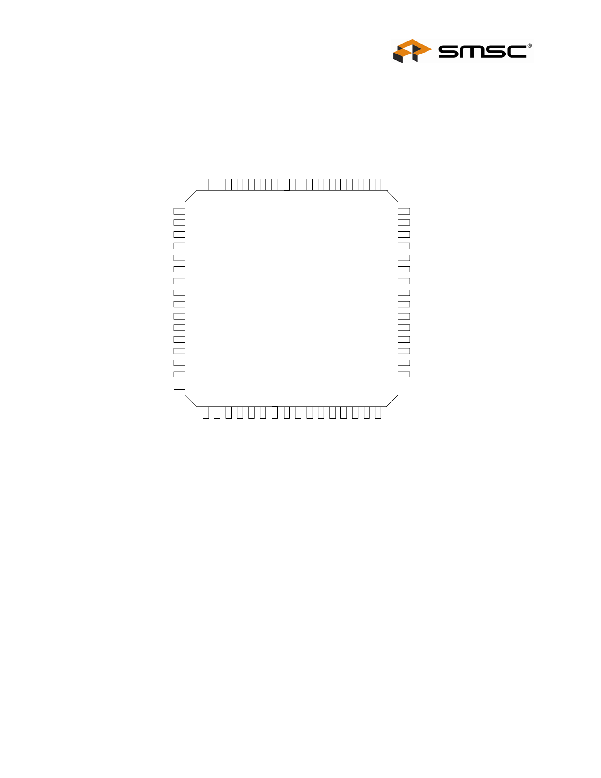
TMC2005-JT 64 PIN TQFP PACKAGE OUTLINE.............................................................................................31
SMSC TMC2005-JT Page 3 Revision 1.1 (07-24-07)
DATASHEET
Page 4
ARCNET 5 Port HUB Controller
Datasheet
MB
PIN CONFIGURATION
VSS8
RXINB0
SB
TXENB0
LB
RXINB1
NC
RXINA0
SA
TXENA0
LA
MA
RXINA1
TXENA1
VDD6
TXENB1
HM
SE
NC
LE
EXTRX
ME
VSS1
EXTTX
VDD1
CKO
VSS2
CKM2
CKM1
CKM0
NC
64 63 62 495051525354555657585960
1
2
3
4
5
6
7
8
9
10
11
12
13
14
15
16
17 18 19 20 21
RXFLT
nPLLTST
61
TMC2005-JT
22 23 24 25 26 27 28 29 30
LP
R0
VDD3
AVDD
XTLO
VSS4
NC
VDD4
XTLI
VDD2
AGS
AVSS
31
VSS3
32
48
47
46
45
44
43
42
41
40
39
38
37
36
35
34
33
VSS5
VSS7
nPULSE1
nPULSE2
nP1BAK
VDD5
nCKOEN
nRST
VSS6
nBJA
nBJB
nBJE
nMBA
nMBB
nMBE
nEXTOD
NC
Revision 1.1 (07-24-07) Page 4 SMSC TMC2005-JT
DATASHEET
Page 5
ARCNET 5 Port HUB Controller
Datasheet
BLOCK DIAGRAM
RXINA 0
RXINA 1
RXINB 0
RXINB 1
EXTRX
HM
RXFL T
SE SB SA
NOT
Circuit
NOT
Circuit
NOT
Circuit
nBJ B
nBJ E
nBJ A
Direction Control
Circuit
nMBE
nMBAMEMB
nMBB
MA L ELBLA nEXTOD
OR
Circuit
OR
Circuit
OR
Circuit
Rx
Buffer
NOT
Circuit
NOT
Circuit
NOT
Circuit
Output
Control
Circuit
Tx
Pulse
Gen.
TXENA0
TXENA1
TXENB0
TXENB1
EXTTX
nP1BAK
nPULSE1
nPULSE2
DPLL
Clock Multiplier
CKM0
CKM1
PLL
CKM2
nPLLTST
AVSS
AND
Circuit
nCKOENRO
LP
XTLO
XTLI
AVDD
AVSS
nRST
SMSC TMC2005-JT Page 5 Revision 1.1 (07-24-07)
VSS1- 8
VDD1- 6
CKO
DATASHEET
Page 6

ARCNET 5 Port HUB Controller
Datasheet
DESCRIPTION OF PIN FUNCTIONS
PIN NO. NAME INPUT/OUTPUT DESCRIPTION NOTE
1 TXENB1 OUTPUT Port B-1 Tx output to media transceiver
Setting for traffic release time (It should
2 HM INPUT
3 SE INPUT
4 NC Reserved. It should be open.
5 LE INPUT
6 EXTRX INPUT
7 ME INPUT
8 VSS1 Ground
9 EXTTX OUTPUT Port EXT. Output to media transceiver.
10 VDD1 Power Supply
11 CKO OUTPUT Clock Output
12 VSS2 Ground
13 CKM2 INPUT Network speed (data rate) setting. Pull-up
14 CKM1 INPUT Pull-up
15 CKM0 INPUT Pull-up
16 NC Reserved. It should be open.
17 RXFLT INPUT Test Pin. It should be open. Pull-up
18 nPLLTST INPUT
19 VDD2 Power Supply
20 XTLI INPUT X'tal input/External clock input.
21 XTLO OUTPUT X'tal output
22 VSS4 Ground
23 NC Reserved. It should be open.
24 VDD4 Power Supply
25 VDD3 Power Supply
26 AVDD Analog Power Supply
27 RO OUTPUT VCO output for internal PLL.
28 LP OUTPUT
29 AGS INPUT Analog sense pin for internal PLL.
30 AVSS Analog Ground
31 VSS3 Ground
32 VSS5 Ground
33 NC Reserved. It should be open.
34 nEXTOD INPUT
35 nMBE INPUT Port EXT. Noise cut (0:on, 1:off) Pull-up
36 nMBB INPUT Port A0/A1 Noise cut (0:on, 1:off) Pull-up
37 nMBA INPUT Port B0/B1 Noise cut (0:on, 1:off) Pull-up
38 nBJE INPUT
39 nBJB INPUT
40 nBJA INPUT
41 VSS6 Ground
42 nRST INPUT Internal reset signal (active Low) Pull-up
43 nCKOEN INPUT Enable of CKO output. Pull-up
be open for normal operation.) Pull-up
Port EXT. Polar assignment for EXTRX
input (0:active Hi, 1:active Low) Pull-up
Port EXT. Polar assignment of EXTTX
output (0:active Low, 1:active Hi) Pull-up
Port EXT. RX-Data input from media
transceiver. Pull-up
Port EXT. Output mode assignment of
EXTTX (0:pulse output, 1:Tx control
output) Pull-up
Test Pin for PLL.. It should connected to
VDD (Set to high)
Connection pin to loop filter for internal
PLL.
Port EXT. Open-drain mode (0:opendrain output, 1:normal output) Pull-up
Port EXT. Jitters correct mode (0:big
jitters mode, 1:normal mode) Pull-up
Port A0/A1 Jitters correct mode (0:big
jitter mode, 1:normal mode) Pull-up
Port B0/B1 Jitter correct mode (0:big
jitter mode, 1:normal mode) Pull-up
Revision 1.1 (07-24-07) Page 6 SMSC TMC2005-JT
DATASHEET
Page 7

ARCNET 5 Port HUB Controller
Datasheet
PIN NO. NAME INPUT/OUTPUT DESCRIPTION NOTE
44 VDD5 Power Supply.
45 nP1BAK OUTPUT nPULSE1 output (for backplane mode).
46 nPULSE2 OUTPUT nPULSE2 output (for normal mode).
47 nPULSE1 OUTPUT nPULSE1 output (for normal mode)
48 VSS7 Ground
49 RXINA0 INPUT
50 SA INPUT
51 TXENA0 OUTPUT Port A-0 Tx output to media transceiver.
52 LA INPUT
53 RXINA1 INPUT
54 MA INPUT
55 TXENA1 OUTPUT Port A-1 Tx output to media transceiver.
56 VDD6 Power Supply
57 NC Reserved. It should be open.
58 VSS8 Ground
59 RXINB0 INPUT
60 SB INPUT
61 TXENB0 OUTPUT Port B-0 Tx output to media transceiver.
62 LB INPUT
63 RXINB1 INPUT
64 MB INPUT
Port A-0 Rx-data input from media
transceiver. Pull-up
Port A. Polar assignment for RXINA0/A1
output (0:active Hi, 1:active Low) Pull-up
Port A. Polar assignment for TXENA0/A1
output (0:active Low, 1:active Hi) Pull-up
Port A-1 Rx-data input from media
transceiver. Pull-up
Port A. Mode assignment for
TXENA0/A1 (0:pulse output, 1:Tx control
output) Pull-up
Port B-0 Rx-data input from media
transceiver. Pull-up
Port B. Polar assignment for RXINA0/A1
input (0:active Hi, 1:Active Low) Pull-up
Port B. Polar assignment for TXENA0/A1
output (0:active Low, 1:active Hi) Pull-up
Port B-1 Rx-data input from media
transceiver. Pull-up
Port B. Mode assignment for
TXENA0/A1 (0:pulse output, 1:TX control
output) Pull-up
Note: Pull-up: Input with a pull-up resistor 70KΩ ± 30%
TX/RX Interface
FEATURE NAME INPUT/OUTPUT DESCRIPTION
RX Port RXINA [0:1]
RXINB [0:1]
EXTRX
RX Port Polar
Assignment
TX Port TX Control TXENA [0:1]
TX Port TX Data
Output
TX Port nP1BAK OUTPUT TX pulse data into RS485 driver
SMSC TMC2005-JT Page 7 Revision 1.1 (07-24-07)
SA, SB, SE INPUT Setup the polarity of RXINA [0:1],
TXENB [0:1]
EXTTX
nPULSE [1:2] OUTPUT TX pulse data into HYC9068S-
INPUT Setup the polarity by SA, SB, SE.
RXINB [0:1], EXTTX.
0 : active H
1: active L
OUTPUT TX data pulse (Mx=0) or TX
enable signal (Mx=1).
Setup TX mode by MA, MB, ME.
Setup the polarity by LA, LB, LE
SK/9088S-SK when ARCNET
chip is at normal mode.
The pulse is always active Low.
or HYC2485S/2488S when
ARCNET chip is at backplane
DATASHEET
Page 8

ARCNET 5 Port HUB Controller
Datasheet
FEATURE NAME INPUT/OUTPUT DESCRIPTION
mode.
The pulse is always active Low.
TX Port Polarity
Setup
TX Port Mode Setup MA, MB, ME INPUT Setup the mode of TXENA [0:1],
Operating Mode Setup
FEATURE NAME
Data rate
CKM [0:2] INPUT
setup
Noise cut
mode
nMBA
nMBB
nMBE
Big jitter
mode
nBJA
nBJB
nBJE
Open drain
nEXTOD INPUT Setup a the use of EXTTX port.
mode
PLL
FEATURE NAME
LP OUTPUT
RO OUTPUT VCO output
AGS INPUT Analog sense input.
Revision 1.1 (07-24-07) Page 8 SMSC TMC2005-JT
LA, LB, LE INPUT Setup the polarity of TXENA
[0:1], TXENB [0:1], EXTTX.
0 : active L
1: active H
TXENB [0:1], EXTTX.
0: Output TX pulse. (It is
equivalent to nTXEN “OR”
nP1BAK)
1: Output TX enable
INPUT/
OUTPUT
DESCRIPTION
Terminal to setup the data rate of TMC2005.
CKM2 CKM1 CKM0 DIVISOR MULTIPLIER SPEED
0 0 0 16 x1 156.25 Kbps
0 0 1 8 x1 312.5 Kbps
0 1 0 4 x1 625 Kbps
0 1 1 2 x1 1.25 Mbps
1 0 0 1 x1 2.5 Mbps
1 0 1 1 x2 5 Mbps
1 1 0 Reserved Reserved Reserved
1 1 1 1 x4 10 Mbps
External clock is 20MHz.
Refer to “VARIOUS SETUP”
INPUT 0: Cut off noise from received data
1: Don’t cut off noise
Setup “0” normally.
INPUT Setup a jitter filter feature.
Select a pulse as reference phase used by DPLL.
nd
0: 2
pulse (big jitter mode)
st
1: 1
pulse (normal mode)
INPUT/
OUTPUT
0: Set EXTTX as open drain output and use as Ext.
1: Set EXTTX as normal output and use as 5
DESCRIPTION
th
port.
Using PLL: Connect to an external condenser
“C1” for loop filter.
Using no PLL: must be open.
Using PLL: Connect to an external resistor “R0” for
loop filter.
Using no PLL: must be open.
Using PLL: Connect to loop filter.
Using no PLL: Connect to ground.
DATASHEET
Page 9
ARCNET 5 Port HUB Controller
Datasheet
FEATURE NAME
nPLLTST INPUT Test pin for PLL.
AVDD Analog power supply
AVSS Analog ground
INPUT/
OUTPUT
DESCRIPTION
Must always connect to VDD.
Using PLL: Analog power supply. There are some
limits on PCB pattern.
Using no PLL: Power supply (+5V) same as VDD1~6.
Using PLL: Analog ground. There are some limits on
PCB pattern.
Using no PLL: Use a ground same as VSS1~8.
Other Signals
FEATURES
CRYSTAL
INTERFACE
CRYSTAL
INTERFACE
SYSTEM RESET
INTERFACE
TEST PIN CKO OUTPUT Output internal clock of TMC2005.
TEST PIN nCKOEN INPUT Output control of CKO.
TEST PIN RXFLT INPUT It must be open
TEST PIN NC [1:2] It must be open
POWER SUPPLY VDD [1:6] Power supply (+5V)
GROUND VSS [1:8] Ground
NAME
XTLI INPUT Connect a 20MHz crystal.
XTLO OUTPUT Connect a 20MHz crystal.
nRST INPUT Reset for initializing TMC2005. (active
INPUT/
OUTPUT
DESCRIPTION
When supplying an external clock,
input the clock to this pin.
When supplying an external clock, it
must be open.
Low)
0: Output internal clock on CKO.
1: Always output Low level on CKO.
Set “1” Normally.
SMSC TMC2005-JT Page 9 Revision 1.1 (07-24-07)
DATASHEET
Page 10

ARCNET 5 Port HUB Controller
Datasheet
OPERATIONAL DESCRIPTION
Direction Determination
All TX ports are set to disable mode in the initial state. When a signal is received from any RX ports, the circuit holds
the port on receiving mode (disable TX) and changes the other ports to sending mode (disable RX). One port stays in
RX and the rest change into TX after all. The circuit initializes the internal DPLL on the timing of received RX pulse,
and the RX buffer circuit stores the RX data and filters its jitter. TX controlling circuit regenerates the stored RX pulse
on nPULSE1, nPULSE2 and nP1BAK. The nPULSE1 and nPULSE2 are pulse output pins for transceivers
(HYC9088A) of ARCNET normal mode. The nP1BAK is a pulse output pin for transceiver (HYC5000/4000/2000 and
RS485 driver) of ARCNET back plane mode. When using optical transceiver, instead of these signals, TXENA [0:1],
TXENB [0:1], EXTTX (MA, MB, ME = 0) must be used as TX data inputs of the optical transceiver.
Direction Release
On ARCNET protocol, each TX message starts with 6-bits of “1” ALERT and each data byte is lead by three bits (1, 1,
0) preamble. To control the HUBs direction, the circuit monitors this bit pattern and holds the state. If the end of the bit
pattern comes, all TX ports return receiving mode (disable TX) again. The interval timer detects the end of the bit
pattern. During data is on line, silent period is less than 4 uS* because at least one bit “1” among 10-bits is received
while receiving the data. The minimum silent interval from the end of received data to the alert of the next data (the
minimum time of changing the direction) is the chip turn around time (12.6 uS*) of ARCNET controller. The interval
timer to detect the data end is set to 5.6uS by adding some margin to the above interval for neglecting the reflection
on a cable.
[Note] Numbers marked * are at 2.5Mbps operation.
Jitter Filter
To build a network with transceivers that introduce big jitter like ones for optical fiber, the old HUB that has direction
control only may cause a transmission error because jitters on each HUB are added when several HUBs were
connected in serial. The TMC2005 fixes that problem with jitter filtering and wave shaping through the following three
steps.
1) Input Sampling
The TMC2005 samples a data on a network by eight times clock of the network data.
2) Jitter Filtering (DPLL)
The TMC2005 filters the jitter (± 100nS at 2.5Mbps) of network data sampled by 8X clock through the internal digital
PLL and stores the data into the buffer.
3) Wave Shaping Output
The TMC2005 re-synchronizes and regenerates the network data at the same clock as the data rate.
The capability of the jitter filtering is shown below.
DATA RATE CAPABILITY OF JITTER FILTERING
10Mbps ± 25nS
5Mbps ± 50nS
2.5Mbps ± 100nS
1.25Mbps ± 200nS
625Kbps ± 400nS
312.5Kbps ± 800nS
156.25Kbps ± 1.6uS
Revision 1.1 (07-24-07) Page 10 SMSC TMC2005-JT
DATASHEET
Page 11
ARCNET 5 Port HUB Controller
Datasheet
Option Feature for Jitter Filtering
When any RX ports receive the bigger jitter than its allowance, the TMC2005 may fail to receive the data
correctly and the network may be down.. However the below method to escape is effective for the case that a
momentary big jitter occurs under a special condition like an optical transceiver.
1) Big jitter (BJ) mode
The reference phase of the internal DPLL is changed from the first pulse to the second pulse by setting “0” to the big
jitter mode pins (nBJX). This setup is effective for the case that a big jitter occurs when rising up from DC state as
same as when using an optical transceiver with ATC function (refer to complement).
Note: The delay time of the TMC2005 becomes 400nS (at 2.5Mbps) longer than the normal mode. The delay time
limits the maximum cable length and maximum node number.
[Complement] The big jitter may occur in the case of using an optical transceiver, especially an optical receiver that
has an ATC circuit that controls threshold level in proportion to received light strength. The first pulse especially after
long time idle has the big jitter but the second pulse is stabilized.
2) Changing polar of RX port
In order to filter the jitter of edge in one side, it is effective to set reverse to pin SA, SB, SE to change the polarity of
RX port.
Note: Changing the polarity of RX port makes the delay time of the TMC2005 circuit a half bit (200nS) longer than
original 2.5Mbps, and the delay time affects the maximum cable length and maximum node number.
Option Feature for Noise Cut mode
The Noise cut mode is enabled by setting pin nMBx sets 0. The noise cut mode is a function to remove the ringing
noise and the reflection noise generated on the leading edge side of the input pulse to receive data input RXINx. The
position and the width of the “dead band” are shown in the figure below.
- Dead band at Normal mode (nMBx=1) - Dead band at Noise cut mode (nMBx=0)
Period of data rate (Tdr)
Tdr/8 = 1 clock Tdr/8 = 1 clock
RXIN RXIN
(Active High)
Ideal waveform
dead band
RXIN edge reference position:
Generated by adjacent phase of SYNC character (1,1,0)
(Active High)
Ideal waveform
RXIN edge reference position:
Generated by adjacent phase of SYNC character (1,1,0)
Period of data rate (Tdr)
dead band: Noise cut band
SMSC TMC2005-JT Page 11 Revision 1.1 (07-24-07)
DATASHEET
Page 12
ARCNET 5 Port HUB Controller
Datasheet
APPLICATION NOTES
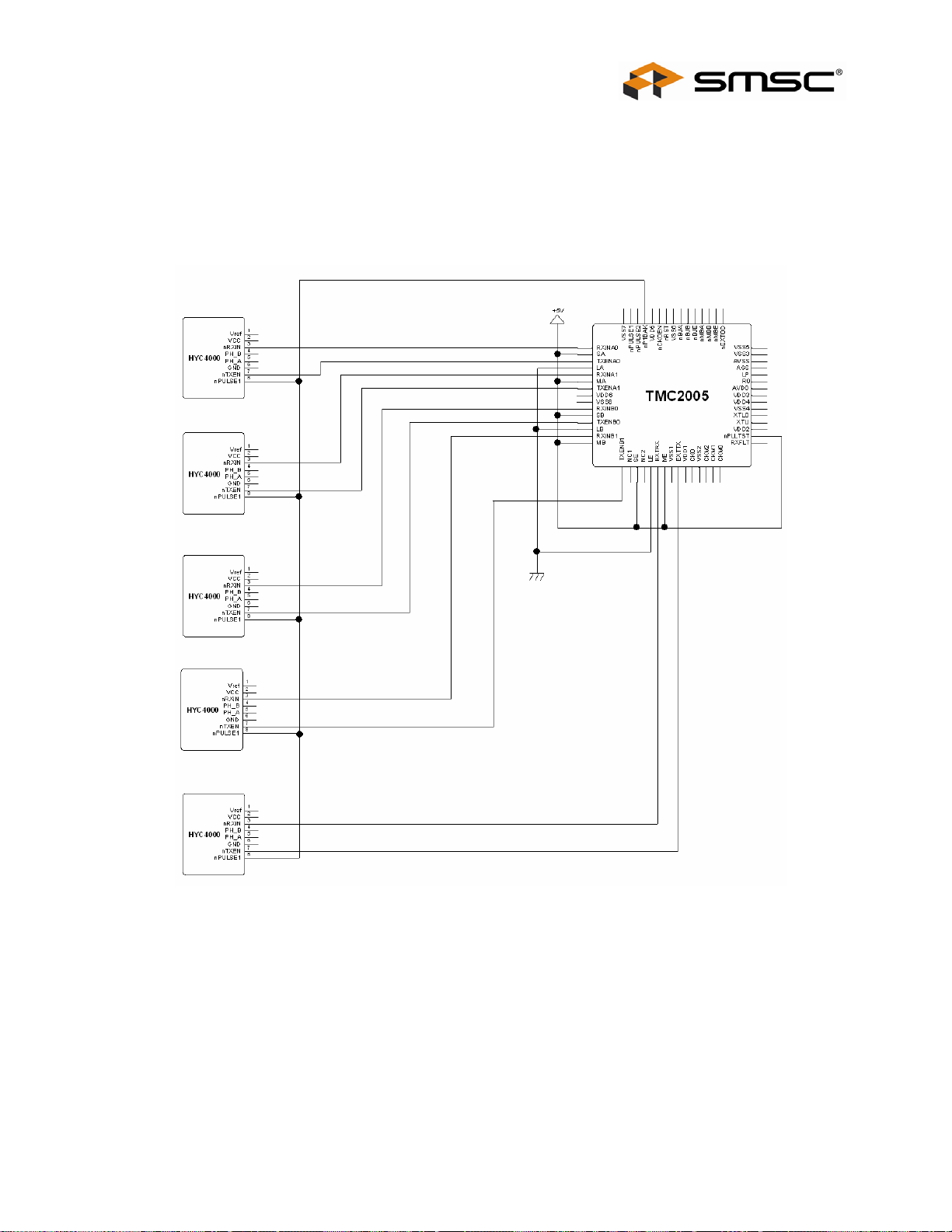
Example 1: A five ports HUB with HYC4000s in backplane mode.
FIGURE 1 - APPLICATION EXAMPLE
Only the TMC2005 and five transceivers are indicated in the above figure. Connect the other pins adequately.
Revision 1.1 (07-24-07) Page 12 SMSC TMC2005-JT
DATASHEET
Page 13
ARCNET 5 Port HUB Controller
Datasheet
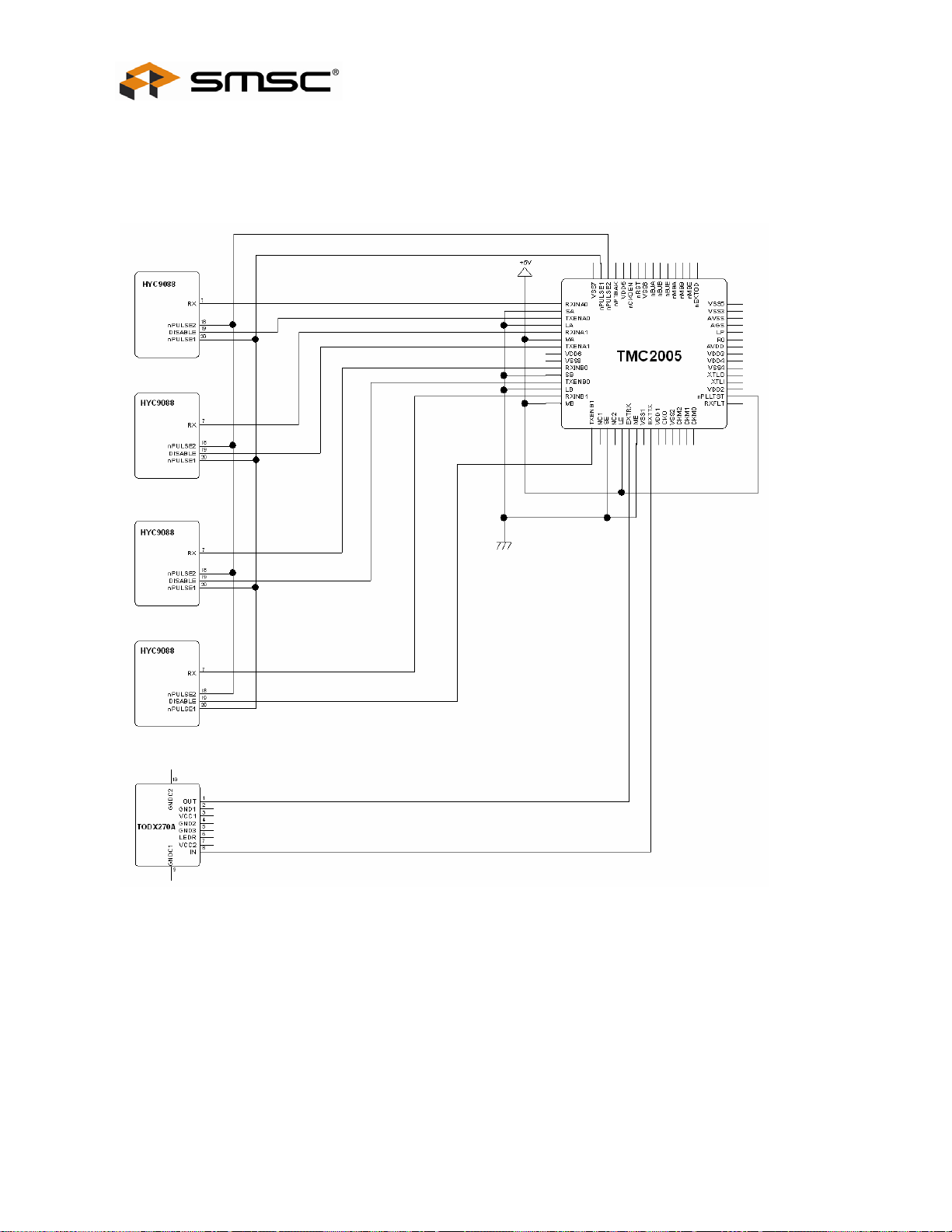
Example 2: A five ports HUB with HYC9088s and a optical transceiver(TODX270A) links the two physical layers;
dipulse and fiber optics.
FIGURE 2 - APPLICATION EXAMPLE 2
Only the TMC2005 and five transceivers are indicated in the above figure. Connect the other pins adequately.
SMSC TMC2005-JT Page 13 Revision 1.1 (07-24-07)
DATASHEET
Page 14

ARCNET 5 Port HUB Controller
Datasheet
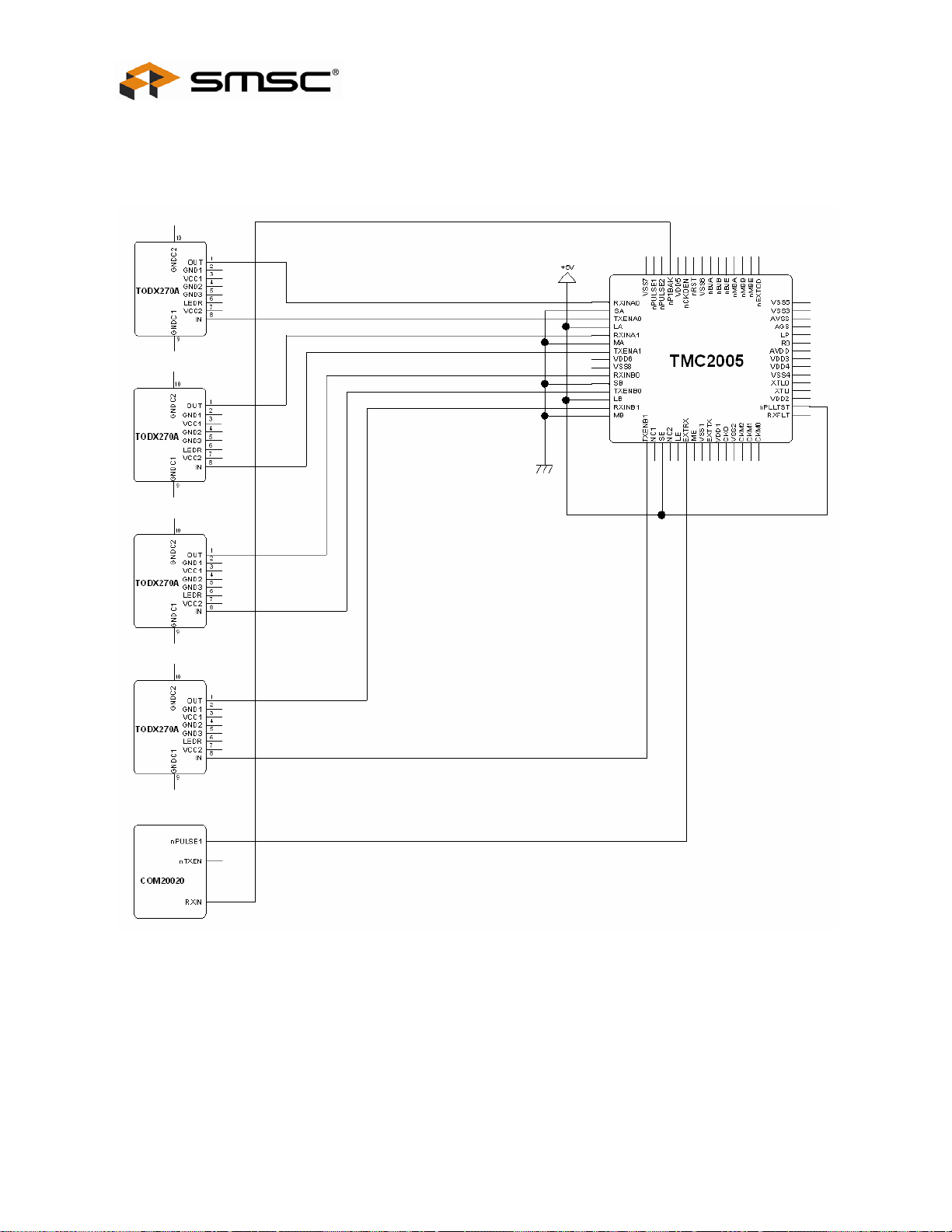
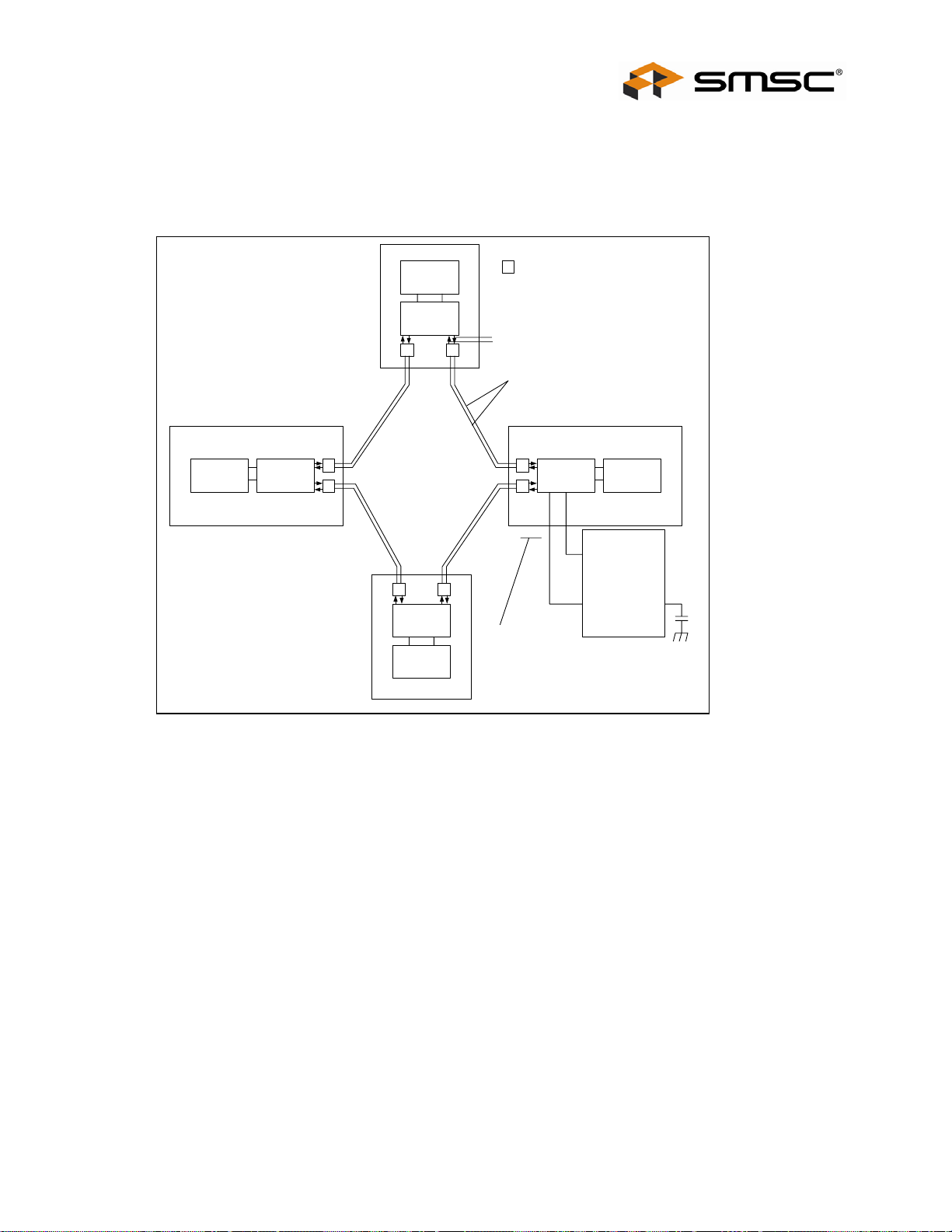
Example 3: A five ports HUB with two optical transceivers, two HYC9088s, and a HYC4000 links three physical
layers; fiber optics, dipulse, and AC-485.
FIGURE 3 - APPLICATION EXAMPLE 3
Only the TMC2005 and five transceivers are indicated in the figure above. Connect the other pins properly.
Revision 1.1 (07-24-07) Page 14 SMSC TMC2005-JT
DATASHEET
Page 15
ARCNET 5 Port HUB Controller
Datasheet
Example 4: An on-board type HUB with a COM20020 and four optical transceivers in backplane mode.
FIGURE 4 - APPLICATION EXAMPLE 4
Only the TMC2005 and four transceivers with the COM20020 are indicated in the above figure. Connect the other
pins adequately.
SMSC TMC2005-JT Page 15 Revision 1.1 (07-24-07)
DATASHEET
Page 16

ARCNET 5 Port HUB Controller
Datasheet
Example 5: An on-board type HUB with a COM20020 and four RS485 transceivers.
FIGURE 5 - APPLICATION EXAMPLE 5
Only the TMC2005 and four transceivers with the COM20020 are indicated in the above figure. Connect the other
pins adequately.
Revision 1.1 (07-24-07) Page 16 SMSC TMC2005-JT
DATASHEET
Page 17

ARCNET 5 Port HUB Controller
Datasheet
Example 6: An on-board type HUB with a COM20020, two HYC4000s, and two HYC9088s links two different physical
layers; dipulse and AC-485.
FIGURE 6 - APPLICATION EXAMPLE 6
Only the TMC2005 and four transceivers with the COM20020 are indicated in the above figure. Connect the other
pins adequately.
SMSC TMC2005-JT Page 17 Revision 1.1 (07-24-07)
DATASHEET
Page 18
ARCNET 5 Port HUB Controller
Datasheet
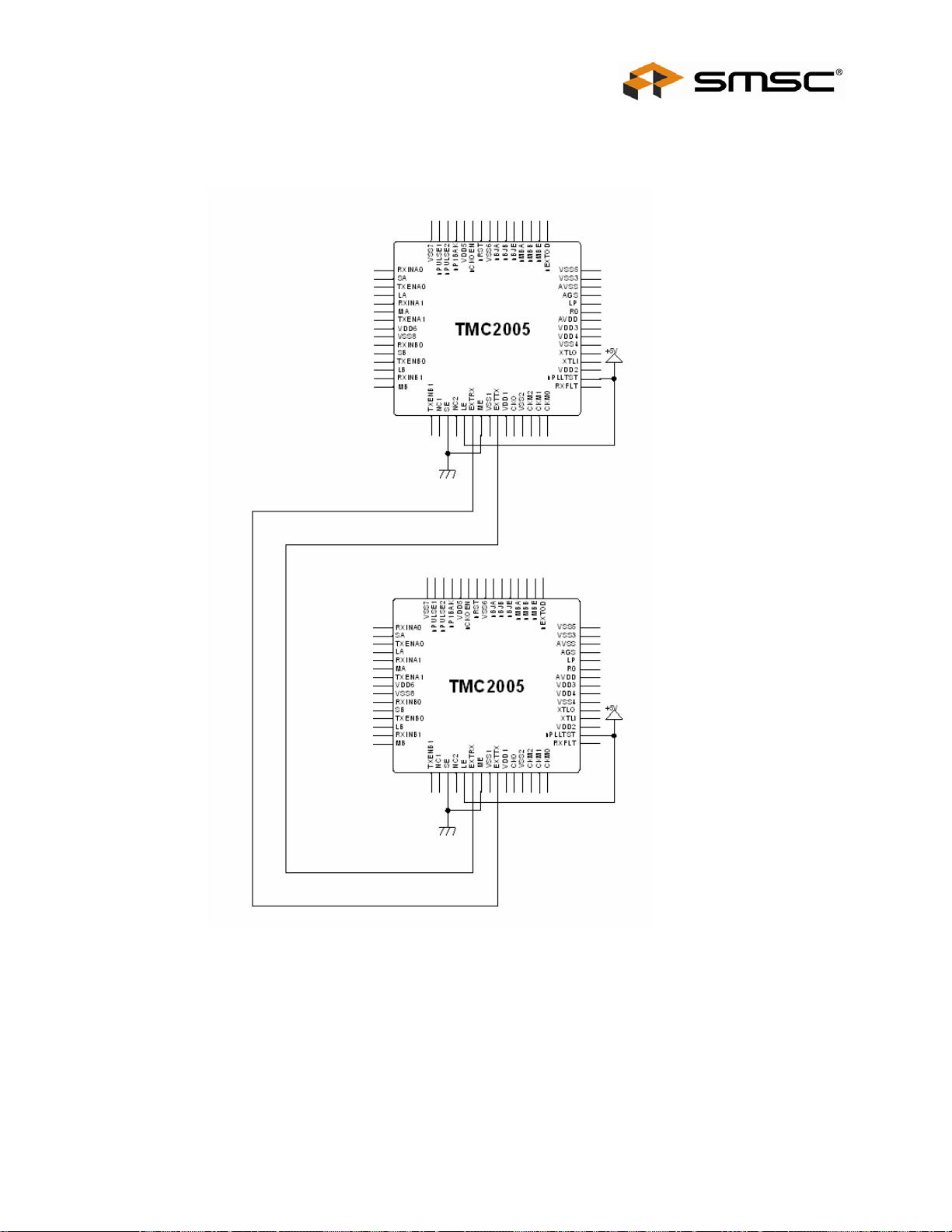
Example 7: An eight ports HUB are composed by using two TMC2005. Two TMC2005 connects the EXTTX signal
with the EXTRX signal.
FIGURE 7 - APPLICATION EXAMPLE 7
Only the two TMC2005s are indicated in the above figure. Connect the other pins adequately.
Revision 1.1 (07-24-07) Page 18 SMSC TMC2005-JT
DATASHEET
Page 19

ARCNET 5 Port HUB Controller
Datasheet
Example 8: A sixteen ports HUB are composed by using four TMC2005. The EXT port between TMC2005 is made an
open-drain mode and it connects it (left example). Or put standard logic IC such as 74LS20 outside (right example).
This connected method is excellent in noised respect compared with connected method of open-drain mode.
Data rate: 5Mbps and below Data rate: 10Mbps and below
or
FIGURE 8 - APPLICATION EXAMPLE 8
Only the four TMC2005s are indicated in the above figure. Connect the other pins adequately.
Note: Use the wiring pattern length that connects between four TMC2005s by five inches or less in open-drain mode.
Four TMC2005s is maximum in open-drain mode.
SMSC TMC2005-JT Page 19 Revision 1.1 (07-24-07)
DATASHEET
Page 20

ARCNET 5 Port HUB Controller
Datasheet
PORT GROUP
The five ports can be divided into three groups (group A: two ports, group B: two ports, extension port: one port) and
each group can select TX/RX polar, noise cut mode, and big jitter mode respectively. Select pins for each group are
as follows:
FUNCTION GROUP A GROUP B EXTENSION
RECEIVE RXINA0, 1 RXINB0, 1 EXTRX
TRANSMIT TXENA0, 1 TXENB0, 1 EXTTX
RX POLARITY SA SB SE
TX POLARITY LA LB LE
TX CONTROL MA MB ME
NOISE CUT nMBA nMBB nMBE
BIG JITTER nBJA nBJB nBJE
EXTENSION nEXTOD
Various Setup
Example For Operation Mode Setup To Each Port
SA, SB, SE LA, LB, LE MA, MB, ME RX POLAR TX POLAR TRANSCEIVER
1 0 1 Active Low Active Low HYC2485S/HYC2488S
0 1 0 Active High Active High Optical Transceiver
0 0 1 Active High Active Low HYC9088/HYC9068
1 1 1 Active Low Active High RS485 Transceiver
Note for Unused port
Unused ports can be left open because RX port (RX input), RX polar (S input), TX polar (L input), TX control (M input)
pins have internal pull-up resistors. Because of internal pull-up resistors, select pins for noise cut (nMB input), big
jitter (nBJ input) can be left open when used for setting “OFF”.
Example for Power-On Reset Circuit
FIGURE 9 - POWER-ON RESET
Revision 1.1 (07-24-07) Page 20 SMSC TMC2005-JT
DATASHEET
Page 21

ARCNET 5 Port HUB Controller
Datasheet
CONNECTING THE TMC2005 WITH INTERNAL PLL
When using the TMC2005 at data rate 2.5Mbps or lower, it is not necessary to use internal PLL. Leave the loop filter
pins (RO, LP) open and connect AGS to the Ground. The pins for the analog power supply (AVSS, AVDD) may
connect to digital power supply. When using the TMC2005 at data rate 5Mbps or higher, the internal PLL has to be
used as a clock multiplier. PCB layout must follow the guidelines at Figure 10, refer to Notes 1 through 5.
FIGURE 10 - PLL PATTERN LAYOUT
Note 1: Prohibit the patterns for LP and RO from occupying the area of digital power supply. Use the area of analog
power supply between VAA and AVSS.
Note 2: Encircle the pattern between LP, RO and AGS with wide pattern of analog ground.
Note 3: Connect the analog power supply “VAA” with 0.1 uF condenser (a) with in 1/8 inch (~ 3.2mm) from VAA pin.
Note 4: In order to filter the jitter of low frequency, connect a 10 uF condenser (b) in parallel with the condenser (a).
Note 5: Place 0.1 uF bypass condenser (c) within ¼ inch (~ 6.4mm) from VDD3 and VSS3. Connect the ground side
of a condenser (c) at the place (*) where AVSS returns to GND plane.
SMSC TMC2005-JT Page 21 Revision 1.1 (07-24-07)
DATASHEET
Page 22

ARCNET 5 Port HUB Controller
Datasheet
Method To Connect A Crystal Clock
Connect with external parts as follows:
FIGURE 11 - CONNECTING THE CRYSTAL CLOCK
Note 1: When designing a printed circuit board, keep the patterns as short as possible and don’t cross with other
patterns.
Note 2: When using an external clock like an oscillator module, connect it to XTLI pin and leave XTLO pin open.
When designing a printed circuit board, wire between XTLI pin and oscillator should be short as possible.
nPLLTST pin
nPLLTST must be connect toVDD. The rest of input pins have pull-up resistors built in, but nPLLTST pin does not
have the pull-up resistor. Clock signal cannot ditributed into the TMC2005 if nPLLTST pin is connected GND or is left
open.
Revision 1.1 (07-24-07) Page 22 SMSC TMC2005-JT
DATASHEET
Page 23

ARCNET 5 Port HUB Controller
Datasheet
CASCADING CONNECTION
HUBs can be connected in cascade by using the ports as Fig. 12. In the case of cascade connection, it is necessary
to consider how many HUBs can exist in serial. The maximum delay between input port and output port is 650ns
@2.5Mbps at the TMC2005. It is equivalent to the propagation delay when a cable length is 135m. For example, if
every cable length is 10m in Figure 12, the longest distance is physically 50m but it is electrically 590m because of
multiplying 10m by 5 and 135m by 4, and the total propagation delay becomes 2.8uS. For analyzing the network
timing, consider the delay caused by HUBs. In the ARCNET protocol, it is defined that the longest distance between
nodes is the maximum 6.4Km. For example, if 20 TMC2005s exist between nodes in the longest distance, the actual
cable length is 3.7Km because of deducting 135m by 20 in converting to cable length from 6.4Km.
TMC2005
TMC2005
TMC2005
TMC2005
Port 2
Port 1
Port 4
Port 3
Port 5
54321
Port 2
Port 1
Port 4
Port 3
Port 5
54321
Port 2
Port 1
Port 4
Port 3
Port 5
54321
Port 2
Port 1
Port 4
Port 3
Port 5
54321
NODE NODE
FIGURE 12 - CASCADE CONNECTION OF 4 HUBS
Two examples of eight ports HUBs using two TMC2005s are shown in Fig. 13 and 14. If connecting as in Fig. 13,
eight TMC2005s exist between the nodes at both far ends. On the other hand, when assigning two ports for
cascading connection to the same TMC2005, the number of TMC2005 in serial connection can be down to the
number of HUBs plus two, which can reduce the propagation delay.
SMSC TMC2005-JT Page 23 Revision 1.1 (07-24-07)
DATASHEET
Page 24

ARCNET 5 Port HUB Controller
Datasheet
HUB 1 HUB2 HUB 3 HUB4
TMC2005 TMC2005
432
1
432
1
NODE NODE
HUB 1 HUB2 HUB 3 HUB4
TMC2005 TMC2005
432
1
432
1
NODE NODE
TMC2005 TMC2005
TMC2005 TMC2005
234
234
5
5
432
1
1
234
432
234
5
5
432
1
1
234
432
234
FIGURE 13 - CASCADE CONNECTION OF 8 PORT HUB
234
234
TMC2005 TMC2005
5
5
432
1
1
234
5
432
234
5
TMC2005 TMC2005
432
1
1
234
432
234
FIGURE 14 - CASCADE CONNECTION OF 8 PORT HUB
TMC2005 TMC2005
5
5
5
5
432
1
432
1
TMC2005 TMC2005
1
1
234
432
432
234
234
234
5
5
5
5
Revision 1.1 (07-24-07) Page 24 SMSC TMC2005-JT
DATASHEET
Page 25

ARCNET 5 Port HUB Controller
Datasheet
Fig.15 shows a 16 ports HUB with four TMC2005s connected by open–drain ports. When assigning two ports for
cascade connection to the same TMC2005, the number of TMC2005s for serial connection can be reduced to the
number of HUBs plus two.
HUB2 HUB 3
TMC2005 TMC2005
432
1
1
1
432
1
HUB 1 HUB 4
234
234
TMC2005 TMC2005
432
1
1
234
1
432
234
1
TMC2005 TMC2005
432
1
1
234
1
432
234
1
TMC2005 TMC2005
432
1
1
234
1
432
234
1
TMC2005 TMC2005
432
1
432
1
1
1
234
234
TMC2005 TMC2005
432
1
1
234
1
432
234
1
TMC2005 TMC2005
432
1
432
1
1
1
234
234
TMC2005 TMC2005
432
1
1
234
1
432
234
1
NODE NODE
FIGURE 15 - CASCADE CONNECTION OF 16 PORT HUB
Note: When connecting TMC2005 by open-drain output on a board, connecting TMC2005s must be four or less,
and the data rate must be 5Mbps or slower. The pattern of open-drain output has to be as short as possible
(less than 15cm).
SMSC TMC2005-JT Page 25 Revision 1.1 (07-24-07)
DATASHEET
Page 26
ARCNET 5 Port HUB Controller
Datasheet
Ring Network With the TMC2005
The reliability of the network can be improved by connecting every node in a ring, because the communication is
maintained through the reverse route even if the cable is cut at a point. However ARCNET controller alone can not
support ring, because ARCNET is a half-duplex communication system. Using HUBs makes possible for ARCNET to
built a ring network as in Fig.16. This configuration is available only for using fiber optics. (Refer to the application note
for details.)
COM20020
TMC2005
TMC2005COM20020
TMC2005
COM20020
FIGURE 16 - RING CONFIGURATION
Note 1: Noise may cause an endless loop in a ring system, and the network may hang up. Therefore take care of
designing the patterns between TMC2005 and transceiver or cabling of system.
Example for system hang-up
- A noise occurs only at “A” point in Figure 16.
- The noise propagates clockwise on the network.
- TMC2005 detects the noise that came back through the ring.
- The noise causes an endless loop in the ring.
Example for no hang-up
- Any noise occurs at “A” and “B” points in Figure 16 at the same time.
- The noise propagates to both directions in the network.
- An endless loop doesn’t occur because TMC2005s in the middle absorb the noise from both sides.
Note 2: Place a watch dog timer on one of the TMC2005 in at least one ring. To protect from hang-up the detecting
time of the watch dog timer should be set to longer than 2.7 mS (@ 2.5Mbps) that is the burst time in the
ARCNET protocol.
Note 3: Consider that a total of each segment delay time (cable delay, TMC2005 delay, driver delay and receiver
delay) between HUBs in a network is less than 5.6uS (@ 2.5Mbps). The maxmimum distance between
HUBs is approximiately 1000m (@ 2.5Mbps).
Revision 1.1 (07-24-07) Page 26 SMSC TMC2005-JT
Optical Transceiver
A
B
Optical Fiber
TXEN
TXEN of any port
TMC2005 COM20020
nRST
nRESET
CK
CT
DATASHEET
Page 27
ARCNET 5 Port HUB Controller
Datasheet
OPERATIONAL DESCRIPTION
MAXIMUM GUARANTEED RATINGS*
Stresses above those listed may cause permanent damage to the device. This is a stress rating only and functional
operation of the device at these or any other condition above those indicated in the operational sections of this
specification is not implied.
(Note) When powering this device from laboratory or system power supplies, it is important that the Absolute
Maximum Ratings not be exceeded or device failure can result. Some power supplies exhibit voltage spikes or
“glitches” on their output when the AC power is switch on or off. In addition, voltage transients on the AC power line
may appear on the DC output. If this possibility exists it is suggested that a clamp circuit be used.
Vss = 0V
ITEM SYMBOL RATING UNIT
POWER SUPPLY VOLTAGE VDD -0.3 +7.0 V
INPUT VOLTAGE VIN -0.3 VDD +0.3 V
OUTPUT VOLTAGE VOUT -0.3 VDD +0.3 V
AMBIENT TEMPERATURE Tstg -40 +125 °C
STANDARD OPERATING CONDITION
Vss = 0V
ITEM SYMBOL RATING UNIT
POWER SUPPLY VOLTAGE VDD 4.5 – 5.5 V
AMBIENT TEMPERATURE Ta 0 - +85 °C
DC CHARACTERISTIC - INPUT PIN
SYMBOL ITEM CONDITION MIN MAX UNIT
VIH
VIL
IIH
IIL
IIL
IOZ
IDD
High Level Input Voltage
Low Level Input Voltage 0.8 V
High Level Input Current VIN=VDD -10 10 uA
Low Level Input Current VIN=VSS -10 10 uA
With pull-up Vin=VSS -200 -10 uA
Output Leak Current VOUT=VDD or VSS -10 10 uA
Dissipation Current Operating 100 mA
XTLI, nPLLTST 3.5 V
Others 2.2 V
SMSC TMC2005-JT Page 27 Revision 1.1 (07-24-07)
DATASHEET
Page 28

ARCNET 5 Port HUB Controller
Datasheet
DC CHARACTERISTIC - OUTPUT PIN
SYMBOL ITEM CONDITION MIN MAX UNIT PIN
VOH High Level Output Voltage IOH=-4mA 2.4 V 1,9,46,51,
VOH High Level Output Voltage IOH=-8mA 2.4 V 11,45,47
VOL Low Level Output Voltage IOL=4mA 0.4 V 1,9,46,51,
VOL Low Level Output Voltage IOL=8mA 0.4 V 11,45,47
AC CHARACTERISTIC - CLOCK and RESET
ITEM SYMBOL MIN TYP MAX UNIT CONDITION
Generating Static Time tx 4 mS
Clock Cycle tCYC 50 nS Note 1
Clock Frequency Deflection tCDF -100 100 ppm Note 1
Clock Pulse Width tCW 20 nS Note 1
Reset Pulse Width ttRSW 200 nS Note 1
Note 1: Use only F=20MHz
Note 2: VDD=4.5V
XTLI
t
CW
nRST
t
RSW
t
CW
FIGURE 17 - CLOCK AND RESET
t
CYC
55,61
55,61
Revision 1.1 (07-24-07) Page 28 SMSC TMC2005-JT
DATASHEET
Page 29
ARCNET 5 Port HUB Controller
Datasheet
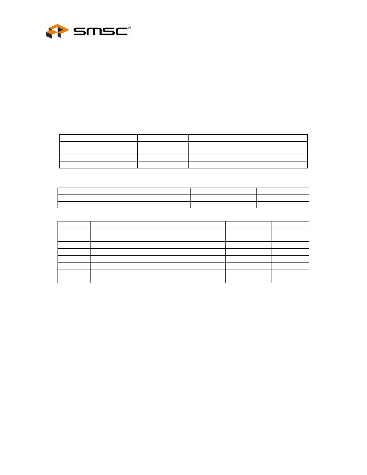
AC CHARACTERISTIC – Rx waveforms and Tx waveforms
t2
t1
RXI Nx (S=1)
(Received port)
TXENy (M=1, L=0)
* 4 ports except received port
nP1BAK
/TX ENy (M =0, L =0)
* 4 ports except received port
nPULSE1
nPULSE2
t3
t4 t5
t11
t6
t12
t16
t8
t7
t9
t13
t14
t18
t17
t19
t10
t15
FIGURE 18 - RX WAVEFORMS AND TX WAVEFORMS
ITEMS MARK MIN TYP MAX UNIT REMARK
RXIN Low Pulse Width
RXIN High Pulse Width
RXIN Period
RXIN First Active Edge to TXEN Active
RXIN Last Active Edge to TXEN Inactive
RXIN First Active Edge to
nP1BAK/TXEN First Active Edge
nP1BAK/TXEN Low Pulse Width
nP1BAK/TXEN High Pulse Width
nP1BAK/TXEN Period
t1 15 nS
t2 15 nS
Tdr
t3
nS
(Value at 2.5Mbps)
(400)
2/8Tdr 3/8Tdr+50
t4
(100)
111/8Tdr 112/8Tdr+50
t5
(5,550)
9/8Tdr 10/8Tdr+50
t6
(450)
1/2Tdr
t7
(200)
1/2Tdr
t8
(200)
Tdr
t9
(400)
(200)
(5,650)
(550)
nS
nS
nS
Note1
nS
(Value at 2.5Mbps)
Note1
nS
(Value at 2.5Mbps)
Note2, Note3
nS
(Value at 2.5Mbps)
Note2
(Value at 2.5Mbps)
Note2
(Value at 2.5Mbps)
Note2
(Value at 2.5Mbps)
RXIN Active Edge to
nP1BAK/TXEN Active Edge
(Except First Edge of RXIN)
t10
5/8Tdr 9/8Tdr+50 14/8Tdr+50
(250) (500) (750)
Note2, Note3
nS
(Value at 2.5Mbps)
SMSC TMC2005-JT Page 29 Revision 1.1 (07-24-07)
DATASHEET
Page 30

ARCNET 5 Port HUB Controller
Datasheet
ITEMS MARK MIN TYP MAX UNIT REMARK
RXIN First Active Edge
to nPULSE1 First Active Edge
nPULSE1 Low Pulse Width
nPULSE1 High Pulse Width
nPULSE1 Period
RXIN Active Edge to
nPULSE1 Active Edge
(Except First Edge of RXIN)
nPULSE1 to nPULSE2 Overlap
nPULSE2 Low Pulse Width
nPULSE2 High Pulse Width
t11
9/8Tdr 10/8Tdr+50
(450)
(550)
Note3
nS
(Value at 2.5Mbps)
1/4Tdr
t12
nS
(Value at 2.5Mbps)
(100)
3/4Tdr
t13
nS
(Value at 2.5Mbps)
(300)
Tdr
t14
nS
(Value at 2.5Mbps)
(400)
t15
5/8Tdr 9/8Tdr+50 14/8Tdr+50
(250) (500) (750)
t16 -10 0 +10 nS
Note3
nS
(Value at 2.5Mbps)
1/4Tdr
t17
nS
(Value at 2.5Mbps)
(100)
3/4Tdr
t18
nS
(Value at 2.5Mbps)
(300)
nPULSE2 Period
t19
nS
(400)
Tdr: Period of data rate, ex) Tdr=400nS at 2.5Mbps
Note1: Applied to TXENx which is set to Mx=1. (Tx Control mode)
Note2: Applied to TXENx which is set to Mx=0. (Pulse output mode)
Note3: Extra one “Tdr” time to be added at RXINx is set to nBJx=0. (Big Jitter mode)
Tdr
(Value at 2.5Mbps)
Revision 1.1 (07-24-07) Page 30 SMSC TMC2005-JT
DATASHEET
Page 31
ARCNET 5 Port HUB Controller
Datasheet
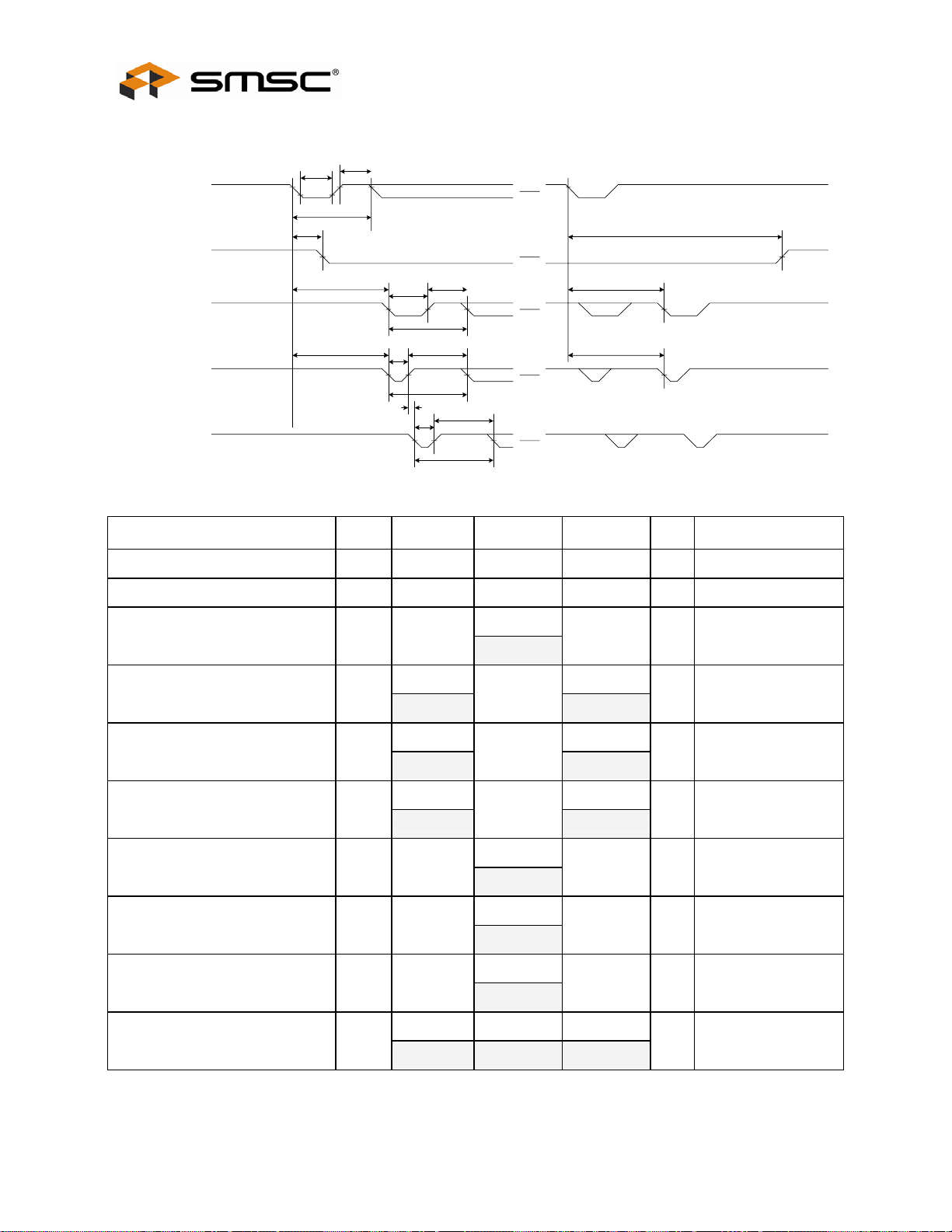
TMC2005-JT 64 PIN TQFP PACKAGE OUTLINE
D
D1
Ze
E1 E
64
1
Zd
SYMBOL MIN (mm) TYP (mm) MAX (mm)
D
D1
E
E1
Ze
Zd
11.8 12.0 12.2
9.9 10.0 10.1
11.8 12.0 12.2
9.9 10.0 10.1
1.25 typ
1.25 typ
SMSC TMC2005-JT Page 31 Revision 1.1 (07-24-07)
DATASHEET
Page 32

ARCNET 5 Port HUB Controller
A
A
Datasheet
b bbb M aaa
SYMBOL MIN (mm) TYP (mm) MAX (mm)
A 1.6
A1
A2
B
E
aaa
bbb
0.95 0.1 0.15
1.35 1.4 1.45
0.17 0.22 0.27
e
0.5 BSC
0.08
0.08
c
L
SYMBOL MIN (mm) TYP (mm) MAX (mm)
c
L
0.9 0.145 0.2
0.45 0.6 0.75
A2
1
Revision 1.1 (07-24-07) Page 32 SMSC TMC2005-JT
DATASHEET
 Loading...