

SMSC PPC34C60 Datasheet

Parallel Port Interface Chip - Peripheral Side
PPC34C60
FEATURES
!
Creates PC/AT-Style Bus from Parallel Printer
Port Signals
!
Single Chip Interface to Any Bus Capable
Peripheral
!
Supports Standard, Bi-Directional, EPP, and
ECP Parallel Ports
!
Burst Mode for Improved Data Transfer Rates
!
Adaptive Interface Optimizes Transfer Rates
to Parallel Port Characteristics
!
Digital Signal Filtering Increases Noise
Immunity
!
Allows Daisy-Chain of up to Eight Peripherals
Including Standard Printer
!
Provides Interrupt Sharing with Daisy-Chained
Devices
!
16-Bit Product ID Support
!
Peripheral Bus Clock Selectable at System
Clock /2, /3, /5, or /6
GENERAL DESCRIPTION
The PPC34C60 provides a means of re-generating
an IBM® AT® style (ISA) bus from the PC printer
port signals. In addition to Standard (Compatible)
printer ports, the PPC34C60 supports PS/2
(bi-directional), EPP, and ECP ports. Up to eight
peripherals may be daisy chained between the
computer and the printer. Printer operation is
unaffected.
The PPC34C60 performs as an intelligent data
mux. It multiplexes the printer port signals between
the daisy chain (pass-through) outputs and
there-generated ISA bus. Furthermore, it handles
!
Interfaces to 8-Bit and/or 16-Bit Peripherals
!
FIFO Operation Permits Overlapping Parallel
Port and Peripheral Bus Cycles for Maximum
Data Transfer Rate
!
Flexible DRAM Buffer Support and DMA
Capability
!
Four Output Lines Individually Configurable as
Chip Selects or General Purpose Outputs
!
Three Output Lines Individually Configurable
as Strobes or General Purpose Outputs
!
Four Uncommitted Inputs
!
Watchdog Monitors Host Computer Activity
!
Low Battery Detect Input
!
Direct Output for Piezo Transducer
!
Support for Automatic Power Up/Down
!
Prevents Host System Latchup with
Powerback Control
!
On Chip Crystal Oscillator
breaking up 8- and 16-bit ISA data into 4- or 8-bit
chunks for the parallel port.
®
The PPC34C60 also provides a piezo transducer
driver for battery-powered systems. The transducer
will signal low battery with two repeated beeps. If
the cable to the computer is disconnected, or if the
host is dormant for about a minute, the transducer
will signal inactivity with four beeps. Additionally, a
power-down signal can be provided to external
circuitry to automatically shut down system power
during inactivity.

2
TABLE OF CONTENTS
FEATURES
GENERAL DESCRIPTION
PIN CONFIGURATION
DESCRIPTION OF PIN FUNCTIONS
FUNCTIONAL DESCRIPTION
PPC34C60 BLOCK DESCRIPTION
DAISY CHAIN COMMAND PROTOCOL
PERIPHERAL SYSTEM DESIGN
DEVICE ADDRESSING
INTERNAL REGISTER MAP
REGISTER DESCRIPTIONS
DRAM BUFFER OPERATION
DRAM PHYSICAL ADDRESSING
SYSTEM DATA BUS CYCLES
POWERING THE PPC34C60
OPERATIONAL DESCRIPTION
MAXIMUM GUARANTEED RATINGS
.....................................................................................................................................................
.............................................................................................................................
...................................................................................................................................
............................................................................................................
......................................................................................................................
..............................................................................................................
..................................................................................................................
.................................................................................................................................
.........................................................................................................................
........................................................................................................................
.......................................................................................................................
.................................................................................................................
......................................................................................................................
......................................................................................................................
....................................................................................................................
......................................................................................................
..........................................................................................................
1
1
3
3
13
13
14
15
17
19
20
33
34
35
38
40
40
80 Arkay Drive
Hauppauge, NY 11788
(516) 435-6000
FAX (516) 273-3123
3
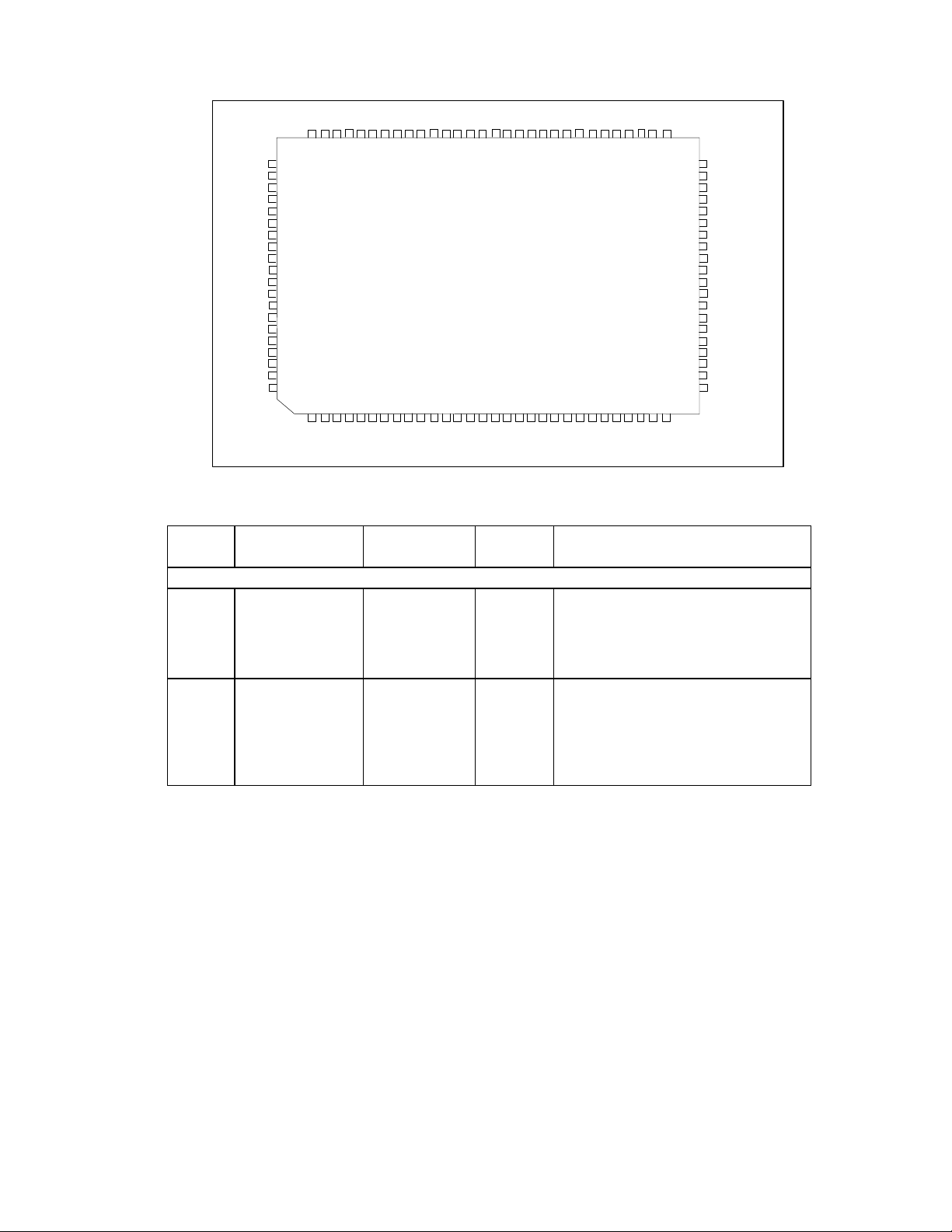
PIN CONFIGURATION
SD0
SD15
SD14
SD13
SD12
SD11
SD10
SD9
SD8
GND
VCC
SD7
SD6
SD5
SD4
SD3
SD2
SD1
MA9
MA8
GND
VCC
SA7
SA6
SA4
SA3
SA2
SA1
SA0
SA5
HSLCT
nPSTB
HPE
nPALF
HBSY
nPERR
nHACK
nPINIT
GND
VCC
HD7
HD5
HD4
HD3
nHSEL
HD2
nPACK
nHINIT
GND
VCC
HD1
PBSY
HD0
PPE
nHALF
nHSTB
nHERR
PSLCT
HD6
nPSEL
515253545556575859606162636465666768697071727374757677787980
81
nIO16
IN0
IN1
nCS0
nCS1
nCS2
nCS3
nSRD
nSWR
VCC
GND
nRAS
nCAS
nSRST
SRST
XIN(SCLK)
XOUT
BCLK
N/C
TEST
100
82
83
84
85
86
87
88
89
90
91
92
93
94
95
96
97
98
99
PPC34C60
50
nPID
49
SLCTD
48
IRQ
47
DREQ
46
TC
45
nDACK
44
nST0
43
nST1
42
nST2
41
VCC
40
GND
39
nWDOGEN
38
PIEZO
37
IN2
36
IN3
35
nLBAT
34
nRESET
33
SENSE
32
YIN
31
YOUT
302928272625242322212019181716151413121110987654321
DESCRIPTION OF PIN FUNCTIONS
BUFFER
PIN NO. NAME SYMBOL
PARALLEL PORT HOST CONTROL AND COMMON DATA BUS INTERFACE
2 nHost:Strobe nHSTB I,PU An active low pulse on this input is used
3 nHost:Auto Line
nHALF I,PU This input goes low to cause the printer
Feed
TYPE
DESCRIPTION
to strobe printer data into the printer.
Refer to Section 4 of the IEEE STD 1284
(Reference 1) for use of this pin in ECP
and EPP modes.
to automatically feed one line after each
line is printed. Connects to AUTOFD
output from Host. Refer to Section 4 of
the IEEE STD 1284 (Reference 1) for use
of this pin in ECP and EPP modes.

4
DESCRIPTION OF PIN FUNCTIONS
BUFFER
PIN NO. NAME SYMBOL
14 nHost:SelectIn nHSEL I This active low input is driven by the host
11 nHost:Initiate nHINIT I This active low input initiates the printer
24 nHost:
Acknowledge
26 Host:Busy HBSY O16 This status output, generated by the
28 Host:Paper End HPE O16 This status output, generated by the
nHACK O16 This active low output from the printer is
TYPE
DESCRIPTION
to select the printer. Connects to
SELECT IN output from Host. Refer to
Section 4 of the IEEE STD 1284
(Reference 1) for use of this pin in ECP
and EPP modes. (See Note 1 on Page
11.)
when low. Connects to INIT output from
Host. Refer to Section 4 of the IEEE
STD 1284 (Reference 1) for use of this
pin in ECP and EPP modes. (See Note 1
on Page 11.)
used to indicate that the printer has
received the data and is ready to accept
new data. Connects to the ACK input to
the Host. Refer to Section 4 of the IEEE
STD 1284 (Reference 1) for use of this
pin in ECP and EPP modes.
printer, goes high to indicate that it is not
ready to receive new data from the host.
Connects to the BUSY input to the Host.
Refer to Section 4 of the IEEE STD 1284
(Reference 1) for use of this pin in ECP
and EPP modes.
printer, goes high to indicate that the
printer is out of paper. Connects to the
PERROR input to the Host. Refer to
Section 4 of the IEEE STD 1284
(Reference 1) for use of this pin in ECP
and EPP modes.

5
DESCRIPTION OF PIN FUNCTIONS
BUFFER
PIN NO. NAME SYMBOL
30 Host:Printer
Selected
6 nHost:Printer Error nHERR O16 This status output, generated by the
5,8,13,15
-18, 20
Host:Data[0:7] HD[0:7] I/O16,PUParallel port bi-directional data bus
PARALLEL PORT PASS-THROUGH INTERFACE PINS
29 nPass-Through:
Strobe
27 nPass-Through:
Auto Line Feed
HSLCT O16 This status output, generated by the
nPSTB O16 An active low pulse on this output is used
nPALF O16 This output goes low to cause the printer
TYPE
DESCRIPTION
printer, goes high to indicate that the
printer is selected. Connects to the
SELECT input to the Host. Refer to
Section 4 of the IEEE STD 1284
(Reference 1) for use of this pin in ECP
and EPP modes.
printer, goes low to indicate an error
condition at the printer. Connects to the
ERROR input to the Host. Refer to
Section 4 of the IEEE STD 1284
(Reference 1) for use of this pin in ECP
and EPP modes.
connected to host system is used by
SPP, ECP and EPP to transfer data
between the host CPU and peripherals.
Refer to Section 4 of the IEEE STD 1284
(Reference 1) for use of this pin in ECP
and EPP modes.
to strobe printer data into the printer.
Connects to the STROBE input on the
next device along the chain. Refer to
Section 4 of the IEEE STD 1284
(Reference 1) for use of this pin in ECP
and EPP modes.
to automatically feed one line after each
line is printed. Connects to the AUTOFD
input on the next device along the chain.
Refer to Section 4 of the IEEE STD 1284
(Reference 1) for use of this pin in ECP
and EPP modes.

6
DESCRIPTION OF PIN FUNCTIONS
PIN NO. NAME SYMBOL
19 nPass-Through:
SelectIn
23 nPass-Through:
Initiate
12 nPass-Through:
Acknowledge
7 Pass-Through:
Busy
4 Pass-Through:
Paper End
nPSEL O16 This active low output selects the printer.
nPINIT O16 This active low output initiates the printer
nPACK I, PU This active low input from the printer is
PBSY I, PU This status input, generated by the printer
PPE I, PU This status input, generated by the
BUFFER
TYPE
DESCRIPTION
Connects to the SELECT IN input on the
next device along the chain. Refer to
Section 4 of the IEEE STD 1284
(Reference 1) for use of this pin in ECP
and EPP modes.
when low. Connects to the INIT input on
the next device along the chain. Refer to
Section 4 of the IEEE STD 1284
(Reference 1) for use of this pin in ECP
and EPP modes.
used to indicate that the printer has
received the data and is ready to accept
new data. Connects to the ACK output
from the next device along the chain.
Refer to Section 4 of the IEEE STD 1284
(Reference 1) for use of this pin in ECP
and EPP modes.
goes high to indicate that it is not ready
to receive new data from the PassThrough. Connects to the BUSY output
from the next device along the chain.
Refer to Section 4 of the IEEE STD 1284
(Reference 1) for use of this pin in
ECP/EPP modes.
printer, goes high to indicate that the
printer is out of paper. Connects to the
PERROR output from the next device
along the chain. Refer to Section 4 of the
IEEE STD 1284 (Reference 1) for use of
this pin in ECP and EPP modes.

7
DESCRIPTION OF PIN FUNCTIONS
BUFFER
PIN NO. NAME SYMBOL
1 Pass-Through:
Printer Selected
25 nPass-Through:
Printer Error
SYSTEM (REGENERATED ISA PERIPHERAL) INTERFACE
96
System
Clock/Crystal
97
80-73 System Address
[0:7]
70,69 Memory Address
[8,9]
68-61,
58-51
System Data [0:15] SD[0:15] I/O8,PUThese bi-directional pins are used to
88 nSystem Read nSRD O8 This indicates that a bus read cycle is
PSLCT I, PU This status input, generated by the
nPERR I, PU This status output, generated by the
XIN (SCLK)
XOUT
SA[0:7] O8 These lower eight address bits are
MA[8:9] O8 These address bits are appended to
TYPE
I
O8
DESCRIPTION
printer, goes high to indicate that the
printer is selected. Connects to the
SELECT output from the next device
along the chain. Refer to Section 4 of the
IEEE STD 1284 (Reference 1) for use of
this pin in ECP/EPP modes.
printer, goes low to indicate an error
condition at the printer. Connects to the
ERROR output from the next device
along the chain. Refer to Section 4 of the
IEEE STD 1284 (Reference 1) for use of
this pin in ECP and EPP modes.
XIN may be connected to a ttl peripheral
system clock or a crystal may be placed
across XIN/XOUT (typically 24MHz).
This is used to derive the internal clock
(BUSCLK) used for all system interface
timing.
presented to the system bus directly by
the PPC34C60 during bus and DRAM
access. Upper address bits, if needed,
should be latched through use of the
PPC34C60's strobe lines prior to
generating bus accesses.
SA[0:7] to create a 10-bit row or column
address for DRAM access.
transfer data during bus or DRAM cycles
to or from the system.
occurring, similar to an ISA MEMR
signal.

8
DESCRIPTION OF PIN FUNCTIONS
BUFFER
PIN NO. NAME SYMBOL
89 nSystem Write nSWR O8 This indicates that a bus write cycle is
81 n16-Bit I/O nIO16 I, PU This signal is asserted by the remote
48 Interrupt Request IRQ I, PU This rising edge activated signal indicates
94 nSystem Reset nSRST O8 This low going signal can be used to
95 System Reset SRST O8 This high going signal can be used to
92 nRow Address
Strobe
93 nColumn Address
Strobe
45 nDMA
Acknowledge
46 Terminal Count TC O8 This active high output is asserted with
nRAS O8 This low going strobe signal is used by
nCAS O8 This low going strobe signal is used by
nDACK O8 This active low output signal is issued to
TYPE
DESCRIPTION
occurring, similar to an ISA MEMW
signal.
system to indicate whether or not the
address being accessed is capable of a
16-bit transfer.
an interrupt request from the System.
reset the System. This signal is asserted
for 16 SCLKs.
reset the System. This signal is asserted
for 16 SCLKs.
the DRAM to latch the row address,
present on the SA[0:7] and MA[8:9] pins.
This output drives the DRAM directly,
however a series resistor is
recommended on this line.
the DRAM to latch the column address,
present on the SA[0:7] and MA[8:9] pins.
This output drives the DRAM directly,
however a series resistor is
recommended on this line.
inform the System that data is to be
transferred using DMA transfer cycles.
the last DMA data transfer to indicate to
the System that the DMA data transfer is
complete. TC is asserted in conjunction
with DACK.

9
DESCRIPTION OF PIN FUNCTIONS
BUFFER
PIN NO. NAME SYMBOL
47 DMA Request DREQ I, PD The remote system indicates that it is
MISCELLANEOUS
39 nWatchdog Enable nWDOGEN I, PU Pulling this line low enables the
34 nReset Chip nRESET I, PU Pulling this line low for two SYSCLKs will
35 nLow Battery
Indicator
82,83,
37,36
44,43, 42 nStrobes[0:2]
General Purpose
Inputs [0:3]
38 Piezo Crystal Drive PIEZO O24 This high current output can be directly
(special function)
nLBAT I, PU A low level on this input line signals that
IN[0:3] I, PU The host may obtain the level at these
nST[0:2] O8 These pins are individually configured as
TYPE
DESCRIPTION
ready to perform DMA transfers by
driving this line high. This signal is
asserted as long as the System is ready
to receive or send data and is deasserted
on the last byte of the data transfer.
watchdog. The watchdog will generate
four beeps on the piezo driver if there are
no transitions on the host port lines for a
minute. This circuitry can also
automatically power down the system
when the watchdog "barks". This feature
requires software to tickle the port every
30 seconds.
reset the PPC34C60 to its initial state.
This will reset all internal registers to their
default values.
the battery power is low and the
PPC34C60 will generate low battery
tones. It is the responsibility of the
remote system to monitor battery power
and generate this input signal.
pins by reading the Internal Input
Register.
hooked up to a piezo speaker to provide
audio tones.
general purpose outputs or as strobe
outputs as programmed in the Output
Configuration Register. ST2 may also be
programmed as the Auto-Power pin.

10
DESCRIPTION OF PIN FUNCTIONS
BUFFER
PIN NO. NAME SYMBOL
84-87 nChip Selects[0:3]
(special function)
32
Oscillator Input
31
Oscillator Output
49 Selected Device SLCTD O8 This signal is an active high output that
50 nProduct ID PID O8 This signal is an active low output
33 Sense VCC SENSE I, PD When pulled high, this input will enable
nCS[0:3] O8 These pins are individually configured as
YIN
YOUT
TYPE
I
08
DESCRIPTION
general purpose outputs or as chip select
outputs as programmed in the Output
Configuration Register.
A parallel resonant crystal or RC network
may be placed across YIN and YOUT.
This nominal 32KHz clock (32.768KHz)
is used by the internal piezo driver and
watchdog timer.
indicates that the device is the active
device on the daisy chain. This may be
used for debug purposes, to enable
drivers, or to qualify signals.
asserted when the host performs a
request for the peripheral's Product ID.
This function is used by the daisy chain
and multiplexor protocols.
all output drivers of the PPC34C60.
When low, all outputs are tri-stated. This
resolves the back-power problem
inherent in parallel port peripherals.
Isolate the chip's VCC from the rest of
the peripheral's VCC using a schottky
diode. The SENSE input should be tied
to the peripheral's VCC and the anode of
the diode. In this manner, when the
peripheral's power is off, the sense input
will shut down all outputs, preventing the
chip from driving into a low impedance
load and consequently damaging the
chip's input protection diodes.

11
DESCRIPTION OF PIN FUNCTIONS
BUFFER
PIN NO. NAME SYMBOL
100 Test Counters TEST I, PD This is an active high signal that allows
98 BUSCLK BCLK O8 BUSCLK is the SCLK divided by the
99 Reserved RESERVED Leave floating, no connection
9,21,
41,60,
72,90
10,22,
40,59,
71,91
Note 1: By pulling both these lines low (illegal state), the PPC34C60's output ports can be disabled.
Power VCC +5 Volt supply pins.
Ground GND Ground pins
TYPE
DESCRIPTION
access to some large counter chains that
are normally buried within the chip. For
normal operation this input should be left
unconnected, or tied to ground. For
more information on the test mode
contact the factory.
value programmed in the Configuration
Register.

12
BUFFER TYPE DESCRIPTIONS
BUFFER TYPE DESCRIPTION
I
I/O8
I/O16
O8
O16
O24
PU
PD
Input, Schmitt Trigger
Input, Schmitt Trigger/8mA Output
Input, Schmitt Trigger/16mA Output
8mA Output
16mA Output
24mA Output
Pull Up, nominal 100K
Pull Down, nominal 100K
GENERAL CONVENTIONS
Throughout this document, the following various terms and conventions will be used:
Compatible = "Centronics"
SPP = "Standard Bi-Directional Parallel Port" (PS/2)
EPP = "Enhanced Parallel Port"
ECP = "Extended Capabilities Port"
REFERENCE DOCUMENTS
1. IEEE STD 1284, February 2, 1993.
2. The Enhanced Parallel Port, an Introduction; FarPoint Communications.
3. Daisy Chain Specification, Rev. 1.1, September 16, 1993; Disctec Corporation.
4. Enhanced Parallel Port BIOS Specification, Rev 3, February 12, 1993; FarPoint Communications.
5. ECP: Specification Kit, Rev 1.03, February 10, 1993; Microsoft Corporation.
13
FUNCTIONAL DESCRIPTION
PPC34C60 BLOCK DESCRIPTION
The PPC34C60 can be broken down into eight
functional blocks as shown in Figure 1.
The PPC34C60 implements and complies with the
Daisy Chain Specification (Reference 3) through
the Daisy Chain Protocol block. Under the Daisy
Chain protocol, the PPC34C60 operates in either
Pass-Through or Selected mode. Pass-Through
mode is the power up default, and is electrically
transparent to devices further down the chain.
When in Pass-Through mode, the Data Switch
gates the control and status lines of the parallel
port to the Pass-Through port. Selected mode
connects the System Interface bus to the parallel
port. When in Selected mode, the Data Switch
gates the control and status lines to the
PPC34C60's Protocol Translator functional block.
Daisy
Chain
Protocol
Protocol
nHSTB
nHALF
nHSEL
nHINIT
nHACK
HBSY
HPE
HSLCT
nHERR
HD[0:7]
nPSTB
nPALF
nPSEL
nPINIT
nPACK
PBSY
PSLCT
nPERR
HD[0:7]
PPE
Host
Parallel
Port
Pass-Through
Port
Data
Switch
Translator
SPP
EPP
ECP
SLCTD
nRESET
SENSE
TEST
The Protocol Translator block gives the PPC34C60
its capability to communicate with the parallel port
in either SPP, EPP, or ECP mode. The Protocol
Translator interprets the Multiport Access Protocol
(MAP) packets described in the Daisy Chain
Specification (Reference 3). The MAP packets and
command codes are described in the Daisy Chain
Command Protocol. The Protocol Translator also
decodes the type of parallel port transfer (ie.
Address Write/Data Read_Write Cycle) and
provides the proper control of the data to the
Registers and Control block and to the Bus
Interface block. The PPC34C60's internal registers,
contained in the Register and Control block, control
the operation of the chip's internal DRAM
Controller, DMA Controller, and Watchdog
Controller. The Bus Interface block controls data
transfers between the Parallel Port and the
peripheral's System Interface Bus. The MUX block
routes data and control signals to the System
Interface
A_STB
B_STB
.
Registers
and
Control
Bus
Interface
DRAM
Controller
DMA
Controller
WDOG
& Piezo
Counters
MUX
SPEAKER
SYSTEM
INTERFACE
SA[0:7]
MA[8:9]
SD[0:15]
nSRD
nSWR
nIO16
IRQ
nLBAT
YIN, YOUT,
nWDOGEN, PIEZO
XIN, XOUT
nDACK
TC
nST[0:2]
DREQ
nCS[0:3]
nRAS
nCAS
nDIR
nPID
IN[0:3]
SRST
nSRST
FIGURE 1 – INTERNAL BLOCK DIAGRAM

14
DAISY CHAIN COMMAND PROTOCOL
The daisy chain protocol is used to select the mode
of each device and to allow connection of up to
eight devices on one parallel port. The daisy chain
commands use the Multiport Access
Protocol (MAP) to access the devices. The
format of the MAP packets is as follows:
The command byte in the MAP packet represents a
code and possibly an address as well. The
currently defined codes are:
(00-07)
(08-0F)
(10-17)
(20-27)
(30)
(40)
(48)
(50-57)
(58-5F)
(D0-D7)
(E0-E7)
0000 0aaa
0000 1aaa
0001 0aaa
0010 0aaa
0011 xxxx
0100 0xxx
0100 1xxx
0101 0aaa
0101 1aaa
1101 0aaa
1110 0aaa
Assign address aaa to the current device
Query Interrupt from device aaa
Query Product ID from device aaa
Select device aaa in EPP mode
De-select all devices
Disable Daisy Chain Interrupts
Enable Daisy Chain Interrupts
Clear Interrupt Latches on device aaa
Set Interrupt Latch on device aaa
Select device aaa in ECP mode
Select device aaa in Compatible Mode - SPP
aaa = Device Address
xxx = Undefined - set to zero
Refer to the Daisy Chain Specification (Reference 3) for more information.
15
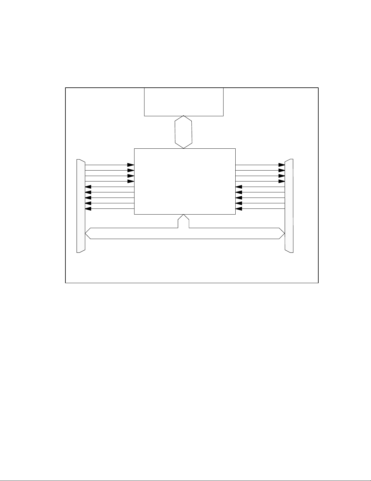
PERIPHERAL SYSTEM DESIGN
Connector
Connector
The PPC34C60 simplifies the design of a
peripheral to exploit the benefits of IEEE STD 1284,
Standard Signaling for a Bi-Directional Parallel Port
(Reference 1). Figure 2 depicts a high-level
System Block Diagram which shows the peripheral
chip's three primary data paths.
ISA Peripheral
System
nHSTB
nHALF
H
O
S
T
nHSEL
nHINIT
nHACK
HBSY
HPE
HSLCT
nHERR
Interface
PPC34C60
P
O
R
T
Parallel Port Data Bus
Note that the Parallel Port Data Bus is not switched
through the PPC34C60; this allows all daisy
chained devices to receive a special "out of band"
Control Packet as defined in the Distec Daisy
Chain Specification (Reference 3).
nPSTB
nPALF
nPSEL
nPINIT
nPACK
PBSY
PPE
PSLCT
nPERR
P
A
S
S
T
H
R
U
Host
Parallel Port
Pass-Through
Parallel Port
FIGURE 2 – SYTEM BLOCK DIAGRAM
16
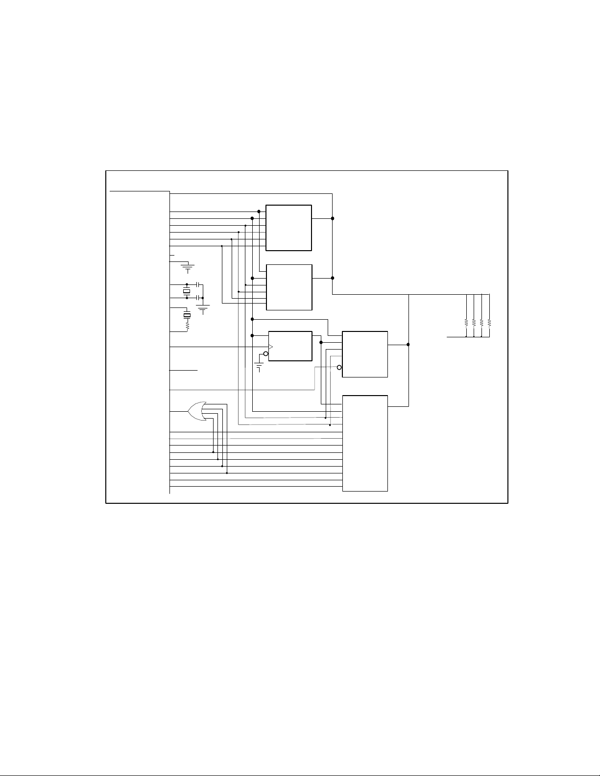
DESIGN EXAMPLE
SD0
SD5
SD10
SD15
Figure 3 shows a simple system design that uses
most of the PPC34C60's interface functions. This
example shows:
1) A DRAM interface.
2) An 8Kx8 NV-memory device interface using
nStrobe Output 0 to latch the upper address
bits and nChip Select Output 0 to enable the
device.
PPC34C60
SD[0:15]
MA[8:9]
SA[0:7]
nSWR
nSRD
nRAS
nCAS
nIO16
TEST
Xout
Yout
nST0
nPID
nCS0
IRQ
DREQ
nDACK
CS1
SRST
Xin
Yin
IN0
IN1
IN2
IN3
24MHz
32
KHz
nPID
TC
1Mx8 DRAM
A[8:9]
A[0:7]
nWR
nOE
nRAS
nCAS
1Mx8 DRAM
A[8:9]
A[0:7]
SD[8:15]
nWR
nOE
nRAS
nCAS
374
D[0:7]
CLOCK
nOE
UPPER
ADDRESS
LATCH
3) An interface to SMSC's FDC37C662 Super I/O
Floppy Disk Controller. This section of the
design illustrates how the PPC34C60 can
handle a direct memory access interface, four
interrupts, and an additional chip select output
configured as a standard output pin. The
SRST (reset output) is used to reset the floppy
disk controller.
4) The use of 10K bias resistors to implement a
product ID code.
SD[0:7]
Optional, 8Kx8 SRAM
EEPROM, etc.
Q[0:7]
A[0:7]
A[8:12]
SD[0:7]
nWR
nOE
nCE
FDC37C662
D[0:7]
A[8:9]
A[0:7]
nIOW
nIOR
FDRQ
nDACK
TC
IRQ3
IRQ4
PINTR
FINTR
AEN
RST
nPID
Product
7BDEh
ID =
FIGURE 3 – TYPICAL SYSTEM INTERFACE
17
DEVICE ADDRESSING
The Bi-Directional Parallel Peripheral Interface
protocol, defined by the IEEE STD 1284
(Reference 1), describes two basic types of 8-bit
information transfers: data read/write operations
and address read/write operations. The
PPC34C60's bus and internal registers are
accessed via data read/write operations.
Table 1 - Key Address/Data Cycle Signals
SIGNAL SPP EPP ECP
Address
Strobe
Data
Strobe
Reverse Channel
Signal
SEL SEL STB(ALF=0)
STB ALF STB(ALF=1)
INIT=0 IMPLICIT INIT = 0
The PPC34C60's address mode is set through an
SPP, EPP, or ECP address write operation. Table
1 specifies the control signals used by each
protocol to perform Address and Data Cycles and
to indicate reverse data flow. Refer to the IEEE
STD 1284 (Reference 1) for further information.
The Parallel Port provides a byte-wide parallel data
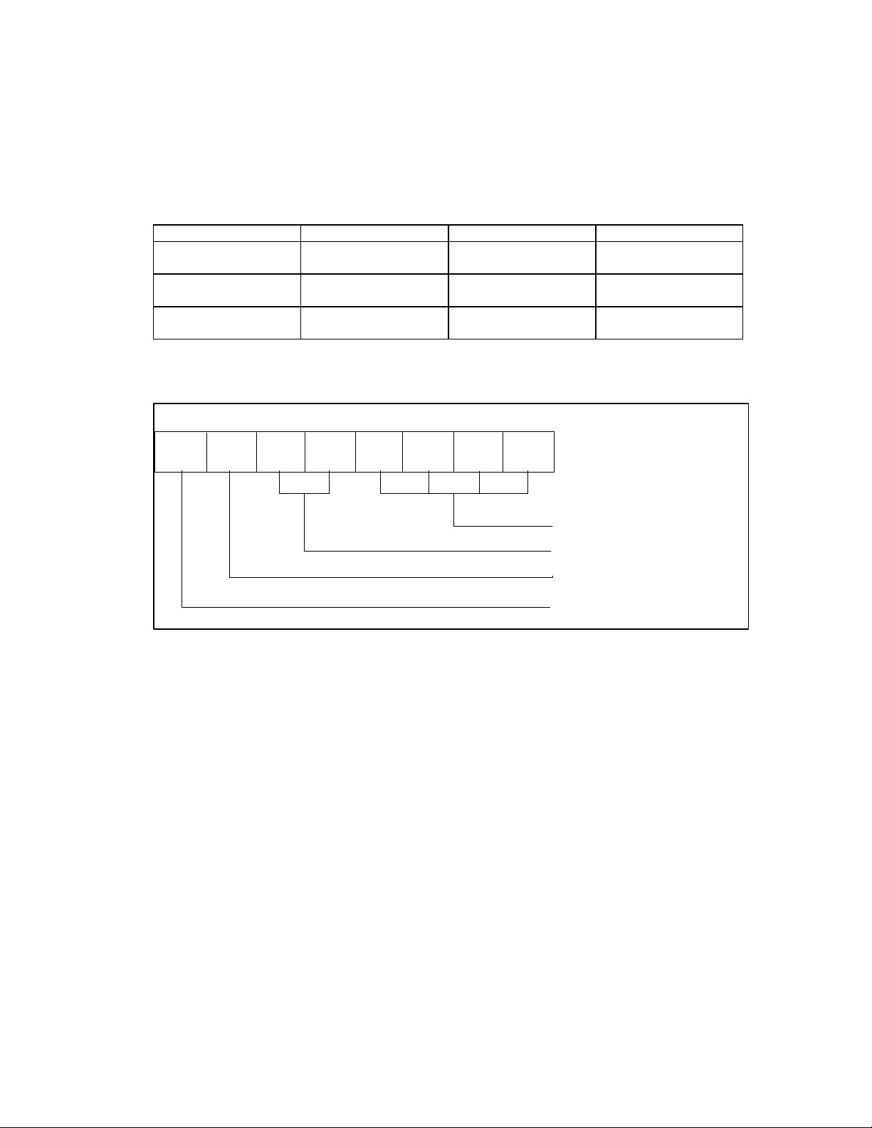
path. Figure 4 defines the data bits of
this parallel port data path during an address write
operation to the PPC34C60.
D7 D5 D4 D3D6 D2 D1 D0
1 B M AW A A A
FIGURE 4 – PARALLEL PORT ADDRESS WRITE AND DATA BITS
Bus or Register Address
Type of Access
Write/Read
Required for ECP

18
An address write cycle is used to select the
PPC34C60's address mode for subsequent data
write cycles. Table 2 shows ten types of Address
Modes into which the PPC34C60 may be placed.
The address write data byte required for each
mode is encoded as '1WBMA3A2A1A0'.
Unrestricted System Data Bus access can also
occur following Address Write operations where
1WBMA3A2A1A0 = 1X00(A3-A0), except that in
this short hand addressing mode A3-A0 is also
written to the least significant four bits of the
PPC34C60 internal Address Register. Address
Write operations where 1WBMA3A2A1A0 =
Table 2 also illustrates three separate System Data
Bus addressing modes along with DRAM and
1X01(A3-A0) provides block count limited System
Data Bus access with shorthand addressing.
Internal Registers addressing.
For example, an Address Write operation in which
When the Host Address Write data is 1X100XXX,
the PPC34C60 provides unrestricted System Data
Bus access for all subsequent Host Parallel Port
B = 1, M = 0, and A3A2A1A0 = 0000 selects
System Data Bus access but does not alter the
value of the PPC34C60 Address Bus, SA[0:7].
data exchanges.
Table 2 - Address Mode Operations
1WBM A3A2A1A0 Access Type W=1(Write) W=0(Read)
1X00 (A3-A0)
Unrestricted Bus Write
(Shorthand Mode)
Unrestricted Bus Read
(Shorthand Mode)
SYSTEM DATA
BUS
1X01 (A3-A0) Block Restricted Bus
Write (Shorthand Mode)
1X10 0XXX (BUS) Unrestricted Bus Write
Access
1X10 1XXX
DRAM DRAM Write Access DRAM Read Access
Block Restricted Bus
Read (Shorthand Mode)
Unrestricted Bus Read
Access
(DRAM)
1X11 RRRR INTERNAL
REGISTERS
Write Internal Register
RRRR
Read Internal Register
RRRR
W = Write
B = Bus
M = Max Count
A3A2A1A0 = Address Selector
RRRR = Register Selector

19
INTERNAL REGISTER MAP
The internal registers of the PPC34C60 are
selected by performing an Address Write Cycle
with bits B and M (bits 5 and 4) set to 1,1 (see
Table 2). The desired register is selected by
Table 3 - Internal Register Map
W* BM RRRR REGISTER DESCRIPTION DEFAULTS
X 11 0000 Address Register 00
X 11 0001 Output Configuration Reg 10
X 11 0010 Output Register 80
1 11 0011 Sound Register NA
0 11 0011 Input Register SF
X 11 0100 Operation Register 00
X 11 0101 DRAM Buffer Size Register 0C
X 11 0110 Host DRAM Buffer Pointer 00
X 11 0111 DMA DRAM Buffer Pointer 00
X 11 1000 Host Max Block Count - Low 00
X 11 1001 Host Max Block Count - High 10
X 11 1010 DMA Byte Count - Low 00
X 11 1011 DMA Byte Count - High 00
X 11 1100 Configuration Register 04
0 11 1101 Chip Revision Level 00
1 11 1110 Port Test Register NA
0 11 1110 Port Test Register 00
X 11 1111 Data Transfer Control Register 01
the binary value of A3A2A1A0 (bits-3:0), also
shown as RRRR. Internal register RRRR is made
available for Read or Write based on the bit value
of W (bit 6) as shown below. All internal registers
are eight bits wide.
*W
X = Read/Write
1 = Write
0 = Read

20
REGISTER DESCRIPTIONS
ADDRESS REGISTER - 0000 (Read/Write)
The value in the Address Register represents the
current address presented to the Bus Address lines
SA[0:7]. The primary method of updating this
value is the following sequence. First the Address
Register is selected to be written to by performing
an Address Write operation
(XWBMA3A2A1A0=x1110000). Next a Data Write
operation is issued to write A<0:7> as a group
equal to the value presented on the parallel port
host data lines HD[0:7].
A shorthand mode is also provided to allow the
Address to be modified and Bus Operation to be
selected in one Address Write operation. If B = 0,
then bus operation is selected and A3A2A1A0 is
written to A<0-3>; A<4-7> are unaffected. In this
mode, if M = 1, then the bus access will be limited
by the Host Max Block Count Register. Any
attempts to read more data will return invalid data.
The PPC34C60 contains an integrated FIFO to
enhance performance by reading the Bus one or
two bytes ahead of the Host Port. As an example,
some devices such as IDE hard drives expect data
to be read in a fixed block length (sector). Set
MAXCNT (Configuration Register bit 6) and set the
value of Host Max Block Count Register to the
length of the IDE data block to read only the
desired amount of data (1 sector) from the
peripheral.
If M = 0, then the current setting of MAXCNT and
Host Max Block Count are ignored. This allows
polling of a status register without limiting the
number of times the register may be accessed.
The PPC34C60 directly provides eight address
lines. If more than eight bits of address are
necessary, three strobe lines are available which
may be used with external circuitry to latch
higher-order address bits off of SA[0:7]. For
example, the address register can be written with
higher order address bits and latched with one or
more of the three programmable strobe lines. The
address register is then written with A0-A7, and
normal bus reads/writes follow. This scheme may
be extended to any size address bus needed.
An auto-increment option may be activated by
setting AUTOINC (bit 4 in the Operation Register,
RRRR=0100) which will increment A<0:7> after
each bus access.
21
OUTPUT CONFIGURATION REGISTER - 0001 (Read/Write)
Bit 7 Bit 6 Bit 5 Bit 4 Bit 3 Bit 2 Bit 1 Bit 0
SP1 SP0 SO1 SO0 CO3 CO2 CO1 CO0
The Output Configuration Register defines the
operation of the bits in the Output Register.
The PPC34C60 has eight independent output lines.
The functionality of seven of these output lines is
selected through the Output Configuration Register.
All eight output lines are then controlled or
activated through the Output Register
(RRRR=0010).
The seven programmable output lines controlled by
Output Register bits 0-6 can be selected to
Bits 0-3:
SPECIAL FUNCTIONS FOR PROGRAMMABLE
OUTPUT LINES 0-3:
Programmable output lines 0-3 can be individually
configured as General Purpose (inverting) outputs
or as chip select outputs. Chip selects are
generated by the bus cycle state machine.
During a bus cycle, the chip select goes low at the
start of the cycle and remains low until the end of
the cycle.
operate as either general purpose output
pins (inverting), or as special function output pins.
The special functions are: Chip Select, Strobe, and
Auto-Power.
The eighth (non-programmable) output line is
controlled by Output Register bit 7. This output line
is defined as "Bus Reset", but it is simply an output
bit. It may be used for other purposes if a Bus
Reset signal is not required or generated
elsewhere. This bit is present on two pins (95 and
94) in both normal and inverted polarities.
Output line N (N = 0...3) is controlled through
Output Register Bit N. Output line N, configured as
a General Purpose output, will present the inverted
value written to Output Register bit N. Output line
N, configured as a Chip Select, will follow the bus
chip select if Output Register bit N is a 1.
Bit 0:CO0 - Chip Select 0/Standard Output 0
0 Select Output line 0 (Pin 84) as a General Purpose inverting output.
1 Select Output line 0 (Pin 84) as a Chip Select output.
Bit 1:CO1 - Chip Select 1/Standard Output 1
0 Select Output line 1 (Pin 85) as a General Purpose inverting output.
1 Select Output line 1 (Pin 85) as a Chip Select output.

22
Bit 2:CO2 - Chip Select 2/Standard Output 2
0 Select Output line 2 (Pin 86) as a General Purpose inverting output.
1 Select Output line 2 (Pin 86) as a Chip Select output.
Bit 3:CO3 - Chip Select 3/Standard Output 3
0 Select Output line 3 (Pin 87) as a General Purpose inverting output.
1 Select Output line 3 (Pin 87) as a Chip Select output.
Bits 4-7:
SPECIAL FUNCTIONS FOR PROGRAMMABLE
OUTPUT LINES 4-6
Programmable Output lines 4-6 can be individually
configured as general purpose (inverting) outputs
or as strobe outputs. These strobe signals may be
used to clock any edge-triggered flip-flop or
register. Additionally, Programmable Output line 6
may be programmed as an Auto-Power pin. This
signal allows a peripheral to automatically control
Bit 4:SO0 - Strobe 0/Standard Output 4
0 Select Output line 4 (Pin 44) as a General Purpose inverting output.
1 Select Output line 4 (Pin 44) as a Strobe output.
its power on state, so that a separate power switch
is not necessary. The external circuitry necessary
for this passively pulls down the INIT line from the
host. The power supply is turned on when the INIT
line rises to a high logic level. The PPC34C60 will
then monitor the host, and will bring the AutoPower pin to a logic low level when the power can
be shut off.
Output line N, configured as a Strobe signal, is
normally high and pulses low momentarily when a
1 is written to Output Register bit N.
Bit 5:SO1 - Strobe 1/Standard Output 5
0 Select Output line 5 (Pin 43) as a General Purpose inverting output.
1 Select Output line 5 (Pin 43) as a Strobe output.
Bit 6,7:SP0,SP1 - Auto-Power/Strobe 2/Standard Output 6
0,x Select Output line 6 (Pin 42) as an Auto-Power Pin.
1,0 Select Output line 6 (Pin 42) as a General Purpose inverting output.
1,1 Select Output line 6 (Pin 42) as a Strobe output.

23
OUTPUT REGISTER - 0010 (Read/Write)
Bit 7 Bit 6 Bit 5 Bit 4 Bit 3 Bit 2 Bit 1 Bit 0
BRESET nOP6
nPWR
nOP5
STB1
nOP4
STB0
nOP3
CS3
nOP2
CS2
nOP1
CS1
STB2
nOP0
CS0
Each Output Register bit independently controls the
operation of its respective Output pin. The function
of each output pin, except for BRST (Pins 94 and
95), is determined by the data stored in the Output
Configuration Register.
CHIP SELECT OUTPUTS
Output lines 0-3 (Pins 84-87) are programmable as
Chip Selects (CS0-CS3) via the Output
Configuration Register. When programmed as a
Chip Select, the output pin will go low during bus
operations if its associated bit in the Output
Register is set. If the associated bit is not set in
this register, the output pin will remain high.
STROBE OUTPUTS
Output lines 4-6 (Pins 44-42), when programmed
as strobes (STB0-STB2) via the Output
Configuration Register, will pulse low for two
BUSCLK periods when the associated bit is set.
The strobes recover and may be re-written at any
time. Note: the strobe Output Register bits are
reset automatically after the strobe is generated.
AUTO-POWER OUTPUT
Output line 6 (Pin 42), when programmed as
Auto-Power (nPWR), via the Output Configuration
Register, will remain at a high level as long as host
activity is detected. When the chip determines that
power may be shut off, this pin will go low.
There are two mechanisms driving this output. The
first mechanism monitors the levels on the host
port. If the port assumes the terminated levels or
all low levels for 16 to 20 seconds, then the host is
presumed off (or disconnected). The second
mechanism monitors Host port activity (signal
transitions). After a one minute period of inactivity
(given that the WDOGEN pin is tied low) the
watchdog will be triggered sending four beeps to
the piezo driver. After completion of the tones the
Auto-Power pin will go low.
GENERAL PURPOSE OUTPUTS
Bit 7 (BRESET) and any other bits that are
programmed through the Output Configuration
Register as general purpose output bits are
inverted and passed to the associated output pin.
 Loading...