

SMSC MON35W82 Datasheet

MON35W82
Hardware Monitoring IC – I2C Interface Only
FEATURES
• Monitoring Items
- 3 Thermal Inputs From Remote
Thermistors or 2N3904 NPN-type
Transistors or PentiumTM II
(Deschutes) thermal diode output
- 6 Voltage Inputs
Typical for Vcore, +3.3V, +12V,
-12V, +5V, -5V (Optional)
- 3 Fan Speed Monitoring Inputs
- WATCHDOG™ Comparison of all
Monitored Values
- Programmable Hysteresis and Setting
Points (Alarm Thresholds) for all
Monitored Items
• Actions Enabling
- Beep Tone Warning
- 2 PWM (Pulse Width Modulation)
Outputs for Fan Speed Control (MUX
Optional)
- Total up to 2 Sets of Fan Speed
Monitoring and Controlling.
- Issues nSMI, nOVT and nGPO Signals
to Activate System Protection
- Warning Signal Pop-Up in Application
Software
• General
- I2CTM Serial Bus Interface
- 5 VID Input Pins for CUP Vcore
Identification (for PentiumTM II)
- Initial Power Fault Beep (for +3.3V,
Vcore)
- IntelTM LDCM (DMI Driver 2.0) Support
- AcerTM ADM (DMI Driver 2.0) Support
- Input Clock Rate Optional for 24, 48,
and 14.318 MHz
- 5V Vcc Operation
• Package
- 24 Pin SOP
GENERAL DESCRIPTION
The MON35W82 is an enhanced version of the
MON35W42. The MON35W82 can be used to
monitor several critical hardware parameters of
the system, including power supply voltages, fan
speeds, and temperatures, which are very
important for proper operation and stability of a
high-end computer system. The MON35W82
provides an I2CTM serial bus interface.
An 8-bit analog-to-digital converter (ADC) is
contained inside the MON35W82. The
MON35W82 can monitor 6 analog voltage
inputs, 3 fan tachometer inputs, and 3 remote
temperatures. The remote temperature sensing
can be performed by thermistors, 2N3904 NPNtype transistors, or directly from Intel’s
TM
Deschutes CPU thermal diode output. The
MON35W82 also provides: 2 PWM (pulse width
modulation) outputs for the fan speed control;
beep tone output for warning; nSMI, nOVT, and
nGPO signals for system protection events.
With application software such as the Intel™
LDCM (LAN Desk Client Management) the user

2
can read all the monitored parameters of the
system from time to time. And a pop-up
warning can be activated when the monitored
item drifts out of the proper/preset range. Also
the user can set the upper and lower limits
(alarm thresholds) of these monitored
parameters and activate programmable and
maskable interrupts. An optional beep tone
could be used as a warning signal when the
monitored parameters are out of the preset
range.
Additionally, 5 VID inputs are provided to read
the VID of the CPU (i.e. PentiumTM II) if
applicable. This will provide automatic
correction of the Vcore voltage. The
MON35W82 also uniquely provides an optional
feature: early stage (before BIOS is loaded)
beep warning. This is to detect if the fatal
elements such as Vcore or 3.3V voltage fail are
present.
Standard Microsystems is a registered trademark and
SMSC is a trademark of Standard Microsystems
Corporation. Other product and company names are
trademarks or registered trademarks of their respective
holders.
WATCHDOG is a registered trademark of National
Semiconductor Corporation.
KEY SPECIFICATIONS
• Voltage monitoring accuracy ±1% (Max)
• Monitoring Temperature Range and Accuracy
- 40°C to +120°C ± 3°C (Max)
• Supply Voltage 5V
• Operating Supply Current 5 mA typ.
• ADC Resolution 8 Bits

3
TABLE OF CONTENTS
KEY SPECIFICATIONS..................................................................................................................... 2
PIN DESCRIPTION ...........................................................................................................................6
PIN DESCRIPTION ........................................................................................................................... 7
FUNCTIONAL DESCRIPTION........................................................................................................... 8
GENERAL DESCRIPTION ............................................................................................................ 8
ACCESS INTERFACE .......................................................................................................................... 8
ANALOG INPUTS........................................................................................................................ 12
Monitor over 4.096V voltage:.................................................................................................... 13
Monitor negative voltage: ......................................................................................................... 14
Monitor temperature from thermistor:....................................................................................... 15
Monitor temperature from Pentium IITM..................................................................................... 15
FAN SPEED COUNT AND FAN SPEED CONTROL................................................................................. 16
Fan Speed Count..................................................................................................................... 16
Fan Speed Control................................................................................................................... 17
TEMPERATURE MEASUREMENT MACHINE ............................................................................................ 18
Temperature Sensor 2 Interrupt Mode...................................................................................... 19
Temperature Sensor 1 Interrupt Mode...................................................................................... 20
Temperature Sensor 1.............................................................................................................. 21
VOLTAGE AND FAN nSMI MODE ........................................................................................................ 22
Voltage nSMI mode:................................................................................................................. 22
Fan nSMI mode: ...................................................................................................................... 22
REGISTERS AND RAM .................................................................................................................. 24
CONFIGURATION REGISTER - INDEX 40H............................................................................................. 24
INTERRUPT STATUS REGISTER 1 - INDEX 41H.....................................................................................25
INTERRUPT STATUS REGISTER 2 - INDEX 42H.....................................................................................25
nSMI MASK REGISTER 1 - INDEX 43H ............................................................................................... 26
nSMI MASK REGISTER 2 - INDEX 44H ............................................................................................... 27
RESERVED REGISTER INDEX 45H-- 46H ......................................................................................... 27
VID/FAN DIVISOR REGISTER - INDEX 47H........................................................................................... 28
SERIAL BUS ADDRESS REGISTER - INDEX 48H..................................................................................... 28
VALUE RAM INDEX 20H- 3FH OR 60H - 7FH .................................................................................. 29
VOLTAGE ID (VID4) & DEVICE ID - INDEX 49H................................................................................... 31
TEMPERATURE 2 AND TEMPERATURE 3 SERIAL BUS ADDRESS REGISTER--INDEX 4AH............................... 31
PIN CONTROL REGISTER - INDEX 4BH................................................................................................ 32
nIRQ/NOVT PROPERTY SELECT - INDEX 4CH.................................................................................... 33
FAN IN/OUT AND BEEP/NGPO CONTROL REGISTER - INDEX 4DH...................................................... 34
REGISTER 50H ~ 5FH BANK SELECT - INDEX 4EH................................................................................ 35
SMSC VENDOR ID - INDEX 4FH....................................................................................................... 35
SMSC TEST REGISTER -- INDEX 50H - 55H (BANK 0)......................................................................... 36
BEEP CONTROL REGISTER 1-- INDEX 56H (BANK 0)........................................................................... 36

4
BEEP CONTROL REGISTER 2-- INDEX 57H (BANK 0)........................................................................... 37
CHIP ID -- INDEX 58H (BANK 0)........................................................................................................ 38
RESERVED REGISTER -- INDEX 59H (BANK 0)..................................................................................... 38
PWMOUT1 CONTROL REGISTER -- INDEX 5AH (BANK 0).................................................................... 38
PWMOUT2 CONTROL REGISTER -- INDEX 5BH (BANK 0).................................................................... 39
PWMOUT1/2 CLOCK SELECT REGISTER -- INDEX 5CH (BANK 0) ......................................................... 39
FAN DIVISOR CONTROL REGISTER -- INDEX 5DH (BANK 0).................................................................... 40
RESERVED REGISTER -- INDEX 5EH (BANK 0) ..................................................................................... 41
RESERVED REGISTER -- INDEX 5FH (BANK 0)..................................................................................... 41
TEMPERATURE SENSOR 1 TEMPERATURE (HIGH BYTE) REGISTER - INDEX 00H........................................ 41
TEMPERATURE SENSOR 1 TEMPERATURE (LOW BYTE) REGISTER - INDEX 00H ........................................ 41
TEMPERATURE SENSOR 1 CONFIGURATION REGISTER - INDEX 01H ........................................................ 42
TEMPERATURE SENSOR 1 HYSTERESIS (HIGH BYTE) REGISTER - INDEX 02H ........................................... 43
TEMPERATURE SENSOR 1 HYSTERESIS (LOW BYTE) REGISTER - INDEX 02H............................................ 43
TEMPERATURE SENSOR 1 OVER-TEMPERATURE (HIGH BYTE) REGISTER - INDEX 03H ............................... 44
TEMPERATURE SENSOR 1 OVER-TEMPERATURE (LOW BYTE) REGISTER - INDEX 03H................................ 44
RESERVED REGISTER -- INDEX 50H--52H (BANK4)............................................................................ 45
BEEP CONTROL REGISTER 3 -- INDEX 53H (BANK 4).......................................................................... 45
RESERVED REGISTER -- INDEX 54H--58H (BANK 4).............................................................................. 45
REAL TIME HARDWARE STATUS REGISTER I -- INDEX 59H (BANK 4) ....................................................... 45
REAL TIME HARDWARE STATUS REGISTER II -- INDEX 5AH (BANK 4)...................................................... 46
SPECIFICATIONS........................................................................................................................... 47
ABSOLUTE MAXIMUM RATINGS................................................................................................ 47
DC CHARACTERISTICS ............................................................................................................. 47
AC CHARACTERISTICS.............................................................................................................. 49
Serial Bus Timing Diagram ...................................................................................................... 49
PACKAGE DIMENSIONS ............................................................................................................... 50
80 Arkay Drive
Hauppauge, NY 11788
(516) 435-6000
FAX (516) 273-3123
5
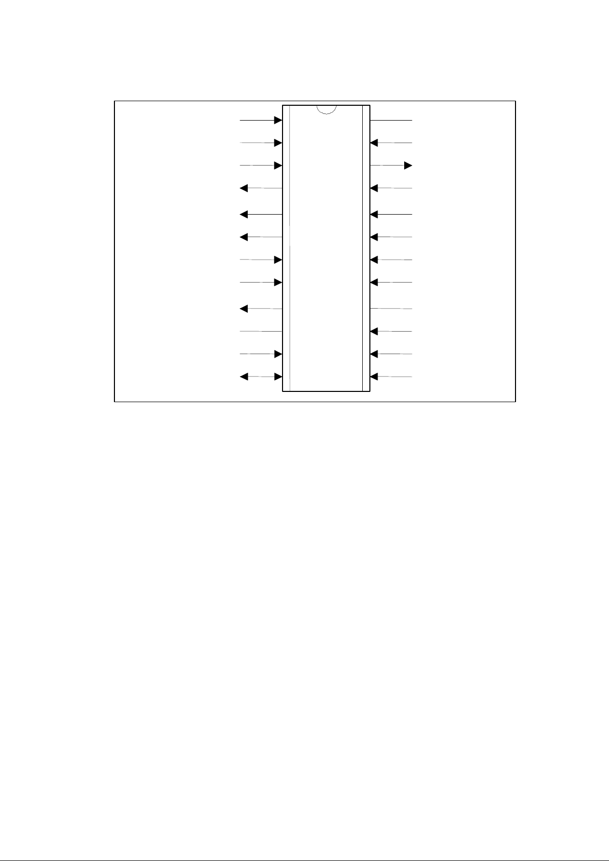
PIN CONFIGURATION
11
12
13
14
15
16
17
18
19
20
1
2
3
4
5
6
7
8
9
10
SDA
22
21
23
24
VCC
VT1/PII1
VREF
+12VIN
VCOREA
+3.3VIN
-12VIN
-5VIN/VT2/PII2
GNDA
VID1
FANIN1
VID4
BEEP/nGPO
FANIN3/PWMOUT1
nOVT
nSMI/PWMOUT2
GNDD
CLKIN
SCL
VID2
VID3
FANIN2
VID0

6
PIN DESCRIPTION
PIN
NAME
PIN
NO.
TYPE DESCRIPTION
VID4 1 IN
t
Voltage Supply readouts from Pentium IITM.
FANIN1 2 IN
ts
0V to 5V amplitude fan tachometer input.
FANIN2 3 IN
ts
0V to 5V amplitude fan tachometer input.
FANIN3 /
PWMOUT1
4 INts /
OUT
12t
0V to 5V amplitude fan tachometer input.
Fan speed control (PWM) output.
This multi-functional pin is programmable.
nOVT 5 OUT
12t
Over temperature Shutdown Output.
BEEP/nGP
O
6 OD
48
Beep (Default) / General purpose output
This multi-functional pin is programmable.
VID3 7 IN
t
Voltage Supply readouts from Pentium IITM.
CLKIN 8 IN
t
System clock input. Can select 48MHz or 24MHz or
14.318MHz. The default is 24MHz.
nSMI /
PWMOUT2
9 OD12 /
OUT
12t
System Management Interrupt (open drain). The default
state is disabled.
Fan speed control (PWM) output.
This multi-functional pin is programmable.
GNDD 10 DGROUND Internally connected to all digital circuitry.
SCL 11 IN
ts
Serial Bus Clock.
SDA 12 I/O
12ts
Serial Bus bi-directional Data.
VID2 13 IN
t
Voltage Supply readouts from Pentium IITM.
VID1 14 IN
t
Voltage Supply readouts from Pentium IITM.
VID0 15 IN
t
Voltage Supply readouts from Pentium IITM.
GNDA 16 AGROUND Internally connected to all analog circuitry. The ground
reference for all analog inputs.
-5VIN /
VT2 /
PII2
17 AIN 0V to 4.096V FSR Analog Inputs (Default).
Thermistor 2 terminal input.
Pentium II
TM
thermal 2 diode input.
This multi-functional pin is programmable.
-12VIN 18 AIN 0V to 4.096V FSR Analog Inputs.
+12VIN 19 AIN 0V to 4.096V FSR Analog Inputs.
+3.3VIN 20 AIN 0V to 4.096V FSR Analog Inputs.
VCOREA 21 AIN 0V to 4.096V FSR Analog Inputs.
VREF 22 AOUT Reference Voltage.
VT1 /
PII1
23 AIN Thermistor 1 terminal input. /
Pentium II
TM
thermal diode 1 input.
VCC (+5V) 24 POWER +5V VCC power. Bypass with the parallel combination of
10µF (electrolytic or tantalum) and 0.1µF (ceramic)
bypass capacitors.

7
PIN DESCRIPTION
I/O
12t
TTL level bi-directional pin with 12 mA source-sink capability
I/O
12ts
TTL level and schmitt trigger
OUT12 Output pin with 12 mA source-sink capability
AOUT Output pin(Analog)
OD12 Open-drain output pin with 12 mA sink capability
INt TTL level input pin
INts TTL level input pin and schmitt trigger
AIN Input pin(Analog)
8
FUNCTIONAL DESCRIPTION
GENERAL DESCRIPTION
The MON35W82 provides 6 analog positive
inputs, 3 fan speed monitor inputs, 2 PWM
(Pulse Width Modulation) output controls, 2 sets
for fan PWM (Pulse Width Modulation) control,
2 thermal inputs from remote thermistors or
2N3904 transistors or PenitumTM II (Deschutes)
thermal diode outputs, a beep function output
and a monitor function for the voltage,
temperature and fan counters. Once the
monitor function is initiated, the watchdog
monitors each function and stores the value. If
the monitored value is not within the limits
values, the interrupt status is set and an
interrupt can be generated.
Access Interface
The MON35W82 provides an I2C Serial Bus to
read/write internal registers. There are two
serial bus address registers, CR[48h] and
CR[4Ah] used to read/write all of the internal
registers. CR[48h] (default value 0101101) is
used to access all registers excluding the Bank
1 temperature sensor registers. CR[4Ah]
(default value 1001001)is used to access the
Bank 1 temperature sensor registers.
The serial bus access timings are shown in the
following figures.
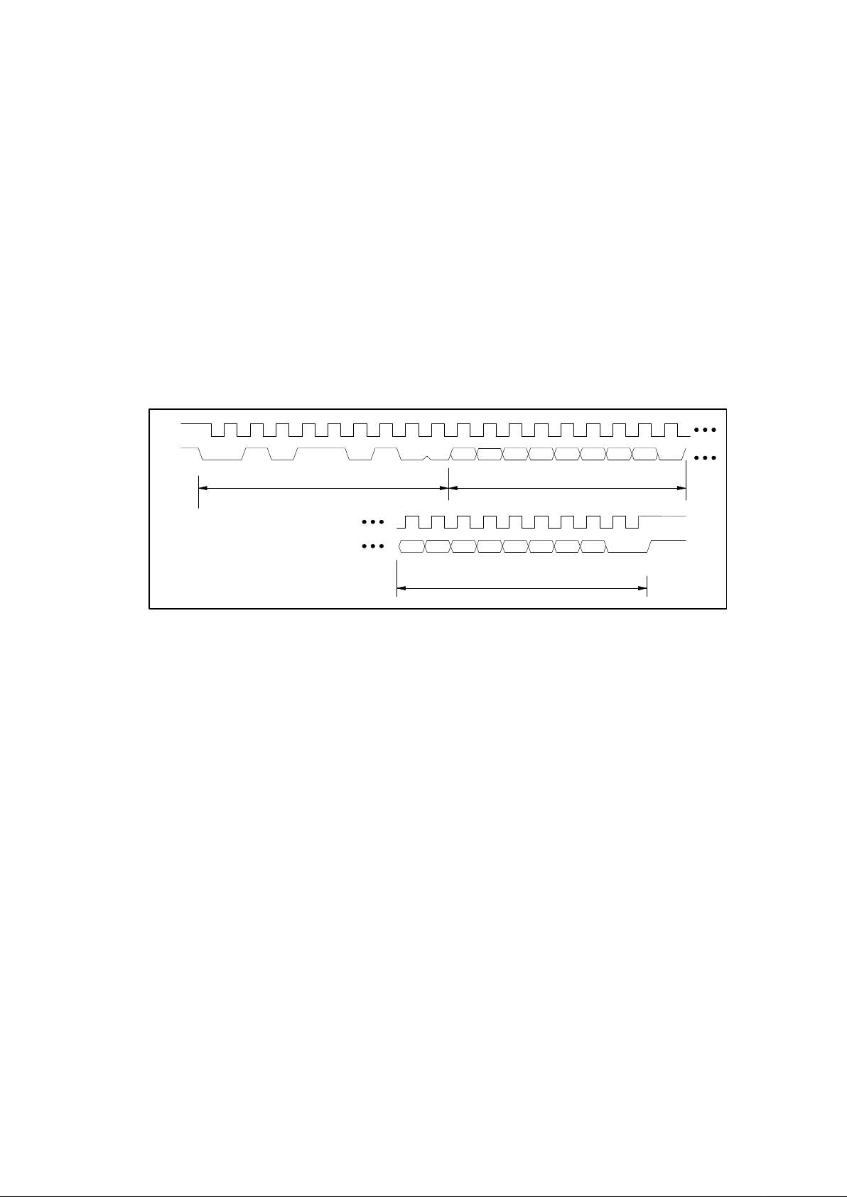
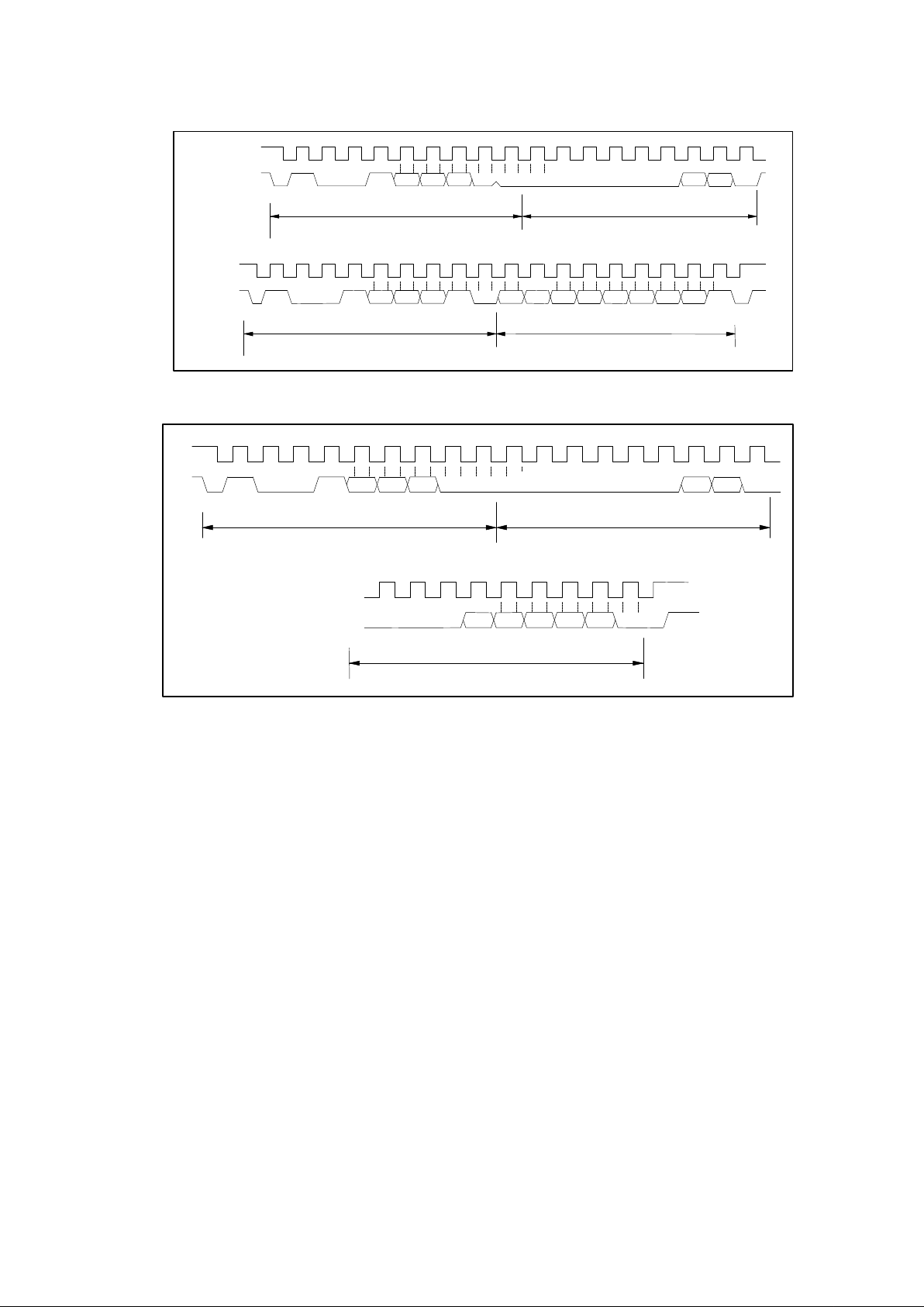
FIGURE 1 - SERIAL BUS WRITE TO INTERNAL ADDRESS REGISTER FOLLOWED BY
THE DATA BYTE
0
Start By
Master
0 1 0 1 1 0 1 D7 D6 D5 D4 D3 D2 D1 D0
Ack
by
MON35W42
R/nW
Ack
by
SCL
SDA
D7 D6 D5 D4 D3 D2 D1 D0
Ack
by
Stop
by
Master
SCL
SDA (Continued)
7 8 0 7 8
0
7 8
Frame 2
Internal Index Register Byte
(Continued)
Frame 3
Data Byte
Frame 1
Serial Bus Address Byte
MON35W42
MON35W42
9
FIGURE 2 - SERIAL BUS WRITE TO INTERNAL ADDRESS REGISTER ONLY
FIGURE 3 - SERIAL BUS READ FROM A REGISTER WITH THE INTERNAL ADDRESS
REGISTER PRESET TO DESIRED LOCATION
The serial bus timing of the temperature 2 and 3 is shown below:
FIGURE 4 - TYPICAL 2-BYTE READ FROM PRESET POINTER LOCATION (TEMP, TOS,
T
HYST
)
0
Start By
Master
0 1 0 1 1 0 1 D7 D6 D5 D4 D3 D2 D1 D0
Ack
by
R/nW
Ack
by
SCL
SDA
7 8 0 7 8
0
Frame 2
Internal Index Register Byte
Frame 1
Serial Bus Address Byte
Stop by
Master
MON35W42
MON35W42
0
Start By
Master
0 1 0 1 1 0 1 D7 D6 D5 D4 D3 D2 D1 D0
Ack
by
Master
R/nW
Ack
by
SCL
SDA
7 8 0 7 8
0
Frame 2
Internal Index Register Byte
Frame 1
Serial Bus Address Byte
Stop by
Master
MON35W42
0
Start By
Master
0 1 0 1 1 0 1 D7 D1 D0
Ack
by
Master
R/nW
Ack
by
SCL
SDA
7 8 0 7 8
Frame 2
MSB Data Byte
Frame 1
Serial Bus Address Byte
D7 D1 D0
0 7
Stop by
Master
...
... ...
Ack
by
Master
...
Frame 3
LSB Data Byte
MON35W42
10
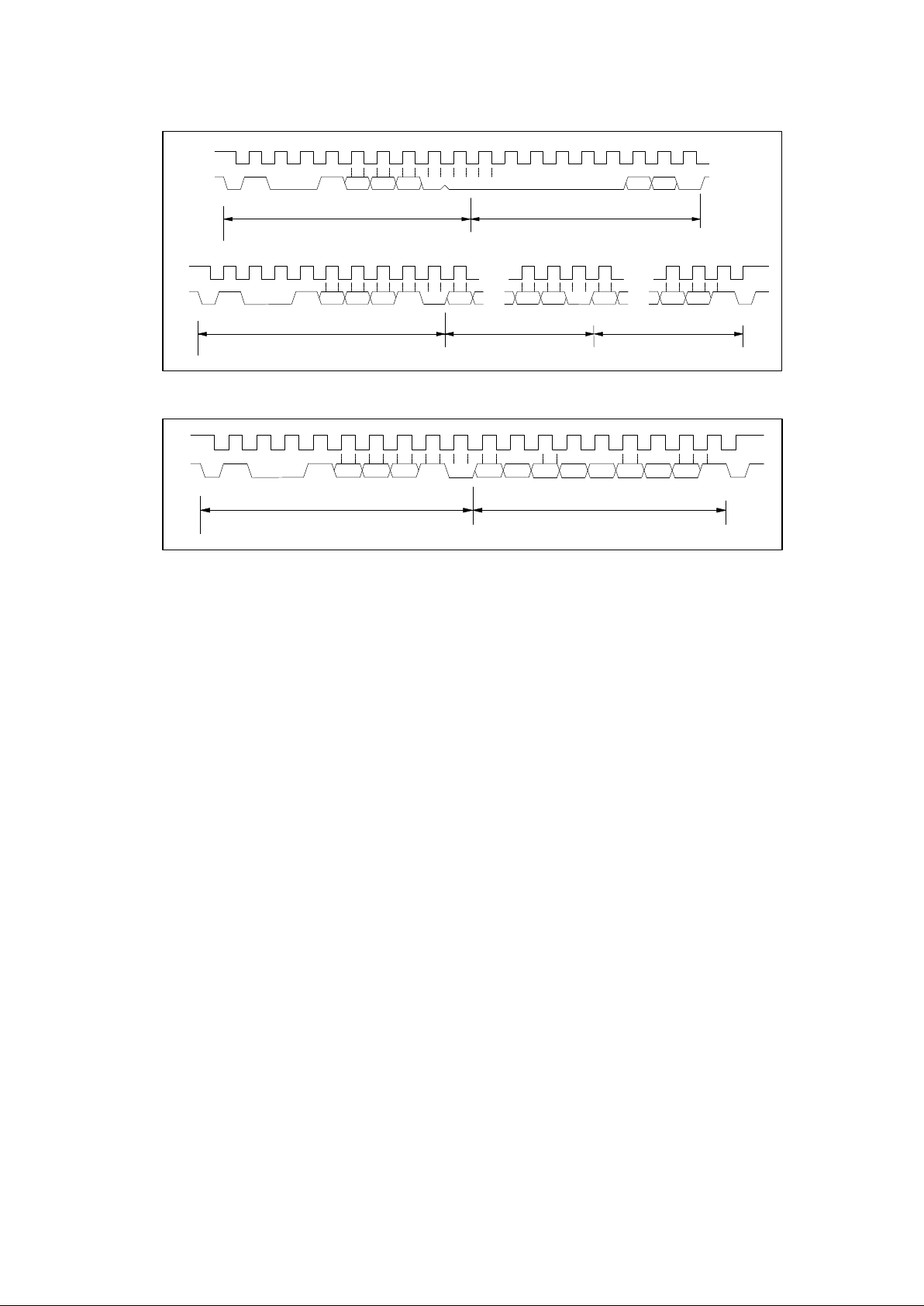
FIGURE 5 - TYPICAL POINTER SET FOLLOWED BY IMMEDIATE READ FOR 2-BYTE
REGISTER (TEMP, TOS, T
HYST
)
FIGURE 6 - TYPICAL READ 1-BYTE FROM CONFIGURATION REGISTER WITH
PRESET POINTER
0
Start By
Master
D7 D1 D0
Ack
by
Master
Ack
by
SCL
SDA
7 8 0 7 8
0
Frame 4
MSB Data Byte
Frame 3
Serial Bus Address Byte
D7 D1 D0
0 7
Stop by
Master
...
... ...
No Ack
by
Master
...
Frame 5
LSB Data Byte
0
Start By
Master
1 0 0 1 A2 A1 A0
R/nW
Ack
by
SCL
SDA
7 8 0
Frame 1
Serial Bus Address Byte
4
D1 D0
Ack
by
Frame 2
Pointer Byte
1 0 0 1 A2 A1 A0
R/nW
0 0 0 0 0 0
MON35W42
MON35W42
MON35W42
MON35W42
0
Start By
Master
D7 D2
Ack
by
SCL
SDA
7 8 0
Frame 2
Data Byte
Frame 1
Serial Bus Address Byte
D0
7
Stop by
Master
No Ack
by
Master
1 0 0 1 A2 A1 A0
R/nW
D1D5 D4 D3D6
8
11
FIGURE 7 - TYPICAL POINTER SET FOLLOWED BY IMMEDIATE READ FROM
CONFIGURATION REGISTER
FIGURE 8 - TEMPERATURE 2/3 CONFIGURATION REGISTER WRITE
0
Repea
Start
By Master
D7 D5 D4
Ack
by
SCL (Cont..)
SDA (Cont..)
7 8 0
Frame 4
MSB Data Byte
Frame 3
Serial Bus Address Byte
D2 D1 D0
7
Stop by
Master
No Ack
by
Master
0
Start By
Master
1 0 0 1 A2 A1 A0
R/nW
Ack
by
MON35W42
SCL
SDA
7 8 0
Frame 1
Serial Bus Address Byte
4
D1 D0
Ack
by
Frame 2
Pointer Byte
1 0 0 1 A2 A1 A0
R/nW
...
...
D6 D3
8
7 8
0 0 0 0 00
MON35W42
MON35W42
0
Ack
by
SCL (Cont...)
SDA (Cont...)
7 8
Frame 3
Configuration Data Byte
0 0 D4 D3 D2 D10 D0
Stop
by
Master
MON35W42
0
Start By
Master
1 0 0 1 A2 A1 A0
R/nW
Ack
by
MON35W42
SCL
SDA
7 8 0
Frame 1
Serial Bus Address Byte
4
D1 D0
Ack
by
Frame 2
Pointer Byte
0 0 0 0 0 0 0
7 8
MON35W42
12
FIGURE 9 - TEMPERATURE 2/3 TOS AND T
HYST
WRITE
ANALOG INPUTS
The analog inputs are normally used to monitor
the PC power supplies. The 8-bit ADC has a
16mv LSB and supports an input range of 0V to
4.096V. The CPU V-core, 3.3V and battery
voltage can be directly connected to these
analog inputs. Voltages higher than 4.096V
must be reduced to the specified input range.
An example using external resistors is shown in
Figure 10.
0
Ack
by
SCL (Cont...)
SDA (Cont...)
7 8
Frame 3
MSB Data Byte
0
Start By
Master
1 0 0 1 A2 A1 A0
R/nW
Ack
by
MON35W42
SCL
SDA
7 8 0
Frame 1
Serial Bus Address Byte
4
D1 D0
Ack
by
Frame 2
Pointer Byte
D6 D5 D4 D3 D2 D1D7 D0
0
7 8
D6 D5 D4 D3 D2 D1D7 D0
Ack
by
Stop
by
Master
Frame 4
LSB Data Byte
7 8
0
0
0 0 0 0
MON35W42
MON35W42
MON35W42
13
FIGURE 10
Monitor over 4.096V voltage:
The input voltage +12VIN can be expressed as following equation.
12
1
2
1 2
VIN V
R
R R
= ×
+
The value of R1 and R2 can be selected as 28K
Ohms and 10K Ohms, respectively, when the
input voltage V1 is 12V. The node voltage of
+12VIN must be less than 4.096V for the
maximum input range of the 8-bit ADC. The Vcc
Pin (Pin 24) is connected to the power supply
VCC (+5V). There are two functions in this pin.
The first function is to supply internal analog
power in the MON35W82 and the second
function is to monitor this voltage. The Vcc Pin
is connected to internal serial resistors to
monitor the +5V voltage. The value of two serial
resistors are 34K ohms and 50K ohms so that
the input voltage to the ADC is 2.98V which is
less than 4.096V of ADC maximum input
voltage. The voltage equation can be
represented as follows.
VCORE
Pin 21
+3.3VIN
12VIN
Pin 20
Pin 19
Pin 24
Vcc (+5V)
N12VIN Pin 18
R6
R1
V1
N5VIN
Positive Input
Negative Input
8-bit ADC
with
16mV LSB
Typical Thermister Connection
10K, 1%
R
THM
VREF Pin 22
VT1 Pin 23
Pin 17
Positive Inputs
R5
R7
R8
10K, 25 C
**The connections of VT2
is same as VT1
R2
R
V3
V4

14
V VCC
K
K K
V
in
= ×
+
≅
50
50 34
2 98
Ω
Ω Ω
.
where VCC is set to 5V.
Monitor negative voltage:
The negative voltage should be connected to
two series resistors and a positive voltage VREF
(equal to 3.6V). In Figure 10, voltages V3 and
V4 are two negative voltages, -12V and -5V
respectively. The voltage V3 is connected to two
series resistors and then is connected to VREF
which is a positive voltage. The voltage on node
N12VIN must be between 0V and 4.096V. If
R5=232K ohms and R6=56K ohms, the input
voltage of node N12VIN can be calculated as
follows:
where VREF is equal 3.6V.
If the V3 is equal to -12V then the voltage is
equal to 0.567V and the converted hexadecimal
data is set to 35h by the 8-bit ADC with 16mV-
LSB.This monitored value should be converted
to the real negative voltage and the express
equation is shown as follows.
Where β is 232K/(232K+56K). If the N2VIN is 0.567 then the V3 is approximately equal to -12V.
The another negative voltage input V6
(approximate -5V) can also be evaluated by a
similar method and the serial resistors can be
selected with R7=120K ohms and R8=56K
ohms. The expression equation of V6 With -5V
voltage is shown as follows.
V
N VIN VREF
6
5
1
=
−
×−γ
γ
Where the ϒ is set to 120K/(120K+56K). If the
monitored ADC value in the N5VIN channel is
0.8635, VREF=3.6V and the parameter ϒ is
0.6818 then the negative voltage of V6 can be
evaluated to be -5V.
N VIN VREF V V12
3 3
= + × +
( ) ( )
K232
Ω
KK232
56
+ΩΩ
V
N VIN VREF
3
12
1
=
− ×−β
β
15
Monitor temperature from thermistor:
The MON35W82 can connect to three
thermistors to measure three different
environmental temperatures. The specification
of the thermistors are (1) β value is 3435K, (2)
resistor value is 10K ohms at 25°C. In Figure
10, the thermistor R
THM
is connected to VT1 and
VT1 is connected through a 10K ohm series
resistor to VREF.
Monitor temperature from Pentium II
TM
thermal diode or bipolar transistor 2N3904
The MON35W82 can interface to the Pentium
II™ (Deschutes) thermal diode interface or a
2N3904 transistor. The circuit connection is
shown in Figure 11. The Pentium II™ D- pin is
connected to ground (GND) and the D+ pin is
connected to the PII1 or PII2 pin of the
MON35W82. A 30K-ohm resistor must be
connected from the PIIx pin to the VREF pin to
supply the diode bias current and a bypass
capacitor C=3300pF must be added to filter the
high frequency noise. If a 2N3904 transistor is
used, the Base (B) and Collector (C) must be
tied together to act as a thermal diode.
FIGURE 11
2N3904
C
E
B
R=30K, 1%
C=3300pF
Bipolar Transistor
Temperature Sensor
Pentium II
CPU D+
D-
Therminal
Diode
C=3300pF
R=30K, 1%
VREF
PIITDx
PIITDx
OR
MON35W82
 Loading...