

SMSC LPC47U337, LPC47U332 Datasheet

LPC47U33x
100 Pin Enhanced Super I/O for LPC Bus with
Consumer Features and SMBus Controller
FEATURES
• 3.3 Volt Operation (5V Tolerant)
• LPC Interface
• Floppy Disk Controller (Supports 2 FDCs)
• Multi-Mode Parallel Port
• One Full Function UART
• MPU-401 MIDI UART
• 8042 Keyboard Controller
• Dual Game Port
• SMBus Controller
• Programmable Wakeup Event Interface
(nIO_PME Pin)
• SMI Support (nIO_SMI Pin)
• GPIO Pins (37)
• Fan Speed Control Output
• Fan Tachometer Input
• ISA IRQ to Serial IRQ Conversion
• XNOR Chain
• PC99 and ACPI 1.0 Compliant
• ISA Plug-and-Play Compatible Register Set
• Intelligent Auto Power Management
• 2.88MB Super I/O Floppy Disk Controller
- Licensed CMOS 765B Floppy Disk
Controller
- Software and Register Compatible with
SMSC's Proprietary 82077AA
Compatible Core
- Configurable Open Drain/Push-Pull
Output Drivers
- Supports Vertical Recording Format
- 16-Byte Data FIFO
- 100% IBM® Compatibility
- Detects All Overrun and Underrun
Conditions
- Sophisticated Power Control Circuitry
(PCC) Including Multiple Powerdown
Modes for Reduced Power
Consumption
- DMA Enable Logic
- Data Rate and Drive Control Registers
- 480 Address, up to 15 IRQ and 3 DMA
Options
• Enhanced Digital Data Separator
- 2 Mbps, 1 Mbps, 500 Kbps, 300 Kbps,
250 Kbps Data Rates
- Programmable Precompensation
Modes
• Keyboard Controller
- 8042 Software Compatible
- 8-Bit Microcomputer
- 2k Bytes of Program ROM
- 256 Bytes of Data RAM
- Four Open Drain Outputs Dedicated for
Keyboard/Mouse Interface
- Asynchronous Access to Two Data
Registers and One Status Register
- Supports Interrupt and Polling Access
- 8-Bit Counter Timer
- Port 92 Support
- Fast Gate A20 and KRESET Outputs
• Serial Port
- One Full Function Serial Port
- High Speed NS16C550 Compatible
UART with Send/Receive 16-Byte
FIFOs
- Supports 230k and 460k Baud
- Programmable Baud Rate Generator
- Modem Control Circuitry
- 480 Address and 15 IRQ Options
- Second UART for MPU-401 MIDI
Interface

2
• Multi-Mode Parallel Port with ChiProtect™
- Standard Mode IBM PC/XT®, PC/AT®,
and PS/2™ Compatible Bidirectional
Parallel Port
- Enhanced Parallel Port (EPP)
Compatible - EPP 1.7 and EPP 1.9
(IEEE 1284 Compliant)
- IEEE 1284 Compliant Enhanced
Capabilities Port (ECP)
- ChiProtect Circuitry for Protection
Against Damage Due to Printer PowerOn
- 480 Address, up to 15 IRQ and 3 DMA
Options
• Pin Reduced ISA Host Interface (LPC Bus)
- Multiplexed Command, Address and
Data Bus
- 8-Bit I/O Transfers
- 8-Bit DMA Transfers
- 16-Bit Address Qualification
- Serial IRQ Interface Compatible with
Serialized IRQ Support for PCI
Systems
- Power Management Event (nIO_PME)
Interface Pin
• 100 Pin QFP Package
GENERAL DESCRIPTION
The LPC47U33x* is a 3.3V PC99 compliant
Enhanced Super I/O controller. The LPC47U33x
implements the LPC interface, a pin reduced
ISA interface which provides the same or better
performance as the ISA/X-bus with a substantial
savings in pins used. The part provides 37
GPIO pins, a dual game port interface, MPU401 MIDI support and ISA IRQ to serial IRQ
conversion. The part also provides a fan speed
control output and a fan tachometer input.
The LPC47U33x incorporates a keyboard
interface, SMSC's true CMOS 765B floppy disk
controller, advanced digital data separator, one
16C550A compatible UART, one MPU-401 MIDI
UART, one Multi-Mode parallel port which
includes ChiProtect circuitry plus EPP and ECP,
and Intelligent Power Management including
ACPI, SMI and PME support. The true CMOS
765B core provides 100% compatibility with IBM
PC/XT and PC/AT architectures in addition to
providing data overflow and underflow
protection. The SMSC advanced digital data
separator incorporates SMSC's patented data
separator technology, allowing for ease of
testing and use. The on-chip UART is
compatible with the NS16C550A. The parallel
port is compatible with IBM PC/AT architecture,
as well as IEEE 1284 EPP and ECP. The
LPC47U33x incorporates sophisticated power
control circuitry (PCC). The PCC supports
multiple low power modes. The LPC47U33x
also incorporates SMBus Controller.
The LPC47U33x supports the ISA Plug-andPlay Standard (Version 1.0a) and provides the
recommended functionality to support Windows
'95 and PC99. The I/O Address, DMA Channel
and Hardware IRQ of each logical device in the
LPC47U33x may be reprogrammed through the
internal configuration registers. There are 480
I/O address location options, a Serialized IRQ
interface, and three DMA channels. The
LPC47U33x does not require any external filter
components and is therefore easy to use and
offers lower system costs and reduced board
area. The LPC47U33x is software and register
compatible with SMSC's proprietary 82077AA
core.
IBM, PC/XT and PC/AT are registered trademarks and PS/2 is a
trademark of International Business Machines Corporation
SMSC is a registered trademark and Ultra I/O, ChiProtect, and MultiMode are trademarks of Standard Microsystems Corporation
*The “x” in the part number is a designator that changes depending upon the particular BIOS used
inside the specific chip. “2” denotes AMI Keyboard BIOS and “7” denotes Phoenix 42i Keyboard
BIOS.

3
TABLE OF CONTENTS
FEATURES....................................................................................................................................... 1
GENERAL DESCRIPTION ................................................................................................................ 2
PIN CONFIGURATION...................................................................................................................... 6
DESCRIPTION OF PIN FUNCTIONS ................................................................................................ 7
Buffer Type Descriptions..............................................................................................................12
Pins That Require External Pullup Resistors................................................................................. 13
BLOCK DIAGRAM.......................................................................................................................... 14
3.3 VOLT OPERATION / 5 VOLT TOLERANCE.............................................................................. 15
POWER FUNCTIONALITY.............................................................................................................. 15
VCC Power .................................................................................................................................. 15
VTR Support................................................................................................................................ 15
VREF PIN .................................................................................................................................... 15
Internal PWRGOOD.................................................................................................................... 15
Indication of 32kHz Clock............................................................................................................. 16
Trickle Power Functionality.......................................................................................................... 16
Maximum Current Values............................................................................................................. 17
Power Management Events (PME/SCI)........................................................................................ 17
FUNCTIONAL DESCRIPTION......................................................................................................... 18
Super I/O Registers ..................................................................................................................... 18
Host Processor Interface (LPC).................................................................................................... 18
LPC Interface............................................................................................................................... 19
FLOPPY DISK CONTROLLER........................................................................................................ 23
FDC Internal Registers................................................................................................................. 23
Status Register Encoding............................................................................................................. 36
DMA Transfers............................................................................................................................. 40
Controller Phases........................................................................................................................ 40
Command Set/Descriptions ......................................................................................................... 42
Instruction Set ............................................................................................................................. 46
Data Transfer Commands............................................................................................................ 58
Control Commands...................................................................................................................... 64
Direct Support for Two Floppy Drives...........................................................................................71
SERIAL PORT (UART).................................................................................................................... 72
Register Description..................................................................................................................... 72
Programmable Baud Rate Generator (AND Divisor Latches DLH, DLL)........................................79
Effect Of The Reset on Register File ............................................................................................ 80
FIFO Interrupt Mode Operation.................................................................................................... 80
FIFO Polled Mode Operation........................................................................................................ 80
Notes On Serial Port Operation.................................................................................................... 85
MPU-401 MIDI UART...................................................................................................................... 86
OVERVIEW.................................................................................................................................86
HOST INTERFACE...................................................................................................................... 87
MPU-401 COMMAND CONTROLLER.......................................................................................... 90
MIDI UART.................................................................................................................................. 91
MPU-401 CONFIGURATION REGISTERS .................................................................................. 92
PARALLEL PORT........................................................................................................................... 93
IBM XT/AT Compatible, Bi-Directional and EPP Modes................................................................94
EPP 1.9 Operation ....................................................................................................................... 96

4
EPP 1.7 Operation ....................................................................................................................... 97
Extended Capabilities Parallel Port............................................................................................... 99
Vocabulary .................................................................................................................................100
ECP Implementation Standard ....................................................................................................101
PARALLEL PORT FLOPPY DISK CONTROLLER.........................................................................112
FDC on Parallel Port Pin.............................................................................................................113
POWER MANAGEMENT ...............................................................................................................114
FDC Power Management............................................................................................................114
DSR From Powerdown ...............................................................................................................114
Wake Up From Auto Powerdown................................................................................................114
Register Behavior .......................................................................................................................114
Pin Behavior...............................................................................................................................115
UART Power Management..........................................................................................................117
Parallel Port................................................................................................................................117
MPU-401 Power Management.....................................................................................................117
SERIAL IRQ...................................................................................................................................118
ISA IRQ TO SERIAL IRQ CONVERSION CAPABILITY ...............................................................122
8042 KEYBOARD CONTROLLER DESCRIPTION.........................................................................123
Keyboard Interface......................................................................................................................124
External Keyboard and Mouse Interface......................................................................................125
Keyboard Power Management ....................................................................................................125
Interrupts....................................................................................................................................126
Memory Configurations ...............................................................................................................126
Register Definitions.....................................................................................................................126
External Clock Signal ..................................................................................................................127
Default Reset Conditions.............................................................................................................127
Latches On Keyboard and Mouse IRQs.......................................................................................130
Keyboard and Mouse Wake-up...................................................................................................131
GENERAL PURPOSE I/O ..............................................................................................................133
GPIO Pins..................................................................................................................................133
Description .................................................................................................................................134
GPIO Control..............................................................................................................................135
GPIO Operation..........................................................................................................................137
GPIO PME and SMI Functionality...............................................................................................138
Either Edge Triggered Interrupts .................................................................................................140
LED Functionality .......................................................................................................................140
Watch Dog Timer .......................................................................................................................140
SYSTEM MANAGEMENT INTERRUPT (SMI)................................................................................142
SMI Registers.............................................................................................................................142
ACPI Support Register for SMI Generation..................................................................................143
PME SUPPORT .............................................................................................................................144
WAKE ON SPECIFIC KEY OPTION...........................................................................................146
FAN SPEED CONTROL AND MONITORING.................................................................................147
Fan Speed Control ......................................................................................................................147
Fan Tachometer Input.................................................................................................................148
SECURITY FEATURE....................................................................................................................153
GPIO Device Disable Register Control........................................................................................153
Device Disable Register..............................................................................................................153
GAME PORT LOGIC .....................................................................................................................154

5
SMBUS CONTROLLER.................................................................................................................157
Overview ....................................................................................................................................157
Configuration Registers...............................................................................................................157
Runtime Registers......................................................................................................................157
Pin Multiplexing ..........................................................................................................................164
SMBus Timeouts ........................................................................................................................164
SMBus Timeout..........................................................................................................................165
RUNTIME REGISTERS..................................................................................................................166
Runtime Registers Block Summary .............................................................................................166
Runtime Registers Block Description...........................................................................................169
CONFIGURATION .........................................................................................................................201
OPERATIONAL DESCRIPTION.....................................................................................................223
Maximum Guaranteed Ratings....................................................................................................223
Normal Operation.......................................................................................................................223
DC ELECTRICAL CHARACTERISTICS ......................................................................................223
TIMING DIAGRAMS ......................................................................................................................227
ECP Parallel Port Timing............................................................................................................238
PACKAGE OUTLINE .....................................................................................................................248
Board Test Mode ........................................................................................................................249
80 Arkay Drive
Hauppauge, NY 11788
(516) 435-6000
FAX (516) 273-3123
6
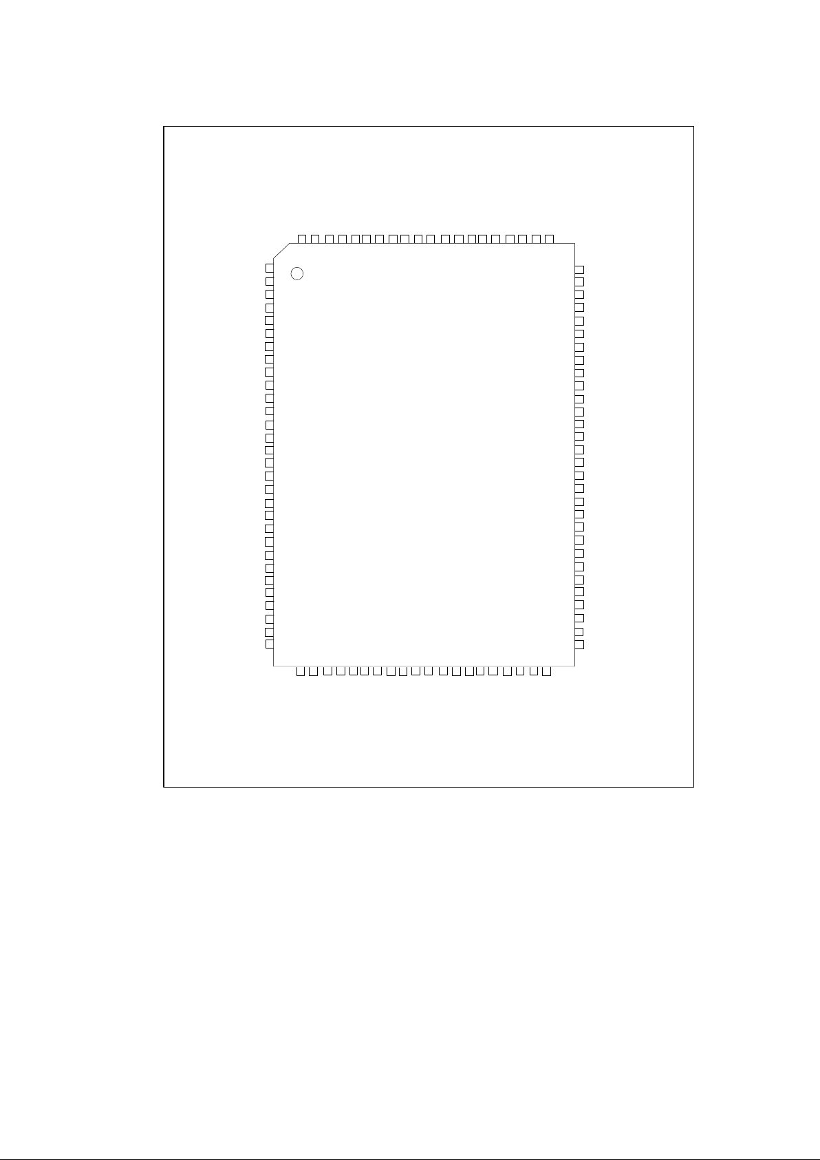
PIN CONFIGURATION
LPC47U33x
100 PIN QFP
GP40/DRVDEN0
GP41/DRVDEN1
nMTR0
nDSKCHG
nDS0
CLKI32
VSS
nDIR
nSTEP
nWDATA
nWGATE
nHDSEL
nINDEX
nTRK0
nWRTPRT
nRDATA
GP42/nIO_PME
VTR
CLOCKI
LAD0
LAD1
LAD2
LAD3
nLFRAME
nLDRQ
nPCI_RESET
nLPCPD
GP43/DDRC/FDC_PP
PCI_CLK
SER_IRQ
1
2
3
4
5
6
7
8
9
10
11
12
13
14
15
16
17
18
19
20
21
22
23
24
25
26
27
28
29
30
nACK
BUSY
PE
SLCT
VSS
PD7
PD6
PD5
PD4
PD3
PD2
PD1
PD0
nSLCTIN
nINIT
VCC
GP37/nA20M
GP36/nKBDRST
GP35/IRQ14
GP34/IRQ12
VSS
MCLK
MDAT
KCLK
KDAT
GP33/FAN
GP32/SDAT
VCC
GP31/FAN_TACH
GP30/SCLK
80
79
78
77
76
75
74
73
72
71
70
69
68
67
66
65
64
63
62
61
60
59
58
57
56
55
54
53
52
51
VSS
GP10/J1B1
GP11/J1B2
GP12/J2B1
GP13/J2B2
GP14/J1X
GP15/J1Y
GP16/J2X
GP17/J2Y
AVSS
GP20/P17/nDS1
GP21/P16/IRQ6
GP22/P12/nMTR1
VREF
GP24/SYSOPT
GP25/MIDI_IN
GP26/MIDI_OUT
GP60/LED1
GP61/LED2
GP27/nIO_SMI
31323334353637383940414243444546474849
50
GP57/IRQ15
GP56/IRQ11
GP55/IRQ10
GP54/IRQ9
GP53/IRQ7
GP52/IRQ5
GP51/IRQ4
VCC
GP50/IRQ3
nDCD
nRI
nDTR
nCTS
nRTS
nDSR
TXD
RXD
nSTROBE
nALF
nERROR
100
99
98
97
96
95
94
93
92
91
90
89
88
87
86
85
84
83
82
81
7
DESCRIPTION OF PIN FUNCTIONS
The pins that have multiple functions are named
with the primary function first. The primary
function is the function of the pin at default. For
example, GP40/DRVDEN0 pin has the primary
function of GP40.
TABLE 1 - PIN FUNCTION DESCRIPTION
QFP
PIN #
NAME FUNCTION
BUFFER
TYPE
BUFFER MODE PER
FUNCTION (NOTE 1)
FDD INTERFACE
1
GP40/DRVDEN0 General Purpose I/O/Drive
Density Select 0
IO12 IO12/(O12/OD12)
2
GP41/DRVDEN1 General Purpose I/O/Drive
Density Select 1
IO12 IO12/(O12/OD12)
3
nMTR0 Motor On 0 O12 (O12/OD12)
5
nDS0 Drive Select 0 O12 (O12/OD12)
8
nDIR Step Direction O12 (O12/OD12)
9
nSTEP Step Pulse O12 (O12/OD12)
10
nWDATA Write Disk Data O12 (O12/OD12)
11
nWGATE Write Gate O12 (O12/OD12)
12
nHDSEL Head Select O12 (O12/OD12)
13
nINDEX Index Pulse Input IS IS
14
nTRK0 Track 0 IS IS
15
nWRTPRT Write Protected IS IS
16
nRDATA Read Disk Data IS IS
4
nDSKCHG Disk Change IS IS
LPC INTERFACE
20
LAD0 Multiplexed Command
Address and Data 0
PCI_IO PCI_IO
21
LAD1 Multiplexed Command
Address and Data 1
PCI_IO PCI_IO
22
LAD2 Multiplexed Command
Address and Data 2
PCI_IO PCI_IO
23
LAD3 Multiplexed Command
Address and Data 3
PCI_IO PCI_IO
24
nLFRAME Frame PCI_I PCI_I
25
nLDRQ Encoded DMA Request PCI_O PCI_O
26
nPCI_RESET PCI Reset PCI_I PCI_I
27
nLPCPD Power Down (Note 2) PCI_I PCI_I
29
PCI_CLK PCI Clock PCI_ICLK PCI_ICLK
30
SER_IRQ Serial IRQ PCI_IO PCI_IO
8
QFP
PIN #
NAME FUNCTION
BUFFER
TYPE
BUFFER MODE PER
FUNCTION (NOTE 1)
GAME PORT INTERFACE
32
GP10/J1B1 General Purpose I/O/
Joystick 1 Button 1
IS/O8 (IS/O8/OD8)/IS
33
GP11/J1B2 General Purpose I/O/
Joystick 1 Button 2
IS/O8 (IS/O8/OD8)/IS
34
GP12/J2B1 General Purpose I/O/
Joystick 2 Button 1
IS/O8 (IS/O8/OD8)/IS
35
GP13/J2B2 General Purpose I/O/
Joystick 2 Button 2
IS/O8 (IS/O8/OD8)/IS
36
GP14/J1X General Purpose I/O/
Joystick 1 X-Axis
IO12 (I/O12/OD12)/IO12
37
GP15/J1Y General Purpose I/O/
Joystick 1 Y-Axis
IO12 (I/O12/OD12)/IO12
38
GP16/J2X General Purpose I/O/
Joystick 2 X-Axis
IO12 (I/O12/OD12)/IO12
39
GP17/J2Y General Purpose I/O/
Joystick 2 Y-Axis
IO12 (I/O12/OD12)/IO12
MPU-401 INTERFACE
46
GP25/MIDI_IN General Purpose I/O/
MIDI_IN
IO8 (I/O8/OD8)/I
47
GP26/MIDI_OUT General Purpose I/O/
MIDI_OUT
IO12 (I/O12/OD12)/O12
SMBus INTERFACE
51
GP30/SCLK General Purpose I/O/SMBus
Clock
IO12 (I/O12/OD12)/IO12
54
GP32/SDAT General Purpose I/O/SMBus
Data
IO12 (I/O12/OD12)/IO12
General Purpose I/O Pins
48
GP60/LED1 General Purpose I/O/ LED1
(Note 8)
IO12 (I/O12/OD12)/O12
49
GP61/LED2 General Purpose I/O/ LED2
(Note 8)
IO12 (I/O12/OD12)/O12
41
GP20/P17/nDS1 General Purpose I/O/ P17/
Dive Select 1
IO12 (I/O12/OD12)/IO12/
IO12
43
GP22/P12/nMTR1 General Purpose I/O/ P12/
Motor On 1
IO12 (I/O12/OD12)/IO12/
IO12
45
GP24/SYSOPT General Purpose I/O/
System Option (Note 6)
IO8 (I/O8/OD8)
50
GP27/nIO_SMI General Purpose I/O/System
Management Interrupt
IO12 (I/O12/OD12)/ OD12
9
QFP
PIN #
NAME FUNCTION
BUFFER
TYPE
BUFFER MODE PER
FUNCTION (NOTE 1)
17
GP42/nIO_PME General Purpose I/O/ Power
Management Event
IO12 (I/O12/OD12)/ OD12
28
GP43/DDRC/
FDC_PP
General Purpose I/O/ Device
Disable Reg. Control/ FDC
on Parallel Port
IO8 (I/O8/OD8)/I/I
92
GP50/IRQ3 General Purpose I/O/ IRQ3 IO8 (I/O8/OD8)/I
94
GP51/IRQ4 General Purpose I/O/ IRQ4 IO8 (I/O8/OD8)/I
95
GP52/IRQ5 General Purpose I/O/ IRQ5 IO8 (I/O8/OD8)/I
42
GP21/P16/IRQ6 General Purpose I/O/ P16/
IRQ6
IO8 (I/O8/OD8)/IO8/I
96
GP53/IRQ7 General Purpose I/O/ IRQ7 IO12 (I/O12/OD12)/I
97
GP54/IRQ9 General Purpose I/O/ IRQ9 IO8 (I/O8/OD8)/I
98
GP55/IRQ10 General Purpose I/O/ IRQ10 IO8 (I/O8/OD8)/I
99
GP56/IRQ11 General Purpose I/O/ IRQ11 IO8 (I/O8/OD8)/I
61
GP34/IRQ12 General Purpose I/O/IRQ12 IO8 (I/O8/OD8)/I
62
GP35/IRQ14 General Purpose I/O/IRQ14 IO8 (I/O8/OD8)/I
100
GP57/IRQ15 General Purpose I/O/ IRQ15 IO8 (I/O8/OD8)/I
FAN CONTROL PINS
52
GP31/FAN_TACH General Purpose I/O/Fan
Tachometer Input
IO12 (I/O12/OD12)/I
55
GP33/FAN General Purpose I/O/Fan
Control (Note 4)
IO12 (I/O12/OD12)/
(O12/OD12)
KEYBOARD/MOUSE INTERFACE
56
KDAT Keyboard Data IOD16 IOD16
57
KCLK Keyboard Clock IOD16 IOD16
58
MDAT Mouse Data IOD16 IOD16
59
MCLK Mouse Clock IOD16 IOD16
63
GP36/nKBDRST General Purpose
I/O/Keyboard Reset
(Note 7)
IO8 (I/O8/OD8)/O8
64
GP37/nA20M General Purpose I/O/Gate
A20 (Note 7)
IO8 (I/O8/OD8)/O8
PARALLEL PORT INTERFACE
66
nINIT/nDIR Initiate Output/FDC Direction
Control
(OD14/
OP14)/OD14
(OD14/OP14)/OD14
67
nSLCTIN/nSTEP Printer Select Input/FDC
Step Pulse
(OD14/
OP14)/OD14
(OD14/OP14)/OD14
68
PD0/nINDEX Port Data 0/FDC Index IOP14/IS IOP14/IS
69
PD1/nTRK0 Port Data 1/FDC Track 0 IOP14/IS IOP14/IS
10
QFP
PIN #
NAME FUNCTION
BUFFER
TYPE
BUFFER MODE PER
FUNCTION (NOTE 1)
70
PD2/nWRTPRT Port Data 2/FDC Write
Protected
IOP14/IS IOP14/IS
71
PD3/nRDATA Port Data 3/FDC Read Disk
Data
IOP14/IS IOP14/IS
72
PD4/nDSKCHG Port Data 4/FDC Disk
Change
IOP14/IS IOP14/IS
73
PD5 Port Data 5 IOP14 IOP14
74
PD6/nMTR0 Port Data 6/FDC Motor On 0 IOP14/OD14 IOP14/OD14
75
PD7 Port Data 7 IOP14 IOP14
77
SLCT/nWGATE Printer Selected Status/FDC
Write Gate
I/OD12 I/OD12
78
PE/nWDATA Paper End/FDC Write Data I/OD12 I/OD12
79
BUSY/nMTR1 Busy/FDC Motor On I/OD12 I/OD12
80
nACK/nDS1 Acknowledge/FDC Drive
Select 1
I/OD12 I/OD12
81
nERROR/nHDSEL Error/FDC Head Select I/OD12 I/OD12
82
nALF/nDRVDEN0 Autofeed Output/FDC
Density Select
(OD14/OP14)
/OD14
(OD14/OP14)/OD14
83
nSTROBE/nDS0 Strobe Output/FDC Drive
Select
(OD14/OP14)
/OD14
(OD14/OP14)/OD14
SERIAL PORT INTERFACE
84
RXD Receive Data IS IS
85
TXD Transmit Data O12 O12
86
nDSR Data Set Ready I I
87
nRTS Request to Send O8 O8
88
nCTS Clear to Send I I
89
nDTR Data Terminal Ready O6 O6
90
nRI Ring Indicator I I
91
nDCD Data Carrier Detect I I
POWER PINS
53,
65,
93
VCC +3.3 Volt Supply Voltage
18
VTR +3.3 Volt Standby Supply
Voltage (Note 5)
7, 31,
60,
76
VSS Ground
40
AVSS Analog Ground

11
QFP
PIN #
NAME FUNCTION
BUFFER
TYPE
BUFFER MODE PER
FUNCTION (NOTE 1)
44
VREF Reference Voltage (5V or
3.3V)
CLOCK PINS
6
CLKI32 32.768kHz Standby Clock
Input (Note 3)
IS IS
19
CLOCKI 14.318MHz Clock Input IS IS
Note: There are no internal pullups on any of the pins in the LPC47U33x.
Note: The "n" as the first letter of a signal name indicates an "Active Low" signal.
Note 1: Buffer Modes per function on multiplexed pins are separated by a slash “/”. Buffer Modes in
parenthesis represent multiple buffer modes for a single pin function.
Note 2: The nLPCPD pin may be tied high. The LPC interface will function properly if the
nPCI_RESET signal follows the protocol defined for the nLRESET signal in the “Low Pin
Count Interface Specification”.
Note 3: If the 32kHz input clock is not used the CLKI32 pin must be grounded. There is a bit in the
configuration register at 0xF0 in Logical Device A that indicates whether or not the 32KHz
clock is connected. This bit determines the clock source for the fan tachometer, LED and
“wake on specific key” logic.
Note 4: The fan control pin FAN comes up as an output and low following a VCC POR and Hard
Reset. This pin powers up as an input on VTR POR and may not be used for wakeup events
under VTR power (VCC=0).
Note 5: VTR can be connected to VCC if no wakeup functionality is required.
Note 6: The GP24/SYSOPT pin requires an external pulldown resistor to put the base IO address for
configuration at 0x02E. An external pullup resistor is required to move the base IO address
for configuration to 0x04E.
Note 7: External pullups must be placed on the nKBDRST and nA20M pins. These pins are GPIOs
that are inputs after an initial power-up (VTR POR). If the nKBDRST and nA20M functions
are to be used, the system must ensure that these pins are high.
Note 8: The LED pins are powered by VTR so that the LEDs can be controlled when the part is under
VTR power.

12
Buffer Type Descriptions
IO12 Input/Output, 12mA sink, 6mA source.
IS/O12 Input with Schmitt Trigger/Output, 12mA sink, 6mA source.
O12 Output, 12mA sink, 6mA source.
OD12 Open Drain Output, 12mA sink.
O6 Output, 6mA sink, 3mA source.
O8 Output, 8mA sink, 4mA source.
OD8 Open Drain Output, 8mA sink
IO8 Input/Output, 8mA sink, 4mA source.
IS/O8 Input with Schmitt Trigger/Output, 8mA sink, 4mA source.
OD14 Open Drain Output, 14mA sink.
OP14 Output, 14mA sink, 14mA source.
IOP14 Input/Output, 14mA sink, 14mA source. Backdrive protected.
IOD16 Input/Output (Open Drain), 16mA sink.
O4 Output, 4mA sink, 2mA source.
I Input TTL Compatible.
IS Input with Schmitt Trigger.
PCI_IO Input/Output. These pins meet the PCI 3.3V AC and DC Characteristics. (Note 1)
PCI_O Output. These pins meet the PCI 3.3V AC and DC Characteristics. (Note 1)
PCI_OD Open Drain Output. These pins meet the PCI 3.3V AC and DC Characteristics.
(Note 1)
PCI_I Input. These pins meet the PCI 3.3V AC and DC Characteristics. (Note 1)
PCI_ICLK Clock Input. These pins meet the PCI 3.3V AC and DC Characteristics and timing.
(Note 2)
Note 1: See the PCI Local Bus Specification, Revision 2.1, Section 4.2.2.
Note 2: See the PCI Local Bus Specification, Revision 2.1, Section 4.2.2. and 4.2.3.
Note 3: The buffer type values are specified at VCC=3.3V

13
Pins That Require External Pullup Resistors
The following pins require external pullup resistors:
KDAT
KCLK
MDAT
MCLK
GP36/nKBDRST if nKBDRST function is used
GP37/nA20M if nA20M function is used
GP20/P17 If P17 function is used
GP21/P16 if P16 function is used
GP22/P12 if P12 function is used
GP27/nIO_SMI if nIO_SMI function is used
GP42/nIO_PME if nIO_PME function is used
SER_IRQ
GP40/DRVDEN0 if DRVDEN0 function is used as Open Collector Output
GP41/DRVDEN1 if DRVDEN1 function is used as Open Collector Output
nMTR0 if used as Open Collector Output
nDS0 if used as Open Collector Output
nDIR if used as Open Collector Output
nSTEP if used as Open Collector Output
nWDATA if used as Open Collector Output
nWGATE if used as Open Collector Output
nHDSEL if used as Open Collector Output
nINDEX
nTRK0
nWRTPRT
nRDATA
nDSKCHG
GP50-57, GP21, GP34, GP35, if used as IRQs
14
BLOCK DIAGRAM
FIGURE 1 – LPC47U33x BLOCK DIAGRAM
TXD, nRTS, nDTR
nWDATA nRDATA
SER_IRQ
PCI_CLK
8042
Vcc Vss
nIO_PME*
Denotes Multifunction Pins
FAN*
FAN_TACH*
MIDI_IN*
MIDI_OUT*
DUAL GAME
PORT
SERIAL
IRQ
LPC BUS
INTERFACE
V
TR
CLOCK
GEN
CLKI32 CLOCKI
DENSEL,nMTR0,
nDS0, nDS1*, nDIR,
nSTEP, DRVDEN0*,
nWGATE, HDSEL,
DRVDEN1*,
nWDATA, nMTR1*
SMSC
PROPRIETARY
82077
COMPATIBLE
VERTICAL
FLOPPY DISK
CONTROLLER
CORE
SMI PME WDT
ISA
INTERRUPTS
DIGITAL
DATA
SEPERATOR
PRE-
COMPENSATION
nTRK0,
nDSKCHG,
nINDEX,
nWRTPRT,
nRDATA
*
nA20M*
nKBDRST*
P12*, P16*, P17*
KCLK, KDAT
MPU-401
MIDI
PORT
16C550
COMPATIBLE
SERIAL
PORT 1
WDATA
WCLOCK
RCLOCK
RDATA
nCTS, RXD, nDSR,
nDCD, nRI
CONFIGURATION
REGISTERS
GENERAL
PURPOSE
I/O
GP1[0:7]*, GP6[0:1]*,
GP5[0:7]*, GP3[0:7]*,
GP4[0:3]*, GP2[0:2]*,
GP2[4:7]*
MULTI-MODE
PARALLEL
PORT/FDC
MUX
FAN
CONTROL
PD[0:7],
FDC_PP*
BUSY, SLCT,
PE, nERROR, nACK
nSLCTIN, nALF
nINIT, nSTROBE
CONTROL, ADDRESS, DATA
LAD0
LAD1
LAD2
LAD3
nLFRAME
nLDRQ
nLPCPD
nPCI_RESET
ACPI
BLOCK
SMBus
CONTROLLER
IRQ5*
IRQ4*
IRQ6*
IRQ7*
IRQ9*
IRQ10*
IRQ11*
IRQ12*
IRQ14*
IRQ15*
J1B1*,
J1B2*,
J2B2*,
J2B1*
J1X*,
J1Y*,
J2X*,
J2Y*
SCLK*
SDAT*
IRQ3*
VREFnIO_SMI*
LED1*, LED2*
MCLK, MDAT

15
3.3 VOLT OPERATION / 5 VOLT
TOLERANCE
The LPC47U33x is a 3.3 Volt part. It is intended
solely for 3.3V applications. Non-LPC bus pins
are 5V tolerant; that is, the input voltage is 5.5V
max, and the I/O buffer output pads are
backdrive protected.
The LPC interface pins are 3.3 V only. These
signals meet PCI DC specifications for 3.3V
signaling . These pins are:
• LAD[3:0]
• nLFRAME
• nLDRQ
• nLPCPD
The input voltage for all other pins is 5.5V max.
These pins include all non-LPC Bus pins and
the following LPC pins:
• nPCI_RESET
• PCI_CLK
• SER_IRQ
• nIO_PME
POWER FUNCTIONALITY
The LPC47U33x has three power inputs, VCC,
VTR and VREF.
VCC Power
The LPC47U33x is a 3.3 volt part. The VCC
supply is 3.3 volts (nominal). See the
“Operational Description” sections and the
“Maximum Current Values” subsection.
VTR Support
The LPC47U33x requires a trickle supply (VTR)
to provide sleep current for the programmable
wake-up events in the PME interface when V
CC
is removed. The VTR supply is 3.3 volts
(nominal). See the “Operational Description”
section. The maximum VTR current that is
required depends on the functions that are used
in the part. See the “Trickle Power
Functionality” subsection and the “Maximum
Current Values” subsection. If the LPC47U33x is
not intended to provide wake-up capabilities on
standby current, VTR can be connected to VCC.
The VTR pin generates a VTR Power-on-Reset
signal to initialize these components.
Note: If VTR is to be used for programmable
wake-up events when VCC is removed, VTR must
be at its full minimum potential at least 10 µs
before Vcc begins a power-on cycle. When V
TR
and Vcc are fully powered, the potential
difference between the two supplies must not
exceed 500mV.
VREF PIN
The LPC47U33x has a reference voltage pin
input on pin 44 of the part. This reference
voltage can be connected to either a 5V supply
or a 3.3V supply. It is intended to be used for
the game port.
The reference voltage is used in the game port
logic so that the joystick trigger voltage is 2/3
VREF where VREF is either 5V or 3.3V. This is
to preserve joystick compatibility by maintaining
the RC time constant reset trigger voltage of
3.3V (nominal) with VREF=5V (nominal), if
required.
Internal PWRGOOD
An internal PWRGOOD logical control is
included to minimize the effects of pin-state
uncertainty in the host interface as Vcc cycles on
and off. When the internal PWRGOOD signal is
“1” (active), Vcc > 2.3V, and the LPC47U33x
host interface is active. When the internal
PWRGOOD signal is “0” (inactive), Vcc <= 2.3V,
and the LPC47U33x host interface is inactive;
that is, LPC bus reads and writes will not be
decoded.
The LPC47U33x device pins nIO_PME,
CLOCKI32, KDAT, MDAT, nRI and GPIOs (as
input) are part of the PME interface and remain
active when the internal PWRGOOD signal has
gone inactive, provided VTR is powered.

16
Indication of 32kHz Clock
There is a bit to indicate whether or not the
32kHz clock input is connected to the
LPC47U33x. This bit is located at bit 0 of the
CLOCKI32 register at 0xF0 in Logical Device A.
This register is powered by VTR and reset on a
VTR POR.
Bit[0] (CLK32_PRSN) is defined as follows:
0=32kHz clock is connected to the CLKI32 pin
(default) 1=32kHz clock is not connected to the
CLKI32 pin (pin is grounded externally).
Note: If the 32kHz clock is not connected to the
part, the CLKI32 pin must be grounded
Bit 0 controls the source of the 32kHz (nominal)
clock for the WDT, fan tachometer logic, LED
blink logic and “wake on specific key” logic.
When the external 32kHz clock is connected,
that will be the source for the WDT, fan
tachometer, LED and “wake on specific key”
logic. When the external 32kHz clock is not
connected, an internal 32kHz clock source will
be derived from the 14MHz clock for the WDT,
fan tachometer, LED and wake on specific key
logic.
The following functions will not work under VTR
power (VCC removed) if the external 32kHz
clock is not connected. These functions will
work under VCC power.
• Wake on specific key
• LED blink
• WDT
• FAN_TACH
Trickle Power Functionality
When the LPC47U33x is running under VTR
only, PME wakeup events can be generated if
enabled, causing the chip to assert the
nIO_PME pin. The following lists the wakeup
events:
• UART Ring Indicator
• Keyboard data
• Mouse data
• Wake on Specific Key Logic
• Fan Tachometer (Note)
• GPIOs for wakeup. See below.
Note. The Fan Tachometer can generate a
PME when VCC=0. Clear the enable bit for the
fan tachometer before removing fan power.
The following requirements apply to all I/O pins
that are specified to be 5 volt tolerant.
• I/O buffers that are wake-up event
compatible are powered by VCC. Under
VTR power (VCC=0), these pins may only
be configured as inputs. These pins have
input buffers into the wakeup logic that are
powered by VTR.
• I/O buffers that may be configured as either
push-pull or open drain under VTR power
(VCC=0), are powered by VTR. This
means they will, at a minimum, source their
specified current from VTR even when VCC
is present.
The GPIOs that are used for PME wakeup
inputs are GP10-GP17, GP20-GP22, GP24GP27, GP30-GP37, GP41, GP43, GP50-GP57,
GP60, GP61. These GPIOs function as follows
(with the exception of GP60 and GP61 - see
below):
• Buffers are powered by VCC, but in the
absence of VCC they are backdrive
protected (they do not impose a load on any
external VTR powered circuitry). They are
wakeup compatible as inputs under VTR
power. These pins have input buffers into
the wakeup logic that are powered by VTR.
All GPIOs listed above are for PME wakeup as a
GPIO function (or alternate function). Note that
GP33 cannot be used for wakeup under VTR
power (VCC=0) since this is the fan control pin
which comes up as output and low following a
VCC POR and Hard Reset. Also, GP33 reverts
to its non-inverting GPIO output function when
VCC is removed from the part. GP43 reverts to
the basic GPIO function when VCC is removed
form the part, but its programmed input/output,

17
invert/non-invert output buffer type is retained.
The non-GPIO pins that function in this manner
are nRI, KDAT and MDAT.
The other GPIOs function as follows:
GP40
• Buffers powered by VCC, but in the
absence of VCC they are backdrive
protected. This pin does not have an input
buffer into the wakeup logic powered by
VTR.
This pin is not used for wakeup.
GP42, GP60, GP61:
• Buffers powered by VTR.
GP42 is the nIO_PME pin which is active under
VTR.
GP60 and GP61 have LED as the alternate
function and are able to control the pin under
VTR.
See the Table in the GPIO section for more
information.
The following list summarizes the blocks,
registers and pins that are powered by VTR.
• PME interface block
• Runtime register block (includes all PME,
SMI, GPIO and other miscellaneous
registers)
• “Wake on Specific Key” logic
• LED control logic
• Pins for PME Wakeup:
- GP42/nIO_PME (output, buffer
powered by VTR)
- nRI (input)
- KDAT (input)
- MDAT (input)
- GPIOs (GP10-GP17, GP20-GP22,
GP24-GP27, GP32-GP33, GP36,
GP37, GP41, GP43, GP50-GP57,
GP60, GP61) – all input-only except
GP60, GP61
• Other Pins
- GP60/LED1 (output, buffer powered by
VTR)
- GP61/LED2 (output, buffer powered by
VTR)
Maximum Current Values
The maximum current values are given in
Operational Description section under the
following conditions.
The maximum VTR current, ITR, is given with all
outputs open (not loaded). The total maximum
current for the part is the unloaded value PLUS
the maximum current sourced by all pins that
are driven by VTR. The pins that are powered
by VTR are as follows: GP42/nIO_PME,
GP60/LED1, GP61/LED2. These pins, if
configured as push-pull outputs, will source a
minimum of 6mA at 2.4V when driving.
The maximum VCC current, ICC, is given with all
outputs open (not loaded).
The maximum VREF current, I
REF
, is given with
all outputs open (not loaded).
Power Management Events (PME/SCI)
The LPC47U33x offers support for Power
Management Events (PMEs), also referred to as
System Control Interrupt (SCI) events. The
terms PME and SCI are used synonymously
throughout this document to refer to the
indication of an event to the chipset via the
assertion of the nIO_PME output signal on pin
17. See the “PME Support” section.
18
FUNCTIONAL DESCRIPTION
Super I/O Registers
The address map, shown below in Table 2,
shows the addresses of the different blocks of
the Super I/O immediately after power up. The
base addresses of the FDC, serial and parallel
ports, PME register block, Game port and
configuration register block can be moved via
the configuration registers. Some addresses are
used to access more than one register.
Host Processor Interface (LPC)
The host processor communicates with the
LPC47U33x through a series of read/write
registers via the LPC interface. The port
addresses for these registers are shown in Table
2. Register access is accomplished through I/O
cycles or DMA transfers. All registers are 8 bits
wide.
Table 2 - Super I/O Block Addresses
ADDRESS BLOCK NAME
LOGICAL
DEVICE
Base+(0-5) and +(7) Floppy Disk 0
Base+(0-7) Serial Port Com 4
Base1+(0-1) MPU-401 5
Base+(0-3)
Base+(0-7)
Base+(0-3), +(400-402)
Base+(0-7), +(400-402)
Parallel Port
SPP
EPP
ECP
ECP+EPP+SPP
3
60, 64 KYBD 7
Base + 0 Game Port 9
Base + (0-6C) Runtime Registers A
Base + (0-3) SMBus B
Base + (0-1) Configuration
Note 1: Refer to the configuration register descriptions for setting the base address.
19
LPC Interface
The following sub-sections specify the
implementation of the LPC bus.
LPC Interface Signal Definition
The signals required for the LPC bus interface
are described in the table below. LPC bus
signals use PCI 33MHz electrical signal
characteristics.
Table 3 – LPC Interface Signal Definition
SIGNAL NAME TYPE DESCRIPTION
LAD[3:0] I/O LPC address/data bus. Multiplexed command, address and data
bus.
nLFRAME Input Frame signal. Indicates start of new cycle and termination of broken
cycle
nPCI_RESET Input PCI Reset. Used as LPC Interface Reset.
nLDRQ Output Encoded DMA/Bus Master request for the LPC interface.
nIO_PME OD Power Mgt Event signal. Allows the LPC47U33x to request wakeup.
nLPCPD Input Powerdown Signal. Indicates that the LPC47U33x should prepare
for power to be shut on the LPC interface.
SER_IRQ I/O Serial IRQ.
PCI_CLK Input PCI Clock.
LPC Cycles
The following cycle types are supported by the LPC protocol.
Table 4 – LPC Cycle Transfer Size
CYCLE TYPE TRANSFER SIZE
I/O Write 1 Byte Transfer
I/O Read 1 Byte Transfer
DMA Write 1 byte
DMA Read 1 byte
The LPC47U33x ignores cycles that it does do not support.

20
Field Definitions
The data transfers are based on specific fields
that are used in various combinations,
depending on the cycle type. These fields are
driven onto the LAD[3:0] signal lines to
communicate address, control and data
information over the LPC bus between the host
and the LPC47U33x. See the Low Pin Count
(LPC) Interface Specification Revision 1.0 from
Intel, Section 4.2 for definition of these fields.
nLFRAME Usage
nLFRAME is used by the host to indicate the
start of cycles and the termination of cycles due
to an abort or time-out condition. This signal is
to be used by the LPC47U33x to know when to
monitor the bus for a cycle.
This signal is used as a general notification that
the LAD[3:0] lines contain information relative to
the start or stop of a cycle, and that the
LPC47U33x monitors the bus to determine
whether the cycle is intended for it. The use of
nLFRAME allows the LPC47U33x to enter a
lower power state internally. There is no need
for the LPC47U33x to monitor the bus when it is
inactive, so it can decouple its state machines
from the bus, and internally gate its clocks.
When the LPC47U33x samples nLFRAME
active, it immediately stops driving the LAD[3:0]
signal lines on the next clock and monitor the
bus for new cycle information.
The nLFRAME signal functions as described in
the Low Pin Count (LPC) Interface Specification
Reference.
I/O Read and Write Cycles
The LPC47U33x is the target for I/O cycles. I/O
cycles are initiated by the chipset for register or
FIFO accesses, and will generally have minimal
Sync times. The minimum number of waitstates between bytes is 1. EPP cycles will
depend on the speed of the external device, and
may have much longer Sync times.
Data transfers are assumed to be exactly 1byte. If the CPU requested a 16 or 32-bit
transfer, the chipset will break it up into 8-bit
transfers.
See the Low Pin Count (LPC) Interface
Specification Reference, for the sequence of
cycles for the I/O Read and Write cycles.
DMA Read and Write Cycles
DMA read cycles involve the transfer of data
from the host (main memory) to the
LPC47U33x. DMA write cycles involve the
transfer of data from the LPC47U33x to the host
(main memory). Data will be coming from or
going to a FIFO and will have minimal Sync
times. Data transfers to/from the LPC47U33x
are 1, 2 or 4 bytes.
See the Low Pin Count (LPC) Interface
Specification Reference, for the field definitions
and the sequence of the DMA Read and Write
cycles.
DMA Protocol
DMA on the LPC bus is handled through the use
of the nLDRQ lines from the LPC47U33x and
special encodings on LAD[3:0] from the host.
The DMA mechanism for the LPC bus is
described in the Low Pin Count (LPC) Interface
Specification Reference.
Power Management
CLOCKRUN Protocol
The nCLKRUN pin is not implemented in the
LPC47U33x. See the Low Pin Count (LPC)
Interface Specification Reference section, 8.1.
LPCPD Protocol
See the Low Pin Count (LPC) Interface
Specification Reference, section 8.2.

21
SYNC Protocol
See the Low Pin Count (LPC) Interface
Specification Reference, section 4.2.1.8 for a
table of valid SYNC values.
Typical Usage
The SYNC pattern is used to add wait states.
For read cycles, the LPC47U33x immediately
drives the SYNC pattern upon recognizing the
cycle. The chipset immediately drives the sync
pattern for write cycles. If the LPC47U33x needs
to assert wait states, it does so by driving 0101
or 0110 on LAD[3:0] until it is ready, at which
point it will drive 0000 or 1001. The LPC47U33x
will choose to assert 0101 or 0110, but not
switch between the two patterns.
The data (or wait state SYNC) will immediately
follow the 0000 or 1001 value.
The SYNC value of 0101 is intended to be used
for normal wait states, wherein the cycle will
complete within a few clocks. The LPC47U33x
uses a SYNC of 0101 for all wait states in a
DMA transfer.
The SYNC value of 0110 is intended to be used
where the number of wait states is large. This is
provided for EPP cycles, where the number of
wait states could be quite large (>1
microsecond). However, the LPC47U33x uses a
SYNC of 0110 for all wait states in an I/O
transfer.
The SYNC value is driven within 3 clocks.
SYNC Timeout
The SYNC value is driven within 3 clocks. If the
chipset observes 3 consecutive clocks without a
valid SYNC pattern, it will abort the cycle.
The LPC47U33x does not assume any particular
timeout. When the chipset is driving SYNC, it
may have to insert a very large number of wait
states, depending on PCI latencies and retries.
SYNC Patterns and Maximum Number of
SYNCS
If the SYNC pattern is 0101, then the chipset
assumes that the maximum number of SYNCs
is 8.
If the SYNC pattern is 0110, then no maximum
number of SYNCs is assumed. The
LPC47U33x has protection mechanisms to
complete the cycle. This is used for EPP data
transfers and should utilize the same timeout
protection that is in EPP.
SYNC Error Indication
The LPC47U33x reports errors via the LAD[3:0]
= 1010 SYNC encoding.
If the host was reading data from the
LPC47U33x, data will still be transferred in the
next two nibbles. This data may be invalid, but
it will be transferred by the LPC47U33x. If the
host was writing data to the LPC47U33x, the
data had already been transferred.
In the case of multiple byte cycles, such as DMA
cycles, an error SYNC terminates the cycle.
Therefore, if the host is transferring 4 bytes from
a device, if the device returns the error SYNC in
the first byte, the other three bytes will not be
transferred.
I/O and DMA START Fields
I/O and DMA cycles use a START field of 0000.
Reset Policy
The following rules govern the reset policy:
1. When nPCI_RESET goes inactive (high),
the clock is assumed to have been running
for 100usec prior to the removal of the reset
signal, so that everything is stable. This is
the same reset active time after clock is
stable that is used for the PCI bus.
2. When nPCI_RESET goes active (low):

22
(a) The host drives the nLFRAME signal
high, tristates the LAD[3:0] signals,
and ignores the nLDRQ signal.
(b) The LPC47U33x ignores nLFRAME,
tristates the LAD[3:0] pins and drives
the nLDRQ signal inactive (high).
LPC Transfers
Wait State Requirements
I/O Transfers
The LPC47U33x inserts three wait states for an
I/O read and two wait states for an I/O write
cycle. A SYNC of 0110 is used for all I/O
transfers. The exception to this is for transfers
where IOCHRDY would normally be deasserted
in an ISA transfer (i.e., EPP or IrCC transfers) in
which case the sync pattern of 0110 is used and
a large number of syncs may be inserted (up to
330 which corresponds to a timeout of 10us).
DMA Transfers
The LPC47U33x inserts three wait states for a
DMA read and four wait states for a DMA write
cycle. A SYNC of 0101 is used for all DMA
transfers.
See the example timing for the LPC cycles in
the “Timing Diagrams” section.

23
FLOPPY DISK CONTROLLER
The Floppy Disk Controller (FDC) provides the
interface between a host microprocessor and
the floppy disk drives. The FDC integrates the
functions of the Formatter/Controller, Digital
Data Separator, Write Precompensation and
Data Rate Selection logic for an IBM XT/AT
compatible FDC. The true CMOS 765B core
guarantees 100% IBM PC XT/AT compatibility
in addition to providing data overflow and
underflow protection.
The FDC is compatible to the 82077AA using
SMSC's proprietary floppy disk controller core.
FDC Internal Registers
The Floppy Disk Controller contains eight
internal registers that facilitate the interfacing
between the host microprocessor and the disk
drive. Table 5 shows the addresses required to
access these registers. Registers other than the
ones shown are not supported. The rest of the
description assumes that the primary addresses
have been selected.
Table 5 - Status, Data and Control Registers
(Shown with base addresses of 3F0 and 370)
ADDRESS
PRIMARY
ADDRESS R/W REGISTER
Base + 0
Base + 1
Base + 2
Base + 3
Base + 4
Base + 4
Base + 5
Base + 6
Base + 7
Base + 7
3F0
3F1
3F2
3F3
3F4
3F4
3F5
3F6
3F7
3F7
R
R
R/W
R/W
R
W
R/W
R
W
Status Register A (SRA)
Status Register B (SRB)
Digital Output Register (DOR)
Tape Drive Register (TDR)
Main Status Register (MSR)
Data Rate Select Register (DSR)
Data (FIFO)
Reserved
Digital Input Register (DIR)
Configuration Control Register (CCR)

24
Status Register A (SRA)
Address 3F0 READ ONLY
This register is read-only and monitors the state of the internal interrupt signals and several disk
interface pins in PS/2 and Model 30 modes. The SRA can be accessed at any time when in PS/2
mode. In the PC/AT mode the data bus pins D0 - D7 are held in a high impedance state for a read of
address 3F0.
PS/2 Mode
7 6 5 4 3 2 1 0
INT
PENDING
nDRV2 STEP nTRK0 HDSEL nINDX nWP DIR
RESET
COND.
0 1 0 N/A 0 N/A N/A 0
BIT 0 DIRECTION
Active high status indicates the direction of head movement. A logic "1" indicates inward direction; a
logic "0" indicates outward direction.
BIT 1 nWRITE PROTECT
Active low status of the WRITE PROTECT disk interface input. A logic "0" indicates that the disk is
write protected.
BIT 2 nINDEX
Active low status of the INDEX disk interface input.
BIT 3 HEAD SELECT
Active high status of the HDSEL disk interface input. A logic "1" selects side 1 and a logic "0" selects
side 0.
BIT 4 nTRACK 0
Active low status of the TRK0 disk interface input.
BIT 5 STEP
Active high status of the STEP output disk interface output pin.
BIT 6 nDRV2
This function is not supported in the LPC47U33x. This bit is always read as a “1”.
BIT 7 INTERRUPT PENDING
Active high bit indicating the state of the interrupt Floppy Disk Interrupt signal.

25
PS/2 Model 30 Mode
7 6 5 4 3 2 1 0
INT
PENDING
DRQ STEP
F/F
TRK0 nHDSEL INDX WP nDIR
RESET
COND.
0 0 0 N/A 1 N/A N/A 1
BIT 0 nDIRECTION
Active low status indicating the direction of head movement. A logic "0" indicates inward direction; a
logic "1" indicates outward direction.
BIT 1 WRITE PROTECT
Active high status of the WRITE PROTECT disk interface input. A logic "1" indicates that the disk is
write protected.
BIT 2 INDEX
Active high status of the INDEX disk interface input.
BIT 3 nHEAD SELECT
Active low status of the HDSEL disk interface input. A logic "0" selects side 1 and a logic "1" selects
side 0.
BIT 4 TRACK 0
Active high status of the TRK0 disk interface input.
BIT 5 STEP
Active high status of the latched STEP disk interface output pin. This bit is latched with the STEP
output going active, and is cleared with a read from the DIR register, or with a hardware or software
reset.
BIT 6 DMA REQUEST
Active high status of the DMA request pending.
BIT 7 INTERRUPT PENDING
Active high bit indicating the state of the Floppy Disk Interrupt output.
Status Register B (SRB)
Address 3F1 READ ONLY
This register is read-only and monitors the state of several disk interface pins in PS/2 and model 30
modes. The SRB can be accessed at any time when in PS/2 mode. In the PC/AT mode the data bus
pins D0 - D7 are held in a high impedance state for a read of address 3F1.

26
PS/2 Mode
7 6 5 4 3 2 1 0
1 1 DRIVE
SEL0
WDATA
TOGGLE
RDATA
TOGGLE
WGATE MOT
EN1
MOT
EN0
RESET
COND.
1 1 0 0 0 0 0 0
BIT 0 MOTOR ENABLE 0
Active high status of the MTR0 disk interface output pin. This bit is low after a hardware reset and
unaffected by a software reset.
BIT 1 MOTOR ENABLE 1
Active high status of the MTR1 disk interface output pin. This bit is low after a hardware reset and
unaffected by a software reset.
BIT 2 WRITE GATE
Active high status of the WGATE disk interface output.
BIT 3 READ DATA TOGGLE
Every inactive edge of the RDATA input causes this bit to change state.
BIT 4 WRITE DATA TOGGLE
Every inactive edge of the WDATA input causes this bit to change state.
BIT 5 DRIVE SELECT 0
Reflects the status of the Drive Select 0 bit of the DOR (address 3F2 bit 0). This bit is cleared after a
hardware reset and it is unaffected by a software reset.
BIT 6 RESERVED
Always read as a logic "1".
BIT 7 RESERVED
Always read as a logic "1".
PS/2 Model 30 Mode
7 6 5 4 3 2 1 0
nDRV2 nDS1 nDS0 WDATA
F/F
RDATA
F/F
WGATE
F/F
nDS3 nDS2
RESET
COND.
N/A 1 1 0 0 0 1 1
BIT 0 nDRIVE SELECT 2
The DS2 disk interface is not supported in the LPC47U33x.
BIT 1 nDRIVE SELECT 3
The DS3 disk interface is not supported in the LPC47U33x.

27
BIT 2 WRITE GATE
Active high status of the latched WGATE output signal. This bit is latched by the active going edge of
WGATE and is cleared by the read of the DIR register.
BIT 3 READ DATA
Active high status of the latched RDATA output signal. This bit is latched by the inactive going edge
of RDATA and is cleared by the read of the DIR register.
BIT 4 WRITE DATA
Active high status of the latched WDATA output signal. This bit is latched by the inactive going edge
of WDATA and is cleared by the read of the DIR register. This bit is not gated with WGATE.
BIT 5 nDRIVE SELECT 0
Active low status of the DS0 disk interface output.
BIT 6 nDRIVE SELECT 1
Active low status of the DS1 disk interface output.
BIT 7 nDRV2
Active low status of the DRV2 disk interface input. Note: This function is not supported in the
LPC47U33x.
Digital Output Register (DOR)
Address 3F2 READ/WRITE
The DOR controls the drive select and motor enables of the disk interface outputs. It also
contains the enable for the DMA logic and a software reset bit. The contents of the DOR are
unaffected by a software reset. The DOR can be written to at any time.
7 6 5 4 3 2 1 0
MOT
EN3
MOT
EN2
MOT
EN1
MOT
EN0
DMAEN nRESETDRIVE
SEL1
DRIVE
SEL0
RESET
COND.
0 0 0 0 0 0 0 0
BIT 0 and 1 DRIVE SELECT
These two bits are binary encoded for the drive selects, thereby allowing only one drive to be selected
at one time.
BIT 2 nRESET
A logic "0" written to this bit resets the Floppy disk controller. This reset will remain active until a logic
"1" is written to this bit. This software reset does not affect the DSR and CCR registers, nor does it
affect the other bits of the DOR register. The minimum reset duration required is 100ns, therefore
toggling this bit by consecutive writes to this register is a valid method of issuing a software reset.

28
BIT 3 DMAEN
PC/AT and Model 30 Mode:
Writing this bit to logic "1" will enable the DMA and interrupt functions. This bit being a logic "0" will
disable the DMA and interrupt functions. This bit is a logic "0" after a reset and in these modes.
PS/2 Mode: In this mode the DMA and interrupt functions are always enabled. During a reset this bit
will be cleared to a logic "0".
BIT 4 MOTOR ENABLE 0
This bit controls the MTR0 disk interface output. A logic "1" in this bit will cause the output pin to go
active.
BIT 5 MOTOR ENABLE 1
This bit controls the MTR1 disk interface output. A logic "1" in this bit will cause the output pin to go
active.
BIT 6 MOTOR ENABLE 2
The MTR2 disk interface output is not supported in the LPC47U33x.
BIT 7 MOTOR ENABLE 3
The MTR3 disk interface output is not supported in the LPC47U33x.
DRIVE DOR VALUE
0
1
1CH
2DH
Tape Drive Register (TDR)
Address 3F3 READ/WRITE
The Tape Drive Register (TDR) is included for 82077 software compatibility and allows the user to
assign tape support to a particular drive during initialization. Any future references to that drive
automatically invokes tape support. The TDR Tape Select bits TDR.[1:0] determine the tape drive
number. Table 6 illustrates the Tape Select Bit encoding. Note that drive 0 is the boot device and
cannot be assigned tape support. The remaining Tape Drive Register bits TDR.[7:2] are tristated
when read. The TDR is unaffected by a software reset.
Table 6 - Tape Select Bits
TAPE SEL1
(TDR.1)
TAPE SEL0
(TDR.0) DRIVE SELECTED
0
0
1
1
0
1
0
1
None
1
2
3
29
Table 7 - Internal 2 Drive Decode - Normal
DIGITAL OUTPUT
REGISTER
DRIVE SELECT
OUTPUTS (ACTIVE LOW)
MOTOR ON OUTPUTS
(ACTIVE LOW)
Bit 5 Bit 4 Bit1 Bit 0 nDS1 nDS0 nMTR1 nMTR0
X 1 0 0 1 0 nBIT 5 nBIT 4
1 X 0 1 0 1 nBIT 5 nBIT 4
0 0 X X 1 1 nBIT 5 nBIT 4
Table 8 - Internal 2 Drive Decode - Drives 0 and 1 Swapped
DIGITAL OUTPUT
REGISTER
DRIVE SELECT
OUTPUTS (ACTIVE LOW)
MOTOR ON OUTPUTS
(ACTIVE LOW)
Bit 5 Bit 4 Bit1 Bit 0 nDS1 nDS0 nMTR1 nMTR0
X 1 0 0 0 1 nBIT 4 nBIT 5
1 X 0 1 1 0 nBIT 4 nBIT 5
0 0 X X 1 1 nBIT 4 nBIT 5
Normal Floppy Mode
Normal mode. Register 3F3 contains only bits 0 and 1. When this register is read, bits 2 - 7 are ‘0’.
DB7 DB6 DB5 DB4 DB3 DB2 DB1 DB0
REG 3F3 0 0 0 0 0 0 tape sel1 tape sel0
Enhanced Floppy Mode 2 (OS2)
Register 3F3 for Enhanced Floppy Mode 2 operation.
DB7 DB6 DB5 DB4 DB3 DB2 DB1 DB0
REG 3F3 Reserved Reserved Drive Type ID Floppy Boot Drive tape sel1 tape sel0
Table 9 - Drive Type ID
DIGITAL OUTPUT REGISTER REGISTER 3F3 - DRIVE TYPE ID
Bit 1 Bit 0 Bit 5 Bit 4
0 0 L0-CRF2 - B1 L0-CRF2 - B0
0 1 L0-CRF2 - B3 L0-CRF2 - B2
1 0 L0-CRF2 - B5 L0-CRF2 - B4
1 1 L0-CRF2 - B7 L0-CRF2 - B6
Note: L0-CRF2-Bx = Logical Device 0, Configuration Register F2, Bit x.

30
Data Rate Select Register (DSR)
Address 3F4 WRITE ONLY
This register is write only. It is used to program the data rate, amount of write precompensation,
power down status, and software reset. The data rate is programmed using the Configuration Control
Register (CCR) not the DSR, for PC/AT and PS/2 Model 30. Other applications can set the data rate
in the DSR. The data rate of the floppy controller is the most recent write of either the DSR or CCR.
The DSR is unaffected by a software reset. A hardware reset will set the DSR to 02H, which
corresponds to the default precompensation setting and 250 Kbps.
7 6 5 4 3 2 1 0
S/W
RESET
POWER
DOWN
0 PRE-
COMP2
PRE-
COMP1
PRE-
COMP0
DRATE
SEL1
DRATE
SEL0
RESET
COND.
0 0 0 0 0 0 1 0
BIT 0 and 1 DATA RATE SELECT
These bits control the data rate of the floppy controller. See Table 13 for the settings corresponding to
the individual data rates. The data rate select bits are unaffected by a software reset, and are set to
250 Kbps after a hardware reset.
BIT 2 through 4 PRECOMPENSATION SELECT
These three bits select the value of write precompensation that will be applied to the WDATA output
signal. Table 10 shows the precompensation values for the combination of these bits settings.
Track 0 is the default starting track number to start precompensation. this starting track number can
be changed by the configure command.
BIT 5 UNDEFINED
Should be written as a logic "0".
BIT 6 LOW POWER
A logic "1" written to this bit will put the floppy controller into manual low power mode. The floppy
controller clock and data separator circuits will be turned off. The controller will come out of manual
low power mode after a software reset or access to the Data Register or Main Status Register.
BIT 7 SOFTWARE RESET
This active high bit has the same function as the DOR RESET (DOR bit 2) except that this bit is self
clearing.
Note: The DSR is Shadowed in the Floppy Data Rate Select Shadow Register, Runtime Register at
offset 0x1F.
 Loading...