

SMSC LPC47N227-MN, LPC47N227 Datasheet

LPC47N227
100 Pin Super I/O with LPC Interface for
Notebook A pplic a t ions
!"
3.3 Volt Operation (5V Tolerant)
!"
PC99 and ACPI 1.0b Compliant
!"
Programmable Wakeup Event Interface
(nIO_PME Pin)
!"
SMI Support (nIO_SMI Pin)
!"
GPIOs (29)
!"
Two IRQ Input Pins
!"
XNOR Chain
!"
Intelligent Auto Power Management
!"
2.88MB Super I/O Floppy Disk Controller
-
Licensed CMOS 765B Floppy Disk
Controller
-
Software and Register Compatible with
SMSC's Proprietary 82077AA
Compatible Core
-
Supports One Floppy Drive Directly
-
Configurable Open Drain/Push-Pull
Output Drivers
-
Supports Vertical Recording Format
-
16-Byte Data FIFO
-
100% IBM Compatibility
-
Detects All Overrun and Underrun
Conditions
-
Sophisticated Power Control Circuitry
(PCC) Including Multiple Powerdown
Modes for Reduced Power
Consumption
-
DMA Enable Logic
-
Data Rate and Drive Control Registers
-
Swap Drives A and B
-
Non-Burst Mode DMA Option
-
48 Base I/O Address, 15 IRQ and 3
DMA Options
-
Forceable Write Protect and Disk
Change Controls
FEATURES
!"
!"
!"
!"
!"
Floppy Disk Available on Parallel Port Pins
(ACPI Compliant)
Enhanced Digital Data Separator
-
2 Mbps, 1 Mbps, 500 Kbps, 300 Kbps,
250 Kbps Data Rates
-
Programmable Precompensation
Modes
Serial Ports
-
Two Full Function Serial Ports
-
High Speed NS16C550 Compatible
UARTs with Send/Receive 16-Byte
FIFOs
-
Supports 230k and 460k Baud
-
Programmable Baud Rate Generator
-
Modem Control Circuitry
Infrared Communications Controller
-
IrDA v1.2 (4Mbps), HPSIR, ASKIR,
Consumer IR Support
-
2 IR Ports
-
96 Base I/O Address, 15 IRQ Options
and 3 DMA Options
Multi-Mode Parallel Port with ChiProtect
-
Standard Mode IBM PC/XT, PC/AT,
and PS/2 Compatible Bidirectional
Parallel Port
-
Enhanced Parallel Port (EPP)
Compatible - EPP 1.7 and EPP 1.9
(IEEE 1284 Compliant)
-
IEEE 1284 Compliant Enhanced
Capabilities Port (ECP)
-
ChiProtect Circuitry for Protection
Against Damage Due to Printer PowerOn
-
192 Base I/O Address, 15 IRQ and 3
DMA Options
ORDERING INFORMATION
Order Numbers:
LPC47N227TQFP for 100 Pin TQFP Package
LPC47N227-MN for 100 Pin STQFP Package

!"
LPC Bus Host Interface
-
Multiplexed Command, Address and
Data Bus
-
8-Bit I/O Transfers
-
8-Bit DMA Transfers
-
16-Bit Address Qualification
GENERAL DESCRIPTION
The SMSC LPC47N227 is a 3.3V PC 99 and
ACPI 1.0b compliant Super I/O Controller. The
LPC47N227 implements the LPC interface, a pin
reduced ISA interface which provides the same
or better performance as the ISA/X-bus with a
substantial savings in pins used. The part also
includes 29 GPIO pins.
The LPC47N227 incorporates SMSC’s true
CMOS 765B floppy disk controller, advanced
digital data separator, 16-byte data FIFO, two
16C550 compatible UARTs, one Multi-Mode
parallel port with ChiProtect circuitry plus EPP
and ECP support and one floppy direct drive
support. The LPC47N227 does not require any
external filter components, is easy to use and
offers lower system cost and reduced board
area. The LPC47N227 is software and register
compatible with SMSC’s proprietary 82077AA
core.
The true CMOS 765B core provides 100%
compatibility with IBM PC/XT and PC/AT
architectures and provides data overflow and
underflow protection. The SMSC advanced
digital data separator incorporates SMSC’s
patented data separator technology allowing for
ease of testing and use. The LPC47N227
supports both 1Mbps and 2Mbps data rates and
vertical recording operation at 1Mbps Data Rate.
The LPC47N227 also features a full 16-bit
internally decoded address bus, a Serial IRQ
interface with PCI nCLKRUN support,
-
Serial IRQ Interface Compatible with
Serialized IRQ Support for PCI
Systems
-
PCI nCLKRUN Support
-
Power Management Event (nIO_PME)
!"
relocatable configuration ports and three DMA
channel options.
Both on-chip UARTs are compatible with the
NS16C550. One UART includes additional
support for a Serial Infrared Interface that
complies with IrDA v1.2 (Fast IR), HPSIR, and
ASKIR formats (used by Sharp and other PDAs),
as well as Consumer IR.
The parallel port is compatible with IBM PC/AT
architectures, as well as IEEE 1284 EPP and
ECP. The parallel port ChiProtect circuitry
prevents damage caused by an attached
powered printer when the LPC47N227 is not
powered.
The LPC47N227 incorporates sophisticated
power control circuitry (PCC). The PCC
supports multiple low power down modes. The
LPC47N227 also features Software Configurable
Logic (SCL) for ease of use. SCL allows
programmable system configuration of key
functions such as the FDC, parallel port, and
UARTs.
The LPC47N227 supports the ISA Plug-and-Play
Standard (Version 1.0a) and provides the
recommended functionaity to support Windows
‘95/’98 and PC99. The I/O Address, DMA
Channel and Hardware IRQ of each device in
the LPC47N227 may be reprogrammed through
the internal configuration registers. There are
192 I/O address location options, a Serialized
IRQ interface, and three DMA channels.
Interface Pin
100 Pin TQFP Package and
Package
STQFP
2

TABLE OF CONTENTS
FEATURES............................................................................................................................................ 1
GENERAL DESCRIPTION....................................................................................................................2
PIN CONFIGURATION.......................................................................................................................... 4
DESCRIPTION OF PIN FUNCTIONS....................................................................................................5
Buffer Type Description.................................................................................................................... 12
BLOCK DIAGRAM .............................................................................................................................. 13
3.3 VOLT OPERATION / 5 VOLT TOLERANCE.................................................................................14
Power Functionality...........................................................................................................................14
VCC Power....................................................................................................................................... 14
VTR Support..................................................................................................................................... 14
Internal PWRGOOD ......................................................................................................................... 14
Trickle Power Functionality............................................................................................................... 14
Maximum Current Values ................................................................................................................. 15
Power Management Events (PME/SCI)............................................................................................ 15
FUNCTIONAL DESCRIPTION.............................................................................................................16
FLOPPY DISK CONTROLLER ........................................................................................................... 21
SERIAL PORT (UART)........................................................................................................................ 67
INFRARED INTERFACE.....................................................................................................................84
PARALLEL PORT............................................................................................................................... 88
POWER MANAGEMENT...................................................................................................................110
SERIAL IRQ....................................................................................................................................... 114
PCI CLKRUN SUPPORT................................................................................................................... 118
GENERAL PURPOSE I/O ................................................................................................................. 121
SYSTEM MANAGEMENT INTERRUPT (SMI).................................................................................. 127
PME SUPPORT................................................................................................................................. 128
RUNTIME REGISTERS.....................................................................................................................129
CONFIGURATION............................................................................................................................. 136
OPERATIONAL DESCRIPTION........................................................................................................ 171
Maximum Guaranteed Ratings....................................................................................................... 171
DC Electrical Characteristics.......................................................................................................... 171
TIMING DIAGRAMS.......................................................................................................................... 174
PACKAGE OUTLINE.........................................................................................................................195
3
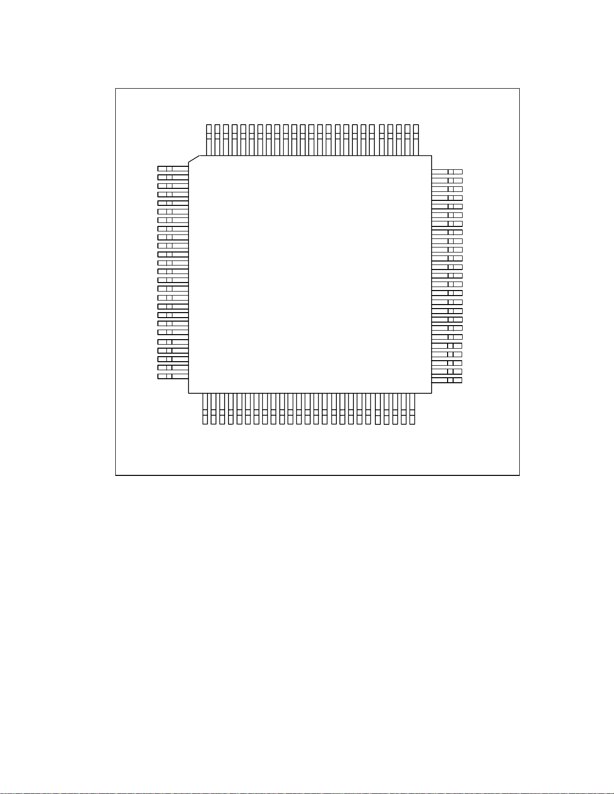
PIN CONFIGURATION
Note: Pinouts are the same for both the TQFP and STQFP Packages.
nDTR2
nCTS2
nRTS2
nDSR2
TXD2
RXD2
nDCD2
VCC
nRI2
nDCD1
nRI1
nDTR1
nCTS1
nRTS1
nDSR1
TXD1
RXD1
nSTROBE
nALF
nERROR
nACK
BUSYPESLCT
VSS
DRVDEN0
DRVDEN1
nMTR0
nDSKCHG
nDS0
GP24
VSS
nDIR
nSTEP
nWDATA
nWGATE
nHDSEL
nINDEX
nTRK0
nWRTPRT
nRDATA
nIO_PME
VTR
CLOCKI
LAD0
LAD1
LAD2
LAD3
nLFRAME
nLDRQ
9998979695949392919089888786858483828180797877
100
1
2
3
4
5
6
7
8
9
10
11
12
13
14
15
16
17
18
19
20
21
22
23
24
25
LPC47N227
100 Pin TQFP
26272829303132333435363738394041424344454647484950
VSS
GP30
GP31
GP32
GP33
GP34
GP35
GP36
GP37
GP40
GP41
GP42
GP43
GP44
GP45
GP46
nPCI_RESET
nLPCPD
PCI_CLK
SER_IRQ
nCLKRUN
76
75
74
73
72
71
70
69
68
67
66
65
64
63
62
61
60
59
58
57
56
55
54
53
52
51
GP47
GP10
GP12/nIO_SMI
GP11/SYSOPT
PD7
PD6
PD5
PD4
PD3
PD2
PD1
PD0
nSLCTIN
nINIT
VCC
GP23/FDC_PP
IRMODE/IRRX3
IRTX2
IRRX2
VSS
GP22
GP21
GP20
GP17
GP16
GP15
VCC
GP14/IRQIN2
GP13/IRQIN1
4

DESCRIPTION OF PIN FUNCTIONS
TQFP/
STQFP
PIN #
23:20 LPC Address/
Data bus 3-0
24 LPC Frame nLFRAME PCI_I Active low signal indicates start of new
25 LPC
DMA/Bus Master
Request
26 PCI RESET nPCI_RESE
27 LPC Power Down
(Note 2)
28 PCI Clock
Controller
29 PCI Clock PCI_CLK PCI_CLK PCI clock input.
30 Serial IRQ SER_IRQ PCI_IO Serial IRQ pin used with the PCI_CLK
17
Power Mgt. Event
(Note 7)
1 Drive Density 0 DRVDEN0 (O12/OD12) Indicates the drive and media selected.
2 Drive Density 1 DRVDEN1 (O12/OD12) Indicates the drive and media selected.
3 Motor On 0 nMTR0 (O12/OD12) These active low output selects motor
NAME
SYMBOL
LPC INTERFACE
BUFFER
TYPE PER
FUNCTION
1
DESCRIPTION
LAD[3:0] PCI_IO Active high LPC signals used for
multiplexed command, address and data
bus.
cycle and termination of broken cycle.
nLDRQ PCI_O Active low signal used for encoded
DMA/Bus Master request for the LPC
interface.
PCI_I Active low signal used as LPC Interface
T
Reset.
nLPCPD PCI_I Active low Power Down signal indicates
that the LPC47N227 should prepare for
power to be shut on the LPC interface.
nCLKRUN PCI_OD This signal is used to indicate the PCI
clock status and to request that a
stopped clock be started.
pin to transfer LPC47N227 interrupts to
the host.
nIO_PME
(O12/OD12) This active low Power Management Event
signal allows the LPC47N227 to request
wakeup.
FLOPPY DISK INTERFACE
Refer to configuration registers CR03,
CR0B, CR1F.
Refer to configuration registers CR03,
CR0B, CR1F.
drive 0.
4 Disk Change nDSKCHG IS This input senses that the drive door is
open or that the diskette has possibly
been changed since the last drive
selection. This input is inverted and read
via bit 7 of I/O address 3F7H. The
nDSKCHG bit also depends upon the
state of the Force Disk Change bits in the
Force FDD Status Change configuration
register (see subsection CR17 in the
Configuration section).
5 Drive Select 0 nDS0 (O12/OD12) Active low output selects drive 0.
5

TQFP/
STQFP
PIN #
8 Direction
Control
NAME
SYMBOL
BUFFER
TYPE PER
FUNCTION
nDIR (O12/OD12) This high current low active output
1
DESCRIPTION
determines the direction of the head
movement. A logic “1” on this pin means
outward motion, while a logic “0” means
inward motion.
9 Step Pulse nSTEP (O12/OD12) This active low high current driver issues a
low pulse for each track-to-track
movement of the head.
10 Write Data nWDATA (O12/OD12) This active low high current driver provides
the encoded data to the disk drive. Each
falling edge causes a flux transition on the
media.
11 Write Gate nWGATE (O12/OD12) This active low high current driver allows
current to flow through the write head. It
becomes active just prior to writing to the
diskette.
12 Head
Select
nHDSEL (O12/OD12) This high current output selects the floppy
disk side for reading or writing. A logic “1”
on this pin means side 0 will be accessed,
while a logic “0” means side 1 will be
accessed.
13 Index nINDEX
IS This active low Schmitt Trigger input
senses from the disk drive that the head is
positioned over the beginning of a track,
as marked by an index hole.
14 Track 0 nTRK0 IS This active low Schmitt Trigger input
senses from the disk drive that the head is
positioned over the outermost track.
15 Write
Protected
nWRTPRT IS This active low Schmitt Trigger input
senses from the disk drive that a disk is
write protected. Any write command is
ignored. The nWRPRT bit also depends
upon the state of the Force Write Protect
bit in the Force FDD Status Change
configuration register (see subsection
CR17 in the Configuration section).
16 Read Disk Data nRDATA IS Raw serial bit stream from the disk drive,
low active. Each falling edge represents a
flux transition of the encoded data.
SERIAL PORTS INTERFACE
84 Receive Data 1 RXD1 IS Receiver serial data input for port 1.
85 Transmit
TXD1 O12 Transmit serial data output for port 1.
Data 1
6

TQFP/
STQFP
PIN #
86 Data Set
NAME
SYMBOL
nDSR1 I
Ready 1
97 Data Set
nDSR2 I
Ready 2
87 Request to Send 1 nRTS1 O6
98 Request to Send 2 nRTS2 O6
BUFFER
TYPE PER
FUNCTION
1
DESCRIPTION
Active low Data Set Ready inputs for the
serial port. Handshake signal which
notifies the UART that the modem is ready
to establish the communication link. The
CPU can monitor the status of nDSR
signal by reading bit 5 of Modem Status
Register (MSR). A nDSR signal state
change from low to high after the last MSR
read will set MSR bit 1 to a 1. If bit 3 of
Interrupt Enable Register is set, the
interrupt is generated when nDSR
changes state.
Note: Bit 5 of MSR is the complement of
nDSR.
Active low Request to Send outputs for the
Serial Port. Handshake output signal
notifies modem that the UART is ready to
transmit data. This signal can be
programmed by writing to bit 1 of the
Modem Control Register (MCR). The
hardware reset will reset the nRTS signal
to inactive mode (high). nRTS is forced
inactive during loop mode operation.
88 Clear to
Send 1
99 Clear to
Send 2
nCTS1 I
Active low Clear to Send inputs for the
serial port. Handshake signal which
notifies the UART that the modem is ready
to receive data. The CPU can monitor the
status of nCTS signal by reading bit 4 of
Modem Status Register (MSR). A nCTS
nCTS2 I
signal state change from low to high after
the last MSR read will set MSR bit 0 to a 1.
If bit 3 of the Interrupt Enable Register is
set, the interrupt is generated when nCTS
changes state. The nCTS signal has no
effect on the transmitter.
Note: Bit 4 of MSR is the complement of
nCTS.
7

TQFP/STQFP
PIN #
89 Data Terminal
Ready 1
NAME
SYMBOL
nDTR1 O6
BUFFER
TYPE PER
FUNCTION
1
Active low Data Terminal Ready outputs for the
serial port. Handshake output signal notifies
DESCRIPTION
modem that the UART is ready to establish data
communication link. This signal can be
programmed by writing to bit 0 of Modem Control
100 Data Terminal
Ready 2
nDTR2 O6
Register (MCR). The hardware reset will reset the
nDTR signal to inactive mode (high). nDTR is
forced inactive during loop mode operation.
90 Ring
Indicator 1
(Note 8)
nRI1 I
Active low Ring Indicator inputs for the serial port.
Handshake signal which notifies the UART that the
telephone ring signal is detected by the modem.
The CPU can monitor the status of nRI signal by
reading bit 6 of Modem Status Register (MSR). A
nRI signal state change from low to high after the
92 Ring
Indicator 2
(Note 8)
nRI2 I
last MSR read will set MSR bit 2 to a 1. If bit 3 of
Interrupt Enable Register is set, the interrupt is
generated when nRI changes state.
Note: Bit 6 of MSR is the complement of nRI.
91 Data Carrier
Detect 1
nDCD1 I
Active low Data Carrier Detect inputs for the serial
port. Handshake signal which notifies the UART
that carrier signal is detected by the modem. The
CPU can monitor the status of nDCD signal by
reading bit 7 of Modem Status Register (MSR). A
94 Data Carrier
Detect 2
nDCD2 I
nDCD signal state change from low to high after
the last MSR read will set MSR bit 3 to a 1. If bit 3
of Interrupt Enable Register is set, the interrupt is
generated when nDCD changes state.
Note: Bit 7 of MSR is the complement of nDCD.
95 Receive Data 2 RXD2 IS Receiver serial data input for port 2. IR Receive
Data.
96 Transmit
Data 2
TXD2 O12 Transmit serial data output for port 2. IR transmit
data.
INFRARED INTERFACE
61 IR Receive IRRX2 IS IR Receive.
62 IR Transmit IRTX2 O12 IR Transmit.
63 IR Mode/
IR Receive 3
IRMODE/
IRRX3
O6/
IS
IR mode.
IR Receive 3.
PARALLEL PORT INTERFACE (NOTE 3)
8

TQFP/STQFP
PIN #
66 Initiate Output/
FDC Direction
NAME
SYMBOL
nINIT/
nDIR
BUFFER
TYPE PER
FUNCTION
1
(OD14/OP14)/
OD14
Control
(Note 4)
67 Printer Select
Input/
FDC Step Pulse
nSLCTIN/
nSTEP
(OD14/OP14)/
OD14
(Note 4)
68 Port Data 0/
FDC Index
69 Port Data 1/
FDC Track 0
70 Port Data 2/
FDC Write
PD0/
nINDEX
PD1/
nTRK0
PD2/
nWRTPRT
IOP14/
IS
IOP14/
IS
IOP14/
IS
Protected
71 Port Data 3/
FDC Read Disk
Data
72 Port Data 4/
FDC Disk
PD3/
nRDATA
PD4/
nDSKCHG
IOP14/
IS
IOP14/
IS
Change
73 Port Data 5 PD5 IOP14 Port Data 5
74 Port Data 6/
FDC Motor
PD6/
nMTR0
IOP14/
OD14
On 0
75 Port Data 7 PD7 IOP14 Port Data 7
77 Printer Selected
Status/
FDC Write Gate
SLCT/
nWGATE
I/
OD12
DESCRIPTION
This output is bit 2 of the printer control register.
This is used to initiate the printer when low.
Refer to Parallel Port description for use of this
pin in ECP and EPP mode.
See FDC Pin definition.
This active low output selects the printer. This is
the complement of bit 3 of the Printer Control
Register.
Refer to Parallel Port description for use of this pin
in ECP and EPP mode.
See FDC Pin definition.
Port Data 0
See FDC Pin definition.
Port Data 1
See FDC Pin definition.
Port Data 2
See FDC Pin definition.
Port Data 3
See FDC Pin definition.
Port Data 4
See FDC Pin definition.
Port Data 6
See FDC Pin definition.
This high active output from the printer indicates
that it has power on. Bit 4 of the Printer Status
Register reads the SLCT input. Refer to Parallel
Port description for use of this pin in ECP and EPP
mode.
See FDC Pin definition.
9

TQFP/STQFP
PIN #
NAME
78 Paper End/
FDC Write Data
79 Busy/
FDC Motor On 1
80 Acknowledge/
FDC Drive
Select 1
81 Error/
FDC Head
Select
82 Autofeed
Output/
FDC Density
Select 0
(Note 4)
83 Strobe Output/
FDC Drive
Select 0
(Note 4)
SYMBOL
PE/
nWRDATA
BUSY/
nMTR1
nACK/
nDS1
nERROR
nHDSEL
nALF/
nDRVDEN0
nSTROBE/
nDS0
BUFFER
TYPE PER
FUNCTION
1
I/
OD12
I/
OD12
I/
OD12
I/
OD12
(OD14/OP14)/
OD14
(OD14/OP14)/
OD14
DESCRIPTION
Another status output from the printer, a high
indicating that the printer is out of paper. Bit 5 of
the Printer Status Register reads the PE input.
Refer to Parallel Port description for use of this pin
in ECP and EPP mode.
See FDC Pin definition.
This is a status output from the printer, a high
indicating that the printer is not ready to receive
new data. Bit 7 of the Printer Status Register is the
complement of the BUSY input. Refer to Parallel
Port description for use of this pin in ECP and EPP
mode.
See FDC Pin definition.
A low active output from the printer indicating that it
has received the data and is ready to accept new
data. Bit 6 of the Printer Status Register reads the
nACK input. Refer to Parallel Port description for
use of this pin in ECP and EPP mode.
See FDC Pin definition.
A low on this input from the printer indicates that
there is a error condition at the printer. Bit 3 of the
Printer Status register reads the nERR input.
Refer to Parallel Port description for use of this pin
in ECP and EPP mode.
See FDC Pin definition.
This output goes low to cause the printer to
automatically feed one line after each line is
printed. The nALF output is the complement of bit
1 of the Printer Control Register.
Refer to Parallel Port description for use of this pin
in ECP and EPP mode.
See FDC Pin definition.
An active low pulse on this output is used to strobe
the printer data into the printer. The nSTROBE
output is the complement of bit 0 of the Printer
Control Register.
Refer to Parallel Port description for use of this pin
in ECP and EPP mode.
See FDC Pin definition.
GENERAL PURPOSE I/O
10

TQFP/STQFP
PIN #
6,
32-39, 40-47
48,
54-56,
57-59
NAME
General
Purpose I/O
(Note 9)
SYMBOL
GP24,
GP30-GP37
GP40-GP47
GP10,
GP15-GP17,
BUFFER
TYPE PER
FUNCTION
(I/O8/OD8) Dedicated General Purpose Input/Output.
1
DESCRIPTION
GP20-GP22
49 General
Purpose I/O
(System Option)
(Note 5)
(Note 9)
GP11/
(SYSOPT)
(I/O8/OD8) General Purpose Input/Output.
At the trailing edge of hardware reset the GP11 pin
is latched to determine the configuration base
address: 0 = Index Base I/O Address 02E Hex; 1 =
Index Base I/O Address 04E Hex.
50 General
Purpose I/O/
System Mgt.
GP12/
nIO_SMI
(I/O12/OD12)/
(O12/OD12)
General Purpose Input/Output.
Active low System Management Interrupt Output.
Interrupt
(Note 9)
51 General
Purpose I/O/
IRQ Input 1
(Note 9)
52 General
Purpose I/O/
IRQ Input 2
(Note 9)
64 General
Purpose I/O/
Floppy on
Parallel Port
(Note 9)
GP13/
IRQIN1
GP14/
IRQIN2
GP23/
FDC_PP
(I/O8/OD8)/
I
(I/O8/OD8)/
I
(I/O8/OD8)/
I
General Purpose Input/Output.
External Interrupt Input. Steerable onto one of the
15 Serial IRQs.
General Purpose Input/Output.
External Interrupt Input. Steerable onto one of the
15 Serial IRQs.
General Purpose Input/Output.
Floppy on the Parallel Port Indication.
CLOCK PINS
19 14MHz Clock CLOCKI IS 14.318MHz Clock Input.
POWER PINS
53,65,93 VCC (Note 6) VCC +3.3 Volt Supply Voltage.
18 VTR (Note 6) VTR +3.3 Volt Standby Voltage.
7,31, 60,76 VSS VSS Ground.
Note: The "n" as the first letter of a symbol indicates an "Active Low" signal.
Note 1: Buffer types per function on multiplexed pins are separated by a slash “/”. Buffer types in
parenthesis represent multiple buffer types for a single pin function.
Note 2: The nLPCPD pin may be tied high.
Note 3: The FDD output pins multiplexed in the PARALLEL PORT INTERFACE are OD drivers only and
are not affected by the FDD Output Driver Controls (see subsection CR05 in the Configuration
section).
Note 4: Active (push-pull) output drivers are required on these pins in the enhanced parallel port modes.
11

Note 5: The GP11/SYSOPT pin requires an external pulldown resistor to put the base IO address for
configuration at 0x02E. An external pullup resistor is required to move the base IO address
for configuration to 0x04E.
Note 6: V
CC
must not be greater than 0.5V above V
TR.
Note 7: This pin is output only and is powered by VTR.
Note 8: Ring indicator pins nRI1 and nRI2 have input buffers into the wakeup logic that are powered
by VTR. These pins are also inputs to VCC powered logic.
Note 9: GP10-GP17, GP20-GP24 and GP30-GP37 pins have input buffers into the wakeup logic that
are powered by VTR. GP40-47 pins are powered by VCC even as inputs.
Buffer Type Description
I Input TTL Compatible.
IS Input with Schmitt Trigger.
O6 Output, 6mA sink, 3mA source.
O8 Output, 8mA sink, 4mA source.
OD8 Open Drain Output, 8mA sink.
IO8 Input/Output, 8mA sink, 4mA source.
O12 Output, 12mA sink, 6mA source.
OD12 Open Drain Output, 12mA sink.
IO12 Input/Output, 12mA sink, 6mA source.
OD14 Open Drain Output, 14mA sink.
OP14 Output, 14mA sink, 14mA source.
IOP14 Input/Output, 14mA sink, 14mA source. Backdrive protected.
PCI_I Input. These pins meet the PCI 3.3V AC and DC Characteristics. (Note 1)
PCI_O Output. These pins meet the PCI 3.3V AC and DC Characteristics. (Note 1)
PCI_OD Open Drain Output. These pins meet the PCI 3.3V AC and DC Characteristics. (Note 1)
PCI_IO Input/Output. These pins meet the PCI 3.3V AC and DC Characteristics. (Note 1)
PCI_ICLK Clock Input. These pins meet the PCI 3.3V AC and DC Characteristics and timing.
(Note 2)
Note 1. See the PCI Local Bus Specification, Revision 2.1, Section 4.2.2.
Note 2. See the PCI Local Bus Specification, Revision 2.1, Section 4.2.2. and 4.2.3.
12
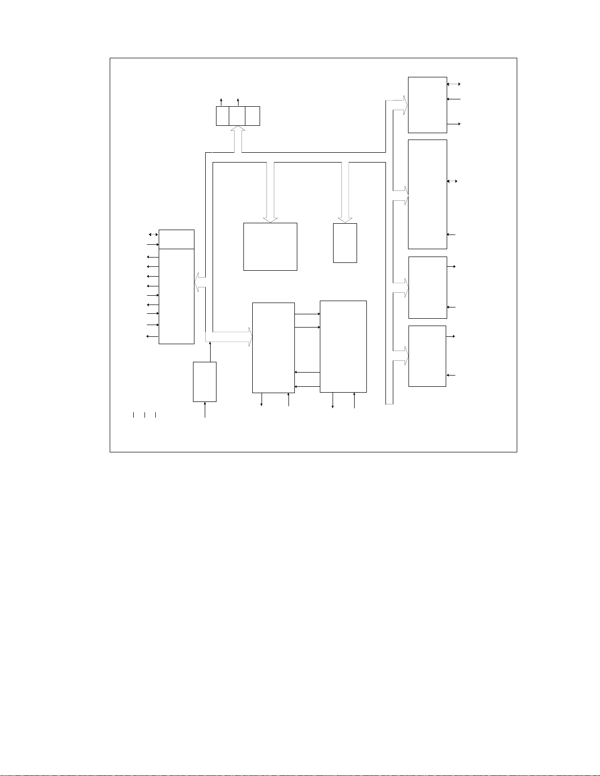
BLOCK DIAGRAM
SER_IRQ
PCI_CLK
LAD0
LAD1
LAD2
LAD3
nLFRAME
nLDRQ
nPCI_RESET
nLPCPD
nCLKRUN
SERIAL
IRQ
LPC BUS
INTERFACE
CLOCK
nIO_SMI*
GEN
nIO_PME
SMI PME WDT
CONFIGURATION
CONTROL, ADDRESS, DATA
REGISTERS
SMSC
PROPRIETARY
WDATA
WCLOCK
82077
COMPATIBLE
VERTICAL
FLOPPY DISK
CONTROLLER
CORE
RCLOCK
RDATA
BLOCK
DIGITAL
DATA
SEPERATOR
PRE-
COMPENSATION
ACPI
MULTI-MODE
PARALLEL
PORT/FDC
MUX
GENERAL
PURPOSE
I/O
16C550
COMPATIBLE
SERIAL
PORT 1
16C550
COMPATIBLE
SERIAL
PORT 2 WITH
INFRARED
INTERFACE
PD[0:7],
BUSY, SLCT,
PE, nERROR, nACK
nSLCTIN, nALF
nINIT, nSTROBE
GP10, GP11,
GP12*, GP13*,
GP14*,
GP1[5:7],
GP2[0:2],
GP23*, GP24,
GP3[0:7],
GP4[0:7]
IRQIN1*, IRQIN2*,
FDC_PP*
TXD1, nRTS1, nDTR1
nCTS1, RXD1,
nDSR1, nDCD1, nRI1
IRTX2, IRMODE*,
TXD2, nRTS2, nDTR2
IRRX2, IRRX3*,
RXD2, nCTS2,
nDSR2, nDCD2, nRI2
nMTR0, nDS0, nDIR,
V
Vcc
Vss
TR
CLOCKI
nSTEP, DRVDEN0*,
nWGATE, HDSEL,
DRVDEN1*, nWDATA
nTRK0,
nDSKCHG,
nINDEX,
nWRTPRT,
nRDATA
nWDATA nRDATA
*
Denotes Multifunction Pins
13

3.3 Volt Operation / 5 Volt Tolerance
The LPC47N227 is a 3.3 Volt part. It is intended
solely for 3.3V applications. Non-LPC bus pins
are 5V tolerant; that is, the input voltage is 5.5V
max, and the I/O buffer output pads are
backdrive protected.
The LPC interface pins are 3.3 V only. These
signals meet PCI DC specifications for 3.3V
signaling. These pins are:
!"
LAD[3:0]
!"
nLFRAME
!"
nLDRQ
!"
nLPCPD
The input voltage for all other pins is 5.5V max.
These pins include all non-LPC Bus pins and the
following pins:
!"
nPCI_RESET
!"
PCI_CLK
!"
SER_IRQ
!"
nCLKRUN
!"
nIO_PME
Power Functionality
The LPC47N227 has two power planes: VCC
and VTR.
VCC Power
The LPC47N227 is a 3.3 Volt part. The VCC
supply is 3.3 Volts (nominal). See the
Operational Description Section and the
Maximum Current Values subsection.
VTR Support
The LPC47N227 requires a trickle supply (V
to provide sleep current for the programmable
wake-up events in the PME interface when V
is removed. The VTR supply is 3.3 Volts
(nominal). See the Operational Description
Section. The maximum VTR current that is
required depends on the functions that are used
in the part. See Trickle Power Functionality
subsection and the Maximum Current Values
subsection. If the LPC47N227 is not intended to
provide wake-up capabilities on standby current,
TR
CC
)
V
can be connected to VCC. The VTR pin
TR
generates a V
Power-on-Reset signal to
TR
initialize these components.
Note: If V
wake-up events when V
is to be used for programmable
TR
is removed, VTR must
CC
be at its full minimum potential at least 10 #s
before V
and V
begins a power-on cycle. When VTR
CC
are fully powered, the potential
CC
difference between the two supplies must not
exceed 500mV.
Internal PWRGOOD
An internal PWRGOOD logical control is
included to minimize the effects of pin-state
uncertainty in the host interface as V
cycles on
CC
and off. When the internal PWRGOOD signal is
“1” (active), V
> 2.3V (nominal), and the
CC
LPC47N227 host interface is active. When the
internal PWRGOOD signal is “0” (inactive), V
$
2.3V (nominal), and the LPC47N227 host
CC
interface is inactive; that is, LPC bus reads and
writes will not be decoded.
The LPC47N227 device pins nIO_PME, nRI1,
nRI2, and most GPIOs (as input) are part of the
PME interface and remain active when the
internal PWRGOOD signal has gone inactive,
provided V
is powered. See Trickle Power
TR
Functionality section.
Trickle Power Functionality
When the LPC47N227 is running under VTR
only, the PME wakeup events are active and (if
enabled) able to assert the nIO_PME pin active
low. The following lists the wakeup events:
!"
UART 1 Ring Indicator
!"
UART 2 Ring Indicator
!"
GPIOs for wakeup. See below.
The following requirements apply to all I/O pins
that are specified to be 5 volt tolerant.
!"
I/O buffers that are wake-up event
compatible are powered by VCC. Under
VTR power (VCC=0), these pins may only
be configured as inputs. These pins have
input buffers into the wakeup logic that are
powered by VTR.
14

!"
I/O buffers that may be configured as either
push-pull or open drain under VTR power
(VCC=0), are powered by VTR. This means
they will, at a minimum, source their
specified current from VTR even when VCC
is present. This applies to the nIO_PME pin
only.
The GPIOs that are used for PME wakeup inputs
are GP10-GP17, GP20-GP24, GP30-GP37.
These GPIOs function as follows:
!"
Buffers are powered by VCC, but in the
absence of VCC they are backdrive
protected (they do not impose a load on any
external VTR powered circuitry). They are
wakeup compatible as inputs under VTR
power. These pins have input buffers into
the wakeup logic that are powered by VTR.
All GPIOs listed above are for PME wakeup as a
GPIO function (or alternate function).
See the Table in the GPIO section for more
information.
The following list summarizes the blocks,
registers and pins that are powered by VTR.
!"
PME interface block
!"
Runtime register block (includes all PME,
SMI, GP data registers)
!"
Pins for PME Wakeup:
-
GPIOs (GP10-GP17, GP20-GP24,
GP30-GP37) as input
-
nIO_PME as input
-
nRI1, nRI2 as input
Maximum Current Values
See the “Operational Description” section for the
maximum current values.
The maximum VTR current, I
, is given with all
TR
outputs open (not loaded), and all inputs in a
fixed state (i.e., 0V or 3.3V). The total maximum
current for the part is the unloaded value PLUS
the maximum current sourced by the pin that is
driven by VTR. The pin that is powered by VTR
(as output) is nIO_PME. This pin, if configured
as a push-pull output, will source a minimum of
6mA at 2.4V when driving.
The maximum VCC current, I
, is given with all
CC
outputs open (not loaded), and all inputs in a
fixed state (i.e., 0V or 3.3V).
Power Management Events (PME/SCI)
The LPC47N227 offers support for Power
Management Events (PMEs), also referred to as
System Control Interrupt (SCI) events. The
terms PME and SCI are used synonymously
throughout this document to refer to the
indication of an event to the chipset via the
assertion of the nIO_PME output signal on pin
17. See the “PME Support” section. Do not
connect the nIO_PME pin to PCI PME pins.
15

FUNCTIONAL DESCRIPTION
Super I/O Registers
The address map, shown below in Table 1,
shows the addresses of the different blocks of
the Super I/O immediately after power up. The
base addresses of the FDC, serial and parallel
ports, runtime register block and configuration
register block can be moved via the
configuration registers. Some addresses are
used to access more than one register.
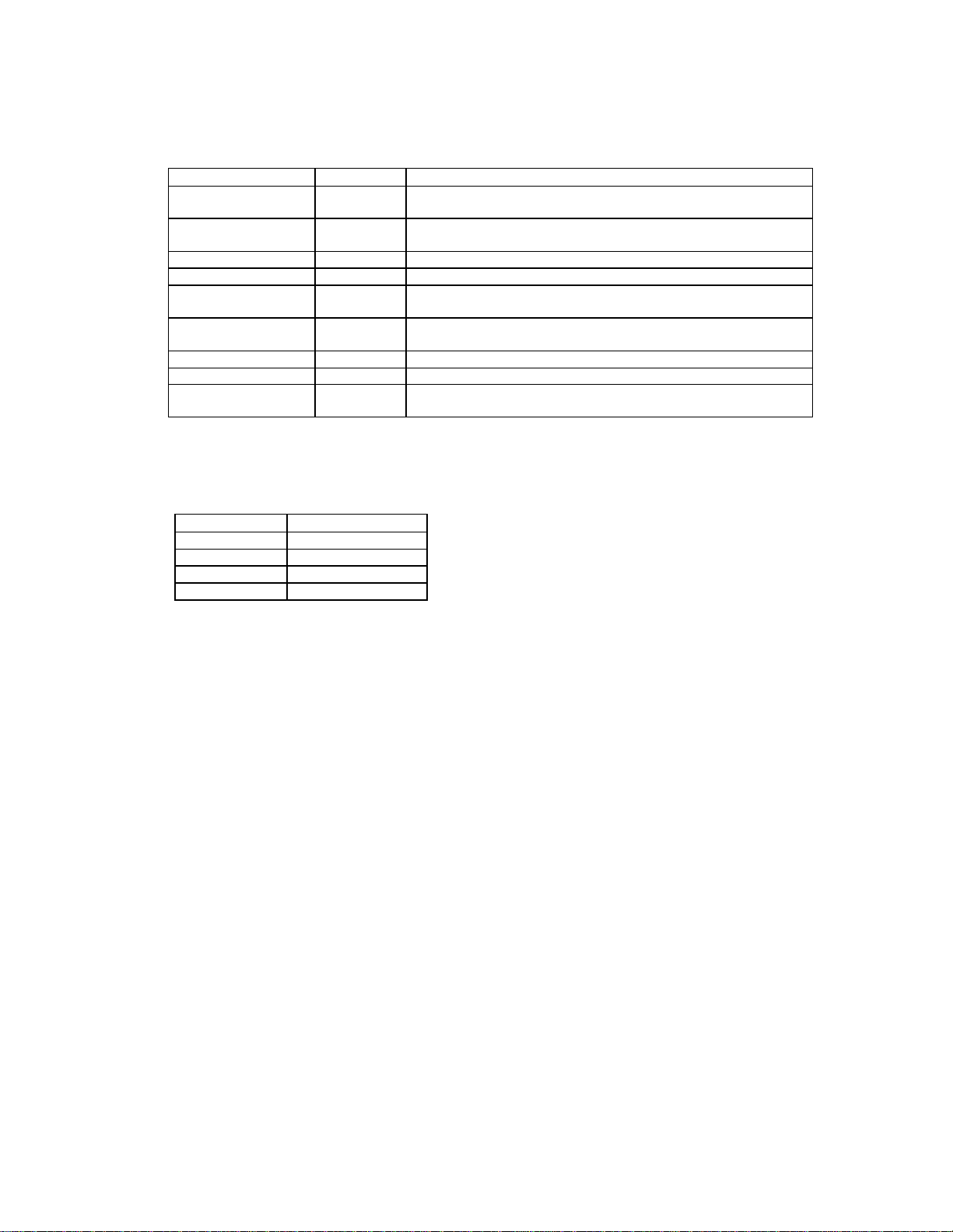
Table 1 - Super I/O Block Addresses
ADDRESS
Base+(0-5) and +(7) Floppy Disk
Base+(0-7) Serial Port Com 1
Base1+(0-7)
Base2+(0-7)
Base+(0-3)
Base+(0-7)
Base+(0-3), +(400-402)
Base+(0-7), +(400-402)
Base + (0-F) Runtime Registers
Base + (0-1) Configuration
Note 1: Refer to the configuration register descriptions for setting the base address.
Serial Port Com 2 IR Support
Parallel Port
SPP
EPP
ECP
ECP+EPP+SPP
Host Processor Interface (LPC)
The host processor communicates with the
LPC47N227 through a series of read/write
registers via the LPC interface. The port
addresses for these registers are shown in Table
1. Register access is accomplished through I/O
cycles or DMA transfers. All registers are 8 bits
wide.
BLOCK NAME
NOTES
FIR and CIR
16
LPC Interface
The following sub-sections specify the
implementation of the LPC bus.
SIGNAL NAME TYPE DESCRIPTION
LAD[3:0] I/O LPC address/data bus. Multiplexed command, address and
data bus.
nLFRAME Input Frame signal. Indicates start of new cycle and termination of
broken cycle
nPCI_RESET Input PCI Reset. Used as LPC Interface Reset.
nLDRQ Output Encoded DMA/Bus Master request for the LPC interface.
nIO_PME OD Power Mgt Event signal. Allows the LPC47N227 to request
wakeup.
nLPCPD Input Powerdown Signal. Indicates that the LPC47N227 should
prepare for power to be shut on the LPC interface.
SER_IRQ I/O Serial IRQ.
PCI_CLK Input PCI Clock.
nCLKRUN I/OD Clock Run. Allows the LPC47N227 to request the stopped
PCI_CLK be started.
LPC Cycles
The following cycle types are supported by the
LPC protocol.
CYCLE TYPE TRANSFER SIZE
I/O Write 1 Byte
I/O Read 1 Byte
DMA Write 1 Byte
DMA Read 1 Byte
The LPC47N227 ignores cycles that it does not
support.
Field Definitions
The data transfers are based on specific fields
that are used in various combinations,
depending on the cycle type. These fields are
driven onto the LAD[3:0] signal lines to
communicate address, control and data
information over the LPC bus between the host
and the LPC47N227. See the
Low Pin
LPC Interface Signal Definition
The signals required for the LPC bus interface
are described in the table below. LPC bus
signals use PCI 33MHz electrical signal
characteristics.
Count (LPC) Interface Specification
from Intel, Section 4.2 for definition of these
fields.
nLFRAME Usage
nLFRAME is used by the host to indicate the
start of cycles and the termination of cycles due
to an abort or time-out condition. This signal is
to be used by the LPC47N227 to know when to
monitor the bus for a cycle.
This signal is used as a general notification that
the LAD[3:0] lines contain information relative to
the start or stop of a cycle, and that the
LPC47N227 monitors the bus to determine
whether the cycle is intended for it. The use of
nLFRAME allows the LPC47N227 to enter a
lower power state internally. There is no need
for the LPC47N227 to monitor the bus when it is
inactive, so it can decouple its state machines
from the bus, and internally gate its clocks.
When the LPC47N227 samples nLFRAME
active, it immediately stops driving the LAD[3:0]
signal lines on the next clock and monitor the
bus for new cycle information.
Revision 1.0
17

The nLFRAME signal functions as described in
the Low Pin Count (LPC) Interface Specification
Revision 1.0.
I/O Read and Write Cycles
The LPC47N227 is the target for I/O cycles. I/O
cycles are initiated by the host for register or
FIFO accesses, and will generally have minimal
Sync times. The minimum number of wait-states
between bytes is 1. EPP cycles will depend on
the speed of the external device, and may have
much longer Sync times.
Data transfers are assumed to be exactly 1-byte.
If the CPU requested a 16 or 32-bit transfer, the
host will break it up into 8-bit transfers.
See the
Specification
sequence of cycles for the I/O Read and Write
cycles.
DMA Read and Write Cycles
Low Pin Count (LPC) Interface
Reference, Section 5.2, for the
DMA read cycles involve the transfer of data
from the host (main memory) to the LPC47N227.
DMA write cycles involve the transfer of data
from the LPC47N227 to the host (main memory).
Data will be coming from or going to a FIFO and
will have minimal Sync times. Data transfers
to/from the LPC47N227 are 1 byte.
See the
Specification
definitions and the sequence of the DMA Read
and Write cycles.
DMA Protocol
DMA on the LPC bus is handled through the use
of the nLDRQ line from the LPC47N227 and
special encodings on LAD[3:0] from the host.
The DMA mechanism for the LPC bus is
described in the Low Pin Count (LPC)
Specification Revision 1.0.
Low Pin Count (LPC) Interface
Reference, Section 6.4, for the field
18

Power Management
CLOCKRUN Protocol
See the
Specification
LPCPD Protocol
The LPC47N227 will function properly if the
nLPCPD signal goes active and then inactive
again without nPCI_RESET becoming active.
This is a requirement for notebook power
management functions.
Although the LPC Bus spec 1.0 section 8.2
states, "After nLPCPD goes back inactive, the
LPC I/F will always be reset using nLRST”, this
statement does not apply for mobile systems.
nLRST (nPCI_RESET) will not occur if the LPC
Bus power was not removed. For example,
when exiting a "light" sleep state (ACPI S1, APM
POS), nLRST (nPCI_RESET) will not occur.
When exiting a "deeper" sleep state (ACPI S3S5, APM STR, STD, soft-off), nLRST
(nPCI_RESET) will occur.
The nLPCPD pin is implemented as a “local”
powergood for the LPC interface in the
LPC47N227. It is not used as a global
powergood for the chip. It is used to reset the
LPC block and hold it in reset.
An internal powergood is implemented in
LPC47N227 to minimize power dissipation in the
entire chip.
Prior to going to a low-power state, the system
will assert the nLPCPD signal. It will go active at
least 30 microseconds prior to the LCLK
(PCI_CLK) signal stopping low and power being
shut to the other LPC I/F signals.
Upon recognizing nLPCPD active, the
LPC47N227 will tri-state the nLDRQ signal and
do so until nLPCPD goes back active.
Upon recognizing nLPCPD inactive, the
LPC47N227 will drive its nLDRQ signal high.
Low Pin Count (LPC) Interface
Reference, Section 8.1.
See the
Specification
SYNC Protocol
See the
Specification
table of valid SYNC values.
Typical Usage
The SYNC pattern is used to add wait states.
For read cycles, the LPC47N227 immediately
drives the SYNC pattern upon recognizing the
cycle. The host immediately drives the sync
pattern for write cycles. If the LPC47N227 needs
to assert wait states, it does so by driving 0101
or 0110 on LAD[3:0] until it is ready, at which
point it will drive 0000 or 1001. The LPC47N227
will choose to assert 0101 or 0110, but not
switch between the two patterns.
The data (or wait state SYNC) will immediately
follow the 0000 or 1001 value.
The SYNC value of 0101 is intended to be used
for normal wait states, wherein the cycle will
complete within a few clocks. The LPC47N227
uses a SYNC of 0101 for all wait states in a
DMA transfer.
The SYNC value of 0110 is intended to be used
where the number of wait states is large. This is
provided for EPP cycles, where the number of
wait states could be quite large (>1
microsecond). However, the LPC47N227 uses a
SYNC of 0110 for all wait states in an I/O
transfer.
The SYNC value is driven within 3 clocks.
Low Pin Count (LPC) Interface
Reference, Section 8.2.
Low Pin Count (LPC) Interface
Reference, Section 4.2.1.8 for a
19

SYNC Timeout
The SYNC value is driven within 3 clocks. If the
host observes 3 consecutive clocks without a
valid SYNC pattern, it will abort the cycle.
The LPC47N227 does not assume any particular
timeout. When the host is driving SYNC, it may
have to insert a very large number of wait states,
depending on PCI latencies and retries.
SYNC Patterns and Maximum Number of
SYNCS
If the SYNC pattern is 0101, then the host
assumes that the maximum number of SYNCs is
8.
If the SYNC pattern is 0110, then no maximum
number of SYNCs is assumed. The LPC47N227
has protection mechanisms to complete the
cycle. This is used for EPP data transfers and
will utilize the same timeout protection that is in
EPP.
SYNC Error Indication
The LPC47N227 reports errors via the LAD[3:0]
= 1010 SYNC encoding.
If the host was reading data from the
LPC47N227, data will still be transferred in the
next two nibbles. This data may be invalid, but it
will be transferred by the LPC47N227. If the
host was writing data to the LPC47N227, the
data had already been transferred.
In the case of multiple byte cycles, such as DMA
cycles, an error SYNC terminates the cycle.
Therefore, if the host is transferring 4 bytes from
a device, if the device returns the error SYNC in
the first byte, the other three bytes will not be
transferred.
I/O and DMA START Fields
I/O and DMA cycles use a START field of 0000.
Reset Policy
The following rules govern the reset policy:
1) When nPCI_RESET goes inactive (high),
the clock is assumed to have been running
for 100usec prior to the removal of the reset
signal, so that everything is stable. This is
the same reset active time after clock is
stable that is used for the PCI bus.
2) When nPCI_RESET goes active (low):
a) The host drives the nLFRAME signal
high, tristates the LAD[3:0] signals, and
ignores the nLDRQ signal.
b) The LPC47N227 ignores nLFRAME, tri-
states the LAD[3:0] pins and drives the
nLDRQ signal inactive (high).
LPC Transfers
Wait State Requirements
I/O Transfers
The LPC47N227 inserts three wait states for an
I/O read and two wait states for an I/O write
cycle. A SYNC of 0110 is used for all I/O
transfers. The exception to this is for transfers
where IOCHRDY would be deasserted in an ISA
transfer (i.e., EPP or IrCC transfers) in which
case the sync pattern of 0110 is used and a
large number of syncs may be inserted (up to
330 which corresponds to a timeout of 10us).
DMA Transfers
The LPC47N227 inserts three wait states for a
DMA read and four wait states for a DMA write
cycle. A SYNC of 0101 is used for all DMA
transfers.
See the example timing for the LPC cycles in the
“Timing Diagrams” section.
20

FLOPPY DISK CONTROLLER
The Floppy Disk Controller (FDC) provides the
interface between a host microprocessor and the
floppy disk drives. The FDC integrates the
functions of the Formatter/Controller, Digital Data
Separator, Write Precompensation and Data Rate
Selection logic for an IBM XT/AT compatible FDC.
The true CMOS 765B core guarantees 100% IBM
PC XT/AT compatibility in addition to providing
data overflow and underflow protection.
The FDC is compatible to the 82077AA using
SMSC's proprietary floppy disk controller core.
The LPC47N227 supports one floppy disk drive
directly through the FDC interface pins and two
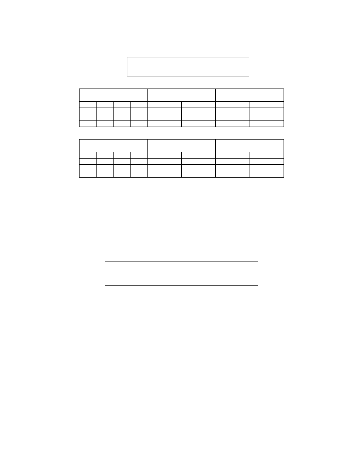
Table 2 – Status, Data and Control Registers
(Shown with base addresses of 3F0 and 370)
PRIMARY
ADDRESS
3F0
3F1
3F2
3F3
3F4
3F4
3F5
3F6
3F7
3F7
Status Register A (SRA)
Address 3F0 READ ONLY
This register is read-only and monitors the state
of the internal interrupt signal and several disk
SECONDARY
ADDRESS
370
371
372
373
374
374
375
376
377
377
R/W
R/W
R/W
W
R/W
W
floppy disk drives via the FDC interface on the
parallel port pins. It can also be configured to
support one drive on the FDC interface pins and
one drive on the parallel port pins.
FDC Internal Registers
The Floppy Disk Controller contains eight internal
registers that facilitate the interfacing between the
host microprocessor and the disk drive. Table 2
shows the addresses required to access these
registers. Registers other than the ones shown
are not supported. The rest of the description
assumes that the primary addresses have been
selected.
Status Register A (SRA)
R
Status Register B (SRB)
R
Digital Output Register (DOR)
Tape Drive Register (TDR)
Main Status Register (MSR)
R
Data Rate Select Register (DSR)
Data (FIFO)
Reserved
Digital Input Register (DIR)
R
Configuration Control Register (CCR)
interface pins in PS/2 and Model 30 modes. The
SRA can be accessed at any time when in PS/2
mode. In the PC/AT mode the data bus pins D0
- D7 are held in a high impedance state for a
read of address 3F0.
REGISTER
21

PS/2 Mode
7 6 5 4 3 2 1 0
INT
PENDING
RESET
COND.
BIT 0 DIRECTION
Active high status indicating the direction of head movement. A logic "1" indicates inward direction; a logic
"0" indicates outward direction.
BIT 1 nWRITE PROTECT
Active low status of the WRITE PROTECT disk interface input. A logic "0" indicates that the disk is write
protected.
BIT 2 nINDEX
Active low status of the INDEX disk interface input.
BIT 3 HEAD SELECT
Active high status of the HDSEL disk interface input. A logic "1" selects side 1 and a logic "0" selects side
0.
BIT 4 nTRACK 0
Active low status of the TRK0 disk interface input.
BIT 5 STEP
Active high status of the STEP output disk interface output pin.
BIT 6 nDRV2
This function is not supported. This bit is always read as “1”.
BIT 7 INTERRUPT PENDING
Active high bit indicating the state of the Floppy Disk Interrupt output.
PS/2 Model 30 Mode
BIT 0 nDIRECTION
Active low status indicating the direction of head movement. A logic "0" indicates inward direction; a logic
"1" indicates outward direction.
7 6 5 4 3 2 1 0
INT
RESET
COND.
0 1 0 N/A 0 N/A N/A 0
PENDING
0 0 0 N/A 1 N/A N/A 1
nDRV2 STEP nTRK0 HDSEL nINDX nWP DIR
DRQ STEP
F/F
TRK0 nHDSEL INDX WP nDIR
22

BIT 1 WRITE PROTECT
Active high status of the WRITE PROTECT disk interface input. A logic "1" indicates that the disk is write
protected.
BIT 2 INDEX
Active high status of the INDEX disk interface input.
BIT 3 nHEAD SELECT
Active low status of the HDSEL disk interface input. A logic "0" selects side 1 and a logic "1" selects side
0.
BIT 4 TRACK 0
Active high status of the TRK0 disk interface input.
BIT 5 STEP
Active high status of the latched STEP disk interface output pin. This bit is latched with the STEP output
going active, and is cleared with a read from the DIR register, or with a hardware or software reset.
BIT 6 DMA REQUEST
Active high status of the DMA request pending.
BIT 7 INTERRUPT PENDING
Active high bit indicating the state of the Floppy Disk Interrupt.
Status Register B (SRB)
Address 3F1 READ ONLY
This register is read-only and monitors the state of several disk interface pins in PS/2 and model 30
modes. The SRB can be accessed at any time when in PS/2 mode. In the PC/AT mode the data bus pins
D0 - D7 are held in a high impedance state for a read of address 3F1.
PS/2 Mode
BIT 0 MOTOR ENABLE 0
Active high status of the MTR0 disk interface output pin. This bit is low after a hardware reset and
unaffected by a software reset.
BIT 1 MOTOR ENABLE 1
Active high status of the MTR1 disk interface output pin. This bit is low after a hardware reset and
unaffected by a software reset.
BIT 2 WRITE GATE
Active high status of the WGATE disk interface output.
7 6 5 4 3 2 1 0
1 1 DRIVE
RESET
COND.
WDATA
SEL0
1 1 0 0 0 0 0 0
TOGGLE
RDATA
TOGGLE
WGATE MOT
EN1
MOT
EN0
23

BIT 3 READ DATA TOGGLE
Every inactive edge of the RDATA input causes this bit to change state.
BIT 4 WRITE DATA TOGGLE
Every inactive edge of the WDATA input causes this bit to change state.
BIT 5 DRIVE SELECT 0
Reflects the status of the Drive Select 0 bit of the DOR (address 3F2 bit 0). This bit is cleared after a
hardware reset and it is unaffected by a software reset.
BIT 6 RESERVED
Always read as a logic "1".
BIT 7 RESERVED
Always read as a logic "1".
PS/2 Model 30 Mode
7 6 5 4 3 2 1 0
nDRV2 nDS1 nDS0 WDATA
RESET
COND.
BIT 0 nDRIVE SELECT 2
The DS2 disk interface is not supported.
BIT 1 nDRIVE SELECT 3
The DS3 disk interface is not supported.
BIT 2 WRITE GATE
Active high status of the latched WGATE output signal. This bit is latched by the active going edge of
WGATE and is cleared by the read of the DIR register.
BIT 3 READ DATA
Active high status of the latched RDATA output signal. This bit is latched by the inactive going edge of
RDATA and is cleared by the read of the DIR register.
BIT 4 WRITE DATA
Active high status of the latched WDATA output signal. This bit is latched by the inactive going edge of
WDATA and is cleared by the read of the DIR register. This bit is not gated with WGATE.
BIT 5 nDRIVE SELECT 0
Active low status of the DS0 disk interface output.
BIT 6 nDRIVE SELECT 1
Active low status of the DS1 disk interface output.
BIT 7 nDRV2
Active low status of the DRV2 disk interface input. Note: This function is not supported.
RDATA
F/F
N/A 1 1 0 0 0 1 1
24
F/F
WGATE
F/F
nDS3 nDS2

Digital Output Register (DOR)
Address 3F2 READ/WRITE
The DOR controls the drive select and motor enables of the disk interface outputs. It also contains the
enable for the DMA logic and a software reset bit. The contents of the DOR are unaffected by a software
reset. The DOR can be written to at any time.
7 6 5 4 3 2 1 0
MOT
RESET
COND.
BIT 0 and 1 DRIVE SELECT
These two bits are binary encoded for the drive selects, thereby allowing only one drive to be selected at
one time.
BIT 2 nRESET
A logic "0" written to this bit resets the Floppy disk controller. This reset will remain active until a logic "1"
is written to this bit. This software reset does not affect the DSR and CCR registers, nor does it affect the
other bits of the DOR register. The minimum reset duration required is 100ns, therefore toggling this bit by
consecutive writes to this register is a valid method of issuing a software reset.
BIT 3 DMAEN
PC/AT and Model 30 Mode:
Writing this bit to logic "1" will enable the DMA and interrupt functions. This bit being a logic "0" will
disable the DMA and interrupt functions. This bit is a logic "0" after a reset and in these modes.
PS/2 Mode: In this mode the DMA and interrupt functions are always enabled. During a reset, this bit will
be cleared to a logic "0".
BIT 4 MOTOR ENABLE 0
This bit controls the MTR0 disk interface output. A logic "1" in this bit will cause the output pin to go active.
BIT 5 MOTOR ENABLE 1
This bit controls the MTR1 disk interface output. A logic "1" in this bit will cause the output pin to go active.
MOT
EN3
0 0 0 0 0 0 0 0
EN2
MOT
EN1
MOT
EN0
DMAEN nRESET DRIVE
SEL1
DRIVE
SEL0
25
BIT 6 MOTOR ENABLE 2
The MTR2 disk interface output is not supported.
BIT 7 MOTOR ENABLE 3
The MTR3 disk interface output is not supported.
DIGITAL OUTPUT
REGISTER
Bit 5 Bit 4 Bit1 Bit 0 nDS1 nDS0 nMTR1 nMTR0
X 1 0 0 1 0 nBIT 5 nBIT 4
1 X 0 1 0 1 nBIT 5 nBIT 4
0 0 X X 1 1 nBIT 5 nBIT 4
DIGITAL OUTPUT
REGISTER
Bit 5 Bit 4 Bit1 Bit 0 nDS1 nDS0 nMTR1 nMTR0
X 1 0 0 0 1 nBIT 4 nBIT 5
1 X 0 1 1 0 nBIT 4 nBIT 5
0 0 X X 1 1 nBIT 4 nBIT 5
Tape Drive Register (TDR)
Address 3F3 READ/WRITE
The Tape Drive Register (TDR) is included for 82077 software compatibility and allows the user to assign
tape support to a particular drive during initialization. Any future references to that drive automatically
invokes tape support. The TDR Tape Select bits TDR.[1:0] determine the tape drive number. Table 5
illustrates the Tape Select Bit encoding. Note that drive 0 is the boot device and cannot be assigned tape
support. The remaining Tape Drive Register bits TDR.[7:2] are tristated when read. The TDR is
unaffected by a software reset.
Note: The LPC47N227 supports one floppy drive directly on the FDC interface pins and two floppy drives
on the Parallel Port.
Normal Floppy Mode
DRIVE
0
1
Table 3 – Internal 2 Drive Decode (Normal)
DRIVE SELECT OUTPUTS
Table 4 – Internal 2 Drive Decode (Drives 0 and 1 Swapped)
TAPE SEL1
(TDR.1)
0
0
1
1
(ACTIVE LOW)
DRIVE SELECT OUTPUTS
(ACTIVE LOW)
Table 5 – Tape Select Bits
TAPE SEL0
(TDR.0)
0
1
0
1
26
DOR VALUE
1CH
2DH
MOTOR ON OUTPUTS
DRIVE SELECTED
(ACTIVE LOW)
MOTOR ON OUTPUTS
(ACTIVE LOW)
None
1
2
3
Normal mode. Register 3F3 contains only bits 0 and 1. When this register is read, bits 2 - 7 are ‘0’.
DB7 DB6 DB5 DB4 DB3 DB2 DB1 DB0
REG 3F3 0 0 0 0 0 0 tape sel1 tape sel0
Enhanced Floppy Mode 2 (OS2)
Register 3F3 for Enhanced Floppy Mode 2 operation.
DB7 DB6 DB5 DB4 DB3 DB2 DB1 DB0
REG 3F3 Reserved Reserved Drive Type ID Floppy Boot Drive tape sel1 tape sel0
Table 6 – Drive Type ID
DIGITAL OUTPUT REGISTER REGISTER 3F3 - DRIVE TYPE ID
Bit 1 Bit 0 Bit 5 Bit 4
0 0 CR06 - B1 CR06 - B0
0 1 CR06 - B3 CR06 - B2
1 0 CR06 - B5 CR06 - B4
1 1 CR06 - B7 CR06 - B6
Note: CR06-Bx = Configuration Register 06, Bit x.
Data Rate Select Register (DSR)
Address 3F4 WRITE ONLY
This register is write only. It is used to program the data rate, amount of write precompensation, power
down status, and software reset. The data rate is programmed using the Configuration Control Register
(CCR) not the DSR, for PC/AT and PS/2 Model 30 applications. Other applications can set the data rate
in the DSR. The data rate of the floppy controller is the most recent write of either the DSR or CCR. The
DSR is unaffected by a software reset. A hardware reset will set the DSR to 02H, which corresponds to
the default precompensation setting and 250 Kbps.
7 6 5 4 3 2 1 0
S/W
RESET
RESET
COND.
BIT 0 and 1 DATA RATE SELECT
These bits control the data rate of the floppy controller. See Table 8 for the settings corresponding to the
individual data rates. The data rate select bits are unaffected by a software reset, and are set to 250 Kbps
after a hardware reset.
BIT 2 through 4 PRECOMPENSATION SELECT
These three bits select the value of write precompensation that will be applied to the WDATA output
signal. Table 7 shows the precompensation values for the combination of these bits settings. Track 0 is
the default starting track number to start precompensation. This starting track number can be changed by
the configure command.
POWER
DOWN
0 0 0 0 0 0 1 0
0 PRE-
COMP2
27
PRE-
COMP1
PRE-
COMP0
DRATE
SEL1
DRATE
SEL0
BIT 5 UNDEFINED
Should be written as a logic "0".
BIT 6 LOW POWER
A logic "1" written to this bit will put the floppy controller into manual low power mode. The floppy
controller clock and data separator circuits will be turned off. The controller will come out of manual low
power mode after a software reset or access to the Data Register or Main Status Register.
BIT 7 SOFTWARE RESET
This active high bit has the same function as the DOR RESET (DOR bit 2) except that this bit is self
clearing.
Note: The DSR is Shadowed in the Floppy Data Rate Select Shadow Register, located in the
Configuration section (CR14).
Table 7 – Precompensation Delays
PRECOMP
432
<2Mbps 2Mbps
111
001
010
011
100
101
110
000
Default: See Table 10
PRECOMPENSATION
DELAY (nsec)
0.00
41.67
83.34
125.00
166.67
208.33
250.00
Default
0
20.8
41.7
62.5
83.3
104.2
125
Default
Table 8 – Data Rates
DRIVE RATE DATA RATE DATA RATE
DRATE(1)
DENSEL
DRT1 DRT0 SEL1 SEL0 MFM FM 1 0
0 0 1 1 1Meg --- 1 1 1
0 0 0 0 500 250 1 0 0
0 0 0 1 300 150 0 0 1
0 0 1 0 250 125 0 1 0
0 1 1 1 1Meg --- 1 1 1
0 1 0 0 500 250 1 0 0
0 1 0 1 500 250 0 0 1
0 1 1 0 250 125 0 1 0
1 0 1 1 1Meg --- 1 1 1
1 0 0 0 500 250 1 0 0
1 0 0 1 2Meg --- 0 0 1
1 0 1 0 250 125 0 1 0
Drive Rate Table (Recommended) 00 = 360K, 1.2M, 720K, 1.44M and 2.88M Vertical Format
01 = 3-Mode Drive
10 = 2 Meg Tape
Note 1: The DRATE and DENSEL values are mapped onto the DRVDEN pins.
28
Table 9 – DRVDEN Mapping0
DT1 DT0 DRVDEN1 (1) DRVDEN0 (1) DRIVE TYPE
0 0 DRATE0 DENSEL 4/2/1 MB 3.5"
2/1 MB 5.25" FDDS
2/1.6/1 MB 3.5" (3-MODE)
1 0 DRATE0 DRATE1
0 1 DRATE0 nDENSEL PS/2
1 1 DRATE1 DRATE0
Table 10 – Default Precompensation Delays
DATA RATE
2 Mbps
1 Mbps
500 Kbps
300 Kbps
250 Kbps
Main Status Register (MSR)
Address 3F4 READ ONLY
The Main Status Register is a read-only register and indicates the status of the disk controller. The Main
Status Register can be read at any time. The MSR indicates when the disk controller is ready to receive
data via the Data Register. It should be read before each byte transferring to or from the data register
except in DMA mode. No delay is required when reading the MSR after a data transfer.
7 6 5 4 3 2 1 0
RQM
BIT 0 - 1 DRV x BUSY
These bits are set to 1s when a drive is in the seek portion of a command, including implied and
overlapped seeks and recalibrates.
BIT 4 COMMAND BUSY
This bit is set to a 1 when a command is in progress. This bit will go active after the command byte has
been accepted and goes inactive at the end of the results phase. If there is no result phase (Seek,
Recalibrate commands), this bit is returned to a 0 after the last command byte.
BIT 5 NON-DMA
This mode is selected in the SPECIFY command and will be set to a 1 during the execution phase of a
command. This is for polled data transfers and helps differentiate between the data transfer phase and
the reading of result bytes.
BIT 6 DIO
Indicates the direction of a data transfer once a RQM is set. A 1 indicates a read and a 0 indicates a write
is required.
DIO
NON
DMA
CMD
BUSY Reserved Reserved
PRECOMPENSATIO
N DELAYS
20.8 ns
41.67 ns
125 ns
125 ns
125 ns
DRV1
BUSY
DRV0
BUSY
29

BIT 7 RQM
Indicates that the host can transfer data if set to a 1. No access is permitted if set to a 0.
Data Register (FIFO)
Address 3F5 READ/WRITE
All command parameter information, disk data and result status are transferred between the host
processor and the floppy disk controller through the Data Register.
Data transfers are governed by the RQM and DIO bits in the Main Status Register.
The Data Register defaults to FIFO disabled mode after any form of reset. This maintains PC/AT
hardware compatibility. The default values can be changed through the Configure command (enable full
FIFO operation with threshold control). The advantage of the FIFO is that it allows the system a larger
DMA latency without causing a disk error. Table 11 gives several examples of the delays with a FIFO.
The data is based upon the following formula:
Threshold
# x
At the start of a command, the FIFO action is always disabled and command parameters are sent based
upon the RQM and DIO bit settings. As the command execution phase is entered, the FIFO is cleared of
any data to ensure that invalid data is not transferred.
An overrun or underrun will terminate the current command and the transfer of data. Disk writes will
complete the current sector by generating a 00 pattern and valid CRC. Reads require the host to remove
the remaining data so that the result phase may be entered.
1
DATA
RATE
x 8
FIFO THRESHOLD
FIFO THRESHOLD
- 1.5 #s =
DELAY
EXAMPLES
1 byte
2 bytes
8 bytes
15 bytes
EXAMPLES
1 byte
2 bytes
8 bytes
15 bytes
Table 11 – FIFO Service Delay
MAXIMUM DELAY TO SERVICING AT
2 Mbps DATA RATE
1 x 4 #s - 1.5 #s = 2.5 #s
2 x 4 #s - 1.5 #s = 6.5 #s
8 x 4 #s - 1.5 #s = 30.5 #s
15 x 4 #s - 1.5 #s = 58.5 #s
MAXIMUM DELAY TO SERVICING AT
1 Mbps DATA RATE
1 x 8 #s - 1.5 #s = 6.5 #s
2 x 8 #s - 1.5 #s = 14.5 #s
8 x 8 #s - 1.5 #s = 62.5 #s
15 x 8 #s - 1.5 #s = 118.5 #s
30
 Loading...