


LPC47N217
64-Pin Super I/O with LPC
Interface
Datasheet
Product Features
3.3 Volt Operation (5V tolerant)
Programmable Wakeup Event Interface
(IO_PME# Pin)
SMI Support (IO_SMI# Pin)
GPIOs (14)
Two IRQ Input Pins
XNOR Chain
PC99a, PC2001
ACPI 2.0 Compliant
64-pin STQFP Packages (2mm footprint)
Intelligent Auto Power Management
Serial Ports
− One Full Function Serial Port
− High Speed 16C550A Compatible UART with
Send/Receive 16-Byte FIFO
− Supports 230k and 460k Baud
− Programmable Baud Rate Generator
− Modem Control Circuitry
Infrared Communications Controller
− IrDA v1.2 (4Mbps), HPSIR, ASKIR, Consumer IR
Support
− 1 IR Port
− 96 Base I/O Address, 15 IRQ Options and 3 DMA
Options
Multi-Mode Parallel Port with ChiProtect™
− Standard Mode IBM PC/XT®, PC/AT®, and PS/2™
Compatible Bidirectional Parallel Port
− Enhanced Parallel Port (EPP) Compatible - EPP 1.7
and EPP 1.9 (IEEE 1284 Compliant)
− IEEE 1284 Compliant Enhanced Capabilities Port
(ECP)
− ChiProtect Circuitry for Protection Against Damage
Due to Printer Power-On
− 192 Base I/O Address, 15 IRQ and 3 DMA Options
LPC Bus Host Interface
− Multiplexed Command, Address and Data Bus
− 8-Bit I/O Transfers
− 8-Bit DMA Transfers
− 16-Bit Address Qualification
− Serial IRQ Interface Compatible with Serialized IRQ
Support for PCI Systems
− PCI CLKRUN# Support
− Power Management Event (IO_PME#) Interface Pin
SMSC LPC47N217 Page 1 Revision 0.2 (06-10-03)
DATASHEET

64-Pin Super I/O with LPC Interface
Datasheet
ORDERING INFORMATION
Order Number(s):
LPC47N217-JN for 64 pin STQFP package
LPC47N217-JV for 64 pin lead-free STQFP package
Hauppauge, NY 11788
(631) 435-6000
FAX (631) 273-3123
80 Arkay Drive
Copyright © SMSC 2004. All rights reserved.
Circuit diagrams and other information relating to SMSC products are included as a means of illustrating typical applications. Consequently, complete
information sufficient for construction purposes is not necessarily given. Although the information has been checked and is believed to be accurate, no
responsibility is assumed for inaccuracies. SMSC reserves the right to make changes to specifications and product descriptions at any time without
notice. Contact your local SMSC sales office to obtain the latest specifications before placing your product order. The provision of this information
does not convey to the purchaser of the described semiconductor devices any licenses under any patent rights or other intellectual property rights of
SMSC or others. All sales are expressly conditional on your agreement to the terms and conditions of the most recently dated version of SMSC's
standard Terms of Sale Agreement dated before the date of your order (the "Terms of Sale Agreement"). The product may contain design defects or
errors known as anomalies which may cause the product's functions to deviate from published specifications. Anomaly sheets are available upon
request. SMSC products are not designed, intended, authorized or warranted for use in any life support or other application where product failure
could cause or contribute to personal injury or severe property damage. Any and all such uses without prior written approval of an Officer of SMSC
and further testing and/or modification will be fully at the risk of the customer. Copies of this document or other SMSC literature, as well as the Terms
of Sale Agreement, may be obtained by visiting SMSC’s website at http://www.smsc.com. SMSC is a registered trademark of Standard Microsystems
Corporation (“SMSC”). Product names and company names are the trademarks of their respective holders.
SMSC DISCLAIMS AND EXCLUDES ANY AND ALL WARRANTIES, INCLUDING WITHOUT LIMITATION ANY AND ALL IMPLIED WARRANTIES
OF MERCHANTABILITY, FITNESS FOR A PARTICULAR PURPOSE, TITLE, AND AGAINST INFRINGEMENT AND THE LIKE, AND ANY AND
ALL WARRANTIES ARISING FROM ANY COURSE OF DEALING OR USAGE OF TRADE.
IN NO EVENT SHALL SMSC BE LIABLE FOR ANY DIRECT, INCIDENTAL, INDIRECT, SPECIAL, PUNITIVE, OR CONSEQUENTIAL DAMAGES;
OR FOR LOST DATA, PROFITS, SAVINGS OR REVENUES OF ANY KIND; REGARDLESS OF THE FORM OF ACTION, WHETHER BASED ON
CONTRACT; TORT; NEGLIGENCE OF SMSC OR OTHERS; STRICT LIABILITY; BREACH OF WARRANTY; OR OTHERWISE; WHETHER OR
NOT ANY REMEDY OF BUYER IS HELD TO HAVE FAILED OF ITS ESSENTIAL PURPOSE, AND WHETHER OR NOT SMSC HAS BEEN
ADVISED OF THE POSSIBILITY OF SUCH DAMAGES.
Revision 0.2 (06-10-03) Page 2 SMSC LPC47N217
DATASHEET

64-Pin Super I/O with LPC Interface
Datasheet
Table of Contents
Chapter 1 General Description ...............................................................................................................9
Chapter 2 Pinout ................................................................................................................................... 10
Chapter 3 Pin Configuration..................................................................................................................11
Chapter 4 Pin Description .....................................................................................................................12
4.1 Buffer Type Description..............................................................................................................................16
Chapter 5 Block Diagram ...................................................................................................................... 17
Chapter 6 3.3 Volt Operation / 5 Volt Tolerance ................................................................................... 18
Chapter 7 Power Functionality.............................................................................................................. 19
7.1 VCC Power.................................................................................................................................................19
7.2 VTR Support ..............................................................................................................................................19
7.3 Internal PWRGOOD ...................................................................................................................................19
7.4 Trickle Power Functionality.........................................................................................................................19
7.5 Maximum Current Values...........................................................................................................................20
7.6 Power Management Events (PME/SCI) .....................................................................................................20
Chapter 8 Functional Description..........................................................................................................21
8.1 Super I/O Registers....................................................................................................................................21
8.2 Host Processor Interface (LPC)..................................................................................................................21
8.3 LPC Interface .............................................................................................................................................21
8.3.1 LPC Interface Signal Definition ...........................................................................................................21
8.3.2 Power Management ............................................................................................................................23
8.3.3 LPC Transfers .....................................................................................................................................25
Chapter 9 Serial Port (UART) ...............................................................................................................26
9.1 Register Description ...................................................................................................................................26
9.1.1 Receive Buffer Register (RB) ..............................................................................................................27
9.1.2 Transmit Buffer Register (TB) .............................................................................................................27
9.1.3 Interrupt Enable Register (IER) ...........................................................................................................27
9.1.4 FIFO Control Register (FCR) ..............................................................................................................28
9.1.5 Interrupt Identification Register (IIR) ...................................................................................................28
9.1.6 Line Control Register (LCR) ................................................................................................................30
9.1.7 Modem Control Register (MCR)..........................................................................................................32
9.1.8 Line Status Register (LSR)..................................................................................................................33
9.1.9 Modem Status Register (MSR) ...........................................................................................................34
9.1.10 Scratchpad Register (SCR) .............................................................................................................35
9.2 Programmable Baud Rate Generator (AND Divisor Latches DLH, DLL) ....................................................35
9.3 Effect Of The Reset on Register File..........................................................................................................35
9.4 FIFO Interrupt Mode Operation ..................................................................................................................36
9.5 FIFO Polled Mode Opertion .......................................................................................................................37
9.6 Notes On Serial Port Operation..................................................................................................................41
9.6.1 FIFO Mode Operation .........................................................................................................................41
9.6.2 TX AND RX FIFO Operation ...............................................................................................................41
Chapter 10 Infrared Interface .................................................................................................................. 42
10.1 IrDA SIR/FIR and ASKIR........................................................................................................................42
10.2 Consumer IR...........................................................................................................................................42
10.3 Hardware Interface .................................................................................................................................42
10.4 IR Half Duplex Turnaround Delay Time..................................................................................................44
10.5 IR Transmit Pins.....................................................................................................................................44
Chapter 11 Parallel Port..........................................................................................................................46
11.1 IBM XT/AT Compatible, Bi-Directional And EPP Modes.........................................................................47
11.1.1 Data Port .........................................................................................................................................47
11.1.2 Status Port.......................................................................................................................................47
11.1.3 Control Port .....................................................................................................................................48
11.1.4 EPP Address Port............................................................................................................................49
11.1.5 EPP Data Port 0 ..............................................................................................................................49
11.1.6 EPP Data Port 1 ..............................................................................................................................49
11.1.7 EPP Data Port 2 ..............................................................................................................................50
11.1.8 EPP Data Port 3 ..............................................................................................................................50
11.2 EPP 1.9 Operation..................................................................................................................................50
SMSC LPC47N217 Page 3 Revision 0.2 (06-10-03)
DATASHEET

64-Pin Super I/O with LPC Interface
Datasheet
11.2.1 Software Constraints .......................................................................................................................50
11.2.2 EPP 1.9 Write ..................................................................................................................................50
11.2.3 EPP 1.9 Read..................................................................................................................................51
11.3 EPP 1.7 Operation..................................................................................................................................51
11.3.1 Software Constraints .......................................................................................................................52
11.3.2 EPP 1.7 Write ..................................................................................................................................52
11.3.3 EPP 1.7 Read..................................................................................................................................52
11.4 Extended Capabilities Parallel Port.........................................................................................................53
11.5 Vocabulary..............................................................................................................................................53
11.6 ECP Implementation Standard ...............................................................................................................54
11.6.1 Description.......................................................................................................................................54
11.6.2 Register Definitions .........................................................................................................................56
11.6.3 Operation.........................................................................................................................................62
Chapter 12 Power Management .............................................................................................................67
12.1 UART Power Management.....................................................................................................................67
12.1.1 Exit Auto Powerdown ......................................................................................................................67
12.2 Parallel Port ............................................................................................................................................67
12.2.1 Exit Auto Powerdown ......................................................................................................................67
Chapter 13 Serial IRQ............................................................................................................................. 68
13.1 Timing Diagrams For SER_IRQ Cycle....................................................................................................68
13.1.1 SER_IRQ Cycle Control ..................................................................................................................69
13.1.2 SER_IRQ Data Frame.....................................................................................................................69
13.1.3 Stop Cycle Control...........................................................................................................................70
13.1.4 Latency ............................................................................................................................................70
13.1.5 EOI/ISR Read Latency ....................................................................................................................71
13.1.6 AC/DC Specification Issue...............................................................................................................71
13.1.7 Reset and Initialization.....................................................................................................................71
13.2 Routable IRQ Inputs ...............................................................................................................................71
Chapter 14 PCI CLKRUN Support.......................................................................................................... 72
14.1 Overview.................................................................................................................................................72
14.2 CLKRUN# for Serial IRQ ........................................................................................................................72
14.3 CLKRUN# for LDRQ#.............................................................................................................................72
14.4 Using CLKRUN#.....................................................................................................................................72
Chapter 15 General Purpose I/O ............................................................................................................74
15.1 GPIO Pins...............................................................................................................................................74
15.2 Description..............................................................................................................................................74
15.3 GPIO Control..........................................................................................................................................75
15.4 GPIO Operation......................................................................................................................................76
15.5 GPIO PME and SMI Functionality...........................................................................................................77
Chapter 16 System Management Interrupt (SMI) ................................................................................... 78
16.1 SMI Registers.........................................................................................................................................78
Chapter 17 PME Support ........................................................................................................................79
17.1 PME Registers........................................................................................................................................79
Chapter 18 Runtime Registers................................................................................................................ 80
18.1 Runtime Registers Block Summary ........................................................................................................80
18.2 Runtime Registers Block Description......................................................................................................81
Chapter 19 Configuration ........................................................................................................................ 86
19.1 Configuration Access Ports.....................................................................................................................86
19.2 Configuration State.................................................................................................................................86
19.2.1 Entering the Configuration State......................................................................................................86
19.2.2 Configuration Register Programming...............................................................................................87
19.2.3 Exiting the Configuration State ........................................................................................................87
19.2.4 Programming Example ....................................................................................................................87
19.2.5 Configuration Select Register (CSR) ...............................................................................................87
19.3 Configuration Registers Summary..........................................................................................................88
19.4 Configuration Registers Description .......................................................................................................89
19.4.1 CR00 ...............................................................................................................................................89
19.4.2 CR01 ...............................................................................................................................................90
19.4.3 CR02 ...............................................................................................................................................90
Revision 0.2 (06-10-03) Page 4 SMSC LPC47N217
DATASHEET

64-Pin Super I/O with LPC Interface
Datasheet
19.4.4 CR03 ...............................................................................................................................................91
19.4.5 CR04 ...............................................................................................................................................91
19.4.6 CR05 ...............................................................................................................................................92
19.4.7 CR06 ...............................................................................................................................................92
19.4.8 CR07 ...............................................................................................................................................92
19.4.9 CR08 ...............................................................................................................................................93
19.4.10 CR09 ...............................................................................................................................................93
19.4.11 CR0A...............................................................................................................................................94
19.4.12 CR0B...............................................................................................................................................94
19.4.13 CR0C...............................................................................................................................................95
19.4.14 CR0D...............................................................................................................................................95
19.4.15 CR0E...............................................................................................................................................95
19.4.16 CR0F ...............................................................................................................................................96
19.4.17 CR10 ...............................................................................................................................................96
19.4.18 CR11 ...............................................................................................................................................97
19.4.19 CR12 - CR13 ...................................................................................................................................97
19.4.20 CR14 ...............................................................................................................................................98
19.4.21 CR15 ...............................................................................................................................................99
19.4.22 CR16 ...............................................................................................................................................99
19.4.23 CR17 ...............................................................................................................................................99
19.4.24 CR18 - CR1E.................................................................................................................................100
19.4.25 CR1F .............................................................................................................................................100
19.4.26 CR20 .............................................................................................................................................100
19.4.27 CR21 .............................................................................................................................................101
19.4.28 CR22 .............................................................................................................................................101
19.4.29 CR23 .............................................................................................................................................102
19.4.30 CR24 .............................................................................................................................................102
19.4.31 CR25 .............................................................................................................................................103
19.4.32 CR26 .............................................................................................................................................103
19.4.33 CR27 .............................................................................................................................................104
19.4.34 CR28 .............................................................................................................................................105
19.4.35 CR29 .............................................................................................................................................106
19.4.36 CR2A.............................................................................................................................................106
19.4.37 CR2B.............................................................................................................................................107
19.4.38 CR2C.............................................................................................................................................107
19.4.39 CR2D.............................................................................................................................................108
19.4.40 CR2E.............................................................................................................................................108
19.4.41 CR2F .............................................................................................................................................108
19.4.42 CR30 .............................................................................................................................................109
19.4.43 CR31 .............................................................................................................................................109
19.4.44 CR32 .............................................................................................................................................110
19.4.45 CR33 .............................................................................................................................................110
19.4.46 CR34 .............................................................................................................................................111
19.4.47 CR35 .............................................................................................................................................111
19.4.48 CR36 .............................................................................................................................................112
19.4.49 CR37 .............................................................................................................................................112
19.4.50 CR38 .............................................................................................................................................113
19.4.51 CR39 .............................................................................................................................................113
19.5 Logical Device Base I/O Address and Range.......................................................................................114
19.6 Note A. Logical Device IRQ and DMA Operation..................................................................................115
Chapter 20 Operational Description...................................................................................................... 116
20.1 Maximum Guaranteed Ratings .............................................................................................................116
20.2 DC Electrical Characteristics ................................................................................................................116
20.3 Valid Power States ...............................................................................................................................119
Chapter 21 Timing Diagrams ................................................................................................................120
21.1 Power-Up Timing ..................................................................................................................................120
21.2 Input Clock Timing................................................................................................................................121
21.3 LPC Interface Timing............................................................................................................................121
21.4 Parallel Port Timing ..............................................................................................................................124
21.5 ECP Parallel Port Timing......................................................................................................................127
SMSC LPC47N217 Page 5 Revision 0.2 (06-10-03)
DATASHEET

64-Pin Super I/O with LPC Interface
Datasheet
21.6 IR Timing ..............................................................................................................................................131
21.7 Setup and Hold Timing for Serial IRQ’s................................................................................................135
21.8 UART Timing........................................................................................................................................135
Chapter 22 XNOR-Chain Test Mode .................................................................................................... 136
22.1 Entering and Exiting Test Mode............................................................................................................136
22.1.1 XNOR-Chain test mode can be entered as follows:.......................................................................136
22.1.2 Exit XNOR-Chain test mode as follows: ........................................................................................136
22.2 Pin List of XNOR Chain ........................................................................................................................137
22.3 Setup of XNOR Chain...........................................................................................................................137
22.4 Testing Procedure ................................................................................................................................137
Chapter 23 Package Outline ................................................................................................................. 139
List of Figures
Figure 3.1 - LPC47N217 Pin Configuration ..................................................................................................................11
Figure 5.1 - LPC47N217 Block Diagram ......................................................................................................................17
Figure 9.1 - Serial Data ................................................................................................................................................30
Figure 10.1 - Infrared Interface Block Diagram ............................................................................................................44
Figure 14.1 - CLKRUN# System Implementation Example ..........................................................................................73
Figure 14.2 - Clock Start Illustration .............................................................................................................................73
Figure 15.1 - GPIO Function Illustration.......................................................................................................................76
Figure 21.1 - Power-Up Timing ..................................................................................................................................120
Figure 21.2 - Input Clock Timing ................................................................................................................................121
Figure 21.3 - PCI Clock Timing ..................................................................................................................................121
Figure 21.4 - Reset Timing.........................................................................................................................................121
Figure 21.5 - Output Timing Measurement Conditions, LPC Signals .........................................................................122
Figure 21.6 - Input Timing Measurement Conditions, LPC Signals............................................................................122
Figure 21.7 - I/O Write................................................................................................................................................122
Figure 21.8 - I/O Read ...............................................................................................................................................123
Figure 21.9 - DMA Request Assertion Through LDRQ#.............................................................................................123
Figure 21.10 - DMA Write (First Byte) ........................................................................................................................123
Figure 21.11 - DMA Read (First Byte)........................................................................................................................123
Figure 21.12 - EPP 1.9 Data or Address Write Cycle.................................................................................................124
Figure 21.13 - EPP 1.9 Data or Address Read Cycle.................................................................................................125
Figure 21.14 - EPP 1.7 Data or Address Write Cycle.................................................................................................126
Figure 21.15 - EPP 1.7 Data or Address Read Cycle.................................................................................................126
Figure 21.16 - Parallel Port FIFO Timing ...................................................................................................................128
Figure 21.17 - ECP Parallel Port Forward Timing ......................................................................................................129
Figure 21.18 - ECP Parallel Port Reverse Timing ......................................................................................................130
Figure 21.19 - IrDA Receive Timing ...........................................................................................................................131
Figure 21.20 - IrDA Transmit Timing ..........................................................................................................................132
Figure 21.21 - Amplitude Shift Keyed IR Receive Timing...........................................................................................133
Figure 21.22 - Amplitude Shift Keyed IR Transmit Timing..........................................................................................134
Figure 21.23 - Setup and Hold Time ..........................................................................................................................135
Figure 21.24 - Serial Port Data...................................................................................................................................135
Figure 22.1 - XNOR-Chain Test Structure..................................................................................................................136
Figure 23.1 - 64 Pin STQFP Package Outline, 7X7X1.4 Body, 2 MM Footprint ................................................139
List of Tables
Table 8.1 - Super I/O Block Addresses ........................................................................................................................21
Table 9.1 - Addressing the Serial Port .........................................................................................................................26
Table 9.2 - Interrupt Control Table ................................................................................................................................29
Table 9.3 - Baud Rates ................................................................................................................................................37
Table 9.4 - Reset Function Table..................................................................................................................................38
Table 9.5 - Register Summary for an Individual UART Channel ..................................................................................39
Table 10.1 - FIR Transceiver Module-Type Select.......................................................................................................43
Revision 0.2 (06-10-03) Page 6 SMSC LPC47N217
DATASHEET

64-Pin Super I/O with LPC Interface
Datasheet
Table 10.2 - IR Rx Data Pin Selection..........................................................................................................................43
Table 11.1 - Parallel Port Connector .............................................................................................................................46
Table 11.2 - EPP Pin Descriptions ................................................................................................................................53
Table 11.3 - Bit map of the Extended Parallel Port Registers ......................................................................................54
Table 11.4 - ECP Pin Descriptions................................................................................................................................55
Table 11.5 - ECP Register Definitions...........................................................................................................................56
Table 11.6 - Mode Descriptions ....................................................................................................................................56
Table 11.7A - Extended Control Register ......................................................................................................................62
Table 11.8 - Forward and Reverse Channel Commands ...............................................................................................64
Table 13.1 - SER_IRQ Sampling Periods ....................................................................................................................70
Table 14.1 - LPC47N217 CLKRUN# Function .............................................................................................................73
Table 15.1 - GPIO Pin Functionality.............................................................................................................................74
Table 15.2 - General Purpose I/O Port Assignments ...................................................................................................75
Table 15.3 - GPIO Configuration Summary..................................................................................................................76
Table 15.4 - GPIO Read/Write Behavior ......................................................................................................................77
Table 15.5 - PME and SMI Functionality......................................................................................................................77
Table 18.1 - Runtime Register Block Summary ...........................................................................................................80
Table 18.2 - Runtime Registers Block Description .......................................................................................................81
Table 19.1 - Configuration Access Ports ......................................................................................................................86
Table 19.2 - Configuration Registers Summary ...........................................................................................................88
Table 19.3 - CR00........................................................................................................................................................89
Table 19.4 - CR01........................................................................................................................................................90
Table 19.5 - CR02........................................................................................................................................................90
Table 19.6 - CR03........................................................................................................................................................91
Table 19.7 - CR04........................................................................................................................................................91
Table 19.8 - CR05........................................................................................................................................................92
Table 19.9 - CR06........................................................................................................................................................92
Table 10 – CR07 ..........................................................................................................................................................92
Table 19.11 - CR09......................................................................................................................................................93
Table 19.12 - CR0A .....................................................................................................................................................94
Table 19.13 - CR0B .....................................................................................................................................................94
Table 19.14 - CR0C .....................................................................................................................................................95
Table 19.15 - CR0F......................................................................................................................................................96
Table 19.16 - CR10......................................................................................................................................................96
Table 19.17 - CR11......................................................................................................................................................97
Table 19.18 - CR12......................................................................................................................................................98
Table 19.19 - CR13......................................................................................................................................................98
Table 19.20 - CR14......................................................................................................................................................98
Table 19.21 - CR15......................................................................................................................................................99
Table 19.22 - CR17......................................................................................................................................................99
Table 19.23 - CR1F....................................................................................................................................................100
Table 19.24 - CR20....................................................................................................................................................100
Table 19.25 - CR21....................................................................................................................................................101
Table 19.26 - CR22....................................................................................................................................................101
Table 19.27 - CR23....................................................................................................................................................102
Table 19.28 - Parallel Port Addressing Options .........................................................................................................102
Table 19.29 - CR24....................................................................................................................................................102
Table 19.30 - CR25....................................................................................................................................................103
Table 19.31 - CR26....................................................................................................................................................103
Table 19.32 - DMA Selection .....................................................................................................................................104
Table 19.33 - CR27....................................................................................................................................................104
Table 19.34 - IRQ Encoding.......................................................................................................................................105
Table 19.35 - CR28....................................................................................................................................................105
Table 19.36 - UART Interrupt Operation ....................................................................................................................105
Table 19.37 - CR29....................................................................................................................................................106
Table 19.38 - CR2A ...................................................................................................................................................106
Table 19.39 - CR2B ...................................................................................................................................................107
Table 19.40 - CR2C ...................................................................................................................................................107
Table 19.41 - CR2D ...................................................................................................................................................108
Table 19.42 - CR2E ...................................................................................................................................................108
SMSC LPC47N217 Page 7 Revision 0.2 (06-10-03)
DATASHEET

64-Pin Super I/O with LPC Interface
Datasheet
Table 19.43 - CR2F....................................................................................................................................................108
Table 19.44 - CR30....................................................................................................................................................109
Table 19.45 - CR31....................................................................................................................................................109
Table 19.46 - CR32....................................................................................................................................................110
Table 19.47 - CR33....................................................................................................................................................110
Table 19.48 - CR34....................................................................................................................................................111
Table 19.49 - CR35....................................................................................................................................................111
Table 19.50 - CR36....................................................................................................................................................112
Table 19.51 - CR37....................................................................................................................................................112
Table 19.52 - CR38....................................................................................................................................................113
Table 19.53 - CR39....................................................................................................................................................113
Table 19.54 - I/O Base Address Configuration Register Description..........................................................................114
Table 23.1 - 64 Pin STQFP Package Parameters.................................................................................................139
Revision 0.2 (06-10-03) Page 8 SMSC LPC47N217
DATASHEET

Chapter 1 General Description
The SMSC LPC47N217 is a 3.3V PC 99, PC2001, and ACPI 2.0 compliant Super I/O Controller. The
LPC47N217 implements the LPC interface, a pin reduced ISA interface which provides the same or better
performance as the ISA/X-bus with a substantial savings in pins used. The part also includes 14 GPIO
pins.
The LPC47N217 incorporates a 16C550A compatible UART and one Multi-Mode parallel port with
ChiProtect circuitry plus EPP and ECP support. This device also offers a full 16-bit internally decoded
address bus, a Serial IRQ interface with PCI CLKRUN# support, relocatable configuration ports, and three
DMA channel options.
The on-chip UART is compatible with the 16C550A. There is a dedicated Serial Infrared interface UART,
which complies with IrDA v1.2 (Fast IR), HPSIR, and ASKIR formats (used by Sharp and other PDAs), as
well as Consumer IR.
The parallel port is compatible with IBM PC/AT architectures, as well as IEEE 1284 EPP and ECP. The
parallel port ChiProtect circuitry prevents damage caused by an attached powered printer when the
LPC47N217 is not powered.
The LPC47N217 features Software Configurable Logic (SCL) for ease of use. SCL allows programmable
system configuration of key functions such as the parallel port and UART.
64-Pin Super I/O with LPC Interface
Datasheet
The LPC47N217 supports the ISA Plug-and-Play Standard register set (Version 1.0a) and provides the
recommended functionality to support Windows operating systems, PC99, and PC2001. The I/O Address,
DMA Channel, and Hardware IRQ of each device in the LPC47N217 may be reprogrammed through the
internal configuration registers. There are multiple I/O address location options, a Serialized IRQ interface,
and three DMA channels.
IBM, PC/XT and PC/AT are registered trademarks and PS/2 is a trademark of International Business Machines Corporation. SMSC is a
registered trademark and ChiProtect, SuperCell, and Multi-Mode are trademarks of Standard Microsystems Corporation.
SMSC LPC47N217 Page 9 Revision 0.2 (06-10-03)
DATASHEET

64-Pin Super I/O with LPC Interface
Datasheet
Chapter 2 Pinout
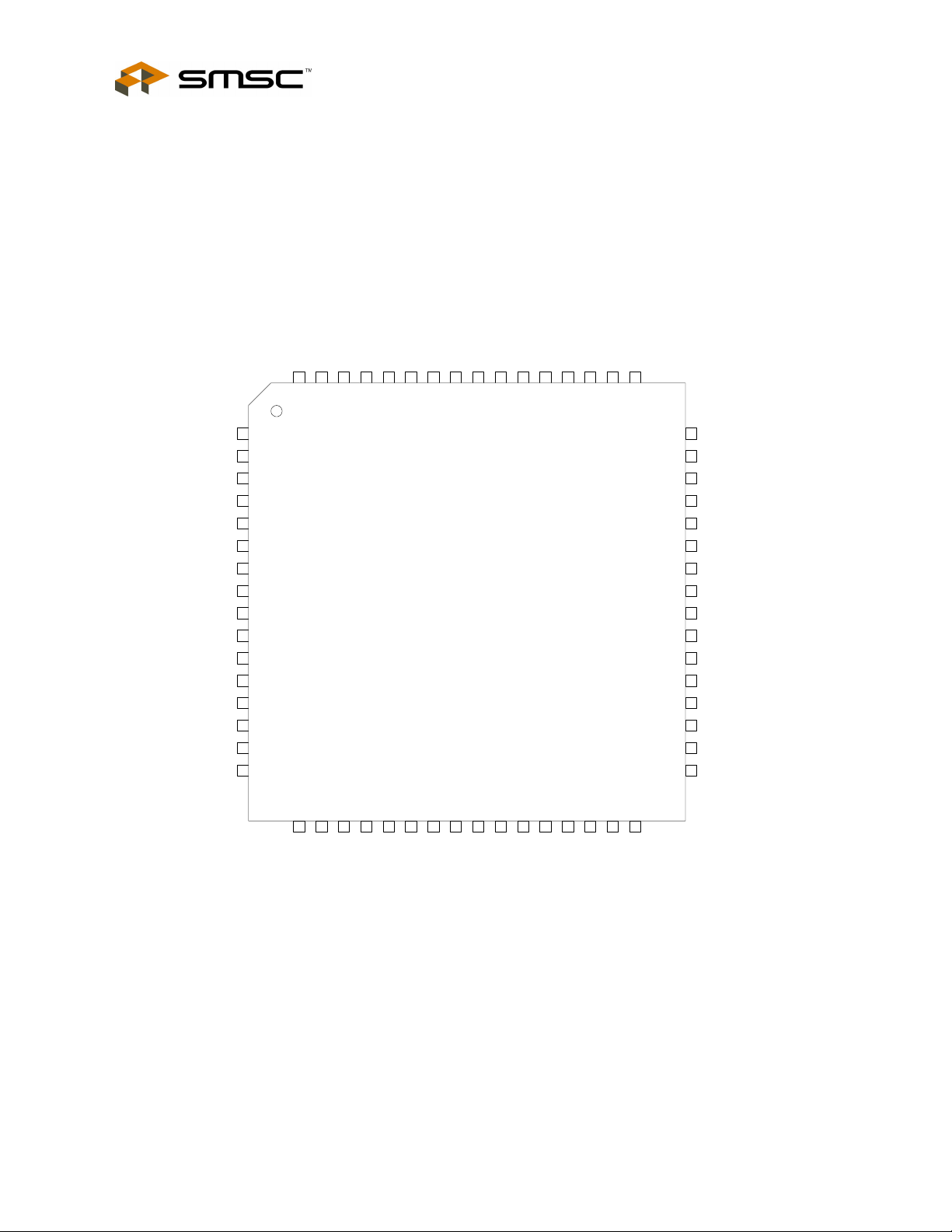
PIN # NAME PIN # NAME PIN # NAME PIN # NAME
1 nRTS1 17 PCI_RESET# 33 GP11/SYSOPT 49 PD4
2 nCTS1 18 LPCPD# 34 GP12/IO_SMI# 50 PD5
3 nDTR1 19 CLKRUN# 35 GP13/IRQIN1 51 PD6
4 nRI1 20 PCI_CLK 36 GP14/IRQIN2 52
5 nDCD1 21 SER_IRQ 37 IRRX2 53 PD7
6 IO_PME# 22
7
8
9 CLOCKI 25 GP42 41 nINIT 57 BUSY
10 LAD0 26
11
12 LAD1 28 GP44 44 PD0 60 nALF
13 LAD2 29 GP45 45
14 LAD3 30 GP46 46 PD1 62 RXD1
15 LFRAME# 31 GP47 47 PD2 63 TXD1
16 LDRQ# 32 GP10 48 PD3 64 nDSR1
VTR
VSS
VCC
23 GP40 39 IRMODE/IRRX3 55 SLCT
24 GP41 40 GP23 56 PE
27 GP43 43
VSS
VCC
38 IRTX2 54
42 nSLCTIN 58 nACK
VSS
VCC
59 nERROR
61 nSTROBE
VSS
VCC
Revision 0.2 (06-10-03) Page 10 SMSC LPC47N217
DATASHEET
Chapter 3 Pin Configuration
nDSR1
TXD1
RXD1
nSTROBE
nALF
nERROR
nACK
BUSY
PE
SLCT
64-Pin Super I/O with LPC Interface
Datasheet
VCC
PD7
VSS
PD6
PD5
PD4
nRTS1
nCTS1
nDTR1
nRI1
nDCD1
IO_PME#
VTR
VSS
CLOCKI
LAD0
VCC
LAD1
LAD2
LAD3
LFRAME#
LDRQ#
646362616059585756555453525150
1
2
3
4
5
6
7
8
9
10
11
12
13
14
15
16
171819202122232425262728293031
LPC47N217
64 PIN STQFP
49
32
48
47
46
45
44
43
42
41
40
39
38
37
36
35
34
33
PD3
PD2
PD1
VCC
PD0
VSS
nSLCTIN
nINIT
GP23
IRMODE/IRRX3
IRTX2
IRRX2
GP14/IRQIN2
GP13/IRQIN1
GP12/IO_SMI#
GP11/SYSOPT
VSS
GP40
LPCPD#
PCI_CLK
SER_IRQ
CLKRUN#
PCI_RESET#
Figure 3.1 - LPC47N217 Pin Configuration
SMSC LPC47N217 Page 11 Revision 0.2 (06-10-03)
GP41
VCC
GP42
GP43
GP44
GP45
GP46
GP47
GP10
DATASHEET
64-Pin Super I/O with LPC Interface
Datasheet
Chapter 4 Pin Description
BUFFER
PIN # NAME SYMBOL
14:12,
LPC Address/
10
Data bus 3-0
15 LPC Frame LFRAME# PCI_I Active low signal indicates start of new cycle and
16 LPC
DMA/Bus Master
Request
17 PCI RESET PCI_RESET# PCI_I Active low signal used as LPC Interface Reset.
18 LPC Power
Down
(Note 4.3)
19 PCI Clock
Controller
20 PCI Clock PCI_CLK PCI_CLK PCI clock input.
21 Serial IRQ SER_IRQ PCI_IO Serial IRQ pin used with the PCI_CLK pin to transfer
6 Power Mgt.
Event
62 Receive Data 1 RXD1 IS Receiver serial data input for port 1.
63 Transmit
Data 1
64 Data Set
Ready 1
LAD[3:0] PCI_IO Active high LPC signals used for multiplexed
LDRQ# PCI_O Active low signal used for encoded DMA/Bus Master
LPCPD# PCI_I Active low Power Down signal indicates that the
CLKRUN# PCI_OD This signal is used to indicate the PCI clock status
IO_PME# (O12/OD12) This active low Power Management Event signal
TXD1 O12 Transmit serial data output for port 1.
nDSR1 I Active low Data Set Ready inputs for the serial port.
TYPE PER
FUNCTION
(NOTE 4.1)
LPC INTERFACE (12)
command, address and data bus.
termination of broken cycle.
request for the LPC interface.
LPC47N217 should prepare for power to be shut on
the LPC interface.
and to request that a stopped clock be started.
LPC47N217 interrupts to the host.
allows the LPC47N217 to request wakeup.
SERIAL PORTS INTERFACE (8)
Handshake signal which notifies the UART that the
modem is ready to establish the communication link.
The CPU can monitor the status of nDSR signal by
reading bit 5 of Modem Status Register (MSR). A
nDSR signal state change from low to high after the
last MSR read will set MSR bit 1 to a 1. If bit 3 of
Interrupt Enable Register is set, the interrupt is
generated when nDSR changes state.
DESCRIPTION
Note: Bit 5 of MSR is the complement of nDSR.
1 Request to Send 1 nRTS1 O6 Active low Request to Send outputs for the Serial Port.
Handshake output signal notifies modem that the
UART is ready to transmit data. This signal can be
programmed by writing to bit 1 of the Modem Control
Register (MCR). The hardware reset will reset the
nRTS signal to inactive mode (high). nRTS is forced
inactive during loop mode operation.
Revision 0.2 (06-10-03) Page 12 SMSC LPC47N217
DATASHEET
PIN # NAME SYMBOL
2 Clear to
nCTS1 I Active low Clear to Send inputs for the serial port.
Send 1
BUFFER
TYPE PER
FUNCTION
(NOTE 4.1)
64-Pin Super I/O with LPC Interface
Datasheet
DESCRIPTION
Handshake signal which notifies the UART that the
modem is ready to receive data. The CPU can
monitor the status of nCTS signal by reading bit 4 of
Modem Status Register (MSR). A nCTS signal state
change from low to high after the last MSR read will
set MSR bit 0 to a 1. If bit 3 of the Interrupt Enable
Register is set, the interrupt is generated when nCTS
changes state. The nCTS signal has no effect on the
transmitter.
Note: Bit 4 of MSR is the complement of nCTS.
3 Data Terminal
Ready 1
4 Ring
Indicator 1
5 Data Carrier
Detect 1
nDTR1 O6 Active low Data Terminal Ready outputs for the serial
port. Handshake output signal notifies modem that
the UART is ready to establish data communication
link. This signal can be programmed by writing to bit 0
of Modem Control Register (MCR). The hardware
reset will reset the nDTR signal to inactive mode
(high). nDTR is forced inactive during loop mode
operation.
nRI1 I
Active low Ring Indicator inputs for the serial port.
Handshake signal which notifies the UART that the
telephone ring signal is detected by the modem. The
CPU can monitor the status of nRI signal by reading
bit 6 of Modem Status Register (MSR). A nRI signal
state change from low to high after the last MSR read
will set MSR bit 2 to a 1. If bit 3 of Interrupt Enable
Register is set, the interrupt is generated when nRI
changes state.
Note: Bit 6 of MSR is the complement of nRI.
nDCD1 I Active low Data Carrier Detect inputs for the serial
port. Handshake signal which notifies the UART that
carrier signal is detected by the modem. The CPU
can monitor the status of nDCD signal by reading bit 7
of Modem Status Register (MSR). A nDCD signal
state change from low to high after the last MSR read
will set MSR bit 3 to a 1. If bit 3 of Interrupt Enable
Register is set, the interrupt is generated when nDCD
changes state.
Note: Bit 7 of MSR is the complement of nDCD.
INFRARED INTERFACE (3)
37 IR Receive IRRX2
(Note 4.6)
38 IR Transmit IRTX2
(Note 4.6)
39 IR Mode/
IR Receive 3
SMSC LPC47N217 Page 13 Revision 0.2 (06-10-03)
IRMODE/
IRRX3
IS IR Receive.
O12 IR Transmit.
O6/
IS
IR mode.
IR Receive 3.
DATASHEET
64-Pin Super I/O with LPC Interface
Datasheet
BUFFER
PIN # NAME SYMBOL
TYPE PER
FUNCTION
(NOTE 4.1)
DESCRIPTION
PARALLEL PORT INTERFACE (17)
41 Initiate Output
(Note 4.4)
nINIT (OD14/OP14)
This output is bit 2 of the printer control register. This
is used to initiate the printer when low.
Refer to Parallel Port description for use of this pin in
ECP and EPP mode.
42 Printer Select
Input
(Note 4.4)
nSLCTIN (OD14/OP14) This active low output selects the printer. This is the
complement of bit 3 of the Printer Control Register.
Refer to Parallel Port description for use of this pin in
ECP and EPP mode.
44 Port Data 0 PD0 IOP14 Port Data 0
46 Port Data 1 PD1 IOP14 Port Data 1
47 Port Data 2 PD2 IOP14 Port Data 2
48 Port Data 3 PD3 IOP14 Port Data 3
49 Port Data 4 PD4 IOP14 Port Data 4
50 Port Data 5 PD5 IOP14 Port Data 5
51 Port Data 6 PD6 IOP14 Port Data 6
53 Port Data 7 PD7 IOP14 Port Data 7
55 Printer Selected
Status
SLCT I This high active output from the printer indicates that it
has power on. Bit 4 of the Printer Status Register
reads the SLCT input.
Refer to Parallel Port description for use of this pin in
ECP and EPP mode.
56 Paper End PE I Another status output from the printer, a high
indicating that the printer is out of paper. Bit 5 of the
Printer Status Register reads the PE input.
Refer to Parallel Port description for use of this pin in
ECP and EPP mode.
57 Busy BUSY I This is a status output from the printer, a high
indicating that the printer is not ready to receive new
data. Bit 7 of the Printer Status Register is the
complement of the BUSY input.
Refer to Parallel Port description for use of this pin in
ECP and EPP mode.
58 Acknowledge nACK I A low active output from the printer indicating that it
has received the data and is ready to accept new
data. Bit 6 of the Printer Status Register reads the
nACK input.
Refer to Parallel Port description for use of this pin in
ECP and EPP mode.
59 Error nERROR I A low on this input from the printer indicates that there
is a error condition at the printer. Bit 3 of the Printer
Status register reads the nERR input.
Refer to Parallel Port description for use of this pin in
ECP and EPP mode.
Revision 0.2 (06-10-03) Page 14 SMSC LPC47N217
DATASHEET
BUFFER
PIN # NAME SYMBOL
60 Autofeed Output
(Note 4.4)
nALF (OD14/OP14) This output goes low to cause the printer to
TYPE PER
FUNCTION
(NOTE 4.1)
automatically feed one line after each line is printed.
DESCRIPTION
The nALF output is the complement of bit 1 of the
Printer Control Register.
Refer to Parallel Port description for use of this pin in
ECP and EPP mode.
61 Strobe Output
(Note 4.4)
nSTROBE (OD14/OP14) An active low pulse on this output is used to strobe the
printer data into the printer. The nSTROBE output is
the complement of bit 0 of the Printer Control
Register.
Refer to Parallel Port description for use of this pin in
ECP and EPP mode.
GENERAL PURPOSE I/O (14)
23-25,
27-31,
General Purpose
I/O
GP40-GP47
GP10
(I/O8/OD8) Dedicated General Purpose Input/Output.
32
33 General Purpose
I/O
(System Option)
(Note 4.5)
GP11/
(SYSOPT)
(I/O8/OD8) General Purpose Input/Output.
At the trailing edge of hardware reset the GP11 pin is
latched to determine the configuration base address: 0
= Index Base I/O Address 02E Hex; 1 = Index Base
I/O Address 04E Hex.
34 General Purpose
I/O/
System Mgt.
GP12/
IO_SMI#
(I/O12/OD12)/
(O12/OD12)
General Purpose Input/Output.
Active low System Management Interrupt Output.
Interrupt
35 General Purpose
I/O/ IRQ Input 1
GP13/
IRQIN1
(I/O8/OD8)/
I
General Purpose Input/Output.
External Interrupt Input. Steerable onto one of the 15
Serial IRQs.
36 General Purpose
I/O/ IRQ Input 2
GP14/
IRQIN2
(I/O8/OD8)/
I
General Purpose Input/Output.
External Interrupt Input. Steerable onto one of the 15
Serial IRQs.
40 General Purpose
GP23 (I/O8/OD8) General Purpose Input/Output.
I/O
CLOCK PINS (1)
9 14MHz Clock CLOCKI IS 14.318MHz Clock Input.
POWER PINS (9)
11, 26,
VCC VCC +3.3 Volt Supply Voltage.
45, 54
7 VTR VTR +3.3 Volt Standby Voltage.
8, 22,
VSS VSS Ground.
43, 52
64-Pin Super I/O with LPC Interface
Datasheet
Note 4.1 The "n" as the first letter of a signal name or the “#” as the suffix of a signal name indicates an “Active Low”
signal.
SMSC LPC47N217 Page 15 Revision 0.2 (06-10-03)
DATASHEET

64-Pin Super I/O with LPC Interface
Datasheet
Note 4.2 Buffer types per function on multiplexed pins are separated by a slash “/”. Buffer types in parenthesis
represent multiple buffer types for a single pin function.
Note 4.3 The LPCPD# pin may be tied high.
Note 4.4 Active (push-pull) output drivers are required on these pins in the enhanced parallel port modes.
Note 4.5 The GP11/SYSOPT pin requires an external pulldown resistor to put the base IO address for configuration
at 0x02E. An external pullup resistor is required to move the base IO address for configuration to 0x04E.
Note 4.6 To activate the IRTX2 and IRRX2 pins set bits[7:6] IR Output Mux located in CR0A to ‘01’.
4.1 Buffer Type Description
I Input TTL Compatible.
IS Input with Schmitt Trigger.
O6 Output, 6mA sink, 3mA source.
O8 Output, 8mA sink, 4mA source.
OD8 Open Drain Output, 8mA sink.
IO8 Input/Output, 8mA sink, 4mA source.
O12 Output, 12mA sink, 6mA source.
OD12 Open Drain Output, 12mA sink.
IO12 Input/Output, 12mA sink, 6mA source.
OD14 Open Drain Output, 14mA sink.
OP14 Output, 14mA sink, 14mA source.
IOP14 Input/Output, 14mA sink, 14mA source. Backdrive protected.
PCI_I Input. These pins meet the PCI 3.3V AC and DC Characteristics.
PCI_O Output. These pins meet the PCI 3.3V AC and DC Characteristics. (Note 4.7)
PCI_OD Open Drain Output. These pins meet the PCI 3.3V AC and DC Characteristics.
PCI_IO Input/Output. These pins meet the PCI 3.3V AC and DC Characteristics.
PCI_ICLK Clock Input. These pins meet the PCI 3.3V AC and DC Characteristics and timing.
Note 4.7 See the PCI Local Bus Specification, Revision 2.1, Section 4.2.2.
(Note 4.7)
(Note 4.7)
(Note 4.7)
(Note 4.8)
Note 4.8 See the PCI Local Bus Specification, Revision 2.1, Section 4.2.2. and 4.2.3.
Revision 0.2 (06-10-03) Page 16 SMSC LPC47N217
DATASHEET

Chapter 5 Block Diagram
64-Pin Super I/O with LPC Interface
Datasheet
SER_IRQ
PCI_CLK
LAD0
LAD1
LAD2
LAD3
LFRAME#
LDRQ#
PCI_RESET#
LPCPD#
CLKRUN#
V
TR
Vcc
INTERFACE
Vss
SERIAL
IRQ
LPC BUS
IO_SMI#*
CLOCK
GEN
CLOCKI
IO_PME#
SMI PME WDT
CONTROL, ADDRESS, DATA
CONFIGURATION
REGISTERS
BLOCK
Figure 5.1 - LPC47N217 Block Diagram
ACPI
MULTI-MODE
PARALLEL
PORT
GENERAL
PURPOSE
I/O
16C550
COMPATIBLE
SERIAL
PORT 1
INFRARED
INTERFACE
PD[0:7],
BUSY, SLCT,
PE, nERROR, nACK
nSLCTIN, nALF
nINIT, nSTROBE
GP10, GP11,
GP12*, GP13*,
GP14*,
GP23*,
GP4[0:7]
IRQIN1*, IRQIN2*
TXD1, nRTS1, nDTR1
nCTS1, RXD1,
nDSR1, nDCD1, nRI1
IRTX2, IRMODE*
IRRX2, IRRX3*
*
Denotes Multifunction Pins
SMSC LPC47N217 Page 17 Revision 0.2 (06-10-03)
DATASHEET

64-Pin Super I/O with LPC Interface
Datasheet
Chapter 6 3.3 Volt Operation / 5 Volt Tolerance
The LPC47N217 is a 3.3 Volt part. It is intended solely for 3.3V applications. Non-LPC bus pins are 5V
tolerant; that is, the input voltage is 5.5V max, and the I/O buffer output pads are backdrive protected.
The LPC interface pins are 3.3 V only. These signals meet PCI DC specifications for 3.3V signaling.
These pins are:
LAD[3:0]
LFRAME#
LDRQ#
LPCPD#
The input voltage for all other pins is 5.5V max. These pins include all non-LPC Bus pins and the following
pins:
PCI_RESET#
PCI_CLK
SER_IRQ
CLKRUN#
IO_PME#
Revision 0.2 (06-10-03) Page 18 SMSC LPC47N217
DATASHEET

Chapter 7 Power Functionality
The LPC47N217 has two power planes: VCC and VTR.
7.1 VCC Power
The LPC47N217 is a 3.3 Volt part. The VCC supply is 3.3 Volts (nominal). See Chapter 20 - Operational
Description and the Maximum Current Values subsection.
7.2 VTR Support
The LPC47N217 requires a trickle supply (VTR) to provide sleep current for the programmable wake-up
events in the PME interface when VCC is removed. The VTR supply is 3.3 Volts (nominal). See the
Operational Description section. The maximum VTR current that is required depends on the functions that
are used in the part. See Trickle Power Functionality subsection and the Maximum Current Values
subsection. If the LPC47N217 is not intended to provide wake-up capabilities on standby current, VTR can
be connected to VCC. The VTR pin generates a VTR Power-on-Reset signal to initialize these
components.
64-Pin Super I/O with LPC Interface
Datasheet
Note: If VTR is to be used for programmable wake-up events when VCC is removed, VTR must be at its full
minimum potential at least 10 µs before VCC begins a power-on cycle.
7.3 Internal PWRGOOD
An internal PWRGOOD logical control is included to minimize the effects of pin-state uncertainty in the
host interface as VCC cycles on and off. When the internal PWRGOOD signal is “1” (active), VCC > 2.3V
(nominal), and the LPC47N217 host interface is active. When the internal PWRGOOD signal is “0”
(inactive), VCC ≤ 2.3V (nominal), and the LPC47N217 host interface is inactive; that is, LPC bus reads and
writes will not be decoded.
The LPC47N217 device pins IO_PME#, nRI1, and most GPIOs (as input) are part of the PME interface
and remain active when the internal PWRGOOD signal has gone inactive, provided VTR is powered. See
Section 7.4 - Trickle Power Functionality.
7.4 Trickle Power Functionality
When the LPC47N217 is running under VTR only, the PME wakeup events are active and (if enabled) able
to assert the IO_PME# pin active low. The following lists the wakeup events:
UART 1 Ring Indicator
GPIOs for wakeup. See below.
The following requirements apply to all I/O pins that are specified to be 5 volt tolerant.
I/O buffers that are wake-up event compatible are powered by VCC. Under VTR power (VCC=0),
these pins may only be configured as inputs. These pins have input buffers into the wakeup logic that
are powered by VTR.
I/O buffers that may be configured as either push-pull or open drain under VTR power (VCC=0), are
powered by VTR. This means they will, at a minimum, source their specified current from VTR even
when VCC is present.
SMSC LPC47N217 Page 19 Revision 0.2 (06-10-03)
DATASHEET

64-Pin Super I/O with LPC Interface
Datasheet
The GPIOs that are used for PME wakeup inputs are GP10-GP14, GP23. These GPIOs function as
follows:
Buffers are powered by VCC, but in the absence of VCC they are backdrive protected (they do not
impose a load on any external VTR powered circuitry). They are wakeup compatible as inputs under
VTR power. These pins have input buffers into the wakeup logic that are powered by VTR.
All GPIOs listed above are for PME wakeup as a GPIO function (or alternate function).
See the Table in the GPIO section for more information.
The following list summarizes the blocks, registers and pins that are powered by VTR.
PME interface block
Runtime register block (includes all PME, SMI, GP data registers)
Pins for PME Wakeup:
− GPIOs (GP10-GP14, GP23)
− IO_PME#
− nRI1
7.5 Maximum Current Values
See Chapter 20 - Operational Description for the maximum current values.
The maximum VTR current, I
(i.e., 0V or 3.3V). The total maximum current for the part is the unloaded value PLUS the maximum
current sourced by the pin that is driven by VTR. The pin that is powered by VTR (as output) is IO_PME#.
This pin, if configured as a push-pull output, will source a minimum of 6mA at 2.4V when driving.
The maximum VCC current, I
(i.e., 0V or 3.3V).
, is given with all outputs open (not loaded), and all inputs in a fixed state
TR
, is given with all outputs open (not loaded), and all inputs in a fixed state
CC
7.6 Power Management Events (PME/SCI)
The LPC47N217 offers support for Power Management Events (PMEs), also referred to as System Control
Interrupt (SCI) events. The terms PME and SCI are used synonymously throughout this document to refer
to the indication of an event to the chipset via the assertion of the IO_PME# pin. See PME Support Chapter 17.
Revision 0.2 (06-10-03) Page 20 SMSC LPC47N217
DATASHEET
Chapter 8 Functional Description
8.1 Super I/O Registers
The address map, shown below in Table 8.1, shows the addresses of the different blocks of the Super I/O
immediately after power up. The base addresses of the serial and parallel ports, runtime register block,
and configuration register block can be moved via the configuration registers. Some addresses are used to
access more than one register.
8.2 Host Processor Interface (LPC)
The host processor communicates with the LPC47N217 through a series of read/write registers via the
LPC interface. The port addresses for these registers are shown in Table 8.1. Register access is
accomplished through I/O cycles or DMA transfers. All registers are 8 bits wide.
Table 8.1 - Super I/O Block Addresses
ADDRESS BLOCK NAME NOTES
Base+(0-7) Serial Port Com 1
Base1+(0-7)
Base2+(0-7)
Base+(0-3)
Base+(0-7)
Base+(0-3), +(400-402)
Base+(0-7), +(400-402)
Base + (0-F) Runtime Registers
Base + (0-1) Configuration
Serial Port Com 2
Parallel Port
SPP
EPP
ECP
ECP+EPP+SPP
IR Support
FIR and CIR
64-Pin Super I/O with LPC Interface
Datasheet
Note 1: Refer to the configuration register descriptions for setting the base address.
8.3 LPC Interface
The following sub-sections specify the implementation of the LPC bus.
8.3.1 LPC Interface Signal Definition
The signals required for the LPC bus interface are described in the table below. LPC bus signals use PCI
33MHz electrical signal characteristics.
SIGNAL
NAME
LAD[3:0] I/O LPC address/data bus. Multiplexed command, address and data bus.
LFRAME# Input Frame signal. Indicates start of new cycle and termination of broken cycle
PCI_RESET# Input PCI Reset. Used as LPC Interface Reset.
LDRQ# Output Encoded DMA/Bus Master request for the LPC interface.
SMSC LPC47N217 Page 21 Revision 0.2 (06-10-03)
TYPE DESCRIPTION
DATASHEET
64-Pin Super I/O with LPC Interface
Datasheet
SIGNAL
NAME
IO_PME# OD Power Mgt Event signal. Allows the LPC47N217 to request wakeup.
LPCPD# Input Powerdown Signal. Indicates that the LPC47N217 should prepare for power to be
SER_IRQ I/O Serial IRQ.
PCI_CLK Input PCI Clock.
CLKRUN# I/OD Clock Run. Allows the LPC47N217 to request the stopped PCI_CLK be started.
TYPE DESCRIPTION
shut on the LPC interface.
8.3.1.1 LPC Cycles
The following cycle types are supported by the LPC protocol.
Cycle Type Transfer Size
I/O Write 1 Byte
I/O Read 1 Byte
DMA Write 1 Byte
DMA Read 1 Byte
The LPC47N217 ignores cycles that it does not support.
8.3.1.2 Field Definitions
The data transfers are based on specific fields that are used in various combinations, depending on the
cycle type. These fields are driven onto the LAD[3:0] signal lines to communicate address, control and
data information over the LPC bus between the host and the LPC47N217. See the Low Pin Count (LPC)
Interface Specification Revision 1.0 from Intel, Section 4.2 for definition of these fields.
8.3.1.3 LFRAME# Usage
LFRAME# is used by the host to indicate the start of cycles and the termination of cycles due to an abort
or time-out condition. This signal is to be used by the LPC47N217 to know when to monitor the bus for a
cycle.
This signal is used as a general notification that the LAD[3:0] lines contain information relative to the start
or stop of a cycle, and that the LPC47N217 monitors the bus to determine whether the cycle is intended for
it. The use of LFRAME# allows the LPC47N217 to enter a lower power state internally. There is no need
for the LPC47N217 to monitor the bus when it is inactive, so it can decouple its state machines from the
bus, and internally gate its clocks.
When the LPC47N217 samples LFRAME# active, it immediately stops driving the LAD[3:0] signal lines on
the next clock and monitor the bus for new cycle information.
The LFRAME# signal functions as described in the Low Pin Count (LPC) Interface Specification Revision
1.0.
8.3.1.4 I/O Read and Write Cycles
The LPC47N217 is the target for I/O cycles. I/O cycles are initiated by the host for register or FIFO
accesses, and will generally have minimal Sync times. The minimum number of wait-states between bytes
is 1. EPP cycles will depend on the speed of the external device, and may have much longer Sync times.
Data transfers are assumed to be exactly 1-byte. If the CPU requested a 16 or 32-bit transfer, the host will
break it up into 8-bit transfers.
Revision 0.2 (06-10-03) Page 22 SMSC LPC47N217
DATASHEET

See the Low Pin Count (LPC) Interface Specification Reference, Section 5.2, for the sequence of cycles
for the I/O Read and Write cycles.
8.3.1.5 DMA Read and Write Cycles
DMA read cycles involve the transfer of data from the host (main memory) to the LPC47N217. DMA write
cycles involve the transfer of data from the LPC47N217 to the host (main memory). Data will be coming
from or going to a FIFO and will have minimal Sync times. Data transfers to/from the LPC47N217 are 1
byte.
See the Low Pin Count (LPC) Interface Specification Reference, Section 6.4, for the field definitions and
the sequence of the DMA Read and Write cycles.
8.3.1.6 DMA Protocol
DMA on the LPC bus is handled through the use of the LDRQ# lines from the LPC47N217 and special
encodings on LAD[3:0] from the host.
The DMA mechanism for the LPC bus is described in the Low Pin Count (LPC) Specification Revision 1.0.
64-Pin Super I/O with LPC Interface
Datasheet
8.3.2 Power Management
8.3.2.1 CLOCKRUN Protocol
See the Low Pin Count (LPC) Interface Specification Reference, Section 8.1.
8.3.2.2 LPCPD Protocol
The LPC47N217 will function properly if the LPCPD# signal goes active and then inactive again without
PCI_RESET# becoming active. This is a requirement for notebook power management functions.
Although the LPC Bus spec 1.0 section 8.2 states, "After LPCPD# goes back inactive, the LPC I/F will
always be reset using LRST#”, this statement does not apply for mobile systems. LRST# (PCI_RESET#)
will not occur if the LPC Bus power was not removed. For example, when exiting a "light" sleep state
(ACPI S1, APM POS), LRST# (PCI_RESET#) will not occur. When exiting a "deeper" sleep state (ACPI
S3-S5, APM STR, STD, soft-off), LRST# (PCI_RESET#) will occur.
The LPCPD# pin is implemented as a “local” powergood for the LPC bus in the LPC47N217. It is not used
as a global powergood for the chip. It is used to reset the LPC block and hold it in reset.
An internal powergood is implemented in LPC47N217 to minimize power dissipation in the entire chip.
Prior to going to a low-power state, the system will assert the LPCPD# signal. It will go active at least 30
microseconds prior to the LCLK# (PCI_CLK) signal stopping low and power being shut to the other LPC I/F
signals.
Upon recognizing LPCPD# active, the LPC47N217 will drive the LDRQ# signal low or tri-state, and do so
until LPCPD# goes back active.
Upon recognizing LPCPD# inactive, the LPC47N217 will drive its LDRQ# signal high.
See the Low Pin Count (LPC) Interface Specification Reference, Section 8.2.
SMSC LPC47N217 Page 23 Revision 0.2 (06-10-03)
DATASHEET

64-Pin Super I/O with LPC Interface
Datasheet
8.3.2.3 SYNC Protocol
See the Low Pin Count (LPC) Interface Specification Reference, Section 4.2.1.8 for a table of valid SYNC
values.
8.3.2.4 Typical Usage
The SYNC pattern is used to add wait states. For read cycles, the LPC47N217 immediately drives the
SYNC pattern upon recognizing the cycle. The host immediately drives the sync pattern for write cycles. If
the LPC47N217 needs to assert wait states, it does so by driving 0101 or 0110 on LAD[3:0] until it is ready,
at which point it will drive 0000 or 1001. The LPC47N217 will choose to assert 0101 or 0110, but not
switch between the two patterns.
The data (or wait state SYNC) will immediately follow the 0000 or 1001 value.
The SYNC value of 0101 is intended to be used for normal wait states, wherein the cycle will complete
within a few clocks. The LPC47N217 uses a SYNC of 0101 for all wait states in a DMA transfer.
The SYNC value of 0110 is intended to be used where the number of wait states is large. This is provided
for EPP cycles, where the number of wait states could be quite large (>1 microsecond). However, the
LPC47N217 uses a SYNC of 0110 for all wait states in an I/O transfer.
The SYNC value is driven within 3 clocks.
8.3.2.5 SYNC Timeout
The SYNC value is driven within 3 clocks. If the host observes 3 consecutive clocks without a valid SYNC
pattern, it will abort the cycle.
The LPC47N217 does not assume any particular timeout. When the host is driving SYNC, it may have to
insert a very large number of wait states, depending on PCI latencies and retries.
8.3.2.6 SYNC Patterns and Maximum Number of SYNCS
If the SYNC pattern is 0101, then the host assumes that the maximum number of SYNCs is 8.
If the SYNC pattern is 0110, then no maximum number of SYNCs is assumed. The LPC47N217 has
protection mechanisms to complete the cycle. This is used for EPP data transfers and will utilize the same
timeout protection that is in EPP.
8.3.2.7 SYNC Error Indication
The LPC47N217 reports errors via the LAD[3:0] = 1010 SYNC encoding.
If the host was reading data from the LPC47N217, data will still be transferred in the next two nibbles. This
data may be invalid, but it will be transferred by the LPC47N217. If the host was writing data to the
LPC47N217, the data had already been transferred.
In the case of multiple byte cycles, such as DMA cycles, an error SYNC terminates the cycle. Therefore, if
the host is transferring 4 bytes from a device, if the device returns the error SYNC in the first byte, the
other three bytes will not be transferred.
Revision 0.2 (06-10-03) Page 24 SMSC LPC47N217
DATASHEET

8.3.2.8 I/O and DMA START Fields
I/O and DMA cycles use a START field of 0000.
8.3.2.9 Reset Policy
The following rules govern the reset policy:
1. When PCI_RESET# goes inactive (high), the clock is assumed to have been running for 100usec prior
to the removal of the reset signal, so that everything is stable. This is the same reset active time after
clock is stable that is used for the PCI bus.
2. When PCI_RESET# goes active (low):
a) the host drives the LFRAME# signal high, tristates the LAD[3:0] signals, and ignores the LDRQ#
signal.
b) the LPC47N217 ignores LFRAME#, tristate the LAD[3:0] pins and drive the LDRQ# signal
inactive (high).
8.3.3 LPC Transfers
8.3.3.1 Wait State Requirements
64-Pin Super I/O with LPC Interface
Datasheet
I/O Transfers
The LPC47N217 inserts three wait states for an I/O read and two wait states for an I/O write cycle. A
SYNC of 0110 is used for all I/O transfers. The exception to this is for transfers where IOCHRDY would be
deasserted in an ISA transfer (i.e., EPP or IrCC transfers) in which case the sync pattern of 0110 is used
and a large number of syncs may be inserted (up to 330 which corresponds to a timeout of 10us).
DMA Transfers
The LPC47N217 inserts three wait states for a DMA read and four wait states for a DMA write cycle. A
SYNC of 0101 is used for all DMA transfers.
See the example timing for the LPC cycles in Chapter 21 - Timing Diagrams.
SMSC LPC47N217 Page 25 Revision 0.2 (06-10-03)
DATASHEET

64-Pin Super I/O with LPC Interface
Datasheet
Chapter 9 Serial Port (UART)
The LPC47N217 incorporates one full function UART (UART 1), which is compatible with the 16450, the
16450 ACE registers and the 16C550A. The LPC47N217 also includes a reduced function UART (UART
2) to support the IR interface. See Chapter 10 Infrared Interface on page 42.
The UARTS perform serial-to-parallel conversion on received characters and parallel-to-serial conversion
on transmit characters. The data rates are independently programmable from 460.8K baud down to 50
baud. The character options are programmable for 1 start; 1, 1.5 or 2 stop bits; even, odd, sticky or no
parity; and prioritized interrupts. The UARTs each contain a programmable baud rate generator that is
capable of dividing the input clock or crystal by a number from 1 to 65535. The UARTs are also capable of
supporting the MIDI data rate. Refer to the Configuration Registers for information on disabling, power
down and changing the base address of the UARTs. The interrupt from a UART is enabled by
programming OUT2 of that UART to a logic "1". OUT2 being a logic "0" disables that UART's interrupt.
The second UART also supports IrDA 1.2 (4Mbps), HP-SIR, ASK-IR and Consumer IR infrared modes of
operation.
9.1 Register Description
Addressing of the accessible registers of the Serial Port is shown below. The base addresses of the serial
ports are defined by the configuration registers (see Chapter 19 - Configuration). The Serial Port registers
are located at sequentially increasing addresses above these base addresses. The LPC47N217 contains
two serial ports, each of which contain a register set as described below.
Table 9.1 - Addressing the Serial Port
DLAB
(NOTE 9.1)
0 0 0 0 Receive Buffer (read)
0 0 0 0 Transmit Buffer (write)
0 0 0 1 Interrupt Enable (read/write)
X 0 1 0 Interrupt Identification (read)
X 0 1 0 FIFO Control (write)
X 0 1 1 Line Control (read/write)
X 1 0 0 Modem Control (read/write)
X 1 0 1 Line Status (read/write)
X 1 1 0 Modem Status (read/write)
X 1 1 1 Scratchpad (read/write)
1 0 0 0 Divisor LSB (read/write)
1 0 0 1 Divisor MSB (read/write
Note 9.1 DLAB is Bit 7 of the Line Control Register
The following section describes the operation of the registers.
A2 A1 A0
REGISTER NAME
Revision 0.2 (06-10-03) Page 26 SMSC LPC47N217
DATASHEET

9.1.1 Receive Buffer Register (RB)
Address Offset = 0H, DLAB = 0, READ ONLY
This register holds the received incoming data byte. Bit 0 is the least significant bit, which is transmitted
and received first. Received data is double buffered; this uses an additional shift register to receive the
serial data stream and convert it to a parallel 8 bit word which is transferred to the Receive Buffer register.
The shift register is not accessible.
9.1.2 Transmit Buffer Register (TB)
Address Offset = 0H, DLAB = 0, WRITE ONLY
This register contains the data byte to be transmitted. The transmit buffer is double buffered, utilizing an
additional shift register (not accessible) to convert the 8 bit data word to a serial format. This shift register
is loaded from the Transmit Buffer when the transmission of the previous byte is complete.
9.1.3 Interrupt Enable Register (IER)
Address Offset = 1H, DLAB = 0, READ/WRITE
64-Pin Super I/O with LPC Interface
Datasheet
The lower four bits of this register control the enables of the five interrupt sources of the Serial Port
interrupt. It is possible to totally disable the interrupt system by resetting bits 0 through 3 of this register.
Similarly, setting the appropriate bits of this register to a high, selected interrupts can be enabled.
Disabling the interrupt system inhibits the Interrupt Identification Register and disables any Serial Port
interrupt out of the LPC47N217. All other system functions operate in their normal manner, including the
Line Status and MODEM Status Registers. The contents of the Interrupt Enable Register are described
below.
Bit 0
This bit enables the Received Data Available Interrupt (and timeout interrupts in the FIFO mode) when set
to logic "1".
Bit 1
This bit enables the Transmitter Holding Register Empty Interrupt when set to logic "1".
Bit 2
This bit enables the Received Line Status Interrupt when set to logic "1". The error sources causing the
interrupt are Overrun, Parity, Framing and Break. The Line Status Register must be read to determine the
source.
Bit 3
This bit enables the MODEM Status Interrupt when set to logic "1". This is caused when one of the
Modem Status Register bits changes state.
Bits 4 through 7
These bits are always logic "0".
SMSC LPC47N217 Page 27 Revision 0.2 (06-10-03)
DATASHEET
64-Pin Super I/O with LPC Interface
Datasheet
9.1.4 FIFO Control Register (FCR)
Address Offset = 2H, DLAB = X, WRITE
This is a write only register at the same location as the IIR. This register is used to enable and clear the
FIFOs, set the RCVR FIFO trigger level. Note: DMA is not supported. The UART1 and UART2 FCR’s are
shadowed in the UART1 FIFO Control Shadow Register (CR15) and UART2 FIFO Control Shadow
Register (CR16). See Chapter 19 - Configuration for description on these registers.
Bit 0
Setting this bit to a logic "1" enables both the XMIT and RCVR FIFOs. Clearing this bit to a logic "0"
disables both the XMIT and RCVR FIFOs and clears all bytes from both FIFOs. When changing from FIFO
Mode to non-FIFO (16450) mode, data is automatically cleared from the FIFOs. This bit must be a 1 when
other bits in this register are written to or they will not be properly programmed.
Bit 1
Setting this bit to a logic "1" clears all bytes in the RCVR FIFO and resets its counter logic to 0. The shift
register is not cleared. This bit is self-clearing.
Bit 2
Setting this bit to a logic "1" clears all bytes in the XMIT FIFO and resets its counter logic to 0. The shift
register is not cleared. This bit is self-clearing.
Bit 3
Writing to this bit has no effect on the operation of the UART. DMA modes are not supported in this chip.
Bit 4,5
Reserved
Bit 6,7
These bits are used to set the trigger level for the RCVR FIFO interrupt.
BIT 7 BIT 6
0 0 1
0 1 4
1 0 8
1 1 14
TRIGGER LEVEL (BYTES)
9.1.5 Interrupt Identification Register (IIR)
RCVR FIFO
Address Offset = 2H, DLAB = X, READ
By accessing this register, the host CPU can determine the highest priority interrupt and its source. Four
levels of priority interrupt exist. They are in descending order of priority:
1. Receiver Line Status (highest priority)
2. Received Data Ready
Revision 0.2 (06-10-03) Page 28 SMSC LPC47N217
DATASHEET
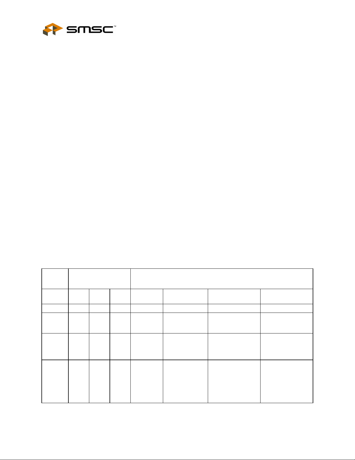
64-Pin Super I/O with LPC Interface
Datasheet
3. Transmitter Holding Register Empty
4. MODEM Status (lowest priority)
Information indicating that a prioritized interrupt is pending and the source of that interrupt is stored in the
Interrupt Identification Register (refer to Interrupt Control Table). When the CPU accesses the IIR, the
Serial Port freezes all interrupts and indicates the highest priority pending interrupt to the CPU. During this
CPU access, even if the Serial Port records new interrupts, the current indication does not change until
access is completed. The contents of the IIR are described below.
Bit 0
This bit can be used in either a hardwired prioritized or polled environment to indicate whether an interrupt
is pending. When bit 0 is a logic "0", an interrupt is pending and the contents of the IIR may be used as a
pointer to the appropriate internal service routine. When bit 0 is a logic "1", no interrupt is pending.
Bits 1 and 2
These two bits of the IIR are used to identify the highest priority interrupt pending as indicated by the
Interrupt Control Table.
Bit 3
In non-FIFO mode, this bit is a logic "0". In FIFO mode this bit is set along with bit 2 when a timeout
interrupt is pending.
Bits 4 and 5
These bits of the IIR are always logic "0".
Bits 6 and 7
These two bits are set when the FIFO CONTROL Register bit 0 equals 1.
Table 9.2 - Interrupt Control Table
FIFO
MODE
ONLY
BIT 3 BIT 2 BIT 1 BIT 0
INTERRUPT
IDENTIFICATION
REGISTER
PRIORITY
LEVEL
INTERRUPT SET AND RESET FUNCTIONS
INTERRUPT
TYPE
INTERRUPT
SOURCE
RESET CONTROL
INTERRUPT
0 0 0 1 - None None -
0 1 1 0 Highest Receiver Line
Status
Overrun Error, Parity
Error, Framing Error
Reading the Line
Status Register
or Break Interrupt
0 1 0 0 Second Received Data
Available
Receiver Data
Available
Read Receiver Buffer
or the FIFO drops
below the trigger
level.
1 1 0 0 Second Character
Timeout
Indication
No Characters Have
Been Removed From
or Input to the RCVR
Reading the
Receiver Buffer
Register
FIFO during the last
4 Char times and
there is at least 1
char in it during this
SMSC LPC47N217 Page 29 Revision 0.2 (06-10-03)
DATASHEET
64-Pin Super I/O with LPC Interface
p
Datasheet
FIFO
MODE
ONLY
BIT 3 BIT 2 BIT 1 BIT 0
0 0 1 0 Third Transmitter
0 0 0 0 Fourth MODEM Status Clear to Send or
INTERRUPT
IDENTIFICATION
REGISTER
PRIORITY
LEVEL
INTERRUPT SET AND RESET FUNCTIONS
INTERRUPT
TYPE
Holding Register
Empty
INTERRUPT
time
Transmitter Holding
Register Empty
Data Set Ready or
Ring Indicator or
Data Carrier Detect
9.1.6 Line Control Register (LCR)
Address Offset = 3H, DLAB = 0, READ/WRITE
Start LSB Data 5-8 bits MSB Parity Sto
Figure 9.1 - Serial Data
SOURCE
INTERRUPT
RESET CONTROL
Reading the IIR
Register (if Source of
Interrupt) or Writing
the Transmitter
Holding Register
Reading the MODEM
Status Register
This register contains the format information of the serial line. The bit definitions are:
Bits 0 and 1
These two bits specify the number of bits in each transmitted or received serial character. The encoding of
bits 0 and 1 is as follows:
The Start, Stop and Parity bits are not included in the word length.
BIT 1 BIT 0 WORD LENGTH
0
0
1
1
0
1
0
1
5 Bits
6 Bits
7 Bits
8 Bits
Revision 0.2 (06-10-03) Page 30 SMSC LPC47N217
DATASHEET

64-Pin Super I/O with LPC Interface
Bit 2
This bit specifies the number of stop bits in each transmitted or received serial character. The following
table summarizes the information.
BIT 2
WORD LENGTH
NUMBER OF
STOP BITS
0 -- 1
1 5 bits 1.5
1 6 bits 2
1 7 bits 2
1 8 bits 2
Note: The receiver will ignore all stop bits beyond the first, regardless of the number used in transmitting.
Bit 3
Parity Enable bit. When bit 3 is a logic "1", a parity bit is generated (transmit data) or checked (receive
data) between the last data word bit and the first stop bit of the serial data. (The parity bit is used to
generate an even or odd number of 1s when the data word bits and the parity bit are summed).
Datasheet
Bit 4
Even Parity Select bit. When bit 3 is a logic "1" and bit 4 is a logic "0", an odd number of logic "1"'s is
transmitted or checked in the data word bits and the parity bit. When bit 3 is a logic "1" and bit 4 is a logic
"1" an even number of bits is transmitted and checked.
Bit 5
Stick Parity bit. When parity is enabled it is used in conjunction with bit 4 to select Mark or Space Parity.
When LCR bits 3, 4 and 5 are 1 the Parity bit is transmitted and checked as 0 (Space Parity). If bits 3 and
5 are 1 and bit 4 is a 0, then the Parity bit is transmitted and checked as 1 (Mark Parity). If bit 5 is 0 Stick
Parity is disabled.
Bit 6
Set Break Control bit. When bit 6 is a logic "1", the transmit data output (TXD) is forced to the Spacing or
logic "0" state and remains there (until reset by a low level bit 6) regardless of other transmitter activity.
This feature enables the Serial Port to alert a terminal in a communications system.
Bit 7
Divisor Latch Access bit (DLAB). It must be set high (logic "1") to access the Divisor Latches of the Baud
Rate Generator during read or write operations. It must be set low (logic "0") to access the Receiver Buffer
Register, the Transmitter Holding Register, or the Interrupt Enable Register.
SMSC LPC47N217 Page 31 Revision 0.2 (06-10-03)
DATASHEET

64-Pin Super I/O with LPC Interface
Datasheet
9.1.7 Modem Control Register (MCR)
Address Offset = 4H, DLAB = X, READ/WRITE
This 8 bit register controls the interface with the MODEM or data set (or device emulating a MODEM). The
contents of the MODEM control register are described below.
Bit 0
This bit controls the Data Terminal Ready (nDTR) output. When bit 0 is set to a logic "1", the nDTR output is
forced to a logic "0". When bit 0 is a logic "0", the nDTR output is forced to a logic "1".
Bit 1
This bit controls the Request To Send (nRTS) output. Bit 1 affects the nRTS output in a manner identical to
that described above for bit 0.
Bit 2
This bit controls the Output 1 (OUT1) bit. This bit does not have an output pin and can only be read or
written by the CPU.
Bit 3
Output 2 (OUT2). This bit is used to enable an UART interrupt. When OUT2 is a logic "0", the serial port
interrupt output is forced to a high impedance state - disabled. When OUT2 is a logic "1", the serial port
interrupt outputs are enabled.
Bit 4
This bit provides the loopback feature for diagnostic testing of the Serial Port. When bit 4 is set to logic
"1", the following occur:
1. The TXD is set to the Marking State(logic "1").
2. The receiver Serial Input (RXD) is disconnected.
3. The output of the Transmitter Shift Register is "looped back" into the Receiver Shift Register input.
4. All MODEM Control inputs (nCTS, nDSR, nRI and nDCD) are disconnected.
5. The four MODEM Control outputs (nDTR, nRTS, OUT1 and OUT2) are internally connected to the
four MODEM Control inputs (nDSR, nCTS, RI, DCD).
6. The Modem Control output pins are forced inactive high.
7. Data that is transmitted is immediately received.
This feature allows the processor to verify the transmit and receive data paths of the Serial Port. In the
diagnostic mode, the receiver and the transmitter interrupts are fully operational. The MODEM Control
Interrupts are also operational but the interrupts' sources are now the lower four bits of the MODEM
Control Register instead of the MODEM Control inputs. The interrupts are still controlled by the Interrupt
Enable Register.
Bits 5 through 7
These bits are permanently set to logic zero.
Revision 0.2 (06-10-03) Page 32 SMSC LPC47N217
DATASHEET

9.1.8 Line Status Register (LSR)
Address Offset = 5H, DLAB = X, READ/WRITE
Bit 0
Data Ready (DR). It is set to a logic "1" whenever a complete incoming character has been received and
transferred into the Receiver Buffer Register or the FIFO. Bit 0 is reset to a logic "0" by reading all of the data
in the Receive Buffer Register or the FIFO.
Bit 1
Overrun Error (OE). Bit 1 indicates that data in the Receiver Buffer Register was not read before the next
character was transferred into the register, thereby destroying the previous character. In FIFO mode, an
overrunn error will occur only when the FIFO is full and the next character has been completely received in the
shift register, the character in the shift register is overwritten but not transferred to the FIFO. The OE indicator
is set to a logic "1" immediately upon detection of an overrun condition, and reset whenever the Line Status
Register is read.
Bit 2
Parity Error (PE). Bit 2 indicates that the received data character does not have the correct even or odd
parity, as selected by the even parity select bit. The PE is set to a logic "1" upon detection of a parity error
and is reset to a logic "0" whenever the Line Status Register is read. In the FIFO mode this error is
associated with the particular character in the FIFO it applies to. This error is indicated when the
associated character is at the top of the FIFO.
64-Pin Super I/O with LPC Interface
Datasheet
Bit 3
Framing Error (FE). Bit 3 indicates that the received character did not have a valid stop bit. Bit 3 is set to
a logic "1" whenever the stop bit following the last data bit or parity bit is detected as a zero bit (Spacing
level). The FE is reset to a logic "0" whenever the Line Status Register is read. In the FIFO mode this
error is associated with the particular character in the FIFO it applies to. This error is indicated when the
associated character is at the top of the FIFO. The Serial Port will try to resynchronize after a framing
error. To do this, it assumes that the framing error was due to the next start bit, so it samples this 'start' bit
twice and then takes in the 'data'.
Bit 4
Break Interrupt (BI). Bit 4 is set to a logic "1" whenever the received data input is held in the Spacing state
(logic "0") for longer than a full word transmission time (that is, the total time of the start bit + data bits +
parity bits + stop bits). The BI is reset after the CPU reads the contents of the Line Status Register. In the
FIFO mode this error is associated with the particular character in the FIFO it applies to. This error is
indicated when the associated character is at the top of the FIFO. When break occurs only one zero
character is loaded into the FIFO. Restarting after a break is received, requires the serial data (RXD) to be
logic "1" for at least 1/2 bit time.
Note: Bits 1 through 4 are the error conditions that produce a Receiver Line Status Interrupt whenever any of the
corresponding conditions are detected and the interrupt is enabled.
Bit 5
Transmitter Holding Register Empty (THRE). Bit 5 indicates that the Serial Port is ready to accept a new
character for transmission. In addition, this bit causes the Serial Port to issue an interrupt when the
Transmitter Holding Register interrupt enable is set high. The THRE bit is set to a logic "1" when a
character is transferred from the Transmitter Holding Register into the Transmitter Shift Register. The bit is
reset to logic "0" whenever the CPU loads the Transmitter Holding Register. In the FIFO mode this bit is
SMSC LPC47N217 Page 33 Revision 0.2 (06-10-03)
DATASHEET

64-Pin Super I/O with LPC Interface
Datasheet
set when the XMIT FIFO is empty, it is cleared when at least 1 byte is written to the XMIT FIFO. Bit 5 is a
read only bit.
Bit 6
Transmitter Empty (TEMT). Bit 6 is set to a logic "1" whenever the Transmitter Holding Register (THR)
and Transmitter Shift Register (TSR) are both empty. It is reset to logic "0" whenever either the THR or
TSR contains a data character. Bit 6 is a read only bit. In the FIFO mode this bit is set whenever the THR
and TSR are both empty.
Bit 7
This bit is permanently set to logic "0" in the 450 mode. In the FIFO mode, this bit is set to a logic "1" when
there is at least one parity error, framing error or break indication in the FIFO. This bit is cleared when the
LSR is read if there are no subsequent errors in the FIFO.
9.1.9 Modem Status Register (MSR)
Address Offset = 6H, DLAB = X, READ/WRITE
This 8 bit register provides the current state of the control lines from the MODEM (or peripheral device). In
addition to this current state information, four bits of the MODEM Status Register (MSR) provide change
information. These bits are set to logic "1" whenever a control input from the MODEM changes state. They
are reset to logic "0" whenever the MODEM Status Register is read.
Bit 0
Delta Clear To Send (DCTS). Bit 0 indicates that the nCTS input to the chip has changed state since the last
time the MSR was read.
Bit 1
Delta Data Set Ready (DDSR). Bit 1 indicates that the nDSR input has changed state since the last time the
MSR was read.
Bit 2
Trailing Edge of Ring Indicator (TERI). Bit 2 indicates that the nRI input has changed from logic "0" to logic
"1".
Bit 3
Delta Data Carrier Detect (DDCD). Bit 3 indicates that the nDCD input to the chip has changed state.
Note: Whenever bit 0, 1, 2, or 3 is set to a logic "1", a MODEM Status Interrupt is generated.
Bit 4
This bit is the complement of the Clear To Send (nCTS) input. If bit 4 of the MCR is set to logic "1", this bit is
equivalent to nRTS in the MCR.
Bit 5
This bit is the complement of the Data Set Ready (nDSR) input. If bit 4 of the MCR is set to logic "1", this
bit is equivalent to DTR in the MCR.
Revision 0.2 (06-10-03) Page 34 SMSC LPC47N217
DATASHEET

64-Pin Super I/O with LPC Interface
Bit 6
This bit is the complement of the Ring Indicator (nRI) input. If bit 4 of the MCR is set to logic "1", this bit is
equivalent to OUT1 in the MCR.
Bit 7
This bit is the complement of the Data Carrier Detect (nDCD) input. If bit 4 of the MCR is set to logic "1",
this bit is equivalent to OUT2 in the MCR.
9.1.10 Scratchpad Register (SCR)
Address Offset =7H, DLAB =X, READ/WRITE
This 8 bit read/write register has no effect on the operation of the Serial Port. It is intended as a
scratchpad register to be used by the programmer to hold data temporarily.
9.2 Programmable Baud Rate Generator (AND Divisor Latches
DLH, DLL)
Datasheet
The Serial Port contains a programmable Baud Rate Generator that is capable of dividing the internal PLL
clock by any divisor from 1 to 65535. The internal PLL clock is divided down to generate a 1.8462MHz
frequency for Baud Rates less than 38.4k, a 1.8432MHz frequency for 115.2k, a 3.6864MHz frequency for
230.4k and a 7.3728MHz frequency for 460.8k. This output frequency of the Baud Rate Generator is 16x
the Baud rate. Two 8 bit latches store the divisor in 16 bit binary format. These Divisor Latches must be
loaded during initialization in order to insure desired operation of the Baud Rate Generator. Upon loading
either of the Divisor Latches, a 16 bit Baud counter is immediately loaded. This prevents long counts on
initial load. If a 0 is loaded into the BRG registers the output divides the clock by the number 3. If a 1 is
loaded the output is the inverse of the input oscillator. If a two is loaded the output is a divide by 2 signal
with a 50% duty cycle. If a 3 or greater is loaded the output is low for 2 bits and high for the remainder of
the count. The input clock to the BRG is a 1.8462 MHz clock.
Table 9.3 shows the baud rates possible.
9.3 Effect Of The Reset on Register File
The Reset Function Table (Table 9.4) details the effect of the Reset input on each of the registers of the
Serial Port.
SMSC LPC47N217 Page 35 Revision 0.2 (06-10-03)
DATASHEET

64-Pin Super I/O with LPC Interface
Datasheet
9.4 FIFO Interrupt Mode Operation
When the RCVR FIFO and receiver interrupts are enabled (FCR bit 0 = "1", IER bit 0 = "1"), RCVR
interrupts occur as follows:
A) The receive data available interrupt will be issued when the FIFO has reached its programmed trigger
level; it is cleared as soon as the FIFO drops below its programmed trigger level.
B) The IIR receive data available indication also occurs when the FIFO trigger level is reached. It is
cleared when the FIFO drops below the trigger level.
C) The receiver line status interrupt (IIR=06H), has higher priority than the received data available
(IIR=04H) interrupt.
D) The data ready bit (LSR bit 0) is set as soon as a character is transferred from the shift register to the
RCVR FIFO. It is reset when the FIFO is empty.
When RCVR FIFO and receiver interrupts are enabled, RCVR FIFO timeout interrupts occur as follows:
A) A FIFO timeout interrupt occurs if all the following conditions exist:
At least one character is in the FIFO.
The most recent serial character received was longer than 4 continuous character times ago. (If 2 stop
bits are programmed, the second one is included in this time delay).
The most recent CPU read of the FIFO was longer than 4 continuous character times ago.
This will cause a maximum character received to interrupt issued delay of 160 msec at 300 BAUD with
a 12 bit character.
B) Character times are calculated by using the RCLK input for a clock signal (this makes the delay
proportional to the baud rate).
C) When a timeout interrupt has occurred it is cleared and the timer reset when the CPU reads one
character from the RCVR FIFO.
D) When a timeout interrupt has not occurred the timeout timer is reset after a new character is received
or after the CPU reads the RCVR FIFO.
When the XMIT FIFO and transmitter interrupts are enabled (FCR bit 0 = "1", IER bit 1 = "1"), XMIT
interrupts occur as follows:
A) The transmitter holding register interrupt (02H) occurs when the XMIT FIFO is empty; it is cleared as
soon as the transmitter holding register is written to (1 of 16 characters may be written to the XMIT
FIFO while servicing this interrupt) or the IIR is read.
B) The transmitter FIFO empty indications will be delayed 1 character time minus the last stop bit time
whenever the following occurs: THRE=1 and there have not been at least two bytes at the same time
in the transmitter FIFO since the last THRE=1. The transmitter interrupt after changing FCR0 will be
immediate, if it is enabled.
Character timeout and RCVR FIFO trigger level interrupts have the same priority as the current received
data available interrupt; XMIT FIFO empty has the same priority as the current transmitter holding register
empty interrupt.
Revision 0.2 (06-10-03) Page 36 SMSC LPC47N217
DATASHEET

9.5 FIFO Polled Mode Opertion
With FCR bit 0 = "1" resetting IER bits 0, 1, 2 or 3 or all to zero puts the UART in the FIFO Polled Mode of
operation. Since the RCVR and XMITTER are controlled separately, either one or both can be in the
polled mode of operation. In this mode, the user's program will check RCVR and XMITTER status via the
LSR. LSR definitions for the FIFO Polled Mode are as follows:
Bit 0=1 as long as there is one byte in the RCVR FIFO.
Bits 1 to 4 specify which error(s) have occurred. Character error status is handled the same way as when
in the interrupt mode, the IIR is not affected since EIR bit 2=0.
Bit 5 indicates when the XMIT FIFO is empty.
Bit 6 indicates that both the XMIT FIFO and shift register are empty.
Bit 7 indicates whether there are any errors in the RCVR FIFO.
There is no trigger level reached or timeout condition indicated in the FIFO Polled Mode, however, the
RCVR and XMIT FIFOs are still fully capable of holding characters.
Table 9.3 - Baud Rates
64-Pin Super I/O with LPC Interface
Datasheet
DESIRED
BAUD RATE
50 2304 0.001 X
75 1536 - X
110 1047 - X
134.5 857 0.004 X
150 768 - X
300 384 - X
600 192 - X
1200 96 - X
1800 64 - X
2000 58 0.005 X
2400 48 - X
3600 32 - X
4800 24 - X
7200 16 - X
9600 12 - X
19200 6 - X
38400 3 0.030 X
57600 2 0.16 X
115200 1 0.16 X
230400 32770 0.16 1
460800 32769 0.16 1
DIVISOR USED TO
GENERATE 16X CLOCK
PERCENT ERROR DIFFERENCE BETWEEN
DESIRED AND ACTUAL
(NOTE 9.2)
HIGH SPEED
BIT
(NOTE 9.3)
Note 9.2 The percentage error for all baud rates, except where indicated otherwise, is 0.2%.
Note 9.3 The High Speed bit is located in the Device Configuration Space.
SMSC LPC47N217 Page 37 Revision 0.2 (06-10-03)
DATASHEET

64-Pin Super I/O with LPC Interface
Datasheet
Table 9.4 - Reset Function Table
REGISTER/SIGNAL RESET CONTROL RESET STATE
Interrupt Enable Register RESET All bits low
Interrupt Identification Reg. RESET Bit 0 is high; Bits 1 - 7 low
FIFO Control RESET All bits low
Line Control Reg. RESET All bits low
MODEM Control Reg. RESET All bits low
Line Status Reg. RESET All bits low except 5, 6 high
MODEM Status Reg. RESET Bits 0 - 3 low; Bits 4 - 7 input
TXD1 RESET High
INTRPT (RCVR errs) RESET/Read LSR Low
INTRPT (RCVR Data Ready) RESET/Read RBR Low
INTRPT (THRE) RESET/ReadIIR/Write THR Low
OUT2B RESET High
RTSB RESET High
DTRB RESET High
OUT1B RESET High
RCVR FIFO RESET/
All Bits Low
FCR1*FCR0/_FCR0
XMIT FIFO RESET/
All Bits Low
FCR1*FCR0/_FCR0
Revision 0.2 (06-10-03) Page 38 SMSC LPC47N217
DATASHEET

BIT 0
Datasheet
(Note 9.5)
Data
Enable
Received
Interrupt
Available
“0” if
(ERDAI)
Pending
Interrupt
FIFO Enable
(WLS0)
Select Bit 0
Word Length
Data
Terminal
Data Ready
Ready (DTR)
(DR)
(DCTS)
to Send
Delta Clear
64-Pin Super I/O with LPC Interface
BIT 1
BIT 2
BIT 3
BIT 4
BIT 5
BIT 6
Enable
Enable
0 0 0 Enable
Empty
Holding
Register
Transmitter
Line
Status
Interrupt
Receiver
Status
(EMSI)
Interrupt
MODEM
Interrupt
(ETHREI)
(ELSI)
Bit
Interrupt ID
Interrupt
0 0 Interrupt ID
FIFOs
RCVR
ID Bit
XMIT FIFO
9.9)
Bit (Note
Reserved Reserved DMA Mode
RCVR
Enabled
(Note 9.9)
FIFO Reset
Reset
Select
Trigger LSB
Word
Length
Select Bit 1
(STB)
Stop Bits
Number of
Parity
(PEN)
Enable
(Note 9.10)
(EPS)
Select
Set Break Stick Parity Even Parity
(WLS1)
Request to
OUT1
Overrun
Send (RTS)
Error (OE)
Parity
Error (PE)
(Note 9.7)
Framing
Error (FE)
(Note 9.7)
Break
Interrupt
Holding
Transmitter
Empty
Transmitter
Delta Data
Trailing
Delta Data
(BI)
Clear to
(THRE)
Register
Data Set
Ring
(TEMT)
(Note 9.6)
(DDSR)
Set Ready
(TERI)
Indicator
Edge Ring
Detect
Carrier
(DDCD)
Send (CTS)
(DSR)
Ready
(RI)
Indicator
BIT 7
SYMBOL
REGISTER
Enabled
(Note 9.9)
MSB
RCVR
Trigger
(Note 9.11)
Latch
(DLAB)
Access Bit
(Note 9.9)
RCVR FIFO
Detect
Carrier
(DCD)
SCR Bit 7 Bit 6 Bit 5 Bit 4 Bit 3 Bit 2 Bit 1 Bit 0
DATASHEET
Table 9.5 - Register Summary for an Individual UART Channel
REGISTER NAME
Receive Buffer Register (Read Only) RBR Data Bit 7 Data Bit 6 Data Bit 5 Data Bit 4 Data Bit 3 Data Bit 2 Data Bit 1 Data Bit 0
Transmitter Holding Register (Write Only) THR Data Bit 7 Data Bit 6 Data Bit 5 Data Bit 4 Data Bit 3 Data Bit 2 Data Bit 1 Data Bit 0
ADDRESS
REGISTER
ADDR = 0
(Note 9.4)
DLAB = 0
DLAB = 0
ADDR = 0
Interrupt Enable Register IER 0
DLAB = 0
ADDR = 1
Interrupt Ident. Register (Read Only) IIR FIFOs
ADDR = 2
ADDR = 2 FIFO Control Register (Write Only) FCR
Line Control Register LCR Divisor
ADDR = 3
MODEM Control Register MCR 0 0 0 Loop OUT2
ADDR = 4
Line Status Register LSR Error in
ADDR = 5
MODEM Status Register MSR Data
ADDR = 6
Scratch Register (Note 9.8)
Divisor Latch (LS) DDL Bit 7 Bit 6 Bit 5 Bit 4 Bit 3 Bit 2 Bit 1 Bit 0
DLAB = 1
ADDR = 7
ADDR = 0
Divisor Latch (MS) DLM Bit 15 Bit 14 Bit 13 Bit 12 Bit 11 Bit 10 Bit 9 Bit 8
DLAB = 1
ADDR = 1
SMSC LPC47N217 Page 39 Revision 0.2 (06-10-03)

64-Pin Super I/O with LPC Interface
Datasheet
Note 9.4 DLAB is Bit 7 of the Line Control Register (ADDR = 3).
Note 9.5 Bit 0 is the least significant bit. It is the first bit serially transmitted or received.
Note 9.6 When operating in the XT mode, this bit will be set any time that the transmitter shift register is empty.
Note 9.7 This bit no longer has a pin associated with it.
Note 9.8 When operating in the XT mode, this register is not available.
Note 9.9 These bits are always zero in the non-FIFO mode.
Note 9.10 Writing a one to this bit has no effect. DMA modes are not supported in this chip.
Note 9.11 The UART1 and UART2 FCR’s are shadowed in the UART1 FIFO Control Shadow Register (runtime
register at offset 0x20) and UART2 FIFO Control Shadow Register (runtime register at offset 0x21).
Revision 0.2 (06-10-03) Page 40 SMSC LPC47N217
DATASHEET

9.6 Notes On Serial Port Operation
9.6.1 FIFO Mode Operation
GENERAL
The RCVR FIFO will hold up to 16 bytes regardless of which trigger level is selected.
9.6.2 TX AND RX FIFO Operation
The Tx portion of the UART transmits data through TXD as soon as the CPU loads a byte into the Tx
FIFO. The UART will prevent loads to the Tx FIFO if it currently holds 16 characters. Loading to the
Tx FIFO will again be enabled as soon as the next character is transferred to the Tx shift register. These
capabilities account for the largely autonomous operation of the Tx.
The UART starts the above operations typically with a Tx interrupt. The chip issues a Tx interrupt
whenever the Tx FIFO is empty and the Tx interrupt is enabled, except in the following instance. Assume
that the Tx FIFO is empty and the CPU starts to load it. When the first byte enters the FIFO the Tx FIFO
empty interrupt will transition from active to inactive. Depending on the execution speed of the service
routine software, the UART may be able to transfer this byte from the FIFO to the shift register before the
CPU loads another byte. If this happens, the Tx FIFO will be empty again and typically the UART's
interrupt line would transition to the active state. This could cause a system with an interrupt control unit to
record a Tx FIFO empty condition, even though the CPU is currently servicing that interrupt. Therefore,
after the first byte has been loaded into the FIFO the UART will wait one serial character
transmission time before issuing a new Tx FIFO empty interrupt. This one character Tx interrupt
delay will remain active until at least two bytes have been loaded into the FIFO, concurrently.
When the Tx FIFO empties after this condition, the Tx interrupt will be activated without a one
character delay.
64-Pin Super I/O with LPC Interface
Datasheet
Rx support functions and operation are quite different from those described for the transmitter. The Rx
FIFO receives data until the number of bytes in the FIFO equals the selected interrupt trigger level. At that
time if Rx interrupts are enabled, the UART will issue an interrupt to the CPU. The Rx FIFO will continue
to store bytes until it holds 16 of them. It will not accept any more data when it is full. Any more data
entering the Rx shift register will set the Overrun Error flag. Normally, the FIFO depth and the
programmable trigger levels will give the CPU ample time to empty the Rx FIFO before an overrun occurs.
One side-effect of having a Rx FIFO is that the selected interrupt trigger level may be above the data level
in the FIFO. This could occur when data at the end of the block contains fewer bytes than the trigger level.
No interrupt would be issued to the CPU and the data would remain in the UART. To prevent the
software from having to check for this situation the chip incorporates a timeout interrupt.
The timeout interrupt is activated when there is a least one byte in the Rx FIFO, and neither the CPU nor
the Rx shift register has accessed the Rx FIFO within 4 character times of the last byte. The timeout
interrupt is cleared or reset when the CPU reads the Rx FIFO or another character enters it.
These FIFO related features allow optimization of CPU/UART transactions and are especially useful given
the higher baud rate capability (256 kbaud).
SMSC LPC47N217 Page 41 Revision 0.2 (06-10-03)
DATASHEET

64-Pin Super I/O with LPC Interface
Datasheet
Chapter 10 Infrared Interface
The LPC47N217 infrared interface provides a two-way wireless communications port using infrared as the
transmission medium. Several infrared protocols have been provided in this implementation including IrDA
v1.2 (SIR/FIR), ASKIR, and Consumer IR (Figure 10.1- Infrared Interface Block Diagram). For more
information consult the SMSC Infrared Communication Controller (IRCC 2.0) specification.
The IrDA v1.0 (SIR) and ASKIR formats are driven by the ACE registers found in UART2. The UART2
registers are described in Chapter 9 - Serial Port (UART). The base address for UART2 is programmed in
CR25, the UART2 Base Address Register (see section CR25 subsection in the Configuration section).
The IrDA V1.2 (FIR) and Consumer IR formats are driven by the SCE registers. Descriptions of these
registers can be found in the SMSC Infrared Communications Controller Specification. The Base Address
for the SCE registers is programmed in CR2B, the SCE Base Address Register (see CR28 subsection in
the Configuration section).
10.1 IrDA SIR/FIR and ASKIR
IrDA SIR (v1.0) specifies asynchronous serial communication at baud rates up to 115.2Kbps. Each byte is
sent serially LSB first beginning with a zero value start bit. A zero is signaled by sending a single infrared
pulse at the beginning of the serial bit time. A one is signaled by the absence of an infrared pulse during
the bit time. Please refer to Chapter 21 - Timing Diagrams for the parameters of these pulses and the IrDA
waveforms.
IrDA FIR (v1.2) includes IrDA v1.0 SIR and additionally specifies synchronous serial communications at
data rates up to 4Mbps.
Data is transferred LSB first in packets that can be up to 2048 bits in length. IrDA v1.2 includes .576Mbps
and 1.152Mbps data rates using an encoding scheme that is similar to SIR. The 4Mbps data rate uses a
pulse position modulation (PPM) technique.
The ASKIR infrared allows asynchronous serial communication at baud rates up to 19.2Kbps. Each byte is
sent serially LSB first beginning with a zero value start bit. A zero is signaled by sending a 500KHz carrier
waveform for the duration of the serial bit time. A one is signaled by the absence of carrier during the bit
time. Refer to the Timing Diagrams section for the parameters of the ASKIR waveforms.
10.2 Consumer IR
The LPC47N217 Consumer IR interface is a general-purpose Amplitude Shift Keyed encoder/decoder with
programmable carrier and bit-cell rates that can emulate many popular TV Remote encoding formats;
including, 38KHz PPM, PWM and RC-5. The carrier frequency is programmable from 1.6MHz to
6.25KHz. The bit-cell rate range is 100KHz to 390Hz.
10.3 Hardware Interface
The LPC47N217 IR hardware interface is shown in Figure 10.1. This interface supports two types of
external FIR transceiver modules. One uses a mode pin (IR Mode) to program the data rate, while the
other has a second Rx data pin (IRRX3). The LPC47N217 uses Pin 63 for these functions. Pin 63 has IR
Mode and IRRX3 as its first and second alternate function, respectively. These functions are selected
through CR29 as shown in Table 10.1.
Revision 0.2 (06-10-03) Page 42 SMSC LPC47N217
DATASHEET

64-Pin Super I/O with LPC Interface
Datasheet
Table 10.1 - FIR Transceiver Module-Type Select
HP MODE
(NOTE 10.1)
FUNCTION
0 IR Mode
1 IRRX3
Note 10.1 HPMODE is CR29, BIT 4 (see CR29 subsection in the Configuration section). Refer to the Infrared
Interface Block Diagram on the following page for HPMODE implementation.
The FAST bit is used to select between the SIR mode and FIR mode receiver, regardless of the
transceiver type. If FAST = 1, the FIR mode receiver is selected; if FAST = 0, the SIR mode receiver is
selected (Table 10.2).
Table 10.2 - IR Rx Data Pin Selection
CONTROL SIGNALS INPUTS
FAST HPMODE RX1 RX2
0 X RX1=RXD2 RX2=IRRX2
X 0 RX1=RXD2 RX2=IRRX2
1 1 RX1=IR Mode/IRRX3 RX2=IR Mode/IRRX3
SMSC LPC47N217 Page 43 Revision 0.2 (06-10-03)
DATASHEET

64-Pin Super I/O with LPC Interface
Datasheet
10.4 IR Half Duplex Turnaround Delay Time
If the Half Duplex option is chosen there is an IR Half Duplex Time-out that constrains IRCC direction
mode changes. This time-out starts as each bit is transferred and prevents direction mode changes until
the time-out expires. The timer is restarted whenever new data arrives in the current direction mode. For
example, if data is loaded into the transmit buffer while a character is being received, the transmission will
not start until the last bit has been received and the time-out expires. If the start bit of another character is
received during this time-out, the timer is restarted after the new character is received. The Half Duplex
Time-out is programmable from 0 to 25.5ms in 100µs increments (see subsection CR2D in the
Configuration section).
IrCC Block
RAW
TV
ASK
IrDA
FIR
COM
OUT
MUX
COM
AUX
G.P. Data
Fast Bit
IR
TX1
RX1
TX2
RX2
TX3
RX3
IR MODE
FAST
HPMODE
0
1
1
1
2
0
Figure 10.1 - Infrared Interface Block Diagram
IRTX2
IRRX2
IR Mode
/IRRX3
10.5 IR Transmit Pins
The IRTX2 pin defaults to output, low on VCC POR and hard reset. This pin is not powered by VTR. This
pin functions as described below.
Following a VCC POR, the IRTX2 pins will be output and low. They will remain low until one of the
following conditions are met.
IRTX2 Pin (CR0A bits [7:6]=01):
Revision 0.2 (06-10-03) Page 44 SMSC LPC47N217
DATASHEET

64-Pin Super I/O with LPC Interface
Datasheet
This pin will remain low following a VCC POR until serial port 2 is enabled by setting the UART2 power
down bit (CR02, bit 7), at which time the pin will reflect the state of the IR transmit output of the IRCC
block (if IR is enabled through the IR Option Register for Serial Port 2).
The IRTX2 pin will be driven low whenever serial port 2 is disabled (UART2 power down bit is cleared).
Note that bits[7,6] of CR0A can be used to override this functionality of driving the IRTX2 pin low when
UART2 is powered down. If these bit are set to ‘11’, then the IRTX2 pin is high-z.
SMSC LPC47N217 Page 45 Revision 0.2 (06-10-03)
DATASHEET

64-Pin Super I/O with LPC Interface
Datasheet
Chapter 11 Parallel Port
The LPC47N217 incorporates an IBM XT/AT compatible parallel port. This supports the optional PS/2
type bi-directional parallel port (SPP), the Enhanced Parallel Port (EPP) and the Extended Capabilities
Port (ECP) parallel port modes. Refer to the Configuration Registers for information on disabling, power
down, changing the base address of the parallel port, and selecting the mode of operation.
The parallel port also incorporates SMSC's ChiProtect circuitry, which prevents possible damage to the
parallel port due to printer power-up.
The functionality of the Parallel Port is achieved through the use of eight addressable ports, with their
associated registers and control gating. The control and data port are read/write by the CPU, the status
port is read/write in the EPP mode. The address map of the Parallel Port is shown below
DATA PORT BASE ADDRESS + 00H
STATUS PORT BASE ADDRESS + 01H
CONTROL PORT BASE ADDRESS + 02H
EPP ADDR PORT BASE ADDRESS + 03H
EPP DATA PORT 0 BASE ADDRESS + 04H
EPP DATA PORT 1 BASE ADDRESS + 05H
EPP DATA PORT 2 BASE ADDRESS + 06H
EPP DATA PORT 3 BASE ADDRESS + 07H
The bit map of these registers is:
DATA PORT PD0 PD1 PD2 PD3 PD4 PD5 PD6 PD7 Note 11.1
STATUS PORT TMOUT 0 0 nERR SLCT PE nACK nBUSY Note 11.1
CONTROL PORT STROBE AUTOFD nINIT SLC IRQE PCD 0 0 Note 11.1
EPP ADDR PORT PD0 PD1 PD2 PD3 PD4 PD5 PD6 PD7 Note 11.2
EPP DATA PORT 0 PD0 PD1 PD2 PD3 PD4 PD5 PD6 PD7 Note 11.2
EPP DATA PORT 1 PD0 PD1 PD2 PD3 PD4 PD5 PD6 PD7 Note 11.2
EPP DATA PORT 2 PD0 PD1 PD2 PD3 PD4 PD5 PD6 PD7 Note 11.2
EPP DATA PORT 3 PD0 PD1 PD2 PD3 PD4 PD5 PD6 PD7 Note 11.2
D0 D1 D2 D3 D4 D5 D6 D7 NOTE
Note 11.1 These registers are available in all modes.
Note 11.2 These registers are only available in EPP mode.
Table 11.1 - Parallel Port Connector
HOST CONNECTOR PIN NUMBER STANDARD EPP ECP
1 83 nSTROBE nWrite nStrobe
2-9 68-75 PD<0:7> PData<0:7> PData<0:7>
10 80 nACK Intr nAck
11 79 BUSY nWait Busy, PeriphAck(3)
12 78 PE (User Defined) PError,
nAckReverse(3)
13 77 SLCT (User Defined) Select
Revision 0.2 (06-10-03) Page 46 SMSC LPC47N217
DATASHEET

64-Pin Super I/O with LPC Interface
Datasheet
HOST CONNECTOR PIN NUMBER STANDARD EPP ECP
14 82 nALF nDatastb nAutoFd,
HostAck(3)
15 81 nERROR (User Defined) nFault(1)
nPeriphRequest(3)
16 66 nINIT nRESET nInit(1)
nReverseRqst(3)
17 67 nSLCTIN nAddrstrb nSelectIn(1,3)
(1) = Compatible Mode
(3) = High Speed Mode
Note: For the cable interconnection required for ECP support and the Slave Connector pin numbers, refer to the
IEEE 1284 Extended Capabilities Port Protocol and ISA Standard, Rev. 1.14, July 14, 1993. This
document is available from Microsoft.
11.1 IBM XT/AT Compatible, Bi-Directional And EPP Modes
11.1.1 Data Port
ADDRESS OFFSET = 00H
The Data Port is located at an offset of '00H' from the base address. The data register is cleared at
initialization by RESET. During a WRITE operation, the Data Register latches the contents of the internal
data bus. The contents of this register are buffered (non inverting) and output onto the PD0 - PD7 ports.
During a READ operation in SPP mode, PD0 - PD7 ports are buffered (not latched) and output to the host
CPU.
11.1.2 Status Port
ADDRESS OFFSET = 01H
The Status Port is located at an offset of '01H' from the base address. The contents of this register are
latched for the duration of a read cycle. The bits of the Status Port are defined as follows:
BIT 0 TMOUT - TIME OUT
This bit is valid in EPP mode only and indicates that a 10 usec time out has occurred on the EPP bus. A
logic zero means that no time out error has occurred; a logic 1 means that a time out error has been
detected.
The means of clearing the TIMEOUT bit is controlled by the TIMEOUT_SELECT bit as follows. The
TIMEOUT_SELECT bit is located at bit 2 of CR21.
If the TIMEOUT_SELECT bit is cleared (‘0’), the TIMEOUT bit is cleared on the trailing edge of the
read of the EPP Status Register (default)
If the TIMEOUT_SELECT bit is set (‘1’), the TIMEOUT bit is cleared on a write of ‘1’ to the TIMEOUT
bit.
The TIMEOUT bit is cleared on PCI_RESET regardless of the state of the TIMEOUT_SELECT bit.
SMSC LPC47N217 Page 47 Revision 0.2 (06-10-03)
DATASHEET

64-Pin Super I/O with LPC Interface
Datasheet
BITS 1, 2 - are not implemented as register bits, during a read of the Printer Status Register these bits are
a low level.
BIT 3 nERR - nERROR
The level on the nERROR input is read by the CPU as bit 3 of the Printer Status Register. A logic 0 means
an error has been detected; a logic 1 means no error has been detected.
BIT 4 SLCT - PRINTER SELECTED STATUS
The level on the SLCT input is read by the CPU as bit 4 of the Printer Status Register. A logic 1 means
the printer is on line; a logic 0 means it is not selected.
BIT 5 PE - PAPER END
The level on the PE input is read by the CPU as bit 5 of the Printer Status Register. A logic 1 indicates a
paper end; a logic 0 indicates the presence of paper.
BIT 6 nACK - nACKNOWLEDGE
The level on the nACK input is read by the CPU as bit 6 of the Printer Status Register. A logic 0 means
that the printer has received a character and can now accept another. A logic 1 means that it is still
processing the last character or has not received the data.
BIT 7 nBUSY - nBUSY
The complement of the level on the BUSY input is read by the CPU as bit 7 of the Printer Status Register.
A logic 0 in this bit means that the printer is busy and cannot accept a new character. A logic 1 means that
it is ready to accept the next character.
11.1.3 Control Port
ADDRESS OFFSET = 02H
The Control Port is located at an offset of '02H' from the base address. The Control Register is initialized
by the RESET input, bits 0 to 5 only being affected; bits 6 and 7 are hard wired low.
BIT 0 STROBE - STROBE
This bit is inverted and output onto the nSTROBE output.
BIT 1 AUTOFD - AUTOFEED
This bit is inverted and output onto the nAUTOFD output. A logic 1 causes the printer to generate a line
feed after each line is printed. A logic 0 means no autofeed.
BIT 2 nINIT - nINITIATE OUTPUT
This bit is output onto the nINIT output without inversion.
BIT 3 SLCTIN - PRINTER SELECT INPUT
This bit is inverted and output onto the nSLCTIN output. A logic 1 on this bit selects the printer; a logic 0
means the printer is not selected.
Revision 0.2 (06-10-03) Page 48 SMSC LPC47N217
DATASHEET

BIT 4 IRQE - INTERRUPT REQUEST ENABLE
The interrupt request enable bit when set to a high level may be used to enable interrupt requests from the
Parallel Port to the CPU. An interrupt request is generated on the IRQ port by a positive going nACK
input. When the IRQE bit is programmed low the IRQ is disabled.
BIT 5 PCD - PARALLEL CONTROL DIRECTION
Parallel Control Direction is not valid in printer mode. In printer mode, the direction is always out
regardless of the state of this bit. In bi-directional, EPP or ECP mode, a logic 0 means that the printer port
is in output mode (write); a logic 1 means that the printer port is in input mode (read).
Bits 6 and 7 during a read are a low level, and cannot be written.
11.1.4 EPP Address Port
ADDRESS OFFSET = 03H
The EPP Address Port is located at an offset of '03H' from the base address. The address register is
cleared at initialization by RESET. During a WRITE operation, the contents of the internal data bus DB0DB7 are buffered (non inverting) and output onto the PD0 - PD7 ports. An LPC I/O write cycle causes an
EPP ADDRESS WRITE cycle to be performed, during which the data is latched for the duration of the EPP
write cycle. During a READ operation, PD0 - PD7 ports are read. An LPC I/O read cycle causes an EPP
ADDRESS READ cycle to be performed and the data output to the host CPU, the deassertion of
ADDRSTB latches the PData for the duration of the read cycle. This register is only available in EPP
mode.
64-Pin Super I/O with LPC Interface
Datasheet
11.1.5 EPP Data Port 0
ADDRESS OFFSET = 04H
The EPP Data Port 0 is located at an offset of '04H' from the base address. The data register is cleared at
initialization by RESET. During a WRITE operation, the contents of the internal data bus DB0-DB7 are
buffered (non inverting) and output onto the PD0 - PD7 ports. An LPC I/O write cycle causes an EPP
DATA WRITE cycle to be performed, during which the data is latched for the duration of the EPP write
cycle. During a READ operation, PD0 - PD7 ports are read. An LPC I/O read cycle causes an EPP READ
cycle to be performed and the data output to the host CPU, the deassertion of DATASTB latches the
PData for the duration of the read cycle. This register is only available in EPP mode.
11.1.6 EPP Data Port 1
ADDRESS OFFSET = 05H
The EPP Data Port 1 is located at an offset of '05H' from the base address. Refer to EPP DATA PORT 0
for a description of operation. This register is only available in EPP mode.
SMSC LPC47N217 Page 49 Revision 0.2 (06-10-03)
DATASHEET

64-Pin Super I/O with LPC Interface
Datasheet
11.1.7 EPP Data Port 2
ADDRESS OFFSET = 06H
The EPP Data Port 2 is located at an offset of '06H' from the base address. Refer to EPP DATA PORT 0
for a description of operation. This register is only available in EPP mode.
11.1.8 EPP Data Port 3
ADDRESS OFFSET = 07H
The EPP Data Port 3 is located at an offset of '07H' from the base address. Refer to EPP DATA PORT 0
for a description of operation. This register is only available in EPP mode.
11.2 EPP 1.9 Operation
When the EPP mode is selected in the configuration register, the standard and bi-directional modes are
also available. If no EPP Read, Write or Address cycle is currently executing, then the PDx bus is in the
standard or bi-directional mode, and all output signals (STROBE, AUTOFD, INIT) are as set by the SPP
Control Port and direction is controlled by PCD of the Control port.
In EPP mode, the system timing is closely coupled to the EPP timing. For this reason, a watchdog timer is
required to prevent system lockup. The timer indicates if more than 10usec have elapsed from the start of
the EPP cycle to nWAIT being deasserted (after command). If a time-out occurs, the current EPP cycle is
aborted and the time-out condition is indicated in Status bit 0.
During an EPP cycle, if STROBE is active, it overrides the EPP write signal forcing the PDx bus to always
be in a write mode and the nWRITE signal to always be asserted.
11.2.1 Software Constraints
Before an EPP cycle is executed, the software must ensure that the control register bit PCD is a logic "0"
(i.e., a 04H or 05H should be written to the Control port). If the user leaves PCD as a logic "1", and
attempts to perform an EPP write, the chip is unable to perform the write (because PCD is a logic "1") and
will appear to perform an EPP read on the parallel bus, no error is indicated.
11.2.2 EPP 1.9 Write
The timing for a write operation (address or data) is shown in timing diagram EPP Write Data or Address
cycle. The chip inserts wait states into the LPC I/O write cycle until it has been determined that the write
cycle can complete. The write cycle can complete under the following circumstances:
1. If the EPP bus is not ready (nWAIT is active low) when nDATASTB or nADDRSTB goes active then
the write can complete when nWAIT goes inactive high.
2. If the EPP bus is ready (nWAIT is inactive high) then the chip must wait for it to go active low before
changing the state of nDATASTB, nWRITE or nADDRSTB. The write can complete once nWAIT is
determined inactive.
Write Sequence of operation
1. The host initiates an I/O write cycle to the selected EPP register.
2. If WAIT is not asserted, the chip must wait until WAIT is asserted.
3. The chip places address or data on PData bus, clears PDIR, and asserts nWRITE.
Revision 0.2 (06-10-03) Page 50 SMSC LPC47N217
DATASHEET

4. Chip asserts nDATASTB or nADDRSTRB indicating that PData bus contains valid information, and
the WRITE signal is valid.
5. Peripheral deasserts nWAIT, indicating that any setup requirements have been satisfied and the chip
may begin the termination phase of the cycle.
6. a) The chip deasserts nDATASTB or nADDRSTRB, this marks the beginning of the termination
phase. If it has not already done so, the peripheral should latch the information byte now.
b) The chip latches the data from the internal data bus for the PData bus and drives the sync that
indicates that no more wait states are required followed by the TAR to complete the write cycle.
7. Peripheral asserts nWAIT, indicating to the host that any hold time requirements have been satisfied
and acknowledging the termination of the cycle.
8. Chip may modify nWRITE and nPDATA in preparation for the next cycle.
11.2.3 EPP 1.9 Read
The timing for a read operation (data) is shown in timing diagram EPP Read Data cycle. The chip inserts
wait states into the LPC I/O read cycle until it has been determined that the read cycle can complete. The
read cycle can complete under the following circumstances:
1. If the EPP bus is not ready (nWAIT is active low) when nDATASTB goes active then the read can
complete when nWAIT goes inactive high.
2. If the EPP bus is ready (nWAIT is inactive high) then the chip must wait for it to go active low before
changing the state of WRITE or before nDATASTB goes active. The read can complete once nWAIT
is determined inactive.
Read Sequence of Operation
1. The host initiates an I/O read cycle to the selected EPP register.
2. If WAIT is not asserted, the chip must wait until WAIT is asserted.
3. The chip tri-states the PData bus and deasserts nWRITE.
4. Chip asserts nDATASTB or nADDRSTRB indicating that PData bus is tri-stated, PDIR is set and the
nWRITE signal is valid.
5. Peripheral drives PData bus valid.
6. Peripheral deasserts nWAIT, indicating that PData is valid and the chip may begin the termination
phase of the cycle.
7. a) The chip latches the data from the PData bus for the internal data bus and deasserts nDATASTB
or nADDRSTRB. This marks the beginning of the termination phase.
b) The chip drives the sync that indicates that no more wait states are required and drives valid data
onto the LAD[3:0] signals, followed by the TAR to complete the read cycle.
8. Peripheral tri-states the PData bus and asserts nWAIT, indicating to the host that the PData bus is tri-
stated.
9. Chip may modify nWRITE, PDIR and nPDATA in preparation for the next cycle.
64-Pin Super I/O with LPC Interface
Datasheet
11.3 EPP 1.7 Operation
When the EPP 1.7 mode is selected in the configuration register, the standard and bi-directional modes
are also available. If no EPP Read, Write or Address cycle is currently executing, then the PDx bus is in
the standard or bi-directional mode, and all output signals (STROBE, AUTOFD, INIT) are as set by the
SPP Control Port and direction is controlled by PCD of the Control port.
In EPP mode, the system timing is closely coupled to the EPP timing. For this reason, a watchdog timer is
required to prevent system lockup. The timer indicates if more than 10usec have elapsed from the start of
the EPP cycle to the end of the cycle. If a time-out occurs, the current EPP cycle is aborted and the timeout condition is indicated in Status bit 0.
SMSC LPC47N217 Page 51 Revision 0.2 (06-10-03)
DATASHEET

64-Pin Super I/O with LPC Interface
Datasheet
11.3.1 Software Constraints
Before an EPP cycle is executed, the software must ensure that the control register bits D0, D1 and D3 are
set to zero. Also, bit D5 (PCD) is a logic "0" for an EPP write or a logic "1" for and EPP read.
11.3.2 EPP 1.7 Write
The timing for a write operation (address or data) is shown in timing diagram EPP 1.7 Write Data or
Address cycle. The chip inserts wait states into the I/O write cycle when nWAIT is active low during the
EPP cycle. This can be used to extend the cycle time. The write cycle can complete when nWAIT is
inactive high.
Write Sequence of Operation
1. The host sets PDIR bit in the control register to a logic "0". This asserts nWRITE.
2. The host initiates an I/O write cycle to the selected EPP register.
3. The chip places address or data on PData bus.
4. Chip asserts nDATASTB or nADDRSTRB indicating that PData bus contains valid information, and
the WRITE signal is valid.
5. If nWAIT is asserted, the chip inserts wait states into I/O write cycle until the peripheral deasserts
nWAIT or a time-out occurs.
6. The chip drives the final sync, deasserts nDATASTB or nADDRSTRB and latches the data from the
internal data bus for the PData bus.
7. Chip may modify nWRITE, PDIR and nPDATA in preparation of the next cycle.
11.3.3 EPP 1.7 Read
The timing for a read operation (data) is shown in timing diagram EPP 1.7 Read Data cycle. The chip
inserts wait states into the I/O read cycle when nWAIT is active low during the EPP cycle. This can be
used to extend the cycle time. The read cycle can complete when nWAIT is inactive high.
Read Sequence of Operation
1. The host sets PDIR bit in the control register to a logic "1". This deasserts nWRITE and tri-states the
PData bus.
2. The host initiates an I/O read cycle to the selected EPP register.
3. Chip asserts nDATASTB or nADDRSTRB indicating that PData bus is tri-stated, PDIR is set and the
nWRITE signal is valid.
4. If nWAIT is asserted, the chip inserts wait states into the I/O read cycle until the peripheral deasserts
nWAIT or a time-out occurs.
5. The Peripheral drives PData bus valid.
6. The Peripheral deasserts nWAIT, indicating that PData is valid and the chip may begin the termination
phase of the cycle.
7. The chip drives the final sync and deasserts nDATASTB or nADDRSTRB.
8. Peripheral tri-states the PData bus.
9. Chip may modify nWRITE, PDIR and nPDATA in preparation of the next cycle.
Revision 0.2 (06-10-03) Page 52 SMSC LPC47N217
DATASHEET

Table 11.2 - EPP Pin Descriptions
64-Pin Super I/O with LPC Interface
Datasheet
EPP
SIGNAL
nWRITE nWrite O This signal is active low. It denotes a write operation.
PD<0:7> Address/Data I/O Bi-directional EPP byte wide address and data bus.
INTR Interrupt I This signal is active high and positive edge triggered. (Pass through
WAIT nWait I This signal is active low. It is driven inactive as a positive
DATASTB nData Strobe O This signal is active low. It is used to denote data read or write
RESET nReset O This signal is active low. When driven active, the EPP device is reset
ADDRSTB nAddress Strobe O This signal is active low. It is used to denote address read or write
PE Paper End I Same as SPP mode.
SLCT Printer Selected
nERR Error I Same as SPP mode.
Notes:
SPP and EPP can use 1 common register.
nWrite is the only EPP output that can be over-ridden by SPP control port during an EPP cycle. For correct EPP
read cycles, PCD is required to be a low.
EPP NAME TYPE EPP DESCRIPTION
with no inversion, Same as SPP).
acknowledgement from the device that the transfer of data is
completed. It is driven active as an indication that the device is ready
for the next transfer.
operation.
to its initial operational mode.
operation.
I Same as SPP mode.
Status
11.4 Extended Capabilities Parallel Port
ECP provides a number of advantages, some of which are listed below. The individual features are
explained in greater detail in the remainder of this section.
High performance half-duplex forward and reverse channel Interlocked handshake, for fast reliable transfer
Optional single byte RLE compression for improved throughput (64:1) Channel addressing for low-cost
peripherals Maintains link and data layer separation Permits the use of active output drivers permits the
use of adaptive signal timing Peer-to-peer capability.
11.5 Vocabulary
The following terms are used in this document:
assert: When a signal asserts it transitions to a "true" state, when a signal deasserts it transitions to a
"false" state.
forward: Host to Peripheral communication.
reverse: Peripheral to Host communication
Pword: A port word; equal in size to the width of the LPC interface. For this implementation, PWord is
always 8 bits.
1 A high level.
0 A low level.
These terms may be considered synonymous:
SMSC LPC47N217 Page 53 Revision 0.2 (06-10-03)
DATASHEET

64-Pin Super I/O with LPC Interface
Datasheet
PeriphClk, nAck
HostAck, nAutoFd
PeriphAck, Busy
nPeriphRequest, nFault
nReverseRequest, nInit
nAckReverse, PError
Xflag, Select
ECPMode, nSelectln
HostClk, nStrobe
Reference Document: IEEE 1284 Extended Capabilities Port Protocol and ISA Interface Standard
, Rev
1.14, July 14, 1993. This document is available from Microsoft.
Table 11.3 - Bit map of the Extended Parallel Port Registers
D7 D6 D5 D4 D3 D2 D1 D0 NOTE
data PD7 PD6 PD5 PD4 PD3 PD2 PD1 PD0
ecpAFifo Addr/RLE Address or RLE field
dsr nBusy nAck PError Select nFault 0 0 0
dcr 0 0 Direction ackIntEn SelectIn nInit autofd strobe
cFifo Parallel Port Data FIFO
ecpDFifo ECP Data FIFO
tFifo Test FIFO
cnfgA 0 0 0 1 0 0 0 0
cnfgB compress intrValue Parallel Port IRQ Parallel Port DMA
ecr MODE nErrIntrEn dmaEn serviceIntr full empty
Note 11.4
Note 11.3
Note 11.3
Note 11.4
Note 11.4
Note 11.4
Note 11.3 These registers are available in all modes.
Note 11.4 All FIFOs use one common 16 byte FIFO.
Note 11.5 The ECP Parallel Port Config Reg B reflects the IRQ and DMA channel selected by the Configuration
Registers.
11.6 ECP Implementation Standard
This specification describes the standard interface to the Extended Capabilities Port (ECP). All LPC
devices supporting ECP must meet the requirements contained in this section or the port will not be
supported by Microsoft. For a description of the ECP Protocol, please refer to the IEEE 1284 Extended
Capabilities Port Protocol and ISA Interface Standard, Rev. 1.14, July 14, 1993. This document is available
from Microsoft.
11.6.1 Description
The port is software and hardware compatible with existing parallel ports so that it may be used as a
standard LPT port if ECP is not required. The port is designed to be simple and requires a small number of
gates to implement. It does not do any "protocol" negotiation, rather it provides an automatic high
burst-bandwidth channel that supports DMA for ECP in both the forward and reverse directions.
Small FIFOs are employed in both forward and reverse directions to smooth data flow and improve the
maximum bandwidth requirement. The size of the FIFO is 16 bytes deep. The port supports an automatic
handshake for the standard parallel port to improve compatibility mode transfer speed.
Revision 0.2 (06-10-03) Page 54 SMSC LPC47N217
DATASHEET

64-Pin Super I/O with LPC Interface
Datasheet
The port also supports run length encoded (RLE) decompression (required) in hardware. Compression is
accomplished by counting identical bytes and transmitting an RLE byte that indicates how many times the
next byte is to be repeated. Decompression simply intercepts the RLE byte and repeats the following byte
the specified number of times. Hardware support for compression is optional.
Table 11.4 - ECP Pin Descriptions
NAME TYPE DESCRIPTION
nStrobe O During write operations nStrobe registers data or address into the slave on the
asserting edge (handshakes with Busy).
PData 7:0 I/O Contains address or data or RLE data.
nAck I Indicates valid data driven by the peripheral when asserted. This signal
handshakes with nAutoFd in reverse.
PeriphAck (Busy) I This signal deasserts to indicate that the peripheral can accept data. This signal
handshakes with nStrobe in the forward direction. In the reverse direction this
signal indicates whether the data lines contain ECP command information or data.
The peripheral uses this signal to flow control in the forward direction. It is an
"interlocked" handshake with nStrobe. PeriphAck also provides command
information in the reverse direction.
PError
(nAckReverse)
I Used to acknowledge a change in the direction the transfer (asserted = forward).
The peripheral drives this signal low to acknowledge nReverseRequest. It is an
"interlocked" handshake with nReverseRequest. The host relies upon
nAckReverse to determine when it is permitted to drive the data bus.
Select I Indicates printer on line.
nAutoFd
(HostAck)
O Requests a byte of data from the peripheral when asserted, handshaking with nAck
in the reverse direction. In the forward direction this signal indicates whether the
data lines contain ECP address or data. The host drives this signal to flow control
in the reverse direction. It is an "interlocked" handshake with nAck. HostAck also
provides command information in the forward phase.
nFault
(nPeriphRequest)
I Generates an error interrupt when asserted. This signal provides a mechanism for
peer-to-peer communication. This signal is valid only in the forward direction.
During ECP Mode the peripheral is permitted (but not required) to drive this pin low
to request a reverse transfer. The request is merely a "hint" to the host; the host
has ultimate control over the transfer direction. This signal would be typically used
to generate an interrupt to the host CPU.
nInit O Sets the transfer direction (asserted = reverse, deasserted = forward). This pin is
driven low to place the channel in the reverse direction. The peripheral is only
allowed to drive the bi-directional data bus while in ECP Mode and HostAck is low
and nSelectIn is high.
nSelectIn O Always deasserted in ECP mode.
SMSC LPC47N217 Page 55 Revision 0.2 (06-10-03)
DATASHEET

64-Pin Super I/O with LPC Interface
Datasheet
11.6.2 Register Definitions
The register definitions are based on the standard IBM addresses for LPT. All of the standard printer ports
are supported. The additional registers attach to an upper bit decode of the standard LPT port definition to
avoid conflict with standard ISA devices. The port is equivalent to a generic parallel port interface and may
be operated in that mode. The port registers vary depending on the mode field in the ecr. The table below
lists these dependencies. Operation of the devices in modes other that those specified is undefined.
Table 11.5 - ECP Register Definitions
NAME
data +000h R/W 000-001 Data Register
ecpAFifo +000h R/W 011 ECP FIFO (Address)
dsr +001h R/W All Status Register
dcr +002h R/W All Control Register
cFifo +400h R/W 010 Parallel Port Data FIFO
ecpDFifo +400h R/W 011 ECP FIFO (DATA)
tFifo +400h R/W 110 Test FIFO
cnfgA +400h R 111 Configuration Register A
cnfgB +401h R/W 111 Configuration Register B
ecr +402h R/W All Extended Control Register
Note 11.6 These addresses are added to the parallel port base address as selected by configuration register or
jumpers.
Note 11.7 All addresses are qualified with AEN. Refer to the AEN pin definition.
MODE
000 SPP mode
001 PS/2 Parallel Port mode
010 Parallel Port Data FIFO mode
011 ECP Parallel Port mode
100 EPP mode (If this option is enabled in the configuration registers)
101 Reserved
110 Test mode
111 Configuration mode
ADDRESS
(NOTE 11.6)
ECP MODES FUNCTION
Table 11.6 - Mode Descriptions
DESCRIPTION
(NOTE 11.8)
Note 11.8 Refer to ECR Register Description
Revision 0.2 (06-10-03) Page 56 SMSC LPC47N217
DATASHEET

11.6.2.1 Data And ecpAFifo Port
ADDRESS OFFSET = 00H
Modes 000 and 001 (Data Port)
The Data Port is located at an offset of '00H' from the base address. The data register is cleared at
initialization by RESET. During a WRITE operation, the Data Register latches the contents of the data
bus. The contents of this register are buffered (non inverting) and output onto the PD0 - PD7 ports.
During a READ operation, PD0 - PD7 ports are read and output to the host CPU.
Mode 011 (ECP FIFO - Address/RLE)
A data byte written to this address is placed in the FIFO and tagged as an ECP Address/RLE. The
hardware at the ECP port transmits this byte to the peripheral automatically. The operation of this register
is only defined for the forward direction (direction is 0). Refer to the ECP Parallel Port Forward Timing
Diagram, located in the Timing Diagrams section of this data sheet .
Device Status Register (DSR)
ADDRESS OFFSET = 01H
64-Pin Super I/O with LPC Interface
Datasheet
The Status Port is located at an offset of '01H' from the base address. Bits 0 - 2 are not implemented as
register bits, during a read of the Printer Status Register these bits are a low level. The bits of the Status
Port are defined as follows:
BIT 3 nFault
The level on the nFault input is read by the CPU as bit 3 of the Device Status Register.
BIT 4 Select
The level on the Select input is read by the CPU as bit 4 of the Device Status Register.
BIT 5 PError
The level on the PError input is read by the CPU as bit 5 of the Device Status Register. Printer Status
Register.
BIT 6 nAck
The level on the nAck input is read by the CPU as bit 6 of the Device Status Register.
BIT 7 nBusy
The complement of the level on the BUSY input is read by the CPU as bit 7 of the Device Status Register.
11.6.2.2 Device Control Register (DCR)
ADDRESS OFFSET = 02H
The Control Register is located at an offset of '02H' from the base address. The Control Register is
initialized to zero by the RESET input, bits 0 to 5 only being affected; bits 6 and 7 are hard wired low.
SMSC LPC47N217 Page 57 Revision 0.2 (06-10-03)
DATASHEET

64-Pin Super I/O with LPC Interface
Datasheet
BIT 0 STROBE - STROBE
This bit is inverted and output onto the nSTROBE output.
BIT 1 AUTOFD - AUTOFEED
This bit is inverted and output onto the nAUTOFD output. A logic 1 causes the printer to generate a line
feed after each line is printed. A logic 0 means no autofeed.
BIT 2 nINIT - nINITIATE OUTPUT
This bit is output onto the nINIT output without inversion.
BIT 3 SELECTIN
This bit is inverted and output onto the nSLCTIN output. A logic 1 on this bit selects the printer; a logic 0
means the printer is not selected.
BIT 4 ackIntEn - INTERRUPT REQUEST ENABLE
The interrupt request enable bit when set to a high level may be used to enable interrupt requests from the
Parallel Port to the CPU due to a low to high transition on the nACK input. Refer to the description of the
interrupt under Operation, Interrupts.
BIT 5 DIRECTION
If mode=000 or mode=010, this bit has no effect and the direction is always out regardless of the state of
this bit. In all other modes, Direction is valid and a logic 0 means that the printer port is in output mode
(write); a logic 1 means that the printer port is in input mode (read).
BITS 6 and 7 during a read are a low level, and cannot be written.
11.6.2.3 cFifo (Parallel Port Data FIFO)
ADDRESS OFFSET = 400h
Mode = 010
Bytes written or DMAed from the system to this FIFO are transmitted by a hardware handshake to the
peripheral using the standard parallel port protocol. Transfers to the FIFO are byte aligned. This mode is
only defined for the forward direction.
11.6.2.4 ecpDFifo (ECP Data FIFO)
ADDRESS OFFSET = 400H
Mode = 011
Bytes written or DMAed from the system to this FIFO, when the direction bit is 0, are transmitted by a
hardware handshake to the peripheral using the ECP parallel port protocol. Transfers to the FIFO are byte
aligned.
Data bytes from the peripheral are read under automatic hardware handshake from ECP into this FIFO
when the direction bit is 1. Reads or DMAs from the FIFO will return bytes of ECP data to the system.
Revision 0.2 (06-10-03) Page 58 SMSC LPC47N217
DATASHEET

11.6.2.5 tFifo (Test FIFO Mode)
ADDRESS OFFSET = 400H
Mode = 110
Data bytes may be read, written or DMAed to or from the system to this FIFO in any direction. Data in the
tFIFO will not be transmitted to the to the parallel port lines using a hardware protocol handshake.
However, data in the tFIFO may be displayed on the parallel port data lines.
The tFIFO will not stall when overwritten or underrun. If an attempt is made to write data to a full tFIFO,
the new data is not accepted into the tFIFO. If an attempt is made to read data from an empty tFIFO, the
last data byte is re-read again. The full and empty bits must always keep track of the correct FIFO state.
The tFIFO will transfer data at the maximum ISA rate so that software may generate performance metrics.
The FIFO size and interrupt threshold can be determined by writing bytes to the FIFO and checking the full
and serviceIntr bits.
The writeIntrThreshold can be determined by starting with a full tFIFO, setting the direction bit to 0 and
emptying it a byte at a time until serviceIntr is set. This may generate a spurious interrupt, but will indicate
that the threshold has been reached.
The readIntrThreshold can be determined by setting the direction bit to 1 and filling the empty tFIFO a byte
at a time until serviceIntr is set. This may generate a spurious interrupt, but will indicate that the threshold
has been reached.
64-Pin Super I/O with LPC Interface
Datasheet
Data bytes are always read from the head of tFIFO regardless of the value of the direction bit. For example
if 44h, 33h, 22h is written to the FIFO, then reading the tFIFO will return 44h, 33h, 22h in the same order
as was written.
11.6.2.6 cnfgA (Configuration Register A)
ADDRESS OFFSET = 400H
Mode = 111
This register is a read only register. When read, 10H is returned. This indicates to the system that this is
an 8-bit implementation. (PWord = 1 byte)
11.6.2.7 cnfgB (Configuration Register B)
ADDRESS OFFSET = 401H
Mode = 111
BIT 7 compress
This bit is read only. During a read it is a low level. This means that this chip does not support hardware
RLE compression. It does support hardware de-compression!
BIT 6 intrValue
Returns the value of the interrupt to determine possible conflicts.
SMSC LPC47N217 Page 59 Revision 0.2 (06-10-03)
DATASHEET

64-Pin Super I/O with LPC Interface
Datasheet
BITS [5:3] Parallel Port IRQ (read-only)
Refer to Table 11.7B.
BITS [2:0] Parallel Port DMA (read-only)
Refer to Table 11.7C.
11.6.2.8 ecr (Extended Control Register)
ADDRESS OFFSET = 402H
Mode = all
This register controls the extended ECP parallel port functions.
BITS 7,6,5
These bits are Read/Write and select the Mode.
BIT 4 nErrIntrEn
Read/Write (Valid only in ECP Mode)
1: Disables the interrupt generated on the asserting edge of nFault.
0: Enables an interrupt pulse on the high to low edge of nFault. Note that an interrupt will be generated if
nFault is asserted (interrupting) and this bit is written from a 1 to a 0. This prevents interrupts from
being lost in the time between the read of the ecr and the write of the ecr.
BIT 3 dmaEn
Read/Write
1: Enables DMA (DMA starts when serviceIntr is 0).
0: Disables DMA unconditionally.
BIT 2 serviceIntr
Read/Write
1: Disables DMA and all of the service interrupts.
0: Enables one of the following 3 cases of interrupts. Once one of the 3 service interrupts has occurred
serviceIntr bit shall be set to a 1 by hardware. It must be reset to 0 to re-enable the interrupts. Writing
this bit to a 1 will not cause an interrupt.
case dmaEn=1:
During DMA (this bit is set to a 1 when terminal count is reached).
case dmaEn=0 direction=0:
This bit shall be set to 1 whenever there are writeIntrThreshold or more bytes free in the FIFO.
Revision 0.2 (06-10-03) Page 60 SMSC LPC47N217
DATASHEET

64-Pin Super I/O with LPC Interface
Datasheet
case dmaEn=0 direction=1:
This bit shall be set to 1 whenever there are readIntrThreshold or more valid bytes to be read from the
FIFO.
BIT 1 full
Read only
1: The FIFO cannot accept another byte or the FIFO is completely full.
0: The FIFO has at least 1 free byte.
BIT 0 empty
Read only
1: The FIFO is completely empty.
0: The FIFO contains at least 1 byte of data.
SMSC LPC47N217 Page 61 Revision 0.2 (06-10-03)
DATASHEET

64-Pin Super I/O with LPC Interface
Datasheet
Table 11.7A - Extended Control Register
R/W MODE
000: Standard Parallel Port Mode . In this mode the FIFO is reset and common drain drivers are used on the
control lines (nStrobe, nAutoFd, nInit and nSelectIn). Setting the direction bit will not tri-state the output
drivers in this mode.
001: PS/2 Parallel Port Mode. Same as above except that direction may be used to tri-state the data lines and
reading the data register returns the value on the data lines and not the value in the data register. All
drivers have active pull-ups (push-pull).
010: Parallel Port FIFO Mode. This is the same as 000 except that bytes are written or DMAed to the FIFO.
FIFO data is automatically transmitted using the standard parallel port protocol. Note that this mode is
only useful when direction is 0. All drivers have active pull-ups (push-pull).
011: ECP Parallel Port Mode. In the forward direction (direction is 0) bytes placed into the ecpDFifo and bytes
written to the ecpAFifo are placed in a single FIFO and transmitted automatically to the peripheral using
ECP Protocol. In the reverse direction (direction is 1) bytes are moved from the ECP parallel port and
packed into bytes in the ecpDFifo. All drivers have active pull-ups (push-pull).
100: Selects EPP Mode: In this mode, EPP is selected if the EPP supported option is selected in configuration
register CR04 (Bits[1,0] and Bit[6]). All drivers have active pull-ups (push-pull).
101: Reserved
110: Test Mode. In this mode the FIFO may be written and read, but the data will not be transmitted on the
parallel port. All drivers have active pull-ups (push-pull).
111: Configuration Mode. In this mode the confgA, confgB registers are accessible at 0x400 and 0x401. All
drivers have active pull-ups (push-pull).
Table 11.7B Table 11.7C
IRQ SELECTED
15 110 3 011
14 101 2 010
11 100 1 001
10 011 All Others 000
9 010
7 001
5 111
All Others 000
CNFGB
BITS [5:3]
DMA SELECTED
CNFGB
BITS [2:0]
11.6.3 Operation
Mode Switching/Software Control
Software will execute P1284 negotiation and all operation prior to a data transfer phase under programmed
I/O control (mode 000 or 001). Hardware provides an automatic control line handshake, moving data
between the FIFO and the ECP port only in the data transfer phase (modes 011 or 010).
Setting the mode to 011 or 010 will cause the hardware to initiate data transfer.
If the port is in mode 000 or 001 it may switch to any other mode. If the port is not in mode 000 or 001 it
can only be switched into mode 000 or 001. The direction can only be changed in mode 001.
Revision 0.2 (06-10-03) Page 62 SMSC LPC47N217
DATASHEET

64-Pin Super I/O with LPC Interface
Datasheet
ECP Operation
Prior to ECP operation the Host must negotiate on the parallel port to determine if the peripheral supports
the ECP protocol. This is a somewhat complex negotiation carried out under program control in mode 000.
After negotiation, it is necessary to initialize some of the port bits. The following are required:
Set Direction = 0, enabling the drivers.
Set strobe = 0, causing the nStrobe signal to default to the deasserted state.
Set autoFd = 0, causing the nAutoFd signal to default to the deasserted state.
Set mode = 011 (ECP Mode)
ECP address/RLE bytes or data bytes may be sent automatically by writing the ecpAFifo or ecpDFifo
respectively.
Note that all FIFO data transfers are byte wide and byte aligned. Address/RLE transfers are byte-wide and
only allowed in the forward direction.
The host may switch directions by first switching to mode = 001, negotiating for the forward or reverse
channel, setting direction to 1 or 0, then setting mode = 011. When direction is 1 the hardware shall
handshake for each ECP read data byte and attempt to fill the FIFO. Bytes may then be read from the
ecpDFifo as long as it is not empty.
ECP transfers may also be accomplished (albeit slowly) by handshaking individual bytes under program
control in mode = 001, or 000.
Termination from ECP Mode
Termination from ECP Mode is similar to the termination from Nibble/Byte Modes. The host is permitted to
terminate from ECP Mode only in specific well-defined states. The termination can only be executed while
the bus is in the forward direction. To terminate while the channel is in the reverse direction, it must first be
transitioned into the forward direction.
Command/Data
ECP Mode supports two advanced features to improve the effectiveness of the protocol for some
applications. The features are implemented by allowing the transfer of normal 8 bit data or 8 bit
commands.
When in the forward direction, normal data is transferred when HostAck is high and an 8 bit command is
transferred when HostAck is low.
The most significant bit of the command indicates whether it is a run-length count (for compression) or a
channel address.
When in the reverse direction, normal data is transferred when PeriphAck is high and an 8 bit command is
transferred when PeriphAck is low. The most significant bit of the command is always zero. Reverse
channel addresses are seldom used and may not be supported in hardware.
SMSC LPC47N217 Page 63 Revision 0.2 (06-10-03)
DATASHEET

64-Pin Super I/O with LPC Interface
Datasheet
Data Compression
The ECP port supports run length encoded (RLE) decompression in hardware and can transfer
compressed data to a peripheral. Run length encoded (RLE) compression in hardware is not supported.
To transfer compressed data in ECP mode, the compression count is written to the ecpAFifo and the data
byte is written to the ecpDFifo.
Compression is accomplished by counting identical bytes and transmitting an RLE byte that indicates how
many times the next byte is to be repeated. Decompression simply intercepts the RLE byte and repeats
the following byte the specified number of times. When a run-length count is received from a peripheral,
the subsequent data byte is replicated the specified number of times. A run-length count of zero specifies
that only one byte of data is represented by the next data byte, whereas a run-length count of 127 indicates
that the next byte should be expanded to 128 bytes. To prevent data expansion, however, run-length
counts of zero should be avoided.
Table 11.8 - Forward and Reverse Channel Commands
Forward Channel Commands (HostAck Low)
Reverse Channel Commands (PeripAck Low)
D7 D[6:0]
0 Run-Length Count (0-127)
(mode 0011 0X00 only)
1 Channel Address (0-127)
Pin Definition
The drivers for nStrobe, nAutoFd, nInit and nSelectIn are open-drain in mode 000 and are push-pull in all
other modes.
LPC Connections
The interface can never stall causing the host to hang. The width of data transfers is strictly controlled on
an I/O address basis per this specification. All FIFO-DMA transfers are byte wide, byte aligned and end on
a byte boundary. (The PWord value can be obtained by reading Configuration Register A, cnfgA, described
in the next section). Single byte wide transfers are always possible with standard or PS/2 mode using
program control of the control signals.
Interrupts
The interrupts are enabled by serviceIntr in the ecr register.
serviceIntr = 1 Disables the DMA and all of the service interrupts.
serviceIntr = 0 Enables the selected interrupt condition. If the interrupting condition is valid, then the
interrupt is generated immediately when this bit is changed from a 1 to a 0. This can
occur during Programmed I/O if the number of bytes removed or added from/to the FIFO
does not cross the threshold.
Revision 0.2 (06-10-03) Page 64 SMSC LPC47N217
DATASHEET

64-Pin Super I/O with LPC Interface
Datasheet
An interrupt is generated when:
1. For DMA transfers: When serviceIntr is 0, dmaEn is 1 and the DMA TC cycle is received.
2. For Programmed I/O:
a. When serviceIntr is 0, dmaEn is 0, direction is 0 and there are writeIntrThreshold or more free
bytes in the FIFO. Also, an interrupt is generated when serviceIntr is cleared to 0 whenever there
are writeIntrThreshold or more free bytes in the FIFO.
b. When serviceIntr is 0, dmaEn is 0, direction is 1 and there are readIntrThreshold or more bytes in
the FIFO. Also, an interrupt is generated when serviceIntr is cleared to 0 whenever there are
readIntrThreshold or more bytes in the FIFO.
3. When nErrIntrEn is 0 and nFault transitions from high to low or when nErrIntrEn is set from 1 to 0 and
nFault is asserted.
4. When ackIntEn is 1 and the nAck signal transitions from a low to a high.
FIFO Operation
The FIFO threshold is set in the chip configuration registers. All data transfers to or from the parallel port
can proceed in DMA or Programmed I/O (non-DMA) mode as indicated by the selected mode. The FIFO
is used by selecting the Parallel Port FIFO mode or ECP Parallel Port Mode. (FIFO test mode will be
addressed separately.) After a reset, the FIFO is disabled. Each data byte is transferred by a
Programmed I/O cycle or DMA cycle depending on the selection of DMA or Programmed I/O mode.
The following paragraphs detail the operation of the FIFO flow control. In these descriptions, <threshold>
ranges from 1 to 16. The parameter FIFOTHR, which the user programs, is one less and ranges from 0 to
15.
A low threshold value (i.e. 2) results in longer periods of time between service requests, but requires faster
servicing of the request for both read and write cases. The host must be very responsive to the service
request. This is the desired case for use with a "fast" system. A high value of threshold (i.e. 12) is used
with a "sluggish" system by affording a long latency period after a service request, but results in more
frequent service requests.
DMA Transfers
DMA transfers are always to or from the ecpDFifo, tFifo or CFifo. DMA utilizes the standard PC DMA
services. To use the DMA transfers, the host first sets up the direction and state as in the programmed I/O
case. Then it programs the DMA controller in the host with the desired count and memory address. Lastly it
sets dmaEn to 1 and serviceIntr to 0. The ECP requests DMA transfers from the host by encoding the
LDRQ# pin. The DMA will empty or fill the FIFO using the appropriate direction and mode. When the
terminal count in the DMA controller is reached, an interrupt is generated and serviceIntr is asserted,
disabling DMA. In order to prevent possible blocking of refresh requests a DMA cycle shall not be
requested for more than 32 DMA cycles in a row. The FIFO is enabled directly by the host initiating a DMA
cycle for the requested channel, and addresses need not be valid. An interrupt is generated when a TC
cycle is received. (Note: The only way to properly terminate DMA transfers is with a TC cycle.)
DMA may be disabled in the middle of a transfer by first disabling the host DMA controller. Then setting
serviceIntr to 1, followed by setting dmaEn to 0, and waiting for the FIFO to become empty or full.
Restarting the DMA is accomplished by enabling DMA in the host, setting dmaEn to 1, followed by setting
serviceIntr to 0.
DMA Mode - Transfers from the FIFO to the Host
Note: In the reverse mode, the peripheral may not continue to fill the FIFO if it runs out of data to transfer, even if
the chip continues to request more data from the peripheral.
The ECP requests a DMA cycle whenever there is data in the FIFO. The DMA controller responds to the
request by reading data from the FIFO. The ECP stop requesting DMA cycles when the FIFO becomes
SMSC LPC47N217 Page 65 Revision 0.2 (06-10-03)
DATASHEET

64-Pin Super I/O with LPC Interface
Datasheet
empty or when a TC cycle is received, indicating that no more data is required. If the ECP stops requesting
DMA cycles due to the FIFO going empty, then a DMA cycle is requested again as soon as there is one
byte in the FIFO. If the ECP stops requesting DMA cycles due to the TC cycle, then a DMA cycle is
requested again when there is one byte in the FIFO, and serviceIntr has been re-enabled.
Programmed I/O Mode or Non-DMA Mode
The ECP or parallel port FIFOs may also be operated using interrupt driven programmed I/O. Software can
determine the writeIntrThreshold, readIntrThreshold, and FIFO depth by accessing the FIFO in Test Mode.
Programmed I/O transfers are to the ecpDFifo at 400H and ecpAFifo at 000H or from the ecpDFifo located
at 400H, or to/from the tFifo at 400H. To use the programmed I/O transfers, the host first sets up the
direction and state, sets dmaEn to 0 and serviceIntr to 0.
The ECP requests programmed I/O transfers from the host by activating the interrupt. The programmed
I/O will empty or fill the FIFO using the appropriate direction and mode.
Note: A threshold of 16 is equivalent to a threshold of 15. These two cases are treated the same.
Programmed I/O - Transfers from the FIFO to the Host
In the reverse direction an interrupt occurs when serviceIntr is 0 and readIntrThreshold bytes are available
in the FIFO. If at this time the FIFO is full it can be emptied completely in a single burst, otherwise
readIntrThreshold bytes may be read from the FIFO in a single burst.
readIntrThreshold = (16-<threshold>) data bytes in FIFO
An interrupt is generated when serviceIntr is 0 and the number of bytes in the FIFO is greater than or equal
to (16-<threshold>). (If the threshold = 12, then the interrupt is set whenever there are 4-16 bytes in the
FIFO). The host must respond to the request by reading data from the FIFO. This process is repeated
until the last byte is transferred out of the FIFO. If at this time the FIFO is full, it can be completely emptied
in a single burst, otherwise a minimum of (16-<threshold>) bytes may be read from the FIFO in a single
burst.
Programmed I/O - Transfers from the Host to the FIFO
In the forward direction an interrupt occurs when serviceIntr is 0 and there are writeIntrThreshold or more
bytes free in the FIFO. At this time if the FIFO is empty it can be filled with a single burst before the empty
bit needs to be re-read. Otherwise it may be filled with writeIntrThreshold bytes.
writeIntrThreshold = (16-<threshold>) free bytes in FIFO
An interrupt is generated when serviceIntr is 0 and the number of bytes in the FIFO is less than or equal to
<threshold>. (If the threshold = 12, then the interrupt is set whenever there are 12 or less bytes of data in
the FIFO.) The host must respond to the request by writing data to the FIFO. If at this time the FIFO is
empty, it can be completely filled in a single burst, otherwise a minimum of (16-<threshold>) bytes may be
written to the FIFO in a single burst. This process is repeated until the last byte is transferred into the
FIFO.
Revision 0.2 (06-10-03) Page 66 SMSC LPC47N217
DATASHEET

64-Pin Super I/O with LPC Interface
Datasheet
Chapter 12 Power Management
Power management capabilities are provided for the following logical devices: UART 1, UART 2 and the
parallel port. For each logical device, two types of power management are provided: direct powerdown and
auto powerdown.
12.1 UART Power Management
Direct power management is controlled by CR02. Refer to the Configuration section for more information.
Auto Power Management is enabled by the UART1 and UART2 enable bits in CR07. When set, these bits
allow the following auto power management operations:
1. The transmitter enters auto powerdown when the transmit buffer and shift register are empty.
2. The receiver enters powerdown when the following conditions are all met:
A. Receive FIFO is empty
B. The receiver is waiting for a start bit.
Note: While in powerdown the Ring Indicator interrupt is still valid and transitions when the RI input changes.
12.1.1 Exit Auto Powerdown
The transmitter exits powerdown on a write to the XMIT buffer. The receiver exits auto powerdown when
RXDx changes state.
12.2 Parallel Port
Direct power management is controlled by Bit[2] in CR01. Refer to the Configuration section for more
information.
Auto Power Management is enabled by Bit[4] in CR07 . When set, this bit allows the ECP or EPP logical
parallel port blocks to be placed into powerdown when not being used.
The EPP logic is in powerdown under any of the following conditions:
1. EPP is not enabled in the configuration registers.
2. EPP is not selected through ecr while in ECP mode.
The ECP logic is in powerdown under any of the following conditions:
1. ECP is not enabled in the configuration registers.
2 SPP, PS/2 Parallel port or EPP mode is selected through ecr while in ECP mode.
12.2.1 Exit Auto Powerdown
The parallel port logic can change powerdown modes when the ECP mode is changed through the ecr
register or when the parallel port mode is changed through the configuration registers.
SMSC LPC47N217 Page 67 Revision 0.2 (06-10-03)
DATASHEET

64-Pin Super I/O with LPC Interface
Datasheet
Chapter 13 Serial IRQ
The LPC47N217 supports the serial interrupt to transmit interrupt information to the host system. The
serial interrupt scheme adheres to the Serial IRQ Specification for PCI Systems, Version 6.0. The
PCI_CLK, SER_IRQ and CLKRUN# pins are used for this interface. The Serial IRQ/CLKRUN Enable bit
D7 in CR29 activates the serial interrupt interface.
13.1 Timing Diagrams For SER_IRQ Cycle
A) Start Frame timing with source sampled a low pulse on IRQ1
SL
or
H
START FRAME
H
RTSRT S
IRQ0 FRAME IRQ1 FRAME
RT
IRQ2 FRAME
S RT
PCI_CLK
SER_IRQ
Drive Source
Note: H=Host Control; R=Recovery; T=Turn-Around; SL=Slave Control; S=Sample
Note 1: Start Frame pulse can be 4-8 clocks wide depending on the location of the device in the PCI bridge
hierarchy in a synchronous bridge design.
B) Stop Frame Timing with Host using 17 SER_IRQ sampling period
IRQ
START
IRQ14 IRQ15
FRAME
S RT S
1
Host Controller
RT
None
IOCHCK#
FRAMEFRAME
S RT
STOP FRAME
2
I
H
IRQ1
RT
None
NEXT CYCLE
PCI_CLK
SER_IRQ
STOP
1
START
3
Driver
Note: H=Host Control; R=Recovery; T=Turn-Around; S=Sample; I=Idle
Note 1: Stop pulse is 2 clocks wide for Quiet mode, 3 clocks wide for Continuous mode.
Note 2: There may be none, one or more Idle states during the Stop Frame.
Note 3: The next SER_IRQ cycle’s Start Frame pulse may
of the Stop Frame.
Revision 0.2 (06-10-03) Page 68 SMSC LPC47N217
None
None
or may not start immediately after the turn-around clock
Host ControllerIRQ15
DATASHEET

13.1.1 SER_IRQ Cycle Control
There are two modes of operation for the SER_IRQ Start Frame.
1. Quiet (Active) Mode: Any device may initiate a Start Frame by driving the SER_IRQ low for one
clock, while the SER_IRQ is Idle. After driving low for one clock the SER_IRQ is immediately tristated without at any time driving high. A Start Frame may not be initiated while the SER_IRQ is
Active. The SER_IRQ is Idle between Stop and Start Frames. The SER_IRQ is Active between Start
and Stop Frames. This mode of operation allows the SER_IRQ to be Idle when there are no IRQ/Data
transitions which should be most of the time.
Once a Start Frame has been initiated the Host Controller will take over driving the SER_IRQ low in
the next clock and will continue driving the SER_IRQ low for a programmable period of three to seven
clocks. This makes a total low pulse width of four to eight clocks. Finally, the Host Controller will drive
the SER_IRQ back high for one clock, then tri-state.
Any SER_IRQ Device (i.e., The LPC47N217) which detects any transition on an IRQ/Data line for
which it is responsible must initiate a Start Frame in order to update the Host Controller unless the
SER_IRQ is already in an SER_IRQ Cycle and the IRQ/Data transition can be delivered in that
SER_IRQ Cycle.
2. Continuous (Idle) Mode: Only the Host controller can initiate a Start Frame to update IRQ/Data line
information. All other SER_IRQ agents become passive and may not initiate a Start Frame. SER_IRQ
will be driven low for four to eight clocks by Host Controller. This mode has two functions. It can be
used to stop or idle the SER_IRQ or the Host Controller can operate SER_IRQ in a continuous mode
by initiating a Start Frame at the end of every Stop Frame.
64-Pin Super I/O with LPC Interface
Datasheet
An SER_IRQ mode transition can only occur during the Stop Frame. Upon reset, SER_IRQ bus is
defaulted to Continuous mode, therefore only the Host controller can initiate the first Start Frame.
Slaves must continuously sample the Stop Frames pulse width to determine the next SER_IRQ
Cycle’s mode.
13.1.2 SER_IRQ Data Frame
Once a Start Frame has been initiated, the LPC47N217 will watch for the rising edge of the Start Pulse and
start counting IRQ/Data Frames from there. Each IRQ/Data Frame is three clocks: Sample phase,
Recovery phase, and Turn-around phase. During the Sample phase the LPC47N217 drives the SER_IRQ
low, if and only if, its last detected IRQ/Data value was low. If its detected IRQ/Data value is high,
SER_IRQ is left tri-stated. During the Recovery phase the LPC47N217 drives the SER_IRQ high, if and
only if, it had driven the SER_IRQ low during the previous Sample Phase. During the Turn-around Phase
the LPC47N217 tri-states the SER_IRQ. The LPC47N217 will drive the SER_IRQ line low at the
appropriate sample point if its associated IRQ/Data line is low, regardless of which device initiated the Start
Frame.
The Sample Phase for each IRQ/Data follows the low to high transition of the Start Frame pulse by a
number of clocks equal to the IRQ/Data Frame times three, minus one. (e.g. The IRQ5 Sample clock is
the sixth IRQ/Data Frame, (6 x 3) - 1 = 17th clock after the rising edge of the Start Pulse).
SMSC LPC47N217 Page 69 Revision 0.2 (06-10-03)
DATASHEET

64-Pin Super I/O with LPC Interface
Datasheet
SER_IRQ PERIOD SIGNAL SAMPLED # OF CLOCKS PAST START
1 Not Used 2
2 IRQ1 5
3 IO_SMI#/IRQ2 8
4 IRQ3 11
5 IRQ4 14
6 IRQ5 17
7 IRQ6 20
8 IRQ7 23
9 IRQ8 26
10 IRQ9 29
11 IRQ10 32
12 IRQ11 35
13 IRQ12 38
14 IRQ13 41
15 IRQ14 44
16 IRQ15 47
The SER_IRQ data frame supports IRQ2 from a logical device on Period 3, which can be used for the
System Management Interrupt (nSMI). When using Period 3 for IRQ2 the user should mask off the SMI
via the SMI Enable Register. Likewise, when using Period 3 for nSMI the user should not configure any
logical devices as using IRQ2.
Table 13.1 - SER_IRQ Sampling Periods
SER_IRQ Period 14 is used to transfer IRQ13. Logical devices Parallel Port, Serial Port 1, Serial Port 2
have IRQ13 as a choice for their primary interrupt.
The SMI is enabled onto the SMI frame of the Serial IRQ via bit 6 of SMI Enable Register 2 and onto the
IO_SMI# pin via bit 7 of the SMI Enable Register 2.
13.1.3 Stop Cycle Control
Once all IRQ/Data Frames have completed the Host Controller will terminate SER_IRQ activity by initiating
a Stop Frame. Only the Host Controller can initiate the Stop Frame. A Stop Frame is indicated when the
SER_IRQ is low for two or three clocks. If the Stop Frame’s low time is two clocks then the next SER_IRQ
Cycle’s sampled mode is the Quiet mode; and any SER_IRQ device may initiate a Start Frame in the
second clock or more after the rising edge of the Stop Frame’s pulse. If the Stop Frame’s low time is three
clocks then the next SER_IRQ Cycle’s sampled mode is the Continuous mode; and only the Host
Controller may initiate a Start Frame in the second clock or more after the rising edge of the Stop Frame’s
pulse.
13.1.4 Latency
Latency for IRQ/Data updates over the SER_IRQ bus in bridge-less systems with the minimum Host
supported IRQ/Data Frames of seventeen, will range up to 96 clocks (3.84µS with a 25MHz PCI Bus or
2.88uS with a 33MHz PCI Bus). If one or more PCI to PCI Bridge is added to a system, the latency for
IRQ/Data updates from the secondary or tertiary buses will be a few clocks longer for synchronous buses,
and approximately double for asynchronous buses.
Revision 0.2 (06-10-03) Page 70 SMSC LPC47N217
DATASHEET

13.1.5 EOI/ISR Read Latency
Any serialized IRQ scheme has a potential implementation issue related to IRQ latency. IRQ latency could
cause an EOI or ISR Read to precede an IRQ transition that it should have followed. This could cause a
system fault. The host interrupt controller is responsible for ensuring that these latency issues are
mitigated. The recommended solution is to delay EOIs and ISR Reads to the interrupt controller by the
same amount as the SER_IRQ Cycle latency in order to ensure that these events do not occur out of
order.
13.1.6 AC/DC Specification Issue
All SER_IRQ agents must drive / sample SER_IRQ synchronously related to the rising edge of PCI bus
clock. The SER_IRQ pin uses the electrical specification of PCI bus. Electrical parameters will follow PCI
spec. section 4, sustained tri-state.
13.1.7 Reset and Initialization
The SER_IRQ bus uses PCI_RESET# as its reset signal. The SER_IRQ pin is tri-stated by all agents while
PCI_RESET# is active. With reset, SER_IRQ Slaves are put into the (continuous) IDLE mode. The Host
Controller is responsible for starting the initial SER_IRQ Cycle to collect system’s IRQ/Data default values.
The system then follows with the Continuous/Quiet mode protocol (Stop Frame pulse width) for
subsequent SER_IRQ Cycles. It is Host Controller’s responsibility to provide the default values to 8259’s
and other system logic before the first SER_IRQ Cycle is performed. For SER_IRQ system suspend,
insertion, or removal application, the Host controller should be programmed into Continuous (IDLE) mode
first. This is to guarantee SER_IRQ bus is in IDLE state before the system configuration changes.
64-Pin Super I/O with LPC Interface
Datasheet
13.2 Routable IRQ Inputs
The routable IRQ input (IRQINx) functions are on pins 51 (IRQIN1) and 52 (IRQIN2), muxed onto GP13
and GP14 respectively as inputs. The IRQINx pin’s IRQ time slot in the Serial IRQ stream is selected via a
4-bit control register for each IRQIN function (CR29 for IRQIN1, CR2A for IRQIN2). A value of 0000
disables the IRQ function.
The part is able to generate a PME and an SMI from both of the IRQ inputs through the GPIO bits in the
PME and SMI status and enable registers. The edge is programmable through the polarity bit of the GPIO
control register.
User Note: In order to use an IRQ for one of the IRQINx inputs that are muxed on the GPIO pins, the
corresponding IRQ must not be used for any of the devices in the LPC47N217. Otherwise contention may
occur.
Application Note:
If GPIO function is selected on GP13/IRQIN1 and GP14/IRQIN2 pins and if IRQ is selected using the
routing registers (CR29 for IRQIN1 and CR2A for IRQIN2), IRQs will be generated on the Serial IRQ
stream. The state of the GPIO pins will be reflected on the serial IRQ stream. The IRQ selection bits
should be ‘0000’ in the IRQ routing registers when GPIO functions are used. These IRQ selection bits
default to ‘0000’ on VCC POR.
SMSC LPC47N217 Page 71 Revision 0.2 (06-10-03)
DATASHEET

64-Pin Super I/O with LPC Interface
Datasheet
Chapter 14 PCI CLKRUN Support
14.1 Overview
The LPC47N217 supports the PCI CLKRUN# signal. CLKRUN# is used to indicate the PCI clock status as
well as to request that a stopped clock be started. The LPC47N217 CLKRUN# signal is on pin number 28.
See Figure 14.1 for an example of a typical system implementation using CLKRUN#.
If the LPC47N217 SIRQ_CLKRUN_EN signal is disabled, it will disable the CLKRUN# support related to
LDRQ# in addition to disabling the SER_IRQ and the CLKRUN# associated with SER_IRQ.
CLKRUN# is an open drain output and an input. Refer to the PCI Mobile Design Guide Rev 1.0 for a
description of the CLKRUN# function.
14.2 CLKRUN# for Serial IRQ
The LPC47N217 supports the PCI CLKRUN# signal for the Serial IRQs. If an SIO interrupt occurs while
the PCI clock is stopped, CLKRUN# is asserted before the serial interrupt signal is driven active.
See “Using CLKRUN#” section below for more details.
14.3 CLKRUN# for LDRQ#
CLKRUN# support is also provided in the LPC47N217 for the LDRQ# signal. If a device requests DMA
service while the PCI clock is stopped, CLKRUN# is asserted to restart the PCI clock. This is required to
drive the LDRQ# signal active.
See “Using CLKRUN#” section for more details.
14.4 Using CLKRUN#
If CLKRUN# is sampled “high”, the PCI clock is stopped or stopping. If CLKRUN# is sampled “low”, the
PCI clock is starting or started (running). If a device in the LPC47N217 asserts or de-asserts an interrupt
or asserts a DMA request, and CLKRUN# is sampled “high”, the LPC47N217 requests the restoration of
the clock by asserting the CLKRUN# signal asynchronously (Table 14.1). The LPC47N217 holds
CLKRUN# low until it detects two rising edges of the clock. After the second clock edge, the LPC47N217
disables the open drain driver (Figure 14.2).
The LPC47N217 will not assert CLKRUN# under any conditions if SIRQ_CLKRUN_EN is inactive (“0”).
The SIRQ_CLKRUN_EN bit is D7 in CR29.
The LPC47N217 will not assert CLKRUN# if it is already driven low by the central resource; i.e., the PCI
CLOCK GENERATOR in Figure 14.1. The LPC47N217 will not assert CLKRUN# unless the line has been
deasserted for two successive clocks; i.e., before the clock was stopped (Figure 14.2).
Revision 0.2 (06-10-03) Page 72 SMSC LPC47N217
DATASHEET

Table 14.1 - LPC47N217 CLKRUN# Function
64-Pin Super I/O with LPC Interface
Datasheet
SIRQ_CLKRUN_EN
INTERNAL INTERRUPTS/
DMA REQUESTS
CLKRUN#
ACTION
0 X X None
1
NO CHANGE X None
CHANGE/ASSERTION
(Note 14.1)
0 None
1 Assert CLKRUN#
(Note 14.2)
Note 14.1 “Change/Assertion” means either-edge change on any internal IRQs routed to the SIRQ block or assertion
of an internal DMA request by a device in LPC47N217. The “assertion” detection logic runs
asynchronously to the PCI Clock and regardless of the Serial IRQ mode; i.e., “continuous” or “quiet”.
Note 14.2 The CLKRUN# signal is ‘1’ for at least two consecutive clocks before LPC47N217 asserts (‘0’) it.
MASTER TARGET
PCI CLOCK
GENERATOR
(Central Resource)
LPC47M217
PCI_CLK
nCLKRUN
Figure 14.1 - CLKRUN# System Implementation Example
SIRQ_CLKRUN_EN
ANY IRQ CHANGE/
DRQ ASSERTION
CLKRUN#
PCI_CLK
1,2
2 CLKS MIN.
CLKRUN#
DRIVEN BY
LPC47N217
LCP47N217
STOPS
DRIVING
CLKRUN#
Figure 14.2 - Clock Start Illustration
Note 1: The signal “ANY IRQ CHANGE/DRQ ASSERTION” is the same as “CHANGE/ASSERTION” in Table 14.1.
Note 2: The LPC47N217 continually monitors the state of CLKRUN# to maintain the PCI Clock until an active
“ANY IRQ CHANGE/DRQ ASSERTION” condition has been transferred to the host in a SER_IRQ/DMA
cycle. For example, if “ANY IRQ CHANGE/DRQ ASSERTION” is asserted before CLKRUN# is deasserted (not shown in Figure 14.2), the LPC47N217 must assert CLKRUN# as needed until the
SER_IRQ/DMA cycle has completed.
SMSC LPC47N217 Page 73 Revision 0.2 (06-10-03)
DATASHEET

64-Pin Super I/O with LPC Interface
Datasheet
Chapter 15 General Purpose I/O
The LPC47N217 provides a set of flexible Input/Output control functions to the system designer through
the 14 independently programmable General Purpose I/O pins (GPIO). The GPIO pins can perform basic
I/O and many of them can be individually enabled to generate an SMI and a PME.
15.1 GPIO Pins
The following pins include GPIO functionality as defined in the table below.
Table 15.1 - GPIO Pin Functionality
PIN
23 GP40 VCC Input Programmable -
24 GP41 VCC Input Programmable -
25 GP42 VCC Input Programmable -
27 GP43 VCC Input Programmable -
28 GP44 VCC Input Programmable -
29 GP45 VCC Input Programmable -
30 GP46 VCC Input Programmable -
31 GP47 VCC Input Programmable -
32 GP10 VCC (Note 15.1) Input Programmable PME/SMI
33 GP11/SYSOPT VCC (Note 15.1) Input Programmable PME/SMI
34 GP12/IO_SMI# VCC (Note 15.1) Input Programmable IO_SMI#/
35 GP13/IRQIN1 VCC (Note 15.1) Input Programmable PME/SMI
36 GP14/IRQIN2 VCC (Note 15.1) Input Programmable PME/SMI
40 GP23 VCC (Note 15.1) Input Programmable PME/SMI
Note 15.1 These pins have input buffers into the wakeup logic that are powered by VTR.
NAME POWER WELL
DEFAULT ON VTR
POR
DEFAULT ON
VCC POR
PME/SMI
FUNCTION
PME/SMI
15.2 Description
Each GPIO port has a 1-bit data register. GPIOs are controlled by GPIO control registers located in
Chapter 19 - Configuration. The data register for each GPIO port is represented as a bit in one of the 8-bit
GPIO DATA Registers, GP1, GP2, and GP4. The bits in these registers reflect the value of the associated
GPIO pin as follows. Pin is an input: The bit is the value of the GPIO pin. Pin is an output: The value
written to the bit goes to the GPIO pin. Latched on read and write. The GPIO data registers are located in
the Runtime Register block; see Chapter 18 - Runtime Registers. The GPIO ports with their alternate
functions and configuration state register addresses are listed in Table 15.2.
Revision 0.2 (06-10-03) Page 74 SMSC LPC47N217
DATASHEET

Table 15.2 - General Purpose I/O Port Assignments
64-Pin Super I/O with LPC Interface
Datasheet
PIN
NO.
/QFP
32
33 GPIO 1
34 GPIO IO_SMI# 2
35 GPIO IRQIN1 3
36 GPIO IRQIN2 4
N/A Reserved 5
N/A Reserved 6
N/A Reserved
N/A Reserved 0
N/A Reserved 1
N/A Reserved 2
40 GPIO 3
N/A Reserved 4
N/A Reserved 5
N/A Reserved 6
N/A Reserved
23 GPIO 0
24 GPIO 1
25 GPIO 2
27 GPIO 3
28 GPIO 4
29 GPIO 5
30 GPIO 6
31 GPIO
DEFAULT
FUNCTION
GPIO
ALTERNATE
FUNCTION
DATA
REGISTER
(NOTE 15.2)
GP1
GP2
GP4
DATA REGISTER
BIT NO.
0
7
7
7
REGISTER OFFSET
(HEX)
0C
0D
0F
Note 15.2 The GPIO Data Registers are located at the offset shown from the RUNTIME REGISTERS BLOCK
address.
15.3 GPIO Control
Each GPIO port has an 8-bit control register that controls the behavior of the pin. These registers are
defined in the Configuration section of this specification.
Each GPIO port may be configured as either an input or an output. If the pin is configured as an output, it
can be programmed as open-drain or push-pull. Inputs and outputs can be configured as non-inverting or
inverting. GPIO Direction Registers determine the port direction, GPIO Polarity Registers determine the
signal polarity, and GPIO Output Type Register determines the output driver type select. The GPIO
Output Type Register applies to certain GPIOs (GP12-GP14). The GPIO Direction, Polarity and Output
Type Registers control the GPIO pin when the pin is configured for the GPIO function and when the pin is
configured for the alternate function for all pins.
The basic GPIO configuration options are summarized in Table 15.3.
SMSC LPC47N217 Page 75 Revision 0.2 (06-10-03)
DATASHEET

64-Pin Super I/O with LPC Interface
Datasheet
Table 15.3 - GPIO Configuration Summary
SELECTED
FUNCTION
DIRECTION
BIT
B0 B1
GPIO 0 0 Pin is a non-inverted output.
0 1 Pin is an inverted output.
1 0 Pin is a non-inverted input.
1 1 Pin is an inverted input.
15.4 GPIO Operation
The operation of the GPIO ports is illustrated in Figure 15.1.
SD-bit
GPx_nIOW
GPx_nIOR
D-TYPE
DQ
Transparent
QD
0
1
POLARITY
BIT
DESCRIPTION
GPIO
Configuration
Register bit-1
(Polarity)
GPIO
Configuration
Register bit-0
(Input/Output)
GPIO
PIN
GPIO
Data Register
Bit-n
Figure 15.1 - GPIO Function Illustration
Note: Figure 15.1 is for illustration purposes only and in not intended to suggest specific implementation details.
When a GPIO port is programmed as an input, reading it through the GPIO data register latches either the
inverted or non-inverted logic value present at the GPIO pin. Writing to a GPIO port that is programmed as
an input has no effect (Table 15.4).
When a GPIO port is programmed as an output, the logic value or the inverted logic value that has been
written into the GPIO data register is output to the GPIO pin. Reading from a GPIO port that is
programmed as an output returns the last value written to the data register (Table 15.4).
Revision 0.2 (06-10-03) Page 76 SMSC LPC47N217
DATASHEET

Table 15.4 - GPIO Read/Write Behavior
HOST OPERATION GPIO INPUT PORT GPIO OUTPUT PORT
READ LATCHED VALUE OF GPIO PIN LAST WRITE TO GPIO DATA
WRITE NO EFFECT BIT PLACED IN GPIO DATA
The LPC47N217 provides 14 GPIOs that can directly generate a PME. See the table in the next section.
The GPIO Polarity Registers in the Configuration section select the edge on these GPIO pins that will set
the associated status bit in the PME_STS1 – PME_STS2 registers. The default is the low-to-high edge. If
the corresponding enable bit in the PME_EN1 – PME_EN2 registers and the PME_EN bit in the PME_EN
register is set, a PME will be generated. These registers are located in the Runtime Registers Block, which
is located at the address contained in the configuration registers CR30. The PME status bits for the
GPIOs are cleared on a write of ‘1’. In addition, the LPC47N217 provides 6 GPIOs that can directly
generate an SMI. See the table in the next section.
15.5 GPIO PME and SMI Functionality
The following GPIOs are dedicated wakeup GPIOs with a status and enable bit in the PME status and
enable registers:
GP10-GP14
GP23
64-Pin Super I/O with LPC Interface
Datasheet
REGISTER
REGISTER
This following is the list of PME status and enable registers for their corresponding GPIOs:
PME_STS1 and PME_EN1 for GP10-GP14
PME_STS2 and PME_EN2 for GP23
The following GPIOs can directly generate an SMI and have a status and enable bit in the SMI status and
enable registers.
GP10-GP14
GP23
The following SMI status and enable registers for these GPIOs:
SMI_STS1 and SMI_EN1 for GP10-14
SMI_STS2 and SMI_EN2 for GP23
The following table summarizes the PME and SMI functionality for each GPIO.
Table 15.5 - PME and SMI Functionality
GPIO PME SMI OUTPUT BUFFER POWER NOTES
GP10-GP11 Yes Yes VCC
GP12 Yes Yes/IO_SMI# VCC
GP13-GP14 Yes Yes VCC
GP23 Yes Yes VCC
GP40-GP47 No No VCC
Note 15.3 Since GP12 can be used to generate an SMI and as the IO_SMI# output, do not enable GP12 to generate
an SMI (by setting bit 2 of the SMI Enable Register 1) if the IO_SMI# function is selected on the GP12 pin.
Use GP12 to generate an SMI event only if the SMI output is enabled on the Serial IRQ stream.
Note 15.3
Note 15.4
Note 15.4 GP40-GP47 should not be connected to any VTR powered external circuitry. These pins are not used for
wakeup.
SMSC LPC47N217 Page 77 Revision 0.2 (06-10-03)
DATASHEET

64-Pin Super I/O with LPC Interface
Datasheet
Chapter 16 System Management Interrupt (SMI)
The LPC47N217 implements a “group” IO_SMI# output pin. The System Management Interrupt is a nonmaskable interrupt with the highest priority level used for OS transparent power management. The nSMI
group interrupt output consists of the enabled interrupts from Super I/O Device Interrupts (Parallel Port,
Serial Port 1 and Serial Port 2) and many of the GPIOs pins. The GP12/IO_SMI# pin when selected for the
IO_SMI# function can be programmed to be active high or active low via bit 2 in the GPIO Polarity Register
1 (CR32). The IO_SMI# pin function defaults to active low. The output buffer type of the pin can be
programmed to be open-drain or push-pull via GPIO Output Type Register (CR39).
The interrupts are enabled onto the group nSMI output via the SMI Enable Registers 1 and 2. The nSMI
output is then enabled onto the IO_SMI# output pin via bit[7] in the SMI Enable Register 2. The SMI
output can also be enabled onto the serial IRQ stream (IRQ2) via Bit[6] in the SMI Enable Register 2.
16.1 SMI Registers
The SMI event bits for the GPIOs events are located in the SMI status and Enable registers 1 and 2. The
polarity of the edge used to set the status bit and generate an SMI is controlled by the GPIO Polarity
Registers located in the Configuration section. For non-inverted polarity (default) the status bit is set on
the low-to-high edge. Status bits for the GPIOs are cleared on a write of ‘1’.
The SMI logic for the GPIO events is implemented such that the output of the status bit for each event is
combined with the corresponding enable bit in order to generate an SMI.
The SMI event bits for the super I/O devices are located in the SMI status and enable register 1 and 2. All
of these status bits are cleared at the source; these status bits are not cleared by a write of ‘1’. The SMI
logic for these events is implemented such that each event is directly combined with the corresponding
enable bit in order to generate an SMI.
See Chapter 18 - Runtime Registers on page 80 for the definition of the SMI status and enable registers.
Revision 0.2 (06-10-03) Page 78 SMSC LPC47N217
DATASHEET

Chapter 17 PME Support
The LPC47N217 offers support for Power Management Events (PMEs), also referred to as System Control
Interrupt (SCI) events in an ACPI system. A power management event is indicated to the chipset via the
assertion of the IO_PME# signal. In the LPC47N217, the IO_PME# is asserted by active transitions on the
ring indicator input nRI1 and programmable edges on GPIO pins. The IO_PME# pin can be programmed
to be active high or active low via bit 5 in the GPIO Polarity Register 2 (CR34). The IO_PME# pin function
defaults to active low, open-drain output. The output buffer type of the pin can be programmed to be opendrain or push-pull via bit 7 in the GPIO Output Type Register (CR39). This pin is powered by VTR. See
Chapter 19 - Configuration on page 86 for description on these registers.
PME functionality is controlled by the PME status and enable registers in the runtime registers block, which
is located at the address programmed in register 0x30 in the Configuration section. The PME Enable bit,
PME_EN, globally controls PME Wake-up events. When PME_EN is inactive, the IO_PME# signal cannot
be asserted. When PME_EN is asserted, any wake source whose individual PME Wake Enable register
bit is asserted can cause IO_PME# to become asserted.
The PME Status register indicates that an enabled wake source has occurred and if the PME_EN bit is set,
asserted the IO_PME# signal. The PME Status bit is asserted by active transitions of PME wake sources.
PME_STS will become asserted independent of the state of the global PME enable, PME_EN.
64-Pin Super I/O with LPC Interface
Datasheet
The following pertains to the PME status bits for each event:
The output of the status bit for each event is combined with the corresponding enable bit to set the
PME status bit.
The status bit for any pending events must be cleared in order to clear the PME_STS bit. Status bits
are cleared on a write of ‘1’.
For the GPIO events, the polarity of the edge used to set the status bit and generate a PME is controlled
by the GPIO Polarity Registers in the Configuration section. For non-inverted polarity (default) the status
bit is set on the low-to-high edge. Status bits are cleared on a write of ‘1’.
In the LPC47N217 the IO_PME# pin can be programmed to be an open drain, active low, driver. The
LPC47N217 IO_PME# pin is fully isolated from other external devices that might pull the IO_PME# signal
low; i.e., the IO_PME# signal is capable of being driven high externally by another active device or pull-up
even when the LPC47N217 VCC is grounded, providing VTR power is active.
17.1 PME Registers
The PME registers are run-time registers as follows. These registers are located in system I/O space at an
offset from Runtime Registers Block, the address programmed at register 0x30 in the Configuration
section.
The following registers are for GPIO PME events:
PME Wake Status 1 (PME_STS1), PME Wake Enable 1 (PME_EN1)
PME Wake Status 2 (PME_STS2), PME Wake Enable 2 (PME_EN2)
See PME register description in Chapter 18 - Runtime Registers on page 80.
SMSC LPC47N217 Page 79 Revision 0.2 (06-10-03)
DATASHEET

64-Pin Super I/O with LPC Interface
Datasheet
Chapter 18 Runtime Registers
18.1 Runtime Registers Block Summary
The runtime registers are located at the address programmed in the Runtime Register Block Base Address
configuration register located in CR30. The part performs 16-bit address qualification on the Runtime
Register Base Address (bits[11:0] are decoded and bits[15:12] must be zero). The runtime register block
may be located within the range 0x0100-0x0FFF on 16-byte boundaries. Decodes are disabled if the
Runtime Register Base Address is located below 0x100. These registers are powered by VTR.
Table 18.1 - Runtime Register Block Summary
REGISTER
OFFSET (hex)
00 R/W - - 0x00 PME_STS
01 R/W - - 0x00 PME_EN
02 R/W - - 0x00 PME_STS1
03 R/W - - 0x00 PME_STS2
04 R/W - - 0x00 Reserved
05 R/W - - 0x00 PME_EN1
06 R/W - - 0x00 PME_EN2
07 R/W - - 0x00 Reserved
08 R/W - - 0x00 SMI_STS1
09 R/W
0A R/W - - 0x00 SMI_EN1
0B R/W - - 0x00 SMI_EN2
0C R/W - - 0x00 GP1
0D R/W - - 0x00 GP2
0E R/W - - 0x00 SMSC Reserved
0F R/W - - 0x00 GP4
Notes:
Hard Reset: PCI_RESET# pin asserted.
“Reserved” bits return 0 on read.
“SMSC Reserved” bits/registers are
TYPE HARD RESET VCC POR VTR POR REGISTER
(Note 18.1) (Note 18.1)
0x01
(Note 18.1)
SMI_STS2
reserved for SMSC use only. Writing to these registers may cause
unwanted results. SMSC Reserved bits should be written to their default value when updating the
register they reside in.
Note 18.1 The parallel port interrupt defaults to 1 when the parallel port power bit is cleared. When the parallel port is
activated, PINT follows the nACK input.
Revision 0.2 (06-10-03) Page 80 SMSC LPC47N217
DATASHEET

18.2 Runtime Registers Block Description
Table 18.2 - Runtime Registers Block Description
64-Pin Super I/O with LPC Interface
Datasheet
NAME/DEFAULT
PME_STS
Default = 0x00
on VTR POR
PME_EN
Default = 0x00
on VTR POR
PME_STS1
Default = 0x00
on VTR POR
REGISTER
OFFSET
00
(R/W)
01
(R/W)
02
(R/W)
DESCRIPTION
Bit[0] PME_Status
= 0 (default)
= 1 Set when LPC47N217 would normally assert the IO_PME#
signal, independent of the state of the PME_En bit.
Bit[7:1] Reserved
PME_Status is not affected by VCC POR, SOFT RESET or HARD
RESET.
Writing a “1” to PME_Status will clear it and cause the LPC47N217 to
stop asserting IO_PME#, in enabled. Writing a “0” to PME_Status has
no effect.
Bit[0] PME_En
= 0 IO_PME# signal assertion is disabled (default)
= 1 Enables LPC47N217 to assert IO_PME# signal
Bit[7:1] Reserved
PME_En is not affected by VCC POR, SOFT RESET or HARD
RESET
PME Wake Status Register 1
This register indicates the state of the individual PME wake sources,
independent of the individual source enables or the PME_En bit.
If the wake source has asserted a wake event, the associated PME
Wake Status bit will be a “1”.
Bit[0] GP10
Bit[1] GP11
Bit[2] GP12
Bit[3] GP13
Bit[4] GP14
Bit[5] Reserved
Bit[6] Reserved
Bit[7] Reserved
The PME Wake Status register is not affected by VCC POR, SOFT
RESET or HARD RESET.
Writing a “1” to Bit[7:0] will clear it. Writing a “0” to any bit in PME
Wake Status Register has no effect.
SMSC LPC47N217 Page 81 Revision 0.2 (06-10-03)
DATASHEET

64-Pin Super I/O with LPC Interface
Datasheet
NAME/DEFAULT
PME_STS2
Default = 0x00
on VTR POR
Reserved
Default = 0x00
on VTR POR
PME_EN1
Default = 0x00
on VTR POR
REGISTER
OFFSET
03
(R/W)
04
(R/W)
05
(R/W)
DESCRIPTION
PME Wake Status Register 2
This register indicates the state of the individual PME wake sources,
independent of the individual source enables or the PME_En bit.
If the wake source has asserted a wake event, the associated PME
Wake Status bit will be a “1”.
Bit[0] RI1
Bit[1] Reserved
Bit[2] Reserved
Bit[3] Reserved
Bit[4] Reserved
Bit[5] GP23
Bit[6] Reserved
Bit[7] Reserved
The PME Wake Status register is not affected by VCC POR, SOFT
RESET or HARD RESET.
Writing a “1” to Bit[7:0] will clear it. Writing a “0” to any bit in PME
Wake Status Register has no effect.
Reserved. Reads return 0.
PME Wake Enable Register 1
This register is used to enable individual LPC47N217 PME wake
sources onto the IO_PME# wake bus.
When the PME Wake Enable register bit for a wake source is active
(“1”), if the source asserts a wake event so that the associated status
bit is “1” and the PME_En bit is “1”, the source will assert the
IO_PME# signal.
When the PME Wake Enable register bit for a wake source is inactive
(“0”), the PME Wake Status register will indicate the state of the wake
source but will not assert the IO_PME# signal.
Bit[0] GP10
Bit[1] GP11
Bit[2] GP12
Bit[3] GP13
Bit[4] GP14
Bit[5] Reserved
Bit[6] Reserved
Bit[7] Reserved
The PME Wake Enable register is not affected by VCC POR, SOFT
RESET or HARD RESET.
Revision 0.2 (06-10-03) Page 82 SMSC LPC47N217
DATASHEET

64-Pin Super I/O with LPC Interface
Datasheet
NAME/DEFAULT
PME_EN2
Default = 0x00
on VTR POR
Reserved
Default = 0x00
on VTR POR
SMI_STS1
Default = 0x00
on VTR POR
SMI_STS2
Default = 0x01
on VTR POR
Bit 0 is set to ‘1’ on
VCC POR,
VTR POR and
HARD RESET
REGISTER
OFFSET
06
(R/W)
07
(R/W)
08
(R/W)
09
(R/W)
DESCRIPTION
PME Wake Enable Register 2
This register is used to enable individual LPC47N217 PME wake
sources onto the IO_PME# wake bus.
When the PME Wake Enable register bit for a wake source is active
(“1”), if the source asserts a wake event so that the associated status
bit is “1” and the PME_En bit is “1”, the source will assert the
IO_PME# signal.
When the PME Wake Enable register bit for a wake source is inactive
(“0”), the PME Wake Status register will indicate the state of the wake
source but will not assert the IO_PME# signal.
Bit[0] RI1
Bit[1] Reserved
Bit[2] Reserved
Bit[3] Reserved
Bit[4] Reserved
Bit[5] GP23
Bit[6] Reserved
Bit[7] Reserved
The PME Wake Enable register is not affected by VCC POR, SOFT
RESET or HARD RESET.
Reserved. Reads return 0.
SMI Status Register 1
This register is used to read the status of the SMI inputs.
The following bits are cleared on a write of ‘1’.
Bit[0] GP10
Bit[1] GP11
Bit[2] GP12
Bit[3] GP13
Bit[4] GP14
Bit[5] Reserved
Bit[6] Reserved
Bit[7] Reserved
SMI Status Register 2
This register is used to read the status of the SMI inputs.
The bits[3:0] must be cleared at their source. Bits[5:4] are cleared on
a write of ‘1’.
Bit[0] PINT. The parallel port interrupt defaults to ‘1’ when the parallel
port activate bit is cleared. When the parallel port is activated, PINT
follows the nACK input.
Bit[1] U2INT
Bit[2] U1INT
Bit[3] Reserved
Bit[4] GP23
Bit[5] Reserved
Bit[7:6] Reserved
SMSC LPC47N217 Page 83 Revision 0.2 (06-10-03)
DATASHEET

64-Pin Super I/O with LPC Interface
Datasheet
NAME/DEFAULT
SMI_EN1
Default = 0x00
on VTR POR
SMI_EN2
Default = 0x00
on VTR POR
GP1
Default = 0x00
on VTR POR
GP2
Default = 0x00
on VTR POR
REGISTER
OFFSET
0A
(R/W)
0B
(R/W)
0C
R/W
0D
R/W
DESCRIPTION
SMI Enable Register 1
This register is used to enable the different interrupt sources onto the
internal group nSMI signal.
1=Enable
0=Disable
Bit[0] GP10
Bit[1] GP11
Bit[2] GP12
Bit[3] GP13
Bit[4] GP14
Bit[5] Reserved
Bit[6] Reserved
Bit[7] Reserved
SMI Enable Register 2
This register is used to enable the different interrupt sources onto the
internal group nSMI signal, and the internal group nSMI signal onto
the IO_SMI# GPI/O pin or the serial IRQ stream on IRQ2.
1=Enable
0=Disable
Bit[0] EN_PINT
Bit[1] EN_U2INT
Bit[2] EN_U1INT
Bit[3] SMSC Reserved (See notes following table)
Bit[4] GP23
Bit[5] Reserved
Bit[6] EN_SMI_S (Enable group nSMI signal onto serial IRQ2)
Bit[7] EN_SMI (Enable group nSMI signal onto IO_SMI# pin)
General Purpose I/O Data Register 1
Bit[0]GP10
Bit[1]GP11
Bit[2]GP12
Bit[3]GP13
Bit[4]GP14
Bit[5] SMSC Reserved
Bit[6] SMSC Reserved
Bit[7] SMSC Reserved
General Purpose I/O Data Register 2
Bit[0] SMSC Reserved
Bit[1] SMSC Reserved
Bit[2] SMSC Reserved
Bit[3]GP23
Bit[4] SMSC Reserved
Bit[7:5]Reserved
Revision 0.2 (06-10-03) Page 84 SMSC LPC47N217
DATASHEET

64-Pin Super I/O with LPC Interface
Datasheet
NAME/DEFAULT
SMSC Reserved
Default = 0x00
on VTR POR
GP4
Default = 0x00
on VTR POR
Notes:
“Reserved” bits return 0 on read.
“SMSC Reserved” bits/registers are
REGISTER
OFFSET
0E
R/W
0F
R/W
SMSC Reserved register (See Note)
Bit[0] SMSC Reserved
Bit[1] SMSC Reserved
Bit[2] SMSC Reserved
Bit[3] SMSC Reserved
Bit[4] SMSC Reserved
Bit[5] SMSC Reserved
Bit[6] SMSC Reserved
Bit[7] SMSC Reserved
General Purpose I/O Data Register 4
Bit[0]GP40
Bit[1]GP41
Bit[2]GP42
Bit[3]GP43
Bit[4]GP44
Bit[5]GP45
Bit[6]GP46
Bit[7]GP47
reserved for SMSC use only. Writing to these registers may cause
DESCRIPTION
unwanted results. SMSC Reserved bits should be written to their default value when updating the
register they reside in.
SMSC LPC47N217 Page 85 Revision 0.2 (06-10-03)
DATASHEET

64-Pin Super I/O with LPC Interface
Datasheet
Chapter 19 Configuration
The configuration of the LPC47N217 is programmed through hardware selectable Configuration Access
Ports that appear when the chip is placed into the configuration state. The LPC47N217 logical device
blocks, if enabled, will operate normally in the configuration state.
19.1 Configuration Access Ports
The Configuration Access Ports are the CONFIG PORT, the INDEX PORT, and the DATA PORT (Table
19.1). The base address of these registers is controlled by the GP11/SYSOPT pin and by the
Configuration Port Base Address registers CR12 and CR13. To determine the configuration base address
at power-up, the state of the GP11/SYSOPT pin is latched by the falling edge of a hardware reset. If the
latched state is a 0, the base address of the Configuration Access Ports is located at address 0x02E; if the
latched state is a 1, the base address is located at address 0x04E. The base address is relocatable via
CR12 and CR13.
Table 19.1 - Configuration Access Ports
PORT NAME SYSOPT = 0 SYSOPT = 1 TYPE
CONFIG PORT 0x02E 0x04E WRITE
INDEX PORT 0x02E 0x04E READ/WRITE
Note 19.1, Note 19.2)
(
DATA PORT INDEX PORT + 1 READ/WRITE
Note 19.1)
(
Note 19.1 The INDEX and DATA ports are active only when the LPC47N217 is in the configuration state.
Note 19.2 The INDEX PORT is only readable in the configuration state.
19.2 Configuration State
The configuration registers are used to select programmable chip options. The LPC47N217 operates in
two possible states: the run state and the configuration state. After power up by default the chip is in the
run state. To program the configuration registers, the configuration state must be explicitly enabled.
Programming the configuration registers typically follows this sequence:
1. Enter the Configuration State,
2. Program the Configuration Register(s),
3. Exit the Configuration State.
19.2.1 Entering the Configuration State
To enter the configuration state write the Configuration Access Key to the CONFIG PORT. The
Configuration Access Key is one byte of 55H data. The LPC47N217 will automatically activate the
Configuration Access Ports following this procedure.
Revision 0.2 (06-10-03) Page 86 SMSC LPC47N217
DATASHEET

19.2.2 Configuration Register Programming
The LPC47N217 contains configuration registers CR00-CR39. After the LPC47N217 enters the
configuration state, configuration registers can be programmed by first writing the register index number
(00 - 39H) to the Configuration Select Register (CSR) through the INDEX PORT and then writing or
reading the configuration register contents through the DATA PORT. Configuration register access
remains enabled until the configuration state is explicitly exited.
19.2.3 Exiting the Configuration State
To exit the configuration state, write one byte of AAH data to the CONFIG PORT. The LPC47N217 will
automatically deactivate the Configuration Access Ports following this procedure, at which point
configuration register access cannot occur until the configuration state is explicitly re-enabled.
19.2.4 Programming Example
The following is a configuration register programming example written in Intel 8086 assembly language.
;----------------------------.
; ENTER CONFIGURATION STATE |
;----------------------------'
MOV DX,02EH ;SYSOPT = 0
MOV AX,055H
OUT DX,AL
;----------------------------.
; CONFIGURE REGISTER CR0-CRx |
;----------------------------'
MOV DX,02EH
MOV AL,00H
OUT DX,AL ;Point to CR0
MOV DX,02FH
MOV AL,3FH
OUT DX,AL ;Update CR0
;
MOV DX,02EH
MOV AL,01H
OUT DX,AL ;Point to CR1
MOV DX,02FH
MOV AL,9FH
OUT DX,AL ;Update CR1
;
; Repeat for all CRx registers
;
;-----------------------------.
; EXIT CONFIGURATION STATE |
;-----------------------------'
MOV DX,02EH
MOV AX,AAH
OUT DX,AL
64-Pin Super I/O with LPC Interface
Datasheet
19.2.5 Configuration Select Register (CSR)
The Configuration Select Register can only be accessed when the LPC47N217 is in the configuration
state. The CSR is located at the INDEX PORT address and must be initialized with configuration register
index before the register can be accessed using the DATA PORT.
SMSC LPC47N217 Page 87 Revision 0.2 (06-10-03)
DATASHEET

64-Pin Super I/O with LPC Interface
Datasheet
19.3 Configuration Registers Summary
The configuration registers are set to their default values at power up (Table 19.2) and are RESET as
indicated in Table 19.2 and the register descriptions that follow.
Table 19.2 - Configuration Registers Summary
REGISTER
INDEX
CR00 R/W - 0x28 - Valid Config Cycle
CR01 R/W bit[7]=1 0x9C - PP Power/Mode/CR Lock
CR02 R/W bit[7]=0 0x08 - UART 1,2 Power
CR03 R/W - 0x70 - SMSC Reserved
CR04 R/W - 0x00 - PP and UART Miscellaneous
CR05 R/W - 0x00 - SMSC Reserved
CR06 R/W - 0xFF - SMSC Reserved
CR07 R/W bit[7:4]=0 0x00 - Auto Power Mgmt
CR08 R/W - 0x00 - Reserved
CR09 R/W - 0x00 - Test 4
CR0A R/W bit[7:6]=0 0x00 - ECP FIFO Threshold/IR MUX
CR0B R/W - 0x00 - SMSC Reserved
CR0C R/W 0x02 0x02 - UART Mode
CR0D R - 0x7A - Device ID
CR0E R - Revision - Revision ID
CR0F R/W - 0x00 - Test 1
CR10 R/W - 0x00 - Test 2
CR11 R/W - 0x00 - Test 3
CR12 R/W SYSOPT=0:0x2E
CR13 R/W SYSOPT=0:0x00
CR14 R - - - SMSC Reserved
CR15 R - - - UART1 FCR Shadow
CR16 R - - - UART2 FCR Shadow
CR17 R/W - 0x03 - SMSC Reserved
CR18 R - 0x00 - Reserved
CR19 R - 0x00 - Reserved
CR1A R - 0x00 - Reserved
CR1B R - 0x00 - Reserved
CR1C R - 0x00 - Reserved
CR1D R - 0x00 - Reserved
CR1E R - 0x00 - Reserved
CR1F R/W - 0x00 - SMSC Reserved
CR20 R/W - 0x3C - SMSC Reserved
CR21 R/W - 0x00 - EPP Timeout Select
CR22 R/W - 0x00 - ECP Software Select
CR23 R/W - 0x00 - Parallel Port Base Address
CR24 R/W - 0x00 - UART1 Base Address
TYPE
HARD
RESET
(NOTE 19.3)
SYSOPT=1:0x4E
SYSOPT=1:0x00
VCC POR VTR POR REGISTER
- Configuration Base Address 0
- Configuration Base Address 1
Revision 0.2 (06-10-03) Page 88 SMSC LPC47N217
DATASHEET

64-Pin Super I/O with LPC Interface
Datasheet
REGISTER
INDEX
CR25 R/W - 0x00 - UART2 Base Address
CR26 R/W - 0x00 - PP DMA Select
CR27 R/W - 0x00 - PP IRQ Select
CR28 R/W - 0x00 - UART IRQ Select
CR29 R/W - 0x80 - IRQIN1/HPMODE/SIRQ_CLKRUN_En
CR2A R/W - 0x00 - IRQIN2
CR2B R/W - 0x00 - SCE (FIR) Base Address
CR2C R/W - 0x00 - SCE (FIR) DMA Select
CR2D R/W - 0x03 - IR Half Duplex Timeout
CR2E R/W - 0x00 - Software Select A
CR2F R/W - 0x00 - Software Select B
CR30 R/W - 0x00 - Runtime Register Block Address
CR31 R/W - - 0x00 GPIO Direction Register 1
CR32 R/W - - 0x00 GPIO Polarity Register 1
CR33 R/W - - 0x00 GPIO Direction Register 2
CR34 R/W - - 0x00 GPIO Polarity Register 2
CR35 R/W - - 0x00 SMSC Reserved
CR36 R/W - - 0x00 Reserved
CR37 R/W - - 0x00 GPIO Direction Register 4
CR38 R/W - - 0x00 GPIO Polarity Register 4
CR39 R/W - - 0x80 GPIO Output Type Register
Note: The bits that control the direction, polarity and output buffer type of each GPIO also affect the alternate
Note 19.3 Hard Reset: PCI_RESET# pin asserted.
TYPE
function on the GPIO.
HARD
RESET
(NOTE 19.3)
VCC POR VTR POR REGISTER
19.4 Configuration Registers Description
19.4.1 CR00
CR00 can only be accessed in the configuration state and after the CSR has been initialized to 00H.
Table 19.3 - CR00
VALID CONFIGURATION CYCLE
Type: R/W Default: 0x28 on VCC POR
BIT NO. BIT NAME DESCRIPTION
0-2 Reserved Read Only. A read returns 0
3 SMSC Reserved
4,5,6 Reserved Read only. A read returns bit 5 as a 1 and bits 4 and 6 as a 0.
7 Valid A high level on this software controlled bit can be used to indicate that a
SMSC LPC47N217 Page 89 Revision 0.2 (06-10-03)
“SMSC Reserved” bits/registers are
reserved for SMSC use only. The
BIOS should set this bit to ‘0’
valid configuration cycle has occurred. The control software must take
care to set this bit at the appropriate times. Set to zero after power up.
This bit has no effect on any other hardware in the chip.
DATASHEET

64-Pin Super I/O with LPC Interface
Datasheet
19.4.2 CR01
CR01 can only be accessed in the configuration state and after the CSR has been initialized to 01H.
Table 19.4 - CR01
PP POWER/MODE/CR LOCK
Type: R/W
BIT NO. BIT NAME DESCRIPTION
0,1 Reserved Read Only. A read returns “0”.
2 Parallel Port Power
(Note 19.4)
3 Parallel Port Mode Parallel Port Mode. A high level on this bit, sets the Parallel Port for Printer
4 Reserved Read Only. A read returns “1”.
5,6 Reserved Read Only. A read returns “0”.
7 Lock CRx A high level on this bit enables the reading and writing of CR00 –CR39
A high level on this bit, supplies power to the Parallel Port (Default). A low
level on this bit puts the Parallel Port in low power mode.
Mode (Default). A low level on this bit enables the Extended Parallel port
modes. Refer to Bits 0 and 1 of CR4
(Default). A low level on this bit disables the reading and writing of CR00 –
CR39. Note: once the Lock CRx bit is set to “0”, this bit can only be set to
“1” by a hard reset or power-up reset.
Default:
Bit[7] = 1 on HARD RESET
0x9C on VCC POR;
Note 19.4 Power Down bits disable the respective logical device and associated pins, however the power down bit
does not disable the selected address range for the logical device. To disable the host address registers
the logical device’s base address must be set below 100h. Devices that are powered down but still reside
at a valid I/O base address will participate in Plug-and-Play range checking.
19.4.3 CR02
CR02 can only be accessed in the configuration state and after the CSR has been initialized to 02H.
Table 19.5 - CR02
UART 1 AND 2 POWER
Type: R/W Default: 0x08 on VCC POR;
Bit[7] = 0 on HARD RESET
BIT NO. BIT NAME DESCRIPTION
0-2 Reserved Read Only. A read returns “0”.
3 UART1 Power
Down
(Note 19.5)
4-6 Reserved Read Only. A read returns “0”.
7 UART2 Power
Down
(Note 19.5)
A high level on this bit, allows normal operation of the Primary Serial Port
(Default). A low level on this bit places the Primary Serial Port into Power
Down Mode.
A high level on this bit, allows normal operation of the Secondary Serial
Port, including the SCE/FIR block (Default). A low level on this bit places
the Secondary Serial Port including the SCE/FIR block into Power Down
Mode.
Note 19.5 Power Down bits disable the respective logical device and associated pins, however the power down bit
does not disable the selected address range for the logical device. To disable the host address registers
the logical device’s base address must be set below 100h. Devices that are powered down but still reside
at a valid I/O base address will participate in Plug-and-Play range checking.
Revision 0.2 (06-10-03) Page 90 SMSC LPC47N217
DATASHEET

64-Pin Super I/O with LPC Interface
Datasheet
19.4.4 CR03
CR03 can only be accessed in the configuration state and after the CSR has been initialized to 03H.
Table 19.6 - CR03
SMSC RESERVED
Type: R/W Default: 0x70 on VCC POR
BIT NO. BIT NAME DESCRIPTION
0 Reserved Read Only. A read returns 0.
1 SMSC Reserved
2,3 Reserved Read Only. A read returns 0.
4 SMSC Reserved
5 SMSC Reserved
6 SMSC Reserved
7 Reserved Read Only. A read returns 0.
Note 19.6 “SMSC Reserved” bits/registers are reserved for SMSC use only. Writing to these registers may cause
unwanted results. SMSC Reserved bits should be written to their default value when updating the register
they reside in.
See Note
Note 19.6
See
Note 19.6
See
Note 19.6
See
below
19.4.5 CR04
CR04 can only be accessed in the configuration state and after the CSR has been initialized to 04H.
Table 19.7 - CR04
PP AND UART MISCELLANEOUS
Type: R/W Default: 0x00 on VCC POR
BIT NO. BIT NAME DESCRIPTION
1,0 Parallel Port
Extended Modes
2,3 SMSC Reserved “SMSC Reserved” bits are reserved for SMSC use only. SMSC
4 MIDI 1 (Note 19.9) Serial Clock Select Port 1: A low level on this bit disables MIDI
5 MIDI 2 (Note 19.9) Serial Clock Select Port 2: A low level on this bit disables MIDI
6 EPP Type 0 = EPP 1.9 (default)
7 Reserved Reserved - Read as 0.
Bit 1 Bit 0 If CR1 bit 3 is a low level then:
0 0 Standard and Bi-directional Modes (SPP)
(default)
0 1 EPP Mode and SPP
1 0 ECP Mode (Note 19.8)
1 1 ECP Mode & EPP Mode
19.8)
Reserved bits should be written to their default value when
updating the register they reside in.
support (default). A high level on this bit enables MIDI support.
support (default). A high level on this bit enables MIDI support.
1 = EPP 1.7
(Note 19.7, Note
Note 19.7 In this mode, EPP can be selected through the ecr register of ECP as mode 100.
Note 19.8 In these modes, 2 drives can be supported directly, 3 or 4 drives must use external 4 drive support. SPP can
be selected through the ecr register of ECP as mode 000.
SMSC LPC47N217 Page 91 Revision 0.2 (06-10-03)
DATASHEET

64-Pin Super I/O with LPC Interface
Datasheet
Note 19.9 MIDI Support: The Musical Instrumental Digital Interface (MIDI) operates at 31.25Kbaud (+/-1%).
19.4.6 CR05
CR05 can only be accessed in the configuration state and after the CSR has been initialized to 05H.
Table 19.8 - CR05
SMSC RESERVED
Type: R/W Default: 0x00 on VCC POR
BIT NO. BIT NAME DESCRIPTION
0 - 7 SMSC Reserved
Note 19.10 “SMSC Reserved” bits/registers are reserved for SMSC use only. Writing to these registers may
Note 19.10
See
cause unwanted results.
19.4.7 CR06
CR06 can only be accessed in the configuration state and after the CSR has been initialized to 06H.
Table 19.9 - CR06
SMSC RESERVED
Type: R/W Default: 0xFF on VCC POR
BIT NO. BIT NAME DESCRIPTION
0 - 7 SMSC Reserved
Note 19.11 “SMSC Reserved” bits/registers are reserved for SMSC use only. Writing to these registers may
Note 19.11
See
cause unwanted results.
19.4.8 CR07
CR07 can only be accessed in the configuration state and after the CSR has been initialized to 07H. CR07
controls auto power management.
Table 10 – CR07
AUTO POWER MANAGEMENT
Type: R/W Default: 0x00 on VCC POR;
Bits[7:4] = 0000 on HARD RESET
BIT NO. BIT NAME DESCRIPTION
0,1 SMSC Reserved
2,3 Reserved Read Only. A read returns 0.
4 Parallel Port
Enable
Note 19.12 below.
See
This bit controls the AUTOPOWER DOWN feature of the Parallel
Port. The function is:
0 = Auto powerdown disabled (default)
1 = Auto powerdown enabled
This bit is reset to the default state by POR or a hardware reset.
Revision 0.2 (06-10-03) Page 92 SMSC LPC47N217
DATASHEET

64-Pin Super I/O with LPC Interface
Datasheet
AUTO POWER MANAGEMENT
Type: R/W Default: 0x00 on VCC POR;
Bits[7:4] = 0000 on HARD RESET
BIT NO. BIT NAME DESCRIPTION
5 UART 2 Enable This bit controls the AUTOPOWER DOWN feature of the UART2.
The function is:
0 = Auto powerdown disabled (default)
1 = Auto powerdown enabled
This bit is reset to the default state by POR or a hardware reset.
6 UART 1 Enable This bit controls the AUTOPOWER DOWN feature of the UART1.
The function is:
0 = Auto powerdown disabled (default)
1 = Auto powerdown enabled
This bit is reset to the default state by POR or a hardware reset.
7 SMSC Reserved See Note below
Note 19.12 “SMSC Reserved” bits/registers are reserved for SMSC use only. Writing these bits to a value
other than the default may cause unwanted results.
19.4.9 CR08
Register CR08 is reserved. The default value of this register after power up is 00H.
19.4.10 CR09
CR09 can only be accessed in the configuration state and after the CSR has been initialized to 09H. CR09
is a test control register and all bits must be treated as Reserved. Note: all test modes are reserved for
SMSC use. Activating test mode registers may produce undesired results.
Table 19.11 - CR09
TEST 4
Type: R/W Default: 0x00 on VCC POR
BIT NO. BIT NAME DESCRIPTION
0 Test 24
1 Test 25
2 Test 26
3 Test 27
4 Test 28
5 Test 29
6 Test 30
7 Test 31
RESERVED FOR SMSC USE
SMSC LPC47N217 Page 93 Revision 0.2 (06-10-03)
DATASHEET

64-Pin Super I/O with LPC Interface
Datasheet
19.4.11 CR0A
CR0A can only be accessed in the configuration state and after the CSR has been initialized to 0AH.
CR0A defines the FIFO threshold for the ECP mode parallel port. Bits [5:4] are Reserved. Reserved Bits
cannot be written and return 0 when read. Bits [7:6] are the IR OUTPUT MUX bits and are reset to the
default state by a POR and a hardware reset.
Table 19.12 - CR0A
ECP FIFO THRESHOLD/IR MUX
Type: R/W Default: 0x00 on VCC POR;
Bits[7:6] = 00 on HARD RESET
BIT NO. BIT NAME DESCRIPTION
0 THR0 ECP FIFO Threshold 0.
1 THR1 ECP FIFO Threshold 1.
2 THR2 ECP FIFO Threshold 2.
3 THR3 ECP FIFO Threshold 3.
4,5 Reserved Read Only. A read returns 0.
6,7 IR Output Mux
These bits are used to select IR Output Mux Mode.
BIT7 BIT6 MUX MODE
0 0 Reserved
0 1 Active device to IR port. That is, use
1 0 Reserved.
1 1 Outputs Inactive: IRTX2 is High-Z,
IRRX2, IRTX2 (pins 37, 38). When
Serial Port 2 is inactive (Power Down bit
= 0), then IRTX2 pin is low.
regardless of mode of UART2 and state
of UART2 powerdown bit.
19.4.12 CR0B
CR0B can only be accessed in the configuration state and after the CSR has been initialized to 0BH.
Table 19.13 - CR0B
SMSC RESERVED
Type: R/W Default: 0x00 on VCC POR
BIT NO. BIT NAME DESCRIPTION
0 - 7 SMSC Reserved
Note 19.13 “SMSC Reserved” bits/registers are reserved for SMSC use only. Writing to these registers may cause
unwanted results.
Revision 0.2 (06-10-03) Page 94 SMSC LPC47N217
Note 19.13
See
DATASHEET

19.4.13 CR0C
CR0C can only be accessed in the configuration state and after the CSR has been initialized to 0CH.
CR0C controls the operating mode of the UART. This register is reset to the default state by a POR or a
hardware reset.
Table 19.14 - CR0C
UART MODE
Type: R/W Default: 0x02 on VCC POR and HARD RESET
BIT NO. BIT NAME DESCRIPTION
0 UART 2 RCV
Polarity
1 UART 2 XMIT
Polarity
2 UART 2 Duplex This bit is used to define the FULL/HALF DUPLEX operation of UART 2.
3, 4, 5 UART 2 MODE UART 2 Mode
6 UART 1 Speed This bit enables the high speed mode of UART 1.
7 UART 2 Speed This bit enables the high speed mode of UART 2.
0 = RX input active high (default).
1 = RX input active low.
0 = TX output active high.
1 = TX output active low (default).
1 = Half duplex
0 = Full duplex (default)
5 4 3
0 0 0 Standard COM Functionality (default)
0 0 1 IrDA (HPSIR)
0 1 0 Amplitude Shift Keyed IR
0 1 1 Reserved
1 x x Reserved
1 = High speed enabled
0 = Standard (default)
1 = High speed enabled
0 = Standard (default)
64-Pin Super I/O with LPC Interface
Datasheet
19.4.14 CR0D
CR0D can only be accessed in the configuration state and after the CSR has been initialized to 0DH. This
register is read only. CR0D contains the LPC47N217 Device ID. The default value of this register after
power up is 7Ah on VCC POR.
19.4.15 CR0E
CR0E can only be accessed in the configuration state and after the CSR has been initialized to 0EH. This
register is read only. CR0E contains the current LPC47N217 Chip Revision Level starting at 00H.
SMSC LPC47N217 Page 95 Revision 0.2 (06-10-03)
DATASHEET

64-Pin Super I/O with LPC Interface
Datasheet
19.4.16 CR0F
CR0F can only be accessed in the configuration state and after the CSR has been initialized to 0FH.
CR0F is a test control register and all bits must be treated as Reserved. Note: all test modes are reserved
for SMSC use. Activating test mode registers may produce undesired results.
Table 19.15 - CR0F
TEST 1
Type: R/W Default: 0x00 on VCC POR
BIT NO. BIT NAME DESCRIPTION
0 Test 0
1 Test 1
2 Test 2
3 Test 3
4 Test 4
5 Test 5
6 Test 6
7 Test 7
RESERVED FOR SMSC USE
19.4.17 CR10
CR10 can only be accessed in the configuration state and after the CSR has been initialized to 10H. CR10
is a test control register and all bits must be treated as Reserved. NOTE: All test modes are reserved for
SMSC use. Activating test mode registers may produce undesired results.
Table 19.16 - CR10
TEST 2
Type: R/W Default: 0x00 on VCC POR
BIT NO. BIT NAME DESCRIPTION
0 Test 8
1 Test 9
2 Test 10
3 Test 11
4 Test 12
5 Test 13
6 Test 14
7 Test 15
RESERVED FOR SMSC USE
Revision 0.2 (06-10-03) Page 96 SMSC LPC47N217
DATASHEET

64-Pin Super I/O with LPC Interface
Datasheet
19.4.18 CR11
CR11 can only be accessed in the configuration state and after the CSR has been initialized to 11H. CR11
is a test control register and all bits must be treated as Reserved.
Note: All test modes are reserved for SMSC use. Activating test mode registers may produce undesired results.
Table 19.17 - CR11
TEST 3
Type: R/W Default: 0x00 on VCC POR
BIT NO. BIT NAME DESCRIPTION
0 Test 16
1 Test 17
2 Test 18
3 Test 19
4 Test 20
5 Test 21
6 Test 22
7 Test 23
RESERVED FOR SMSC USE
19.4.19 CR12 - CR13
CR12 and CR13 are the LPC47N217 Configuration Ports base address registers (Table 19.18 and Table
19.19). These registers are used to relocate the Configuration Ports base address beyond the power-up
defaults determined by the SYSOPT pin programming.
CR12 contains the Configuration Ports base address bits A[7:0]. CR13 contains the Configuration Ports
base address bits A[10:8]. The address bits A[15:11] must be ‘00000’ to access the configuration port.
The Configuration Ports base address is relocatable on even-byte boundaries; i.e., A0 = ‘0’.
At power-up the Configuration Ports base address is determined by the SYSOPT pin programming. To
relocate the Configuration Ports base address after power-up, first write the lower address bits of the new
base address to CR12 and then write the upper address bits to CR13.
SMSC LPC47N217 Page 97 Revision 0.2 (06-10-03)
DATASHEET

64-Pin Super I/O with LPC Interface
Datasheet
Note: Writing CR13 changes the Configuration Ports base address.
Table 19.18 - CR12
CONFIGURATION PORTS BASE ADDRESS BYTE 0 (NOTE 19.14)
Type: R/W Default: 0x2E (SYSOPT=0)
0x4E (SYSOPT=1)
on VCC POR and HARD RESE
T
BIT NO. BIT NAME DESCRIPTION
0 Reserved Read Only. A read returns 0.
1 A1
Configuration Ports Base Address Byte 0 for decoder.
2 A2
3 A3
4 A4
5 A5
6 A6
7 A7
Note 19.14 The Configuration Ports Base Address is relocatable on even-byte boundaries; i.e., A0 = “0”.
Table 19.19 - CR13
CONFIGURATION PORTS BASE ADDRESS BYTE 1 (NOTE 19.15)
Type: R/W Default: 0x00 (SYSOPT=0)
0x00 (SYSOPT=1)
on VCC POR and HARD RESET
BIT NO. BIT NAME DESCRIPTION
0 A8
Configuration Ports Base Address Byte 1 for decoder.
1 A9
2 A10
3-7 Reserved Read Only. A read returns 0.
Note 19.15 Writing CR13 changes the Configuration Ports base address.
19.4.20 CR14
CR14 can only be accessed in the configuration state and after the CSR has been initialized to 14H.
Table 19.20 - CR14
SMSC RESERVED
Type: R Default: N/A
BIT NO. BIT NAME DESCRIPTION
0 - 7 SMSC Reserved See Note below
Note 19.16 “SMSC Reserved” bits/registers are reserved for SMSC use only.
Revision 0.2 (06-10-03) Page 98 SMSC LPC47N217
DATASHEET

19.4.21 CR15
CR15 can only be accessed in the configuration state and after the CSR has been initialized to 15H. CR15
shadows the bits in the write-only UART1 run-time FCR register.
Table 19.21 - CR15
UART1 FCR SHADOW REGISTER
Type: R/W Default: N/A
BIT NO. BIT NAME DESCRIPTION
0 FIFO Enable Setting this bit to a logic "1" enables both the XMIT and RCVR FIFOs
1 RCVR FIFO Reset Setting this bit to a logic "1" clears all bytes in the RCVR FIFO and resets
its counter logic to 0. This bit is self clearing.
2 XMIT FIFO Reset Setting this bit to a logic "1" clears all bytes in the XMIT FIFO and resets its
counter logic to 0. This bit is self-clearing.
3 DMA Mode Select Writing to this bit has no effect on the operation of the UART.
4,5 Reserved Read Only. A read returns 0.
6,7 RCVR Trigger
These bits are used to set the trigger level for the RCVR FIFO interrupt.
BIT7 BIT6 RCVR FIFO Trigger Level (BYTES)
0 0 1
0 1 4
1 0 8
1 1 14
64-Pin Super I/O with LPC Interface
Datasheet
19.4.22 CR16
CR16 can only be accessed in the configuration state and after the CSR has been initialized to 16H. CR16
shadows the bits in the write-only UART2 run-time FCR register. See CR15 for register description.
19.4.23 CR17
CR17 can only be accessed in the configuration state and after the CSR has been initialized to 17H.
Table 19.22 - CR17
SMSC RESERVED
Type: R/W Default: 0x03 on VCC POR
BIT NO. BIT NAME DESCRIPTION
0-2 SMSC Reserved
3-7 Reserved Read Only. A read returns 0.
Note 19.17 “SMSC Reserved” bits/registers are reserved for SMSC use only. Writing to these registers may cause
unwanted results. SMSC Reserved bits should be written to their default value when updating the
register they reside in, unless otherwise specified.
Note 19.17
See
SMSC LPC47N217 Page 99 Revision 0.2 (06-10-03)
DATASHEET

64-Pin Super I/O with LPC Interface
Datasheet
19.4.24 CR18 - CR1E
CR18 - CR1E registers are reserved. Reserved registers cannot be written and return 0 when read. The
default value of these registers after power up is 00H on VCC POR.
19.4.25 CR1F
CR1F can only be accessed in the configuration state and after the CSR has been initialized to 1FH.
Table 19.23 - CR1F
SMSC RESERVED
Type: R/W Default: 0x00 on VCC POR
BIT NO. BIT NAME DESCRIPTION
0-7 SMSC Reserved
Note 19.18 “SMSC Reserved” bits/registers are reserved for SMSC use only. Writing to these registers may cause
unwanted results. SMSC Reserved bits should be written to their default value when updating the
register they reside in, unless otherwise specified.
Note 19.18
See
19.4.26 CR20
CR20 can only be accessed in the configuration state and after the CSR has been initialized to 20H.
Table 19.24 - CR20
SMSC RESERVED
Type: R/W Default: 0x3C on VCC POR
BIT NO. BIT NAME DESCRIPTION
0 Reserved Read Only. A read returns 0.
1 Reserved Read Only. A read returns 0.
2-7 SMSC Reserved
Note 19.19 “SMSC Reserved” bits/registers are reserved for SMSC use only. Writing to these registers may cause
unwanted results. SMSC Reserved bits should be written to their default value when updating the
register they reside in, unless otherwise specified.
Note 19.19
See
Revision 0.2 (06-10-03) Page 100 SMSC LPC47N217
DATASHEET
 Loading...