

Page 1

LAN9311/LAN9311i
Two Port 10/100 Managed
Ethernet Switch with 16-Bit
Non-PCI CPU Interface
PRODUCT FEATURES
Highlights
Hi gh performance and full featu red 2 port switch with
VLAN, QoS packet prioritization, Rate Limiting, IGMP
Snooping and management functions
Easi ly interfaces to most 16-bit embedded CPU’s
Un ique Virtual PHY feature simplifies software
development by mimicking the multiple switch ports
as a single port MAC/PHY
Integra ted IEEE 1588 Hardware Time Stamp Unit
Target Applications
Ca ble, satellite, and IP set-top boxes
Digital televisions
Di gital video recorders
VoIP/Video phone systems
Ho me gateways
Test/Measurement equipment
Industrial au tomation systems
Key Benefits
Ethern et Switch Fabric
— 32K buffer RAM
— 1K entry forwarding table
— Port based IEEE 802.1Q VLAN support (16 groups)
– Programmable IEEE 802.1Q tag insertion/removal
— IEEE 802.1d spanning tree protocol support
— QoS/CoS Packet prioritization
– 4 dynamic QoS queues per port
– Input priority determined by VLAN tag, DA lookup,
TOS, DIFFSERV or port default value
– Programmable class of service map based on input
priority
– Remapping of 802.1Q priority field on per port basis
– Programmable rate limiting at the ingress/egress
ports with random early discard, per port / priority
— IGMP v1/v2/v3 snooping for Multicast packet filtering
— IPV6 Multicast Listener Discovery snoop
— Programmable filter by MAC address
Swi tch Management
— Port mirroring/monitoring/sniffing: ingress and/or egress
traffic on any ports or port pairs
— Fully compliant statistics (MIB) gathering counters
— Control registers configurable on-the-fly
Datasheet
Ports
— 2 internal 10/100 PHYs with HP Auto-MDIX support
— Fully compliant with IEEE 802.3 standards
— 10BASE-T and 100BASE-TX support
— Full and half duplex support
— Full duplex flow control
— Backpressure (forced collision) half duplex flow control
— Automatic flow control based on programmable levels
— Automatic 32-bit CRC generation and checking
— Automatic payload padding
— 2K Jumbo packet support
— Programmable interframe gap, flow control pause value
— Full transmit/receive statistics
— Auto-negotiation
— Automatic MDI/MDI-X
— Loop-back mode
H igh-performance host bus interface
— Provides in-band network communication path
— Access to management registers
— Simple, SRAM-like interface
— 16-bit data bus
— Big, little, and mixed endian support
— Large TX and RX FIFO’s for high latency applications
— Programmable water marks and threshold levels
— Host interrupt support
IEEE 1588 Hardware Time Stamp Unit
— Global 64-bit tunable clock
— Master or slave mode per port
— Time stamp on TX or RX of Sync and Delay_req
packets per port, Timestamp on GPIO
— 64-bit timer comparator event generation (GPIO or IRQ)
C omprehensive Power Management Features
— Wake on LAN
— Wake on link status change (energy detect)
— Magic packet wakeup
— Wakeup indicator event signal
Other Features
— General Purpose Timer
— Serial EEPROM interface (I
master) for non-managed configuration
— Programmable GPIOs/LEDs
Si ngle 3.3V power supply
Available in Co mmercial & Industrial Temp. Ranges
2
C master or MicrowireTM
SMSC LAN9311/LAN9311i DATASHEET Revision 1.4 (08-19-08)
Page 2

Two Port 10/100 Managed Ethernet Switch with 16-Bit Non-PCI CPU Interface
Datasheet
ORDER NUMBERS:
LAN9311-NU FOR 128-PIN, VTQFP LEAD-FREE ROHS COMPLIANT PACKAGE (0 TO 70°C TEMP RANGE)
LAN9311-NZW FOR 128-PIN, XVTQFP LEAD-FREE ROHS COMPLIANT PACKAGE (0 TO 70°C TEMP RANGE)
LAN9311i-NZW FOR 128-PIN, XVTQFP LEAD-FREE ROHS COMPLIANT PACKAGE (-40 TO 85°C TEMP RANGE)
80 ARKAY DRIVE, HAUPPAUGE, NY 11788 (631) 435-6000, FAX (631) 273-3123
Copyright © 2008 SMSC or its subsidiaries. All rights reserved.
Circuit diagrams and other information relating to SMSC products are included as a mean s of illustrating typical applications. Conse quently, complete information sufficient for
construction purposes is not necessarily given. Although the information has been checked and is believed to be accurate, no responsibility is assumed for inaccuracies. SMSC
reserves the right to make changes to specifications and product descriptions at any time without notice. Contact your local SMSC sales office to obtain the latest specifications
before placing your product order. The provision of this information does not convey to the purchaser of the described semiconductor devices any licenses under any patent
rights or other intellectual property rights of SMSC or others. All sales are expressly conditional on your agreement to the terms and conditions of the most recently dated
version of SMSC's standard Terms of Sale Agreement dated before the date of your order (the "Terms of Sale Agreement"). The product may contain design defects or errors
known as anomalies which may cause the product's functions to deviate from published specifications. Anomaly sheets are available upon request. SMSC products are not
designed, intended, authorized or warranted for use in any life support or other application where product failure could cause or contribute to personal injury or severe property
damage. Any and all such uses without prior written approval of an Officer of SMSC and further testing and/or modification will be fully at the risk of the customer. Copies of
this document or other SMSC literature, as well as the Terms of Sale Agreement, may be obtained by visiting SMSC’s website at http://www.smsc.com. SMSC is a registered
trademark of Standard Microsystems Corporation (“SMSC”). Product names and company names are the trademarks of their respective holders.
SMSC DISCLAIMS AND EXCLUDES ANY AND ALL WARRANTIES, INCLUDING WITHOUT LIMITATION ANY AND ALL IMPLIED WARRANTIES OF MERCHANTABILITY,
FITNESS FOR A PARTICULAR PURPOSE, TITLE, AND AGAINST INFRINGEMENT AND THE LIKE, AND ANY AND ALL WARRANTIES ARISING FROM ANY COURSE
OF DEALING OR USAGE OF TRADE. IN NO EVENT SHALL SMSC BE LIABLE FOR ANY DIRECT, INCIDENTAL, INDIRECT, SPECIAL, PUNITIVE, OR CONSEQUENTIAL
DAMAGES; OR FOR LOST DATA, PROFITS, SAVINGS OR REVENUES OF ANY KIND; REGARDLESS OF THE FORM OF ACTION, WHETHER BASED ON CONTRACT;
TORT; NEGLIGENCE OF SMSC OR OTHE RS; STRICT LIABILITY; BREACH OF WARRANTY; OR OTHERWISE; WHETHER OR NOT ANY REMEDY OF BUYER IS HELD
TO HAVE FAILED OF ITS ESSENTIAL PURPOSE, AND WHETHER OR NOT SMSC HAS BEEN ADVISED OF THE POSSIBILITY OF SUCH DAMAGES.
Revision 1.4 (08-19-08) 2 SMSC LAN9311/LAN9311i
DATASHEET
Page 3

Two Port 10/100 Managed Ethernet Switch with 16-Bit Non-PCI CPU Interface
Datasheet
Table of Contents
Chapter 1 Preface. . . . . . . . . . . . . . . . . . . . . . . . . . . . . . . . . . . . . . . . . . . . . . . . . . . . . . . . . . . 16
1.1 General Terms . . . . . . . . . . . . . . . . . . . . . . . . . . . . . . . . . . . . . . . . . . . . . . . . . . . . . . . . . . . . . . . . 16
1.2 Buffer Types . . . . . . . . . . . . . . . . . . . . . . . . . . . . . . . . . . . . . . . . . . . . . . . . . . . . . . . . . . . . . . . . . . 18
1.3 Register Nomenclature. . . . . . . . . . . . . . . . . . . . . . . . . . . . . . . . . . . . . . . . . . . . . . . . . . . . . . . . . . 19
Chapter 2 Introduction . . . . . . . . . . . . . . . . . . . . . . . . . . . . . . . . . . . . . . . . . . . . . . . . . . . . . . 20
2.1 General Description . . . . . . . . . . . . . . . . . . . . . . . . . . . . . . . . . . . . . . . . . . . . . . . . . . . . . . . . . . . . 20
2.2 Block Diagram . . . . . . . . . . . . . . . . . . . . . . . . . . . . . . . . . . . . . . . . . . . . . . . . . . . . . . . . . . . . . . . . 21
2.2.1 System Clocks/Reset/PME Controller . . . . . . . . . . . . . . . . . . . . . . . . . . . . . . . . . . . . . . . . . . . . . 22
2.2.2 System Interrupt Controller. . . . . . . . . . . . . . . . . . . . . . . . . . . . . . . . . . . . . . . . . . . . . . . . . . . . . . 22
2.2.3 Switch Fabric . . . . . . . . . . . . . . . . . . . . . . . . . . . . . . . . . . . . . . . . . . . . . . . . . . . . . . . . . . . . . . . . 23
2.2.4 Ethernet PHYs . . . . . . . . . . . . . . . . . . . . . . . . . . . . . . . . . . . . . . . . . . . . . . . . . . . . . . . . . . . . . . . 23
2.2.5 Host Bus Interface (HBI). . . . . . . . . . . . . . . . . . . . . . . . . . . . . . . . . . . . . . . . . . . . . . . . . . . . . . . . 23
2.2.6 Host MAC . . . . . . . . . . . . . . . . . . . . . . . . . . . . . . . . . . . . . . . . . . . . . . . . . . . . . . . . . . . . . . . . . . . 24
2.2.7 EEPROM Controller/Loader. . . . . . . . . . . . . . . . . . . . . . . . . . . . . . . . . . . . . . . . . . . . . . . . . . . . . 24
2.2.8 1588 Time Stamp . . . . . . . . . . . . . . . . . . . . . . . . . . . . . . . . . . . . . . . . . . . . . . . . . . . . . . . . . . . . . 24
2.2.9 GPIO/LED Controller . . . . . . . . . . . . . . . . . . . . . . . . . . . . . . . . . . . . . . . . . . . . . . . . . . . . . . . . . . 25
2.3 System Configuration . . . . . . . . . . . . . . . . . . . . . . . . . . . . . . . . . . . . . . . . . . . . . . . . . . . . . . . . . . . 25
Chapter 3 Pin Description and Configuration . . . . . . . . . . . . . . . . . . . . . . . . . . . . . . . . . . . 26
3.1 Pin Diagrams . . . . . . . . . . . . . . . . . . . . . . . . . . . . . . . . . . . . . . . . . . . . . . . . . . . . . . . . . . . . . . . . . 26
3.1.1 128-VTQFP Pin Diagram . . . . . . . . . . . . . . . . . . . . . . . . . . . . . . . . . . . . . . . . . . . . . . . . . . . . . . . 26
3.1.2 128-XVTQFP Pin Diagram . . . . . . . . . . . . . . . . . . . . . . . . . . . . . . . . . . . . . . . . . . . . . . . . . . . . . . 27
3.2 Pin Descriptions . . . . . . . . . . . . . . . . . . . . . . . . . . . . . . . . . . . . . . . . . . . . . . . . . . . . . . . . . . . . . . . 28
Chapter 4 Clocking, Resets, and Power Management . . . . . . . . . . . . . . . . . . . . . . . . . . . . . 36
4.1 Clocks. . . . . . . . . . . . . . . . . . . . . . . . . . . . . . . . . . . . . . . . . . . . . . . . . . . . . . . . . . . . . . . . . . . . . . . 36
4.2 Resets. . . . . . . . . . . . . . . . . . . . . . . . . . . . . . . . . . . . . . . . . . . . . . . . . . . . . . . . . . . . . . . . . . . . . . . 36
4.2.1 Chip-Level Resets . . . . . . . . . . . . . . . . . . . . . . . . . . . . . . . . . . . . . . . . . . . . . . . . . . . . . . . . . . . . 37
4.2.1.1 Power-On Reset (POR) .................................................................................................................................................................................. 37
4.2.1.2 nRST Pin Reset.............................................................................................................................................................................................. 38
4.2.2 Multi-Module Resets. . . . . . . . . . . . . . . . . . . . . . . . . . . . . . . . . . . . . . . . . . . . . . . . . . . . . . . . . . . 38
4.2.2.1 Digital Reset (DIGITAL_RST)......................................................................................................................................................................... 38
4.2.2.2 Soft Reset (SRST).......................................................................................................................................................................................... 39
4.2.3 Single-Module Resets . . . . . . . . . . . . . . . . . . . . . . . . . . . . . . . . . . . . . . . . . . . . . . . . . . . . . . . . . 39
4.2.3.1 Port 2 PHY Reset............................................................................................................................................................................................ 39
4.2.3.2 Port 1 PHY Reset............................................................................................................................................................................................ 39
4.2.3.3 Virtual PHY Reset................... .. ... ... ............................... ... .. ................................ .. ... ....................................................................................... 40
4.2.4 Configuration Straps. . . . . . . . . . . . . . . . . . . . . . . . . . . . . . . . . . . . . . . . . . . . . . . . . . . . . . . . . . . 40
4.2.4.1 Soft-Straps...................................................................................................................................................................................................... 40
4.2.4.2 Hard-Straps..................................................................................................................................................................................................... 45
4.3 Power Management . . . . . . . . . . . . . . . . . . . . . . . . . . . . . . . . . . . . . . . . . . . . . . . . . . . . . . . . . . . . 46
4.3.1 Port 1 & 2 PHY Power Management . . . . . . . . . . . . . . . . . . . . . . . . . . . . . . . . . . . . . . . . . . . . . . 47
4.3.2 Host MAC Power Management . . . . . . . . . . . . . . . . . . . . . . . . . . . . . . . . . . . . . . . . . . . . . . . . . . 48
Chapter 5 System Interrupts . . . . . . . . . . . . . . . . . . . . . . . . . . . . . . . . . . . . . . . . . . . . . . . . . 49
5.1 Functional Overview. . . . . . . . . . . . . . . . . . . . . . . . . . . . . . . . . . . . . . . . . . . . . . . . . . . . . . . . . . . . 49
5.2 Interrupt Sources . . . . . . . . . . . . . . . . . . . . . . . . . . . . . . . . . . . . . . . . . . . . . . . . . . . . . . . . . . . . . . 49
5.2.1 1588 Time Stamp Interrupts. . . . . . . . . . . . . . . . . . . . . . . . . . . . . . . . . . . . . . . . . . . . . . . . . . . . . 51
5.2.2 Switch Fabric Interrupts . . . . . . . . . . . . . . . . . . . . . . . . . . . . . . . . . . . . . . . . . . . . . . . . . . . . . . . . 51
5.2.3 Ethernet PHY Interrupts . . . . . . . . . . . . . . . . . . . . . . . . . . . . . . . . . . . . . . . . . . . . . . . . . . . . . . . . 52
5.2.4 GPIO Interrupts . . . . . . . . . . . . . . . . . . . . . . . . . . . . . . . . . . . . . . . . . . . . . . . . . . . . . . . . . . . . . . 52
5.2.5 Host MAC Interrupts. . . . . . . . . . . . . . . . . . . . . . . . . . . . . . . . . . . . . . . . . . . . . . . . . . . . . . . . . . . 52
5.2.6 Power Management Interrupts . . . . . . . . . . . . . . . . . . . . . . . . . . . . . . . . . . . . . . . . . . . . . . . . . . . 53
SMSC LAN9311/LAN9311i 3 Revision 1.4 (08-19-08)
DATASHEET
Page 4

Two Port 10/100 Managed Ethernet Switch with 16-Bit Non-PCI CPU Interface
Datasheet
5.2.7 General Purpose Timer Interrupt . . . . . . . . . . . . . . . . . . . . . . . . . . . . . . . . . . . . . . . . . . . . . . . . . 53
5.2.8 Software Interrupt. . . . . . . . . . . . . . . . . . . . . . . . . . . . . . . . . . . . . . . . . . . . . . . . . . . . . . . . . . . . . 54
5.2.9 Device Ready Interrupt. . . . . . . . . . . . . . . . . . . . . . . . . . . . . . . . . . . . . . . . . . . . . . . . . . . . . . . . . 54
Chapter 6 Switch Fabric . . . . . . . . . . . . . . . . . . . . . . . . . . . . . . . . . . . . . . . . . . . . . . . . . . . . . 55
6.1 Functional Overview. . . . . . . . . . . . . . . . . . . . . . . . . . . . . . . . . . . . . . . . . . . . . . . . . . . . . . . . . . . . 55
6.2 Switch Fabric CSRs . . . . . . . . . . . . . . . . . . . . . . . . . . . . . . . . . . . . . . . . . . . . . . . . . . . . . . . . . . . . 55
6.2.1 Switch Fabric CSR Writes . . . . . . . . . . . . . . . . . . . . . . . . . . . . . . . . . . . . . . . . . . . . . . . . . . . . . . 56
6.2.2 Switch Fabric CSR Reads . . . . . . . . . . . . . . . . . . . . . . . . . . . . . . . . . . . . . . . . . . . . . . . . . . . . . . 57
6.2.3 Flow Control Enable Logic . . . . . . . . . . . . . . . . . . . . . . . . . . . . . . . . . . . . . . . . . . . . . . . . . . . . . . 58
6.3 10/100 Ethernet MACs . . . . . . . . . . . . . . . . . . . . . . . . . . . . . . . . . . . . . . . . . . . . . . . . . . . . . . . . . . 60
6.3.1 Receive MAC . . . . . . . . . . . . . . . . . . . . . . . . . . . . . . . . . . . . . . . . . . . . . . . . . . . . . . . . . . . . . . . . 60
6.3.1.1 Receive Counters ........................................................................................................................................................................................... 61
6.3.2 Transmit MAC. . . . . . . . . . . . . . . . . . . . . . . . . . . . . . . . . . . . . . . . . . . . . . . . . . . . . . . . . . . . . . . . 62
6.3.2.1 Transmit Counters .......... .. ................................ ... ............................... ... .. ....................................................................................................... 62
6.4 Switch Engine (SWE) . . . . . . . . . . . . . . . . . . . . . . . . . . . . . . . . . . . . . . . . . . . . . . . . . . . . . . . . . . . 63
6.4.1 MAC Address Lookup Table. . . . . . . . . . . . . . . . . . . . . . . . . . . . . . . . . . . . . . . . . . . . . . . . . . . . . 63
6.4.1.1 Learning/Aging/Migration................................................................................................................................................................................ 64
6.4.1.2 Static Entries................................................................................................................................................................................................... 64
6.4.1.3 Multicast Pruning ............................................................................................................................................................................................ 64
6.4.1.4 Address Filtering............................................................................................................................................................................................. 64
6.4.1.5 Spanning Tree Port State Override... ................................ .. ... ............................... ... ....................................................................................... 64
6.4.1.6 MAC Destination Address Lookup Priority............. ... ............................... ... .. .................................................................................................. 64
6.4.1.7 Host Access.................................................................................................................................................................................................... 64
6.4.2 Forwarding Rules . . . . . . . . . . . . . . . . . . . . . . . . . . . . . . . . . . . . . . . . . . . . . . . . . . . . . . . . . . . . . 66
6.4.3 Transmit Priority Queue Selection . . . . . . . . . . . . . . . . . . . . . . . . . . . . . . . . . . . . . . . . . . . . . . . . 67
6.4.3.1 Port Default Priority......................................................................................................................................................................................... 69
6.4.3.2 IP Precedence Based Priority......................................................................................................................................................................... 69
6.4.3.3 DIFFSERV Based Priority......................... ... .. ... ............................... ... ............................................................................................................ 69
6.4.3.4 VLAN Priority .................................................................................................................................................................................................. 69
6.4.4 VLAN Support. . . . . . . . . . . . . . . . . . . . . . . . . . . . . . . . . . . . . . . . . . . . . . . . . . . . . . . . . . . . . . . . 70
6.4.5 Spanning Tree Support . . . . . . . . . . . . . . . . . . . . . . . . . . . . . . . . . . . . . . . . . . . . . . . . . . . . . . . . 70
6.4.6 Ingress Flow Metering and Coloring. . . . . . . . . . . . . . . . . . . . . . . . . . . . . . . . . . . . . . . . . . . . . . . 71
6.4.6.1 Ingress Flow Calculation . ............................... ... ... ............................... ... .. ....................................................................................................... 72
6.4.7 Broadcast Storm Control . . . . . . . . . . . . . . . . . . . . . . . . . . . . . . . . . . . . . . . . . . . . . . . . . . . . . . . 74
6.4.8 IPv4 IGMP / IPv6 MLD Support . . . . . . . . . . . . . . . . . . . . . . . . . . . . . . . . . . . . . . . . . . . . . . . . . . 74
6.4.9 Port Mirroring . . . . . . . . . . . . . . . . . . . . . . . . . . . . . . . . . . . . . . . . . . . . . . . . . . . . . . . . . . . . . . . . 75
6.4.10 Host CPU Port Special Tagging . . . . . . . . . . . . . . . . . . . . . . . . . . . . . . . . . . . . . . . . . . . . . . . . . . 75
6.4.10.1 Packets from the Host CPU............................................................................................................................................................................ 75
6.4.10.2 Packets to the Host CPU ....................... ... ................................ .. ... ............................... .................................................................................. 76
6.4.11 Counters. . . . . . . . . . . . . . . . . . . . . . . . . . . . . . . . . . . . . . . . . . . . . . . . . . . . . . . . . . . . . . . . . . . . 76
6.5 Buffer Manager (BM) . . . . . . . . . . . . . . . . . . . . . . . . . . . . . . . . . . . . . . . . . . . . . . . . . . . . . . . . . . . 77
6.5.1 Packet Buffer Allocation . . . . . . . . . . . . . . . . . . . . . . . . . . . . . . . . . . . . . . . . . . . . . . . . . . . . . . . . 77
6.5.1.1 Buffer Limits and Flow Control Levels ............................................................................................................................................................ 77
6.5.2 Random Early Discard (RED). . . . . . . . . . . . . . . . . . . . . . . . . . . . . . . . . . . . . . . . . . . . . . . . . . . . 77
6.5.3 Transmit Queues . . . . . . . . . . . . . . . . . . . . . . . . . . . . . . . . . . . . . . . . . . . . . . . . . . . . . . . . . . . . . 77
6.5.4 Transmit Priority Queue Servicing . . . . . . . . . . . . . . . . . . . . . . . . . . . . . . . . . . . . . . . . . . . . . . . . 78
6.5.5 Egress Rate Limiting (Leaky Bucket) . . . . . . . . . . . . . . . . . . . . . . . . . . . . . . . . . . . . . . . . . . . . . . 78
6.5.6 Adding, Removing, and Changing VLAN Tags . . . . . . . . . . . . . . . . . . . . . . . . . . . . . . . . . . . . . . 79
6.5.7 Counters. . . . . . . . . . . . . . . . . . . . . . . . . . . . . . . . . . . . . . . . . . . . . . . . . . . . . . . . . . . . . . . . . . . . 81
6.6 Switch Fabric Interrupts . . . . . . . . . . . . . . . . . . . . . . . . . . . . . . . . . . . . . . . . . . . . . . . . . . . . . . . . . 81
Chapter 7 Ethernet PHYs . . . . . . . . . . . . . . . . . . . . . . . . . . . . . . . . . . . . . . . . . . . . . . . . . . . . 82
7.1 Functional Overview. . . . . . . . . . . . . . . . . . . . . . . . . . . . . . . . . . . . . . . . . . . . . . . . . . . . . . . . . . . . 82
7.1.1 PHY Addressing . . . . . . . . . . . . . . . . . . . . . . . . . . . . . . . . . . . . . . . . . . . . . . . . . . . . . . . . . . . . . . 82
7.2 Port 1 & 2 PHYs . . . . . . . . . . . . . . . . . . . . . . . . . . . . . . . . . . . . . . . . . . . . . . . . . . . . . . . . . . . . . . . 83
7.2.1 100BASE-TX Transmit. . . . . . . . . . . . . . . . . . . . . . . . . . . . . . . . . . . . . . . . . . . . . . . . . . . . . . . . . 84
7.2.1.1 MII MAC Interface........................................................................................................................................................................................... 84
7.2.1.2 4B/5B Encoder................................................................................................................................................................................................ 84
7.2.1.3 Scrambler and PISO....................................................................................................................................................................................... 86
7.2.1.4 NRZI and MLT-3 Encoding........................................................ ..................................................................................................................... 86
7.2.1.5 100M Transmit Driver..................................................................................................................................................................................... 86
Revision 1.4 (08-19-08) 4 SMSC LAN9311/LAN9311i
DATASHEET
Page 5

Two Port 10/100 Managed Ethernet Switch with 16-Bit Non-PCI CPU Interface
Datasheet
7.2.1.6 100M Phase Lock Loop (PLL)........................................................................................................................................................................ 86
7.2.2 100BASE-TX Receive . . . . . . . . . . . . . . . . . . . . . . . . . . . . . . . . . . . . . . . . . . . . . . . . . . . . . . . . . 87
7.2.2.1 A/D Converter.... .. ................................ .. ... ................................ .. .................................................................................................................... 87
7.2.2.2 DSP: Equalizer, BLW Correction and Clock/Data Recovery .......................................................................................................................... 87
7.2.2.3 NRZI and MLT-3 Decoding............................................................. ................................................................................................................ 88
7.2.2.4 Descrambler and SIPO........... ............................... ... ............................... ... .. .................................................................................................. 88
7.2.2.5 5B/4B Decoding.............................................................................................................................................................................................. 88
7.2.2.6 Receiver Errors............................................................................................................................................................................................... 88
7.2.2.7 MII MAC Interface........................................................................................................................................................................................... 88
7.2.3 10BASE-T Transmit . . . . . . . . . . . . . . . . . . . . . . . . . . . . . . . . . . . . . . . . . . . . . . . . . . . . . . . . . . . 89
7.2.3.1 MII MAC Interface........................................................................................................................................................................................... 89
7.2.3.2 10M TX Driver and PLL.................................................................................................................................................................................. 89
7.2.4 10BASE-T Receive. . . . . . . . . . . . . . . . . . . . . . . . . . . . . . . . . . . . . . . . . . . . . . . . . . . . . . . . . . . . 89
7.2.4.1 Filter and Squelch................... ............................... ... .. ................................ .. ... ............................................................................................... 89
7.2.4.2 10M RX and PLL....... ...................................................................................................................................................................................... 89
7.2.4.3 MII MAC Interface........................................................................................................................................................................................... 90
7.2.4.4 Jabber Detection............................................................................................................................................................................................. 90
7.2.5 PHY Auto-negotiation. . . . . . . . . . . . . . . . . . . . . . . . . . . . . . . . . . . . . . . . . . . . . . . . . . . . . . . . . . 90
7.2.5.1 PHY Pause Flow Control ................................................................................................................................................................................ 92
7.2.5.2 Parallel Detection............................................................................................................................................................................................ 92
7.2.5.3 Restarting Auto-Negotiation................. ............................... ... ............................... .......................................................................................... 92
7.2.5.4 Disabling Auto-Negotiation .................................. .. ... ............................... ... .. .................................................................................................. 92
7.2.5.5 Half Vs. Full-Duplex............................... ................................ ... .. .................................................................................................................... 93
7.2.6 HP Auto-MDIX . . . . . . . . . . . . . . . . . . . . . . . . . . . . . . . . . . . . . . . . . . . . . . . . . . . . . . . . . . . . . . . 93
7.2.7 MII MAC Interface. . . . . . . . . . . . . . . . . . . . . . . . . . . . . . . . . . . . . . . . . . . . . . . . . . . . . . . . . . . . . 93
7.2.8 PHY Management Control . . . . . . . . . . . . . . . . . . . . . . . . . . . . . . . . . . . . . . . . . . . . . . . . . . . . . . 94
7.2.8.1 PHY Interrupts ................................................................................................................................................................................................ 94
7.2.9 PHY Power-Down Modes. . . . . . . . . . . . . . . . . . . . . . . . . . . . . . . . . . . . . . . . . . . . . . . . . . . . . . . 94
7.2.9.1 PHY General Power-Down ............................................................................................................................................................................. 95
7.2.9.2 PHY Energy Detect Power-Down ..................... ... .. ... ............................... ... .. ... ............................................................................................... 95
7.2.10 PHY Resets . . . . . . . . . . . . . . . . . . . . . . . . . . . . . . . . . . . . . . . . . . . . . . . . . . . . . . . . . . . . . . . . . 95
7.2.10.1 PHY Software Reset via RESET_CTL............................................................................................................................................................ 95
7.2.10.2 PHY Software Reset via PHY_BASIC_CTRL_x............................................................................................................................................. 96
7.2.10.3 PHY Power-Down Reset................................................................................................................................................................................. 96
7.2.11 LEDs. . . . . . . . . . . . . . . . . . . . . . . . . . . . . . . . . . . . . . . . . . . . . . . . . . . . . . . . . . . . . . . . . . . . . . . 96
7.2.12 Required Ethernet Magnetics. . . . . . . . . . . . . . . . . . . . . . . . . . . . . . . . . . . . . . . . . . . . . . . . . . . . 96
7.3 Virtual PHY. . . . . . . . . . . . . . . . . . . . . . . . . . . . . . . . . . . . . . . . . . . . . . . . . . . . . . . . . . . . . . . . . . . 96
7.3.1 Virtual PHY Auto-Negotiation . . . . . . . . . . . . . . . . . . . . . . . . . . . . . . . . . . . . . . . . . . . . . . . . . . . . 96
7.3.1.1 Parallel Detection............................................................................................................................................................................................ 97
7.3.1.2 Disabling Auto-Negotiation .................................. .. ... ............................... ... .. .................................................................................................. 97
7.3.1.3 Virtual PHY Pause Flow Control....... ... ............................... ... ... ............................... ... .. .................................................................................. 98
7.3.2 Virtual PHY Resets. . . . . . . . . . . . . . . . . . . . . . . . . . . . . . . . . . . . . . . . . . . . . . . . . . . . . . . . . . . . 98
7.3.2.1 Virtual PHY Software Reset via RESET_CTL ................................. ... ... ......................................................................................................... 98
7.3.2.2 Virtual PHY Software Reset via VPHY_BASIC_CTRL................................................................................................................................... 98
7.3.2.3 Virtual PHY Software Reset via PMT_CTRL ................. ... .. ............................................................................................................................ 98
Chapter 8 Host Bus Interface (HBI) . . . . . . . . . . . . . . . . . . . . . . . . . . . . . . . . . . . . . . . . . . . 99
8.1 Functional Overview. . . . . . . . . . . . . . . . . . . . . . . . . . . . . . . . . . . . . . . . . . . . . . . . . . . . . . . . . . . . 99
8.2 Host Memory Mapping . . . . . . . . . . . . . . . . . . . . . . . . . . . . . . . . . . . . . . . . . . . . . . . . . . . . . . . . . . 99
8.3 Host Data Bus. . . . . . . . . . . . . . . . . . . . . . . . . . . . . . . . . . . . . . . . . . . . . . . . . . . . . . . . . . . . . . . . . 99
8.3.1 16-Bit Bus Writes . . . . . . . . . . . . . . . . . . . . . . . . . . . . . . . . . . . . . . . . . . . . . . . . . . . . . . . . . . . . 100
8.3.2 16-Bit Bus Read . . . . . . . . . . . . . . . . . . . . . . . . . . . . . . . . . . . . . . . . . . . . . . . . . . . . . . . . . . . . . 100
8.4 Host Endianess. . . . . . . . . . . . . . . . . . . . . . . . . . . . . . . . . . . . . . . . . . . . . . . . . . . . . . . . . . . . . . . 100
8.5 Host Interface Timing . . . . . . . . . . . . . . . . . . . . . . . . . . . . . . . . . . . . . . . . . . . . . . . . . . . . . . . . . . 102
8.5.1 Special Situations. . . . . . . . . . . . . . . . . . . . . . . . . . . . . . . . . . . . . . . . . . . . . . . . . . . . . . . . . . . . 102
8.5.1.1 Reset Ending During a Read Cycle .............................................................................................................................................................. 102
8.5.1.2 Reset Ending Between Halves of a 16-Bit Read Pair................................................................................................................................... 102
8.5.1.3 Writes Following a Reset .............................................................................................................................................................................. 102
8.5.2 Special Restrictions on Back-to Back Write-Read Cycles . . . . . . . . . . . . . . . . . . . . . . . . . . . . . 102
8.5.3 Special Restrictions on Back-to-Back Read Cycles . . . . . . . . . . . . . . . . . . . . . . . . . . . . . . . . . . 106
8.5.4 PIO Reads . . . . . . . . . . . . . . . . . . . . . . . . . . . . . . . . . . . . . . . . . . . . . . . . . . . . . . . . . . . . . . . . . 107
8.5.5 PIO Burst Reads. . . . . . . . . . . . . . . . . . . . . . . . . . . . . . . . . . . . . . . . . . . . . . . . . . . . . . . . . . . . . 108
8.5.6 RX Data FIFO Direct PIO Reads . . . . . . . . . . . . . . . . . . . . . . . . . . . . . . . . . . . . . . . . . . . . . . . . 109
8.5.7 RX Data FIFO Direct PIO Burst Reads . . . . . . . . . . . . . . . . . . . . . . . . . . . . . . . . . . . . . . . . . . . 110
8.5.8 PIO Writes . . . . . . . . . . . . . . . . . . . . . . . . . . . . . . . . . . . . . . . . . . . . . . . . . . . . . . . . . . . . . . . . . 111
8.5.9 TX Data FIFO Direct PIO Writes . . . . . . . . . . . . . . . . . . . . . . . . . . . . . . . . . . . . . . . . . . . . . . . . 112
SMSC LAN9311/LAN9311i 5 Revision 1.4 (08-19-08)
DATASHEET
Page 6

Two Port 10/100 Managed Ethernet Switch with 16-Bit Non-PCI CPU Interface
Datasheet
8.6 HBI Interrupts . . . . . . . . . . . . . . . . . . . . . . . . . . . . . . . . . . . . . . . . . . . . . . . . . . . . . . . . . . . . . . . . 112
Chapter 9 Host MAC. . . . . . . . . . . . . . . . . . . . . . . . . . . . . . . . . . . . . . . . . . . . . . . . . . . . . . . 113
9.1 Functional Overview. . . . . . . . . . . . . . . . . . . . . . . . . . . . . . . . . . . . . . . . . . . . . . . . . . . . . . . . . . . 113
9.2 Flow Control . . . . . . . . . . . . . . . . . . . . . . . . . . . . . . . . . . . . . . . . . . . . . . . . . . . . . . . . . . . . . . . . . 114
9.2.1 Full-Duplex Flow Control . . . . . . . . . . . . . . . . . . . . . . . . . . . . . . . . . . . . . . . . . . . . . . . . . . . . . . 114
9.2.2 Half-Duplex Flow Control (Backpressure) . . . . . . . . . . . . . . . . . . . . . . . . . . . . . . . . . . . . . . . . . 114
9.3 Virtual Local Area Network (VLAN) Support. . . . . . . . . . . . . . . . . . . . . . . . . . . . . . . . . . . . . . . . . 114
9.4 Address Filtering. . . . . . . . . . . . . . . . . . . . . . . . . . . . . . . . . . . . . . . . . . . . . . . . . . . . . . . . . . . . . . 115
9.4.1 Perfect Filtering . . . . . . . . . . . . . . . . . . . . . . . . . . . . . . . . . . . . . . . . . . . . . . . . . . . . . . . . . . . . . 116
9.4.2 Hash Only Filtering. . . . . . . . . . . . . . . . . . . . . . . . . . . . . . . . . . . . . . . . . . . . . . . . . . . . . . . . . . . 116
9.4.3 Hash Perfect Filtering. . . . . . . . . . . . . . . . . . . . . . . . . . . . . . . . . . . . . . . . . . . . . . . . . . . . . . . . . 116
9.4.4 Inverse Filtering . . . . . . . . . . . . . . . . . . . . . . . . . . . . . . . . . . . . . . . . . . . . . . . . . . . . . . . . . . . . . 117
9.5 Wake-up Frame Detection . . . . . . . . . . . . . . . . . . . . . . . . . . . . . . . . . . . . . . . . . . . . . . . . . . . . . . 117
9.5.1 Magic Packet Detection . . . . . . . . . . . . . . . . . . . . . . . . . . . . . . . . . . . . . . . . . . . . . . . . . . . . . . . 119
9.6 Host MAC Address . . . . . . . . . . . . . . . . . . . . . . . . . . . . . . . . . . . . . . . . . . . . . . . . . . . . . . . . . . . . 120
9.7 FIFOs . . . . . . . . . . . . . . . . . . . . . . . . . . . . . . . . . . . . . . . . . . . . . . . . . . . . . . . . . . . . . . . . . . . . . . 121
9.7.1 TX/RX FIFOs . . . . . . . . . . . . . . . . . . . . . . . . . . . . . . . . . . . . . . . . . . . . . . . . . . . . . . . . . . . . . . . 121
9.7.2 MIL FIFOs. . . . . . . . . . . . . . . . . . . . . . . . . . . . . . . . . . . . . . . . . . . . . . . . . . . . . . . . . . . . . . . . . . 121
9.7.3 FIFO Memory Allocation Configuration . . . . . . . . . . . . . . . . . . . . . . . . . . . . . . . . . . . . . . . . . . . 122
9.8 TX Data Path Operation . . . . . . . . . . . . . . . . . . . . . . . . . . . . . . . . . . . . . . . . . . . . . . . . . . . . . . . . 123
9.8.1 TX Buffer Format . . . . . . . . . . . . . . . . . . . . . . . . . . . . . . . . . . . . . . . . . . . . . . . . . . . . . . . . . . . . 125
9.8.2 TX Command Format. . . . . . . . . . . . . . . . . . . . . . . . . . . . . . . . . . . . . . . . . . . . . . . . . . . . . . . . . 125
9.8.2.1 TX Command ‘A’........................................................................................................................................................................................... 126
9.8.2.2 TX Command ‘B’........................................................................................................................................................................................... 127
9.8.3 TX Data Format . . . . . . . . . . . . . . . . . . . . . . . . . . . . . . . . . . . . . . . . . . . . . . . . . . . . . . . . . . . . . 127
9.8.3.1 TX Buffer Fragmentation Rules ...... .. ................................ .. ... ... ............................... ... .. ... ............................................................................. 127
9.8.3.2 Calculating Worst-Case TX MIL FIFO Usage............................................................................................................................................... 128
9.8.4 TX Status Format . . . . . . . . . . . . . . . . . . . . . . . . . . . . . . . . . . . . . . . . . . . . . . . . . . . . . . . . . . . . 128
9.8.5 Calculating Actual TX Data FIFO Usage . . . . . . . . . . . . . . . . . . . . . . . . . . . . . . . . . . . . . . . . . . 129
9.8.6 Transmit Examples. . . . . . . . . . . . . . . . . . . . . . . . . . . . . . . . . . . . . . . . . . . . . . . . . . . . . . . . . . . 129
9.8.6.1 TX Example 1 ................................................ ... ... ............................... ... ....................................................................................................... 129
9.8.6.2 TX Example 2 ................................................ ... ... ............................... ... ....................................................................................................... 131
9.8.7 Transmitter Errors. . . . . . . . . . . . . . . . . . . . . . . . . . . . . . . . . . . . . . . . . . . . . . . . . . . . . . . . . . . . 132
9.8.8 Stopping and Starting the Transmitte r . . . . . . . . . . . . . . . . . . . . . . . . . . . . . . . . . . . . . . . . . . . . 132
9.9 RX Data Path Operation. . . . . . . . . . . . . . . . . . . . . . . . . . . . . . . . . . . . . . . . . . . . . . . . . . . . . . . . 133
9.9.1 RX Slave PIO Operation. . . . . . . . . . . . . . . . . . . . . . . . . . . . . . . . . . . . . . . . . . . . . . . . . . . . . . . 133
9.9.1.1 Receive Data FIFO Fast Forward ................................................................................................................................................................. 135
9.9.1.2 Force Receiver Discard (Receiver Dump).................................................................................................................................................... 135
9.9.2 RX Packet Format . . . . . . . . . . . . . . . . . . . . . . . . . . . . . . . . . . . . . . . . . . . . . . . . . . . . . . . . . . . 135
9.9.3 RX Status Format. . . . . . . . . . . . . . . . . . . . . . . . . . . . . . . . . . . . . . . . . . . . . . . . . . . . . . . . . . . . 136
9.9.4 Stopping and Starting the Receiver . . . . . . . . . . . . . . . . . . . . . . . . . . . . . . . . . . . . . . . . . . . . . . 137
9.9.5 Receiver Errors. . . . . . . . . . . . . . . . . . . . . . . . . . . . . . . . . . . . . . . . . . . . . . . . . . . . . . . . . . . . . . 137
Chapter 10 Serial Management . . . . . . . . . . . . . . . . . . . . . . . . . . . . . . . . . . . . . . . . . . . . . . . 138
10.1 Functional Overview. . . . . . . . . . . . . . . . . . . . . . . . . . . . . . . . . . . . . . . . . . . . . . . . . . . . . . . . . . . 138
10.2 I2C/Microwire Master EEPROM Controller. . . . . . . . . . . . . . . . . . . . . . . . . . . . . . . . . . . . . . . . . . 138
10.2.1 EEPROM Controller Operation. . . . . . . . . . . . . . . . . . . . . . . . . . . . . . . . . . . . . . . . . . . . . . . . . . 139
10.2.2 I2C EEPROM . . . . . . . . . . . . . . . . . . . . . . . . . . . . . . . . . . . . . . . . . . . . . . . . . . . . . . . . . . . . . . . 140
10.2.2.1 I2C Protocol Overview .................................................................................................................................................................................. 141
10.2.2.2 I2C EEPROM Device Addressing................................................................................................................................................................. 142
10.2.2.3 I2C EEPROM Byte Read.............................................................................................................................................................................. 143
10.2.2.4 I2C EEPROM Sequential Byte Reads.......................................................................................................................................................... 143
10.2.2.5 I2C EEPROM Byte Writes ............................................................................................................................................................................ 144
10.2.3 Microwire EEPROM . . . . . . . . . . . . . . . . . . . . . . . . . . . . . . . . . . . . . . . . . . . . . . . . . . . . . . . . . . 145
10.2.3.1 Microwire Master Commands ....................................................................................................................................................................... 145
10.2.3.2 ERASE (Erase Location) ............................................................... .. ................................ ............................................................................. 146
10.2.3.3 ERAL (Erase All)........................................................................................................................................................................................... 147
10.2.3.4 EWDS (Erase/Write Disable)........................................................................................................................................................................ 147
10.2.3.5 EWEN (Erase/Write Enable)......................................................................................................................................................................... 148
10.2.3.6 READ (Read Location) ................................................................................................................................................................................. 148
Revision 1.4 (08-19-08) 6 SMSC LAN9311/LAN9311i
DATASHEET
Page 7

Two Port 10/100 Managed Ethernet Switch with 16-Bit Non-PCI CPU Interface
Datasheet
10.2.3.7 WRITE (Write Location) ................................................................................................................................................................................ 149
10.2.3.8 WRAL (Write All)........................................................................................................................................................................................... 149
10.2.4 EEPROM Loader . . . . . . . . . . . . . . . . . . . . . . . . . . . . . . . . . . . . . . . . . . . . . . . . . . . . . . . . . . . . 150
10.2.4.1 EEPROM Loader Operation ......................................................................................................................................................................... 150
10.2.4.2 EEPROM Valid Flag ......... ... ................................ .. ... .. ................................ .. ... ............................................................................................. 152
10.2.4.3 MAC Address............................ ... ............................... ... ............................... ... ............................................................................................. 152
10.2.4.3.1Host MAC Address Reload ......................................................................................................152
10.2.4.4 Soft-Straps.................................................................................................................................................................................................... 152
10.2.4.4.1PHY Registers Synchronization...............................................................................................152
10.2.4.4.2Virtual PHY Registers Synchronization....................................................................................153
10.2.4.4.3LED and Manual Flow Control Register Synchronization ........................................................153
10.2.4.5 Register Data................................................................................................................................................................................................ 153
10.2.4.6 EEPROM Loader Finished Wait-State.......................................................................................................................................................... 154
10.2.4.7 Reset Sequence and EEPROM Loader........................................................................................................................................................ 154
Chapter 11 IEEE 1588 Hardware Time Stamp Unit . . . . . . . . . . . . . . . . . . . . . . . . . . . . . . 155
11.1 Functional Overview. . . . . . . . . . . . . . . . . . . . . . . . . . . . . . . . . . . . . . . . . . . . . . . . . . . . . . . . . . . 155
11.1.1 IEEE 1588 . . . . . . . . . . . . . . . . . . . . . . . . . . . . . . . . . . . . . . . . . . . . . . . . . . . . . . . . . . . . . . . . . 155
11.1.2 Block Diagram . . . . . . . . . . . . . . . . . . . . . . . . . . . . . . . . . . . . . . . . . . . . . . . . . . . . . . . . . . . . . . 156
11.2 IEEE 1588 Time Stamp . . . . . . . . . . . . . . . . . . . . . . . . . . . . . . . . . . . . . . . . . . . . . . . . . . . . . . . . 157
11.2.1 Capture Locking . . . . . . . . . . . . . . . . . . . . . . . . . . . . . . . . . . . . . . . . . . . . . . . . . . . . . . . . . . . . . 158
11.2.2 PTP Message Detection. . . . . . . . . . . . . . . . . . . . . . . . . . . . . . . . . . . . . . . . . . . . . . . . . . . . . . . 159
11.3 IEEE 1588 Clock. . . . . . . . . . . . . . . . . . . . . . . . . . . . . . . . . . . . . . . . . . . . . . . . . . . . . . . . . . . . . . 160
11.4 IEEE 1588 Clock/Events. . . . . . . . . . . . . . . . . . . . . . . . . . . . . . . . . . . . . . . . . . . . . . . . . . . . . . . . 161
11.5 IEEE 1588 GPIOs. . . . . . . . . . . . . . . . . . . . . . . . . . . . . . . . . . . . . . . . . . . . . . . . . . . . . . . . . . . . . 161
11.6 IEEE 1588 Interrupts . . . . . . . . . . . . . . . . . . . . . . . . . . . . . . . . . . . . . . . . . . . . . . . . . . . . . . . . . . 161
Chapter 12 General Purpose Timer & Free-Running Clock. . . . . . . . . . . . . . . . . . . . . . . . 162
12.1 General Purpose Timer . . . . . . . . . . . . . . . . . . . . . . . . . . . . . . . . . . . . . . . . . . . . . . . . . . . . . . . . 162
12.2 Free-Running Clock . . . . . . . . . . . . . . . . . . . . . . . . . . . . . . . . . . . . . . . . . . . . . . . . . . . . . . . . . . . 162
Chapter 13 GPIO/LED Controller. . . . . . . . . . . . . . . . . . . . . . . . . . . . . . . . . . . . . . . . . . . . . 163
13.1 Functional Overview. . . . . . . . . . . . . . . . . . . . . . . . . . . . . . . . . . . . . . . . . . . . . . . . . . . . . . . . . . . 163
13.2 GPIO Operation . . . . . . . . . . . . . . . . . . . . . . . . . . . . . . . . . . . . . . . . . . . . . . . . . . . . . . . . . . . . . . 163
13.2.1 GPIO IEEE 1588 Timestamping. . . . . . . . . . . . . . . . . . . . . . . . . . . . . . . . . . . . . . . . . . . . . . . . . 164
13.2.1.1 IEEE 1588 GPIO Inputs................................................................................................................................................................................ 164
13.2.1.2 IEEE 1588 GPIO Outputs ............................................................................................................................................................................. 164
13.2.2 GPIO Interrupts . . . . . . . . . . . . . . . . . . . . . . . . . . . . . . . . . . . . . . . . . . . . . . . . . . . . . . . . . . . . . 164
13.2.2.1 GPIO Interrupt Polarity.................................................................................................................................................................................. 164
13.2.2.2 IEEE 1588 GPIO Interrupts........................................................................................................................................................................... 165
13.3 LED Operation . . . . . . . . . . . . . . . . . . . . . . . . . . . . . . . . . . . . . . . . . . . . . . . . . . . . . . . . . . . . . . . 165
Chapter 14 Register Descriptions. . . . . . . . . . . . . . . . . . . . . . . . . . . . . . . . . . . . . . . . . . . . . . 167
14.1 TX/RX FIFO Ports. . . . . . . . . . . . . . . . . . . . . . . . . . . . . . . . . . . . . . . . . . . . . . . . . . . . . . . . . . . . . 168
14.1.1 TX/RX Data FIFO’s. . . . . . . . . . . . . . . . . . . . . . . . . . . . . . . . . . . . . . . . . . . . . . . . . . . . . . . . . . . 168
14.1.2 TX/RX Status FIFO’s . . . . . . . . . . . . . . . . . . . . . . . . . . . . . . . . . . . . . . . . . . . . . . . . . . . . . . . . . 168
14.1.3 Direct FIFO Access Mode . . . . . . . . . . . . . . . . . . . . . . . . . . . . . . . . . . . . . . . . . . . . . . . . . . . . . 168
14.2 System Control and Status Registers. . . . . . . . . . . . . . . . . . . . . . . . . . . . . . . . . . . . . . . . . . . . . . 169
14.2.1 Interrupts . . . . . . . . . . . . . . . . . . . . . . . . . . . . . . . . . . . . . . . . . . . . . . . . . . . . . . . . . . . . . . . . . . 173
14.2.1.1 Interrupt Configuration Regist er (I RQ_ C FG) ................. ............................... ................................................................................................ 173
14.2.1.2 Interrupt Status Register (INT_STS)............................................................................................................................................................. 175
14.2.1.3 Interrupt Enable Register (INT_EN).............................................................................................................................................................. 178
14.2.1.4 FIFO Level Interrupt Register (FIFO_INT).................................................................................................................................................... 180
14.2.2 Host MAC & FIFO’s . . . . . . . . . . . . . . . . . . . . . . . . . . . . . . . . . . . . . . . . . . . . . . . . . . . . . . . . . . 181
14.2.2.1 Receive Configuration Register (RX_CFG).................................................................................................................................................. 181
14.2.2.2 Transmit Configuration Register (TX_CFG).................................................................................................................................................. 183
14.2.2.3 Receive Datapath Control Register (RX_DP_CTRL).................................................................................................................................... 184
14.2.2.4 RX FIFO Information Register (RX_FIFO_INF)............................................................................................................................................ 185
14.2.2.5 TX FIFO Information Register (TX_FIFO_INF)............................................................................................................................................. 186
14.2.2.6 Host MAC RX Dropped Frames Counter Register (RX_DROP)............................................... .. .................................................................. 187
14.2.2.7 Host MAC CSR Interface Command Register (MAC_CSR_CMD)............................................................................................................... 188
14.2.2.8 Host MAC CSR Interface Data Register (MAC_CSR_DATA) ...................................................................................................................... 189
14.2.2.9 Host MAC Automatic Flow Control Configuration Register (AFC_CFG) ...................................................................................................... 190
SMSC LAN9311/LAN9311i 7 Revision 1.4 (08-19-08)
DATASHEET
Page 8

Two Port 10/100 Managed Ethernet Switch with 16-Bit Non-PCI CPU Interface
Datasheet
14.2.3 GPIO/LED. . . . . . . . . . . . . . . . . . . . . . . . . . . . . . . . . . . . . . . . . . . . . . . . . . . . . . . . . . . . . . . . . . 193
14.2.3.1 General Purpose I/O Configuration Register (GPIO_CFG) .......................................................................................................................... 193
14.2.3.2 General Purpose I/O Data & Direction Register (GPIO_DATA_DIR)........................................................................................................... 195
14.2.3.3 General Purpose I/O Interrupt Status and Enable Register (GPIO_INT_STS_EN)...................................................................................... 196
14.2.3.4 LED Configuration Register (LED_CFG)...................................................................................................................................................... 197
14.2.4 EEPROM . . . . . . . . . . . . . . . . . . . . . . . . . . . . . . . . . . . . . . . . . . . . . . . . . . . . . . . . . . . . . . . . . . 198
14.2.4.1 EEPROM Command Register (E2P_CMD).................................................................................................................................................. 198
14.2.4.2 EEPROM Data Register (E2P_DATA).......................................................................................................................................................... 201
14.2.5 IEEE 1588 . . . . . . . . . . . . . . . . . . . . . . . . . . . . . . . . . . . . . . . . . . . . . . . . . . . . . . . . . . . . . . . . . 202
14.2.5.1 Port x 1588 Clock High-DWORD Receive Capture Register (1588_CLOCK_HI_RX_CAPTURE_x) .......................................................... 202
14.2.5.2 Port x 1588 Clock Low-DWORD Receive Capture Register (1588_CLOCK_LO_RX_CAPTURE_x).......................................................... 203
14.2.5.3 Port x 1588 Sequence ID, Source UUID High-WORD Receive Capture Register (1588_SEQ_ID_SRC_UUID_HI_RX_CAPTURE_x)..... 204
14.2.5.4 Port x 1588 Source UUID Low-DWORD Receive Capture Register (1588_SRC_UUID_LO_RX_CAPTURE_x)........................................ 205
14.2.5.5 Port x 1588 Clock High-DWORD Transmit Capture Register (1588_CLOCK_HI_TX_CAPTURE_x).......................................................... 206
14.2.5.6 Port x 1588 Clock Low-DWORD Transmit Capture Register (1588_CLOCK_LO_TX_CAPTURE_x) ......................................................... 207
14.2.5.7 Port x 1588 Sequence ID, Source UUID High-WORD Transmit Capture Register (1588_SEQ_ID_SRC_UUID_HI_TX_CAPTURE_x).... 208
14.2.5.8 Port x 1588 Source UUID Low-DWORD Transmit Capture Register (1588_SRC_UUID_LO_TX_CAPTURE_x)....................................... 209
14.2.5.9 GPIO 8 1588 Clock High-DWORD Capture Register (1588_CLOCK_HI_CAPTURE_GPIO_8)..................................... ............................. 210
14.2.5.10 GPIO 8 1588 Clock Low-DWORD Capture Register (1588_CLOCK_LO_CAPTURE_GPIO_8)................................................................. 211
14.2.5.11 GPIO 9 1588 Clock High-DWORD Capture Register (1588_CLOCK_HI_CAPTURE_GPIO_9)................................ .................................. 212
14.2.5.12 GPIO 9 1588 Clock Low-DWORD Capture Register (1588_CLOCK_LO_CAPTURE_GPIO_9)................................................................. 213
14.2.5.13 1588 Clock High-DWORD Register (1588_CLOCK_HI)............................................................................................................................... 214
14.2.5.14 1588 Clock Low-DWORD Register (1588_CLOCK_LO)........................................................ ...................................................................... 215
14.2.5.15 1588 Clock Addend Register (1588_CLOCK_ADDEND)............................................................................................................................. 216
14.2.5.16 1588 Clock Target High-DWORD Register (1588_CLOCK_TARGET_HI)................................................................................................... 217
14.2.5.17 1588 Clock Target Low-DWORD Register (1588_CLOCK_TARGET_LO).................................................................................................. 218
14.2.5.18 1588 Clock Target Reload High-DWORD Register (1588_CLOCK_TARGET_RELOAD_HI) ..................................................................... 219
14.2.5.19 1588 Clock Target Reload/Add Low-DWORD Register (1588_CLOCK_TARGET_RELOAD_LO).............................................................. 220
14.2.5.20 1588 Auxiliary MAC Address High-WORD Register (1588_AUX_MAC_HI) ................................................................................................ 221
14.2.5.21 1588 Auxiliary MAC Address Low-DWORD Register (1588_AUX_MAC_LO) ....................................................... ...................................... 222
14.2.5.22 1588 Configuration Register (1588_CONFIG).............................................................................................................................................. 223
14.2.5.23 1588 Interrupt Status and Enable Register (1588_INT_STS_EN)................................................................................................................ 227
14.2.5.24 1588 Command Register (1588_CMD) ............................................................. ........................................................................................... 229
14.2.6 Switch Fabric . . . . . . . . . . . . . . . . . . . . . . . . . . . . . . . . . . . . . . . . . . . . . . . . . . . . . . . . . . . . . . . 230
14.2.6.1 Port 1 Manual Flow Control Register (MANUAL_FC_1)............................................................................................................................... 230
14.2.6.2 Port 2 Manual Flow Control Register (MANUAL_FC_2)............................................................................................................................... 232
14.2.6.3 Port 0(Host MAC) Manual Flow Control Register (MANUAL_FC_MII) ......................................................................................................... 234
14.2.6.4 Switch Fabric CSR Interface Data Register (SWITCH_ CS R_DATA)................................................... .. ...................................................... 236
14.2.6.5 Switch Fabric CSR Interface Command Register (SWITCH_CSR_CMD) ................................................................................................... 237
14.2.6.6 Switch Fabric MAC Address High Register (SWITCH_MAC_ADDRH)........................................................................................................ 239
14.2.6.7 Switch Fabric MAC Address Low Register (SWITCH_MAC_ADDRL) ......................................................................................................... 240
14.2.6.8 Switch Fabric CSR Interface Direct Data Register (S W IT CH_CSR_DIRECT_DATA) ................. ... .. ... ........................................................ 241
14.2.7 PHY Management Interface (PMI) . . . . . . . . . . . . . . . . . . . . . . . . . . . . . . . . . . . . . . . . . . . . . . . 244
14.2.7.1 PHY Management Interface Data Register (PMI_DATA)............................................................................................................................. 244
14.2.7.2 PHY Management Interface Access Register (PMI_ACCESS).................................................................................................................... 245
14.2.8 Virtual PHY. . . . . . . . . . . . . . . . . . . . . . . . . . . . . . . . . . . . . . . . . . . . . . . . . . . . . . . . . . . . . . . . . 246
14.2.8.1 Virtual PHY Basic Control Register (VPHY_B A SI C_ C TRL ) ....... ... .. ............................................................................................................. 247
14.2.8.2 Virtual PHY Basic Status Register (VPH Y_ B A SI C _ STA TUS )......... ... ... ............................... ... .. ................................................................... 249
14.2.8.3 Virtual PHY Identification MSB Register (VP H Y _ ID_ MSB) ................ ... .. ..................................................................................................... 251
14.2.8.4 Virtual PHY Identification LSB Regist er (V P HY _I D _ LS B ) .......................... .. ... ................................ .. ........................................................... 252
14.2.8.5 Virtual PHY Auto-Negotiation Ad ve r tise m e n t Reg i st er (VPHY_AN_ADV).......... .. ... ............................... ... ................................................... 253
14.2.8.6 Virtual PHY Auto-Negotiation Link Partner Base Page Ability Register (VPHY_AN_LP_BASE_ABILITY).................................................. 255
14.2.8.7 Virtual PHY Auto-Negotiation Expansion Register (VPHY_AN_EX P) ........................ .. ................................ ................................................ 257
14.2.8.8 Virtual PHY Special Control/Status Register (VPHY_SPECIAL_CONTROL_STATUS) .............................................................................. 258
14.2.9 Miscellaneous. . . . . . . . . . . . . . . . . . . . . . . . . . . . . . . . . . . . . . . . . . . . . . . . . . . . . . . . . . . . . . . 260
14.2.9.1 Chip ID and Revision (ID_REV).................................................................................................................................................................... 260
14.2.9.2 Byte Order Test Register (BYTE_TEST) .......... ............................................................................................................................................ 261
14.2.9.3 Hardware Configuration Regist er (HW_CFG)................ ............................... ... ............................................................................................. 262
14.2.9.4 Power Management Control Register (PMT_CTRL).................................................................................................................................... 264
14.2.9.5 General Purpose Timer Configuration Register (GPT_CFG) ....................................................................................................................... 267
14.2.9.6 General Purpose Timer Count Register (GPT_CNT) ................................................................................................................................... 268
14.2.9.7 Free Running 25MHz Counter Register (FREE_RUN)................................................................................................................................. 269
14.2.9.8 Reset Control Register (RESET_CTL) ......................................................................................................................................................... 270
14.3 Host MAC Control and Status Registers . . . . . . . . . . . . . . . . . . . . . . . . . . . . . . . . . . . . . . . . . . . 271
14.3.1 Host MAC Control Register (HMAC_CR). . . . . . . . . . . . . . . . . . . . . . . . . . . . . . . . . . . . . . . . . . 272
14.3.2 Host MAC Address High Register (HMAC_ADDRH) . . . . . . . . . . . . . . . . . . . . . . . . . . . . . . . . . 275
14.3.3 Host MAC Address Low Register (HMAC_ADDRL). . . . . . . . . . . . . . . . . . . . . . . . . . . . . . . . . . 276
14.3.4 Host MAC Multicast Hash Table High Register (HMAC_HASHH) . . . . . . . . . . . . . . . . . . . . . . . 277
14.3.5 Host MAC Multicast Hash Table Low Register (HMAC_HASHL). . . . . . . . . . . . . . . . . . . . . . . . 278
14.3.6 Host MAC MII Access Register (HMAC_MII_ACC) . . . . . . . . . . . . . . . . . . . . . . . . . . . . . . . . . . 279
14.3.7 Host MAC MII Data Register (HMAC_MII_DATA) . . . . . . . . . . . . . . . . . . . . . . . . . . . . . . . . . . . 280
14.3.8 Host MAC Flow Control Register (HMAC_FLOW) . . . . . . . . . . . . . . . . . . . . . . . . . . . . . . . . . . . 281
14.3.9 Host MAC VLAN1 Tag Register (HMAC_VLAN1) . . . . . . . . . . . . . . . . . . . . . . . . . . . . . . . . . . . 283
Revision 1.4 (08-19-08) 8 SMSC LAN9311/LAN9311i
DATASHEET
Page 9

Two Port 10/100 Managed Ethernet Switch with 16-Bit Non-PCI CPU Interface
Datasheet
14.3.10 Host MAC VLAN2 Tag Register (HMAC_VLAN2) . . . . . . . . . . . . . . . . . . . . . . . . . . . . . . . . . . . 284
14.3.11 Host MAC Wake-up Frame Filter Register (HMAC_WUFF). . . . . . . . . . . . . . . . . . . . . . . . . . . . 285
14.3.12 Host MAC Wake-up Control and Status Register (HMAC_WUCSR). . . . . . . . . . . . . . . . . . . . . 286
14.4 Ethernet PHY Control and Status Registers. . . . . . . . . . . . . . . . . . . . . . . . . . . . . . . . . . . . . . . . . 287
14.4.1 Virtual PHY Registers. . . . . . . . . . . . . . . . . . . . . . . . . . . . . . . . . . . . . . . . . . . . . . . . . . . . . . . . . 287
14.4.2 Port 1 & 2 PHY Registers. . . . . . . . . . . . . . . . . . . . . . . . . . . . . . . . . . . . . . . . . . . . . . . . . . . . . . 287
14.4.2.1 Port x PHY Basic Control Register (PHY_BASIC_CONTROL_x) ................................................................................................................ 289
14.4.2.2 Port x PHY Basic Status Register (PHY_BASIC_STATUS_x)..................................................................................................................... 291
14.4.2.3 Port x PHY Identification MSB Register (PHY_ID_MSB_x).......................................................................................................................... 293
14.4.2.4 Port x PHY Identification LSB Register (PHY_ID_LSB_x)............................................................................................................................ 294
14.4.2.5 Port x PHY Auto-Negotiation Advertisement Register (PHY_AN_ADV_x)................................................................................................... 295
14.4.2.6 Port x PHY Auto-Negotiation Link Partner Base Page Ability Register (PHY_AN_LP_BASE_ABILITY_x)................................................. 298
14.4.2.7 Port x PHY Auto-Negotiation Expansion Register (PHY_AN_EXP_x)..................................................... .................................................... 300
14.4.2.8 Port x PHY Mode Control/Status Register (PHY_MODE_CONTROL_STATUS_x)..................................................................................... 301
14.4.2.9 Port x PHY Special Modes Register (PHY_SPECIAL_MODES_x).............................................................................................................. 302
14.4.2.10 Port x PHY Special Control/Status Indication Register (PHY_SPECIAL_CONTROL_STAT_IND_x).......................................................... 304
14.4.2.11 Port x PHY Interrupt Source Flags Register (PHY_INTERRUPT_SOURCE_x)........................................................................................... 306
14.4.2.12 Port x PHY Interrupt Mask Register (PHY_INTERRUPT_MASK_x) ............................................................................................................ 307
14.4.2.13 Port x PHY Special Control/Status Register (PHY_SPECIAL_CONTROL_STATUS_x).............................................................................. 308
14.5 Switch Fabric Control and Status Registers . . . . . . . . . . . . . . . . . . . . . . . . . . . . . . . . . . . . . . . . . 309
14.5.1 General Switch CSRs. . . . . . . . . . . . . . . . . . . . . . . . . . . . . . . . . . . . . . . . . . . . . . . . . . . . . . . . . 320
14.5.1.1 Switch Device ID Register (SW_DEV_ID).................................................................................................................................................... 320
14.5.1.2 Switch Reset Register (SW_RESET) ........................................................................................................................................................... 321
14.5.1.3 Switch Global Interrupt Mask Register (SW_IMR)........................................................................................................................................ 322
14.5.1.4 Switch Global Interrupt Pending Register (SW_IPR).................................................................................................................................... 323
14.5.2 Switch Port 0, Port 1, and Port 2 CSRs . . . . . . . . . . . . . . . . . . . . . . . . . . . . . . . . . . . . . . . . . . . 324
14.5.2.1 Port x MAC Version ID Register (MAC_VER_ID_x) ..................................................................................................................................... 324
14.5.2.2 Port x MAC Receive Configuration Register (MAC_RX_CFG_x)................................................................................................................. 325
14.5.2.3 Port x MAC Receive Undersize Count Register (MAC_RX_UNDSZE_CNT_x)........................................................................................... 326
14.5.2.4 Port x MAC Receive 64 Byte Count Register (MAC_RX_64_CNT_x).......................................................................................................... 327
14.5.2.5 Port x MAC Receive 65 to 127 Byte Count Register (MAC_RX_65_TO_127_CNT_x)................................................................................ 328
14.5.2.6 Port x MAC Receive 128 to 255 Byte Count Register (MAC_RX_128_TO_255_CNT_x)............................................................................ 329
14.5.2.7 Port x MAC Receive 256 to 511 Byte Count Register (MAC_RX_256_TO_511_CNT_x)............................................................................ 330
14.5.2.8 Port x MAC Receive 512 to 1023 Byte Count Register (MAC_RX_512_TO_1023_CNT_x)........................................................................ 331
14.5.2.9 Port x MAC Receive 1024 to Max Byte Count Register (MAC_RX_1024_TO_MAX_CNT_x)..................................................................... 332
14.5.2.10 Port x MAC Receive Oversize Count Register (MAC_RX_OVRSZE_CNT_x)............................................................................................. 333
14.5.2.11 Port x MAC Receive OK Count Register (MAC_RX_PKTOK_CNT_x)......................................................................................................... 334
14.5.2.12 Port x MAC Receive CRC Error Count Register (MAC_RX_CRCERR_CNT_x)................................................ .......................................... 335
14.5.2.13 Port x MAC Receive Multicast Count Register (MAC_RX_MULCST_CNT_x)............................................................................................. 336
14.5.2.14 Port x MAC Receive Broadcast Count Register (MAC_RX_BRDCST_CNT_x)........................................................................................... 337
14.5.2.15 Port x MAC Receive Pause Frame Count Register (MAC_RX_PAUSE_CNT_x)........................................................................................ 338
14.5.2.16 Port x MAC Receive Fragment Error Count Register (MAC_RX_FRAG_CNT_x)........................................................................................ 339
14.5.2.17 Port x MAC Receive Jabber Error Count Register (MAC_RX_JABB_CNT_x)............................................................................................. 340
14.5.2.18 Port x MAC Receive Alignment Error Count Register (MAC_RX_ALIGN_CNT_x)...................................................................................... 341
14.5.2.19 Port x MAC Receive Packet Length Count Register (MAC_RX_PKTLEN_CNT_x)..................................................................................... 342
14.5.2.20 Port x MAC Receive Good Packet Length Count Register (MAC_RX_GOODPKTLEN_CNT_x) ................................................................ 343
14.5.2.21 Port x MAC Receive Symbol Error Count Register (MAC_RX_SYMBOL_CNT_x)...................................................................................... 344
14.5.2.22 Port x MAC Receive Control Frame Count Register (MAC_RX_CTLFRM_CNT_x) .................................................................................... 345
14.5.2.23 Port x MAC Transmit Configuration Register (MAC_TX_CFG_x) ................................................................................................................ 346
14.5.2.24 Port x MAC Transmit Flow Control Settings Register (MAC_TX_FC_S ETTINGS_x) .......... ... .. ... ................................................................ 347
14.5.2.25 Port x MAC Transmit Deferred Count Register (MAC_TX_DEFER_CNT_x) ............................................................................................... 348
14.5.2.26 Port x MAC Transmit Pause Count Register (MAC_TX_PAUSE_CNT_x)................................................................................................... 349
14.5.2.27 Port x MAC Transmit OK Count Register (MAC_TX_PKTOK_CNT_x)........................................................................................................ 350
14.5.2.28 Port x MAC Transmit 64 Byte Count Register (MAC_TX_64_CNT_x)......................................................................................................... 351
14.5.2.29 Port x MAC Transmit 65 to 127 Byte Count Register (MAC_TX_65_TO_127_CNT_x)............................................................................... 352
14.5.2.30 Port x MAC Transmit 128 to 255 Byte Count Register (MAC_TX_128_TO_255_CNT_x)........................................................................... 353
14.5.2.31 Port x MAC Transmit 256 to 511 Byte Count Register (MAC_TX_256_TO_511_CNT_x)........................................................................... 354
14.5.2.32 Port x MAC Transmit 512 to 1023 Byte Count Register (MAC_TX_512_TO_1023_CNT_x)....................................................................... 355
14.5.2.33 Port x MAC Transmit 1024 to Max Byte Count Register (MAC_TX_1024_TO_MAX_CNT_x)..................................................................... 356
14.5.2.34 Port x MAC Transmit Undersize Count Register (MAC_TX_UNDSZE_CNT_x) .......................................................................................... 357
14.5.2.35 Port x MAC Transmit Packet Length Count Register (MAC_TX_PKTLEN_CNT_x) .................................................................................... 358
14.5.2.36 Port x MAC Transmit Broadcast Count Register (MAC_TX_BRDCST_CNT_x) .......................................................................................... 359
14.5.2.37 Port x MAC Transmit Multicast Count Register (MAC_TX_MULCST_CNT_x) ............................................................................................ 360
14.5.2.38 Port x MAC Transmit Late Collision Count Register (MAC_TX_LATECOL_CNT_x) ................................................................................... 361
14.5.2.39 Port x MAC Transmit Excessive Collision Count Register (MAC_TX_EXCCOL_CNT_x)..........................................
14.5.2.40 Port x MAC Transmit Single Collision Count Register (MAC_TX_SNGLECOL_CNT_x) ............................................................................. 363
14.5.2.41 Port x MAC Transmit Multiple Collision Count Register (MAC_TX_MULTICOL_CNT_x) ............................................................................ 364
14.5.2.42 Port x MAC Transmit Total Collision Count Register (MAC_TX_TOTALCOL_CNT_x)................................................................................ 365
14.5.2.43 Port x MAC Interrupt Mask Register (MAC_IMR_x) ..................................................................................................................................... 366
14.5.2.44 Port x MAC Interrupt Pending Register (MAC_IPR_x) ................................................................................................................................. 367
14.5.3 Switch Engine CSRs . . . . . . . . . . . . . . . . . . . . . . . . . . . . . . . . . . . . . . . . . . . . . . . . . . . . . . . . . 368
14.5.3.1 Switch Engine ALR Command Register (SWE_ A L R_CMD) ........................................... .. ... ... ..................................................................... 368
14.5.3.2 Switch Engine ALR Write Data 0 Register (SWE_ALR_WR_DAT_0) .......................................................................................................... 369
14.5.3.3 Switch Engine ALR Write Data 1 Register (SWE_ALR_WR_DAT_1) .......................................................................................................... 370
14.5.3.4 Switch Engine ALR Read Data 0 Register (SWE_ALR_RD_DAT_0)........................................................................................................... 372
14.5.3.5 Switch Engine ALR Read Data 1 Register (SWE_ALR_RD_DAT_1)........................................................................................................... 373
14.5.3.6 Switch Engine ALR Command Status Register (SWE _ AL R_ C MD _ S TS ) ....... ... .. .................................. ...................................................... 375
14.5.3.7 Switch Engine ALR Configuration Register (SW E _ ALR _ CFG).. ... .. ... .......................................................................................................... 376
.................................. 362
SMSC LAN9311/LAN9311i 9 Revision 1.4 (08-19-08)
DATASHEET
Page 10

Two Port 10/100 Managed Ethernet Switch with 16-Bit Non-PCI CPU Interface
Datasheet
14.5.3.8 Switch Engine VLAN Command Register (SWE_VLAN_CMD)..................................... ............................................................................... 377
14.5.3.9 Switch Engine VLAN Write Data Register (SWE_VLAN_WR_DATA).......................................................................................................... 378
14.5.3.10 Switch Engine VLAN Read Data Register (SWE_VLAN_RD_DATA).......................................................................................................... 379
14.5.3.11 Switch Engine VLAN Command Status Register (SWE_VLAN_CMD_STS)............................................................................................... 380
14.5.3.12 Switch Engine DIFFSERV Table Command Register (SWE_DIFFSERV_TBL_CFG)................................................................................. 381
14.5.3.13 Switch Engine DIFFSERV Table Write Data Register (SWE_DIFFSERV_TBL_WR_DATA) ...................................................................... 382
14.5.3.14 Switch Engine DIFFSERV Table Read Data Register (SWE_ DIFFSERV_TBL_RD_DATA).. .. ... .................................. .............................. 383
14.5.3.15 Switch Engine DIFFSERV Table Command Status Register (SWE_DIFFSERV_TBL_CMD_STS)............................................................ 384
14.5.3.16 Switch Engine Global Ingress Configuration Register (SW E_G LOBAL_INGRSS_CFG)....................... ...................................................... 385
14.5.3.17 Switch Engine Port Ingress Configuration Register (SWE_PORT_INGRSS_CFG)..................................................................................... 387
14.5.3.18 Switch Engine Admit Only VLAN Register (SWE_A DMT_ O N LY _ V LA N)........ ............................................................................................. 388
14.5.3.19 Switch Engine Port State Register (SWE_P ORT _S TATE).................... .. ... .. ................................ ... .. ........................................................... 389
14.5.3.20 Switch Engine Priority to Queue Register (SWE_PRI_TO_QUE)................................................................................................................ 390
14.5.3.21 Switch Engine Port Mirroring Register (SW E _P ORT_MIRROR)............................. ............................... ...................................................... 391
14.5.3.22 Switch Engine Ingress Port Type Register (SWE_INGRSS_PORT_TYP)................................................................................................... 392
14.5.3.23 Switch Engine Broadcast Throttling Register (SWE_BCST_THROT) .......................................................................................................... 393
14.5.3.24 Switch Engine Admit Non Member Register (SWE_A DM T_ N_ M E MBE R )........................ ... ... .. ................................................................... 394
14.5.3.25 Switch Engine Ingress Rate Configuration Regist er (S W E _I NGRSS_RATE_CFG) .... ... ............................................................................. 395
14.5.3.26 Switch Engine Ingress Rate Command Register (SWE_INGRSS_RATE_CMD)......................................................................................... 396
14.5.3.26.1Ingress Rate Table Registers.................................................................................................397
14.5.3.27 Switch Engine Ingress Rate Command Status Register (SWE_INGRSS_RATE_CMD_STS).................................. .................................. 398
14.5.3.28 Switch Engine Ingress Rate Write Data Register (SWE_INGRSS_RATE_WR_DATA)............................................................................... 399
14.5.3.29 Switch Engine Ingress Rate Read Data Register (SWE_INGRSS_RATE_RD_DATA) ............................................................................... 400
14.5.3.30 Switch Engine Port 0 Ingress Filtered Count Register (SWE_FILTERED_CNT_MII) .................................................................................. 401
14.5.3.31 Switch Engine Port 1 Ingress Filtered Count Register (SWE_FILTERED_CNT_1) ..................................................................................... 402
14.5.3.32 Switch Engine Port 2 Ingress Filtered Count Register (SWE_FILTERED_CNT_2) ..................................................................................... 403
14.5.3.33 Switch Engine Port 0 Ingress VLAN Priority Regeneration Table Register (SWE_INGRSS_REGEN_TBL_MII) ........................................ 404
14.5.3.34 Switch Engine Port 1 Ingress VLAN Priority Regeneration Table Register (SWE_INGRSS_REGEN_TBL_1) ........................................... 405
14.5.3.35 Switch Engine Port 2 Ingress VLAN Priority Regeneration Table Register (SWE_INGRSS_REGEN_TBL_2) ........................................... 406
14.5.3.36 Switch Engine Port 0 Learn Discard Count Register (SWE_LRN_DISCRD_CNT_MII)............................................................................... 407
14.5.3.37 Switch Engine Port 1 Learn Discard Count Register (SWE_LRN_DISCRD_CNT_1).................................................................................. 408
14.5.3.38 Switch Engine Port 2 Learn Discard Count Register (SWE_LRN_DISCRD_CNT_2).................................................................................. 409
14.5.3.39 Switch Engine Interrupt Mask Register (SW E _IMR)................... ... .. ................................ .. ........................................................................... 410
14.5.3.40 Switch Engine Interrupt Pending Regist er (S W E _ IP R )............................ ... ............................... ... ................................................................ 411
14.5.4 Buffer Manager CSRs . . . . . . . . . . . . . . . . . . . . . . . . . . . . . . . . . . . . . . . . . . . . . . . . . . . . . . . . 413
14.5.4.1 Buffer Manager Configuration Register (BM_CFG)........................................... .. ......................................................................................... 413
14.5.4.2 Buffer Manager Drop Level Register (BM_DROP_LVL)............................................................................................................................... 414
14.5.4.3 Buffer Manager Flow Control Pause Level Register (BM_FC_PAUSE_LVL)............................................................................................... 415
14.5.4.4 Buffer Manager Flow Control Resume Level Register (BM_FC_RESUME_LVL)........................................................................................ 416
14.5.4.5 Buffer Manager Broadcast Buffer Level Register (BM_BCST_LVL)............................................................................................................. 417
14.5.4.6 Buffer Manager Port 0 Drop Count Register (BM_DRP_CNT_SRC_MII) ........................................... ......................................................... 418
14.5.4.7 Buffer Manager Port 1 Drop Count Register (BM_DRP_CNT_SRC_1) ....................................................................................................... 419
14.5.4.8 Buffer Manager Port 2 Drop Count Register (BM_DRP_CNT_SRC_2) ....................................................................................................... 420
14.5.4.9 Buffer Manager Reset Status Register (BM_RST_STS).............................................................................................................................. 421
14.5.4.10 Buffer Manager Random Discard Table Command Register (BM_RNDM_DSCRD_TBL_CMD)................................................................ 422
14.5.4.11 Buffer Manager Random Discard Table Write Data Register (BM_RNDM_DSCRD_TBL_WDATA)........................................................... 423
14.5.4.12 Buffer Manager Random Discard Table Read Data Register (BM_RNDM_DSCRD_TBL_RDATA)............................................................ 424
14.5.4.13 Buffer Manager Egress Port Type Register (BM_EGRSS_PORT_TYPE)................................................................................................... 425
14.5.4.14 Buffer Manager Port 0 Egress Rate Priority Queue 0/1 Register (BM_EGRSS_RATE_00_01).................................................................. 427
14.5.4.15 Buffer Manager Port 0 Egress Rate Priority Queue 2/3 Register (BM_EGRSS_RATE_02_03).................................................................. 428
14.5.4.16 Buffer Manager Port 1 Egress Rate Priority Queue 0/1 Register (BM_EGRSS_RATE_10_11).................................................................. 429
14.5.4.17 Buffer Manager Port 1 Egress Rate Priority Queue 2/3 Register (BM_EGRSS_RATE_12_13).................................................................. 430
14.5.4.18 Buffer Manager Port 2 Egress Rate Priority Queue 0/1 Register (BM_EGRSS_RATE_20_21).................................................................. 431
14.5.4.19 Buffer Manager Port 2 Egress Rate Priority Queue 2/3 Register (BM_EGRSS_RATE_22_23).................................................................. 432
14.5.4.20 Buffer Manager Port 0 Default VLAN ID and Priority Register (BM_VLAN_MII).......................................................................................... 433
14.5.4.21 Buffer Manager Port 1 Default VLAN ID and Priority Register (BM_VLAN_1)............................................................................................. 434
14.5.4.22 Buffer Manager Port 2 Default VLAN ID and Priority Register (BM_VLAN_2)............................................................................................. 435
14.5.4.23 Buffer Manager Port 0 Ingress Rate Drop Count Register (BM_RATE_DRP_CNT_SRC_MII) ................................................................... 436
14.5.4.24 Buffer Manager Port 1 Ingress Rate Drop Count Register (BM_RATE_DRP_CNT_SRC_1) ...................................................................... 437
14.5.4.25 Buffer Manager Port 2 Ingress Rate Drop Count Register (BM_RATE_DRP_CNT_SRC_2) ...................................................................... 438
14.5.4.26 Buffer Manager Interrupt Mask Register (BM_IMR) ..................................................................................................................................... 439
14.5.4.27 Buffer Manager Interrupt Pending Register (BM_IPR) ........................................ .. ....................................................................................... 440
Chapter 15 Operational Characteristics . . . . . . . . . . . . . . . . . . . . . . . . . . . . . . . . . . . . . . . . 442
15.1 Absolute Maximum Ratings*. . . . . . . . . . . . . . . . . . . . . . . . . . . . . . . . . . . . . . . . . . . . . . . . . . . . . 442
15.2 Operating Conditions**. . . . . . . . . . . . . . . . . . . . . . . . . . . . . . . . . . . . . . . . . . . . . . . . . . . . . . . . . 442
15.3 Power Consumption . . . . . . . . . . . . . . . . . . . . . . . . . . . . . . . . . . . . . . . . . . . . . . . . . . . . . . . . . . . 443
15.4 DC Specifications . . . . . . . . . . . . . . . . . . . . . . . . . . . . . . . . . . . . . . . . . . . . . . . . . . . . . . . . . . . . . 444
15.5 AC Specifications . . . . . . . . . . . . . . . . . . . . . . . . . . . . . . . . . . . . . . . . . . . . . . . . . . . . . . . . . . . . . 445
15.5.1 Equivalent Test Load . . . . . . . . . . . . . . . . . . . . . . . . . . . . . . . . . . . . . . . . . . . . . . . . . . . . . . . . . 445
15.5.2 Reset and Configuration Strap Timing . . . . . . . . . . . . . . . . . . . . . . . . . . . . . . . . . . . . . . . . . . . . 446
15.5.3 Power-On Configuration Strap Valid Timing. . . . . . . . . . . . . . . . . . . . . . . . . . . . . . . . . . . . . . . . 447
15.5.4 PIO Read Cycle Timing . . . . . . . . . . . . . . . . . . . . . . . . . . . . . . . . . . . . . . . . . . . . . . . . . . . . . . . 448
15.5.5 PIO Burst Read Cycle Timing. . . . . . . . . . . . . . . . . . . . . . . . . . . . . . . . . . . . . . . . . . . . . . . . . . . 449
15.5.6 RX Data FIFO Direct PIO Read Cycle Timing . . . . . . . . . . . . . . . . . . . . . . . . . . . . . . . . . . . . . . 450
Revision 1.4 (08-19-08) 10 SMSC LAN9311/LAN9311i
DATASHEET
Page 11

Two Port 10/100 Managed Ethernet Switch with 16-Bit Non-PCI CPU Interface
Datasheet
15.5.7 RX Data FIFO Direct PIO Burst Read Cycle Timing . . . . . . . . . . . . . . . . . . . . . . . . . . . . . . . . . 451
15.5.8 PIO Write Cycle Timing . . . . . . . . . . . . . . . . . . . . . . . . . . . . . . . . . . . . . . . . . . . . . . . . . . . . . . . 452
15.5.9 TX Data FIFO Direct PIO Write Cycle Timing . . . . . . . . . . . . . . . . . . . . . . . . . . . . . . . . . . . . . . 453
15.5.10 Microwire Timing . . . . . . . . . . . . . . . . . . . . . . . . . . . . . . . . . . . . . . . . . . . . . . . . . . . . . . . . . . . . 454
15.6 Clock Circuit . . . . . . . . . . . . . . . . . . . . . . . . . . . . . . . . . . . . . . . . . . . . . . . . . . . . . . . . . . . . . . . . . 455
Chapter 16 Package Outlines . . . . . . . . . . . . . . . . . . . . . . . . . . . . . . . . . . . . . . . . . . . . . . . . . 456
16.1 128-VTQFP Package Outline . . . . . . . . . . . . . . . . . . . . . . . . . . . . . . . . . . . . . . . . . . . . . . . . . . . . 456
16.2 128-XVTQFP Package Outline. . . . . . . . . . . . . . . . . . . . . . . . . . . . . . . . . . . . . . . . . . . . . . . . . . . 458
Chapter 17 Revision History. . . . . . . . . . . . . . . . . . . . . . . . . . . . . . . . . . . . . . . . . . . . . . . . . . 460
SMSC LAN9311/LAN9311i 11 Revision 1.4 (08-19-08)
DATASHEET
Page 12

Two Port 10/100 Managed Ethernet Switch with 16-Bit Non-PCI CPU Interface
Datasheet
List of Figures
Figure 2.1 Internal LAN9311/LAN9311i Block Diagram . . . . . . . . . . . . . . . . . . . . . . . . . . . . . . . . . . . . . 21
Figure 2.2 System Block Diagram. . . . . . . . . . . . . . . . . . . . . . . . . . . . . . . . . . . . . . . . . . . . . . . . . . . . . . 25
Figure 3.1 LAN9311 128-VTQFP Pin Assignments (TOP VIEW) . . . . . . . . . . . . . . . . . . . . . . . . . . . . . . 26
Figure 3.2 LAN9311/LAN9311i 128-XVTQFP Pin Assignments (TOP VIEW) . . . . . . . . . . . . . . . . . . . . 27
Figure 4.1 PME and PME_INT Signal Generation . . . . . . . . . . . . . . . . . . . . . . . . . . . . . . . . . . . . . . . . . 47
Figure 5.1 Functional Interrupt Register Hierarchy . . . . . . . . . . . . . . . . . . . . . . . . . . . . . . . . . . . . . . . . . 50
Figure 6.1 Switch Fabric CSR Write Access Flow Diagram . . . . . . . . . . . . . . . . . . . . . . . . . . . . . . . . . . 57
Figure 6.2 Switch Fabric CSR Read Access Flow Diagram . . . . . . . . . . . . . . . . . . . . . . . . . . . . . . . . . . 58
Figure 6.3 ALR Table Entry Structure. . . . . . . . . . . . . . . . . . . . . . . . . . . . . . . . . . . . . . . . . . . . . . . . . . . 63
Figure 6.4 Switch Engine Transmit Queue Selection . . . . . . . . . . . . . . . . . . . . . . . . . . . . . . . . . . . . . . . 67
Figure 6.5 Switch Engine Transmit Queue Calculation. . . . . . . . . . . . . . . . . . . . . . . . . . . . . . . . . . . . . . 68
Figure 6.6 VLAN Table Entry Structure. . . . . . . . . . . . . . . . . . . . . . . . . . . . . . . . . . . . . . . . . . . . . . . . . . 70
Figure 6.7 Switch Engine Ingress Flow Priority Selection. . . . . . . . . . . . . . . . . . . . . . . . . . . . . . . . . . . . 73
Figure 6.8 Switch Engine Ingress Flow Priority Calculation . . . . . . . . . . . . . . . . . . . . . . . . . . . . . . . . . . 73
Figure 6.9 Hybrid Port Tagging and Un-tagging . . . . . . . . . . . . . . . . . . . . . . . . . . . . . . . . . . . . . . . . . . . 80
Figure 7.1 Port x PHY Block Diagram. . . . . . . . . . . . . . . . . . . . . . . . . . . . . . . . . . . . . . . . . . . . . . . . . . . 83
Figure 7.2 100BASE-TX Transmit Data Path . . . . . . . . . . . . . . . . . . . . . . . . . . . . . . . . . . . . . . . . . . . . . 84
Figure 7.3 100BASE-TX Receive Data Path. . . . . . . . . . . . . . . . . . . . . . . . . . . . . . . . . . . . . . . . . . . . . . 87
Figure 7.4 Direct Cable Connection vs. Cross-Over Cable Connection . . . . . . . . . . . . . . . . . . . . . . . . . 93
Figure 8.1 Little Endian Byte Ordering . . . . . . . . . . . . . . . . . . . . . . . . . . . . . . . . . . . . . . . . . . . . . . . . . 101
Figure 8.2 Big Endian Byte Ordering. . . . . . . . . . . . . . . . . . . . . . . . . . . . . . . . . . . . . . . . . . . . . . . . . . . 101
Figure 8.3 Functional Timing for PIO Read Operation . . . . . . . . . . . . . . . . . . . . . . . . . . . . . . . . . . . . . 107
Figure 8.4 Functional Timing for PIO Burst Read Operation. . . . . . . . . . . . . . . . . . . . . . . . . . . . . . . . . 108
Figure 8.5 Functional Timing for RX Data FIFO Direct PIO Read Operation . . . . . . . . . . . . . . . . . . . . 109
Figure 8.6 Functional Timing for RX Data FIFO Direct PIO Burst Read Operation . . . . . . . . . . . . . . . 110
Figure 8.7 Functional Timing for PIO Write Operation . . . . . . . . . . . . . . . . . . . . . . . . . . . . . . . . . . . . . 111
Figure 8.8 Functional Timing for TX Data FIFO Direct PIO Write Operation . . . . . . . . . . . . . . . . . . . . 112
Figure 9.1 VLAN Frame . . . . . . . . . . . . . . . . . . . . . . . . . . . . . . . . . . . . . . . . . . . . . . . . . . . . . . . . . . . . 115
Figure 9.2 Example EEPROM MAC Address Setup. . . . . . . . . . . . . . . . . . . . . . . . . . . . . . . . . . . . . . . 121
Figure 9.3 Simplified Host TX Flow Diagram . . . . . . . . . . . . . . . . . . . . . . . . . . . . . . . . . . . . . . . . . . . . 124
Figure 9.4 TX Buffer Format . . . . . . . . . . . . . . . . . . . . . . . . . . . . . . . . . . . . . . . . . . . . . . . . . . . . . . . . . 125
Figure 9.5 TX Example 1. . . . . . . . . . . . . . . . . . . . . . . . . . . . . . . . . . . . . . . . . . . . . . . . . . . . . . . . . . . . 130
Figure 9.6 TX Example 2. . . . . . . . . . . . . . . . . . . . . . . . . . . . . . . . . . . . . . . . . . . . . . . . . . . . . . . . . . . . 131
Figure 9.7 Host Receive Routine Using Interrupts . . . . . . . . . . . . . . . . . . . . . . . . . . . . . . . . . . . . . . . . 134
Figure 9.8 Host Receive Routine Using Polling . . . . . . . . . . . . . . . . . . . . . . . . . . . . . . . . . . . . . . . . . . 134
Figure 9.9 RX Packet Format . . . . . . . . . . . . . . . . . . . . . . . . . . . . . . . . . . . . . . . . . . . . . . . . . . . . . . . . 135
Figure 10.1 EEPROM Access Flow Diagram . . . . . . . . . . . . . . . . . . . . . . . . . . . . . . . . . . . . . . . . . . . . . 140
Figure 10.2 I2C Cycle . . . . . . . . . . . . . . . . . . . . . . . . . . . . . . . . . . . . . . . . . . . . . . . . . . . . . . . . . . . . . . . 142
Figure 10.3 I2C EEPROM Addressing . . . . . . . . . . . . . . . . . . . . . . . . . . . . . . . . . . . . . . . . . . . . . . . . . . 142
Figure 10.4 I2C EEPROM Byte Read. . . . . . . . . . . . . . . . . . . . . . . . . . . . . . . . . . . . . . . . . . . . . . . . . . . 143
Figure 10.5 I2C EEPROM Sequential Byte Reads . . . . . . . . . . . . . . . . . . . . . . . . . . . . . . . . . . . . . . . . . 143
Figure 10.6 I2C EEPROM Byte Write . . . . . . . . . . . . . . . . . . . . . . . . . . . . . . . . . . . . . . . . . . . . . . . . . . . 144
Figure 10.7 EEPROM ERASE Cycle . . . . . . . . . . . . . . . . . . . . . . . . . . . . . . . . . . . . . . . . . . . . . . . . . . . 146
Figure 10.8 EEPROM ERAL Cycle. . . . . . . . . . . . . . . . . . . . . . . . . . . . . . . . . . . . . . . . . . . . . . . . . . . . . 147
Figure 10.9 EEPROM EWDS Cycle . . . . . . . . . . . . . . . . . . . . . . . . . . . . . . . . . . . . . . . . . . . . . . . . . . . . 147
Figure 10.10EEPROM EWEN Cycle. . . . . . . . . . . . . . . . . . . . . . . . . . . . . . . . . . . . . . . . . . . . . . . . . . . . 148
Figure 10.11EEPROM READ Cycle . . . . . . . . . . . . . . . . . . . . . . . . . . . . . . . . . . . . . . . . . . . . . . . . . . . . 148
Figure 10.12EEPROM WRITE Cycle . . . . . . . . . . . . . . . . . . . . . . . . . . . . . . . . . . . . . . . . . . . . . . . . . . . 149
Figure 10.13EEPROM WRAL Cycle . . . . . . . . . . . . . . . . . . . . . . . . . . . . . . . . . . . . . . . . . . . . . . . . . . . . 149
Figure 10.14EEPROM Loader Flow Diagram . . . . . . . . . . . . . . . . . . . . . . . . . . . . . . . . . . . . . . . . . . . . . 151
Figure 11.1 IEEE 1588 Block Diagram . . . . . . . . . . . . . . . . . . . . . . . . . . . . . . . . . . . . . . . . . . . . . . . . . . 156
Figure 11.2 IEEE 1588 Message Time Stamp Point. . . . . . . . . . . . . . . . . . . . . . . . . . . . . . . . . . . . . . . . 157
Revision 1.4 (08-19-08) 12 SMSC LAN9311/LAN9311i
DATASHEET
Page 13

Two Port 10/100 Managed Ethernet Switch with 16-Bit Non-PCI CPU Interface
Datasheet
Figure 14.1 LAN9311/LAN9311i Base Register Memory Map . . . . . . . . . . . . . . . . . . . . . . . . . . . . . . . . 167
Figure 15.1 Output Equivalent Test Load . . . . . . . . . . . . . . . . . . . . . . . . . . . . . . . . . . . . . . . . . . . . . . . . 445
Figure 15.2 nRST Reset Pin Timing . . . . . . . . . . . . . . . . . . . . . . . . . . . . . . . . . . . . . . . . . . . . . . . . . . . . 446
Figure 15.3 Power-On Configuration Strap Latching Timing. . . . . . . . . . . . . . . . . . . . . . . . . . . . . . . . . . 447
Figure 15.4 PIO Read Cycle Timing . . . . . . . . . . . . . . . . . . . . . . . . . . . . . . . . . . . . . . . . . . . . . . . . . . . . 448
Figure 15.5 PIO Burst Read Cycle Timing . . . . . . . . . . . . . . . . . . . . . . . . . . . . . . . . . . . . . . . . . . . . . . . 449
Figure 15.6 RX Data FIFO Direct PIO Read Cycle Timing . . . . . . . . . . . . . . . . . . . . . . . . . . . . . . . . . . . 450
Figure 15.7 RX Data FIFO Direct PIO Burst Read Cycle Timing . . . . . . . . . . . . . . . . . . . . . . . . . . . . . . 451
Figure 15.8 PIO Write Cycle Timing . . . . . . . . . . . . . . . . . . . . . . . . . . . . . . . . . . . . . . . . . . . . . . . . . . . . 452
Figure 15.9 TX Data FIFO Direct PIO Write Cycle Timing . . . . . . . . . . . . . . . . . . . . . . . . . . . . . . . . . . . 453
Figure 15.10Microwire Timing. . . . . . . . . . . . . . . . . . . . . . . . . . . . . . . . . . . . . . . . . . . . . . . . . . . . . . . . . 454
Figure 16.1 LAN9311 128-VTQFP Package Definition. . . . . . . . . . . . . . . . . . . . . . . . . . . . . . . . . . . . . . 456
Figure 16.2 LAN9311 128-VTQFP Recommended PCB Land Pattern. . . . . . . . . . . . . . . . . . . . . . . . . . 457
Figure 16.3 LAN9311/LAN9311i 128-XVTQFP Package Definition . . . . . . . . . . . . . . . . . . . . . . . . . . . . 458
Figure 16.4 LAN9311/LAN9311i 128-XVTQFP Recommended PCB Land Pattern. . . . . . . . . . . . . . . . 459
SMSC LAN9311/LAN9311i 13 Revision 1.4 (08-19-08)
DATASHEET
Page 14

Two Port 10/100 Managed Ethernet Switch with 16-Bit Non-PCI CPU Interface
Datasheet
List of Tables
Table 1.1 Buffer Types . . . . . . . . . . . . . . . . . . . . . . . . . . . . . . . . . . . . . . . . . . . . . . . . . . . . . . . . . . . . . . 18
Table 1.2 Register Bit Types . . . . . . . . . . . . . . . . . . . . . . . . . . . . . . . . . . . . . . . . . . . . . . . . . . . . . . . . . . 19
Table 3.1 LAN Port 1 Pins. . . . . . . . . . . . . . . . . . . . . . . . . . . . . . . . . . . . . . . . . . . . . . . . . . . . . . . . . . . . 28
Table 3.2 LAN Port 2 Pins. . . . . . . . . . . . . . . . . . . . . . . . . . . . . . . . . . . . . . . . . . . . . . . . . . . . . . . . . . . . 29
Table 3.3 LAN Port 1 & 2 Power and Common Pins. . . . . . . . . . . . . . . . . . . . . . . . . . . . . . . . . . . . . . . . 29
Table 3.4 Host Bus Interface Pins . . . . . . . . . . . . . . . . . . . . . . . . . . . . . . . . . . . . . . . . . . . . . . . . . . . . . . 30
Table 3.5 EEPROM Pins . . . . . . . . . . . . . . . . . . . . . . . . . . . . . . . . . . . . . . . . . . . . . . . . . . . . . . . . . . . . . 31
Table 3.6 Dedicated Configuration Strap Pins. . . . . . . . . . . . . . . . . . . . . . . . . . . . . . . . . . . . . . . . . . . . . 32
Table 3.7 Miscellaneous Pins . . . . . . . . . . . . . . . . . . . . . . . . . . . . . . . . . . . . . . . . . . . . . . . . . . . . . . . . . 33
Table 3.8 PLL Pins . . . . . . . . . . . . . . . . . . . . . . . . . . . . . . . . . . . . . . . . . . . . . . . . . . . . . . . . . . . . . . . . . 34
Table 3.9 Core and I/O Power and Grou n d Pins. . . . . . . . . . . . . . . . . . . . . . . . . . . . . . . . . . . . . . . . . . . 34
Table 3.10 No-Connect Pins . . . . . . . . . . . . . . . . . . . . . . . . . . . . . . . . . . . . . . . . . . . . . . . . . . . . . . . . . . . 35
Table 4.1 Reset Sources and Affected LAN9311/LAN9311i Circuitry. . . . . . . . . . . . . . . . . . . . . . . . . . . 37
Table 4.2 Soft-Strap Configuration Strap Definitions. . . . . . . . . . . . . . . . . . . . . . . . . . . . . . . . . . . . . . . . 41
Table 4.3 Hard-Strap Configuration Strap Definitions . . . . . . . . . . . . . . . . . . . . . . . . . . . . . . . . . . . . . . . 46
Table 6.1 Switch Fabric Flow Control Enable Logic . . . . . . . . . . . . . . . . . . . . . . . . . . . . . . . . . . . . . . . . 59
Table 6.2 Spanning Tree States . . . . . . . . . . . . . . . . . . . . . . . . . . . . . . . . . . . . . . . . . . . . . . . . . . . . . . . 70
Table 6.3 Typical Ingress Rate Settings . . . . . . . . . . . . . . . . . . . . . . . . . . . . . . . . . . . . . . . . . . . . . . . . . 72
Table 6.4 Typical Broadcast Rate Settings . . . . . . . . . . . . . . . . . . . . . . . . . . . . . . . . . . . . . . . . . . . . . . . 74
Table 6.5 Typical Egress Rate Settings. . . . . . . . . . . . . . . . . . . . . . . . . . . . . . . . . . . . . . . . . . . . . . . . . . 78
Table 7.1 Default PHY Serial MII Addressing . . . . . . . . . . . . . . . . . . . . . . . . . . . . . . . . . . . . . . . . . . . . . 82
Table 7.2 4B/5B Code Table . . . . . . . . . . . . . . . . . . . . . . . . . . . . . . . . . . . . . . . . . . . . . . . . . . . . . . . . . . 85
Table 7.3 PHY Interrupt Sources. . . . . . . . . . . . . . . . . . . . . . . . . . . . . . . . . . . . . . . . . . . . . . . . . . . . . . . 94
Table 8.1 Read After Write Timing Rules . . . . . . . . . . . . . . . . . . . . . . . . . . . . . . . . . . . . . . . . . . . . . . . 103
Table 8.2 Read After Read Timing Rules . . . . . . . . . . . . . . . . . . . . . . . . . . . . . . . . . . . . . . . . . . . . . . . 106
Table 9.1 Address Filtering Modes . . . . . . . . . . . . . . . . . . . . . . . . . . . . . . . . . . . . . . . . . . . . . . . . . . . . 116
Table 9.2 Wake-Up Frame Filter Register Structure. . . . . . . . . . . . . . . . . . . . . . . . . . . . . . . . . . . . . . . 118
Table 9.3 Filter i Byte Mask Bit Definitions . . . . . . . . . . . . . . . . . . . . . . . . . . . . . . . . . . . . . . . . . . . . . . 118
Table 9.4 Filter i Command Bit Definitions . . . . . . . . . . . . . . . . . . . . . . . . . . . . . . . . . . . . . . . . . . . . . . 118
Table 9.5 Filter i Offset Bit Definitions . . . . . . . . . . . . . . . . . . . . . . . . . . . . . . . . . . . . . . . . . . . . . . . . . . 119
Table 9.6 Filter i CRC-16 Bit Definitions . . . . . . . . . . . . . . . . . . . . . . . . . . . . . . . . . . . . . . . . . . . . . . . . 119
Table 9.7 EEPROM Byte Ordering and Register Correlation . . . . . . . . . . . . . . . . . . . . . . . . . . . . . . . . 120
Table 9.8 TX/RX FIFO Configurable Sizes . . . . . . . . . . . . . . . . . . . . . . . . . . . . . . . . . . . . . . . . . . . . . . 122
Table 9.9 Valid TX/RX FIFO Allocations . . . . . . . . . . . . . . . . . . . . . . . . . . . . . . . . . . . . . . . . . . . . . . . . 123
Table 9.10 TX Command 'A' Format . . . . . . . . . . . . . . . . . . . . . . . . . . . . . . . . . . . . . . . . . . . . . . . . . . . . 126
Table 9.11 TX Command 'B' Format . . . . . . . . . . . . . . . . . . . . . . . . . . . . . . . . . . . . . . . . . . . . . . . . . . . . 127
Table 9.12 TX DATA Start Offset . . . . . . . . . . . . . . . . . . . . . . . . . . . . . . . . . . . . . . . . . . . . . . . . . . . . . . 127
Table 10.1 I2C/Microwire Master Serial Management Pins Characteristics. . . . . . . . . . . . . . . . . . . . . . 138
Table 10.2 I2C EEPROM Size Ranges. . . . . . . . . . . . . . . . . . . . . . . . . . . . . . . . . . . . . . . . . . . . . . . . . . 141
Table 10.3 Microwire EEPROM Size Ranges . . . . . . . . . . . . . . . . . . . . . . . . . . . . . . . . . . . . . . . . . . . . . 145
Table 10.4 Microwire Command Set for 7 Address Bits . . . . . . . . . . . . . . . . . . . . . . . . . . . . . . . . . . . . . 145
Table 10.5 Microwire Command Set for 9 Address Bits . . . . . . . . . . . . . . . . . . . . . . . . . . . . . . . . . . . . . 145
Table 10.6 Microwire Command Set for 11 Address Bits . . . . . . . . . . . . . . . . . . . . . . . . . . . . . . . . . . . . 146
Table 10.7 EEPROM Contents Format Overview . . . . . . . . . . . . . . . . . . . . . . . . . . . . . . . . . . . . . . . . . . 150
Table 10.8 EEPROM Configuration Bits . . . . . . . . . . . . . . . . . . . . . . . . . . . . . . . . . . . . . . . . . . . . . . . . . 152
Table 11.1 IEEE 1588 Message Type Detection. . . . . . . . . . . . . . . . . . . . . . . . . . . . . . . . . . . . . . . . . . . 157
Table 11.2 Time Stamp Capture Delay . . . . . . . . . . . . . . . . . . . . . . . . . . . . . . . . . . . . . . . . . . . . . . . . . . 158
Table 11.3 PTP Multicast Addresses. . . . . . . . . . . . . . . . . . . . . . . . . . . . . . . . . . . . . . . . . . . . . . . . . . . . 159
Table 11.4 Typical IEEE 1588 Clock Addend Values . . . . . . . . . . . . . . . . . . . . . . . . . . . . . . . . . . . . . . . 160
Table 13.1 LED Operation as a Function of LED_CFG[9:8] . . . . . . . . . . . . . . . . . . . . . . . . . . . . . . . . . . 165
Table 14.1 System Control and Status Registers . . . . . . . . . . . . . . . . . . . . . . . . . . . . . . . . . . . . . . . . . . 169
Table 14.2 Backpressure Duration Bit Mapping . . . . . . . . . . . . . . . . . . . . . . . . . . . . . . . . . . . . . . . . . . . 191
Revision 1.4 (08-19-08) 14 SMSC LAN9311/LAN9311i
DATASHEET
Page 15

Two Port 10/100 Managed Ethernet Switch with 16-Bit Non-PCI CPU Interface
Datasheet
Table 14.3 Switch Fabric CSR to SWITCH_CSR_DIRECT_DATA Address Range Map. . . . . . . . . . . . 241
Table 14.4 Virtual PHY MII Serially Adressable Register Index . . . . . . . . . . . . . . . . . . . . . . . . . . . . . . . 246
Table 14.5 Emulated Link Partner Pause Flow Control Ability Default Values . . . . . . . . . . . . . . . . . . . . 256
Table 14.6 Host MAC Adressable Registers . . . . . . . . . . . . . . . . . . . . . . . . . . . . . . . . . . . . . . . . . . . . . . 271
Table 14.7 Port 1 & 2 PHY MII Serially Adressable Registers . . . . . . . . . . . . . . . . . . . . . . . . . . . . . . . . 287
Table 14.8 10BASE-T Full Duplex Advertisement Default Value . . . . . . . . . . . . . . . . . . . . . . . . . . . . . . 296
Table 14.9 10BASE-T Half Duplex Advertisement Bit Default Value . . . . . . . . . . . . . . . . . . . . . . . . . . . 296
Table 14.10MODE[2:0] Definitions . . . . . . . . . . . . . . . . . . . . . . . . . . . . . . . . . . . . . . . . . . . . . . . . . . . . . 302
Table 14.11Auto-MDIX Enable and Auto-MDIX State Bit Functionality . . . . . . . . . . . . . . . . . . . . . . . . . 305
Table 14.12Indirectly Accessible Switch Control and Status Registers . . . . . . . . . . . . . . . . . . . . . . . . . 309
Table 14.13Metering/Color Table Register Descriptions. . . . . . . . . . . . . . . . . . . . . . . . . . . . . . . . . . . . . 397
Table 15.1 Supply and Current (10BASE-T Full-Duplex) . . . . . . . . . . . . . . . . . . . . . . . . . . . . . . . . . . . . 443
Table 15.2 Supply and Current (100BASE-TX Full-Duplex) . . . . . . . . . . . . . . . . . . . . . . . . . . . . . . . . . . 443
Table 15.3 I/O Buffer Characteristics. . . . . . . . . . . . . . . . . . . . . . . . . . . . . . . . . . . . . . . . . . . . . . . . . . . . 444
Table 15.4 100BASE-TX Transceiver Characteristics. . . . . . . . . . . . . . . . . . . . . . . . . . . . . . . . . . . . . . . 444
Table 15.5 10BASE-T Transceiver Characteristics. . . . . . . . . . . . . . . . . . . . . . . . . . . . . . . . . . . . . . . . . 445
Table 15.6 nRST Reset Pin Timing Values . . . . . . . . . . . . . . . . . . . . . . . . . . . . . . . . . . . . . . . . . . . . . . . 446
Table 15.7 Power-On Configuration Strap Latching Timing Values . . . . . . . . . . . . . . . . . . . . . . . . . . . . 447
Table 15.8 PIO Read Cycle Timing Values. . . . . . . . . . . . . . . . . . . . . . . . . . . . . . . . . . . . . . . . . . . . . . . 448
Table 15.9 PIO Burst Read Cycle Timing Values . . . . . . . . . . . . . . . . . . . . . . . . . . . . . . . . . . . . . . . . . . 449
Table 15.10RX Data FIFO Direct PIO Read Cycle Timing Values . . . . . . . . . . . . . . . . . . . . . . . . . . . . . 450
Table 15.11RX Data FIFO Direct PIO Burst Read Cycle Timing Values . . . . . . . . . . . . . . . . . . . . . . . . 451
Table 15.12PIO Write Cycle Timing Values . . . . . . . . . . . . . . . . . . . . . . . . . . . . . . . . . . . . . . . . . . . . . . 452
Table 15.13TX Data FIFO Direct PIO Write Cycle Timing Values . . . . . . . . . . . . . . . . . . . . . . . . . . . . . 453
Table 15.14Microwire Timing Values . . . . . . . . . . . . . . . . . . . . . . . . . . . . . . . . . . . . . . . . . . . . . . . . . . . 454
Table 15.15LAN9311/LAN9311iCrystal Specifications . . . . . . . . . . . . . . . . . . . . . . . . . . . . . . . . . . . . . . 455
Table 16.1 LAN9311 128-VTQFP Dimensions . . . . . . . . . . . . . . . . . . . . . . . . . . . . . . . . . . . . . . . . . . . . 456
Table 16.2 LAN9311/LAN9311i 128-XVTQFP Dimensions. . . . . . . . . . . . . . . . . . . . . . . . . . . . . . . . . . . 459
Table 17.1 Customer Revision History . . . . . . . . . . . . . . . . . . . . . . . . . . . . . . . . . . . . . . . . . . . . . . . . . . 460
SMSC LAN9311/LAN9311i 15 Revision 1.4 (08-19-08)
DATASHEET
Page 16

Two Port 10/100 Managed Ethernet Switch with 16-Bit Non-PCI CPU Interface
Chapter 1 Preface
1.1 General Terms
100BT 100BASE-T (100Mbps Fast Ethernet, IEEE 802.3u)
ADC Analog-to-Digital Converter
ALR Address Logic Resolution
BLW Baseline Wander
BM Buffer Manager - Part of the switch fabric
Datasheet
BPDU Bridge Protocol Data Unit - Messages which carry the Spanning Tree
Byte 8-bits
CSMA/CD Carrier Sense Multiple Access / Collision Detect
CSR Control and Status Registers
CTR Counter
DA Destination Address
DWORD 32-bits
EPC EEPROM Controller
FCS Fram e Check Sequence - The extra checksum characters adde d to the end
FIFO First In First Out buffer
FSM Finite State Machine
GPIO General Purpose I/O
HBI Host Bus Interface. The physical bus connecting the LAN9311/LAN9311i to
HBIC Host Bus Interface Controller. The hardware module that interfaces
Protocol information
of an Ethernet frame, used for error detection and correction.
the host. Also referred to as the Host Bus.
theLAN9311/LAN9311i to the HBI.
Host External system (Includes proces sor, application software, etc.)
IGMP Internet Group Management Protocol
Inbound Refers to data input to the LAN9311/LAN9311i from the host
Level-Triggered Sticky Bit This type of status bit is set whenever the condition that it represents is
lsb Least Significant Bit
LSB Least Si gnificant Byte
MDI Medi um Dependant Interface
MDIX Media Independent Interface with Crossover
Revision 1.4 (08-19-08) 16 SMSC LAN9311/LAN9311i
asserted. The bit remains set until the condition is no longer true, and th e
status bit is cleared by writing a zero.
DATASHEET
Page 17

Two Port 10/100 Managed Ethernet Switch with 16-Bit Non-PCI CPU Interface
Datasheet
MII Media Independ ent Interface
MIIM Media Independ ent Interface Management
MIL MAC Interface Layer
MLD Multicast Listening Discovery
MLT-3 Multi-Level Transmission Encoding (3-Levels). A tri-level encoding meth od
msb Most Significant Bit
MSB Most Signifi cant Byte
NRZI Non Return to Zero Inverted. This encoding method inverts the signal for a
N/A Not Applicable
NC No Connect
OUI Organizationally Unique Identifier
Outbound Refers to data output from the LAN9311/LAN9311i to the host
PIO cycle Program I/O cycle. An SRAM-like read or write cycle on the HBI.
PISO Parallel In Serial Out
PLL Phase Locked Loop
PTP Precision Time Protocol
RESERVED Refers to a reserved bit field or address. Unless otherw ise noted, reserved
where a change in the logic level represents a code bit “1” and the logic
output remaining at the same level represents a code bit “0 ”.
“1” and leaves the signal unchanged for a “0”
bits must always be zero for write operations. Unless otherwise noted, values
are not guaranteed when reading reserved bits. Unless otherwise noted, do
not read or write to reserved addresses.
RTC Real-Time Clock
SA Source Address
SFD Start of Frame Delimiter - The 8-bit value indicating the end of the preamble
SIPO Serial In Parallel Out
SMI Serial Management Interface
SQE Signal Quality Error (also known as “heartbeat”)
SSD Start of Stream Delimiter
UDP User Datagram Protocol - A connectionless protocol run on to p of IP
UUID Universally Unique IDentifier
WORD 16-bits
of an Ethernet frame.
networks
SMSC LAN9311/LAN9311i 17 Revision 1.4 (08-19-08)
DATASHEET
Page 18

Two Port 10/100 Managed Ethernet Switch with 16-Bit Non-PCI CPU Interface
1.2 Buffer Types
Table 1.1 describes the pi n buffer type notation used in Chapter 3, "Pin Description and Configuration,"
on page 26 and throughout this document.
Table 1.1 Buffer Types
BUFFER TYPE DESCRIPTION
IS Schmitt-triggered Input
O8 Output with 8mA sink and 8mA source
OD8 Open -drain output with 8mA sink
O12 Output with 12mA sink and 12mA source
OD12 Open-drain output with 12mA sink
Datasheet
PU 50uA (typical) internal pull-up. Unless otherwise noted in the pin de scription, internal pull-
PD 50uA (typical) internal pull-down. Unless otherwise noted in the pin description, internal
AI Analog input
AO Analog output
AIO Analog bi-directional
ICLK Crystal oscillator input pin
OCLK Crystal oscillator output pin
P Power pin
ups are always enabled.
Note: Internal pull-up resistors prevent unconnected inputs from floating. Do not rely on
internal resistors to drive signals external to the LAN9311/LAN9311i. When
connected to a load that must be pulled high, an ex ternal resistor must be ad ded.
pull-downs are always enabled.
Note: Internal pull-down resistors prevent unconnected inputs from floating. Do not rely
on internal resistors to drive signals external to the LAN9311/LAN9311i. When
connected to a load that must be pulled low, an external resistor must be added.
Revision 1.4 (08-19-08) 18 SMSC LAN9311/LAN9311i
DATASHEET
Page 19

Two Port 10/100 Managed Ethernet Switch with 16-Bit Non-PCI CPU Interface
Datasheet
1.3 Register Nomenclature
Table 1.2 describ es the register bit attribute notation used throughout this document.
Table 1.2 Register Bit Types
REGISTER BIT TYPE
NOTATION REGISTER BIT DESCRIPTION
R Read: A register or bit with this attribute can be read.
W Read: A register or bit with this attribute can be written.
RO Read only: Read only. Writes have no effect.
WO Write only: If a register or bit is write-only, reads will return unspecified data.
WC Write One to Clear: writing a one clears the value. Writing a zero has no effect
WAC Write Anything to Clear: writing anything clears the value.
RC Read to Clear: Contents is cleared after the read. Writes have no effect.
LL Latch Low: Clear on read of register.
LH Latch High: Clear on read of register.
SC Self-Clearing: Contents are self-cleared after the being set. Writes of zero have no
SS Self-Setting: Contents are self-setting after being cleared. Writes of one have no
RO/LH Read Only, Latch High: Bits with this attribute will stay high until the bit is read. After
NASR Not Affected by Software Reset. The state of NASR bits do not change on assertion
RESERVED Reserved Field: Reserved fields must be written with zeros to ensure future
Many of these register bit notations can be combined. Some examples of this are shown below:
R/W: Can be written. Will return current setting on a read.
R/WAC: Will return current setting on a read. Writing anything clears the bit.
effect. Contents can be read.
effect. Contents can be read.
it is read, the bit will either remain high if the high condition remains, or will go low if
the high condition has been removed. If the bit has not been read, the bit will remain
high regardless of a change to the high condition. This mode is used in some Ethernet
PHY registers.
of a software reset.
compatibility. The value of reserved bits is not guaranteed on a read.
SMSC LAN9311/LAN9311i 19 Revision 1.4 (08-19-08)
DATASHEET
Page 20

Chapter 2 Introduction
2.1 General Description
The LAN9311/LAN9311i is a full featured, 2 port 10/100 managed Ethernet switch designed for
embedded applications where performance, flexibility, ease of integration and system cost control are
required. The LAN9311/LAN9311i combines all the functions of a 10/100 switch system, including the
switch fabric, packet buffers, buffer manager, media access controllers (MACs), PHY transceivers, a nd
host bus interface. The LAN9311/LAN9311i complies with the IEEE 802.3 (full/half-duplex 10BASE-T
and 100BASE-TX) Ethernet protocol specification and 802.1D/802.1Q network manageme nt protocol
specifications, enabling compatibility with industry standard Ethernet and Fast Ethernet applications.
At the core of the LAN9311/LAN9311i is the high performance, high efficiency 3 port Ethernet switch
fabric. The switch fabric contains a 3 port VLAN layer 2 switch engine that supports untagged, VLAN
tagged, and priority tagged frames. The switch fabric provides an extensive feature set which includes
spanning tree protocol support, multicast packet filtering and Quality of Service (QoS) packet
prioritization by VLAN tag, destination address, port default value or DIFFSERV/TOS, allowing for a
range of prioritization implementations. 32K of buffer RAM allows for the storage of multiple packets
while forwarding operations are completed, and a 1K entry forwarding table provides ample room for
MAC address forwarding tables. Each port is allocated a cluster of 4 dynamic QoS queues which allow
each queue size to grow and shrink with traffic, effectively utilizing all available memory. This memory
is managed dynamically via the buffer manager block within th e switch fabric. All aspects of the switch
fabric are managed via the switch fabric configuration and status registers, which are indirectly
accessible via the memory mapped system control and status registers.
Two Port 10/100 Managed Ethernet Switch with 16-Bit Non-PCI CPU Interface
Datasheet
The LAN9311/LAN9311i provides 2 switched ports. Each port is fully compliant with the IEEE 802.3
standard and all internal MACs and PHYs support full/half duplex 10BASE-T and 100BASE-TX
operation. The LAN9311/LAN9311i provides 2 on-chip PHYs, 1 Virtual PHY and 3 MACs. The Virtual
PHY and the Host MAC are used to connect the LAN9311/LAN9311i switch fabric to the host bus
interface. All ports support automatic or manual full duplex flo w control or half duplex backpressure
(forced collision) flow control. Automatic 32-bit CRC generation/checking and automatic payload
padding are supported to further reduce CPU overhead. 2K jumbo packet (2048 byte) support allows
for oversized packet transfers, effectively increasing throughput while deceasing CPU load. All MAC
and PHY related settings are fully configurable via their respective registers within the
LAN9311/LAN9311i.
The integrated Host Bus Interface (HBI) easily interfaces to most 16-bit embedded CPU’s via a simple
SRAM like interface, enabling switch fabric acce ss via the internal Host MAC and allowing full control
over the LAN9311/LAN9311i via memory mapped system control and status registers. The HBI
supports 16-bit operation with big, little, and mixed endian operations. Four separate FIFO mechanisms
(TX/RX Data FIFO’s, TX/RX Status FIFO’s) interface the HBI to the Host MAC and facilitate the
transferring of packet data and status information between the host CPU and the switch fabric. The
LAN9311/LAN9311i also provides power management features which allow for wake on LAN, wake on
link status change (energy detect), and magic packet wakeup detection. A configurable host interrupt
pin allows the device to inform the host CPU of any internal interrupts.
2
The LAN9311/LAN9311i contains an I
optional EEPROM. This allows for the storage and retrieval of static data. The internal EEPROM
Loader can be optionally configured to automatically load stored configuration settings from the
EEPROM into the LAN9311/LAN9311i at reset.
In addition to the primary functionality described above, the LAN9311/LAN9311i provides additional
features designed for extended functionality. These include a configurable 16-bit General Purpose
Timer (GPT), a 32-bit 25MHz free running counter, a 12-bit configurable GPIO/LED interfa ce, and IEEE
1588 time stamping on all ports and select GPIOs. The IEEE time stamp unit provides a 64-bit tunable
clock for accurate PTP timing and a timer comparator to allow time based interrup t generation.
C/Microwire master EEPROM controller for connection to an
The LAN9311/LAN9311i’s performance, features and small size make it an ideal solution for many
applications in the consumer electronics and industrial automation markets. Targeted applications
include: set top boxes (cable, satellite and IP), digital televisions, digital video recorders, voice over IP
and video phone systems, home gateways, and test and measurement e quipment.
Revision 1.4 (08-19-08) 20 SMSC LAN9311/LAN9311i
DATASHEET
Page 21
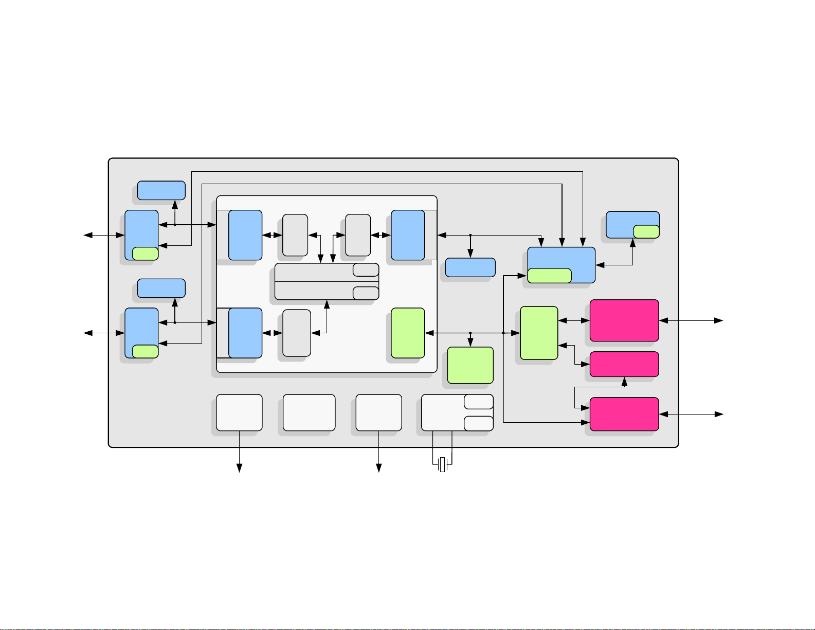
Revision 1.4 (08-19-08) 21 SMSC LAN9311/LAN9311i
2.2 Block Diagram
IEEE 1588
Time Stamp
Datasheet
Two Port 10/100 Managed Ethernet Switch with 16-Bit Non-PCI CPU Interface
DATASHEET
To Ethernet
To Ethernet
10/100
MII
PHY
Registers
MDIO
IEEE 1588
Time Stamp
10/100
MII
PHY
Registers
MDIO
LAN9311/LAN9311i
To optional GPIOs/LEDs
Port 1
10/100
MAC
Port 2
10/100
MAC
GPIO/LED
Controller
4 Queues
Dynamic
QoS
4 Queues
QoS
Dynamic
10/100
Port 0
MAC
Switch Engine
Buffer Manager
4 Queues
Dynamic
QoS
Search
Engine
Frame
Buffers
Switch
IEEE 1588
Time Stamp
Registers
(CSRs)
System
Switch Fabric
IEEE 1588
Time Stamp
Clock/Events
System
Interrupt
Controller
IRQ
Registers
System
Clocks/
Reset/PME
Controller
External
(CSRs)
GP Timer
Free-Run
Clk
25MHz Crystal
Figure 2.1 Internal LAN9311/LAN9311i Block Diagram
MII
Host MAC
TX/RX FIFOs
Register
Access
MUX
MDIO
MDIO
EEPROM Controller
Virtual PHY
Registers
MDIO
Host Bus Interface
EEPROM Loader
I2C (master)
Microwire (master)
To 16-bit
Host Bus
2
I
C/Microwire
To optional
EEPROM
Page 22

Two Port 10/100 Managed Ethernet Switch with 16-Bit Non-PCI CPU Interface
2.2.1 System Clocks/Reset/PME Controller
A clock module contained within the LAN9311/LAN9311i generates all the system clocks required by
the device. This module interfaces directly with the external 25MHz crystal/oscillator to generate the
required clock divisions for each internal module, with the exception of the 1588 clocks, which are
generated in the 1588 Time Stamp Clock/Events module. A 16-bit general pu rpose timer and 32-bit
free-running clock are provided by this module for general purpo se use.
The LAN9311/LAN9311i reset events are categorized as chip-level resets, multi-module resets, and
single-module resets.
A chip-level reset is initiated by assertion of any of the fo llowing input events:
Power-On Reset
nRST Pin Reset
A multi-module reset is initiated by assertion of the fo llowing:
Digital Reset - DIGITAL_RST (bit 0) in the Reset Control Register (RESET_CTL)
- Resets all LAN9311/LAN9311i sub-modules except the Ethernet PHYs (Port 1 PHY, Port 2 PHY,
and Virtual PHY)
Soft Reset - SRST (bit 0) in the Hardware Configuration Register (HW_CFG)
- Resets the HBI, Host MAC, and System CSRs below address 100h
Datasheet
A single-module reset is initiated by assertion of the following:
Port 2 PHY Reset - PHY2_RST (bit 2) in the Reset Control Register (RESET_CTL) or Reset (bit
15) in the Port x PHY Basic Control Register (PHY_BASIC_CONTROL_x)
- Resets the Port 2 PHY
Port 1 PHY Reset - PHY1_RST (bit 1) in the Reset Control Register (RESET_CTL) or Reset (bit
15) in the Port x PHY Basic Control Register (PHY_BASIC_CONTROL_x)
- Resets the Port 1 PHY
Virtual PHY Reset - VPHY_RST (bit 0) in the Reset Control Register (RESET_CTL), (bit 10) in
the Power Manag ement Control Register (PMT_CTRL), or Reset (bit 15) in the Virtual PHY Basic
Control Register (VPHY_BASIC_CTRL)
- Resets the Virtual PHY
The LAN9311/LAN9311i supports numerous power management and wakeup featu res. The Port 1 &
2 PHYs provide general power-down and energy detect power-down modes, which allo w a reduction
in PHY power consumption. The Host MAC provides wake-up frame detection and magic packet
detection modes. The LAN9311/LAN9311i can be programmed to issue an external wake signal (PME)
via several methods, including wake on LAN, wake on link status change (energy detect), and magic
packet wakeup. The PME signal is ideal for triggering system power-up using remote Ethernet wakeup
events.
2.2.2 System Interrupt Controller
The LAN9311/LAN9311i provides a multi-tier programmable interrupt structure which is co ntrolled by
the System Interrupt Controller. At the top level are the Interrupt Status Register (INT_STS) and
Interrupt Enable Register (INT_EN). These registers aggregate and control all interrupts from the
various LAN9311/LAN9311i sub-modules. The LAN9311/LAN9311i is capable of generating interrupt
events from the following:
1588 Time Stamp
Switch Fabric
Ethernet PHYs
GPIOs
Host MAC (FIFOs, power management)
Revision 1.4 (08-19-08) 22 SMSC LAN9311/LAN9311i
DATASHEET
Page 23

Two Port 10/100 Managed Ethernet Switch with 16-Bit Non-PCI CPU Interface
Datasheet
General Purpose Timer
Software (general purpose)
A dedicated programmable IRQ interrupt output pin is provided for external indication of any
LAN9311/LAN9311i interrupts. The IRQ pin is controlled via the Interrupt Configuration Register
(IRQ_CFG), which allows configuration of the IRQ buffer type, polarity, and de-assertion interval.
2.2.3 Switch Fabric
The Switch Fabric consists of the following major function blocks:
10/100 MACs
There is one 10/100 Ethernet MAC per switch fabric port, which provid es basic 10/100 Ethernet
functionality, including transmission deferral, collision back-off/retry, TX/RX FCS
checking/generation, TX/RX pause flow control, and transmit back pressure. The 10/1 00 MACs act
as an interface between the switch engine and the 10/1 00 PHYs (for ports 1 and 2). The port 0
10/100 MAC interfaces the switch engine to the Host MAC. Each 10/100 MAC i ncludes RX and
TX FIFOs and per port statistic counters.
Switch Engine
This block, consisting of a 3 port VLAN layer 2 switching engine, provides the control for all
forwarding/filtering rules and supports untagged, VLAN tagged, and priority tagged frames. The
switch engine provides an extensive feature set which includes spanning tree protocol su pport,
multicast packet filtering and Quality of Service (QoS) packet prioritization by VLAN tag, destination
address, and port default value or DIFFSERV/TOS, allowing for a range of prioritization
implementations. A 1K entry forwarding table provides ample room for MAC address forwarding
tables.
Buffer Manager
This block controls the free buffer space, multi-level transmit queues, transmission scheduling, and
packet dropping of the switch fabric. 32K of buffer RAM allows for the storage of multiple packets
while forwarding operations are completed. Each port is allocated 1a cluster of 4 dynamic QoS
queues which allow each queue size to grow and shrink with tra ffic, effectively utilizing all available
memory. This memory is managed dynamically via the Buffer Manager block.
Switch CSRs
This block contains all switch related control and status registers, and allows all aspects of the
switch fabric to be managed. These registers are indirectly accessibl e via the memory mapped
system control and status registers
2.2.4 Ethernet PHYs
The LAN9311/LAN9311i contains three PHYs: Port 1 PHY, Port 2 PHY and a Virtual PHY. The Port 1
& 2 PHYs are identical in functionality and each connect thei r corresponding Ethernet signal pins to
the switch fabric MAC of their respective port. These PHYs interface with their respective MAC via an
internal MII interface. The Virtual PHY provides the virtual functionality of a PH Y and al lows connecti on
of the Host MAC to port 0 of the switch fabric as if it was connected to a single port PHY. All PHYs
comply with the IEEE 802.3 Physical Layer for Twisted Pair Ethernet and can be configured for full/half
duplex 100 Mbps (100BASE-TX) or 10Mbps (10BASE-T) Ethernet operation. All PHY registers follow
the IEEE 802.3 (clause 22.2.4) specified MII management register se t.
2.2.5 Host Bus Interface (HBI)
The Host Bus Interface (HBI) module provides a high-speed asynchronous SRAM-like slave interface
that facilitates communication between the LAN9311/LAN9311i and a host system. The HBI allows
access to the System CSRs and handles byte swapping based on the dynamic endianess select. The
HBI interfaces to the switch fabric via the Host MAC, which contains the TX/RX Data and Status FIFOs,
Host MAC registers and power management features. The main features of the HBI are:
Asynchronous 16-bit Host Bus Interface
- Host Data Bus Endianess Control
- Direct FIFO Access Modes
SMSC LAN9311/LAN9311i 23 Revision 1.4 (08-19-08)
DATASHEET
Page 24

System CSRs Access
Interrupt Support
2.2.6 Host MAC
The Host MAC incorporates the essential protocol requirements for operating an Ethernet/IEEE 802.3compliant node and provides an interface between the Host Bus Interface (HBI) and the Ethernet PHYs
and Switch Fabric. On the front end, the Host MAC interfaces to the HBI via 2 sets of FIFO’s (TX Data
FIFO, TX Status FIFO, RX Data FIFO, RX Status FIFO). The FIFOs are a conduit between the HBI
and the Host MAC through which all transmitted and received data and status information is passed.
An additional bus is used to access the Host MAC CSR’s via the Host MAC CSR Interface Command
Register (MAC_CSR_CMD) and Host MAC CSR Interface Data Register (MAC_CSR_DATA) system
registers.
On the back end, the Host MAC interfaces with the 10/100 Ethernet PHY’s (Virtual PHY, Port 1 PHY,
Port 2 PHY) via an internal SMI (Serial Management Interface) bus. This allows the Host MAC access
to the PHY’s internal registers via the Host MAC MII Access Register (HMAC_MII_ACC) and Host
MAC MII Data Register (HMAC_MII_DATA). The Host MAC interfaces to the Switch Engine Port 0 via
an internal MII (Media Independent Interface) connection allowing for incoming and outgoi ng Ethernet
packet transfers.
The Host MAC can operate at either 100Mbps or 10Mbps in both half-duplex or full-duplex modes.
When operating in half-duplex mode, the Host MAC complies fully with Section 4 of ISO/IEC 8802-3
(ANSI/IEEE standard) and ANSI/IEEE 802.3 standards. When operating in full-duplex mode, the Host
MAC complies with IEEE 802.3 full-duplex operation standard.
Two Port 10/100 Managed Ethernet Switch with 16-Bit Non-PCI CPU Interface
Datasheet
2.2.7 EEPROM Controller/Loader
The EEPROM Controller is an I2C/Microwire master module which interfaces an optional external
EEPROM with the system register bus and the EEPROM Loader. Multiple types (I2C/Microwire) and
sizes of external EEPROMs are supported. Configuration of the EEPROM type and size are
accomplished via the eeprom_type_strap and eeprom_size_strap[1:0] configuration straps respectively.
Various commands are supported for each EEPROM type, allowing for the storage and retrieval of
static data. The I
The EEPROM Loader module interfaces to the EEPROM Controller, Ethernet PHYs, and the system
CSRs. The EEPROM Loader provides the automatic loading of configuration settings from the
EEPROM into the LAN9311/LAN9311i at reset. The EEPROM Loader runs upon a pin reset (nRST),
power-on reset (POR), digital reset (DIGITAL_RST bit in the Reset Control Register (RESET_CTL)),
or upon the issuance of a RELOAD command via the EEPROM Command Register (E2P_CMD).
2
C interface conforms to the Philips I2C-Bus Specification.
2.2.8 1588 Time Stamp
The IEEE 1588 Time Stamp modules provide hardware support for the IEEE 1588 Precision Time
Protocol (PTP), allowing clock synchronization with remote Ethernet devices, packet time stamping,
and time driven event generation. Time stamping is supported on all ports, with an individual IEEE
1588 Time Stamp module connected to each port via the MII bus. Any port may function as a master
or a slave clock per the IEEE 1588 specification, and the LAN9311/LAN9311i as a whole may function
as a boundary clock.
A 64-bit tunable clock is provided that is used as the time source for all IEEE 1588 time stamp related
functions. The IEEE 1588 Clock/Events block provides IEEE 1588 clock comparison based interrupt
generation and time stamp related GPIO event generation. Two LAN9311/LAN9311i GPIO pins
(GPIO[8:9]) can be used to trigger a time stamp capture when configured as an input, or output a
signal from the GPIO based on an IEEE 1588 clock target compare event when configured as an
output. All features of the IEEE 1588 hardware time stamp unit can be monitored and configured via
their respective IEEE 1588 configuration and status registers (CSRs).
Revision 1.4 (08-19-08) 24 SMSC LAN9311/LAN9311i
DATASHEET
Page 25
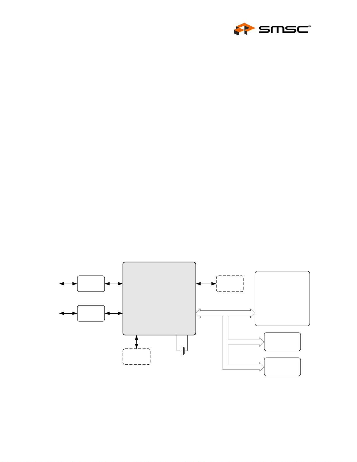
Two Port 10/100 Managed Ethernet Switch with 16-Bit Non-PCI CPU Interface
Datasheet
2.2.9 GPIO/LED Controller
The LAN9311/LAN9311i provides 12 configurable general-purpose input/output pins which are
controlled via this module. These pins can be individually configured via the GPIO/LED CSRs to
function as inputs, push-pull outputs, or open drain outputs and each is capable of interrupt generation
with configurable polarity. Two of the GPIO pins (GPIO[9:8]) can be used for IEEE 1588 timestamp
functions, allowing GPIO driven 1588 time clock capture when configured as an input, or GPIO output
generation based on an IEEE 1588 clock target compare event.
In addition, 8 of the GPIO pins can be alternatively configured as LED outputs. These pins, GPIO[7:0]
(nP1LED[3:0] and nP2LED[3:0]), may be enabled to drive Ethernet status LEDs for external indication
of various attributes of the switch ports.
2.3 System Configuration
In a typical application, the LAN9311/LAN9311i Host Bus Interface (HBI) is connected to the host
microprocessor/microcontroller via the asynchronous 16-bit interface, allowing access to the
LAN9311/LAN9311i system configuration and status registers. The LAN9311/LAN9311i utilizes the
internal Host MAC to provide a network path for the host CPU. The LAN9311/LAN9311i may share the
host bus with additional system memory and/or peripherals. For more information on the HBI, refer to
Chapter 8, "Host Bus Interface (HBI)," on page 99.
The 2 Ethernet ports of the LAN9311/LAN9311i must be connected to Auto-MDIX style magnetics for
proper operation on the Ethernet network. Refer to the SMSC Application Note 8.13 “Suggested
Magnetics” for further details.
To Ethernet
To Ethernet
The LAN9311/LAN9311i also supports optional EEPROM and GPIOs/LEDs. When an EEPROM is
connected, the EEPROM loader can be used to load th e initial device configuration from the external
EEPROM via the I
2
C/Microwire interface.
A system configuration diagram of the LAN9311/LAN9311i in a typical embedded en vironment can be
seen in Figure 2.2.
Magnetics
Magnetics
LAN9311/LAN9311i
GPIOs/LEDs
(optional)
I2C/Microwire
External
25MHz Crystal
EEPROM
(optional)
Microprocessor/
Microcontroller
System
Memory
System
Peripherals
Figure 2.2 System Block Diagram
SMSC LAN9311/LAN9311i 25 Revision 1.4 (08-19-08)
DATASHEET
Page 26
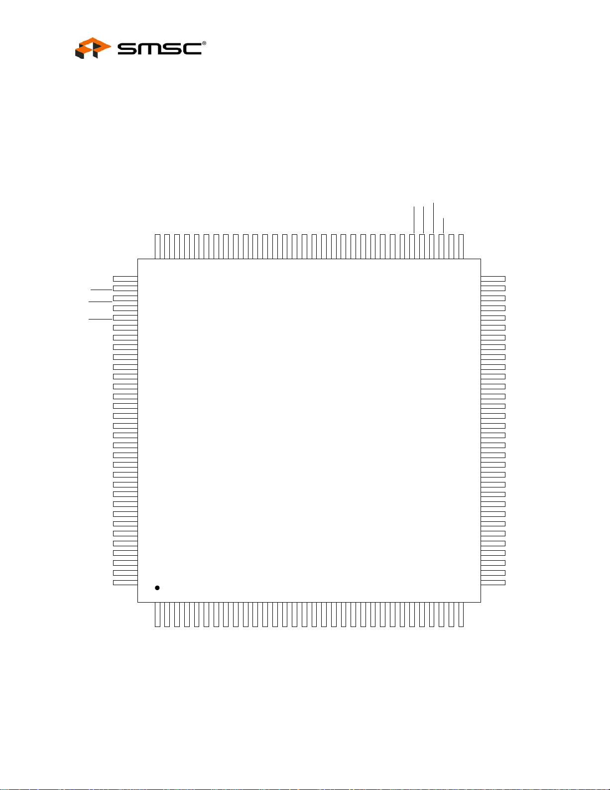
Two Port 10/100 Managed Ethernet Switch with 16-Bit Non-PCI CPU Interface
Chapter 3 Pin Description and Configuration
3.1 Pin Diagrams
3.1.1 128-VTQFP Pin Diagram
Datasheet
EEDO/EEPROM_TYPE
EECLK/EE_SCL/
EEPROM_SIZE_1
VDD33IO
EECS/EEPROM_SIZE_0
VDD18CORE
VDD18PLL
TEST2
TXN1
TXP1
VDD33A1
RXN1
RXP1
VDD33A1
VDD18TX1
EXRES
VDD33BIAS
VDD18TX2
VDD33A2
RXP2
RXN2
VDD33A2
TXP2
TXN2
EEDI/EE_SDANCNC
96959493929190898887868584838281807978777675747372717069686766
97VSS
98
99
100
101
NC
NC
XI
XO
NC
VSS
VSS
VSS
102
103
104
105
106
107
108
109
110
111
112
113
114
115
116
117
118
119
120
121
122
123
124
125
126
127
128
nP1LED0/GPIO0
VDD33IO
nP1LED2/GPIO2
nP1LED1/GPIO1
VDD18CORE
nP1LED3/GPIO3
nP2LED0/GPIO4
VDD33IO
nP2LED2/GPIO6
nP2LED1/GPIO5
GPIO8
nP2LED3/GPIO7
VSS
VDD33IO
GPIO10
GPIO9NCGPIO11
SMSC
LAN9311
128-VTQFP
TOP VIEW
VDD18CORE
TEST1
VDD33IO
VDD33IO
AUTO_MDIX_2
nRST
PHY_ADDR_SEL
AUTO_MDIX_1
VDD33IO
LED_EN
VDD18CORE
65
64
63
62
61
60
59
58
57
56
55
54
53
52
51
50
49
48
47
46
45
44
43
42
41
40
39
38
37
36
35
34
33
VDD33IO
IRQ
PME
END_SEL
FIFO_SEL
nCS
nWR
nRD
A1
A2
VDD33IO
A3
A4
A5
A6
A7
VSS
A8
VDD33IO
A9
D0
D1
D2
D3
VDD18CORE
VDD33IO
D4
D5
D6
D7
D8
VDD33IO
12345678910111213141516171819202122232425262728293031
NC
NCNCNC
VDD18CORE
NCNCNCNCNC
VDD33IO
NC
NC
NCNCNC
VDD33IO
NCNCNC
VSS
VDD18CORE
VDD33IO
NC
D15
D14
D13
VDD33IO
32
D9
D12
D10
D11
Figure 3.1 LAN9311 128-VTQFP Pin Assignments (TOP VIEW)
Revision 1.4 (08-19-08) 26 SMSC LAN9311/LAN9311i
DATASHEET
Page 27
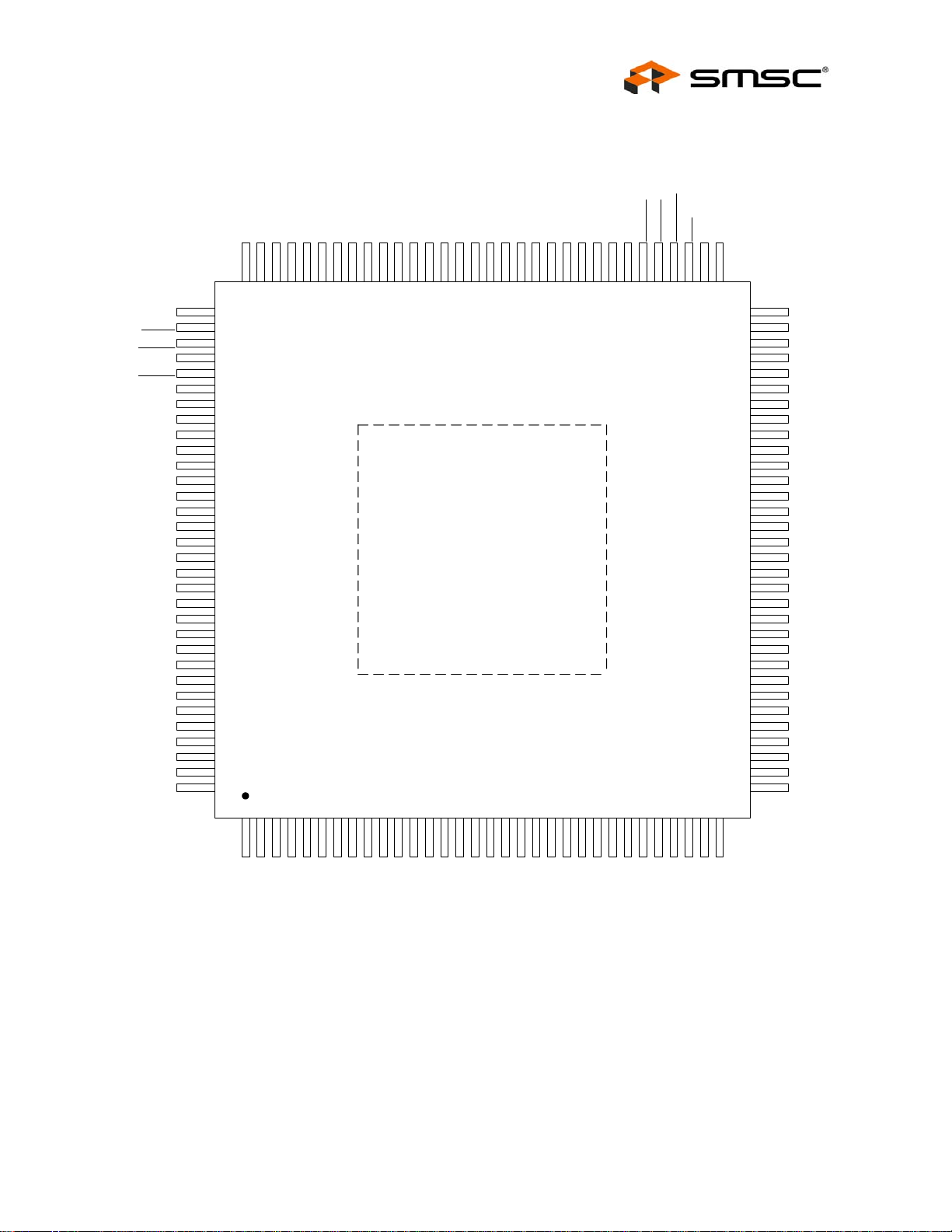
Two Port 10/100 Managed Ethernet Switch with 16-Bit Non-PCI CPU Interface
Datasheet
3.1.2 128-XVTQFP Pin Diagram
EEDO/EEPROM_TYPE
EECLK/EE_SCL/
EEPROM_SIZE_1
VDD33IO
EECS/EEPROM_SIZE_0
VDD18CORE
VDD18PLL
TEST2
TXN1
TXP1
VDD33A1
RXN1
RXP1
VDD33A1
VDD18TX1
EXRES
VDD33BIAS
VDD18TX2
VDD33A2
RXP2
RXN2
VDD33A2
TXP2
TXN2
EEDI/EE_SDANCNC
96959493929190898887868584838281807978777675747372717069686766
97VSS
98
99
100
NC
NC
XI
XO
NC
VSS
VSS
VSS
101
102
103
104
105
106
107
108
109
110
111
112
113
114
115
116
117
118
119
120
121
122
123
124
125
126
127
128
nP1LED0/GPIO0
VDD33IO
nP1LED2/GPIO2
nP1LED1/GPIO1
VDD18CORE
nP1LED3/GPIO3
nP2LED0/GPIO4
VDD33IO
nP2LED2/GPIO6
nP2LED1/GPIO5
GPIO8
nP2LED3/GPIO7
VSS
VDD33IO
GPIO10
GPIO9NCGPIO11
SMSC
LAN9311/LAN9311i
128-XVTQFP
TOP VIEW
VSS
VDD18CORE
TEST1
VDD33IO
VDD33IO
AUTO_MDIX_2
nRST
PHY_ADDR_SEL
AUTO_MDIX_1
VDD33IO
LED_EN
VDD18CORE
65
64
63
62
61
60
59
58
57
56
55
54
53
52
51
50
49
48
47
46
45
44
43
42
41
40
39
38
37
36
35
34
33
VDD33IO
IRQ
PME
END_SEL
FIFO_SEL
nCS
nWR
nRD
A1
A2
VDD33IO
A3
A4
A5
A6
A7
VSS
A8
VDD33IO
A9
D0
D1
D2
D3
VDD18CORE
VDD33IO
D4
D5
D6
D7
D8
VDD33IO
12345678910111213141516171819202122232425262728293031
NC
NCNCNC
VDD18CORE
NCNCNCNCNC
VDD33IO
NOTE: EXPOSED PAD ON BOTTOM OF PACKAGE MUST BE CONNECTED TO GROUND
NC
NC
NCNCNC
VDD33IO
VDD18CORE
VSS
NCNCNC
VDD33IO
NC
D15
D14
D13
VDD33IO
32
D9
D12
D10
D11
Figure 3.2 LAN9311/LAN9311i 128-XVTQFP Pin Assignments (TOP VIEW)
SMSC LAN9311/LAN9311i 27 Revision 1.4 (08-19-08)
DATASHEET
Page 28

3.2 Pin Descriptions
This section contains the descriptions of the LAN9311/LAN9311i pins. The pin descriptions have been
broken into functional groups as follows:
LAN Port 1 Pins
LAN Port 2 Pins
LAN Port 1 & 2 Power and Common Pins
Host Bus Interface Pins
EEPROM Pins
Dedicated Configuration Strap Pins
Miscellaneous Pins
PLL Pins
Core and I/O Power and Ground Pins
No-Connect Pins
Note: A list of b uffer type definitions is provided in Section 1.2, "Buffer Types," on page 18.
Two Port 10/100 Managed Ethernet Switch with 16-Bit Non-PCI CPU Interface
Datasheet
Table 3.1 LAN Port 1 Pins
PIN NAME SYMBOL
Port 1 LED
nP1LED[3:0] OD12 LED Indicators: When configured as LED outputs
Indicators
General
GPIO[3:0] IS/O12/
Purpose I/O
89-92
110
Data
Port 1
Ethernet TX
TXN1 AIO Ethernet TX Negative: Negative output of Port 1
Negative
111
Port 1
Ethernet TX
TXP1 AIO Ethernet TX Positive: Positive output of Port 1
Positive
BUFFER
TYPE DESCRIPTION
via the LED Configuration Register (LED_CFG),
these pins are open-drain, active low outputs and
the pull-ups and input buffers are disabled. The
functionality of each pin is determined via the
LED_CFG[9:8] bits.
General Purpose I/O Data: When configured as
OD12
(PU)
GPIO via the LED Configuration Register
(LED_CFG), these general purpose signals are
fully programmable as either push-pull outputs,
open-drain outputs or Schmitt-triggered inputs by
writing the General Purpose I/O Configuration
Register (GPIO_CFG) and General Purpose I/O
Data & Direction Register (GPIO_DATA_DIR). The
pull-ups are enabled in GPIO mode. The input
buffers are disabled when set as an output.
Note: See Chapter 13, "GPIO/LED Controller,"
on page 163 for additional details.
Ethernet transmitter. See Note 3.1 for additiona l
information.
Ethernet transmitter. See Note 3.1 for additional
information.
Port 1
115
Ethernet RX
Negative
Port 1
116
Ethernet RX
Positive
Revision 1.4 (08-19-08) 28 SMSC LAN9311/LAN9311i
RXN1 AIO Ethernet RX Negative: Negative input of Port 1
Ethernet receiver. See Note 3.1 for additiona l
information.
RXP1 AIO Ethernet RX Positive: Positive input of Port 1
Ethernet receiver. See Note 3.1 for additiona l
information.
DATASHEET
Page 29

Two Port 10/100 Managed Ethernet Switch with 16-Bit Non-PCI CPU Interface
Datasheet
Note 3.1 The pin names for the twisted pair pins apply to a normal connection. If HP Auto-MDIX is
enabled and a reverse connection is detected or manually se lected, the RX and TX pins
will be swapped internally.
Table 3.2 LAN Port 2 Pins
BUFFER
PIN NAME SYMBOL
TYPE DESCRIPTION
83-86
127
126
124
Port 2 LED
Indicators
General
Purpose I/O
Data
Port 2
Ethernet TX
Negative
Port 2
Ethernet TX
Positive
Port 2
Ethernet RX
Negative
nP2LED[3:0] OD12 LED indicators: When configured as LED outputs
GPIO[7:4] IS/O12/
OD12
(PU)
TXN2 AIO Ethernet TX Negative: Negative output of Port 2
TXP2 AIO Ethernet TX Positive: Positive output of Port 2
RXN2 AIO Ethernet RX Negative: Negative input of Port 2
via the LED Configuration Register (LED_CFG),
these pins are open-drain, active low outputs and
the pull-ups and input buffers are disabled. The
functionality of each pin is determined via the
LED_CFG[9:8] bits.
General Purpose I/O Data: When configured as
GPIO via the LED Configuration Register
(LED_CFG), these general purpose signals are
fully programmable as either push-pull outputs,
open-drain outputs or Schmitt-triggered inputs by
writing the General Purpose I/O Configuration
Register (GPIO_CFG) and General Purpose I/O
Data & Direction Register (GPIO_DATA_DIR). The
pull-ups are enabled in GPIO mode. The input
buffers are disabled when set as an output.
Note: See Chapter 13, "GPIO/LED Controller,"
on page 163 for additional details.
Ethernet transmitter. See Note 3.2 for additiona l
information.
Ethernet transmitter. See Note 3.2 for additional
information.
Ethernet receiver. See Note 3.2 for additiona l
information.
Port 2
123
PIN NAME SYMBOL
119
114,117
SMSC LAN9311/LAN9311i 29 Revision 1.4 (08-19-08)
Ethernet RX
Positive
Note 3.2 The pin names for the twisted pair pins apply to a normal connection. If HP Auto-MDIX is
enabled and a reverse connection is detected or manually se lected, the RX and TX pins
will be swapped internally.
Bias
Reference
+3.3V Port 1
Analog Power
Supply
RXP2 AIO Ethernet RX Positive: Positive input of Port 2
Ethernet receiver. See Note 3.2 for additiona l
information.
T a ble 3.3 LAN Port 1 & 2 Power and Common Pins
BUFFER
TYPE DESCRIPTION
EXRES AI Bias Reference: Used for internal bias circuits.
Connect to an external 12.4K ohm, 1% resistor to
ground.
VDD33A1 P +3.3V Port 1 Analog Power Supply
Refer to the LAN9311/LAN9311i application note
for additional connection information.
DATASHEET
Page 30

Table 3.3 LAN Port 1 & 2 Power and Common Pins (continued)
PIN NAME SYMBOL
Two Port 10/100 Managed Ethernet Switch with 16-Bit Non-PCI CPU Interface
Datasheet
BUFFER
TYPE DESCRIPTION
122,125
120
121
118
+3.3V Port 2
Analog Power
Supply
+3.3V Master
Bias Power
Supply
Port 2
Transmitter
+1.8V Power
Supply
Port 1
Transmitter
+1.8V Power
Supply
VDD33A2 P +3.3V Port 2 Analog Power Supply
Refer to the LAN9311/LAN9311i application note
for additional connection information.
VDD33BIAS P +3.3V Master Bias Power Supply
Refer to the LAN9311/LAN9311i application note
for additional connection information.
VDD18TX2 P Port 2 Transmitter +1.8V Power Supply: This pin
is supplied from the internal PHY voltage regulator.
This pin must be tied to the VDD18TX1 pin for
proper operation.
Refer to the LAN9311/LAN9311i application note
for additional connection information.
VDD18TX1 P +1.8V Port 1 Transmitter Power Supply: This pin
must be connected directly to the VDD18TX2 pin
for proper operation.
Refer to the LAN9311/LAN9311i application note
for additional connection information.
Table 3.4 Host Bus Interface Pins
PIN NAME SYMBOL
25,26,
28-32,
34-38,
41-44
45,47,
49-53,
55,56
57
58
59
Host Bus
Data
Host Bus
Address
Read Strobe nRD IS Read Strobe: Active low strobe to indicate a read
Write Strobe nWR IS Write Stro be: Active low strobe to indicate a write
Chip Select nCS IS Chip Select: Active low signal used to qualify read
D[15:0] IS/O8 Host Bus Data: Bits 15-0 of the Host Bus data
A[9:1] IS Host Bus Address: 9-bit Host Bu s Address Port
BUFFER
TYPE DESCRIPTION
port.
Note: Big and little endianess is supported.
used to select Internal CSR’s and TX and RX
FIFO’s.
Note: The A0 bit is not used because the
LAN9311/LAN9311i must be accessed on
WORD boundaries.
cycle. This signal is qualified by the nCS chip
select.
cycle. This signal is qualified by the nCS chip
select.
and write operations.
Revision 1.4 (08-19-08) 30 SMSC LAN9311/LAN9311i
DATASHEET
Page 31

Two Port 10/100 Managed Ethernet Switch with 16-Bit Non-PCI CPU Interface
Datasheet
Table 3.4 Host Bus Interface Pins (continued)
BUFFER
PIN NAME SYMBOL
TYPE DESCRIPTION
Data FIFO
FIFO_SEL IS Data FIFO Direct Access Select: When driven
Direct Access
Select
60
Endianess
END_SEL IS Endianess Select: When this signal is set high,
Select
61
Note: Refer to Chap ter 8, "Host Bus Interface (HBI)," on page 99 for additional informati on regarding
the use of these signals.
PIN NAME SYMBOL
EEPROM
EEDI IS
Microwire
Data Input
96
EEPROM I
2
C
EE_SDA IS/OD8 EEPROM I2C Serial Data Input/Output
Serial Data
Input/Output
high, all accesses to the LAN9311/LAN9311i are
directed to the RX and TX Data FIFO’s. All reads
are from the RX Data FIFO, and all writes are to
the TX Data FIFO. In this mode, the address input
is ignored. Refer to Section 14.1.3, "Direct FIFO
Access Mode," on page 168 for additional
information.
big endian mode is selected. When low, little
endian mode is selected. This signal may be
dynamically changed or held static. Refer to
Chapter 8, "Host Bus Interface (HBI)," on page 99
for additional information.
Table 3.5 EEPROM Pins
BUFFER
TYPE DESCRIPTION
EEPROM Microwire Data Input (EEDI): In
(PD)
Microwire EEPROM mode (EEPROM_TYPE = 0),
this pin is the Microwire EEPROM serial data input.
(EE_SDA): In I2C EEPROM mode
(EEPROM_TYPE = 1), this pin is the I2C EEPROM
serial data input/output.
98
99
EEPROM
Microwire
Data Output
EEPROM
Type Strap
EEPROM
Microwire
Serial Clock
EEPROM I
Serial Clock
EEPROM
Size Strap 1
2
C
EEDO O8 EEPROM Microwire Data Output: In Microwire
EEPROM mode (EEPROM_TYPE
= 0), this pin is
the Microwire EEPROM serial data output.
Note: In I
2
C mode (EEPROM_TYPE=1), this pin
is not used and is driven low.
EEPROM_TYPE
IS
Note 3.3
EEPROM Type Strap: Configures the EEPROM
type. See Note 3.4
0 = Microwire Mode
2
1 = I
C Mode
EECLK O8 EEPROM Microwire Serial Clock (EECLK): In
Microwire EEPROM mode (EEPROM_TYPE
this pin is the Microwire EEPROM clock output.
EE_SCL IS/OD8 EEPROM I2C Serial Clock (EE_SCL): In I2C
EEPROM mode (EEPROM_TYPE=1), this pin is
the I2C EEPROM clock input/open-drain output.
EEPROM_SIZE_1
IS
Note 3.5
EEPROM Size Strap 1: Configures the high bit of
the EEPROM size range as specified in Section
= 0),
10.2, "I2C/Microwire Master EEPROM Controller,"
on page 138. This bit is not used for I2C
EEPROMs. See Note 3.4.
SMSC LAN9311/LAN9311i 31 Revision 1.4 (08-19-08)
DATASHEET
Page 32

PIN NAME SYMBOL
Two Port 10/100 Managed Ethernet Switch with 16-Bit Non-PCI CPU Interface
Datasheet
Table 3.5 EEPROM Pins (continued)
BUFFER
TYPE DESCRIPTION
EEPROM
EECS O8 EEPROM Microwire Chip Select: In Microwire
Microwire
Chip Select
101
EEPROM
EEPROM_SIZE_0
Size Strap 0
Note 3.3 The IS buffer type is valid only during the time specified in Section 15.5.2, "Reset and
Configuration Strap Timing," on page 446.
Note 3.4 Configuration strap values are latched on power-on reset or nRST de-assertion.
Configuration strap pins are identified by an underlined symbol name. Refer to Section
4.2.4, "Configuration Straps," on page 40 for more information.
Note 3.5 The IS buffer type is valid only during the time specified in Section 15.5.2, "Reset and
Configuration Strap Timing," on page 446 and when in I
Table 3.6 Dedicated Configuration Strap Pins
PIN NAME SYMBOL
LED Enable
LED_EN
Strap
67
EEPROM mode (EEPROM_TYPE
the Microwire EEPROM chip select output.
Note: In I2C mode (EEPROM_TYPE=1), this pin
is not used and is driven low.
IS
Note 3.3
EEPROM Size Strap 0: Configures the low bit of
the EEPROM size range as specified in Section
10.2, "I2C/Microwire Master EEPROM Controller,"
on page 138. See Note 3.4.
2
C mode.
BUFFER
TYPE DESCRIPTION
IS
(PU)
LED Enable Strap: Configures the default value
for the LED_EN bits in the LED Configuration
Register (LED_CFG). When latched low, all 8
LED/GPIO pins are configured as GPIOs. When
latched high, all 8 LED/GPIO pins are configured
as LEDs. See Note 3.6.
= 0), this pin is
PHY Address
Strap
PHY_ADDR_SEL
IS
(PU)
PHY Address Select Strap: Configures the default
MII management address values for the PHYs
(Virtual, Port 1, and Port 2) as detailed in Section
7.1.1, "PHY Addressing," on page 82 .
68
VALUE
PHY_ADDR_SEL
ADDRESS
VIRTUAL PHY
ADDRESS
PORT 1 PHY
ADDRESS
PORT 2 PHY
0 012
1 123
See Note 3.6.
Revision 1.4 (08-19-08) 32 SMSC LAN9311/LAN9311i
DATASHEET
Page 33

Two Port 10/100 Managed Ethernet Switch with 16-Bit Non-PCI CPU Interface
Datasheet
Table 3.6 Dedicated Configuration Strap Pins (continued)
BUFFER
PIN NAME SYMBOL
TYPE DESCRIPTION
Port 1 Auto-
AUTO_MDIX_1
MDIX Enable
69
Strap
Port 2 Auto-
AUTO_MDIX_2
MDIX Enable
70
Strap
Note: For more information on configuration straps, refer to Section 4.2.4, "Configuration Straps," on
page 40. Additional strap pins, which share functionality wi th the EEPROM pins, are described
in Table 3.5.
Note 3.6 Configuration strap values are latched on power-on reset or nRST de-assertion.
Configuration strap pins are identified by an underlined symbol name. Some configuration
straps can be overridden by values from the EEPROM Loader. Refer to Section 4.2.4,
"Configuration Straps," on page 40 for more information.
Table 3.7 Miscellaneous Pins
PIN NAME SYMBOL
IS
(PU)
Port 1 Auto-MDIX Enable Strap: Configures the
Auto-MDIX functionality on Port 1. When latched
low, Auto-MDIX is disabled. When latched high,
Auto-MDIX is enabled.
See Note 3.6.
IS
(PU)
Port 2 Auto-MDIX Enable Strap: Configures the
Auto-MDIX functionality on Port 2. When latched
low, Auto-MDIX is disabled. When latched high,
Auto-MDIX is enabled.
See Note 3.6.
BUFFER
TYPE DESCRIPTION
77-79,
82
63
71
General
Purpose I/O
Data
Interrupt
Output
System Reset
Input
GPIO[11:8] IS/OD12/
O12
(PU)
Note 3.7
General Purpose I/O Data: These general
purpose signals are fully programmable as either
push-pull outputs, open-drain outputs, or Schmitttriggered inputs by writing the General Purpose I/O
Configuration Register (GPIO_CFG) and General
Purpose I/O Data & Direction Register
(GPIO_DATA_DIR). For more information, refer to
Chapter 13, "GPIO/LED Controller," on page 163.
Note: The remaining GPIO[7:0] pins share
functionality with the LED output pins, as
described in Table 3.1 a nd Table 3.2.
IRQ O8/OD8 Interrupt Output: Interrupt request output. The
polarity, source and buffer type of this signal is
programmable via the Interrupt Configuration
Register (IRQ_CFG). For more information, refer to
Chapter 5, "System Interrupts," on page 49.
nRST IS
(PU)
System Reset Input: This active low signal allows
external hardware to reset the LAN9311/LAN9311i.
The LAN9311/LAN9311i also contains an internal
power-on reset circuit. Thus, this signal may be left
unconnected if an external hardware reset is not
needed. When used, this signal must adhere to the
reset timing requirements as detailed in Section
15.5.2, "Reset and Configuration Strap Timing," on
page 446.
Note: The LAN9311/LAN9311i must always be
read at least once after power-up or reset
to ensure that write operations function
properly.
SMSC LAN9311/LAN9311i 33 Revision 1.4 (08-19-08)
DATASHEET
Page 34

PIN NAME SYMBOL
Two Port 10/100 Managed Ethernet Switch with 16-Bit Non-PCI CPU Interface
Datasheet
Table 3.7 Miscellaneous Pins (continued)
BUFFER
TYPE DESCRIPTION
75
108
62
PIN NAME SYMBOL
107
Test 1 TEST1 AI Test 1: This pin must be tied to VDD33IO for
Test 2 TEST2 AI Test 2: This pin must be tied to VDD33IO for
Power
Management
Event
Note 3.7 The input buffers are enabled when configured as GPIO inputs only.
PLL +1.8V
Power Supply
PME O8/OD8 Power Management Event: When programmed
VDD18PLL P PLL +1.8V Power Supply: This pin must be
proper operation.
proper operation.
accordingly, this signal is asserted upon detection
of a wakeup event. The polarity and buffer type of
this signal is programmable via the PME_EN bit of
the Power Management Control Register
(PMT_CTRL).
Refer to Chapter 4, "Clocking, Resets, and Power
Management," on page 36 for additi onal
information on the LAN9311/LAN9311i power
management features.
Table 3.8 PLL Pins
BUFFER
TYPE DESCRIPTION
connected to VDD18CORE for proper operation.
Refer to the LAN9311/LAN9311i application note
for additional connection information.
Crystal Input XI ICLK Crystal Input: External 25MHz crystal input. This
105
106
PIN NAME SYMBOL
7,13,21,27,
33,39,46,
54,64,66,
72,73,81,
87,93,100
3,14,40,65,
74,88,104
Crystal
Output
+3.3V I/O
Power
Digital Core
+1.8V Power
Supply
Output
Table 3.9 Core and I/O Power and Ground Pins
VDD33IO P +3.3V Power Supply for I/O Pins and Internal
VDD18CORE P Digital Core +1.8V Power Supply Output: +1.8V
signal can also be driven by a single-ended clock
oscillator. When this method is used, XO should be
left unconnected.
XO OCLK Crystal Output: External 25MHz crystal output.
BUFFER
TYPE DESCRIPTION
Regulator
Refer to the LAN9311/LAN9311i application note
for additional connection information.
power from the internal core voltage regulator. All
VDD18CORE pins must be tied together for proper
operation.
Refer to the LAN9311/LAN9311i application note
for additional connection information.
Revision 1.4 (08-19-08) 34 SMSC LAN9311/LAN9311i
DATASHEET
Page 35

Two Port 10/100 Managed Ethernet Switch with 16-Bit Non-PCI CPU Interface
Datasheet
Table 3.9 Core and I/O Power and Ground Pins (continued)
BUFFER
PIN NAME SYMBOL
TYPE DESCRIPTION
18,48,80,
97,112,113,
128
Note 3.8
PIN NAME SYMBOL
1,2, 4-6,
8-12,
15-17,19,
20,22-24,
76,94,95,
102,103,
109
Common
Ground
Note 3.8 Plus external pad for 128-XVTQFP package only
No Connect NC - No Connect: These pins must be left floating for
VSS P Common Ground
Table 3.10 No-Connect Pins
BUFFER
TYPE DESCRIPTION
normal device operation.
SMSC LAN9311/LAN9311i 35 Revision 1.4 (08-19-08)
DATASHEET
Page 36

Two Port 10/100 Managed Ethernet Switch with 16-Bit Non-PCI CPU Interface
Datasheet
Chapter 4 Clocking, Resets, and Power Management
4.1 Clocks
The LAN9311/LAN9311i includes a clock module which provides generation of all syste m clocks as
required by the various sub-modules of the device. The LAN9311/LAN9311i requires a fixed-frequency
25MHz clock source for use by the internal clock oscillator and PLL. This is typically provided by
attaching a 25MHz crystal to the XI and XO pins as specified in Section 15.6, "Clock Circuit," on
page 455. Optionally, this clock can be provided by driving the XI input pin with a single-ended 25MHz
clock source. If a single-ended source is selected, the clock input must run continuously for normal
device operation. The internal PLL generates a fixed 200MHz base clock which is used to derive all
LAN9311/LAN9311i sub-system clocks.
In addition to the sub-system clocks, the clock module is also responsible for generating the clocks
used for the general purpose timer and free-running clock. Refer to Chapter 12, "General Purpose
Timer & Free-Running Clock," on page 162 for additional details.
Note: Crystal specifications are provided in Table 15.15, “LAN9311/LAN9311iCrystal Specifications,”
on page 455.
4.2 Resets
The LAN9311/LAN9311i provides multiple hardware and software reset sources, which allow varying
levels of the LAN9311/LAN9311i to be reset. All resets can be categorized into three reset types as
described in the following sections:
Chip-Level Resets
—Power-On Reset (POR)
—nRST Pin Reset
Multi-Module Resets
—Digital Reset (DIGITAL_RST)
—Soft Reset (SRST)
Single-Module Resets
—Port 2 PHY Reset
—Port 1 PHY Reset
—Virtual PHY Reset
The LAN9311/LAN9311i supports the use of configuration straps to allow automatic custom
configurations of various LAN9311/LAN9311i parameters. These configuration strap values are set
upon de-assertion of all chip-level resets and can be used to easily set the de fault parameters of the
chip at power-on or pin (nRST) reset. Refer to Section 4.2.4, "Configuration Straps," on page 40 for
detailed information on the usage of these straps.
Note: The LAN9 311/LAN9311i EEPROM Loader is run upon a power-on reset, nRST pin reset, and
digital reset. Refer to Section 10.2.4, "EEPROM Loader," on page 150 for additional
information.
Table 4.1 summarize s the effect of the various reset sources on the LAN9311/LAN9311i. Refer to the
following sections for detailed information on each of these reset types.
Revision 1.4 (08-19-08) 36 SMSC LAN9311/LAN9311i
DATASHEET
Page 37

Two Port 10/100 Managed Ethernet Switch with 16-Bit Non-PCI CPU Interface
Datasheet
T able 4.1 Reset Sources and Affected LAN9311/LAN9311i Circuitry
RESET SOURCE
SYSTEM
CLOCKS/RESET/PME
SYS INTERRUPTS
POR XXXXXXXXXX X
nRST Pin XXXXXXXXXX X
Digital Reset XXX XXXXX X
Soft Reset XX
Port 2 PHY X
Port 1 PHY X
Virtu al PHY X
Note 4.1 In the case of a soft reset, the EEPROM Loader is run, but loads only the MAC address
into the Host MAC. No other values are loaded by the EEPROM Loader in this case .
4.2.1 Chip-Level Resets
A chip-level reset event activates all internal resets, effectively resetting the entire LAN9311/LAN9311i.
Configuration straps are latched, and the EEPROM Loader is run as a result of chip-level resets. A
chip-level reset is initiated by assertion of any of the fo llowing input events:
Power-On Reset (POR)
nRST Pin Reset
SWITCH FABRIC
ETHERNET PHYS
HBI
HOST MAC
EEPROM
CONTROLLER
1588 TIME STAMP
GPIO/LED
CONTROLLER
CONFIG. STRAPS
LATCHED
EEPROM LOADER
Note 4.1
RUN
Chip-level reset completion/configuration can be determined by polling the READY bi t of the Hardware
Configuration Register (HW_CFG) or Power Management Control Register (PMT_CTRL) until it is set.
When set, the READY bit indicates that the reset has completed and the device is ready to be
accessed.
With the exception of the Hardware Configuration Register (HW_CFG), Power Management Control
Register (PMT_CTRL), Byte Order Test Register (BYTE_TEST), and Reset Control Register
(RESET_CTL), read access to any internal resources is forbidden while the READY bit is cleared.
Writes to any address are invalid until the READY bit is set.
Note: The LAN9 311/LAN9311i must be read at least once after any chip-level reset to ensure that
write operations function properly.
4.2.1.1 Power-On Reset (POR)
A power-on reset occurs whenever power is initially applied to the LAN9311/LAN9311i, or if the power
is removed and reapplied to the LAN9311/LAN9311i. This event resets all circuitry within the device.
Configuration straps are latched, and the EEPROM Loader is run as a result of this reset.
SMSC LAN9311/LAN9311i 37 Revision 1.4 (08-19-08)
DATASHEET
Page 38

A POR reset typically takes approximately 23mS, plus additional time (91uS for I2C, 28uS for
Microwire) per byte of data loaded from the EEPROM via the EEPROM Loader. A full EEPROM load
(64KB for I
2
C, 2KB for Microwire) will complete in approximately 6.0 seconds for I2C EEPROM, and
80mS for Microwire EEPROM.
4.2.1.2 nRST Pin Reset
Driving the nRST input pin low initiates a chip-level reset. This event resets all circuitry within the
device. Use of this reset input is optional, but when used, it must be driven for the period of time
specified in Section 15.5.2, "Reset and Configuration Strap Timing," on page 446. Configuration straps
are latched, and the EEPROM Loader is run as a result of this reset.
A nRST pin reset typically takes approximately 760uS, plus additional time (91uS for I
Microwire) per byte of data loaded from the EEPROM via the EEPROM Loader. A full EEPROM load
(64KB for I
58mS for Microwire EEPROM.
Note: Th e nRST pin is pulled-high internally. If unused, this signal can be left unconnected. Do not
Please refer to Section Table 3.7, "Miscellaneous Pi ns," on page 33 for a descri ption of the nRST pin.
2
C, 2KB for Microwire) will complete in approximately 6.0 seconds for I2C EEPROM, and
rely on internal pull-up resistors to drive signals external to the device.
4.2.2 Multi-Module Resets
Two Port 10/100 Managed Ethernet Switch with 16-Bit Non-PCI CPU Interface
Datasheet
2
C, 28uS for
Multi-module resets activate multiple internal resets, but do not reset the entire chip. Configuration
straps are not latched upon multi-module resets. A multi-module reset is initiated by assertion of the
following:
Digital Reset (DIGITAL_RST)
Soft Reset (SRST)
Chip-level reset completion/configuration can be determined by polling the READY bi t of the Hardware
Configuration Register (HW_CFG) or Power Management Control Register (PMT_CTRL) until it is set.
When set, the READY bit indicates that the reset has completed and the device is ready to be
accessed.
With the exception of the Hardware Configuration Register (HW_CFG), Power Management Control
Register (PMT_CTRL), Byte Order Test Register (BYTE_TEST), and Reset Control Register
(RESET_CTL), read access to any internal resources is forbidden while the READY bit is cleared.
Writes to any address are invalid until the READY bit is set.
Note: The di gital reset and soft reset do not reset register bits designated as NASR.
Note: The L AN9311/LAN9311i must be read at least once after a multi-module reset to ensure that
write operations function properly.
4.2.2.1 Digital Reset (DIGITAL_RST)
A digital reset is performed by setting the DIGITAL_RST bit of the Reset Control Register
(RESET_CTL). A digital reset will reset all LAN9311/LAN9311i sub-modules except the Ethernet PHYs
(Port 1 PHY, Port 2 PHY, and Virtual PHY). The EEPROM Loader will automatically run following this
reset. Configuration straps are not latched as a result of a digital reset.
A digital reset typically takes approximately 760uS, plus additional time (91uS for I2C, 28uS for
Microwire) per byte of data loaded from the EEPROM via the EEPROM Loader. A full EEPROM load
(64KB for I2C, 2KB for Microwire) will complete in approximately 6.0 seconds for I2C EEPROM, and
58mS for Microwire EEPROM.
Revision 1.4 (08-19-08) 38 SMSC LAN9311/LAN9311i
DATASHEET
Page 39

Two Port 10/100 Managed Ethernet Switch with 16-Bit Non-PCI CPU Interface
Datasheet
4.2.2.2 Soft Reset (SRST)
A soft reset is performed by setting the SRST bit of the Hardware Configuration Register (HW_CFG).
A soft reset will reset the HBI, Host MAC, and System CSRs below address 100h. The soft reset also
clears any TX or RX errors in the Host MAC transmitter and receiver (TXE/RXE). This reset does not
latch the configuration straps. On soft reset, the EEPROM Loader is run, but loads only the MAC
address into the Host MAC. No other values are loaded by the EEPROM Loader in this case.
A soft reset typically takes 590uS, plus an additional time (550uS for I2C, 170uS for Microwire) when
data is loaded from the EEPROM via the EEPROM Loader.
4.2.3 Single-Module Resets
A single-module reset will reset only the specified module. Single-module resets do not latch the
configuration straps or initiate the EEPROM Loader. A single-module reset is initiated by assertion of
the following:
Port 2 PHY Reset
Port 1 PHY Reset
Virtual PHY Reset
4.2.3.1 Port 2 PHY Reset
A Port 2 PHY reset is performed by setting the PHY2_RST bit of the Reset Control Register
(RESET_CTL) or the Reset bit in the Port x PHY Basic Control Register (PHY_BASIC_CONTROL_x).
Upon completion of the Port 2 PHY reset, the PHY2_RST and Reset bits are automatically cleared.
No other modules of the LAN9311/LAN9311i are affected by this reset.
In addition to the methods above, the Port 2 PHY is automatically reset after returning from a PHY
power-down mode. This reset differs in that the PHY power-down mode reset does not reload or reset
any of the PHY registers. Refer to Section 7.2.9, "PHY Power-Down Modes," on page 94 for additional
information.
Port 2 PHY reset completion can be determined by polling the PHY2_RST bit in the Reset Control
Register (RESET_CTL) or the Reset bit in the Port x PHY Basic Control Register
(PHY_BASIC_CONTROL_x) until it clears. Under normal conditions, the PHY2_RST an d Reset bit will
clear approximately 110uS after the Port 2 PHY reset occurrence.
Note: When usin g the Reset bit to reset the Port 2 PHY, register bits designated as NASR are not
reset.
Refer to Section 7.2.10, "PHY Resets," on page 95 for additional information on Port 2 PHY resets.
4.2.3.2 Port 1 PHY Reset
A Port 1 PHY reset is performed by setting the PHY1_RST bit of the Reset Control Register
(RESET_CTL) or the Reset bit in the Port x PHY Basic Control Register (PHY_BASIC_CONTROL_x).
Upon completion of the Port 1 PHY reset, the PHY1_RST and Reset bits are automatically cleared.
No other modules of the LAN9311/LAN9311i are affected by this reset.
In addition to the methods above, the Port 1 PHY is automatically reset after returning from a PHY
power-down mode. This reset differs in that the PHY power-down mode reset does not reload or reset
any of the PHY registers. Refer to Section 7.2.9, "PHY Power-Down Modes," on page 94 for additional
information.
Port 1 PHY reset completion can be determined by polling the PHY1_RST bit in the Reset Control
Register (RESET_CTL) or the Reset bit in the Port x PHY Basic Control Register
(PHY_BASIC_CONTROL_x) until it clears. Under normal conditions, the PHY1_RST an d Reset bit will
clear approximately 110uS after the Port 1 PHY reset occurrence.
SMSC LAN9311/LAN9311i 39 Revision 1.4 (08-19-08)
DATASHEET
Page 40

Note: When usin g the Reset bit to reset the Port 1 PHY, register bits designated as NASR are not
reset.
Refer to Section 7.2.10, "PHY Resets," on page 95 for additional information on Port 1 PHY resets.
4.2.3.3 Virtual PHY Reset
A Virtual PHY reset is performed by setting the VPHY_RST bit of the Reset Control Register
(RESET_CTL), VPHY_RST bit in the Power Management Control Register (PMT_CTRL), or Reset in
the Virtual PHY Basic Control Register (VPHY_BASIC_CTRL). No other modules of the
LAN9311/LAN9311i are affected by this reset.
Virtual PHY reset completion can be determined by polling the VPHY_RST bit in the Reset Control
Register (RESET_CTL), the VPHY_RST bit in the Power Management Control Register (PMT_CTRL) ,
or the Reset bit in the Virtual PHY Basic Control Register (VPHY_BASIC_CTRL) until it clears. Under
normal conditions, the VPHY_RST and Reset bit will clear approximately 1uS after the Virtual PHY
reset occurrence.
Refer to Section 7.3.2, "Virtual PHY Resets," on page 98 for additional information on Virtual PHY
resets.
4.2.4 Configuration Straps
Configuration straps allow various features of the LAN9311/LAN9311i to be automatically configured
to user defined values. Configuration straps can be organized into two main catego ries: hard-straps
and soft-straps. Both hard-straps and soft-straps are latched upon Power-On Reset (POR) or pin reset
(nRST). The primary difference between these strap types is that soft-strap default values can be
overridden by the EEPROM Loader, while hard-straps cannot.
Two Port 10/100 Managed Ethernet Switch with 16-Bit Non-PCI CPU Interface
Datasheet
Configuration straps which have a corresponding external pin include internal resistors in order to
prevent the signal from floating when unconnected. If a particular configuration strap is connected to
a load, an external pull-up or pull-down resistor should be used to augment the internal resistor to
ensure that it reaches the required voltage level prior to latching. The internal resistor can also be
overridden by the addition of an external resistor.
Note: The system designer must guarantee that configuration strap pins meet the timing
requirements specified in Section 15.5.2, "Reset and Configuration Strap Timing," on page 446.
If configuration strap pins are not at the correct voltage level prior to being latched, the
LAN9311/LAN9311i may capture incorrect strap values.
4.2.4.1 Soft-Straps
Soft-strap values are latched on the release of POR or nRST and are overridden b y values from the
EEPROM Loader (when an EEPROM is present). These straps are used as direct configuration values
or as defaults for CPU registers. Some, but not all, soft-straps have an associated pin. Those that do
not have an associated pin, have a tie off default value. All soft-strap values can be overridden by the
EEPROM Loader. Table 4.2 provides a list of all soft-straps and their associated pin or default value.
Straps which have an associated pin are also fully defined in Chapter 3, "Pin Description and
Configuration," on page 26. Refer to Section 10.2.4, "EEPROM Loader," on page 150 for information
on the operation of the EEPROM Loader and the loading of strap va lues.
Upon setting the DIGITAL_RST bit in the Reset Control Register (RESET_CTL) or upon issuing a
RELOAD command via the EEPROM Command Register (E2P_CMD), these straps return to their
original latched (non-overridden) values if an EEPROM is no longer attached or has been erased. The
associated pins are not re-sampled. (i.e. The value latched on the pin during the last POR or nRST
will be used, not the value on the pin during th e digital reset or RELOAD command issuance). If it is
desired to re-latch the current configuration strap pin values, a POR or nRST must be issued.
Revision 1.4 (08-19-08) 40 SMSC LAN9311/LAN9311i
DATASHEET
Page 41

Two Port 10/100 Managed Ethernet Switch with 16-Bit Non-PCI CPU Interface
Datasheet
Table 4.2 Soft-Strap Configuration Strap Definitions
STRAP NAME DESCRIPTION
LED_en_strap[7:0] LED Enable Straps: Configures the default value for the
LED_EN bits in the LED Configuration Register
(LED_CFG). A high value configures the associated
LED/GPIO pin as a LED. A low value configures the
associated LED/GPIO pin as a GPIO.
Note: One pin configures the default for all 8
LED/GPIOs, but 8 separate bits are loaded by the
EEPROM Loader, allowing individual control over
each LED/GPIO.
LED_fun_strap[1:0] LED Function Straps: Configures the default value for the
LED_FUN bits in the LED Configuration Register
(LED_CFG). When configured low, the corresponding bit
will be cleared. When configured high, the corresponding
bit will be set.
auto_mdix_strap_1 Port 1 Auto-MDIX Enable Strap: Configures the default
value for the Auto-MDIX functionality on Port 1 when the
AMDIXCTL bit in the Port x PHY Special Control/Status
Indication Register
(PHY_SPECIAL_CONTROL_STAT_IND_x) is cleared.
When configured low, Auto-MDIX is disabled. When
configured high, Auto-MDIX is enabled.
Note: If AMDIXCTL is set, this strap had no effect.
manual_mdix_strap_1 Port 1 Manual MDIX Strap: Configures MDI(0) or MDIX(1)
for Port 1 when the auto_mdix_strap_1 is low and the
AMDIXCTL bit of the Port x PHY Special Control/Status
Indication Register
(PHY_SPECIAL_CONTROL_STAT_IND_x) is cleared.
PIN / DEFAULT
VALUE
LED_EN
00b
AUTO_MDIX_1
0b
autoneg_strap_1 Port 1 Auto Negotiation Enable Strap: Configures the
default value for the Auto-Negotiation (PHY_AN) enable bit
in the PHY_BASIC_CTRL_1 register (See
Section 14.4.2.1). When configured low, auto-negotiation is
disabled. When configured high, auto-negotiation is
enabled.
This strap also affects the default value of the following bits:
PHY_SPEED_SEL_LSB and PHY_DUPLEX bits of the
Port x PHY Basic Control Register
(PHY_BASIC_CONTROL_x)
10BASE-T Full Duplex (bit 6) and 10BASE-T Half Duplex
(bit 5) bits of the Port x PHY Auto-Negotiation
Advertisement Register (PHY_AN_ADV_x)
MODE[2:0] bits of the Port x PHY Special Modes Register
(PHY_SPECIAL_MODES_x)
Refer to the respective register definition sections fo r
additional information.
1b
SMSC LAN9311/LAN9311i 41 Revision 1.4 (08-19-08)
DATASHEET
Page 42

Two Port 10/100 Managed Ethernet Switch with 16-Bit Non-PCI CPU Interface
Datasheet
T a ble 4.2 Soft-Strap Configuration Strap Definitions (continued)
STRAP NAME DESCRIPTION
speed_strap_1 Port 1 Speed Select Strap: Configures the default value
for the Speed Select LSB (PHY_SPEED_SEL_LSB) bit in
the PHY_BASIC_CTRL_1 register (See Section 14.4.2.1).
When configured low, 10 Mbps is selected. When
configured high, 100 Mbps is selected.
This strap also affects the default value of the following bits:
PHY_SPEED_SEL_LSB bit of the Port x PHY Basic
Control Register (PHY_BASIC_CONTROL_x)
10BASE-T Full Duplex (bit 6) and 10BASE-T Half Duplex
(bit 5) bits of the Port x PHY Auto-Negotiation
Advertisement Register (PHY_AN_ADV_x)
MODE[2:0] bits of the Port x PHY Special Modes Register
(PHY_SPECIAL_MODES_x)
Refer to the respective register definition sections fo r
additional information.
duplex_strap_1 Port 1 Duplex Select Strap: Configures the default value
for the Duplex Mode (PHY_DUPLEX) bit in the
PHY_BASIC_CTRL_1 register (See Section 14.4.2.1).
When configured low, half-duplex is selected. When
configured high, full-duplex is selected.
This strap also affects the default value of the following bits:
PIN / DEFAULT
VALUE
1b
1b
PHY_DUPLEX bit of the Port x PHY Basic Control
Register (PHY_BASIC_CONTROL_x)
10BASE-T Full Duplex (bit 6) of the Port x PHY Auto-
Negotiation Advertisement Register (PHY_AN_ADV_x)
MODE[2:0] bits of the Port x PHY Special Modes Register
(PHY_SPECIAL_MODES_x)
Refer to the respective register definition sections fo r
additional information.
BP_EN_strap_1 Port 1 Backpressure Enable Strap: Configures the
default value for the Port 1 Backpressure Enable
(BP_EN_1) bit of the Port 1 Manual Flow Control Register
(MANUAL_FC_1). When configured low, backpressure is
disabled. When configured high, backpressure is enabled.
FD_FC_strap_1 Port 1 Full-Duplex Flow Control Enable Strap:
Configures the default value of the Port 1 Full-Dup lex
Transmit Flow Control Enable (TX_FC_1) and Port 1 FullDuplex Receive Flow Control Enable (RX_FC_1) bits in the
Port 1 Manual Flow Control Register (MANUAL_FC_1),
which are used when manual full-duplex control is selected.
When configured low, full-duplex Pause packet detection
and generation are disabled. When config ured high, fullduplex Pause packet detection and generation are enabled.
1b
1b
Revision 1.4 (08-19-08) 42 SMSC LAN9311/LAN9311i
DATASHEET
Page 43

Two Port 10/100 Managed Ethernet Switch with 16-Bit Non-PCI CPU Interface
Datasheet
T a ble 4.2 Soft-Strap Configuration Strap Definitions (continued)
STRAP NAME DESCRIPTION
manual_FC_strap_1 Port 1 Manual Flow Control Enable Strap: Configures the
default value of the Port 1 Full-Duplex Manual Flow Control
Select (MANUAL_FC_1) bit in the Port 1 Manual Flow
Control Register (MANUAL_FC_1). When configured low,
flow control is determined by auto-negotiation (if enabled),
and symmetric PAUSE is advertised (bit 10 of the Port x
PHY Auto-Negotiation Advertisement Register
(PHY_AN_ADV_x) is set).
When configured high, flow control is determined by the
Port 1 Full-Duplex Transmit Flow Control Enable
(TX_FC_1) and Port 1 Full-Duplex Receive Flow Control
Enable (RX_FC_1) bits, and symmetric PAUSE is not
advertised (bit 10 of the Port x PHY Auto-Negotiation
Advertisement Register (PHY_AN_ADV_x) is cleared).
auto_mdix_strap_2 Port 2 Auto-MDIX Enable Strap: Configures the default
value for the Auto-MDIX functionality on Port 2 when the
AMDIXCTL bit in the Port x PHY Special Control/Status
Indication Register
(PHY_SPECIAL_CONTROL_STAT_IND_x) is cleared.
When configured low, Auto-MDIX is disabled. When
configured high, Auto-MDIX is enabled.
Note: If AMDIXCTL is set, this strap had no effect.
manual_mdix_strap_2 Port 2 Manual MDIX Strap: Configures MDI(0) or MDIX(1)
for Port 2 when the auto_mdix_strap_2 is low and the
AMDIXCTL bit of the Port x PHY Special Control/Status
Indication Register
(PHY_SPECIAL_CONTROL_STAT_IND_x) is cleared.
PIN / DEFAULT
VALUE
0b
AUTO_MDIX_2
0b
autoneg_strap_2 Port 2 Auto Negotiation Enable Strap: Configures the
default value for the Auto-Negotiation (PHY_AN) enable bit
in the PHY_BASIC_CTRL_2 register (See
Section 14.4.2.1). When configured low, auto-negotiation is
disabled. When configured high, auto-negotiation is
enabled.
This strap also affects the default value of the following bits:
PHY_SPEED_SEL_LSB and PHY_DUPLEX bits of the
Port x PHY Basic Control Register
(PHY_BASIC_CONTROL_x)
10BASE-T Full Duplex (bit 6) and 10BASE-T Half Duplex
(bit 5) bits of the Port x PHY Auto-Negotiation
Advertisement Register (PHY_AN_ADV_x)
MODE[2:0] bits of the Port x PHY Special Modes Register
(PHY_SPECIAL_MODES_x)
Refer to the respective register definition sections fo r
additional information.
1b
SMSC LAN9311/LAN9311i 43 Revision 1.4 (08-19-08)
DATASHEET
Page 44

Two Port 10/100 Managed Ethernet Switch with 16-Bit Non-PCI CPU Interface
Datasheet
T a ble 4.2 Soft-Strap Configuration Strap Definitions (continued)
STRAP NAME DESCRIPTION
speed_strap_2 Port 2 Speed Select Strap: Configures the default value
for the Speed Select LSB (PHY_SPEED_SEL_LSB) bit in
the PHY_BASIC_CTRL_2 register (See Section 14.4.2.1).
When configured low, 10 Mbps is selected. When
configured high, 100 Mbps is selected.
This strap also affects the default value of the following bits:
PHY_SPEED_SEL_LSB bit of the Port x PHY Basic
Control Register (PHY_BASIC_CONTROL_x)
10BASE-T Full Duplex (bit 6) and 10BASE-T Half Duplex
(bit 5) bits of the Port x PHY Auto-Negotiation
Advertisement Register (PHY_AN_ADV_x)
MODE[2:0] bits of the Port x PHY Special Modes Register
(PHY_SPECIAL_MODES_x)
Refer to the respective register definition sections fo r
additional information.
duplex_strap_2 Port 2 Duplex Select Strap: Configures the default value
for the Duplex Mode (PHY_DUPLEX) bit in the
PHY_BASIC_CTRL_2 register (See Section 14.4.2.1).
When configured low, half-duplex is selected. When
configured high, full-duplex is selected.
This strap also affects the default value of the following bits:
PIN / DEFAULT
VALUE
1b
1b
PHY_DUPLEX bit of the Port x PHY Basic Control
Register (PHY_BASIC_CONTROL_x)
10BASE-T Full Duplex (bit 6) of the Port x PHY Auto-
Negotiation Advertisement Register (PHY_AN_ADV_x)
MODE[2:0] bits of the Port x PHY Special Modes Register
(PHY_SPECIAL_MODES_x)
Refer to the respective register definition sections fo r
additional information.
BP_EN_strap_2 Port 2 Backpressure Enable Strap: Configures the
default value for the Port 2 Backpressure Enable
(BP_EN_2) bit of the Port 2 Manual Flow Control Register
(MANUAL_FC_2). When configured low, backpressure is
disabled. When configured high, backpressure is enabled.
FD_FC_strap_2 Port 2 Full-Duplex Flow Control Enable Strap:
Configures the default value of the Port 2 Full-Dup lex
Transmit Flow Control Enable (TX_FC_2) and Port 2 FullDuplex Receive Flow Control Enable (RX_FC_2) bits in the
Port 2 Manual Flow Control Register (MANUAL_FC_2),
which are used when manual full-duplex control is selected.
When configured low, full-duplex Pause packet detection
and generation are disabled. When config ured high, fullduplex Pause packet detection and generation are enabled.
1b
1b
Revision 1.4 (08-19-08) 44 SMSC LAN9311/LAN9311i
DATASHEET
Page 45

Two Port 10/100 Managed Ethernet Switch with 16-Bit Non-PCI CPU Interface
Datasheet
T a ble 4.2 Soft-Strap Configuration Strap Definitions (continued)
STRAP NAME DESCRIPTION
manual_FC_strap_2 Port 2 Manual Flow Control Enable Strap: Configures the
default value of the Port 2 Full-Duplex Manual Flow Control
Select (MANUAL_FC_2) bit in the Port 2 Manual Flow
Control Register (MANUAL_FC_2). When configured low,
flow control is determined by auto-negotiation (if enabled),
and symmetric PAUSE is advertised (bit 10 of the Port x
PHY Auto-Negotiation Advertisement Register
(PHY_AN_ADV_x) is set).
When configured high, flow control is determined by the
Port 2 Full-Duplex Transmit Flow Control Enable
(TX_FC_2) and Port 2 Full-Duplex Receive Flow Control
Enable (RX_FC_2) bits, and symmetric PAUSE is not
advertised (bit 10 of the Port x PHY Auto-Negotiation
Advertisement Register (PHY_AN_ADV_x) is cleared).
BP_EN_strap_mii Port 0(Host MAC) Backpressure Enable Strap:
Configures the default value for the Port 0 Backpressure
Enable (BP_EN_MII) bit of the Port 0(Host MAC) Manual
Flow Control Register (MANUAL_FC_MII). When
configured low, backpressure is disabled. When configured
high, backpressure is enabled.
FD_FC_strap_mii Port 0(Host MAC) Full-Duplex Flow Control Enable
Strap: Configures the d efault of the TX_FC_MII and
RX_FC_MII bits in the Port 0(Host MAC) Manual Flow
Control Register (MANUAL_FC_MII) which are used when
manual full-duplex flow control is selected. When
configured low, flow control is disabled on RX/TX. When
configured high, flow control is enabled on RX/TX.
PIN / DEFAULT
VALUE
0b
1b
1b
manual_FC_strap_mii Port 0(Host MAC) Manual Flow Control Enable Strap:
Configures the default value of the MANUAL_FC_MII bit in
the Port 0(Host MAC) Manual Flow Control Register
(MANUAL_FC_MII). When configured low, flow control is
determined by Virtual Auto-Negotiation (if enabled). When
configured high, flow control is determined by TX_FC_MII
and RX_FC_MII bits in the Port 0(Host MAC) Manual Flow
Control Register (MANUAL_FC_MII).
SQE_test_disable_strap_mii SQE Heartbeat Disable Strap: Configures the Signal
Quality Error (Heartbeat) test function by controlling the
default value of the SQEOFF (bit 0) of the Virtual PHY
Special Control/Status Register
(VPHY_SPECIAL_CONTROL_STATUS). When configured
low, SQEOFF defaults to 0 and SQE test is enabled. When
configured high, SQEOFF defaults to 1 and SQE test is
disabled.
4.2.4.2 Hard-Straps
Hard-straps are latched upon Power-On Reset (POR) or pin reset (nRST) only. Unlike soft-straps,
hard-straps always have an associated pin and cannot be overridden by the EEPROM Loader. These
straps are used as either direct configuration values or as register defaults. Table 4.3 provides a li st of
all hard-straps and their associated pin. These straps, along with their pin assignments are also fully
defined in Chapter 3, "Pin Description and Configuration," on page 26.
0b
0b
SMSC LAN9311/LAN9311i 45 Revision 1.4 (08-19-08)
DATASHEET
Page 46

Two Port 10/100 Managed Ethernet Switch with 16-Bit Non-PCI CPU Interface
Datasheet
Table 4.3 Hard-Strap Configuration Strap Definitions
STRAP NAME DESCRIPTION PIN
eeprom_type_strap EEPROM Type Strap: Configures the EEPROM type.
0 = Microwire Mode
2
C Mode
1 = I
eeprom_size_strap[1:0] EEPROM Size Strap [1:0]: Configures the EEPROM size
range as specified in Section 10.2, "I2C/Microwire Master
EEPROM Controller," on page 138 .
phy_addr_sel_strap PHY Address Select Strap: Configures the default MII
management address values for the PHYs and Virtual PHY
as detailed in Section 7.1.1, "PHY Addressing," on page 82.
VALUE
PHY_ADDR_SEL_STRAP
ADDRESS
VIRTUAL PHY
ADDRESS
PORT 1 PHY
ADDRESS
PORT 2 PHY
0 012
1 123
4.3 Power Management
EEPROM_TYPE
EEPROM_SIZE_[1:0]
PHY_ADDR_SEL
The LAN9311/LAN9311i Port 1 and Port 2 PHYs and the Host MAC support several power
management and wakeup features.
The LAN9311/LAN9311i can be programmed to issue an external wake signal (PME) via several
methods, including wake on LAN, wake on link status change (energy detect), and magic packet
wakeup. The PME signal is ideal for triggering system power-up using remote Ethernet wakeup events.
A simplified diagram of the logic that controls the PME and PME_INT signals can be seen in
Figure 4.1.
The PME module handles the latching of the Port 1 & 2 PHY Energy-Detect Status (ED_STS1 and
ED_STS2) and Wake-On LAN Status (WOL_STS) bits of the Power Management Control Register
(PMT_CTRL). This module also masks the status bits with the corresponding enable bits (ED_EN1,
ED_EN2, WOL_EN) and combines the results together to generate the PME_INT status bit in the
Interrupt Status Register (INT_STS). The PME_INT status bit is then masked with the PME_EN bit and
conditioned before becoming the PME output pin.
The PME output characteristics can be configured via the PME_TYPE, PME_IND, and PME_POL bits
of the Power Management Control Register (PMT_CTRL). These bits allow the PME to be open-d rain,
active high push-pull, or active-low push-pull and configure the output to be continuous, or pulse for
50mS.
Revision 1.4 (08-19-08) 46 SMSC LAN9311/LAN9311i
DATASHEET
Page 47

Two Port 10/100 Managed Ethernet Switch with 16-Bit Non-PCI CPU Interface
Datasheet
WUFR (bit 6) of
HMAC_WUCSR register
WUEN (bit 2) of
HMAC_WUCSR register
Host MACPort 1 & 2 PHYs
MPR (bit 5) of
HMAC_WUCSR register
MPEN (bit 1) of
HMAC_WUCSR register
PHY_INTERRUPT_SOURCE_1 register
PHY_INTERRUPT_SOURCE_1 register
PHY_INTERRUPT_SOURCE_2 register
PHY_INTERRUPT_SOURCE_2 register
INT7 (bit 7) of
INT7_MASK (bit 7) of
INT7 (bit 7) of
INT7_MASK (bit 7) of
Denotes a level-triggered "sticky" status bit
WOL_EN (bit 9) of
PMT_CTRL register
WOL_STS (bit 5) of
PMT_CTRL register
ED_EN1 (bit 14) of
PMT_CTRL register
ED_STS1 (bit 16) of
PMT_CTRL register
ED_EN2 (bit 15) of
PMT_CTRL register
ED_STS2 (bit 17) of
PMT_CTRL register
PME_INT (bit 17)
of INT_STS register
PME_INT_EN (bit 17)
of INT_EN regis ter
Other System
Interrupts
IRQ_EN (bit 8)
of IRQ_CFG register
Polarity &
Buffer Type
Logic
IRQ
PMT_CTRL register
PMT_CTRL register
PME_POL (bit 2) of
PMT_CTRL register
PME_TYPE (bit 6) of
PMT_CTRL register
Power Management Control
PME_EN (bit 1) of
PME_IND (bit 3) of
50ms
Figure 4.1 PME and PME_INT Signal Generation
4.3.1 Port 1 & 2 PHY Power Management
The Port 1 & 2 PHYs provide independent general power-down and energy-detect power-down modes
which reduce PHY power consumption. General power-down mode provides power savings by
powering down the entire PHY, except the PHY management control interface. General power-do wn
mode must be manually enabled and disabled as described in Section 7.2.9.1, "PHY General Power-
Down," on page 95.
In energy-detect power-down mode, the PHY will resume from powe r-down when energy is seen on
the cable (typically from link pulses). If the ENERGYON interrupt (INT7) of either PHYs Port x PHY
Interrupt Mask Register (PHY_INTERRUPT_MASK_x) is unmasked, then the corresponding PHY will
generate an interrupt. These interrupts are reflected in the Interrupt Status Register (INT_STS) bit 27
(PHY_INT2) for the Port 2 PHY, and bit 26 (PHY_INT1) for the Port 1 PHY. These interrupts can be
used to trigger the IRQ interrupt output pin, as describ ed in Section 5.2.3, "Ethernet PHY Interrupts,"
on page 52. Refer to Section 7.2.9.2, "PHY Energy Detect Power-Dow n," on page 95 for details on the
operation and configuration of the PHY energy-detect power-down mo de.
PME
LOGIC
SMSC LAN9311/LAN9311i 47 Revision 1.4 (08-19-08)
DATASHEET
Page 48

The Port 1 & 2 PHY energy-detect events are capable of asserting the PME output by additionally
setting the PME_EN and ED_EN2 (Port 2 PHY) or ED_EN1 (Port 1 PHY) bits of the Power
Management Control Register (PMT_CTRL).
4.3.2 Host MAC Power Management
The Host MAC provides wake-up frame and magic packet detection modes. When en abled in the Host
MAC Wake-up Control and Status Register (HMAC_WUCSR) (via the WUEN bit for wake-up frames,
and the MPEN bit for magic packets), detection of wake-up frames or magic packets causes the WUFR
and MPR bits of the HMAC_WUCSR register to set, respectively. If either of the WUFR and MPR bits
are set, the WOL_STS bit of the Power Management Control Register (PMT_CTRL) will be set. Th ese
events can enable PME output assertion by additionally setting the PME_EN bit of the Power
Management Control Register (PMT_CTRL).
The IRQ interrupt output can be triggered by a wake-up frame or magic packet as described in Section
5.2.6, "Power Management Interrupts," on page 53.
Refer to Section 9.5, "Wake-up Frame Detection," on page 117 and Section 9.5.1, "Magic Packet
Detection," on page 119 for additional details on these features.
Two Port 10/100 Managed Ethernet Switch with 16-Bit Non-PCI CPU Interface
Datasheet
Revision 1.4 (08-19-08) 48 SMSC LAN9311/LAN9311i
DATASHEET
Page 49

Two Port 10/100 Managed Ethernet Switch with 16-Bit Non-PCI CPU Interface
Datasheet
Chapter 5 System Interrupts
5.1 Functional Overview
This chapter describes the system interrupt structure of the LAN9311/LAN9311i. The
LAN9311/LAN9311i provides a multi-tier programmable interrupt structure which is controlled by the
System Interrupt Controller. The programmable system interrupts are generated internally by the
various LAN9311/LAN9311i sub-modules and can be configured to generate a single external host
interrupt via the IRQ interrupt output pin. The prog rammable nature of the host interrupt provides the
user with the ability to optimize performance dependent upon the application require ments. The IRQ
interrupt buffer type, polarity, and de-assertion interval are modifiable. The IRQ interrupt can be
configured as an open-drain output to facilitate the sharing of in terrupts with other devices. All internal
interrupts are maskable and capable of triggering the IRQ interrupt.
5.2 Interrupt Sources
The LAN9311/LAN9311i is capable of generating the following interrupt types:
1588 Time Stamp Interrupts (Port 2,1,0 and GPIO 9,8)
Switch Fabric Interrupts (Buffer Manager, Switch Engine, and Port 2,1,0 MACs)
Ethernet PHY Interrupts (Port 1,2 PHYs)
GPIO Interrupts (GPIO[11:0])
Host MAC Interrupts (FIFOs)
Power Management Interrupts
General Purpose Timer Interrupt (GPT)
Software Interrupt (General Purpose)
Device Ready Interrupt
All interrupts are accessed and configured via registers arranged into a multi-tier, branch-like structure,
as shown in Figure 5.1. At the top l evel of the LAN9311/LAN9311i interrupt structure are the Interrupt
Status Register (INT_STS), Interrupt Enable Register (INT_EN), and Interrupt Configuration Register
(IRQ_CFG).
The Interrupt Status Register (INT_STS) and Interrupt Enable Register (INT_EN) aggregate and
enable/disable all interrupts from the various LAN9311/LAN9311i sub-modules, combining them
together to create the IRQ interrupt. Thes e registers provide direct interrupt access/configuration to the
Host MAC, General Purpose Timer, software, and device ready interrupts. These interrupts can be
monitored, enabled/disabled, and cleared, directly within these two registers. In addition, interrupt
event indications are provided for the 1588 Time Stamp, Switch Fabric, Port 1 & 2 Ethernet PHYs,
Power Management, and GPIO interrupts. These interrupts differ in that the interrupt sources are
generated and cleared in other sub-block registers. The INT_STS register does no t provide details on
what specific event within the sub-module caused the interrupt, and requires the software to poll an
additional sub-module interrupt register (as shown in Figure 5.1) to determine the exact interrupt
source and clear it. For interrupts which involve multiple registers, only after the interrupt has been
serviced and cleared at its source will it be cleared in the INT_STS register.
The Interrupt Configurati on Register (IRQ_CFG) is responsible for enabling/disabli ng the IRQ interrupt
output pin as well as configuring its properties. The IRQ_CFG register allows the modification of the
IRQ pin buffer type, polarity, and de-assertion interval. The de-assertion timer guarantees a minimum
interrupt de-assertion period for the IRQ output and is programmable via the INT_DEAS field of the
Interrupt Configuration Register (IRQ_CFG). A setting of all zeros disab les the de-assertion timer. The
de-assertion interval starts when the IRQ pin de-asserts, regardless of the reason.
Note: The de-assertion timer does not apply to the PME interrupt. Assertion of the PME interrupt
does not affect the de-assertion timer.
SMSC LAN9311/LAN9311i 49 Revision 1.4 (08-19-08)
DATASHEET
Page 50

Two Port 10/100 Managed Ethernet Switch with 16-Bit Non-PCI CPU Interface
Datasheet
Top Level Interrupt Registers
(System CSRs)
INT_CFG
INT_STS
INT_EN
Bit 29 (1588_EVNT)
of INT_STS register
Bit 28 (SWITCH_INT)
of INT_STS register
1588 Time Stamp Interrupt Register
1588_INT_STS_EN
Switch Fabric Interrupt Registers
SW_IMR
SW_IPR
Bit 6 (BM)
of SW_IPR register
Bit 5 (SWE)
of SW_IPR register
Bits [2,1,0] (MAC_[2,1,MII])
of SW_IPR register
Buffer Manager Interrupt Registers
BM_IMR
BM_IPR
Switch Engine Interrupt Registers
SWE_IMR
SWE_IPR
Port [2,1,0] MAC Interrupt Registers
MAC_IMR_[2,1,MII]
MAC_IPR_[2,1,MII]
Port 2 PHY Interrupt Registers
Bit 27 (PHY_INT2)
of INT_STS register
Bit 26 (PHY_INT1)
of INT_STS register
Bit 17 (PME_INT)
of INT_STS register
Bit 12 (GPIO)
of INT_STS register
PHY_INTERRUPT_SOURCE_2
PHY_INTERRUPT_MASK_2
Port 1 PHY Interrupt Registers
PHY_INTERRUPT_SOURCE_1
PHY_INTERRUPT_MASK_1
Power Management Control Register
PMT_CTRL
GPIO Interrupt Register
GPIO_INT_STS_EN
Figure 5.1 Functiona l Interrupt Register Hierarchy
Revision 1.4 (08-19-08) 50 SMSC LAN9311/LAN9311i
DATASHEET
Page 51

Two Port 10/100 Managed Ethernet Switch with 16-Bit Non-PCI CPU Interface
Datasheet
The following sections detail each category of interrupts and their related registers. Refer to
Chapter 14, "Register Descriptions," on page 167 for bit-level definitions of all interrupt registers.
5.2.1 1588 Time Stamp Interrupts
Multiple 1588 Time Stamp interrupt sources are provided by the LAN9311/LAN9311i. The top-level
1588_EVNT (bit 29) of the Interrupt Status Register (INT_STS) provides indication that a 1588 interrupt
event occurred in the 1588 Interrupt Status and Enable Register (1588_INT_STS_EN).
The 1588 Interrupt Status and Enable Register (1588_INT_STS_EN) provides enabling/disabling and
status of all 1588 interrupt conditions. These include TX/RX 1588 clock capture indication on Ports
2,1,0, 1588 clock capture for GPIO[8:9] events, as well as 1588 timer interrupt indication.
In order for a 1588 interrupt event to trigger the external IRQ interru pt pin, the desired 1588 interrupt
event must be enabled in the 1588 Interrupt Status and Enable Register (1588_INT_STS_EN), bit 29
(1588_EVNT_EN) of the Interrupt Enable Register (INT_EN) must be set, and IRQ output must be
enabled via bit 8 (IRQ_EN) of the Interrupt Configuration Register (IRQ_CFG).
For additional details on the 1588 Time Stamp interrupts, refer to Section 11.6, "IEEE 1588 Interrupts,"
on page 161.
5.2.2 Switch Fabric Interrupts
Multiple Switch Fabric interrupt sources are provided by the LAN9311/LAN9311i in a three-tiered
register structure as shown in Figure 5.1. The top-leve l SWITCH_INT (bit 28) of the Interrupt Status
Register (INT_STS) provides indication that a Switch Fabric interrupt event occurred in the Switch
Engine Interrupt Pending Register (SWE_IPR).
In turn, the Switch Engine Interrupt Pending Register (SWE_ IPR) and Switch Engine Interrupt Mask
Register (SWE_IMR) provide status and enabling/disabling of all Switch Fabric sub-modules interrupts
(Buffer Manager, Switch Engine, and Port 2,1,0 MACs).
The low-level Switch Fabric sub-module interrupt pending and mask registers of the Buffer Manager,
Switch Engine, and Port 2,1,0 MACs provide multiple interrupt sources from their respective submodules. These low-level registers provide the following interrupt sources:
Buffer Manager (Buffer Manager Interrupt Mask Register (BM_IMR) and Buffer Manager Interrupt
Pending Register (BM_IPR))
—Status B Pending
—Status A Pending
Switch Engine (Switch Engine Interrupt Mask Register (SWE_IMR) and Switch Engine Interrupt
Pending Register (SWE_IPR))
—Interrupt Pending
Port 2,1,0 MACs (Port x MAC Interrupt Mask Register (MAC_IMR_x) and Port x MAC Interrupt
Pending Register (MAC_IPR_x))
—No currently supported interrupt sources. These registers are reserved for future use.
In order for a Switch Fabric interrupt event to trigger the external IRQ interrupt pin, the following must
be configured:
The desired Switch Fabric sub-module interrupt event must be enabled in the corresponding mask
register (Buffer Manager Interrupt Mask Register (BM_IMR) for the Buffer Manager, Switch Engine
Interrupt Mask Register (SWE_IMR) for the Switch Engine, and/or Port x MAC Interrupt Mask
Register (MAC_IMR_x) for the Port 2,1,0 MACs)
The desired Switch Fabric sub-module interrupt event must be enabl ed in the Switch Engine
Interrupt Mask Register (SWE_IMR)
Bit 28 (SWITCH_INT_EN) of the Interrupt Enable Register (INT_EN) must be set
IRQ output must be enabled via bit 8 (IRQ_EN) of the Interrupt Con figuration Register (IRQ_CFG)
For additional details on the Switch Fabric interrupts, refer to Section 6.6, "Switch Fabric Interrupts,"
on page 81.
SMSC LAN9311/LAN9311i 51 Revision 1.4 (08-19-08)
DATASHEET
Page 52

5.2.3 Ethernet PHY Interrupts
The Port 1 and Port 2 PHYs each provide a set of identical interru pt sources. The top-level PHY_INT 1
(bit 26) and PHY_INT2 (bit 27) of the Interrupt Status Register (INT_STS) provides indication that a
PHY interrupt event occurred in the Port x PHY Interrupt Source Flags Register
(PHY_INTERRUPT_SOURCE_x).
Port 1 and Port 2 PHY interrupts are enabled/disabled via their respective Port x PHY Interrupt Mask
Register (PHY_INTERRUPT_MASK_x). The source of a PHY interrupt can be determined and cleared
via the Port x PHY Interrupt Source Flags Register (PHY_INTERRUPT_SOURCE_x). The Port 1 and
Port 2 PHYs are each capable of generating unique interrupts based on the following events:
ENERGYON Activated
Auto-Negotiation Complete
Remote Fault Detected
Link Down (Link Status Negated)
Auto-Negotiation LP Acknowledge
Parallel Detection Fault
Auto-Negotiation Page Received
In order for a Port 1 or Port 2 interrupt event to trigge r the external IRQ interrupt pi n, the desired PHY
interrupt event must be enabled in the corresponding Port x PHY Interrupt Mask Register
(PHY_INTERRUPT_MASK_x), the PHY_INT1(Port 1 PHY) and/or PHY_INT2(Port 2 PHY) bits of the
Interrupt Enable Register (INT_EN) must be set, and IR Q output must be enabled via bit 8 (IRQ_EN)
of the Interrupt Configuration Register (IRQ_CFG).
Two Port 10/100 Managed Ethernet Switch with 16-Bit Non-PCI CPU Interface
Datasheet
For additional details on the Ethernet PHY interrupts, refer to Section 7.2.8.1, "PHY Interrupts," on
page 94.
5.2.4 GPIO Interrupts
Each GPIO[11:0] of the LAN9311/LAN9311i is provided with its own inte rrupt. The top-level GPIO (bit
12) of the Interrupt Status Register (INT_STS) provides indication that a GPIO interrupt event occurred
in the General Purpose I/O Interrupt Status and Enable Register (GPIO_INT_STS_EN). The General
Purpose I/O Interrupt Status and Enable Register (GPIO_INT_STS_EN) provides enabling/disabling
and status of each GPIO[11:0] interrupt.
In order for a GPIO interrupt event to trigger the external IRQ interrupt pin, the desired GPIO interrupt
must be enabled in the General Purpose I/O Interrupt Status and Enable Register
(GPIO_INT_STS_EN), bit 12 (GPIO_EN) of the Interrupt Enable Register (INT_EN) must be set, and
IRQ output must be enabled via bit 8 (IRQ_EN) of the Inte rrupt Configuration Register (IRQ_CFG).
For additional details on the GPIO interrupts, refer to Section 13.2.2, "GPIO Interrupts," on page 164.
5.2.5 Host MAC Interrupts
The top-level Interrupt Status Register (INT_STS), and Interrupt Enable Register (INT_EN) provide the
status and enabling/disabling of multiple Host MAC related interrupts. All Host MAC interrupts are
monitored and configured directly within these two registers. The following Host MAC related interrupt
events are supported:
TX Stopped
RX Stopped
RX Dropped Frame Counter Halfway
TX IOC
RX DMA
Revision 1.4 (08-19-08) 52 SMSC LAN9311/LAN9311i
DATASHEET
Page 53

Two Port 10/100 Managed Ethernet Switch with 16-Bit Non-PCI CPU Interface
Datasheet
TX Status FIFO Overflow
Receive Watchdog Time-Out
Receiver Error
Transmitter Error
TX Data FIFO Underrun
TX Data FIFO Overrun
TX Data FIFO Available
TX Status FIFO Full
TX Status FIFO Level
RX Dropped Frame
RX Data FIFO Level
RX Status FIFO Full
RX Status FIFO Level
In order for a Host MAC interrupt event to trigger the external IRQ interrupt pin, the desired Ho st MAC
interrupt event must be enabled in the Interrupt Enable Register (INT_EN), and IRQ output must be
enabled via bit 8 (IRQ_EN) of the Interrupt Configuration Register (IRQ_CFG).
Refer to the Interrupt Status Register (INT_STS) on page 175 and Chapter 9, "Host MAC," on page 113
for additional information on bit definitions and Host MAC operation.
5.2.6 Power Management Interrupts
Multiple Power Management Event interrupt sources are provided by the LAN9311/LAN9311i. The toplevel PME_INT (bit 17) of the Interrupt Status Register (INT_STS) provides indication that a Power
Management interrupt event occurred in the Power Management Co ntrol Register (PMT_CTRL).
The Power Manageme nt Control Register (PMT_CTRL) provides enabling/disabling and status of all
Power Management conditions. These include energy-detect on the Port 1/2 PHYs, and Wake-On-LAN
(wake-up frame or magic packet) detection by the Host MAC.
In order for a Power Management interrupt event to trigger the external IRQ interru pt pin, the desired
Power Management interrupt event must be enabled in the Power Management Control Register
(PMT_CTRL) (bits 15, 14, and/or 9), bit 17 (PME_INT_EN) of the Interrupt Enable Register (INT_EN)
must be set, and IRQ output must be enabled via bit 8 (IRQ_EN) of the Interrupt Configuration Register
(IRQ_CFG).
For additional details on power management, refer to Section 4.3, "Power Management," on page 46.
5.2.7 General Purpose Timer Interrupt
A General Purpose Timer (GPT) interrupt is provided in the top-level Interrupt Status Register
(INT_STS) and Interrupt Enable Register (INT_EN) (bit 19). This interrupt is issued when the General
Purpose Timer Configuration Register (GPT_CFG) wraps past zero to FFFFh, and is cleared when bit
19 of the Interrupt Status Register (INT_STS) is written with 1.
In order for a General Purpose Timer interrupt event to trigger the external IRQ interrupt pin, the GPT
must be enabled via the bit 29 (TIMER_EN) in the General Purpose Timer Configuration Register
(GPT_CFG), bit 19 of the Interrupt Enable Register (INT_EN) must be set, and IRQ output must be
enabled via bit 8 (IRQ_EN) of the Interrupt Configuration Register (IRQ_CFG).
For additional details on the General Purpose Timer, refer to Section 12.1, "General Purpose Timer,"
on page 162.
SMSC LAN9311/LAN9311i 53 Revision 1.4 (08-19-08)
DATASHEET
Page 54

5.2.8 Software Interrupt
A general purpose software interrupt is provided in the top level Interrupt Status Register (INT_STS)
and Interrupt Enabl e Register (INT_EN). The SW_INT interrupt (bit 3 1) of the Interrupt Status Register
(INT_STS) is generated when SW_INT_EN (bit 31) of the Interrupt Enable Register (INT_EN) is set.
This interrupt provides an easy way for software to generate an interrupt, and is designed for general
software usage.
5.2.9 Device Ready Interrupt
A device ready interrupt is provided in the top-level Inte rrupt Status Register (INT_STS) and Interrupt
Enable Register (INT_EN). The READY interrupt (bit 30) of the Interrupt Status Register (INT_STS)
indicates that the LAN9311/LAN9311i is ready to be accessed after a power-up or reset condition.
Writing a 1 to this bit in the Interrupt Status Register (INT_STS) will clear it.
In order for a device ready interrupt event to trigger the external IR Q i nterru pt pin , bit 30 of the Interrupt
Enable Register (INT_EN) must be set, and IRQ output must be ena bled via bit 8 (IRQ_EN) of the
Interrupt Configuration Register (IRQ_CFG).
Two Port 10/100 Managed Ethernet Switch with 16-Bit Non-PCI CPU Interface
Datasheet
Revision 1.4 (08-19-08) 54 SMSC LAN9311/LAN9311i
DATASHEET
Page 55

Two Port 10/100 Managed Ethernet Switch with 16-Bit Non-PCI CPU Interface
Datasheet
Chapter 6 Switch Fabric
6.1 Functional Overview
At the core of the LAN9311/LAN9311i is the high performance, high efficiency 3 port Ethernet switch
fabric. The switch fabric contains a 3 port VLAN layer 2 switch engine that supports untagged, VLAN
tagged, and priority tagged frames. The switch fabric provides an extensive feature set which includes
spanning tree protocol support, multicast packet filtering and Quality of Service (QoS) packet
prioritization by VLAN tag, destination address, port default value or DIFFSERV/TOS, allowing for a
range of prioritization implementations. 32K of buffer RAM allows for the storage of multiple packets
while forwarding operations are completed, and a 1K entry forwarding table provides room for MAC
address forwarding tables. Each port is allocated a cluster of 4 dynami c QoS queues which allow e ach
queue size to grow and shrink with traffic, effectively utilizing all available memory. This memory is
managed dynamically via the buffer manager block within the switch fabric. All aspects of the switch
fabric are managed via the switch fabric configuration and status registers (CSR), which are indirectly
accessible via the memory mapped system control and status registers.
The switch fabric consists of four major block types:
Switch Fabric CSRs - These registers provide access to various switch fabric parameters for
configuration and monitoring.
10/100 Ethernet MACs - A total of three MACs are included in the switch fabric which provide basic
10/100 Ethernet functionality for each switch fabric port.
Switch Engine (SWE) - This block is the core of the switch fabric and provides VLAN layer 2
switching for all three switch ports.
Buffer Manager (BM) - This block provides control of the free buffer space, transmit queues, and
scheduling.
Refer to Figure 2.1 Internal LAN9311/LAN9311i Block Diagram on page 21 for details on the
interconnection of the switch fabric blocks within the LAN9311/LAN9311i.
6.2 Switch Fabric CSRs
The switch fabric CSRs provide register level access to the various parameters of the switch fabric.
Switch fabric related registers can be classified into two main categories based upon their method of
access: direct and indirect.
The directly accessible switch fabric registers are part of the main system CSRs of the
LAN9311/LAN9311i and are detailed in Section 14.2.6, "Switch Fabric," on page 230. These registers
provide switch fabric manual flow control (Ports 0-2), data/command registers (for access to the indirect
switch fabric registers), and switch MAC address configuration.
The indirectly accessible switch fabric registers reside within the switch fabric and must be accessed
indirectly via the Switch Fabric CSR Interface Data Register (SWITCH_CSR_DATA) and Switch Fabric
CSR Interface Command Register (SWITCH_CSR_CMD), or the set of Switch Fabric CSR Interface
Direct Data Register (SWITCH_CSR_DIRECT_DATA). The indirectly accessible switch fabric CSRs
provide full access to the many configurable parameters of the switch engine, buffer manager, and
each switch port. The switch fabric CSRs are detailed in Section 14.5, "Switch Fabric Control and
Status Registers," on page 309.
For detailed descriptions of all switch fabric related registers, refer to Chapter 14, "Register
Descriptions," on page 167.
SMSC LAN9311/LAN9311i 55 Revision 1.4 (08-19-08)
DATASHEET
Page 56

6.2.1 Switch Fabric CSR Writes
To perform a write to an individual sw itch fabric register, the desired data must first be written into the
Switch Fabric CSR Interface Data Register (SWITCH_CSR_DATA). The write cycle is initiated by
performing a single write to the Switch Fabric CSR Interface Command Register
(SWITCH_CSR_CMD) with CSR_BUSY (bit 31) set, the CSR_ADDRESS field (bits 15:0) set to the
desired register address, the R_nW (bit 30) cleared, the AUTO_INC and AUTO_DEC fields cleared,
and the desired CSR byte enable bits selected (bits 19:16). The completion of the write cycle is
indicated by the clearing of the CSR_BUSY bit.
A second write method may be used which utilizes the auto increment/decrement function of the
Switch Fabric CSR Interface Command Register (SWITCH_CSR_CMD) for writing sequential register
addresses. When using this method, the Switch Fabric CSR Interface Command Register
(SWITCH_CSR_CMD) must first be written with the auto increment(AUTO_INC) or auto
decrement(AUTO_DEC) bit set, the CSR_ADDRESS field written with the desired register address, the
R_nW bit cleared, and the desired CSR byte enable b its selected (typically all set). The write cycles
are then initiated by writing the desired data into the Switch Fabric CSR Interface Data Register
(SWITCH_CSR_DATA). The completion of the write cycle is indicated by the clearing of the
CSR_BUSY bit, at which time the address in the Switch Fabric CSR Interface Command Register
(SWITCH_CSR_CMD) is incremented or decremented accordingly. The user may then initiate a
subsequent write cycle by writing the desired data into the Switch Fabric CSR Interface Da ta Register
(SWITCH_CSR_DATA).
Two Port 10/100 Managed Ethernet Switch with 16-Bit Non-PCI CPU Interface
Datasheet
The third write method is to use the direct data range write function. Writes within the Switch Fabric
CSR Interface Direct Data Register (SWITCH_CSR_DIRECT_DATA) address range automatically set
the appropriate register address, set all four byte enable bits (CSR_BE[3:0]), clears the R_nW bit, a nd
sets the CSR_BUSY bit of the Switch Fabric CSR Interface Command Register
(SWITCH_CSR_CMD). The completion of the write cycle is indicated by the clearing of the
CSR_BUSY bit. Since the address range of the switch fabric CSRs exceeds that of the Switch Fabric
CSR Interface Direct Data Register (SWITCH_CSR_DIRECT_DATA) address range, a sub-set of the
switch fabric CSRs are mapped to the Switch Fabric CSR Interface Direct Data Register
(SWITCH_CSR_DIRECT_DATA) address range as detailed in Table 14.3, “Switch Fabric CSR to
SWITCH_CSR_DIRECT_DATA Address Range Map,” on page 241.
Figure 6.1 illustrates the process required to perform a switch fabric CSR write. The minimum wait
periods as specified in Table 8.1, “Rea d After Write Timing Rules,” on page 103 are required where
noted.
Revision 1.4 (08-19-08) 56 SMSC LAN9311/LAN9311i
DATASHEET
Page 57
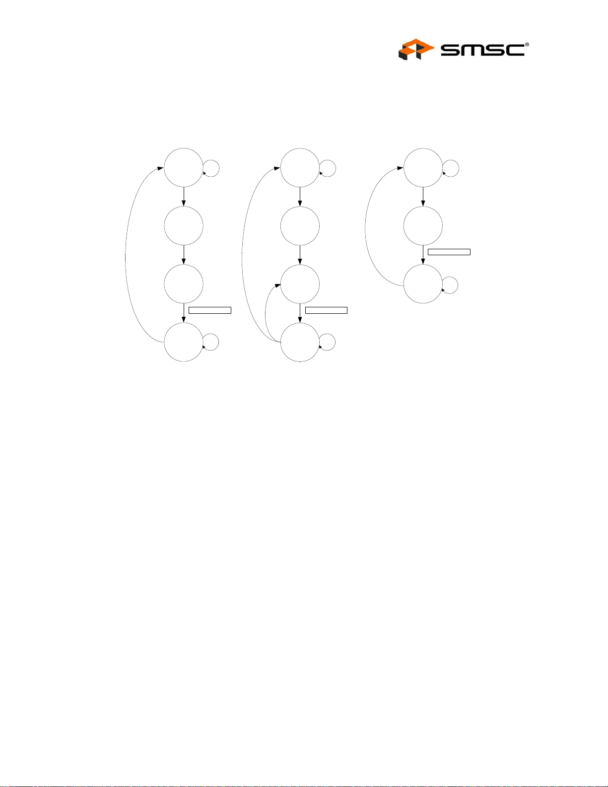
Two Port 10/100 Managed Ethernet Switch with 16-Bit Non-PCI CPU Interface
Datasheet
CSR_BUSY = 0
CSR Write Auto
CSR Write
Increment /
Decrement
Idle
Write Data
Register
Write
Command
Register
min wait period min wait period
Read
Command
Register
CSR_BUSY = 1
CSR_BUSY = 0
Figure 6.1 Switch Fabric CSR Write Access Flow Dia gram
Idle
Write
Command
Register
Write Data
Register
Read
Command
Register
CSR_BUSY = 1
CSR Write Direct
Address
Idle
Write
Direct
Data
Register
Range
min wait period
Read
Command
RegisterCSR_BUSY = 0
CSR_BUSY = 1
6.2.2 Switch Fabric CSR Reads
To perform a read of an individual switch fabric register, the read cycle must be initiated by performing
a single write to the Switch Fabric CSR Interface Command Register (SWITCH_CSR_CMD) with
CSR_BUSY (bit 31) set, the CSR_ADDRESS field (bits 15:0) set to the desired register address, the
R_nW (bit 30) set, and the AUTO_INC and AUTO_DEC fields cleared. Valid data is available for
reading when the CSR_BUSY bit is cleared, indicating that the data can be read fro m the Switch Fabric
CSR Interface Data Register (SWITCH_CSR_DATA).
A second read method may be used which utilizes the auto increment/decrement function of the Switch
Fabric CSR Interface Command Register (SWITCH_CSR_CMD) for reading sequential register
addresses. When using this method, the Switch Fabric CSR Interface Command Register
(SWITCH_CSR_CMD) must first be written with the auto increment(AUTO_INC) or auto
decrement(AUTO_DEC) bit set, the CSR_ADDRESS field written with the desired register address,
and the R_nW bit set. The completion of a read cycle is indicated by the clearing of the CSR_BUSY
bit, at which time the data can be read from the Switch Fabric CSR Interface Data Register
(SWITCH_CSR_DATA). When the data is read, the address in the Switch Fabric CSR Interface
Command Register (SWITCH_CSR_CMD) is incremented or decremented accordingly, and another
read cycle is started automatically. The user should clear the AUTO_INC and AUTO_DEC bits before
reading the last data to avoid an unintended read cycle.
Figure 6.2 illustrates the process required to perform a switch fabric CSR read. The minimum wait
periods as specified in Table 8.1, “Rea d After Write Timing Rules,” on page 103 are required where
noted.
SMSC LAN9311/LAN9311i 57 Revision 1.4 (08-19-08)
DATASHEET
Page 58

Two Port 10/100 Managed Ethernet Switch with 16-Bit Non-PCI CPU Interface
Datasheet
CSR Read Auto
CSR Read
Increment /
Decrement
Idle
Write
Command
Register
min wait period
Read
Command
Register
CSR_BUSY = 0
Read Data
Register
CSR_BUSY = 1
Idle
Write
Command
Register
min wait period min wait period
CSR_BUSY = 1
Read
Command
Register
CSR_BUSY = 0
last
data?
Yes
Write
Command
Register
Read Data
Register
No
Read Data
Register
Figure 6.2 Switch Fabric CSR Read Access Flow Diagram
6.2.3 Flow Control Enable Logic
Each switch fabric port (0,1,2) is provided with two flow control enable inputs per port, one for
transmission and one for reception. Flow control on transmission allows the transmitter to generate
back pressure in half-duplex mode, and pause packets in full-duplex. Flow control in reception enables
the reception of pause packets to pause transmissions.
The state of these enables is based on the state of the ports duplex and Auto-negotiation settings and
the values of the corresponding Manual Flow Control register ( Port 1 Manual Flow Control Register
(MANUAL_FC_1), Port 2 Manual Flow Control Register (MANUAL_FC_2), or Port 0(Host MAC)
Manual Flow Control Register (MANUAL_FC_MII)). Table 6.1 details the switch fabric flow control
enable logic.
When in half-duplex mode, the transmit flow control (back pressure) enabl e is determined directly by
the BP_EN_x bit of the ports manual flow control register. When Auto-negotiation is disabled, or the
MANUAL_FC_x bit of the ports manual flow control register is set, the switch p ort flow control enables
during full-duplex are determined by the TX_FC_x and RX_FC_x bits of the ports manual flow control
Revision 1.4 (08-19-08) 58 SMSC LAN9311/LAN9311i
DATASHEET
Page 59

Two Port 10/100 Managed Ethernet Switch with 16-Bit Non-PCI CPU Interface
Datasheet
register. When Auto-negotiation is enabled and the MANUAL_FC_x bit is cleared, the switch port flow
control enables during full-duplex are determined by Auto-negotiation .
Note: The flow control values in the Port x PHY Auto-Negotiation Advertisement Register
(PHY_AN_ADV_x) and Virtual PHY Auto-Negotiation Advertisement Register
(VPHY_AN_ADV) are not affected by the values of the manual flow control register. Refer to
Section 7.2.5.1, "PHY Pause Flow Control," on page 92 and Section 7.3.1.3, "Virtual PHY
Pause Flow Control," on page 98 for additional information on PHY and Virtual PHY flow
control settings respectively.
Table 6.1 Switch Fabric Flow Control Ena ble Logic
CASE
MANUAL_FC_X
AN ENABLE
AN COMPLETE
LP AN ABLE
-1XXXHalf XXXX0
DUPLEX
AN PAUSE
ADVERTISEMENT
(Note 6.2)
AN ASYM PAUSE
ADVERTISEMENT
(Note 6.2)
LP PAUSE
ABILITY
(Note 6.2)
LP ASYM PAUSE
ABILITY
(Note 6.2)
RX FLOW CONTROL
ENABLE
RX FLOW CONTROL
BP_EN_x
ENABLE
-X0XXHalf XXXX0
-1XXXFull XXXX
-X0XXFull XXXX
101
201
301
401
501
601
701
801
901
10 0 1
11 0 1
0
XX XXXX00
1
0Half (Note 6.1) XXXX0
1
1Half XXXX0
1
1Full 0 0 X X 0 0
1
1Full 0 1 0 X 0 0
1
1Full 011000
1
1Full 011101
1
1Full 1 0 0 X 0 0
1
1Full 1X1X11
1
1Full 110000
1
1Full 110110
RX_FC_x TX_FC_x
RX_FC_x TX_FC_x
Note 6.1 If Auto-negotiation is enabled and complete, but the link partner is not Auto-negotiation
capable, half-duplex is forced via the parallel detect function.
BP_EN_x
BP_EN_x
BP_EN_x
Note 6.2 For the Port 1 and Port 2 PHYs, these are the bits from the Port x PHY Auto-Negotiation
Advertisement Register (PHY_AN_ADV_x) and Port x PHY Auto-Negotiation Link Partner
Base Page Ability Register (PHY_AN_LP_BASE_ABILITY_x). For the Virtual PHY, these
are the local/partner swapped outputs from the bits in the Virtual PHY Auto-Negotiation
Advertisement Register (VPHY_AN_ADV) and Virtual PHY Auto-Negotiation Link Partner
Base Page Ability Register (VPHY_AN_LP_BASE_ABILITY). Refer to Section 7.3.1,
"Virtual PHY Auto-Negotiation," on page 96 for more information.
SMSC LAN9311/LAN9311i 59 Revision 1.4 (08-19-08)
DATASHEET
Page 60

Per Table 6.1, the following cases are possible:
Case 1 - Auto-negotiation is still in progress. Since the result is n ot yet established, flow control is
disabled.
Case 2 - Auto-negotiation is enabled and unsuccessful (lin k partner not Auto-negotiation capable).
The link partner ability is undefined, effectively a don’t-care value, in this case. The duplex setting
will default to half-duplex in this case. Flow control is determined by the BP_ EN_x bit.
Case 3 - Auto-negotiation is enabled and succe ssful with half-duplex as a re sult. The link partner
ability is undefined since it only applies to ful l-duplex operation. Flow control is determined by the
BP_EN_x bit.
Cases 4-11 -Auto-negotiation is enabled and successful with full-duplex as the result. In these
cases, the advertisement registers and the link partner ability controls the RX and TX enables.
These cases match IEEE 802.3 Annex 28B.3.
Cases 4,5,6,8,10 - No flow control enabled
Case 7 - Asymmetric pause towards partner (away from switch port)
Case 9 - Symmetric pause
Case 11 - Asymmetric pause from partner (towards switch port)
6.3 10/100 Ethernet MACs
Two Port 10/100 Managed Ethernet Switch with 16-Bit Non-PCI CPU Interface
Datasheet
The switch fabric contains three 10/100 MAC blocks, one for each switch port (0,1,2). The 10/100 MAC
provides the basic 10/100 Ethernet functionality, including transmission deferral and collision backoff/retry, receive/transmit FCS checking and generation, receive/transmit pause flow control, and
transmit back pressure. The 10/100 MAC also includes RX and TX FIFOs and per port statistic
counters.
6.3.1 Receive MAC
The receive MAC (IEEE 802.3) sublayer decomposes Ethernet packets acquired via the internal MII
interface by stripping off the preamble sequence and Start of Frame Delimiter (SFD). The receive MAC
checks the FCS, the MAC Control Type, and the byte count against the drop conditions. The packet
is stored in the RX FIFO as it is received.
The receive MAC determines the validity of each received packet by checking the Type field, FCS, and
oversize or undersize conditions. All bad packets will be either immediately dropped or ma rked (at the
end) as bad packets.
Oversized packets are normally truncated at 1519 or 1523 (VLAN tagged) octets and marked as
erroneous. The MAC can be configured to accept packets up to 2048 octets (inclusive), in which case
the oversize packets are truncated at 2048 bytes and marked as erroneous.
Undersized packets are defined as packets with a length less than the minimum packet size. The
minimum packet size is defined to be 64 bytes, exclusive of preamble sequence and SFD.
The FCS and length/type fields of the frame is checked to detect if the packet has a valid MAC control
frame. When the MAC receives a MAC control frame with a valid FCS and determines the opera tion
code is a pause command (Flow Control frame), the MAC will load its internal pause counter with the
Number_of_Slots variable from the MAC control frame just received. Anytime the internal pause
counter is zero, the transmit MAC will be allowed to transmit (XON). If the internal pause counter is
not zero, the receive MAC will not allow the transmit MAC to transmit (XOFF). When the transmit MAC
detects an XOFF condition it will continue to transmit the current packet, terminating transmission a fter
the current packet has been transmitted until receiving the XON condition from the receive MAC. The
pause counter will begin to decrement at then end of the current transmission, or immediately if no
transmission is underway. If another pause command is received while the transmitter is already in
pause, the new pause time indicated by the Flow Control packet will be loaded into the pause counter.
The pause function is enabled by either Auto-negotiation, or manually as discussed in Section 6.2.3,
Revision 1.4 (08-19-08) 60 SMSC LAN9311/LAN9311i
DATASHEET
Page 61

Two Port 10/100 Managed Ethernet Switch with 16-Bit Non-PCI CPU Interface
Datasheet
"Flow Control Enable Logic," on page 58. Pause frames are consumed by the MAC and not sent to
the switch engine. Non-pause control frames are optionally filtered o r forwarded.
When the receive FIFO is full and additional data continues to be received, an overrun condition occurs
and the frame is discarded (FIFO space recovered) or marked as a bad frame.
The receive MAC can be disabled from receivin g all frames by clearing the RX Enable bit of the Port
x MAC Receive Configuration Register (MAC_RX_CFG_x).
The size of the RX FIFO is 256 bytes. If a bad packet with less than 64 bytes is received, it will be
flushed from the FIFO automatically and the FIFO space recovered. Packets equal to or larger th an
64 bytes with an error will be marked and reported to the switch engine. The switch engine will
subsequently drop the packet.
6.3.1.1 Receive Counters
The receive MAC gathers statistics on each packet and increments the related counter registers. The
following receive counters are supported for each switch fabric port. Refer to Table 14.12, “Indirectly
Accessible Switch Control and Status Registers,” on page 309 and Section 14.5.2.3 through
Section 14.5.2.22 for detailed descriptions of these counters.
Total undersized packets (Section 14.5.2.3, on page 326)
Total packets 64 bytes in size (Section 14.5.2.4, on page 327)
Total packets 65 through 127 bytes in size (Section 14.5.2.5, on page 328)
Total packets 128 through 255 bytes in size (Section 14.5.2 .6, on page 329)
Total packets 256 through 511 bytes in size (Section 14.5.2.7, on page 330)
Total packets 512 through 1023 bytes in size (Section 14.5.2.8, on page 331 )
Total packets 1024 through maximum bytes in size (Section 14.5.2.9, on page 3 32)
Total oversized packets (Section 14.5.2.10, on page 333)
Total OK packets (Section 14.5.2.11, on page 334)
Total packets with CRC errors (Section 14.5.2 .12, on page 335)
Total multicast packets (Section 14.5.2.13, on page 336)
Total broadcast packets (Section 14.5.2.14, on page 337)
Total MAC Pause packets (Section 14.5.2.15, on page 338)
Total fragment packets (Section 14.5.2.16, on page 33 9)
Total jabber packets (Section 14.5.2.17, on page 34 0)
Total alignment errors (Section 14.5.2.18, on page 341)
Total bytes received from all packets (Section 14.5.2.19, on page 342)
Total bytes received from good packets (Section 14.5.2.20, on page 343)
Total packets with a symbol error (Section 14.5.2.21, on page 344)
Total MAC control packets (Section 14.5.2.22, on page 345)
SMSC LAN9311/LAN9311i 61 Revision 1.4 (08-19-08)
DATASHEET
Page 62

6.3.2 Transmit MAC
The transmit MAC generates an Ethernet MAC frame from TX FIFO data. This includes ge nerating the
preamble and SFD, calculating and appending the frame checksum value, optionally padding
undersize packets to meet the minimum packet requirement size (64 bytes), and maintaining a
standard inter-frame gap time during transmit.
The transmit MAC can operate at 10/100Mbps, half- or full-duplex, and with or without flow control
depending on the state of the transmission. In half-duplex mode the transmit MAC meets CSMA/CD
IEEE 802.3 requirements. The transmit MAC will re-transmit if collisions occur during the first 64 bytes
(normal collisions), or will discard the packet if collisions occur after the first 64 bytes (late collisions).
The transmit MAC follows the standard truncated binary exponential back-off algorithm, collision and
jamming procedures.
The transmit MAC pre-pends the standard preamble and SFD to every packet from the FIFO. The
transmit MAC also follows as default, the standard Inter-Frame Gap (IFG). The default IFG is 96 bit
times and can be adjusted via the IFG Config field of the Port x MAC Transmit Configuration Register
(MAC_TX_CFG_x).
Packet padding and cyclic redundant code (FCS) calculation may be optionally performed by the
transmit MAC. The auto-padding process automatically adds enough zeros to packets shorter than 64
bytes. The auto-padding and FCS generation is controlled via the TX Pad Ena ble bit of the Port x MAC
Transmit Configuration Register (MAC_TX_CFG_x).
Two Port 10/100 Managed Ethernet Switch with 16-Bit Non-PCI CPU Interface
Datasheet
The transmit FIFO acts as a temporary buffer between the transmit MAC and the switch engine . The
FIFO logic manages the re-transmission for normal collision conditions or discards the frames for late
or excessive collisions.
When in full-duplex mode, the transmit MAC uses the flow-control algorithm specified in IEEE 802.3.
MAC pause frames are used primarily for flow control packets, which pass signalling information
between stations. MAC pause frames have a unique type of 8808h, and a pause op-co de of 0001h.
The MAC pause frame contains the pause value in the data field. The flow control manager will autoadapt the procedure based on traffic volume and speed to avoid packet loss and unnecessary pause
periods.
When in half-duplex mode, the MAC uses a back pressure algorithm. The back pressure algorithm is
based on a forced collision and an aggressive back-off algorithm.
6.3.2.1 Transmit Counters
The transmit MAC gathers statistics on each packet and increments the related counter registers. The
following transmit counters are supported for each switch fabric port. Refer to Table 14.12, “Indirectly
Accessible Switch Control and Status Registers,” on page 309 and Section 14.5.2.25 through
Section 14.5.2.42 for detailed descriptions of these counters.
Total packets deferred (Section 14.5.2.25, on page 348)
Total pause packets (Section 14.5.2.26, on page 349)
Total OK packets (Section 14.5.2.27, on page 350)
Total packets 64 bytes in size (Section 14.5.2.28, on page 351)
Total packets 65 through 127 bytes in size (Section 14.5.2.29, on page 352 )
Total packets 128 through 255 bytes in size (Section 14.5.2 .30, on page 353)
Total packets 256 through 511 bytes in size (Section 14.5.2.31, on page 354)
Total packets 512 through 1023 bytes in size (Section 14.5.2.32, on page 355 )
Total packets 1024 through maximum bytes in size (Section 14.5.2.33, on page 356 )
Total undersized packets (Section 14.5.2.34, on page 357)
Total bytes transmitted from all packets (Section 14.5.2.35, on page 358)
Total broadcast packets (Section 14.5.2.36, on page 359)
Revision 1.4 (08-19-08) 62 SMSC LAN9311/LAN9311i
DATASHEET
Page 63

Two Port 10/100 Managed Ethernet Switch with 16-Bit Non-PCI CPU Interface
Datasheet
Total multicast packets (Section 14.5.2.37, on page 360)
Total packets with a late collision (Section 14.5.2.3 8, on page 361)
Total packets with excessive collisions (Section 14.5.2.39, on page 362)
Total packets with a single collision (Section 14.5.2.40, o n page 363)
Total packets with multiple collisions (Section 14.5.2.41, on page 364)
Total collision count (Section 14.5.2.42 , on page 365)
6.4 Switch Engine (SWE)
The switch engine (SWE) is a VLAN layer 2 (link layer) switching engine supporting 3 ports. The SWE
supports the following types of frame formats: untagged frames, VLAN tagged frames, and priority
tagged frames. The SWE supports both the 802.3 and Ethernet II frame formats.
The SWE provides the control for all forwarding/filtering rules. It handles the address learning and
aging, and the destination port resolution based upon the MAC address and VLAN of the packet. The
SWE implements the standard bridge port states for spanning tree and provides packet metering for
input rate control. It also implements port mirroring, broadcast throttling, and multicast pruning and
filtering. Packet priorities are supported based on th e IPv4 TOS bits and IPv6 Traffic Class bits using
a DIFFSERV Table mapping, the non-DIFFSERV mapped IPv4 precedence bits, VLAN priority using
a per port Priority Regeneration Table, DA based static priority, and Traffic Class mapping to one of 4
QoS transmit priority queues.
The following sections detail the various features of the switch engine.
6.4.1 MAC Address Lookup Table
The Address Logic Resolution (ALR) maintains a 1024 entry MAC Addres s Table. The ALR searches
the table for the destination MAC address. If the search finds a match, the associated data is returned
indicating the destination port or ports, whether to filter the packet, the packets priority (used if
enabled), and whether to override the ingress and egress spanning tree port state. Figure 6.3 displays
the ALR table entry structure. Refer to the Switch Engine ALR Write Data 0 Register
(SWE_ALR_WR_DAT_0) and Switch Engine ALR Write Data 1 Register (SWE_ALR_WR_DAT_1) for
detailed descriptions of these bits.
Bit
56
Valid
55
Age /
Override
53
Static54Filter
52 51
Priority
Figure 6.3 ALR Table Entry Structure
50 49 48
Port
47 0
...
MAC Address
SMSC LAN9311/LAN9311i 63 Revision 1.4 (08-19-08)
DATASHEET
Page 64

6.4.1.1 Learning/Aging/Migration
The ALR adds new MAC addresses upon ingress along with the associate d receive port.
If the source MAC address already exists, the entry is refreshed. This action serves two purposes.
First, if the source port has changed due to a network reconfiguration (migration), it is updated.
Second, each instance the entry is refreshed, the aging status bit is set, keeping the entry active.
Learning can be disabled per port via the Enable Learning on Ingress field o f the Switch Engine Port
Ingress Configuration Register (SWE_PORT_INGRSS_CFG).
During each aging period, the ALR scans the learned MAC addresses. For entries which have the
aging status bit set, the ALR simply clears the bit. As mentioned above, if a MAC address is
subsequently refreshed, the aging bit will be se t again and the process woul d repeat. If a le arned entry
already had its aging status bit cleared (by a previous scan), the ALR will instead remove the learned
entry. Therefore, if two scans occur before a MAC address is refreshed, the entry will be aged and
removed. Each aging period is approximately 5 minutes. Therefore an entry will be aged and removed
at a minimum of 5 minutes, and a maximum of 10 minutes.
6.4.1.2 Static Entries
If a MAC address entry is manually added by the host CPU, it can be (and typically is) marked as
static. Static entries are not subjected to the aging process. Static entries also cannot be changed by
the learning process (including migration).
Two Port 10/100 Managed Ethernet Switch with 16-Bit Non-PCI CPU Interface
Datasheet
6.4.1.3 Multicast Pruning
The destination port that is returned as a result of a destination MAC address lookup may be a single
port or any combination of ports. The latter is used to setup multicast address groups. An entry with
a multicast MAC address would be entered manually by the host CPU with the appropriate destination
port(s). Typically, the Static bit should also be set to prevent automatic aging of the entry.
6.4.1.4 Address Filtering
Filtering can be performed on a destination MAC address. Such an entry would be entered manually
by the host CPU with the Filter bit active. Typically, the Static bit should also be set to prevent
automatic aging of the entry.
6.4.1.5 Spanning Tree Port State Override
A special spanning tree port state override setting can be applied to MAC address entries. When the
host CPU manually adds an entry with both the Static and Age bits set, packets with a matching
destination address will bypass the spanning tree port state and will be forwarded. This feature is
typically used to allow the reception of the BPDU packets while a port is in the non-forwarding state.
Refer to Section 6.4.5, "Spanning Tree Support," on page 70 for additional details.
6.4.1.6 MAC Destination Address Lookup Priority
If enabled in the Switch Engine Global Ingress Configuration Register
(SWE_GLOBAL_INGRSS_CFG), the transmit priority for static MAC address entries is taken from the
associated data of that entry.
6.4.1.7 Host Access
The ALR contains a learning engine that is used by the host CPU to add, delete, and modify the MAC
Address Table. This engine is accessed by using the Switch Engine ALR Command Register
(SWE_ALR_CMD), Switch Engine ALR Command Status Register (SWE_ALR_CMD_STS), Switch
Engine ALR Write Data 0 Register (SWE_ALR_WR_DAT_0), and Switch Engine ALR Write Data 1
Register (SWE_ALR_WR_DAT_1).
Revision 1.4 (08-19-08) 64 SMSC LAN9311/LAN9311i
DATASHEET
Page 65

Two Port 10/100 Managed Ethernet Switch with 16-Bit Non-PCI CPU Interface
Datasheet
The following procedure should be followed in order to add, delete, and modify the ALR entries:
1. Write the Switch Eng ine ALR Write Data 0 Register (SWE_ALR_WR_DAT_0) and Switch Engine
ALR Write Data 1 Register (SWE_ALR_WR_DAT_1) with the desired MAC address and control
bits.
Note:An entry can be deleted by setting the Valid and Static bits to 0.
2. Write the Switch Engine ALR Command Register (SWE_ALR_CMD) register with 0004h (Make
Entry)
3. Poll the Make Pending bit in the Switch Engine ALR Command Status Register
(SWE_ALR_CMD_STS) until it is cleared.
4. Write the Switch Engine ALR Command Register (SWE_ALR_CMD) with 0000h.
The ALR contains a search engine that is used by the host to read the MAC Address Table. This
engine is accessed by using the Switch Engine ALR Command Register (SWE_ALR_CMD), Switch
Engine ALR Read Data 0 Register (SWE_ALR_RD_DAT_0), and Switch Engine ALR Read Data 1
Register (SWE_ALR_RD_DAT_1).
Note: The entries read are not necessarily in the same order as they were learned or manually
added.
The following procedure should be followed in order to read the ALR entries:
1. Write the Switch Engine ALR Command Register (SWE_ALR_CMD) with 0002h (Get First Entry).
2. Write the Switch Engine ALR Command Register (SWE_ALR_CMD) with 0000h (Clear the Get
First Entry Bit)
3. Poll the Valid and End of Table bits in the Switch Engine ALR Read Data 1 Register
(SWE_ALR_RD_DAT_1) until either are set.
4. If the Valid bit is set, then the entry is valid and the data from the Switch Engine ALR Read Data
0 Register (SWE_ALR_RD_DAT_0) and Switch Engine ALR Read Data 1 Register
(SWE_ALR_RD_DAT_1) can be stored.
5. If the End of Table bit is set, then exit.
6. Write the Switch Engine ALR Command Register (SWE_ALR_CMD) with 0001h (Get Next Entry).
7. Write the Switch Engine ALR Command Register (SWE_ALR_CMD) with 0000h (Clear the Get
Next Entry bit)
8. Go to step 3.
Note: Refer to Section 14.5.3.1, on page 368 through Section 14.5.3.6, on page 375 for detailed
definitions of these registers.
SMSC LAN9311/LAN9311i 65 Revision 1.4 (08-19-08)
DATASHEET
Page 66

6.4.2 Forwarding Rules
Upon ingress, packets are filtered or forwarded based on the following rules:
If the destination port equals the source port (local traffic), the packet is filtered.
If the source port is not in the forwarding state, the packet is filtered (unless the Spanning Tree
Port State Override is in effect).
If the destination port is not in the forwarding state, the packet is filtered (unless the Spanning Tree
Port State Override is in effect).
If the Filter bit for the Destination Address is set in the AL R table, the packet is filtered.
If the packet has a unicast destination MAC address which is not found in the ALR table and the
Drop Unknown bit is set, the packet is filtered.
If the packet has a multicast destination MAC address which is not found in the ALR table and the
Filter Multicast bit is set, the packet is filtered.
If the packet has a broadcast destination MAC address and the Broadcast Storm Control level has
been reached, the packet is discarded.
If Drop on Yellow is set, the packet is colored Yellow, and randomly selected, it is discarded.
If Drop on Red is set and the packet is colored Red, it is discarded.
If the destination address was not found in the ALR table (an unknown or a broadcast) and th e
Broadcast Buffer Level is exceeded, the packet is discarded.
If there is insufficient buffer space, the packet is discarded.
Two Port 10/100 Managed Ethernet Switch with 16-Bit Non-PCI CPU Interface
Datasheet
When the switch is enabled for VLAN support, these following ru les also apply:
If the packet is untagged or priority tagged and the Admit Only VLAN bit for the ingress port is set,
the packet is filtered.
If the packet is tagged and has a VID equal to FFFh, it is filtered.
If Enable Membership Checking on Ingress is set, Admit Non Member is cleared, and the source
port is not a member of the incoming VLAN, the packet is filtered.
If Enable Membership Checking on Ingress is set and the destination port is not a member of the
incoming VLAN, the packet is filtered.
If the destination address was not found in the AL R table (as unknown or broadcast) and the VLAN
broadcast domain containment resulted in zero valid destination ports, the packet is filtered.
Note: For the last th ree cases, if the VID is not in the VLAN table, the VLAN is considered foreign
and the membership result is NULL. A NULL membership will result in the packet being filtered
if Enable Membership Checking is set. A NULL membership will also resu lt in the packet being
filtered if the destination address is not found in the ALR table (since the packet would have
no destinations).
Revision 1.4 (08-19-08) 66 SMSC LAN9311/LAN9311i
DATASHEET
Page 67
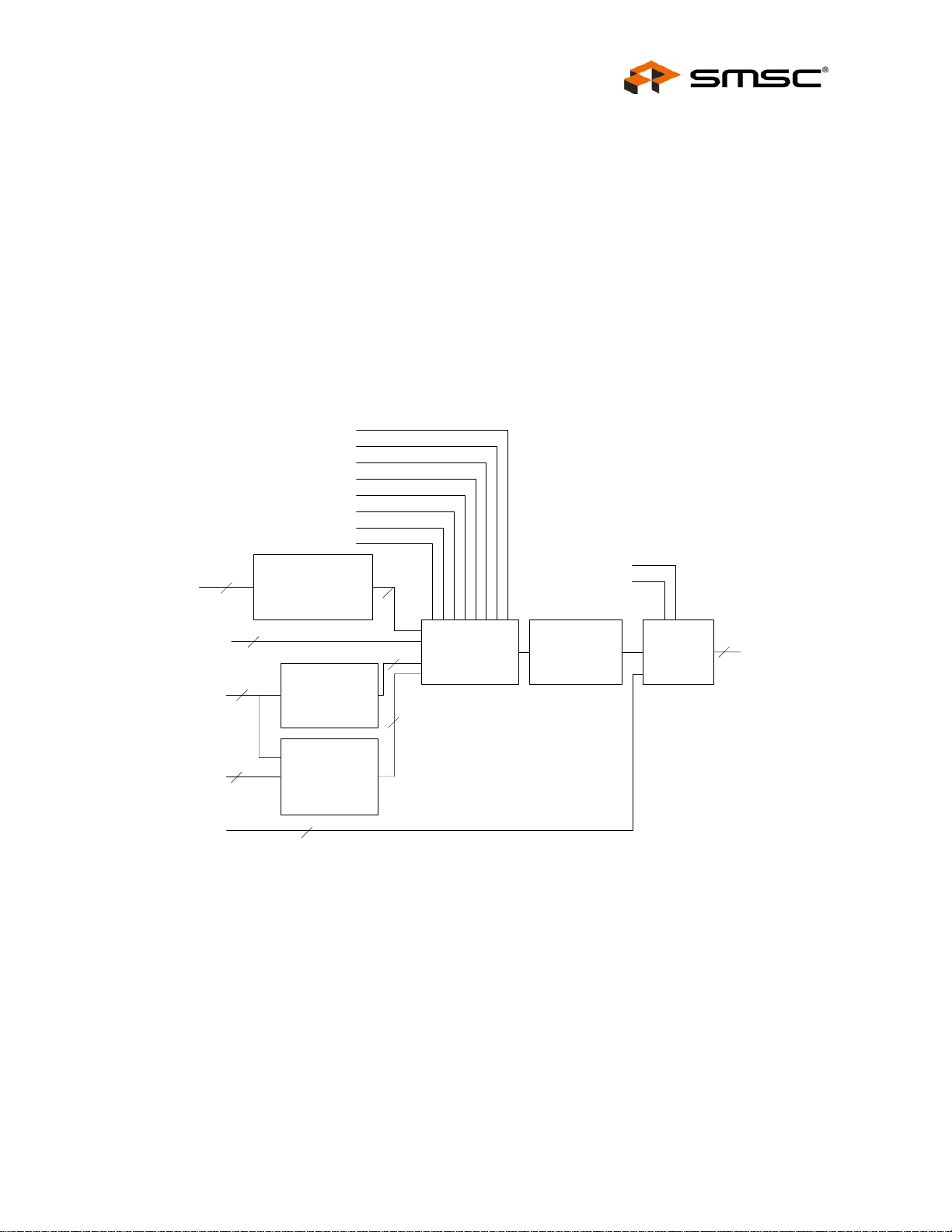
Two Port 10/100 Managed Ethernet Switch with 16-Bit Non-PCI CPU Interface
Datasheet
6.4.3 Transmit Priority Queue Selection
The transmit priority queue may be selected from five options. As shown in Figure 6.4, the priority may
be based on:
the static value for the destination address in the ALR table
the precedence bits in the IPv4 TOS octet
the DIFFSERV mapping table indexed by the IPv4 TOS octet or the IPv6 Traffic Class octet
the VLAN tag priority field using the per port Priority Regeneration table
the port default
The last four options listed are sent through the Traffic Class table which maps the selected priority to
one of the four output queues. The static value from the ALR table directly specifies the queue.
Packet is from Host
Packet is Tagged
Packet is IPv4
Packet is IP
VL Higher Priority
Use Precedence
Use IP
VLAN Enable
IPv4(TOS)
IPv6(TC)
6b
programmable
DIFFSERV table
3b
ALR Static Bit
DA Highest Priority
IPv4 Precedence
Source Port
VLAN Priority
ALR Priority
3b
3b
2b
programmable
Traffic Class
table
programmable
port default
table
programmable
Priority
Regeneration
table
per port
2b
3b
3b
priority
cal culation
Figure 6.4 Switch Engine Transmit Queue Selection
static DA
override
2b
priority queue
SMSC LAN9311/LAN9311i 67 Revision 1.4 (08-19-08)
DATASHEET
Page 68
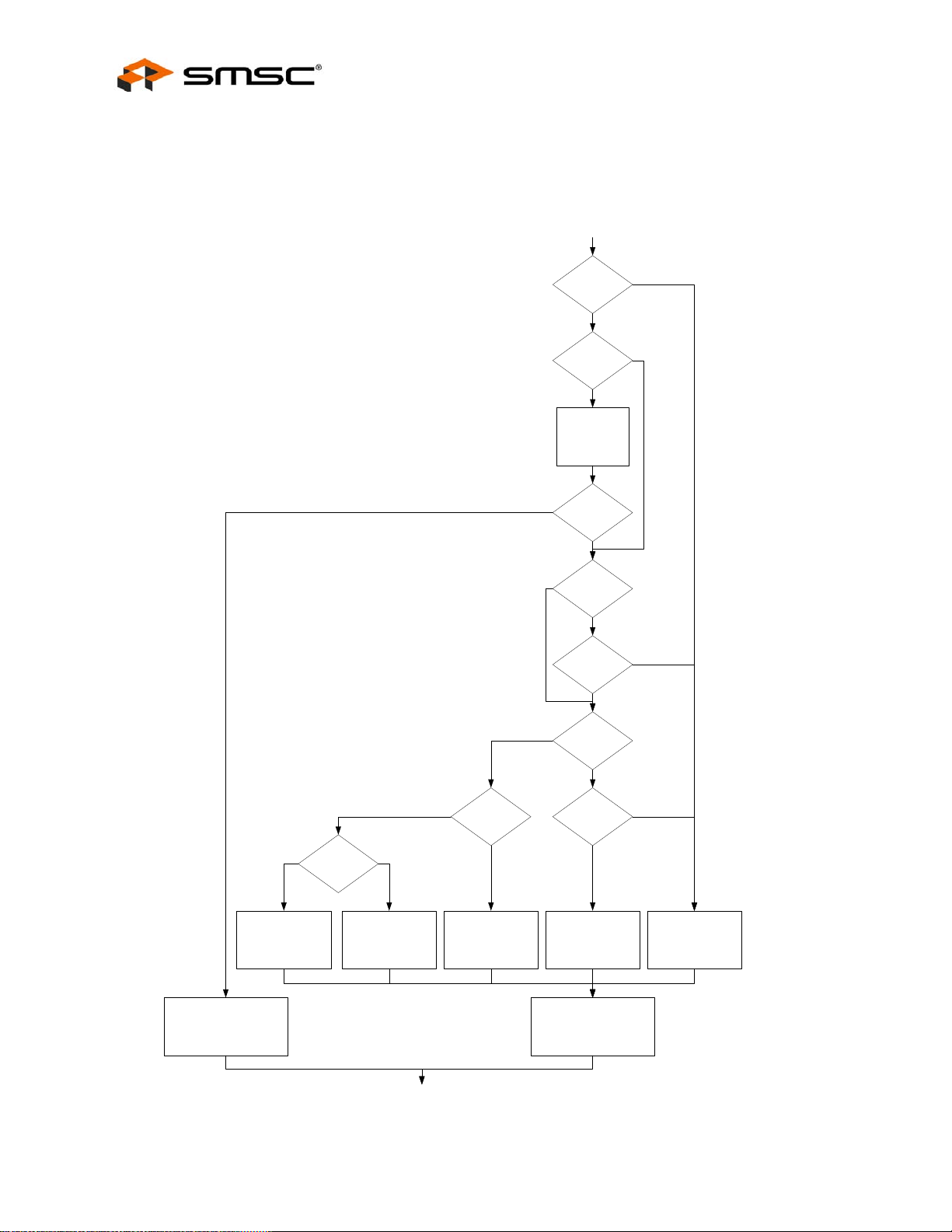
Two Port 10/100 Managed Ethernet Switch with 16-Bit Non-PCI CPU Interface
Datasheet
The transmit queue priority is based on the packet type and device configuration as shown in
Figure 6.5. Refer to Section 14.5.3.16, "Switch Engine Global Ingress Configuration Register
(SWE_GLOBAL_INGRSS_CFG)," on page 385 for defi nitions of the configuration bits.
Get Queue
Packet from Host
DA Highest
Priority
wait for ALR result
Y
ALR Static Bit
N
VL Higher
Priority
VLAN Enable &
Packet is
Tagged
Y
N
N
Y
N
Y
Y
N
Y
Packet is IPv4/v6
& Use IP
N
VLAN Enable &
Packet is
Tagged
Resolved Priorit y =
Default Priority[Source
Port]
Queue =
Traffic Class[Resolved Priority]
Y
N
Resolved P riority =
Priority Regen[VLAN
Priority]
Queue =
ALR Priority
Y N
Resolved Priority =
IP Precedence
Use Precedence
Resolved Priorit y =
DIFFSERV[TOS]
Get Queue Done
Y
Packet is IPv4
N
Resolved Priority =
DIFFSERV[TC]
Figure 6.5 Switch Engine Transmit Queue Calculation
Revision 1.4 (08-19-08) 68 SMSC LAN9311/LAN9311i
DATASHEET
Page 69

Two Port 10/100 Managed Ethernet Switch with 16-Bit Non-PCI CPU Interface
Datasheet
6.4.3.1 Port Default Priority
As detailed in Figure 6.5, the default priority is based on the ingr ess ports priority bits in its port VID
value. The PVID table is read and written by using the Switch Engine VLAN Command Register
(SWE_VLAN_CMD), Switch Engine VLAN Write Data Register (SWE_VLAN_WR_DATA), Switch
Engine VLAN Read Data Register (SWE_VLAN_RD_DATA), and Switch Engine VLAN Command
Status Register (SWE_VLAN_CMD_STS). Refer to Section 14.5.3.8, on page 377 through Section
14.5.3.11, on page 380 for detailed VLAN register descriptions.
6.4.3.2 IP Precedence Based Priority
The transmit priority queue can be chosen based on the Precedence bits of the IPv4 TOS octet. This
is supported for tagged and non-tagged packets for both type field and length field encapsulations. The
Precedence bits are the three most significant bits of the IPv4 TOS octet.
6.4.3.3 DIFFSERV Based Priority
The transmit priority queue can be chosen based on th e DIFFSERV usage of the IPv4 TOS or IPv6
Traffic Class octet. This is supported for tagged and non-tagged packets for both type field and length
field encapsulations.
The DIFFSERV table is used to determine the packet priority from the 6-bit Differentiated Services (DS)
field. The DS field is defined as the six most significant bits of the IPv4 TOS octet or the IPv6 Traffic
Class octet and is used as an index into the DIFF SERV table. The output of the DIFFSERV table is
then used as the priority. This priority is then passed through the Traffic Class table to select the
transmit priority queue.
Note: The DIFF SERV table is not initialized upon reset or power-up. If DIFFSERV is enabled, then
the full table must be initialized by the host.
The DIFFSERV table is read and written by using the Switch Engine DIFFSERV Table Command
Register (SWE_DIFFSERV_TBL_CFG), Switch Engine DIFFSERV Table Write Data Register
(SWE_DIFFSERV_TBL_WR_DATA), Switch Engine DIFFSERV Table Read Data Register
(SWE_DIFFSERV_TBL_RD_DATA), and Switch Engine DIFFSERV Table Command Status Register
(SWE_DIFFSERV_TBL_CMD_STS). Refer to Section 14.5.3.12, on page 381 through Section
14.5.3.15, on page 384 for detailed DIFFSERV register descriptions.
6.4.3.4 VLAN Priority
As detailed in Figure 6.5, the transmit priori ty queue can be taken from the priority field of the VLAN
tag. The VLAN priority is sent through a per port Priority Regeneration table, which is used to map the
VLAN priority into a user defined priority.
The Priority Regeneration table is programmed by using the Switch Engine Port 0 Ingress VLAN
Priority Regeneration Table Register (SWE_INGRSS_REGEN_TBL_MII), Switch Engine Port 1 Ingress
VLAN Priority Regeneration Table Register (SWE_INGRSS_REGEN _TBL_1), and Switch Engine Port
2 Ingress VLAN Priority Regeneration Table Register (SWE_INGRSS_REGEN_TBL_2). Refer to
Section 14.5.3.33, on page 404 through Section 14.5.3.35, on page 406 for detailed descriptions of
these registers.
SMSC LAN9311/LAN9311i 69 Revision 1.4 (08-19-08)
DATASHEET
Page 70

6.4.4 VLAN Support
The switch engine supports 16 active VLANs out of a possible 4096. The VLAN table contains th e 16
active VLAN entries, each consisting of the VID, the port membership, and un-tagging instructions.
Two Port 10/100 Managed Ethernet Switch with 16-Bit Non-PCI CPU Interface
Datasheet
17 16 15 14 13 12
Member
Port 2
On ingress, if a packet has a VLAN tag containing a valid VID (not 000h or FFFh), the VID table is
searched. If the VID is found, the VLAN is considered active and the membership and un-tag
instruction is used. If the VID is not found, the VLAN is considered foreign and the membership result
is NULL. A NULL membership will result in the packet being filtered if Enable Membership Checking
is set. A NULL membership will also result in the packet being filtered if the destination address is not
found in the ALR table (since the packet would have no destinations).
On ingress, if a packet does not have a VLAN tag or if the VLAN tag contains VID with a value of 0
(priority tag), the packet is assigned a VLAN based on the Port Default VID (PVID) and Priority. The
PVID is then used to access the above VLAN table.
The VLAN membership of the packet is used for ingress and egress checking and for VLAN broadca st
domain containment. The un-tag instructions are used at egress on ports defined as hybrid ports.
Refer to Section 14.5.3.8, on page 377 through Section 14.5.3.11, on page 380 for detailed VLAN
register descriptions.
Un-tag
Port 2
Member
Port 1
Un-tag
Port 1
Figure 6.6 VLAN Table Entry Structure
6.4.5 Spanning Tree Support
Member
MII
Un-tag
MII
11 0
...
VID
Hardware support for the Spanning Tree Protocol (STP) and the Rapid Spanning Tree Protocol (RSTP)
includes a per port state register as well as the override bit in the MAC Address Table entries (Section
6.4.1.5, on page 64) and the host CPU port special tagging (Sectio n 6.4.10, on page 75).
The Switch Engine Port State Register (SWE_PORT_STATE) is used to place a port into one of the
modes as shown in Table 6.2. Normally only Port 1 and Port 2 are placed into modes other than
forwarding. Port 0 should normally be left in forwarding mode.
Table 6.2 Spanning Tree States
Port State Hardware Action Software Action
01 - Blocking
(also used for
disabled)
Received packets on the port are
discarded.
Transmissions to the port are blocked.
Learning on the port is disabled.
The MAC Address Table should be programmed
with entries that the host CPU needs to receive
(e.g. the BPDU address). The static and override
bits should be set.
The host CPU should not send any packets to the
port in this state.
The host CPU should discard received packets
from this port when in the Disabled state.
Note: There is no hardware distinction between
the Blocking and Disabled states.
Revision 1.4 (08-19-08) 70 SMSC LAN9311/LAN9311i
DATASHEET
Page 71

Two Port 10/100 Managed Ethernet Switch with 16-Bit Non-PCI CPU Interface
Datasheet
T able 6.2 Spanning Tree S tates (continued)
Port State Hardware Action Software Action
11 - Listening Received packets on the port are
discarded.
Transmissions to the port are blocked.
Learning on the port is disabled.
10 - Learning Received packets on the port are
discarded.
Transmissions to the port are blocked.
Learning on the port is enabled.
00 - Forwarding Received packets on the port are
forwarded normally.
Transmissions to the port are sent
normally.
Learning on the port is enabled.
The MAC Address Table should be programmed
with entries that the host CPU needs to receive
(e.g. the BPDU address). The static and override
bits should be set.
The host CPU may send packets to the port in this
state.
The MAC Address Table should be programmed
with entries that the host CPU needs to receive
(e.g. the BPDU address). The static and override
bits should be set.
The host CPU may send packets to the port in this
state.
The MAC Address Table should be programmed
with entries that the host CPU needs to receive
(e.g. the BPDU address). The static and override
bits should be set.
The host CPU may send packets to the port in this
state.
6.4.6 Ingress Flow Metering and Coloring
The LAN9311/LAN9311i supports hardware ingress rate limiting by metering packet streams and
marking packets as either Green, Yellow, or Red according to three traffic parameters: Committed
Information Rate (CIR), Committed Burst Size (CBS), and Excess Burst Size (EBS). A packet is
marked Green if it does not exceed the CBS, Yellow if it exceeds to CBS but not the EBS, or Red
otherwise.
Ingress flow metering and coloring is enabled via the Ingress Rate Enable bit in the Switch Engine
Ingress Rate Configuration Register (SWE_INGRSS_RATE_CFG). Once enabled, each incoming
packet is classified into a stream. Streams are defined as per port (3 streams), per priority (8 streams),
or per port & priority (24 streams) as selected via the Rate Mode bits in the Switch Engine Ingress
Rate Configuration Register (SWE_INGRSS_RATE_CFG). Each stream can have a different CIR
setting. All streams share common CBS and EBS settings. CIR, CBS, and EBS are programmed via
the Switch Engine Ingress Rate Command Register (SWE_INGRSS_RATE_CMD) and Switch Engine
Ingress Rate Write Data Register (SWE_INGRSS_RATE_WR_DATA).
Each stream is metered according to RFC 2697. At the rate set by the CIR, two token buckets are
credited per stream. First, the Committed Burst bucket is incremented up to the maximum set by the
CBS. Once the Committed Burst bucket is full, the Excess Burst bucket is incremented up to the
maximum set by the EBS. The CIR rate is specified in time per byte. The value programmed is in
approximately 20 nS per byte increments. Typical values are listed in Table 6.3. When a port is
receiving at 10Mbps, any setting faster than 39 has the effect of not limiting the rate.
SMSC LAN9311/LAN9311i 71 Revision 1.4 (08-19-08)
DATASHEET
Page 72

Two Port 10/100 Managed Ethernet Switch with 16-Bit Non-PCI CPU Interface
Table 6.3 Typical Ingress Rate Settings
CIR Setting Time Per Byte Bandwidth
0-3 80 nS 100 Mbps
4 100 nS 80 Mbps
5 120 nS 67 Mbps
6 140 nS 57 Mbps
7 160 nS 50 Mbps
9 200 nS 40 Mbps
12 260 nS 31 Mbps
19 400 nS 20 Mbps
39 800 nS 10 Mbps
79 1600 nS 5 Mbps
160 3220 nS 2.5 Mbps
Datasheet
402 8060 nS 1 Mbps
804 16100 nS 500 Kbps
1610 32220 nS 250 Kbps
4028 80580 nS 100 Kbps
8056 161140 nS 50 Kbps
After each packet is received, the bucket is decremented. If the Committed Burst bucket has sufficient
tokens, it is debited and the packet is colored Green. If the Committed Burst bucket lacks sufficient
tokens for the packet, the Excess Burst bucket is checked. If the Excess Burst bucket has sufficient
tokens, it is debited, the packet is colored Yellow and is subjecte d to random discard. If the Excess
Burst bucket lacks sufficient tokens for the packet, the packet is colored Red and is discarded.
Note: All of the token buckets are initialized to the default value of 1536. If lower values are
programmed into the CBS and EBS parameters, the token buckets will need to be normally
depleted below these values before the values have any affect on limiting the maximum val ue
of the token buckets.
Refer to Section 14.5.3.25, on page 395 through Section 1 4.5.3.29, on page 400 for detailed register
descriptions.
6.4.6.1 Ingress Flow Calculation
Based on the flow monitoring mode, an ingress flow definition ca n include the ingress priority. This is
calculated similarly to the transmit queue with the exception that the Priority Regeneration and the
Traffic Class table are not used. As shown in Figure 6.7, the priority can be based on:
The precedence bits in the IPv4 TOS octet
The DIFFSERV mapping table indexed by the IPv4 TOS octet or the IPv6 Traffic Class octet
The VLAN tag priority field (but not through the per port Priority Regenerati on table)
The port default
Revision 1.4 (08-19-08) 72 SMSC LAN9311/LAN9311i
DATASHEET
Page 73
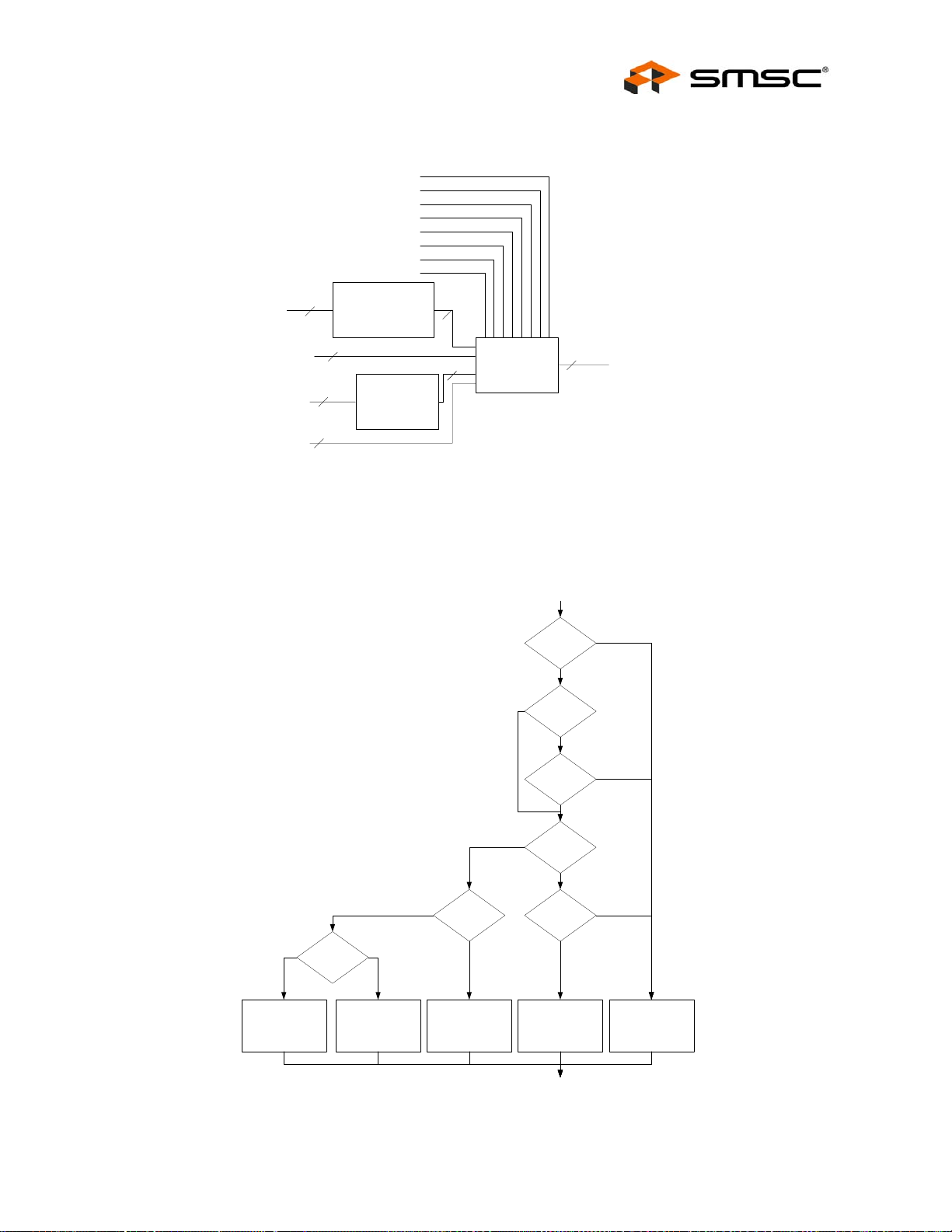
Two Port 10/100 Managed Ethernet Switch with 16-Bit Non-PCI CPU Interface
Datasheet
Packet is from Host
Packet is Tagged
Packet is IPv4
Packet is IP
VL Higher Priority
Use Precedence
Use IP
VLAN Enable
IPv4(TOS)
IPv6(TC)
IPv4 Precedence
Source Port
VLAN Priority
6b
Programmable
DIFFSERV Table
3b
2b
3b
Programmable
Port Default
Table
3b
3b
Priority
Calculation
3b
flow priority
Figure 6.7 Switch Engine Ingr ess Flow Priority Selection
The ingress flow calculation is based on the packet type and the device configuration as shown in
Figure 6.8.
Get Flow Priority
Packet from Host
N
VL Higher
Priority
Y
N
Y
Y N
Flow Priority =
IP Precedence
Use Precedence
Flow Priority =
DIFFSERV[TOS]
Y
Packet is IPv4
Flow Priority =
DIFFSERV[TC]
Vlan Enable &
Packet is
Tagged
Y
Packet is IPv4/v6
& Use IP
Vlan Enable &
Packet is
Tagged
N
Flow Priority =
Default Priority[Source
Get Flow Priority Done
Port]
Y
N
N
Y
N
Flow Priorit y =
VLAN Priority
Figure 6.8 Switch Engine Ingress Flow Priority Calculation
SMSC LAN9311/LAN9311i 73 Revision 1.4 (08-19-08)
DATASHEET
Page 74

6.4.7 Broadcast Storm Control
In addition to ingress rate limiting, the LAN9311/LAN9311i supports hardware broadcast storm control
on a per port basis. This feature is enabled via the Switch Engine Broadcast Throttling Register
(SWE_BCST_THROT). The allowed rate per port is specified as the number of bytes multiplied by 64
allowed to be received every 1.72 mS interval. Packets that exceed this limit are dropped. Typical
values are listed in Table 6.4. Whe n a port is receiving at 10Mbps, any setting above 34 has the e ffect
of not limiting the rate.
Table 6.4 Typical Broadcast Rate Settings
Broadcast Throttle Level Bandwidth
252 75 Mbps
168 50 Mbps
134 40 Mbps
67 20 Mbps
34 10 Mbps
17 5 Mbps
Two Port 10/100 Managed Ethernet Switch with 16-Bit Non-PCI CPU Interface
Datasheet
82.4 Mbps
41.2 Mbps
3 900 Kbps
2 600 Kbps
1 300 Kbps
In addition to the rate limit, the Buffer Manager Broadcast Buffer Level Register (BM_BCST_LVL)
specifies the maximum number of buffers that can be used by broadcasts, multicasts, and unknown
unicasts.
6.4.8 IPv4 IGMP / IPv6 MLD Support
The LAN9311/LAN9311i provides Internet Group Management Protocol (IGMP) and Mul ticast Listener
Discovery (MLD) hardware support using two mechanisms: IGMP/MLD snooping and Multicast
Pruning.
On ingress, if IGMP packet snooping is enabled in the Switch Engine Global Ingress Configuration
Register (SWE_GLOBAL_INGRSS_CFG), IGMP multicast packets are trapped and redirected to the
MLD/IGMP snoop port (typically set to the port to which the host CPU is connected). IGMP packets
are identified as IPv4 packets with a protocol of 2. Both Ethernet and IEEE 802.3 frame formats are
supported as are VLAN tagged packets.
On ingress, if MLD packet snooping is enabled in the Switch Engine Global Ingress Configuration
Register (SWE_GLOBAL_INGRSS_CFG), MLD multicast packets are trapped and redirected to the
MLD/IGMP snoop port (typically set to the port to which the host CPU is connected). MLD packets are
identified as IPv6 packets with a next header value of 58 decimal (ICMPv6). Both Ethernet and IEEE
802.3 frame formats are supported as are VLAN tagged packets.
Once the IGMP or MLD packets are received by the host CPU, the host software can decide which
port or ports need to be members of the multicast group. This group is then added to the ALR table
as detailed in Section 6.4.1.3, "Multicast Pruning," on page 64. The host software should also fo rward
the original IGMP packet if necessary.
Revision 1.4 (08-19-08) 74 SMSC LAN9311/LAN9311i
DATASHEET
Page 75

Two Port 10/100 Managed Ethernet Switch with 16-Bit Non-PCI CPU Interface
Datasheet
Normally, packets are never transmitted back to the receiving port. F or IGMP/MLD snooping, this may
optionally be enabled via the Switch Engine Global Ingress Configuration Register
(SWE_GLOBAL_INGRSS_CFG). This function would be used if the snooping port wished to participate
in the IGMP/MLD group without the need to perform special handling in the transmit portion of the
driver software.
Note: Most forwarding rules are skipped whe n a packet is snooped. However, a packet is still filtered
if:
The source port is not in the forwarding state (unl ess Spanning Tree Port State Override is in
effect.
VLAN’s are enabled, the packet is untagged or priority tagged, and the Admit Only VLAN bit
for the ingress port is set.
VLAN’s are enabled and the packet is tagged and had a VID equal to FFFh.
VLAN’s are enabled, Enabled Membership Checking on Ingress is set, Admit Non Member is
cleared, and the source port is not a member of the incoming VLAN.
6.4.9 Port Mirroring
The LAN9311/LAN9311i supports port mirroring where packets received or transmitted on a port or
ports can also be copied onto another “sniffer” port.
Port mirroring is configured using the Switch Engine Port Mirroring Register (SWE_PORT_MIRROR).
Multiple mirrored ports can be defined, but only one sniffer port can be defined.
When receive mirroring is enabled, packets that are forwarded from a port designated as a mirrored
port are also transmitted by the sniffer port. For example, Port 2 is setup to be a mirrored port and
Port 0 is setup to be the sniffer port. If a packet is received on Port 2 with a destination of Port 1, it
is forwarded to both Port 1 and Port 0.
When transmit mirroring is enabled, packets that are fo rwarded to a port desig nated as a mirrored po rt
are also transmitted by the sniffer port. For example, Port 2 is setup to be a mirrored port and Port 0
is setup to be the sniffer port. If a packet is received on Port 1 with a destination of Port 2, it is
forwarded to both Port 2 and Port 0.
Note: A packet will never be transmitted out of the receiving port. A receive packet is not normally
mirrored if it is filtered. This can optionally be enabled.
6.4.10 Host CPU Port Special Tagging
The Switch Engine Ingress Port Type Register (SWE_INGRSS_PORT_TYP) and Buffer Manager
Egress Port Type Register (BM_EGRSS_PORT_TYPE) are used to enable a special VLAN tag that is
used by the host CPU. This special tag is used to specify the port(s) where packets from the CPU
should be sent, and to indicate which port received the packet that was forwarded to the CPU.
6.4.10.1 Packets from the Host CPU
The Switch Engine Ingress Port Type Register (SWE_INGRSS_PORT_TYP) configures the switch to
use the special VLAN tag in packets from the host CPU as a destination port indicator. A setting of
11b should be u sed on the port that is connected to the host CPU (typically Port 0). A setting of 00b
should be used on the normal network ports.
The special VLAN tag is a normal VLAN tag where the VID field is used as the destination port
indicator. If VID bit 3 is zero, then bits 0 and 1 specify the destination port (0, 1, 2) or broadcast (3 ).
If VID bit 3 is one, then the normal ALR lookup is performed and learning is performed on the source
address. The PRI field from the VLAN tag is used as the packet priority.
Upon egress from the destination port(s), the special tag is removed. If a regular VLAN tag needs to
be sent as part of the packet, then it should be part of the packet data from the host CPU port or set
as an unused bit in the VID field.
SMSC LAN9311/LAN9311i 75 Revision 1.4 (08-19-08)
DATASHEET
Page 76

Note: When sp ecifying Port 0 as the destination port, the VID w ill be set to 0. A VID of 0 is normally
considered a priority tagged packet. Such a packet will be filtered if Admit Only VLAN is set
on the host CPU port. Either avoid setting Admit Only VLAN on the host CPU port or set an
unused bit in the VID field.
Note: The maximu m size tagged packet that can normally be sent into a switch port (from the Host
MAC) is 1522 bytes. Since the special tag consumes four bytes of the packet length, the
outgoing packet is limited to 1518 bytes, even if it contains a regular VLAN tag as part of the
packet data. If a larger outgoing packet is required, the Jumbo2K bit in the Port x MAC Receive
Configuration Register (MAC_RX_CFG_x) of Port 0 should be set.
6.4.10.2 Packets to the Host CPU
The Buffer Manager Egress Port Type Register (BM_EGRSS_PORT_TYPE) configures the switch to
add the special VLAN tag in packets to the host CPU as a source port indicator. A setting of 11b should
be used only on the port that is connected to the host CPU (typically Port 0). Other settings can be
used on the normal network ports as needed.
The special VLAN tag is a normal VLAN tag where bits 0 and 1 of the VID field specify the source
port (0, 1, or 2).
Upon egress from the host CPU port, the special tag is added. If a regular VLAN tag already exists,
it is not deleted. Instead it will follow the sp ecial tag.
Two Port 10/100 Managed Ethernet Switch with 16-Bit Non-PCI CPU Interface
Datasheet
Note: Since the special tag adds four bytes to the length of the packet, it is possible for a normally
tagged, maximum size, incoming packet to become 1526 bytes in length. In order for the Host
MAC to receive this length packet without indicating a length error, the Host MAC VLAN2 Tag
Register (HMAC_VLAN2) in the Host MAC should be set to 8100h and the Host MAC VLAN1
Tag Register (HMAC_VLAN1) should be set to a value o ther than 8100h. This configuration
will allow frames up to 1538 bytes in length to be received.
Note: Since the special tag adds four bytes to the length of the packet, it is possible for a normally
tagged, maximum size, incoming jumbo packet to become 2052 bytes in length. This packet
will be received by the Host MAC with the following conditions:
The receive status will indicate Frame Too Long
Up to four bytes of the end of packet may be truncated (the maximum receive length at the
Host MAC is 2048).
6.4.11 Counters
A counter is maintained per port that contains the number of MAC address that were not learned or
were overwritten by a different address due to MAC Address Table space limitations. These counters
are accessible via the following registers:
Switch Engine Port 0 Learn Discard Count Register (SWE_LRN_DISCRD_CNT_MII)
Switch Engine Port 1 Learn Discard Count Register (SWE_LRN_DISCRD_CNT_1)
Switch Engine Port 2 Learn Discard Count Register (SWE_LRN_DISCRD_CNT_2)
A counter is maintained per port that contains the number of packets filtered at ingress. This count
includes packets filtered due to broadcast throttling, but does not include packets dropped due to
ingress rate limiting. These counters are accessible via the following re gisters:
Switch Engine Port 0 Ingress Filtered Count Register (SWE_FILTERED_CNT_MII)
Switch Engine Port 1 Ingress Filtered Count Register (SWE_FILTERED_CNT_1)
Switch Engine Port 2 Ingress Filtered Count Register (SWE_FILTERED_CNT_2)
Revision 1.4 (08-19-08) 76 SMSC LAN9311/LAN9311i
DATASHEET
Page 77

Two Port 10/100 Managed Ethernet Switch with 16-Bit Non-PCI CPU Interface
Datasheet
6.5 Buffer Manager (BM)
The buffer manager (BM) provides control of the free buffer space, the multiple priority transmit
queues, transmission scheduling, and packet dropping. VLAN tag insertion and removal is also
performed by the buffer manager. The following sections detail the various features of the buffer
manager.
6.5.1 Packet Buffer Allocation
The packet buffer consists of 32KB of RAM that is dynamically allocated in 128 byte blocks as packets
are received. Up to 16 blocks may be used per packet, depending on the packet length. The blocks
are linked together as the packet is received. If a packet is filtered, dropped, or contains a receive
error, the buffers are reclaimed.
6.5.1.1 Buffer Limits and Flow Control Levels
The BM keeps track of the amount of buffers used per each ingress port. These counts are used to
generate flow control (half-duplex backpressure or full-duplex pause frames) and to limit th e amount
of buffer space that can be used by any individual receiver (hard drop limit). The flow control and drop
limit thresholds are dynamic and adapt based on the current buffer usage. Based on the number of
active receiving ports, the drop level and flow control pause and resume thresholds adjust between
fixed settings and two user programmable levels via the Buffer Manager Drop Level Register
(BM_DROP_LVL), Buffer Manager Flow Control Pause Level Register (BM_FC_PAUSE_LVL), and
Buffer Manager Flow Control Resume Level Register (BM_FC_RESUME_LVL) respectively.
The BM also keeps a count of the number of buffers that are queued for multiple ports (broadcast
queue). This count is compared against the Buffer Manager Broadcast Buffer Level Register
(BM_BCST_LVL), and if the configured drop level is reached or exceeded, subsequent packets are
dropped.
6.5.2 Random Early Discard (RED)
Based on the ingress flow monitoring detailed in Section 6.4.6, "Ingress Flow Meterin g and Coloring,"
on page 71, packets are colored as Green, Yellow, or Red. Packets colored Red are always discarded
if the Drop on Red bit in the Buffer Manager Configuration Register (BM_CFG) is set. If the Drop on
Yellow bit in the Buffer Manager Configuration Register (BM_CFG) is set, packets colored Yellow are
randomly discarded based on the moving average numb er of buffers used by the ingress port.
The probability of a discard is programmable into the Random Discard Weight table via the Buffer
Manager Random Discard Table Command Register (BM_RNDM_DSCRD_TBL_CMD), Buffer
Manager Random Discard Table Write Data Register (BM_RNDM_DSCRD_TBL_WDATA), and Buffer
Manager Random Discard Table Read Data Register (BM_RNDM_DSCRD_TBL_RDATA). The
Random Discard Weight table contains sixteen entries, each 10-bits wide. Each entry corresponds to
a range of the average number of buffers used by the ingress port. Entry 0 is for 0 to 15 buffers, entry
1 is for 16 to 31 buffers, etc. The probability for each entry us set in 1/1024’s. For example, a setting
of 1 is 1-in-1024, or approximately 0.1%. A setting of all ones (1023) is 1023-in-1024, or approximately
99.9%.
Refer to Section 14.5.4.10, "Buffer Manager Random Discard Table Command Register
(BM_RNDM_DSCRD_TBL_CMD)," on page 422 for additional details on writing and reading the
Random Discard Weight table.
6.5.3 Transmit Queues
Once a packet has been completely received, it is queued for transmit. There are four queues per
transmit port, one for each level of transmit priority. Each queue is virtual (if there are no packets for
that port/priority, the queue is empty), and dynamic (a queue may be any length if there is enough
memory space). When a packet is read from the memory and sent out to the corresponding port, the
used buffers are released.
SMSC LAN9311/LAN9311i 77 Revision 1.4 (08-19-08)
DATASHEET
Page 78

Two Port 10/100 Managed Ethernet Switch with 16-Bit Non-PCI CPU Interface
6.5.4 Transmit Priority Queue Servicing
When a transmit queue is non-empty, it is serviced and the packet is read from the buffer RAM and
sent to the transmit MAC. If there are multiple queues that require servicing, one of two methods may
be used: fixed priority ordering, or weighted round-robi n ordering. If the Fixed Priority Queue Servici ng
bit in the Buffer Manager Configuration Register (BM_CFG) is set, a strict order, fixed priority is
selected. Transmit queue 3 has the highest priority, followed by 2, 1, and 0. If the Fixed Priority Queue
Servicing bit in the Buffer Manager Configuration Register (BM_CFG) is cleared, a weighted roundrobin order is followed. Assuming all four queues are non-empty, the service is weighted with a 9:4:2:1
ratio (queue 3,2,1,0). The servicing is blended to avoid burstiness (e.g. queue 3, then q ueue 2, then
queue 3, etc.).
6.5.5 Egress Rate Limiting (Leaky Bucket)
For egress rate limiting, the leaky bucket algorithm is used on each output priority qu eue. For each
output port, the bandwidth that is used by each priority queue can be limited. If any egress queue
receives packets faster than the specified egress rate, packets will be accumulated in the packet
memory. After the memory is used, packet dropping o r flow control will be triggered.
Note: Egress rate limiting occurs before the Transmit Priority Queue Servicing, such that a lower
priority queue will be serviced if a higher priority queue is being rate limited.
The egress limiting is enabled per priority queue. After a packet is selected to be sent, its length is
recorded. The switch then waits a programmable amount of time, scaled by the packet length, before
servicing that queue once again. The amount of time per byte is programmed into the Buffer Manager
Egress Rate registers (refer to Section 14.5.4.14 through Section 14.5.4.19 for detailed register
definitions). The value programmed is in approximately 20 nS per byte increments. Typical values are
listed in Table 6.5. When a port is transmitting at 10 Mbps, any setting above 39 h as the effect of not
limiting the rate.
Table 6.5 Typical Egress Rate Settings
Datasheet
EGRESS RATE
SETTING TIME PER BYTE
0-3 80 nS 76 Mbps (Note 6.3) 96 Mbps (Note 6.3)99 Mbps (Note 6.3)
4 100 nS 66 Mbps 78 Mbps 80 Mbps
5 120 nS 55 Mbps 65 Mbps 67 Mbps
6 140 nS 48 Mbps 56 Mbps 57 Mbps
7 160 nS 42 Mbps 49 Mbps 50 Mbps
9 200 nS 34 Mbps 39 Mbps 40 Mbps
12 260 nS 26 Mbps 30 Mbps 31 Mbps
19 400 nS 17 Mbps 20 Mbps 20 Mbps
39 800 nS 8.6 Mbps 10 Mb ps 10 Mbps
78 1580 nS 4.4 Mbps 5 Mbps 5 Mbps
158 3180 nS 2.2 Mbps 2.5 Mbps 2.5 Mbps
396 7940 nS 870 Kbps 990 Kbps 1 Mbps
794 15900 nS 440 Kbps 490 Kbps 500 Kbps
1589 31800 nS 220 Kbps 250 Kbps 250 Kbps
3973 79480 nS 87 Kbps 98 Kbps 100 Kbps
7947 158960 nS 44 Kbps 49 Kbps 50 Kbps
BANDWIDTH @
64 BYTE PACKET
BANDWIDTH @
512 BYTE PACKET
BANDWIDTH @
1518 BYTE PACKET
Note 6.3 These are the unlimited max bandwidths when IFG and preamble are taken into account.
Revision 1.4 (08-19-08) 78 SMSC LAN9311/LAN9311i
DATASHEET
Page 79

Two Port 10/100 Managed Ethernet Switch with 16-Bit Non-PCI CPU Interface
Datasheet
6.5.6 Adding, Removing, and Changing VLAN Tags
Based on the port configuration and the received packet formation, a VLAN tag can be added to,
removed from, or modified in a packet. There are four received packet type cases: non-tagged, priori tytagged, normal-tagged, and CPU special-tagged. There are also four possible settings for an egress
port: dumb, access, hybrid, and CPU. In addition, each VLAN table entry can specify the removal of
the VLAN tag (the entry’s un-tag bit).
The tagging/un-tagging rules are specified as follows:
Dumb Port - This port type generally does not change the tag.
When a received packet is non-tagged, priority-tagged, or normal-tagged, the packet passes
untouched.
When a packet is received special-tagged from a CPU port, the special tag is removed.
Access Port - This port type generally does not support tagging.
When a received packet in non-tagged, the packet passes untouched.
When a received packet is priority-tagged or normal-tagged, the tag is removed.
When a received packet is special-tagged from a CPU port, the special tag is removed.
CPU Port - Packets transmitted from this port type generally contain a special tag. Special tags
are described in detail in Section 6.4.10, "Host CPU Port Special Tagging," on page 75.
Hybrid Port - Generally, this port type supports a mix of normal-tagged and non-tagged packets.
It is the most complex, but most flexible port type.
For clarity, the following details the incoming un-tag instruction. As described in Section 6.4.4, "VLAN
Support," on page 70, the un-tag instruction is one of three un-tag bits from th e applicable entry in the
VLAN table, selected by the ingress port number. The entry in the VLAN table is either the VLAN from
the received packet or the ingress ports default VID.
When a received packet is non-tagged, a new VLAN tag is added if two conditions are met. First,
the Insert Tag bit for the egress port in the Buffer Manager Egress Port Type Register
(BM_EGRSS_PORT_TYPE) must be set. Second, the un-tag instruction associated with the
ingress ports default VID must be cleared. The VLAN tag that is added will have a VID and Priority
taken from the ingress ports default VID and priority.
When a received packet is priority-tagged, either the tag is removed or it is modified.
If the un-tag instruction associated with the ingress ports default VID is set, then the tag is removed.
Otherwise, the tag is modified. The VID of the new VLAN tag is changed to the ingress ports default
VID. If the Change Priority bit in the Buffer Manager Egress Port Type Register
(BM_EGRSS_PORT_TYPE) for the egress port is set, then the Priority field of the new VLAN tag
is also changed to the ingress ports default priority.
When a received packet is normal-tagged, either the tag is removed, modified, or passed.
If the un-tag instruction associated with the VID in the received packet is set, then the tag is
removed.
Else, if the Change Tag bit in the Buffer Manager Egress Port Type Register
(BM_EGRSS_PORT_TYPE) for the egress port is clear, the packet is untouched.
Else, if both the Change VLAN ID and the Change Priority bits in the Buffer Manager Egress Port
Type Register (BM_EGRSS_PORT_TYPE) for the egress port are clear, the packet passes
untouched.
Otherwise, the tag is modified. If the Change VLAN ID bit for the egress port is set, the VOD of
the new VLAN tag is changed to the egress ports default ID. If the Change Priority bit for the egress
port is set, the Priority field of the new VLAN is changed to the egress ports default priority.
When a packet is received special-tagged from a CPU port, the special tag is removed.
SMSC LAN9311/LAN9311i 79 Revision 1.4 (08-19-08)
DATASHEET
Page 80
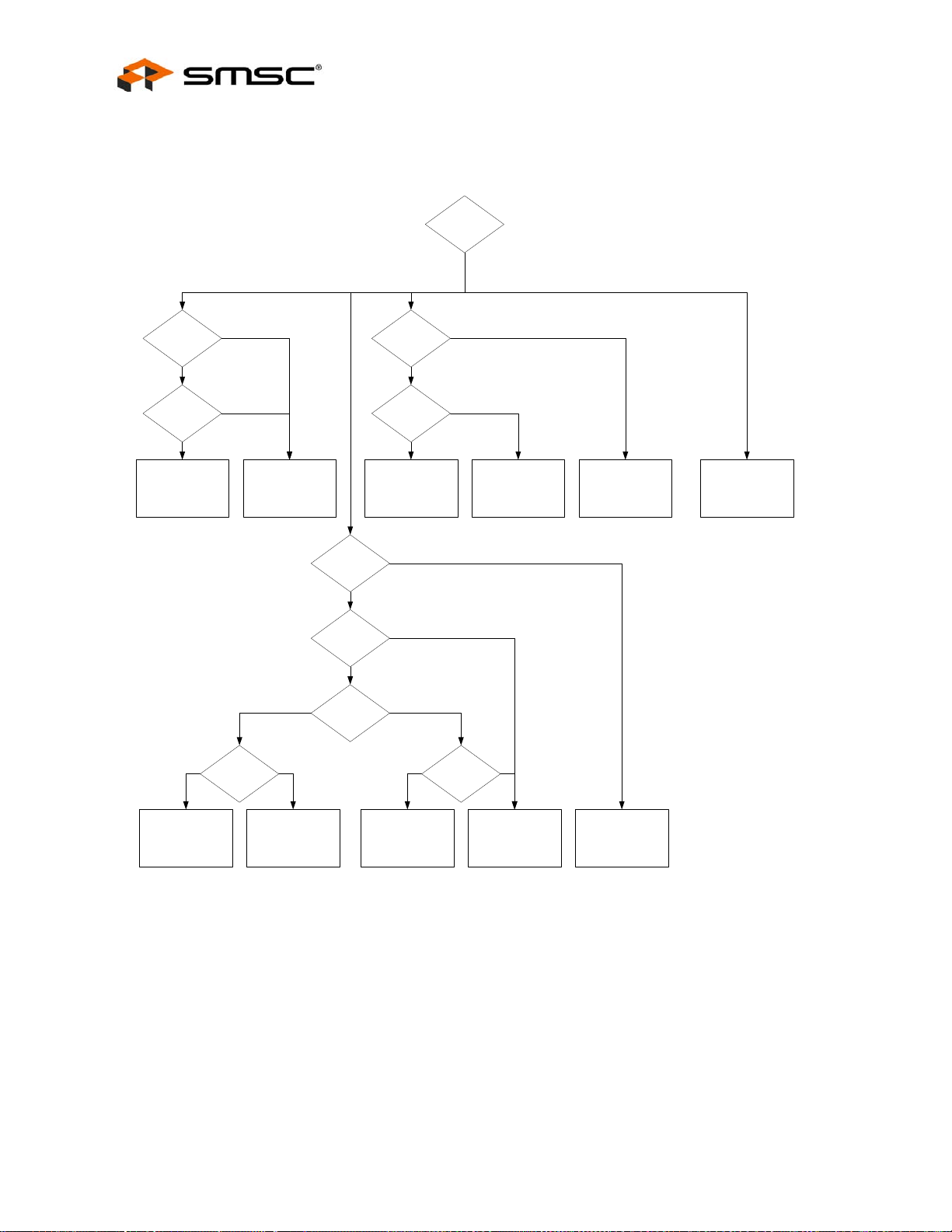
Two Port 10/100 Managed Ethernet Switch with 16-Bit Non-PCI CPU Interface
Datasheet
Hybrid tagging is summarized in Figure 6.9.
Receive Tag
Type
Non-tagged
Insert Tag
[egress_port]
Y
Default VID
[ingress_port]
Un-tag Bit
N
Add Tag
VID = Default VID
[ingress_port]
Priority = Default Priority
[ingress_port]
N
Y
Send Packet Untouched
Normal Tagged
VID = Default VID
Priority = Default Priority
Received VID
Un-tag Bit
N
Change Tag
[egress_port]
Y
Change VLAN ID
Y N
[egress_port]
Priority Tagged
Default VID
[ingress_port]
Un-tag Bit
N
Change Priority
[egress_port]
Y
Modify Tag
[ingress_port ]
[ingress_port ]
Y
N
Y
N
Priority = Uncha nged
Modify Tag
VID = Default VID
[ingress_port]
Strip Tag
Special Tagged
Strip Tag
Change Priority
Y
[egress_port]
Modify Tag
VID = Default VID
[egress_port]
Priority = Default Priority
[egress_port]
N Y
Modify Tag
VID = Default VID
[egress_port]
Priority = Uncha nged
VID = Unchanged
Priority = Default Priority
[egress_port]
Modify Tag
Change Priority
[egress_port]
Send Packet Untouc hed
N
Strip Tag
Figure 6.9 Hybrid Po rt Tagging a nd Un-tagging
The default VLAN ID and priority of each port may be configured via the following registers:
Buffer Manager Port 0 Default VLAN ID and Priority Register (BM_VLAN_MII)
Buffer Manager Port 1 Default VLAN ID and Priority Register (BM_VLAN_1)
Buffer Manager Port 2 Default VLAN ID and Priority Register (BM_VLAN_2)
Revision 1.4 (08-19-08) 80 SMSC LAN9311/LAN9311i
DATASHEET
Page 81

Two Port 10/100 Managed Ethernet Switch with 16-Bit Non-PCI CPU Interface
Datasheet
6.5.7 Counters
A counter is maintained per port that contains the number of packets dropped due to buffer space limits
and ingress rate limit discarding (Red and random Yellow dropping). These counters are accessible
via the following registers:
Buffer Manager Port 0 Drop Count Register (BM_DRP_CNT_SRC_MII)
Buffer Manager Port 1 Drop Count Register (BM_DRP_CNT_SRC_1)
Buffer Manager Port 2 Drop Count Register (BM_DRP_CNT_SRC_2)
A counter is maintained per port that contains the number of packets dropped due solely to ingress
rate limit discarding (Red and random Yellow dropping). This count value can be subtracted from the
drop counter, as described above, to obtain the drop counts due solely to buffer space limits. The
ingress rate drop counters are accessible via the following registers:
Buffer Manager Port 0 Ingress Rate Drop Count Register (BM_RATE_DRP_CNT_SRC_MII)
Buffer Manager Port 1 Ingress Rate Drop Count Register (BM_RATE_DRP_CNT_SRC_1)
Buffer Manager Port 2 Ingress Rate Drop Count Register (BM_RATE_DRP_CNT_SRC_2)
6.6 Switch Fabric Interrupts
The switch fabric is capable of generating multiple maskable interrupts from the buffer manager, switch
engine, and MACs. These interrupts are detailed in Section 5.2.2, "Switch Fabric Interrupts," on
page 51.
SMSC LAN9311/LAN9311i 81 Revision 1.4 (08-19-08)
DATASHEET
Page 82

Chapter 7 Ethernet PHYs
7.1 Functional Overview
The LAN9311/LAN9311i contains three PHYs: Port 1 PHY, Port 2 PHY and a Virtual PHY. The Port 1
& 2 PHYs are identical in functionality and each connect thei r corresponding Ethernet signal pins to
the switch fabric MAC of their respective port. These PHYs interface with their respective MAC via an
internal MII interface. The Virtual PHY provides the virtual functionality of a PH Y and al lows connecti on
of the Host MAC to port 0 of the switch fabric as if it was connected to a single port PHY. All PHYs
comply with the IEEE 802.3 Physical Layer for Twisted Pair Ethernet and can be configured for full/half
duplex 100 Mbps (100BASE-TX) or 10Mbps (10BASE-T) Ethernet operation. All PHY registers follow
the IEEE 802.3 (clause 22.2.4) specified MII management register se t and can be configu red indirectly
via the Host MAC, or directly via the memory mapped Virtual PHY registers. Refer to Section 14.4,
"Ethernet PHY Control and Status Registers" for details on the Ethernet PHY registers.
The LAN9311/LAN9311i Ethernet PHYs are discussed in detail in the following sections:
Section 7.2, "Port 1 & 2 PHYs," on page 83
Section 7.3, "Virtual PHY," on page 96
7.1.1 PHY Addressing
Two Port 10/100 Managed Ethernet Switch with 16-Bit Non-PCI CPU Interface
Datasheet
Each individual PHY is assigned a unique default PHY address via the phy_addr_sel_strap
configuration strap as shown in Table 7.1. In addition, the Port 1 PHY a nd Port 2 PHY addresses can
be changed via the PHY Address (PHYADD) field in the Port x PHY Special Modes Register
(PHY_SPECIAL_MODES_x). For proper operation, all LAN9311/LAN9311i PHY addresses must be
unique. No check is performed to assure each PHY is set to a different address. Configuration strap
values are latched upon the de-assertion of a chip-level reset as described in Section 4.2.4,
"Configuration Straps," on page 40.
PHY_ADDR_SEL_STRAP
0012
1123
Table 7.1 Default PHY Serial MII Addressing
VIRTUAL PHY DEFAULT
ADDRESS VALUE
PORT 1 PHY DEFAULT
ADDRESS VALUE
PORT 2 PHY DEFAULT
ADDRESS VALUE
Revision 1.4 (08-19-08) 82 SMSC LAN9311/LAN9311i
DATASHEET
Page 83
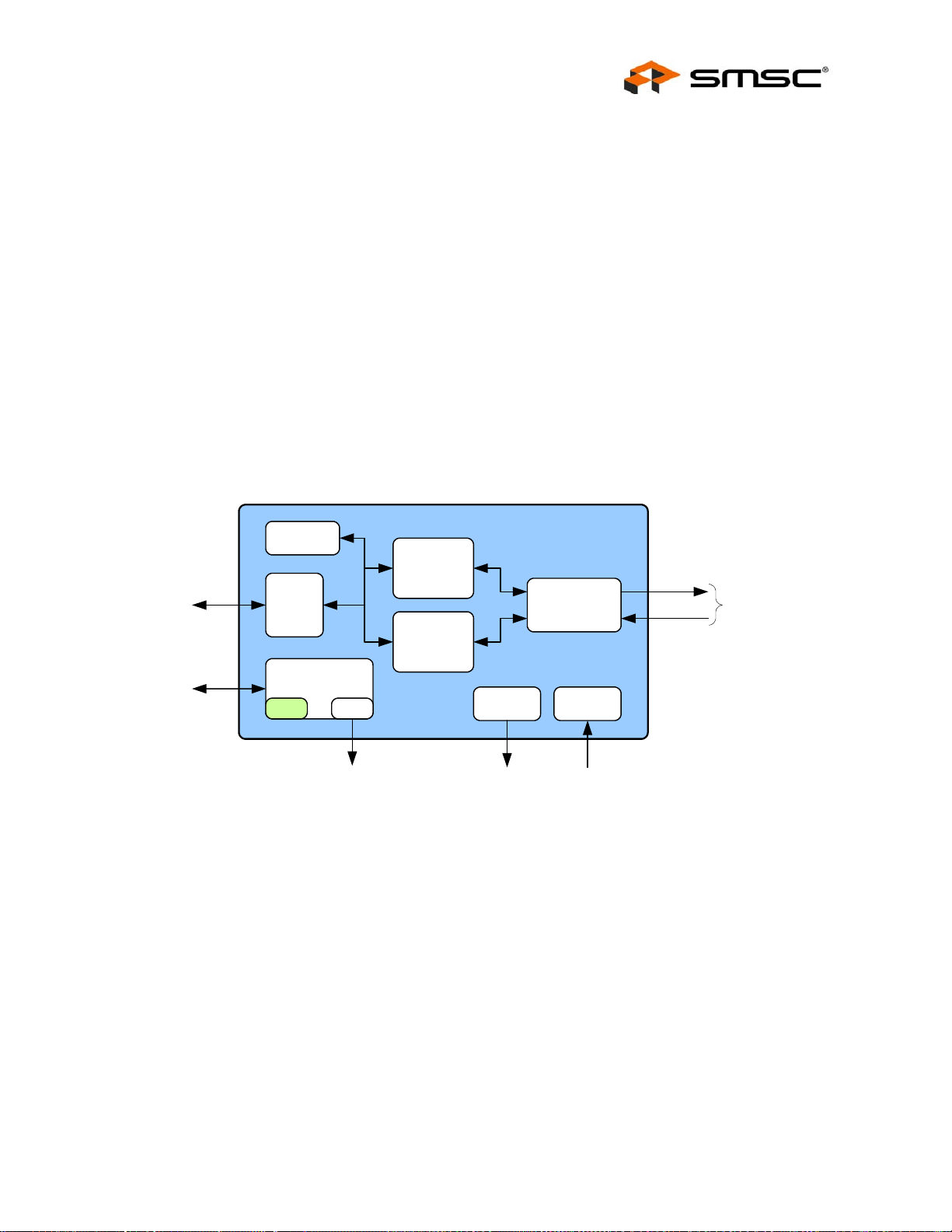
Two Port 10/100 Managed Ethernet Switch with 16-Bit Non-PCI CPU Interface
Datasheet
7.2 Port 1 & 2 PHYs
Functionally, each PHY can be divided into the following sections:
100BASE-TX Transmit and 100BASE-TX Receive
10BASE-T Transmit and 10BASE-T Receive
PHY Auto-negotiation
HP Auto-MDIX
MII MAC Interface
PHY Management Control
Note 7.1 Because the Port 1 PHY and Port 2 PHY are functionally identical, this section will describe
them as the “Port x PHY”, or simply “PHY”. Wherever a lowercase “x” has been append ed
to a port or signal name, it can be repl aced with “1” or “2” to indicate the Port 1 or Port 2
PHY respectively. All references to “PHY” in this section can be used interchangeably for
both the Port 1 & 2 PHYs. This nomenclature excludes the Virtual PHY.
A block diagram of the Port x PHYs main components can be seen in Figure 7.1.
To Port x
Switch Fabric MAC
To Host MAC
MII
MDIO
Auto-
Negotiation
MII
MAC
Interface
PHY Management
Control
Registers
Interrupts
To System
Interrupt Controller
10/100
Transmitter
HP Auto-MDIX
10/100
Reciever
LEDs PLL
To GPIO/LED
Controller
From
System Clocks Controller
Figure 7.1 Port x PHY Bl ock Diagram
TXPx/TXNx
RXPx/RXNx
To External
Port x Ethernet Pins
SMSC LAN9311/LAN9311i 83 Revision 1.4 (08-19-08)
DATASHEET
Page 84
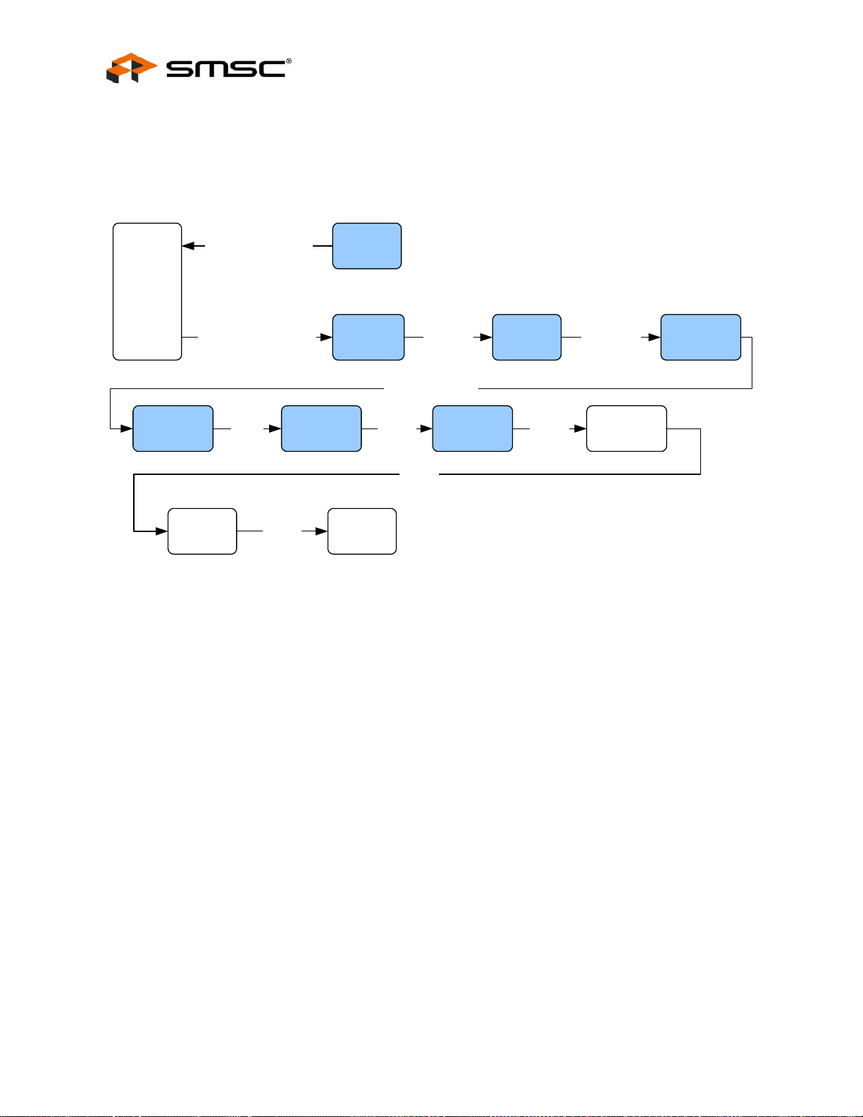
7.2.1 100BASE-TX Transmit
The 100BASE-TX transmit data path is shown in Figure 7.2. Shaded blocks are those which are
internal to the PHY. Each major block is explained in the followi ng sections.
Two Port 10/100 Managed Ethernet Switch with 16-Bit Non-PCI CPU Interface
Datasheet
Internal
MII Transmit Clock
Port x
MAC
Internal
MII 25 MHz by 4 bits
NRZI
Converter
7.2.1.1 MII MAC Interface
For a transmission, the switch fabric MAC drives the transmit data to the PHYs MII MAC Interface.
The MII MAC Interface is described in detail in Section 7.2.7, "MII MAC Interface".
NRZI
Converter
MLT-3
100M
PLL
4B/5B
Encoder
MLT-3
MLT-3
MII MAC
Interface
125 Mbps Serial
MLT-3
25MHz
by 4 bits
100M
TX Driver
MLT-3
CAT-5RJ45
Figure 7.2 100BASE-TX Transmit Data Path
25MHz by
5 bits
Magnetics
Scrambler
and PISO
Note: The PHY is connected to the switch fabric MAC via standard MII signals. Refer to the IEEE
802.3 specification for additional details.
7.2.1.2 4B/5B Encoder
The transmit data passes from the MII block to the 4B/5B Encoder. This block encodes the data from
4-bit nibbles to 5-bit symbols (known as “code-groups”) according to Table 7.2. Each 4-bit data-nibble
is mapped to 16 of the 32 possible code-groups. The remaining 16 code-groups are either used for
control information or are not valid.
The first 16 code-groups are referred to by the hexadecimal values of their corre sponding data nibbles,
0 through F. The remaining code-groups are given le tter designations with slashes on either side. F or
example, an IDLE code-group is /I/, a transmit error code-group is /H/, etc.
Revision 1.4 (08-19-08) 84 SMSC LAN9311/LAN9311i
DATASHEET
Page 85

Two Port 10/100 Managed Ethernet Switch with 16-Bit Non-PCI CPU Interface
Datasheet
Table 7.2 4B/5B Code Table
CODE
GROUP SYM
11110 0 0 0000 DATA 0 0000 DATA
01001 1 1 0001 1 0001
10100 2 2 0010 2 0010
10101 3 3 0011 3 0011
01010 4 4 0100 4 0100
01011 5 5 0101 5 0101
01110 6 6 0110 6 0110
01111 7 7 0111 7 0111
10010 8 8 1000 8 1000
10011 9 9 1001 9 1001
10110 A A 1010 A 1010
10111 B B 1011 B 1011
11010 C C 1100 C 1100
11011 D D 1101 D 1101
RECEIVER
INTERPRETATION
TRANSMITTER
INTERPRETATION
11100 E E 1110 E 1110
11101 F F 1111 F 1111
11111 /I/ IDLE Sent after /T/R/ until the MII Transmitter
11000 /J/ First nibble of SSD, translated to “0101”
following IDLE, else MII Receive Error
(RXER)
10001 /K/ Second nibble of SSD, translated to
“0101” following J, else MII Receive
Error (RXER)
01101 /T/ First nibble of ESD, causes de-assertion
of CRS if followed by /R/, else assertion
of MII Receive Error (RXER)
00111 /R/ Second nibbl e of ESD, causes de-
assertion of CRS if following /T/, else
assertion of MII Receive Error (RXER)
00100 /H/ Transmit Error Symbol Sent for rising MII Transmit Error (TXER)
00110 /V/ INVALID, MII Receive Error (RXER) if
during MII Receive Data Valid (RXDV)
11001 /V/ INVALID, MII Receive Error (RXER) if
during MII Receive Data Valid (RXDV)
00000 /V/ INVALID, MII Receive Error (RXER) if
during MII Receive Data Valid (RXDV)
Enable signal (TXEN) is received
Sent for rising MII Transmitter Enable
signal (TXEN)
Sent for rising MII Transmitter Enable
signal (TXEN)
Sent for falling MII Transmitter Enable
signal (TXEN)
Sent for falling MII Transmitter Enable
signal (TXEN)
INVALID
INVALID
INVALID
00001 /V/ INVALID, MII Receive Error (RXER) if
during MII Receive Data Valid (RXDV)
SMSC LAN9311/LAN9311i 85 Revision 1.4 (08-19-08)
INVALID
DATASHEET
Page 86

Table 7.2 4B/5B Code Table (continued)
Two Port 10/100 Managed Ethernet Switch with 16-Bit Non-PCI CPU Interface
Datasheet
CODE
GROUP SYM
00010 /V/ INVALID, MII Receive Error (RXER) if
during MII Receive Data Valid (RXDV)
00011 /V/ INVALID, MII Receive Error (RXER) if
during MII Receive Data Valid (RXDV)
00101 /V/ INVALID, MII Receive Error (RXER) if
during MII Receive Data Valid (RXDV)
01000 /V/ INVALID, MII Receive Error (RXER) if
during MII Receive Data Valid (RXDV)
01100 /V/ INVALID, MII Receive Error (RXER) if
during MII Receive Data Valid (RXDV)
10000 /V/ INVALID, MII Receive Error (RXER) if
during MII Receive Data Valid (RXDV)
RECEIVER
INTERPRETATION
7.2.1.3 Scrambler and PISO
Repeated data patterns (especially the IDLE code-group) can have power spectral densities wi th large
narrow-band peaks. Scrambling the data helps eliminate these peaks and spread the signal power
more uniformly over the entire channel bandwidth. This uniform spectral density is requ ired by FCC
regulations to prevent excessive EMI from being radiated by the physical wiring. The scrambler also
performs the Parallel In Serial Out conversion (PISO) of the data.
The seed for the scrambler is generated from the PHY address, ensuring that each PHY will have its
own scrambler sequence. For more information on PHY addressing, refer to Section 7.1.1, "PHY
Addressing".
TRANSMITTER
INTERPRETATION
INVALID
INVALID
INVALID
INVALID
INVALID
INVALID
7.2.1.4 NRZI and MLT-3 Encoding
The scrambler block passes the 5-bit wide parallel data to the NRZI converter where it becomes a
serial 125MHz NRZI data stream. The NRZI is then encoded to MLT-3. MLT-3 is a tri-level code where
a change in the logic level represents a code bit “1” and the logic output remaining at the same level
represents a code bit “0”.
7.2.1.5 100M Transmit Driver
The MLT-3 data is then passed to the analog transmit ter, which drives the differential MLT-3 signal on
output pins TXPx and TXNx (where “x” is replaced with “1” for the Port 1 PHY, or “2” for the Port 2
PHY), to the twisted pair media across a 1:1 ratio isolation transformer. The 10BASE-T and 100BASETX signals pass through the same transformer so t hat common “magnet ics” can be used for both. The
transmitter drives into the 100
matching require external components.
Ω impedance of the CAT-5 cable. Cable termination and impedance
7.2.1.6 100M Phase Lock Loop (PLL)
The 100M PLL locks onto the reference clock and generates the 125MHz clock used to drive the 125
MHz logic and the 100BASE-TX Transmitter.
Revision 1.4 (08-19-08) 86 SMSC LAN9311/LAN9311i
DATASHEET
Page 87
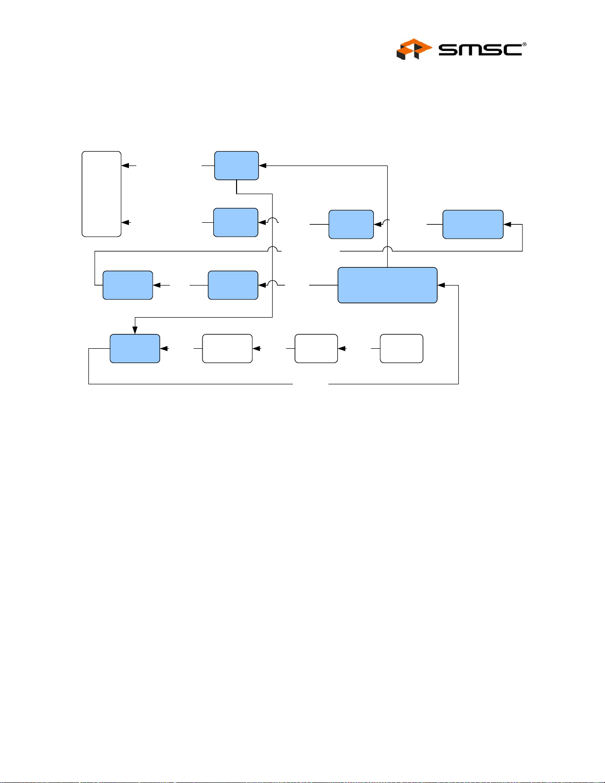
Two Port 10/100 Managed Ethernet Switch with 16-Bit Non-PCI CPU Interface
Datasheet
7.2.2 100BASE-TX Receive
The 100BASE-TX receive data path is shown in Figure 7.3. Shaded blocks are those whic h are internal
to the PHY. Each major block is explained in the foll owing sections.
Internal
MII Receive Clock
Port x
MAC
Internal
MII 25MHz by 4 bits
NRZI
Converter
NRZI
A/D
Converter
7.2.2.1 A/D Converter
100M
PLL
MII MAC
Interface
MLT-3
Converter
Magnetics CAT-5RJ45
Figure 7.3 100BASE-TX Receive Data Path
25MHz
by 4 bits
125 Mbps Serial
MLT-3
6 bit Data
4B/5B
Decoder
DSP: Timing
recovery, Equalizer
and BLW Correction
MLT-3MLT-3 MLT-3
25MHz by
5 bits
Descrambler
and SIPO
The MLT-3 data from the cable is fed into the PHY on inputs RXPx and RXNx (where “x” is replaced
with “1” for the Port 1 PHY, or “2” for the Port 2 PHY) via a 1:1 ratio transformer. The ADC samples
the incoming differential signal at a rate of 125M samples per second. Using a 64-level quantizer, 6
digital bits are generated to represent each sample. The DSP adjusts the gain of the A/D Converter
(ADC) according to the observed signal levels such that the full dynamic range of the ADC can be
used.
7.2.2.2 DSP: Equalizer, BLW Correction and Clock/Data Recovery
The 6 bits from the ADC are fed into the DSP block. The equalizer in th e DSP section compensates
for phase and amplitude distortion caused by the physical channel (magnetics, connectors, and CAT5 cable). The equalizer can restore the signal fo r any good -q ual ity CAT-5 cable between 1m and 150m.
If the DC content of the signal is such that the low-frequency comp onents fall below the low frequency
pole of the isolation transformer, then the droop characteristics of the transformer will become
significant and Baseline Wander (BLW) on the received signal will result. To prevent corruption of the
received data, the PHY corrects for BLW and can receive the ANSI X3.263-1995 FDDI TP-PMD
defined “killer packet” with no bit errors.
The 100M PLL generates multiple phases of the 125MHz clock. A multiplexer, controlled by the timing
unit of the DSP, selects the optimum phase for sampling the data. This is used as the received
recovered clock. This clock is used to extract the serial data from the received signal.
SMSC LAN9311/LAN9311i 87 Revision 1.4 (08-19-08)
DATASHEET
Page 88

7.2.2.3 NRZI and MLT-3 Decoding
The DSP generates the MLT-3 recovered levels th at are fed to the MLT-3 converter. The MLT-3 is then
converted to an NRZI data stream.
7.2.2.4 Descrambler and SIPO
The descrambler performs an inverse function to the scramb ler in the transmitter and also performs
the Serial In Parallel Out (SIPO) conversion of the data.
During reception of IDLE (/I/) symbols. the descrambler synchronizes its descrambler key to the
incoming stream. Once synchronization is achieved, the descrambler locks on this key and is able to
descramble incoming data.
Special logic in the descrambler ensures synchronization with the remote PHY by searching for IDLE
symbols within a window of 4000 bytes (40us). Th is window ensures that a maximum packet size of
1514 bytes, allowed by the IEEE 802.3 standard, can be received with no interference. If no IDLEsymbols are detected within this time-period, receive operation is aborted and the descrambler re-starts
the synchronization process.
The de-scrambled signal is then aligned into 5-bit code-groups by recognizing the /J/K/ Start-of-Stream
Delimiter (SSD) pair at the start of a packet. Once the code-word alignment is determined, it is stored
and utilized until the next start of frame.
Two Port 10/100 Managed Ethernet Switch with 16-Bit Non-PCI CPU Interface
Datasheet
7.2.2.5 5B/4B Decoding
The 5-bit code-groups are translated into 4-bit data nibbles according to the 4B/5B table shown in
Table 7.2. The translated data is presented on the internal MII RXD[3:0] signal lin es to the switch fabric
MAC. The SSD, /J/K/, is translated to “0101 0101” as the first 2 nibbles of the MAC preamble.
Reception of the SSD causes the PHY to assert the RXDV signal, indicating that valid data is available
on the RXD bus. Successive valid code-groups are translated to data nibbles. Reception of either the
End of Stream Delimiter (ESD) consisting of the /T/R/ symbols, or at least two /I/ symbols causes the
PHY to de-assert carrier sense and RXDV. These symbols are not translated into data.
7.2.2.6 Receiver Errors
During a frame, unexpected code-groups are considered receive errors. Expect ed code groups are the
DATA set (0 through F), and the /T/R/ (ESD) symbol pair. When a receive error occurs, the internal
MII’s RXER signal is asserted and arbitrary data is driven onto the internal receive data bus (RXD) to
the switch fabric MAC. Should an error be detected during the time that the /J/K/ delimiter is being
decoded (bad SSD error), RXER is asserted and the value 1110b is driven onto the internal receive
data bus (RXD) to the switch fabric MAC. Note that the internal MII’s data valid signal (RXDV) is not
yet asserted when the bad SSD occurs.
7.2.2.7 MII MAC Interface
For reception, the 4-bit data nibbles are sent to the MII MAC Interface bl ock where they are sent via
MII to the switch fabric MAC. The MII MAC Interface is described in detail in Section 7.2.7, "MII MAC
Interface".
Note: The PHY is connected to the switch fabric MAC via standard MII signals. Refer to the IEEE
802.3 specification for additional details.
Revision 1.4 (08-19-08) 88 SMSC LAN9311/LAN9311i
DATASHEET
Page 89

Two Port 10/100 Managed Ethernet Switch with 16-Bit Non-PCI CPU Interface
Datasheet
7.2.3 10BASE-T Transmit
Data to be transmitted comes from the switch fabric MAC. The 10BASE-T transmitter receives 4-bit
nibbles from the internal MII at a rate of 2.5MHz and converts them to a 10Mbps serial data stream.
The data stream is then Manchester-encoded and sent to the analog transmitter, which drives a signal
onto the twisted pair via the external magnetics.
10BASE-T transmissions use the following blocks:
MII MAC Interface (digital)
10M TX Driver (digital/analog)
10M PLL (analog)
7.2.3.1 MII MAC Interface
For a transmission, the switch fabric MAC drives the transmit data to the PHYs MII MAC Interface.
The MII MAC Interface is described in detail in Section 7.2.7, "MII MAC Int erface".
Note: The PHY is connected to the switch fabric MAC via standard MII signals. Refer to the IEEE
802.3 specification for additional details.
7.2.3.2 10M TX Driver and PLL
The 4-bit wide data is sent to the 10M TX Driver block. The nibbl es are converted to a 10Mbps serial
NRZI data stream. The 10M PLL locks onto the external clock or internal oscillator and produces a
20MHz clock. This is used to Manchester encode the NRZ data stream. When no data is being
transmitted (TXEN is low), the 10M TX Driver block outputs Normal Link Pulses (NLPs) to maintain
communications with the remote link partner. The manchester encoded data is sent to the analog
transmitter where it is shaped and filtered before being driven out as a differential signal across t he
TXPx and TXNx outputs (where “x” is replaced with “1” for the Port 1 PHY, or “2” for the Port 2 PHY).
7.2.4 10BASE-T Receive
The 10BASE-T receiver gets the Manchester-encoded analog signal from the cable via the magnetics.
It recovers the receive clock from the signal and uses this clock to recover the NRZI data stream. This
10M serial data is converted to 4-bit data nibbles which are passed to the controller across the intern al
MII at a rate of 2.5MHz.
10BASE-T reception uses the following blocks:
Filter and SQUELCH (analog)
10M RX (digital/analog)
MII MAC Interface (digital)
10M PLL (analog)
7.2.4.1 Filter and Squelch
The Manchester signal from the cable is fed into the PHY on inputs RXPx and RXNx (where “x” is
replaced with “1” for Port 1, or “2” for Port 2) via 1 :1 ratio magnetics. It is first filtered to reduce any
out-of-band noise. It then passes through a SQUELCH circuit. The SQUELCH is a set of amplitude
and timing comparators that normally reject differential voltage levels below 300mV and detect and
recognize differential voltages above 585mV.
7.2.4.2 10M RX and PLL
The output of the SQUELCH goes to the 10M RX block where it is validated as Manchest er encoded
data. The polarity of the signal is also checked. If the polarity is reversed (local RXP is connected to
RXN of the remote partner and vice versa), then this is ident ified a nd co rrec ted. The reversed conditi on
is indicated by the flag “XPOL“, bit 4 in Port x PHY Special Control/Status Indication Register
SMSC LAN9311/LAN9311i 89 Revision 1.4 (08-19-08)
DATASHEET
Page 90

(PHY_SPECIAL_CONTROL_STAT_IND_x). The 10M PLL locks onto the received Manchester signal
and generates the received 20MHz clock from it. Using this clock, the Manchester encode d data is
extracted and converted to a 10MHz NRZI data stream. It is then converted from serial to 4-bit wide
parallel data.
The RX10M block also detects valid 10BASE-T IDLE signals - Normal Link Pulses (NLPs) - to maintain
the link.
7.2.4.3 MII MAC Interface
For reception, the 4-bit data nibbles are sent to the MII MAC Interface bl ock where they are sent via
MII to the switch fabric MAC. The MII MAC Interface is described in detail in Section 7.2.7, "MII MAC
Interface".
Note: The PHY is connected to the switch fabric MAC via standard MII signals. Refer to the IEEE
802.3 specification for additional details.
7.2.4.4 Jabber Detection
Jabber is a condition in which a station transmits for a period of time longer than the maximum
permissible packet length, usually due to a fault condition, t hat results in holding the TXEN input for
an extended period of time. Special logic is used to detect the jabber state and abort the transmission
to the line, within 45ms. Once TXEN is deasserted, the l ogic resets the jabber condition.
Two Port 10/100 Managed Ethernet Switch with 16-Bit Non-PCI CPU Interface
Datasheet
7.2.5 PHY Auto-negotiation
The purpose of the auto-negotiation function is t o automatically configure the PHY to the optimum link
parameters based on the capabilities of its link partner. Auto-negotiation is a mechanism for
exchanging configuration information between two lin k-partners and automatically sel ecting the hi ghest
performance mode of operation supported by both sides. Auto-negotiation is fully define d in clause 28
of the IEEE 802.3 specification and is enabled by setting bit 12 (PHY_AN) of the Port x PHY Basic
Control Register (PHY_BASIC_CONTROL_x).
The advertised capabilities of the PHY are stored in the Port x PHY Auto-Negotiation Advertisement
Register (PHY_AN_ADV_x). The PHY contains the ability to advertise 100BASE-TX and 10BASE-T in
both full or half-duplex modes. Besides the connection speed, the PHY can advertise remote fault
indication and symmetric or asymmetric pause flow control as defined in the IEEE 802.3 specification.
The LAN9311/LAN9311i does not support “Next Page” capability. Many of the default advertised
capabilities of the PHY are determined via configuration straps as shown in Section 14.4.2.5, "Port x
PHY Auto-Negotiation Advertisement Register (PHY_AN_ADV_x)," on page 295. Refer to Section
4.2.4, "Configuration Straps," on page 40 for additional details on how to use the LAN9311/LAN9311i
configuration straps.
Once auto-negotiation has completed, information about the resolved link and the results of the
negotiation process are reflected in the speed indication bits in the Port x PHY Special Control/Status
Register (PHY_SPECIAL_CONTROL_STATUS_x), as well as the Port x PHY Auto-Negotiation Link
Partner Base Page Ability Register (PHY_AN_LP_BASE_ABILITY_x).
The auto-negotiation protocol is a purely physical layer activity and proceeds independently of the MAC
controller.
The following blocks are activated during an Auto-negot iation session:
Auto-negotiation (digital)
100M ADC (analog)
100M PLL (analog)
100M equalizer/BLW/clock recovery (DSP)
10M SQUELCH (analog)
Revision 1.4 (08-19-08) 90 SMSC LAN9311/LAN9311i
DATASHEET
Page 91

Two Port 10/100 Managed Ethernet Switch with 16-Bit Non-PCI CPU Interface
Datasheet
10M PLL (analog)
10M TX Driver (analog)
Auto-negotiation is started by the occurrence of any of the following events:
Power-On Reset (POR)
Hardware reset (nRST)
PHY Software reset (via Reset Control Register (RESET_CTL), or bit 15 of the Port x PHY Basic
Control Register (PHY_BASIC_CONTROL_x))
PHY Power-down reset (Section 7.2.9, "PHY Power-Down Modes," on page 94 )
PHY Link status down (bit 2 of the Port x PHY Basic Status Register (PHY_BASIC_STATUS_x) is
cleared)
Setting the Port x PHY Basic Control Register (PHY_BASIC_CONTROL_x), bit 9 high (auto-neg
restart)
Digital Reset (via bit 0 of the Reset Control Register (RESET_CTL))
Issuing an EEPROM Loader RELOAD command (Section 10.2.4, "EEPROM Loader," on page 150)
Note: Refer to Section 4.2, "Resets," on page 36 for information on these and other system resets.
On detection of one of these events, the PHY begins auto-ne gotiation by transmitting bursts of Fast
Link Pulses (FLP). These are bursts of link pulses from the 10M TX Driver. They are shaped as Normal
Link Pulses and can pass uncorrupted down CAT-3 or CAT-5 cable. A Fast Link Pulse Burst consists
of up to 33 pulses. The 17 odd-numbered pulses, which are always present, frame the F LP burst. The
16 even-numbered pulses, which may be present or absent , contain the data word being transmitted.
Presence of a data pulse represents a “1”, while absence represents a “0”.
The data transmitted by an FLP burst is known as a “Link Code Word.” These are defined fully in IEEE
802.3 clause 28. In summary, the PHY advertises 802.3 compliance in its selector field (the first 5 bits
of the Link Code Word). It advertises its technology abili ty according to the bits set in the Port x PHY
Auto-Negotiation Advertisement Register (PHY_AN_ADV_x).
There are 4 possible matches of the technology abilities. In the order of priority these are:
100M Full Duplex (highest priority)
100M Half Duplex
10M Full Duplex
10M Half Duplex (lowest priority)
If the full capabilities of the PHY are advertised (100M, full-duplex), and if the link partner is capable
of 10M and 100M, then auto-negotiation selects 100M as the high est performance mode. If the link
partner is capable of half and full-duplex modes, then auto-negotiation selects full-duplex as the highest
performance mode.
Once a speed and duplex match has been determined, the link code words are repeated with the
acknowledge bit set. Any difference in the main content of the link code words at this time will cause
auto-negotiation to re-start. Auto-negotiation will also re-start if all of the required FLP bursts are not
received.
Writing the Port x PHY Auto-Negotiation Advertisement Register (PHY_AN_ADV_x) bits [8:5] allows
software control of the capabilities advertised by the PHY. Writing the Port x PHY Auto-Negotiation
Advertisement Register (PHY_AN_ADV_x) does not automatically re-start auto-negotiat ion. The Port
x PHY Basic Control Register (PHY_BASIC_CONTROL_x), bit 9 must be set before the new abi lities
will be advertised. Auto-negotiation can also b e disabled via software by clearing bit 12 of the Port x
PHY Basic Control Register (PHY_BASIC_CONTROL_x).
SMSC LAN9311/LAN9311i 91 Revision 1.4 (08-19-08)
DATASHEET
Page 92

7.2.5.1 PHY Pause Flow Control
The Port 1 & 2 PHYs are capable of generating and receiving pause flow control frames per the IEEE
802.3 specification. The PHYs advertised pause flow control abili ties are set via bits 10 (Symmetric
Pause) and 11 (Asymmetric Pause) of the Port x PHY Auto-Negotiation Advertisement Register
(PHY_AN_ADV_x). This allows the PHY to advertise its flow control abilities and auto-negotiate the
flow control settings with its link partner. The default values of these bits are determined via
configuration straps as defined in Section 14.4.2.5, "Port x PHY Auto-Negotiation Advertisement
Register (PHY_AN_ADV_x)," on page 295.
The pause flow control settings may also be manually set via the manual flow control reg isters Port 1
Manual Flow Control Register (MANUAL_FC_1) and Port 2 Manual Flow Control Register
(MANUAL_FC_2). These registers allow the switch fabric ports flow control settings t o be manually set
when auto-negotiation is disabled or the Manu al Flow Control Se lect bit 0 is set. The currently enabled
duplex and flow control settings can also be monitored via these registers. The flow control values in
the Port x PHY Auto-Negotiation Advertisement Register (PHY_AN_ADV_x) are not affected by the
values of the manual flow control register. Refer to Section 6.2.3, "Flow Control Enable Logic," on
page 58 for additional information.
7.2.5.2 Parallel Detection
If the LAN9311/LAN9311i is connected to a device lacking the a bility to auto-negotiate (i.e. no FLPs
are detected), it is able to determine the speed of the link based on either 100M MLT-3 symbols or
10M Normal Link Pulses. In this case the link is presumed to be half-duplex per the IEEE 802.3
standard. This ability is known as “Parallel Detection.” This feature ensures interoperability with legacy
link partners. If a link is formed via parallel d etection, then bit 0 in the Port x PHY Auto-Negotiation
Expansion Register (PHY_AN_EXP_x) is cleared to indicate that the link partner is not capable of auto-
negotiation. If a fault occurs during parallel detection, bit 4 of the Port x PHY Auto-Negotiation
Expansion Register (PHY_AN_EXP_x) is set.
Two Port 10/100 Managed Ethernet Switch with 16-Bit Non-PCI CPU Interface
Datasheet
The Port x PHY Auto-Negotiation Link Partner Base Page Ability Register
(PHY_AN_LP_BASE_ABILITY_x) is used to store the Link Partner Ability information, which is coded
in the received FLPs. If the link partner is not auto-negotiation capable, then this register is updated
after completion of parallel detection to reflect the speed capability of the link partner.
7.2.5.3 Restarting Auto-Negotiation
Auto-negotiation can be re-started at any time by setting bit 9 of the Port x PHY Basic Cont rol Register
(PHY_BASIC_CONTROL_x). Auto-negotiation will also re-start if the link is broken at any time. A
broken link is caused by signal loss. This may occur because of a cable break, or because of an
interruption in the signal transmitted by the Link Partner. Auto-negotiation resumes in an attemp t to
determine the new link configuration.
If the management entity re-starts Auto-negotiation by writi ng to bit 9 of the Port x PHY Basic Control
Register (PHY_BASIC_CONTROL_x), the LAN9311/LAN9311i will respond by stopping all
transmission/receiving operations. Once the internal break link time of approximately 1200ms has
passed in the Auto-negotiation state-machine, the auto-ne gotiation will re-start. In this case, the link
partner will have also dropped the link due to lack of a received signal, so it too will resume autonegotiation.
7.2.5.4 Disabling Auto-Negotiation
Auto-negotiation can be disabled by clearing bit 12 of the Port x PHY Basic Control Register
(PHY_BASIC_CONTROL_x). The PHY will then force its speed of operation to reflect the speed (bit
13) and duplex (bit 8) of the Port x PHY Basic Control Register (PHY_BASIC_CONTROL_x). The
speed and duplex bits in the Port x PHY Basic Control Register (PHY_BASIC_CONTROL_x) should
be ignored when auto-negotiation is enabled.
Revision 1.4 (08-19-08) 92 SMSC LAN9311/LAN9311i
DATASHEET
Page 93

Two Port 10/100 Managed Ethernet Switch with 16-Bit Non-PCI CPU Interface
Datasheet
7.2.5.5 Half Vs. Full-Duplex
Half-duplex operation relies on the CSMA/CD (Carrier Sense Multiple Access / Collision Detect)
protocol to handle network traffic and collisions. In this mode, the carrier sense signa l, CRS, responds
to both transmit and receive activity. If data is received while the PHY is transmitting, a collision results.
In full-duplex mode, the PHY is able to transmit and receive data simultaneously. In this mode, CRS
responds only to receive activity. The CSMA/CD protocol does not apply and collision detection is
disabled.
7.2.6 HP Auto-MDIX
HP Auto-MDIX facilitates the use of CAT-3 (10 BASE-T) or CAT-5 (100 BASE-T) media UTP
interconnect cable without consideration of interface wiring scheme. If a user plugs in either a direct
connect LAN cable or a cross-over patch cable, as shown in Figure 7.4 (See Note 7.1 on page 83), t he
PHY is capable of configuring the TXPx/TXNx and RXPx/RXNx twisted pair pins for correct transceiver
operation.
The internal logic of the device detects the TX and RX pins of the connecting device. Since the RX
and TX line pairs are interchangeable, special PCB design considerations are needed to accommo dat e
the symmetrical magnetics and termination of an Auto-MDIX design.
The Auto-MDIX function can be disabled through bit 15 (AMDIXCTRL) of the Port x PHY Special
Control/Status Indication Register (PHY_SPECIAL_CONTROL_STAT_IND_x). When AMDIXCTRL is
cleared, Auto-MDIX can be selected via the auto_ md ix_str ap_x co nf igura tion st rap. T he MDIX can a lso
be configured manually via the manual_mdix_strap_x if both the AMDIXCTRL bit and the
auto_mdix_strap_x configuration strap are low. Refer to Section 3.2, "Pin Descriptions," on page 28 for
more information on the configuration straps.
When bit 15 (AMDIXCTRL) of the Port x PHY Special Control/Status Indication Register
(PHY_SPECIAL_CONTROL_STAT_IND_x) is set to 1, the Auto-MDIX capability is determined by bits
13 and 14 of the Port x PHY Special Control/Status Indication Register
(PHY_SPECIAL_CONTROL_STAT_IND_x).
RJ-45 8-pin straight-through
for 10BASE-T/100BASE-TX
signaling
TXPx
1
TXNx
2
RXPx
3
Not Used
Not Used
Not Used
Not Used
RXNx
4
5
6
7
8
Direct Connect Cable
Figure 7.4 Direct Cable Connection vs. Cross-Over Cable Connection
7.2.7 MII MAC Interface
1
2
3
4
5
6
7
8
TXPx
TXNx
RXPx
Not Used
Not Used
RXNx
Not Used
Not Used
TXPx
TXNx
RXPx
Not Used
Not Used
RXNx
Not Used
Not Used
RJ-45 8-pin cross-over fo r
10BASE-T/100BASE-TX
signaling
1
2
3
4
5
6
7
8
Cross-Over Cable
1
2
3
4
5
6
7
8
TXPx
TXNx
RXPx
Not Used
Not Used
RXNx
Not Used
Not Used
The MII MAC Interface is responsible for the transmission and rece ption of the Ethernet data to and
from the switch fabric MAC. The PHY is connected internally to the switch fabric MAC via standard
MII signals per IEEE 802.3.
SMSC LAN9311/LAN9311i 93 Revision 1.4 (08-19-08)
DATASHEET
Page 94

For a transmission, the switch fabric MAC drives the transmit data onto the internal MII TXD bus and
asserts TXEN to indicate valid data. The data is in the form of 4-bit wide data at a rate of 25MHz for
100BASE-TX, or 2.5MHz for 10BASE-T.
For reception, the 4-bit data nibbles are sent to the MII MAC Interface block. Th ese data nibbles are
clocked to the controller at a rate of 25MHz for 100BASE-TX, or 2.5MHz for 10BASE-T. RXCLK is the
output clock for the internal MII bus. It is recovered from th e received data to clock the RXD bus. If
there is no received signal, it is derived from the system reference clock.
7.2.8 PHY Management Control
The PHY Management Control block is responsible for the management functions of the PHY,
including register access and interrupt generation. A Serial Management Interface (SMI) is used to
support registers 0 through 6 as required by the IEEE 802.3 (Clause 22), as well as the vend or specific
registers allowed by the specification. The SMI interfac e consists of the MII Management Data (MDIO)
signal and the MII Management Clock (MDC) signal. These signals interface to the Host MAC and
allow access to all PHY registers. Refer to Section 14.4.2, "Port 1 & 2 PHY Registers," on page 287
for a list of all supported registers and register descriptions. Non-supported registers will be read as
FFFFh.
7.2.8.1 PHY Interrupts
The PHY contains the ability to generate various interrupt events as described in Table 7.3. Reading
the Port x PHY Interrupt Source Flags Register (PHY_INTERRUPT_SOURCE_x) shows the source of
the interrupt, and clears the interrupt signal. The Port x PHY Interrupt Mask Register
(PHY_INTERRUPT_MASK_x) enables or disables each PHY interrupt. The PHY Management Control
block aggregates the enabled interrupts status into an internal signal which is sent to the System
Interrupt Controller and is reflected via the Inte rrupt Status Register (INT_STS) bit 26 (PHY_INT1) for
the Port 1 PHY, and bit 27 (PHY_INT2) for the Port 2 PHY. For more information on the
LAN9311/LAN9311i interrupts, refer to Chapter 5, "System Int errupts," on page 49.
Two Port 10/100 Managed Ethernet Switch with 16-Bit Non-PCI CPU Interface
Datasheet
Table 7.3 PHY Interrupt Sources
INTERRUPT SOURCE
ENERGYON Activated 7
Auto-Negotiation Complete 6
Remote Fault Detected 5
Link Down (Link Status Negated) 4
Auto-Negotiation LP Acknowledge 3
Parallel Detection Fault 2
Auto-Negotiation Page Received 1
7.2.9 PHY Power-Down Modes
There are two power-down modes for the PHY:
PHY General Power-Down
PHY Energy Detect Power-Down
Note: Fo r more information on the various power management features of the LAN9311/LAN9311i,
refer to Section 4.3, "Power Management," on page 4 6.
PHY_INTERRUPT_SOURCE_x REGISTER BIT #
PHY_INTERRUPT_MASK_x &
Revision 1.4 (08-19-08) 94 SMSC LAN9311/LAN9311i
DATASHEET
Page 95

Two Port 10/100 Managed Ethernet Switch with 16-Bit Non-PCI CPU Interface
Datasheet
Note: The power-down modes of each PHY (Port 1 PHY and Port 2 PHY) are controlled
independently.
Note: The PHY p ower-down modes do not reload or reset the PHY registers.
7.2.9.1 PHY General Power-Down
This power-down mode is controlled by bit 11 of the Port x PHY Basic Control Register
(PHY_BASIC_CONTROL_x). In this mode the entire PHY, except the PHY management control
interface, is powered down. The PHY will remain in this power-down state as long as bit 11 is set.
When bit 11 is cleared, the PHY powers up and is automatically reset.
7.2.9.2 PHY Energy Detect Power-Down
This power-down mode is enabled by setting bit 13 (EDPWRDOWN) of the Port x PHY Mode
Control/Status Register (PHY_MODE_CONTROL_STATUS_x). When in this mode, if no energy is
detected on the line, the entire PHY is powered down except for the PHY management control
interface, the SQUELCH circuit, and the ENERGYON logic. The ENERGYON logic is used to detect
the presence of valid energy from 100BASE-TX, 10BASE-T, or auto-negotiation signals and is
responsible for driving the ENERGYON signal (bit 1) of the Port x PH Y Mode Control/Status Register
(PHY_MODE_CONTROL_STATUS_x).
In this mode, when the ENERGYON signal is cleared, the PHY is powered down and no data is
transmitted from the PHY. When energy is received, via link pulses or packets, the ENERGYON signal
goes high, and the PHY powers up. The PHY automatically resets itself into its previous state prior to
power-down, and asserts the INT7 interrupt (bit 7) of the Port x PHY Interrupt Source Flags Register
(PHY_INTERRUPT_SOURCE_x). The first and possibly second packet to activate ENERGYON may
be lost.
When bit 13 (EDPWRDOWN) of the Port x PHY Mode Control/Status Register
(PHY_MODE_CONTROL_STATUS_x) is low, energy detect power-down is disabled.
The energy detect power down feature is part of the broader power management features of the
LAN9311/LAN9311i and can be used to trigger the power management event output p in (PME). This
is accomplished by enabling the energy detect power-down feature of the PHY as described above,
and setting the corresponding energy detect enable (b it 14 for Port 1 PHY, bit 15 for Port 2 PHY) of
the Power Mana gement Control Register (PMT_CTRL). Refer to Section 4.3, "Power Management,"
on page 46 for additional information.
7.2.10 PHY Resets
In addition to the chip-level hardware reset (nRST) and Power-On Reset (POR), the PHY supports
three block specific resets. These are discussed in the following section s. For detailed information on
all LAN9311/LAN9311i resets and the reset sequence refer to Section 4.2, "Resets," on page 36 .
Note: Th e DIGITAL_RST bit in the Reset Control Register (RESET_CTL) does not reset the PHYs.
Only a hardware reset (nRST) or an EEPROM RELOAD command will automatically reload
the configuration strap values into the PHY registers. For all other PHY resets, these values
will need to be manually configured via software.
7.2.10.1 PHY Software Reset via RESET_CTL
The PHY can be reset via the Reset Control Register (RESET_CTL). The Port 1 PHY is reset by
setting bit 1 (PHY1_RST), and the Port 2 PHY is reset by setting bit 2 (PHY2_RST). These bi ts are
self clearing after approximately 102uS. This reset does not reload the configuration stra p values into
the PHY registers.
SMSC LAN9311/LAN9311i 95 Revision 1.4 (08-19-08)
DATASHEET
Page 96

Two Port 10/100 Managed Ethernet Switch with 16-Bit Non-PCI CPU Interface
7.2.10.2 PHY Software Reset via PHY_BASIC_CTRL_x
The PHY can also be reset by setting bit 15 (PHY_RST) of the Port x PHY Basic Control Register
(PHY_BASIC_CONTROL_x). This bit is self clearing and will return to 0 after the reset is complete.
This reset does not reload the configuration strap values in to the PHY registers.
7.2.10.3 PHY Power-Down Reset
After the PHY has returned from a power-down state, a reset of the PHY is automatically generat ed.
The PHY power-down modes do not reload or reset the PHY registers. Refer to Section 7.2.9, "PHY
Power-Down Modes," on page94 for additional informa tion.
7.2.11 LEDs
Each PHY provides LED indication signals to the GPIO/LED block of the LAN9311/LAN9311i. This
allows external LEDs to be used to indicate various PHY related functions such as TX/RX activity,
speed, duplex, or link status. Refer to C hapter 13, "GPIO/LED Controller," on page 163 for additional
information on the configuration of these signal s.
7.2.12 Required Ethernet Magnetics
The magnetics selected for use with the LAN9311/LAN9311i should be an Auto-MDIX style magnetic,
which is widely available from several vendors. Please review the SMSC Application note 8.13
“Suggested Magnetics” for the latest qualified and suggested magnetics. A list of vendors and part
numbers are provided within the application note.
Datasheet
7.3 Virtual PHY
The Virtual PHY provides a basic MII management interface (MDIO) to the Host MAC per the IEEE
802.3 (clause 22) so that an unmodified dri ver can be supported as if the Host MAC wa s attached to
a single port PHY. This functionality is designed to allow easy and quick integration of the
LAN9311/LAN9311i into designs with minimal driver modifi cations. The Virtual PHY provides a full bank
of registers which comply with the IEEE 802.3 specification. This enables the Virtual PHY to provide
various status and control bits similar to those provided by a real PHY. These include the output of
speed selection, duplex, loopback, isolate, collision test, and auto-negotiation status. For a list of all
Virtual PHY registers and related bit descriptions, refer to Section 14.4.1, "Virtual PHY Registers," on
page 287.
7.3.1 Virtual PHY Auto-Negotiation
The purpose of the auto-negotiation function is to automatically configure the Virtual PHY to the
optimum link parameters based on the capabilities of its link partner. Because the Virtual PHY has no
actual link partner, the auto-negotiation process is emulated with deterministic results.
Auto-negotiation is enabled by setting bit 12 (VPHY_AN) of the Virtual PHY Basic Control Register
(VPHY_BASIC_CTRL) and is restarted by the occurrence of any of the following events:
Power-On Reset (POR)
Hardware reset (nRST)
PHY Software reset (via bit 3 of the Reset Control Register (RESET_CTL), bit 0 of the Power
Management Control Register (PMT_CTRL), or bi t 15 of the Virtual PHY Basic Control Register
(VPHY_BASIC_CTRL))
Setting the Virtual PHY Basic Control Register (VPHY_BASIC_CTRL), bit 9 high (auto-neg restart)
Digital Reset (via bit 10 of the Reset Control Register (RESET_CTL))
Issuing an EEPROM Loader RELOAD command (Section 10.2.4, "EEPROM Loader," on page 150)
Revision 1.4 (08-19-08) 96 SMSC LAN9311/LAN9311i
DATASHEET
Page 97

Two Port 10/100 Managed Ethernet Switch with 16-Bit Non-PCI CPU Interface
Datasheet
The emulated auto-negotiation process is much simpler than the real process and can be categorized
into three steps:
1. Bit 5 (Auto-Negotiation Complete) is set in the Virtual PHY Basic Status Register
(VPHY_BASIC_STATUS).
2. Bit 1 (Page Received) is set in the Virtual PHY Auto-Negotiation Expansion Register
(VPHY_AN_EXP).
3. The auto-negotiation result (speed and duplex) is determined and regi stered.
The auto-negotiation result (speed and dup lex) is dete rmined usin g the Highe st Common Deno minator
(HCD) of the Virtual PHY Auto-Negotiation Advertisement Register (VPHY_AN_ADV) and Vir tua l P HY
Auto-Negotiation Link Partner Base Page Ability Register (VPHY_AN_LP_BASE_ABILITY) as
specified in the IEEE 802.3 standard. The technology ability bits of these registers are ANDed, and if
there are multiple bits in common, the priority is determined as follows:
100Mbps Full Duplex (highest priority)
100Mbps Half Duplex
10Mbps Full Duplex
10Mbps Half Duplex (lowest priority)
For example, if the full capabilities of the Virtual PHY are advertised (10 0Mbps, Full Duplex), and if
the link partner is capable of 10Mbps and 100Mbps, then auto-negotiation selects 100Mbps as the
highest performance mode. If the link partner is capable of half and full-duplex modes, then autonegotiation selects full-duplex as the highest performance operation. In the event that there are no bi ts
in common, an emulated Parallel Detection is used.
The Virtual PHY Auto-Negotiation Advertisement Register (VPHY_AN_ADV) defaults to having all four
ability bits set. These values can be reconfigured via software. Once the auto-negotiation is complete,
any change to the Virtual PHY Auto-Negotiation Advertisement Register (VPHY_AN_ADV) will not take
affect until the auto-negotiation process is re-run. The emulated link partner always advertises all four
abilities (100BASE-X full duplex, 100BASE-X half duplex, 10BASE-T full duplex, and 10BASE-T half
duplex) in the Virtual PHY Auto-Negotiation Link Partner Base Page Ability Register
(VPHY_AN_LP_BASE_ABILITY). Neither the Virtual PHY or the emulated link partner support next
page capability, remote faults, or 100BASE-T4.
If there is at least one common selection between the emulated link partner and the Virtual PHY
advertised abilities, then the auto-negotiation su cceeds, the Link Partner Auto-Negotiation Able bit 0
of the Virtual PHY Auto-Negotiation Expansion Register (VPHY_AN_EXP) is set, and the technology
ability bits in the Virtual PHY Auto-Negotiation Link Partner Base Page Ability Register
(VPHY_AN_LP_BASE_ABILITY) are set to indicate the emulated link partners abilities.
Note: For t he Virtual PHY, the auto-negotiation register bits (and management of such) are used by
the Host MAC. So the perception of local and link partner is reversed. The local device is the
Host MAC, while the link partner is the switch fabric. This is consistent with the intention of the
Virtu al PH Y.
7.3.1.1 Parallel Detection
In the event that there are no common bits between the advertised ability and the emulated link
partners ability, auto-negotiation fails and emulated parallel detect is used. In this case, the Link
Partner Auto-Negotiation Able (bit 0) in the Virtual PHY Auto-Negotiation Expansion Register
(VPHY_AN_EXP) will be cleared, and the communication set to 100Mbps half-duplex. Only one of the
technology ability bits in the Virtual PHY Auto-Negotiation Link Partner Base Page Ability Register
(VPHY_AN_LP_BASE_ABILITY) will be set, indicating the emulated parallel detect result.
7.3.1.2 Disabling Auto-Negotiation
Auto-negotiation can be disabled in the Virtual PHY by clearing bit 12 (VPHY_AN) of the Virtual PHY
Basic Control Register (VPHY_BASIC_CTRL). The Virtual PHY will then force its speed of operation
to reflect the speed (bit 13) and duplex (bit 8) of the Virtual PHY Basic Control Register
SMSC LAN9311/LAN9311i 97 Revision 1.4 (08-19-08)
DATASHEET
Page 98

(VPHY_BASIC_CTRL). The speed and duplex bits in the Virtual PHY Basic Control Register
(VPHY_BASIC_CTRL) should be ignored when auto-negotiation is enabled.
7.3.1.3 Virtual PHY Pause Flow Control
The Virtual PHY supports pause flow control per the IEEE 802.3 specification. The Virtual PHYs
advertised pause flow control abilities are set via bits 10 (Symmetric Pause) and 11 (Asymmetric
Pause) of the Virtual PHY Auto-Negotiation Advertisement Register (VPHY_AN_ADV). This allows the
Virtual PHY to advertise its flow control abilities and auto-ne gotiate the flow control settings with the
emulated link partner. The default values of these bits are as shown in Section 14.2.8.5, "Virtual PHY
Auto-Negotiation Advertisement Register (VPHY_AN_ADV)," on page 253 .
The symmetric/asymmetric pause ability of the emulated link partner is based upon the advertised
pause flow control abilities of the Virtual PHY in (bits 10 & 11) of the Virtual PHY Auto-Negotiation
Advertisement Register (VPHY_AN_ADV). Thus, the emulated link partner always accommodates t he
asymmetric/symmetric pause ability settings requested by the Virtual PHY, as shown in Table 14.5,
“Emulated Link Partner Pause Flow Control Ability Default Values,” on page 256.
The pause flow control settings may also be manually set via the Port 0(Host MAC) Manual Flow
Control Register (MANUAL_FC_MII). This register allows the switch fabric port 0 flow cont rol settings
to be manually set when auto-negotiat ion is disabled or the Manual Flow Control Select b it 0 is set.
The currently enabled duplex and flow control settings can also be monitore d via this regist er. The flow
control values in the Virtual PHY Auto-Negotiation Advertisement Register (VPHY_AN_ADV) are not
affected by the values of the manual flow control register. Refer to Section 6.2.3, "Flow Control Enable
Logic," on page 58 for additional info rmation.
Two Port 10/100 Managed Ethernet Switch with 16-Bit Non-PCI CPU Interface
Datasheet
7.3.2 Virtual PHY Resets
In addition to the chip-level hardware reset (nRST) and Power-On Reset (POR), the Virtual PHY
supports three block specific resets. These are is discussed in the following sections. For detailed
information on all LAN9311/LAN9311i resets, refer to Section 4.2, "Resets," on page 36.
7.3.2.1 Virtual PHY Software Reset via RESET_CTL
The Virtual PHY can be reset via the Reset Control Register (RESET_CTL) by setting bit 3
(VPHY_RST). This bit is self clearing after approximately 102uS.
7.3.2.2 Virtual PHY Software Reset via VPHY_BASIC_CTRL
The Virtual PHY can also be reset by setting bit 15 (VPHY_RST) of the Virtual PHY Basic Control
Register (VPHY_BASIC_CTRL). This bit is self clearing and will return to 0 after the reset is complete.
7.3.2.3 Virtual PHY Software Reset via PMT_CTRL
The Virtual PHY can be reset via the Power Management Co ntrol Register (PMT_CTRL) by sett ing bit
10 (VPHY_RST). This bit is self clearing after approximatel y 102uS.
Revision 1.4 (08-19-08) 98 SMSC LAN9311/LAN9311i
DATASHEET
Page 99

Two Port 10/100 Managed Ethernet Switch with 16-Bit Non-PCI CPU Interface
Datasheet
Chapter 8 Host Bus Interface (HBI)
8.1 Functional Overview
The Host Bus Interface (HBI) module provides a high -speed asynchronous SRAM-like slave interface
that facilitates communication between the LAN9311/LAN9311i and a host system. The HBI allows
access to the System CSRs and handles byte swapping based on the dynamic endianess select. The
HBI interfaces to the switch fabric via the Host MAC, which contains the TX/RX Data and Status FIFOs,
Host MAC registers and power management features. Refer to Chapter 9, "Host MAC," on page 113
for detailed information on the Host MAC.
The following is an overview of the functions provided by t he HBI:
Asynchronous 16-bit Host Bus Interface: T he HBI provides an asynchronous SRAM-like Host Bus
Interface that is compatible with most CPUs.
Host data bus endianess control: The HBI supports dynamic selection of big and little endian
host byte ordering based on the END_SEL input pin. This highly flexible interface provides mixed
endian access for registers and memory.
Direct FIFO access modes: When the FIFO_SEL input pin is hi gh during host access, all host
write operations are to the TX data FIFO and all host read operati ons are from the RX data FIFOs.
This feature facilitates operation with host DMA controllers that do not support FIFO operations.
System CSR’s: The HBI allows for configuration and monitoring of the various LAN9311/LAN9311i
functions through the System Control and Status Registers (CSRs). These registers are accessible to
the host via the Host Bus Interface and a llow direct (and in direct) access to a ll the LAN9311/LAN9311i
functions. For a full list of all System CSR’s and their descriptions, refer to Section 14.2, "System
Control and Status Registers".
Interrupt support: The HBI supports a variety of interrupt sources. Individual interrupts can be
monitored and enabled/disabled via registers within t he System CSRs for output on the IRQ pin. For
more information on interrupts, refer to Chapter 5, "System Interrupts," on page 49.
For a list of all HBI related pins, refer to Table 3.4 on page 30 in Chapter 3, Pin Description and
Configuration.
8.2 Host Memory Mapping
The host memory map has two unique modes: norma l operation mode, and direct FIFO access mode.
During normal operation, the base address decode map is as described in Figure14.1 on page 167,
allowing access to the full range of System Management CSRs and the TX/RX Data and Status FIFOs.
This is the default mode of operation. The second mode of operation is the direct FIF O access mode.
In direct FIFO access mode, all host write operations are to the TX Data FIFO and all host read
operations are from the RX Data FIFO. Refer to Section 14.1.3, "Direct FIFO Access Mode," on
page 168 for additional inf ormation.
8.3 Host Data Bus
The host data bus is 16-bits wide. Two writes or reads must be performed back-to-back, as detailed
below, for proper communication.
Note: When accessing the device, the pair of cycles must be atomic. The first host bus cycle is
performed to the low/high WORD and the second host bus cycle is perfo rmed to the high/low
WORD forming a 32-bit transaction with no cycles to the LAN9311/LAN9311i in between. With
the exception of A[1], all address and control signals must be the same for both 16-bit cycles
of a 32-bit transaction.
SMSC LAN9311/LAN9311i 99 Revision 1.4 (08-19-08)
DATASHEET
Page 100

8.3.1 16-Bit Bus Writes
The host is required to perform two contiguous 16-bit writes to complete a single DWORD transfer.
The DWORD must not cross a DWORD address boundary (A[2] and higher cannot change betwe en
a pair of writes). No ordering requirements exist. The host can access either the low or high word first,
as long as the next write is performed on the other word. If a write to the same word is performe d, the
device disregards the transfer. Once both writes occur, an internal 32-bit write is performed to the
appropriate register.
8.3.2 16-Bit Bus Read
The host is required to perform two consecutive 16-bit reads to complete a single DWORD transf er.
The DWORD must not cross a DWORD address boundary (A[2] and higher cannot change betwe en
a pair of writes). No ordering requirements exist. The host can access either the low or high word first,
as long as the next read is performed from the other word. If a read to the same word is performed,
the data read is invalid and should be re-read. However, this is not a fatal error. The
LAN9311/LAN9311i will reset its read counters and restart a new cycle on the next read.
Note: Some regist ers are readable as 16-bit registers. In this case, if desired, only one 16-bit read
may be performed without the need to read the other word. If a re gister is 16-bit readable, it
will be noted in its register description.
Two Port 10/100 Managed Ethernet Switch with 16-Bit Non-PCI CPU Interface
Datasheet
8.4 Host Endianess
The LAN9311/LAN9311i supports big and little endian host byte ordering based upon t he END_SEL
pin. When END_SEL is low, host access is little endian. When END_SEL is high, host access is big
endian. In a typical application, END_SEL is connected to a high-order address line, making endian
selection address based. This highly flexible interface provides mixe d endian access for registers and
memory for both PIO and host DMA access. As an example, PIO transfers to/from the System CSRs
can utilize a different byte ordering than host DM A transactions to/from the RX and TX Data FIFOs.
All internal busses are 32-bit with little en dian byte ordering. Logic within the host bus interface reorders bytes based on the state of the endian select signal (END_SEL), and the state of the least
significant address line (A1).
Data path operations for the supported endian configurations are illustrated in Figure 8.1, "Little Endian
Byte Ordering" and Figure 8.2, "Big Endian Byte Ordering".
Revision 1.4 (08-19-08) 100 SMSC LAN9311/LAN9311i
DATASHEET
 Loading...