

Page 1

LAN91C111
10/100 Non-PCI
Ethernet Single Chip
MAC + PHY
PRODUCT FEATURES
Singl e Chip Ethernet Controller
Du al Speed - 10/100 Mbps
F ully Supports Full Duplex Switched Ethernet
Sup ports Burst Data Transfer
8 Kbytes Internal Memory for Receive and Transmit
FIFO Buffers
Enh anced Power Management Features
Optional Configuration via Serial EEPROM Interface
Sup ports 8, 16 and 32 Bit CPU Accesses
Interna l 32 Bit Wide Data Path (Into Packet Buffer
Memory)
Bui lt-in Transparent Arbitration for Slave Sequential
Access Architecture
Flat MMU Architecture with Symmetric Transmit and
Receive Structures and Queues
3 .3V Operation with 5V Tolerant IO Buffers (See Pin
List Description for Additional Details)
Sin gle 25 MHz Reference Clock for Both PHY and
MAC
External 25Mhz-output pin for an external PHY
supporting PHYs physical media.
L ow Power CMOS Design
Sup ports Multiple Embedded Processor Host
Interfaces
—ARM
—SH
— Power PC
— Coldfire
— 680X0, 683XX
— MIPS R3000
Datasheet
3 .3V MII (Media Independent Interface) MAC-PHY
Interface Running at Nibble Rate
MII Management Serial Interface
128-Pin QFP package; lead-free RoHS compliant
package also available.
1 28-Pin TQFP package, 1.0 mm height; lead-free
RoHS compliant package also available.
C ommercial Temperature Range from 0 °C to 70°C
(LAN91C111)
Ind ustrial Temperature Range from -40°C to 85°C
(LAN91C111i)
Network Interface
Fully Integrated IEEE 802.3/802.3u-100Base-TX/
10Base-T Physical Layer
Au to Negotiation: 10/100, Full / Half Duplex
On C hip Wave Shaping - No External Filters
Required
Ad aptive Equalizer
Ba seline Wander Correction
L ED Outputs (User selectable – Up to 2 LED
functions at one time)
—Link
—Activity
— Full Duplex
— 10/100
— Transmit
— Receive
SMSC LAN91C111 REV C DATASHEET Revision 1.91 (08-18-08)
Page 2

10/100 Non-PCI Ethernet Single Chip MAC + PHY
ORDER NUMBERS:
LAN91C111-NC, LAN91C111i-NC (INDUSTRIAL TEMPERATURE)
FOR 128-PIN QFP PACKAGES
LA N 91 C 111- N S, L AN 9 1C 111 i- N S (INDUSTRIAL TEMPERATURE)
FOR 128-PIN QFP LEAD-FREE ROHS COMPLIANT PACKAGES
LAN91C111-NE (1.0MM HEIGHT); LAN91C111i-NE (INDUSTRIAL TEMPERATURE)
FOR 128-PIN TQFP PACKAGES
LAN91C111-NU (1.0MM HEIGHT); LAN91C111i-NU (INDUSTRIAL TEMPERATURE)
FOR 128-PIN TQFP LEAD-FREE ROHS COMPLIANT PACKAGES
Datasheet
80 ARKAY DRIVE, HAUPPAUGE, NY 11788 (631) 435-6000, FAX (631) 273-3123
Copyright © 2008 SMSC or its subsidiaries. All rights reserved.
Circuit diagrams and other information relating to SMSC products are included as a mean s of illustrating typical applications. Conse quently, complete information sufficient for
construction purposes is not necessarily given. Although the information has been checked and is believed to be accurate, no responsibility is assumed for inaccuracies. SMSC
reserves the right to make changes to specifications and product descriptions at any time without notice. Contact your local SMSC sales office to obtain the latest specifications
before placing your product order. The provision of this information does not convey to the purchaser of the described semiconductor devices any licenses under any patent
rights or other intellectual property rights of SMSC or others. All sales are expressly conditional on your agreement to the terms and conditions of the most recently dated
version of SMSC's standard Terms of Sale Agreement dated before the date of your order (the "Terms of Sale Agreement"). The product may contain design defects or errors
known as anomalies which may cause the product's functions to deviate from published specifications. Anomaly sheets are available upon request. SMSC products are not
designed, intended, authorized or warranted for use in any life support or other application where product failure could cause or contribute to personal injury or severe property
damage. Any and all such uses without prior written approval of an Officer of SMSC and further testing and/or modification will be fully at the risk of the customer. Copies of
this document or other SMSC literature, as well as the Terms of Sale Agreement, may be obtained by visiting SMSC’s website at http://www.smsc.com. SMSC is a registered
trademark of Standard Microsystems Corporation (“SMSC”). Product names and company names are the trademarks of their respective holders.
SMSC DISCLAIMS AND EXCLUDES ANY AND ALL WARRANTIES, INCLUDING WITHOUT LIMITATION ANY AND ALL IMPLIED WARRANTIES OF MERCHANTABILITY,
FITNESS FOR A PARTICULAR PURPOSE, TITLE, AND AGAINST INFRINGEMENT AND THE LIKE, AND ANY AND ALL WARRANTIES ARISING FROM ANY COURSE
OF DEALING OR USAGE OF TRADE. IN NO EVENT SHALL SMSC BE LIABLE FOR ANY DIRECT, INCIDENTAL, INDIRECT, SPECIAL, PUNITIVE, OR CONSEQUENTIAL
DAMAGES; OR FOR LOST DATA, PROFITS, SAVINGS OR REVENUES OF ANY KIND; REGARDLESS OF THE FORM OF ACTION, WHETHER BASED ON CONTRACT;
TORT; NEGLIGENCE OF SMSC OR OTHE RS; STRICT LIABILITY; BREACH OF WARRANTY; OR OTHERWISE; WHETHER OR NOT ANY REMEDY OF BUYER IS HELD
TO HAVE FAILED OF ITS ESSENTIAL PURPOSE, AND WHETHER OR NOT SMSC HAS BEEN ADVISED OF THE POSSIBILITY OF SUCH DAMAGES.
Revision 1.91 (08-18-08) 2 SMSC LAN91C111 REV C
DATASHEET
Page 3

10/100 Non-PCI Ethernet Single Chip MAC + PHY
Datasheet
Table of Contents
Chapter 1 General Description. . . . . . . . . . . . . . . . . . . . . . . . . . . . . . . . . . . . . . . . . . . . . . . . . 8
Chapter 2 Pin Configurations. . . . . . . . . . . . . . . . . . . . . . . . . . . . . . . . . . . . . . . . . . . . . . . . . . 9
Chapter 3 Block Diagrams . . . . . . . . . . . . . . . . . . . . . . . . . . . . . . . . . . . . . . . . . . . . . . . . . . . 11
Chapter 4 Signal Descriptions . . . . . . . . . . . . . . . . . . . . . . . . . . . . . . . . . . . . . . . . . . . . . . . . 14
Chapter 5 Description of Pin Functions. . . . . . . . . . . . . . . . . . . . . . . . . . . . . . . . . . . . . . . . . 15
Chapter 6 Signal Description Parameters. . . . . . . . . . . . . . . . . . . . . . . . . . . . . . . . . . . . . . . 19
6.1 Buffer Types . . . . . . . . . . . . . . . . . . . . . . . . . . . . . . . . . . . . . . . . . . . . . . . . . . . . . . . . . . . . . . . . . . 19
Chapter 7 Functional Description . . . . . . . . . . . . . . . . . . . . . . . . . . . . . . . . . . . . . . . . . . . . . 20
7.1 Clock Generator Block . . . . . . . . . . . . . . . . . . . . . . . . . . . . . . . . . . . . . . . . . . . . . . . . . . . . . . . . . . 20
7.2 CSMA/CD Block . . . . . . . . . . . . . . . . . . . . . . . . . . . . . . . . . . . . . . . . . . . . . . . . . . . . . . . . . . . . . . . 20
7.2.1 DMA Block. . . . . . . . . . . . . . . . . . . . . . . . . . . . . . . . . . . . . . . . . . . . . . . . . . . . . . . . . . . . 20
7.2.2 Arbiter Block . . . . . . . . . . . . . . . . . . . . . . . . . . . . . . . . . . . . . . . . . . . . . . . . . . . . . . . . . . 20
7.3 MMU Block . . . . . . . . . . . . . . . . . . . . . . . . . . . . . . . . . . . . . . . . . . . . . . . . . . . . . . . . . . . . . . . . . . . 20
7.4 BIU Block . . . . . . . . . . . . . . . . . . . . . . . . . . . . . . . . . . . . . . . . . . . . . . . . . . . . . . . . . . . . . . . . . . . . 21
7.5 MAC-PHY Interface . . . . . . . . . . . . . . . . . . . . . . . . . . . . . . . . . . . . . . . . . . . . . . . . . . . . . . . . . . . . 21
7.5.1 Management Data Software Implementation . . . . . . . . . . . . . . . . . . . . . . . . . . . . . . . . . 21
7.5.2 Management Data Timing . . . . . . . . . . . . . . . . . . . . . . . . . . . . . . . . . . . . . . . . . . . . . . . . 22
7.5.3 MI Serial Port Frame Structure . . . . . . . . . . . . . . . . . . . . . . . . . . . . . . . . . . . . . . . . . . . . 22
7.5.4 MII Packet Data Communication with External PHY. . . . . . . . . . . . . . . . . . . . . . . . . . . . 24
7.6 Serial EEPROM Interface . . . . . . . . . . . . . . . . . . . . . . . . . . . . . . . . . . . . . . . . . . . . . . . . . . . . . . . 25
7.7 Internal Physical Layer . . . . . . . . . . . . . . . . . . . . . . . . . . . . . . . . . . . . . . . . . . . . . . . . . . . . . . . . . 25
7.7.1 MII Disable. . . . . . . . . . . . . . . . . . . . . . . . . . . . . . . . . . . . . . . . . . . . . . . . . . . . . . . . . . . . 27
7.7.2 Encoder . . . . . . . . . . . . . . . . . . . . . . . . . . . . . . . . . . . . . . . . . . . . . . . . . . . . . . . . . . . . . . 27
7.7.3 Decoder. . . . . . . . . . . . . . . . . . . . . . . . . . . . . . . . . . . . . . . . . . . . . . . . . . . . . . . . . . . . . . 27
7.7.4 Clock and Data Recovery . . . . . . . . . . . . . . . . . . . . . . . . . . . . . . . . . . . . . . . . . . . . . . . . 29
7.7.5 Scrambler . . . . . . . . . . . . . . . . . . . . . . . . . . . . . . . . . . . . . . . . . . . . . . . . . . . . . . . . . . . . 29
7.7.6 Descrambler . . . . . . . . . . . . . . . . . . . . . . . . . . . . . . . . . . . . . . . . . . . . . . . . . . . . . . . . . . 29
7.7.7 Twisted Pair Transmitter . . . . . . . . . . . . . . . . . . . . . . . . . . . . . . . . . . . . . . . . . . . . . . . . . 30
7.7.8 Twisted Pair Receiver . . . . . . . . . . . . . . . . . . . . . . . . . . . . . . . . . . . . . . . . . . . . . . . . . . . 33
7.7.9 Collision. . . . . . . . . . . . . . . . . . . . . . . . . . . . . . . . . . . . . . . . . . . . . . . . . . . . . . . . . . . . . . 35
7.7.10 Start of Packet. . . . . . . . . . . . . . . . . . . . . . . . . . . . . . . . . . . . . . . . . . . . . . . . . . . . . . . . . 35
7.7.11 End of Packet . . . . . . . . . . . . . . . . . . . . . . . . . . . . . . . . . . . . . . . . . . . . . . . . . . . . . . . . . 36
7.7.12 Link Integrity & AutoNegotiation . . . . . . . . . . . . . . . . . . . . . . . . . . . . . . . . . . . . . . . . . . . 37
7.7.13 Jabber . . . . . . . . . . . . . . . . . . . . . . . . . . . . . . . . . . . . . . . . . . . . . . . . . . . . . . . . . . . . . . . 40
7.7.14 Receive Polarity Correction. . . . . . . . . . . . . . . . . . . . . . . . . . . . . . . . . . . . . . . . . . . . . . . 40
7.7.15 Full Duplex Mode. . . . . . . . . . . . . . . . . . . . . . . . . . . . . . . . . . . . . . . . . . . . . . . . . . . . . . . 41
7.7.16 Loopback. . . . . . . . . . . . . . . . . . . . . . . . . . . . . . . . . . . . . . . . . . . . . . . . . . . . . . . . . . . . . 41
7.7.17 PHY Powerdown . . . . . . . . . . . . . . . . . . . . . . . . . . . . . . . . . . . . . . . . . . . . . . . . . . . . . . . 41
7.7.18 PHY Interrupt. . . . . . . . . . . . . . . . . . . . . . . . . . . . . . . . . . . . . . . . . . . . . . . . . . . . . . . . . . 41
7.8 Reset . . . . . . . . . . . . . . . . . . . . . . . . . . . . . . . . . . . . . . . . . . . . . . . . . . . . . . . . . . . . . . . . . . . . . . . 42
Chapter 8 MAC Data Structures and Registers . . . . . . . . . . . . . . . . . . . . . . . . . . . . . . . . . . 43
8.1 Frame Format In Buffer Memory . . . . . . . . . . . . . . . . . . . . . . . . . . . . . . . . . . . . . . . . . . . . . . . . . . 43
8.2 Receive Frame Status . . . . . . . . . . . . . . . . . . . . . . . . . . . . . . . . . . . . . . . . . . . . . . . . . . . . . . . . . . 44
8.3 I/O Space . . . . . . . . . . . . . . . . . . . . . . . . . . . . . . . . . . . . . . . . . . . . . . . . . . . . . . . . . . . . . . . . . . . . 45
SMSC LAN91C111 REV C 3 Revision 1.91 (08-18-08)
DATASHEET
Page 4

10/100 Non-PCI Ethernet Single Chip MAC + PHY
Datasheet
8.4 Bank Select Register . . . . . . . . . . . . . . . . . . . . . . . . . . . . . . . . . . . . . . . . . . . . . . . . . . . . . . . . . . . 46
8.5 Bank 0 - Transmit Control Register . . . . . . . . . . . . . . . . . . . . . . . . . . . . . . . . . . . . . . . . . . . . . . . . 47
8.6 Bank 0 - EPH Status Register . . . . . . . . . . . . . . . . . . . . . . . . . . . . . . . . . . . . . . . . . . . . . . . . . . . . 48
8.7 Bank 0 - Receive Control Register . . . . . . . . . . . . . . . . . . . . . . . . . . . . . . . . . . . . . . . . . . . . . . . . . 49
8.8 Bank 0 - Counter Register . . . . . . . . . . . . . . . . . . . . . . . . . . . . . . . . . . . . . . . . . . . . . . . . . . . . . . . 50
8.9 Bank 0 - Memory Information Register. . . . . . . . . . . . . . . . . . . . . . . . . . . . . . . . . . . . . . . . . . . . . . 51
8.10 Bank 0 - Receive/Phy Control Register . . . . . . . . . . . . . . . . . . . . . . . . . . . . . . . . . . . . . . . . . . . . . 51
8.11 Bank 1 - Configuration Register . . . . . . . . . . . . . . . . . . . . . . . . . . . . . . . . . . . . . . . . . . . . . . . . . . . 54
8.12 Bank 1 - Base Address Register. . . . . . . . . . . . . . . . . . . . . . . . . . . . . . . . . . . . . . . . . . . . . . . . . . . 55
8.13 Bank 1 - Individual Address Registers . . . . . . . . . . . . . . . . . . . . . . . . . . . . . . . . . . . . . . . . . . . . . . 55
8.14 Bank 1 - General Purpose Register . . . . . . . . . . . . . . . . . . . . . . . . . . . . . . . . . . . . . . . . . . . . . . . . 56
8.15 Bank 1 - Control Register . . . . . . . . . . . . . . . . . . . . . . . . . . . . . . . . . . . . . . . . . . . . . . . . . . . . . . . . 57
8.16 Bank 2 - MMU Command Register. . . . . . . . . . . . . . . . . . . . . . . . . . . . . . . . . . . . . . . . . . . . . . . . . 58
8.17 Bank 2 - Packet Number Register . . . . . . . . . . . . . . . . . . . . . . . . . . . . . . . . . . . . . . . . . . . . . . . . . 59
8.18 Bank 2 - FIFO Ports Register . . . . . . . . . . . . . . . . . . . . . . . . . . . . . . . . . . . . . . . . . . . . . . . . . . . . . 60
8.19 Bank 2 - Pointer Register . . . . . . . . . . . . . . . . . . . . . . . . . . . . . . . . . . . . . . . . . . . . . . . . . . . . . . . . 61
8.20 Bank 2 - Data Register . . . . . . . . . . . . . . . . . . . . . . . . . . . . . . . . . . . . . . . . . . . . . . . . . . . . . . . . . . 62
8.21 Bank 2 - Interrupt Status Registers. . . . . . . . . . . . . . . . . . . . . . . . . . . . . . . . . . . . . . . . . . . . . . . . . 62
8.22 Bank 3 - Multicast Table Registers. . . . . . . . . . . . . . . . . . . . . . . . . . . . . . . . . . . . . . . . . . . . . . . . . 66
8.23 Bank 3 - Management Interface. . . . . . . . . . . . . . . . . . . . . . . . . . . . . . . . . . . . . . . . . . . . . . . . . . . 67
8.24 Bank 3 - Revision Register . . . . . . . . . . . . . . . . . . . . . . . . . . . . . . . . . . . . . . . . . . . . . . . . . . . . . . . 67
8.25 Bank 3 - RCV Register . . . . . . . . . . . . . . . . . . . . . . . . . . . . . . . . . . . . . . . . . . . . . . . . . . . . . . . . . . 68
8.26 Bank 7 - External Registers . . . . . . . . . . . . . . . . . . . . . . . . . . . . . . . . . . . . . . . . . . . . . . . . . . . . . . 68
Chapter 9 PHY MII Registers . . . . . . . . . . . . . . . . . . . . . . . . . . . . . . . . . . . . . . . . . . . . . . . . 70
9.1 Register 0. Control Register . . . . . . . . . . . . . . . . . . . . . . . . . . . . . . . . . . . . . . . . . . . . . . . . . . . . . . 74
9.2 Register 1. Status Register. . . . . . . . . . . . . . . . . . . . . . . . . . . . . . . . . . . . . . . . . . . . . . . . . . . . . . . 75
9.3 Register 2&3. PHY Identifier Register . . . . . . . . . . . . . . . . . . . . . . . . . . . . . . . . . . . . . . . . . . . . . . 76
9.4 Register 4. Auto-Negotiation Advertisement Register . . . . . . . . . . . . . . . . . . . . . . . . . . . . . . . . . . 76
9.5 Register 5. Auto-Negotiation Remote End Capability Register . . . . . . . . . . . . . . . . . . . . . . . . . . . 77
9.6 Register 16. Configuration 1- Structure and Bit Definition . . . . . . . . . . . . . . . . . . . . . . . . . . . . . . . 78
9.7 Register 17. Configuration 2 - Structure and Bit Definition. . . . . . . . . . . . . . . . . . . . . . . . . . . . . . . 79
9.8 Register 18. Status Output - Structure and Bit Definition . . . . . . . . . . . . . . . . . . . . . . . . . . . . . . . . 80
9.9 Register 19. Mask - Structure and Bit Definition . . . . . . . . . . . . . . . . . . . . . . . . . . . . . . . . . . . . . . 81
9.10 Register 20. Reserved - Structure and Bit Definition. . . . . . . . . . . . . . . . . . . . . . . . . . . . . . . . . . . 82
Chapter 10 Software Driver and Hardware Sequence Flow . . . . . . . . . . . . . . . . . . . . . . . . . 84
10.1 Software Driver and Hardware Sequence Flow for Power Management. . . . . . . . . . . . . . . . . . . . 84
10.2 Typical Flow of Events for Transmit (Auto Release = 0). . . . . . . . . . . . . . . . . . . . . . . . . . . . . . . . . 85
10.3 Typical Flow of Events for Transmit (Auto Release = 1). . . . . . . . . . . . . . . . . . . . . . . . . . . . . . . . . 86
10.4 Typical Flow of Event For Receive . . . . . . . . . . . . . . . . . . . . . . . . . . . . . . . . . . . . . . . . . . . . . . . . . 87
Chapter 11 Board Setup Information . . . . . . . . . . . . . . . . . . . . . . . . . . . . . . . . . . . . . . . . . . . 95
Chapter 12 Application Considerations. . . . . . . . . . . . . . . . . . . . . . . . . . . . . . . . . . . . . . . . . . 98
Chapter 13 Operational Description . . . . . . . . . . . . . . . . . . . . . . . . . . . . . . . . . . . . . . . . . . . 105
13.1 Maximum Guaranteed Ratings* . . . . . . . . . . . . . . . . . . . . . . . . . . . . . . . . . . . . . . . . . . . . . . . . . . 105
13.2 DC Electrical Characteristics . . . . . . . . . . . . . . . . . . . . . . . . . . . . . . . . . . . . . . . . . . . . . . . . . . . . 105
13.3 Twisted Pair Characteristics, Transmit. . . . . . . . . . . . . . . . . . . . . . . . . . . . . . . . . . . . . . . . . . . . . 108
13.4 Twisted Pair Characteristics, Receive . . . . . . . . . . . . . . . . . . . . . . . . . . . . . . . . . . . . . . . . . . . . . 109
Chapter 14 Timing Diagrams . . . . . . . . . . . . . . . . . . . . . . . . . . . . . . . . . . . . . . . . . . . . . . . . . 110
Revision 1.91 (08-18-08) 4 SMSC LAN91C111 REV C
DATASHEET
Page 5

10/100 Non-PCI Ethernet Single Chip MAC + PHY
Datasheet
Chapter 15 Package Outlines . . . . . . . . . . . . . . . . . . . . . . . . . . . . . . . . . . . . . . . . . . . . . . . . . 126
Chapter 16 Revision History. . . . . . . . . . . . . . . . . . . . . . . . . . . . . . . . . . . . . . . . . . . . . . . . . . 128
SMSC LAN91C111 REV C 5 Revision 1.91 (08-18-08)
DATASHEET
Page 6

10/100 Non-PCI Ethernet Single Chip MAC + PHY
Datasheet
List of Figures
Figure 2.1 Pin Configuration - LAN91C111-FEAST 128 PIN TQFP . . . . . . . . . . . . . . . . . . . . . . . . . . . . . 9
Figure 2.2 Pin Configuration - LAN91C111-FEAST 128 PIN QFP . . . . . . . . . . . . . . . . . . . . . . . . . . . . . 10
Figure 3.1 Basic Functional Block Diagram . . . . . . . . . . . . . . . . . . . . . . . . . . . . . . . . . . . . . . . . . . . . . . 11
Figure 3.2 Block Diagram . . . . . . . . . . . . . . . . . . . . . . . . . . . . . . . . . . . . . . . . . . . . . . . . . . . . . . . . . . . . 12
Figure 3.3 LAN91C111 Physical Layer to Internal MAC Block Diagram. . . . . . . . . . . . . . . . . . . . . . . . . 13
Figure 7.1 MI Serial Port Frame Timing Diagram . . . . . . . . . . . . . . . . . . . . . . . . . . . . . . . . . . . . . . . . . . 23
Figure 7.2 MII Frame Format & MII Nibble Order . . . . . . . . . . . . . . . . . . . . . . . . . . . . . . . . . . . . . . . . . . 24
Figure 7.3 TX/10BT Frame Format. . . . . . . . . . . . . . . . . . . . . . . . . . . . . . . . . . . . . . . . . . . . . . . . . . . . . 26
Figure 7.4 TP Output Voltage Template - 10 MBPS . . . . . . . . . . . . . . . . . . . . . . . . . . . . . . . . . . . . . . . . 31
Figure 7.5 TP Input Voltage Template -10MBPS . . . . . . . . . . . . . . . . . . . . . . . . . . . . . . . . . . . . . . . . . . 34
Figure 7.6 SOI Output Voltage Template - 10MBPS. . . . . . . . . . . . . . . . . . . . . . . . . . . . . . . . . . . . . . . . 37
Figure 7.7 Link Pulse Output Voltage Template - NLP, FLP. . . . . . . . . . . . . . . . . . . . . . . . . . . . . . . . . . 38
Figure 7.8 NLP VS. FLP Link Pulse . . . . . . . . . . . . . . . . . . . . . . . . . . . . . . . . . . . . . . . . . . . . . . . . . . . . 39
Figure 8.1 Data Frame Format . . . . . . . . . . . . . . . . . . . . . . . . . . . . . . . . . . . . . . . . . . . . . . . . . . . . . . . . 43
Figure 8.2 Interrupt Structure . . . . . . . . . . . . . . . . . . . . . . . . . . . . . . . . . . . . . . . . . . . . . . . . . . . . . . . . . 65
Figure 10.1 Interrupt Service Routine . . . . . . . . . . . . . . . . . . . . . . . . . . . . . . . . . . . . . . . . . . . . . . . . . . . . 88
Figure 10.2 RX INTR. . . . . . . . . . . . . . . . . . . . . . . . . . . . . . . . . . . . . . . . . . . . . . . . . . . . . . . . . . . . . . . . . 89
Figure 10.3 TX INTR. . . . . . . . . . . . . . . . . . . . . . . . . . . . . . . . . . . . . . . . . . . . . . . . . . . . . . . . . . . . . . . . . 90
Figure 10.4 TXEMPTY INTR (Assumes Auto Release Option Selected) . . . . . . . . . . . . . . . . . . . . . . . . . 91
Figure 10.5 Drive Send and Allocate Routines . . . . . . . . . . . . . . . . . . . . . . . . . . . . . . . . . . . . . . . . . . . . . 92
Figure 10.6 Interrupt Generation for Transmit, Receive, MMU . . . . . . . . . . . . . . . . . . . . . . . . . . . . . . . . . 94
Figure 11.1 64 X 16 Serial EEPROM Map . . . . . . . . . . . . . . . . . . . . . . . . . . . . . . . . . . . . . . . . . . . . . . . . 97
Figure 12.1 LAN91C111 on VL BUS. . . . . . . . . . . . . . . . . . . . . . . . . . . . . . . . . . . . . . . . . . . . . . . . . . . . 100
Figure 12.2 LAN91C111 on ISA BUS . . . . . . . . . . . . . . . . . . . . . . . . . . . . . . . . . . . . . . . . . . . . . . . . . . . 102
Figure 12.3 LAN91C111 on EISA BUS. . . . . . . . . . . . . . . . . . . . . . . . . . . . . . . . . . . . . . . . . . . . . . . . . . 104
Figure 14.1 Asynchronous Cycle - nADS=0 . . . . . . . . . . . . . . . . . . . . . . . . . . . . . . . . . . . . . . . . . . . . . . 110
Figure 14.2 Asyn chr o nous Cycle - Using nADS . . . . . . . . . . . . . . . . . . . . . . . . . . . . . . . . . . . . . . . . . . . 111
Figure 14.3 Asynchronous Cycle - nADS=0 . . . . . . . . . . . . . . . . . . . . . . . . . . . . . . . . . . . . . . . . . . . . . . 112
Figure 14.4 Asynchronous Ready. . . . . . . . . . . . . . . . . . . . . . . . . . . . . . . . . . . . . . . . . . . . . . . . . . . . . . 112
Figure 14.5 Burst Write Cycles - nVLBUS=1 . . . . . . . . . . . . . . . . . . . . . . . . . . . . . . . . . . . . . . . . . . . . . 113
Figure 14.6 Burst Read Cycles - nVLBUS=1 . . . . . . . . . . . . . . . . . . . . . . . . . . . . . . . . . . . . . . . . . . . . . 114
Figure 14.7 Address Latching for All Modes . . . . . . . . . . . . . . . . . . . . . . . . . . . . . . . . . . . . . . . . . . . . . . 115
Figure 14.8 Synchronous Write Cycle - nVLBUS=0 . . . . . . . . . . . . . . . . . . . . . . . . . . . . . . . . . . . . . . . . 115
Figure 14.9 Synchronous Read Cycle - nVLBUS=0 . . . . . . . . . . . . . . . . . . . . . . . . . . . . . . . . . . . . . . . . 116
Figure 14.10MII Timing . . . . . . . . . . . . . . . . . . . . . . . . . . . . . . . . . . . . . . . . . . . . . . . . . . . . . . . . . . . . . . 117
Figure 14.11Transmit Timing. . . . . . . . . . . . . . . . . . . . . . . . . . . . . . . . . . . . . . . . . . . . . . . . . . . . . . . . . . 118
Figure 14.12Receive Timing, End of Packet - 10 MBPS. . . . . . . . . . . . . . . . . . . . . . . . . . . . . . . . . . . . . 119
Figure 14.13Collision Timing, Receive . . . . . . . . . . . . . . . . . . . . . . . . . . . . . . . . . . . . . . . . . . . . . . . . . . 120
Figure 14.14Collision Timing, Transmit. . . . . . . . . . . . . . . . . . . . . . . . . . . . . . . . . . . . . . . . . . . . . . . . . . 121
Figure 14.15Jam Timing . . . . . . . . . . . . . . . . . . . . . . . . . . . . . . . . . . . . . . . . . . . . . . . . . . . . . . . . . . . . . 122
Figure 14.16Link Pulse Timing . . . . . . . . . . . . . . . . . . . . . . . . . . . . . . . . . . . . . . . . . . . . . . . . . . . . . . . . 124
Figure 14.17FLP Link Pulse Timing . . . . . . . . . . . . . . . . . . . . . . . . . . . . . . . . . . . . . . . . . . . . . . . . . . . . 125
Figure 15.1 128 Pin TQFP Package Outline, 14X14X1.0 Body . . . . . . . . . . . . . . . . . . . . . . . . . . . . . . . 126
Figure 15.2 128 Pin QFP Package Outline, 3.9 MM Footprint . . . . . . . . . . . . . . . . . . . . . . . . . . . . . . . . 127
Revision 1.91 (08-18-08) 6 SMSC LAN91C111 REV C
DATASHEET
Page 7

10/100 Non-PCI Ethernet Single Chip MAC + PHY
Datasheet
List of Tables
Table 4.1 LAN91C111 Pin Requirements (128 Pin QFP and 1.0mm TQFP package) . . . . . . . . . . . . . . 14
Table 7.1 4B/5B Symbol Mapping . . . . . . . . . . . . . . . . . . . . . . . . . . . . . . . . . . . . . . . . . . . . . . . . . . . . . . 27
Table 7.2 Transmit Level Adjust . . . . . . . . . . . . . . . . . . . . . . . . . . . . . . . . . . . . . . . . . . . . . . . . . . . . . . . 32
Table 8.1 Internal I/O Space Mapping. . . . . . . . . . . . . . . . . . . . . . . . . . . . . . . . . . . . . . . . . . . . . . . . . . . 46
Table 9.1 MII Serial Frame Structure. . . . . . . . . . . . . . . . . . . . . . . . . . . . . . . . . . . . . . . . . . . . . . . . . . . . 71
Table 9.2 MII Serial Port Register MAP. . . . . . . . . . . . . . . . . . . . . . . . . . . . . . . . . . . . . . . . . . . . . . . . . . 73
Table 10.1 Typical Flow Of Events For Placing Device In Low Power Mode . . . . . . . . . . . . . . . . . . . . . . 84
Table 10.2 Flow Of Events For Restoring Device In Normal Power Mode . . . . . . . . . . . . . . . . . . . . . . . . 85
Table 12.1 VL Local Bus Signal Connections . . . . . . . . . . . . . . . . . . . . . . . . . . . . . . . . . . . . . . . . . . . . . . 98
Table 12.2 High-End ISA or Non-Burst EISA Machines Signal Connectors . . . . . . . . . . . . . . . . . . . . . . 100
Table 12.3 EISA 32 Bit Slave Signal Connections . . . . . . . . . . . . . . . . . . . . . . . . . . . . . . . . . . . . . . . . . 102
Table 14.1 Transmit Timing Characteristics . . . . . . . . . . . . . . . . . . . . . . . . . . . . . . . . . . . . . . . . . . . . . . 118
Table 14.2 Receive Timing Characteristics. . . . . . . . . . . . . . . . . . . . . . . . . . . . . . . . . . . . . . . . . . . . . . . 119
Table 14.3 Collision and Jam Timing Characteristics . . . . . . . . . . . . . . . . . . . . . . . . . . . . . . . . . . . . . . . 119
Table 14.4 Link Pulse Timing Characteristics . . . . . . . . . . . . . . . . . . . . . . . . . . . . . . . . . . . . . . . . . . . . . 123
Table 15.1 128 Pin TQFP Package Parameters. . . . . . . . . . . . . . . . . . . . . . . . . . . . . . . . . . . . . . . . . . . 126
Table 15.2 128 Pin QFP Package Parameters . . . . . . . . . . . . . . . . . . . . . . . . . . . . . . . . . . . . . . . . . . . . 127
Table 16.1 Customer Revision History . . . . . . . . . . . . . . . . . . . . . . . . . . . . . . . . . . . . . . . . . . . . . . . . . . 128
SMSC LAN91C111 REV C 7 Revision 1.91 (08-18-08)
DATASHEET
Page 8

Chapter 1 General Description
The SMSC LAN91C111 is designed to facilitate the implementation of a third generation of Fast
Ethernet connectivity solutions for embedded applications. For this third generation of products,
flexibility and integration dominate the design requirements. The LAN91C111 is a mixed signal
Analog/Digital device that implements the MAC and PHY portion of the CSMA/CD protocol at 10 and
100 Mbps. The design will also minimize data throughput constraints utilizing a 32-bit, 16-bit or 8-bit
bus Host interface in embedded applications.
The total internal memory FIFO buffer size is 8 Kbytes, which is the total chip storage for transmit and
receive operations.
The SMSC LAN91C111 is software compatible with the LAN9000 family of products.
Memory management is handled using a patented optimized MMU (Memory Management Unit)
architecture and a 32-bit wide internal data path. This I/O mapped architecture can sustain back-toback frame transmission and reception for superior data throughput and optimal performance. It also
dynamically allocates buffer memory in an efficient buffer utilization scheme, reducing software tasks
and relieving the host CPU from performing these housekeep ing functions.
The SMSC LAN91C111 provides a flexible slave interface for easy connectivity with industry-standard
buses. The Bus Interface Unit (BIU) can handle synchronous as well as asyn chronous transfers, with
different signals being used for each one. Asynchronous bus support for ISA is sup ported even though
ISA cannot sustain 100 Mbps traffic. Fast Ethernet data rates are attainable for ISA-based nodes on
the basis of the aggregate traffic benefits.
10/100 Non-PCI Ethernet Single Chip MAC + PHY
Datasheet
Two different interfaces are supported on the network side. The first Interface is a standard Magnetics
transmit/receive pair interfacing to 10/100Base-T utilizing the internal physical layer block. The second
interface follows the MII (Media Independent Interface) specification standard, consisting o f 4 bit wide
data transfers at the nibble rate. This interface is applicable to 10 Mbps standard Ethernet or 100 Mbps
Ethernet networks. Three of the LAN91C111’s pins are used to interface to the two-line MII serial
management protocol.
The SMSC LAN91C111 integrates IEEE 802.3 Physical Layer for twisted pair Ethernet applications.
The PHY can be configured for either 100 Mbps (100Base-TX) or 10 Mbps (10Base-T) Ethernet
operation. The Analog PHY block consists of a 4B5B/Manchester encoder/decoder, scrambler/descrambler, transmitter with wave shaping and output driver, twisted pair receiver with on chip equalizer
and baseline wander correction, clock and data recovery, Auto-Negotiation, controller interface (MII),
and serial port (MI). Internal output wave shaping circuitry and on-chip filters eliminate the ne ed for
external filters normally required in 100Base-TX and 10Base-T applications.
The LAN91C111 can automatically configure itself for 100 or 10 Mbps and Full or Half Duplex operation
with the on-chip Auto-Negotiation algorithm. The LAN91C111 is ideal for media interfaces for
embedded application desiring Ethernet connectivity as well as 100Base-TX/10Base-T a dapter cards,
motherboards, repeaters, switching hubs. The LAN91C111 operates from a single 3.3V supply. The
inputs and outputs of the host Interface are 5V tolerant and will directly interface to other 5V devices.
Revision 1.91 (08-18-08) 8 SMSC LAN91C111 REV C
DATASHEET
Page 9

10/100 Non-PCI Ethernet Single Chip MAC + PHY
Datasheet
Chapter 2 Pin Configurations
Pin Configuration
XTAL2
XTAL1
RX_ER
RX_DV
RXD0
RXD1
RXD2
RXD3
VDD
CRS100
RX25
GND
TXD0
TXD1
TXD2
TXD3
COL100
TXEN100
VDD
TX25
GNDD0D1D2D3
GNDD4D5D6D7
VDD
nBE3
VDD
nCSOUT
IOS0
IOS1
IOS2
ENEEP
EEDO
EEDI
EESK
EECS
AVDD
RBIAS
AGND
TPO+
TPO-
AVDD
TPI+
TPI-
AGND
nLNK
LBK
nLEDA
nLEDB
GND
MDI
MDO
MCLK
nCNTRL
INTR0
RESET
nRD
nWR
128
127
126
125
124
123
122
121
120
119
118
117
116
115
114
113
112
111
110
109
108
107
106
105
1
2
3
4
5
6
7
8
9
10
11
12
13
14
15
16
17
18
19
20
21
22
23
24
25
26
27
28
29
30
31
32
33343536373839404142434445464748495051525354555657585960616263
LAN91C111-
FEAST
TM
128 PIN TQFP
104
103
102
101
100
999897
96
nBE2
95
nBE1
94
nBE0
93
GND
92
A15
91
A14
90
A13
89
A12
88
A11
87
A10
86
A9
85
A8
84
A7
83
A6
82
A5
81
A4
80
A3
79
A2
78
A1
77
VDD
76
D8
75
D9
74
D10
73
D11
72
GND
71
D12
70
D13
69
D14
68
D15
67
GND
66
D16
65
D17
64
D31
D30
D29
D28
D27
D26
D25
D24
D23
D22
D21
D20
D19
VDD
nDATACS
W/nR
nADS
nCYCLE
GND
ARDY
AEN
LCLK
nVLBUS
VDD
nSRDY
nLDEV
nRDYRTN
GND
X25OUT
GND
VDD
D18
Figure 2.1 Pin Configuration - LAN91C111-FEAST 128 PIN TQFP
SMSC LAN91C111 REV C 9 Revision 1.91 (08-18-08)
DATASHEET
Page 10

XTAL1
XTAL2
VDD
nCSOUT
IOS0
IOS1
IOS2
ENEEP
EEDO
EEDI
EESK
EECS
AVDD
RBIAS
AGND
TPO+
TPO-
AVDD
TPI+
TPI-
AGND
nLNK
LBK
nLEDA
nLEDB
GND
MDI
MDO
MCLK
nCNTRL
INTR0
RESET
nRD
nWR
VDD
nDATACS
nCYCLE
W/nR
10/100 Non-PCI Ethernet Single Chip MAC + PHY
Pin Configuration
RX_ER
RX_DV
RXD0
RXD1
RXD2
RXD3
VDD
CRS100
RX25
GND
TXD0
TXD1
TXD2
TXD3
COL100
TXEN100
VDD
TX25
GNDD0D1D2D3
128
127
126
125
124
123
122
121
120
119
118
117
116
115
114
113
112
111
110
1
2
3
4
5
6
7
8
9
10
11
12
13
14
15
16
17
18
19
20
21
22
23
24
25
26
27
28
29
30
31
32
33
34
35
36
37
38
39404142434445464748495051525354555657585960616263
LAN91C111-
FEAST
TM
128 PIN QFP
109
108
107
GNDD4D5
106
105
104
103
64
102
101
100
99
98
97
96
95
94
93
92
91
90
89
88
87
86
85
84
83
82
81
80
79
78
77
76
75
74
73
72
71
70
69
68
67
66
65
Datasheet
D6
D7
VDD
nBE3
nBE2
nBE1
nBE0
GND
A15
A14
A13
A12
A11
A10
A9
A8
A7
A6
A5
A4
A3
A2
A1
VDD
D8
D9
D10
D11
GND
D12
D13
D14
D15
GND
D16
D17
D18
D19
D31
D30
D29
D28
D27
D26
D25
D24
D23
D22
D21
nADS
ARDY
GND
nVLBUS
AEN
LCLK
nSRDY
VDD
nLDEV
X25OUT
nRDYRTN
GND
GND
D20
VDD
Figure 2.2 Pin Configuration - LAN91C111-FEAST 128 PIN QFP
Revision 1.91 (08-18-08) 10 SMSC LAN91C111 REV C
DATASHEET
Page 11
10/100 Non-PCI Ethernet Single Chip MAC + PHY
Datasheet
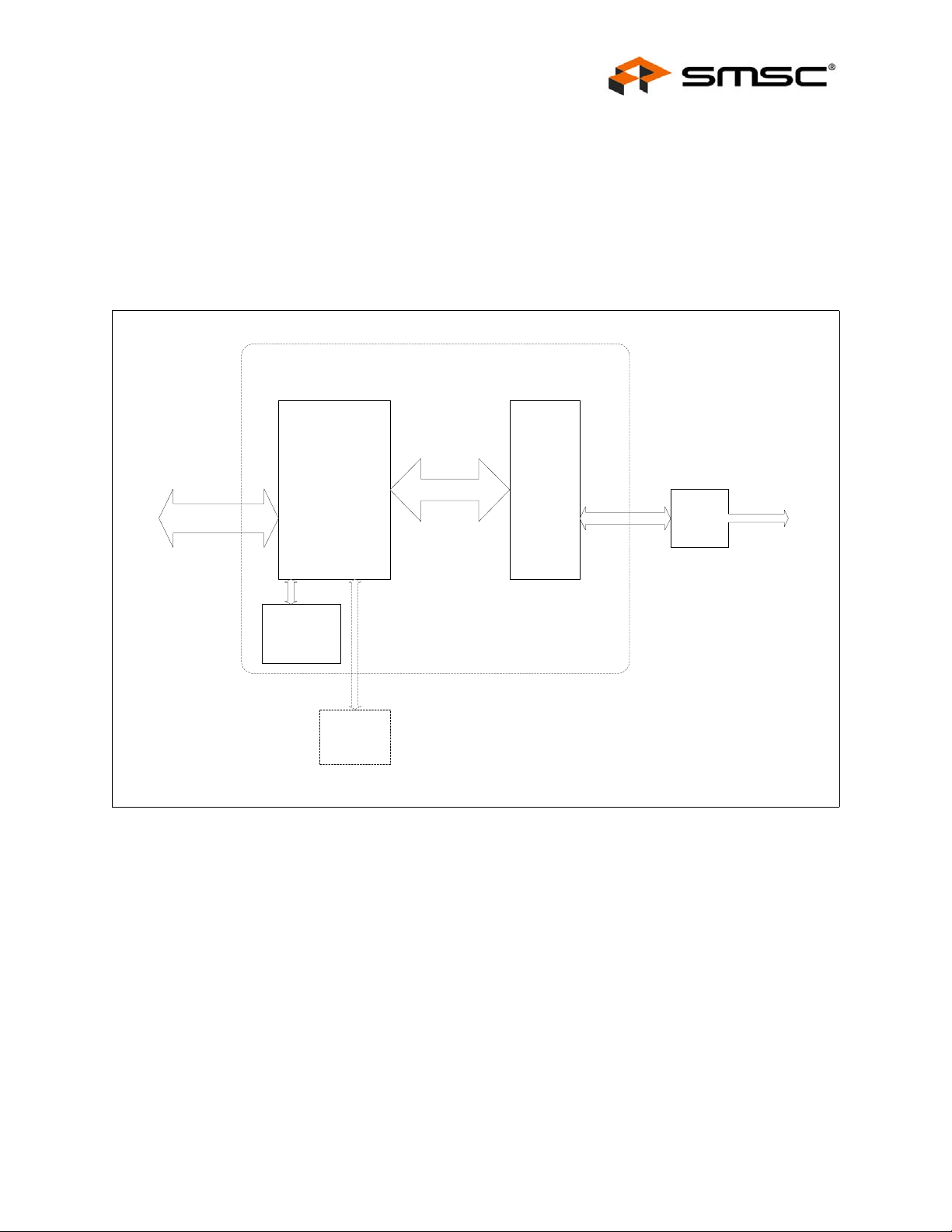
Chapter 3 Block Diagrams
The diagram shown in Figure 3.1, "Basic Functional Block Diagram", describes the device basic
functional blocks. The SMSC LAN91C111 is a single chip solution for embedded designs with minimal
Host and external supporting devices required to implement 10/100 Ethernet conne ctivity solutions.
The optional Serial EEPROM is used to store information relating to default IO offset parameters as
well as which of the Interrupt line are used by the ho st.
LAN91C111
ISA,Embedded
Processor
Host System
TX/RX Buffer (8K)
Ethernet
Internal IEEE 802.3 MII (Media
Independent Interface)
MAC
Serial
EEProm
(Optional)
Figure 3.1 Basic Functional Block Diagr am
PHY
Core
Transformer
Minimal LAN91C111
Configuration
RJ45
SMSC LAN91C111 REV C 11 Revision 1.91 (08-18-08)
DATASHEET
Page 12
10/100 Non-PCI Ethernet Single Chip MAC + PHY
Datasheet
Control
Address
Data
EEPROM
INTERFACE
8-32 bit
Bus
Interface
Unit
Control
Control
WR
FIFO
RD
FIFO
Control
Arbiter
MMU
8K Byte
Dynamically
Allocated
SRAM
Control
32-bit Data
32-bit Data
TX/RX
FIFO
Pointer
DMA
Control
TX Data
RX Data
Ethernet
Protocol
Handler
(EPH)
MII
Control
TPO
10/100
PHY
TXD[0-3]
TPI
RXD[0-3]
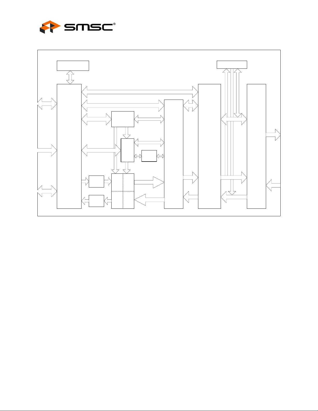
Figure 3.2 Block Diagram
The diagram shown in Figure 3.2 describes the supported Host interfaces, which include ISA or
Generic Embedded. The Host interface is an 8, 16 or 32 bit wide address / data bus with extensions
for 32, 16 and 8 bit embedded RISC and ARM processors.
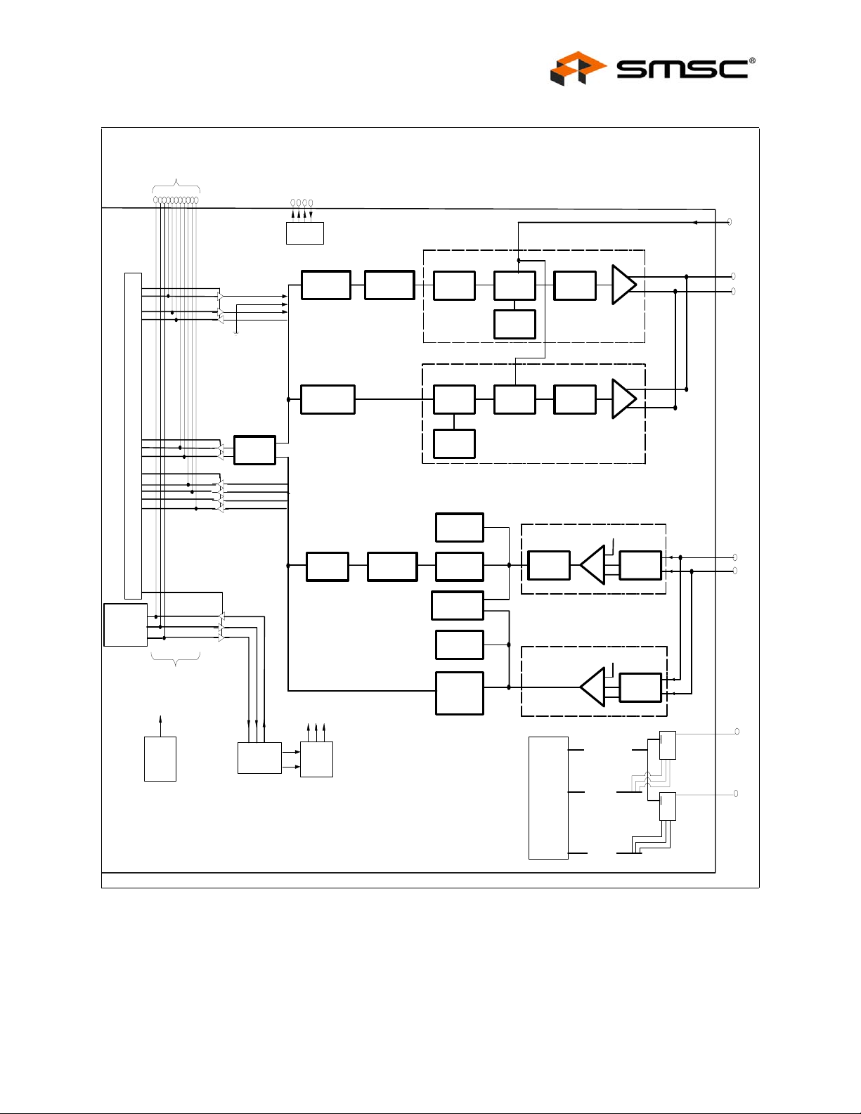
The figure shown next page describes the SMSC LAN91C111 functional blocks required to integrate
a 10/100 Ethernet Physical layer framer to the internal MAC.
Revision 1.91 (08-18-08) 12 SMSC LAN91C111 REV C
DATASHEET
Page 13
10/100 Non-PCI Ethernet Single Chip MAC + PHY
A
D
Datasheet
MII External
Signals
EECS
EESK
EEDO
EEDI
EEPROM
CONTROL
B
5
B
4
R
E
N
E
C
D
TXD[3:0]
TX_ER
TXEN100
TX25
O
S
A
B
I
R
X
T
E
-
B
A
S
0
0
1
E
R
T
T
I
S
M
A
N
R
T
T
C
H
D
E
I
W
E
M
B
L
A
R
S
C
M
R
R
E
N
E
C
D
O
T
-
S
E
0
B
A
1
E
T
R
T
I
M
S
A
N
R
T
N
E
T
C
U
R
R
E
O
R
U
S
C
C
K
L
O
C
E
N
G
L
)
P
L
(
S
3
L
T
P
L
E
T
L
I
F
+
-
R
+
P
O
T
-
P
O
T
MII
SERIAL
Manage
-ment
CSMA/CD
Power
Reset
On
MII
To MII External Signals
CRS100
COL100
RXD[3:0]
RX_ER
RX_DV
RX25
MDI
MCLK
MDO
L
O
L
C
CONTROLS
S
I
PHY
D
C
E
R
S
T
H
M
C
A
N
E
N
O
I
R
M
O
C
K
L
O
C
E
N
G
L
)
P
L
(
A
1
H
L
C
U
S
E
Q
&
C
K
O
L
4
D
C
E
AUTONEG
LOGIC
B
B
5
D
R
E
O
C
R
A
M
E
S
D
R
E
C
B
L
A
A
T
D
E
R
Y
V
O
E
C
R
T
U
O
A
N
E
N
G
O
I
A
T
T
I
O
K
&
N
L
I
H
L
C
U
S
E
Q
&
C
K
L
O
C
A
A
T
D
y
e
r
v
o
e
c
R
t
e
s
e
r
h
n
c
M
a
(
)
r
d
e
o
e
c
D
E
1
R
P
L
E
T
L
I
F
X
T
E
-
B
A
S
0
0
E
I
E
C
R
V
E
R
L
T
M
D
R
E
N
C
O
-
T
S
E
A
0
B
I
V
E
R
E
E
C
LED
Control
R
+
+
-
+
+
-
nPLED[0-5]
LS[2-0]A
+
-
h
V
t
-
+
/
I
+
P
V
E
P
T
I
A
A
D
L
I
R
Z
E
U
E
A
Q
h
V
t
-
+
/
P
L
E
T
R
L
I
F
Multiplex er
S
D
1
S
8
EN
C
C
1
3C2
B
Multiplex er
S
D
1
S
8
EN
C
C
1
3C2
B
T
P
I
T
-
LED
LE
LS[2-0]B
Figure 3.3 LAN91C111 Physical Layer to Internal MAC Block Diagram
SMSC LAN91C111 REV C 13 Revision 1.91 (08-18-08)
DATASHEET
Page 14

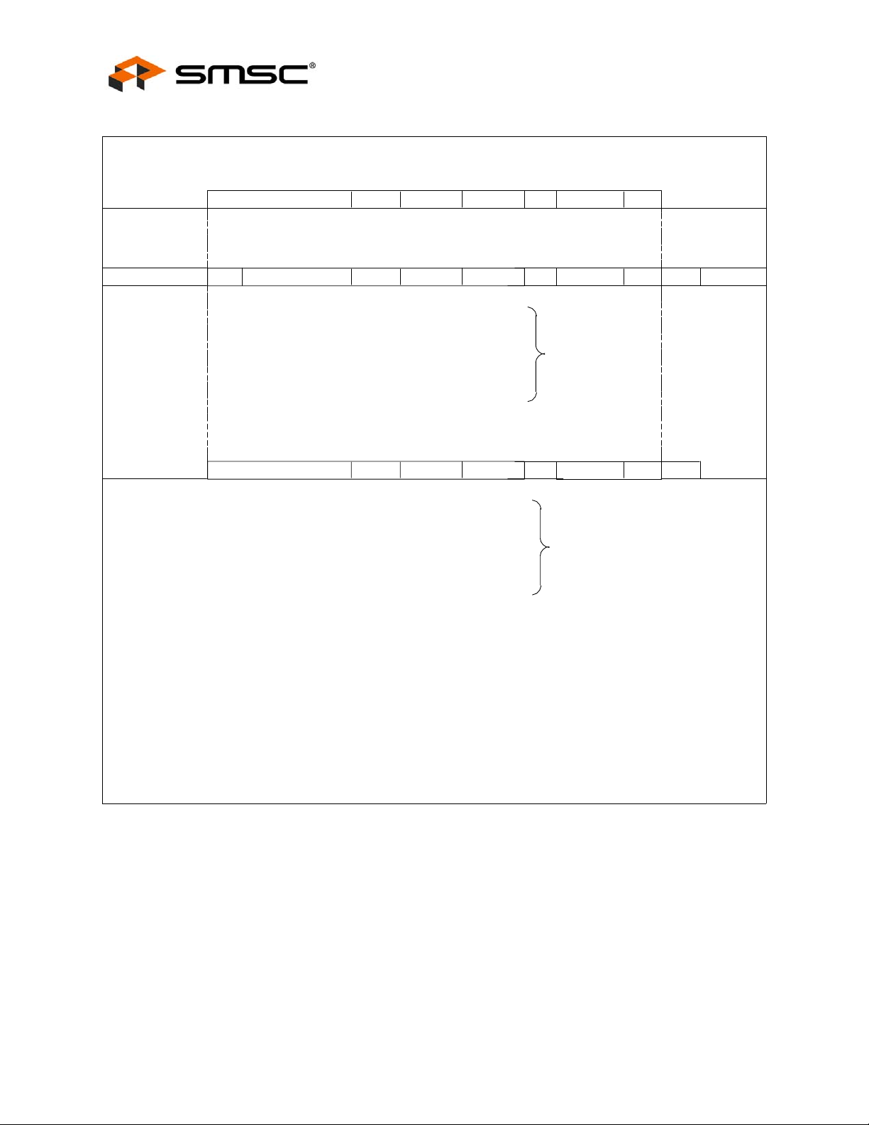
Chapter 4 Signal Descriptions
Table 4.1 LAN91C111 Pin Requirements (128 Pin QFP and 1.0mm TQFP package)
FUNCTION PIN SYMBOLS NUMBER OF PINS
System Address Bus A1-A15, AEN, nBE0-nBE3 20
System Data Bus D0-D31 32
10/100 Non-PCI Ethernet Single Chip MAC + PHY
Datasheet
System Control Bus RESET, nADS, LCLK, ARDY,
nRDYRTN, nSRDY, INTR0, nLDEV,
nRD, nWR, nDATACS, nCYCLE, W/nR,
nVLBUS
Serial EEPROM EEDI, EEDO, EECS, EESK, ENEEP,
IOS0-IOS2
LEDs nLEDA, nLEDB 2
PHY TPO+, TPO-, TPI+, TPI-, nLNK, LBK,
nCNTRL, RBIAS
Crystal Oscillator XTAL1, XTAL2 2
Power VDD, AVDD 10
Ground GND, AGND 12
Physical Interface (MII) TXEN100, CRS100, COL100, RX_DV,
RX_ER, TXD0-TXD3, RXD0-RXD3,
MDI, MDO, MCLK, RX25, TX25
MISC nCSOUT, X25OUT 2
TOTAL 128
14
8
8
18
Revision 1.91 (08-18-08) 14 SMSC LAN91C111 REV C
DATASHEET
Page 15

10/100 Non-PCI Ethernet Single Chip MAC + PHY
Datasheet
Chapter 5 Description of Pin Functions
PIN NO.
NAME SYMBOL
TQFP QFP
81-92 83-94 Address A4-A15 I** Input. Decoded by LAN91C111 to
78-80 80-82 Address A1-A3 I** Input. Used by LAN91C111 for internal
41 43 Address Enable AEN I** Input. Used as an address qualifier.
94-97 96-99 nByte Enable nBE0-
107-104,
102-99, 7673, 71-68,
66-63, 6158, 56-53,
51-48
30 32 Reset RESET IS** Input. When this pin is asserted high, the
109-106,
104-101,
78-75, 7370, 68-65,
63-60, 5855, 53-50
Data Bus D0-D31 I/O24** Bidirecti onal. 32 bit data bus used to
nBE3
BUFFER
TYPE
I** Input. Used during LAN91C111 register
DESCRIPTION
determine access to its registers.
register selection.
Address decoding is only enabled when
AEN is low.
accesses to determine the width of the
access and the register(s) being
accessed. nBE0-nBE3 are ignored when
nDATACS is low (burst accesses)
because 32 bit transfers are assumed.
access the LAN91C111’s internal
registers. Data bus has weak internal
pullups. Supports direct connection to the
system bus without external buffering.
For 16 bit systems, only D0-D15 are
used.
controller performs an internal system
(MAC & PHY) reset. It programs all the
registers to their default value, the
controller will read the EEPROM device
through the EEPROM interface
This input is not considered active unless
it is active for at least 100ns to filter
narrow glitches.
(Note 5.1).
37 39 nAddress
Strobe
35 37 nCycle nCYCLE I** Input. This active l ow signal is used to
36 38 Write/
nRead
40 42 nVL Bus Access nVLBUS I with
SMSC LAN91C111 REV C 15 Revision 1.91 (08-18-08)
nADS IS** Input. For systems that require address
W/nR IS** Input. Defines th e direction of
pullup**
latching, the rising edge of nADS
indicates the latching moment for A1-A15
and AEN. All LAN91C111 internal
functions of A1-A15, AEN are latched
except for nLDEV decoding.
control LAN91C111 EISA burst mode
synchronous bus cycles.
synchronous cycles. Write cycles when
high, read cycles when low.
Input. When low, the LAN91C111
synchronous bus interface is configured
for VL Bus accesses. Otherwise, the
LAN91C111 is configured for EISA DMA
burst accesses. Does not affect the
asynchronous bus interface.
DATASHEET
Page 16

10/100 Non-PCI Ethernet Single Chip MAC + PHY
Datasheet
PIN NO.
NAME SYMBOL
TQFP QFP
BUFFER
TYPE
DESCRIPTION
42 44 Local Bus Clock LCLK I** Input. Used to interface synchronous
buses. Maximum frequency is 50 MHz.
Limited to 8.33 MHz for EISA DMA burst
mode. This pin should be tied high if it is
in asynchronous mode.
38 40 Asynchronous
Ready
ARDY OD16 Open drain output. ARDY may be used
when interfacing asynchronous buses to
extend accesses. Its rising (access
completion) edge is controlled by the
XTAL1 clock and, therefore,
asynchronous to the host CPU or bus
clock. ARDY is negated during
Asynchronous cycle when one of the
following conditions occurs:
No_Wait Bit in the Configuration Register
is cleared.
Read FIFO contains less than 4 bytes
when read.
Write FIFO is full when write.
43 45 nSynchronous
Ready
nSRDY O16 Output. This output is used when
interfacing synchronous buses and
nVLBUS=0 to extend accesses. This
signal remains normally inactive, and its
falling edge indicates completion. This
signal is synchronous to the bus clock
LCLK.
46 48 nReady Return nRDYRTN I** Input. This input is used to complete
synchronous read cycles. In EISA burst
mode it is sampled on falling LCLK
edges, and synchronous cycles are
delayed until it is sampled high.
29 31 Interrupt INTR0 O24 Interrupt Output – Active High, it’s used to
interrupt the Host on a status event.
Note: The selection bits used to
determined by the value of INT SEL 1-0
bits in the Configuration Register are no
longer required and have been set to
reserved in this revision of the FEAST
family of devices.
45 47 nLocal Device nLDEV O16 Output. This active low output is asserted
when AEN is low and A4-A15 decode to
the LAN91C111 address programmed
into the high byte of the Base Address
Register. nLDEV is a combinatorial
decode of unlatched address and AEN
signals.
31 33 nRead Strobe nRD IS** Input. Used in asyn chronous bus
interfaces.
32 34 nWrite Strobe nWR IS** Input. Used in a synchronous bus
interfaces.
34 36 nData Path
Chip Select
nDATACS I with
pullup**
Input. When nDATACS is low, the Data
Path can be accessed regardless of the
values of AEN, A1-A15 and the content of
the BANK SELECT Register. nDATACS
provides an interface for bursting to and
from the LAN91C111 32 bits at a time.
Revision 1.91 (08-18-08) 16 SMSC LAN91C111 REV C
DATASHEET
Page 17

10/100 Non-PCI Ethernet Single Chip MAC + PHY
Datasheet
PIN NO.
NAME SYMBOL
TQFP QFP
BUFFER
TYPE
DESCRIPTION
9 11 EEPROM Clock EESK O4 Output. 4 μsec clock used to shift data in
and out of the serial EEPROM.
10 12 EEPROM
Select
EECS O4 Output. Serial EEPROM chip select.
Used for selection and command framing
of the serial EEPROM.
7 9 EEPROM Data
Out
8 10 EEPROM Data InEEDI I with
3-5 5-7 I/O Base IOS0-IOS2 I with
EEDO O4 Output. Connected to the DI input of the
serial EEPROM.
Input. Connected to the DO output of the
pulldown **
serial EEPROM.
Input. External switches can be
pullup**
connected to these lines to select
between predefined EEPROM
configurations.
68Enable
EEPROM
ENEEP I with
pullup**
Input. Enables (when high or open)
LAN91C111 accesses to the serial
EEPROM. Must be grounded if no
EEPROM is connected to the
LAN91C111.
127, 128 1, 2 Crystal 1
Crystal 2
XTAL1
XTAL2
Iclk** An external 25 MHz crystal is connected
across these pins. If a TTL clock is
supplied instead, it should be connected
to XTAL1 and XTAL2 should be left open.
XTAL1 is the 5V tolerant input of the
internal amplifier and XTAL2 is the output
of the internal amplifier.
1, 33, 44,
62, 77, 98,
110, 120
3, 35, 46,
64, 79,
100, 112,
Power VDD +3.3V Power supply pins.
122
11, 16 13, 18 Analog Power AVDD +3.3V Analog power supply pins.
24, 39, 52,
57, 67, 72,
93, 103,
108, 117
26, 41, 54,
59, 69, 74,
95, 105,
110 , 11 9
Ground GND Ground pins.
13, 19 15, 21 Analog Ground AGND Analog Ground pins
21 23 Loopback LBK O4 Outp ut. Active when LOOP bit is set
(TCR bit 1).
20 22 nLink Status nLNK I with
pullup
Input. General-purpose input port used to
convey LINK status (EPHSR bit 14).
28 30 nCNTRL nCNTRL O12 General Purpose Control Pin
47 49 X25out X25out O12 25Mhz Output to external PHY
111 113 Transmit Enable
100 Mbps
119 121 Carrier Sense
100 Mbps
TXEN100 O12 Output to MII PHY. Envelope to 100
Mbps transmission.
CRS100 I with
pulldown
Input from MII PHY. Envelope of packet
reception used for deferral and backoff
purposes.
SMSC LAN91C111 REV C 17 Revision 1.91 (08-18-08)
DATASHEET
Page 18

10/100 Non-PCI Ethernet Single Chip MAC + PHY
Datasheet
PIN NO.
NAME SYMBOL
TQFP QFP
125 127 Receive Data
RX_DV I with
Valid
112 114 Collision Detect
COL100 I with
100 Mbps
113-116 115-118 Transmit Data TXD3-
BUFFER
TYPE
pulldown
pulldown
O12 Outputs. Transmit Data nibble to MII
TXD0
109 111 Transmit Clock TX25 I with
pullup
118 120 Receive Clock RX25 I with
pullup
121-124 123-126 Receive Data RXD3-
RXD0
25 27 Management
MDI I with
Data Input
26 28 Management
MDO O4 MII management d ata output.
I with
pullup
pulldown
Data Output
DESCRIPTION
Input from MII PHY. Envelope of data
valid reception. Used for receive data
framing.
Input from MII PHY. Collision detection
input.
PHY.
Input. Transmit clock input from MII.
Nibble rate clock (25MHz for 100Mbps &
2.5MHz for 10Mbps).
Input. Receive clock input from MII PHY.
Nibble rate clock. (25MHz for 100Mbps &
2.5MHz for 10Mbps).
Inputs. Received Data nibble from MII
PHY.
MII management data input.
27 29 Management
MCLK O4 MII management cl ock.
Clock
126 128 Receive Error RX_ER I with
pulldown
Input. Indicates a code error detected by
PHY. Used by the LAN91C111 to discard
the packet being received. The error
indication reported for this event is the
same as a bad CRC (Receive Status
Word bit 13).
2 4 nChip Select
Output
nCSOUT O4 Outp ut. Chip Select provided for
mapping of PHY functions into
LAN91C111 decoded space. Active on
accesses to LAN91C111’s eight lower
addresses when the BANK SELECTED is
7.
12 14 External
Resistor
RBIAS NA Transmit Current Set. An external
resistor connected between this pin and
GND will set the output current for the TP
transmit outputs
14 16 TPO+ O/I Twisted Pair Transmit Output, Positive.
15 17 TPO- O/I Twisted Pair Transmit Output, Negative
17 19 TPI+ I/O Twisted Pair Receive Input, Positive
18 20 TPI- I/O Twisted Pair Receive Input, Negative.
22 24 nLEDA OD24 PHY LED Output
23 25 nLEDB OD24 PHY LED Output
Note 5.1 If the EEPROM is enabled.
Revision 1.91 (08-18-08) 18 SMSC LAN91C111 REV C
DATASHEET
Page 19

10/100 Non-PCI Ethernet Single Chip MAC + PHY
Datasheet
Chapter 6 Signal Description Parameters
This section provides a detailed description of each SMSC LAN91C111 signal. The signals are
arranged in functional groups according to their associated function.
The ‘n’ symbol at the beginning of a signal name indicates that it is an active low signal. When ‘n’ is
not present before the signal name, it indicates an active high signal.
The term “assert” or “assertion” indicates that a signal is active; i ndependent of whether that level is
represented by a high or low voltage. The term negates or negation indicates that a signa l is inactive.
The term High-Z means tri-stated.
The term Undefined means the signal could be high, low, tri-stated, or in some in-between level.
6.1 Buffer Types
O4 Output buffer with 2mA source and 4mA sink
O12 Output buffer with 6mA source and 12mA sink
O16 Output buffer with 8mA source and 16mA sink
O24 Output buffer with 12mA source and 24mA sink
OD16 Open drain buffer with 16mA sink
OD24 Open drain buffer with 24mA sink
I/O4 Bidirectional buffer with 2mA source and 4mA sink
I/O24 Bidirectional buffer with 12mA source and 24mA sink
I/OD Bidirectional Open drain buffer with 4mA sink
I Input buffer
IS Input buffer with Schmitt Trigger Hysteresis
Iclk Clock input buffer
I/O Differential Input
O/I Differential Output
** 5V tolerant. Input pins are able to accept 5V signals
DC levels and conditions defined in the DC Electrical Characteristics section.
SMSC LAN91C111 REV C 19 Revision 1.91 (08-18-08)
DATASHEET
Page 20

Chapter 7 Functional Description
7.1 Clock Generator Block
1. The XTAL1 and XTAL2 pins are to be connected to a 25 MHz crystal.
2. TX25 is an input clock. It will be the nibble rate of the particular PHY connected to the MII (2.5
MHz for a 10 Mbps PHY, and 25 MHz for a 100 Mbps PHY).
3. RX25 - This is the MII nibble rate receive clock used for sampling received data nibbles and
running the receive state machine. (2.5 MHz for a 10 Mbps PHY, and 25 MHz for a 100 Mbps PHY).
4. LCLK - Bus clock - Used by the BIU for synchronous accesses. Maximum frequency is 50 MHz
for VL BUS mode, and 8.33 MHz for EISA slave DMA.
7.2 CSMA/CD Block
This is a 16 bit oriented block, with fully- independent Transmit and Receive logic. The data path in
and out of the block consists of two 16-bit wide uni-directional FIFOs interfacing the DMA block. The
DMA port of the FIFO stores 32 bits to exploit the 32 bit data path into memory, but the FIFOs
themselves are 16 bit wide. The Control Path consists of a set of registers interfaced to the CPU via
the BIU.
10/100 Non-PCI Ethernet Single Chip MAC + PHY
Datasheet
7.2.1 DMA Block
This block accesses packet memory on the CSMA/CD’s behalf, fetching transmit data and storing
received data. It interfaces the CSMA/CD Transmit and Receive FIFOs on one side and the Arbiter
block on the other. To increase the bandwidth into memory, a 50 MHz clock is used by the DMA block,
and the data path is 32 bits wide.
For example, during active reception at 100 Mbps, the CSMA/CD block will write a word into the
Receive FIFO every 160ns. The DMA will read the FIFO and accumulate two words on the output port
to request a memory cycle from the Arbiter every 320ns.
The DMA machine is able to support full duplex operation. Independe nt receive and transmit counters
are used. Transmit and receive cycles are alternated when simultaneous receive and transmit
accesses are needed.
7.2.2 Arbiter Block
The Arbiter block sequences accesses to packet RAM requested by the BIU and by the DMA blocks.
BIU requests represent pipelined CPU accesses to the Data Register, while DMA requests represent
CSMA/CD data movement.
Internal SRAM read accesses are always 32 bit wide, and the Arbiter steers the appropriate byte(s) to
the appropriate lanes as a function of the address.
The CPU Data Path consists of two uni-directional FIFOs mapped at the D ata Register locatio n. These
FIFOs can be accessed in any combination of bytes, word, or doublewords. The Arbiter will indicate
'Not Ready' whenever a cycle is initiated that cannot be satisfied by the present state of the FIFO.
7.3 MMU Block
The Hardware Memory Management Unit allocates memory and transmit and receive packet queues.
It also determines the value of the transmit and receive interrupts as a function of the queues. The
page size is 2048 bytes, with a maximum memory size of 8kbytes. MIR values are interpreted in 2048
byte units.
Revision 1.91 (08-18-08) 20 SMSC LAN91C111 REV C
DATASHEET
Page 21

10/100 Non-PCI Ethernet Single Chip MAC + PHY
Datasheet
7.4 BIU Block
The Bus Interface Unit can handle synchronous as well as asynchronous buses; different signals are
used for each one. Transparent latches are added on the address path using rising nADS for latching.
When working with an asynchronous bus like ISA, the read and write operations are controlled by the
edges of nRD and nWR. ARDY is used for notifying the system that it should extend the access cycle.
The leading edge of ARDY is generated by the leading ed ge of nRD or nWR while the trailing edge
of ARDY is controlled by the internal LAN91C111 clock and, therefore, asynchronous to the bus.
In the synchronous VL Bus type mode, nCYCLE and LCLK are used to for read and write operations.
Completion of the cycle may be determined by using nSRDY. nSRDY is controlled by LCLK and
synchronous to the bus.
Direct 32 bit access to the Data Path is supported by using the nDATACS input. By asserting
nDATACS, external DMA type of devices will bypass the BIU address decoders and can sequentially
access memory with no CPU intervention. nDATACS accesses can be used in the EISA DMA burst
mode (nVLBUS=1) or in asynchronous cycles. These cycles MUST be 32 bit cycles. Please refer to
the corresponding timing diagrams for details on these cycles.
The BIU is implemented using the following principles:
a. Address decoding is based on the values of A15-A4 and AEN.
b. Address latching is performed by using transparent latches that are transparent when nADS=0 and
nRD=1, nWR=1 and latch on nADS rising edge.
c. Byte, word and doubleword accesses to all registers and Data Path are supported except a
doubleword write to offset Ch will only write the BANK SELECT REGISTER (offset 0x0Fh).
d. No bus byte swapping is implemented (no eight bit mode).
e. Word swapping as a function of A1 i s implemented for 16 bit bus support.
f. The asynchronous interface uses nRD and nWR strobes. If necessary, ARDY is negated on the
leading edge of the strobe. The ARDY trailing edge is controlled by CLK.
g. The VLBUS synchronous interface uses LCLK, nADS, and W/nR as defined in the VESA
specification as well as nCYCLE to control read and write operations an d generate nSRDY.
h. EISA burst DMA cycles to and from the DATA REGISTER are supported as defined in the EISA
Slave Mode "C" specification when nDATACS is driven by nDAK.
i. Synchronous and asyn chrono us cycles can be mi xed as long a s they are not active simul taneously.
j. Address and bank selection can be bypassed to generate 32 bit Data Path accesses by activating
the nDATACS pin.
7.5 MAC-PHY Interface
The LAN91C111 integrates the IEEE 802.3 Physical Layer (PHY) and Media Access Control (MAC)
into the same silicon. The data path connection between the MAC and the internal PHY is provided
by the internal MII. The LAN91C111 also supports the EXT_PHY mode for the use of an external PHY,
such as HPNA. This mode isolates the internal PHY to allow interface with an external PHY through
the MII pins. To enter this mode, set EXT PHY bit to 1 in the Configuration Register.
7.5.1 Management Data Software Implementation
The MII interface contains of a pair of signals that physically transport the management informa tion
across the MII, a frame format and a protocol specification for exchanging management frames, and
a register set that can be read and written using these frames. MII management refers to the ability
of a management entity to communicate with PHY via the MII serial ma nagement interface (MI) for the
purpose of displaying, selecting and/or controlling different PHY options. The host manipulates the
MAC to drive the MII management serial interface. By manipulating the MAC's registers, MII
management frames are generated on the management interface for reading or writing information
from the PHY registers. Timing and framing for each management command is to be generated by
the CPU (host).
SMSC LAN91C111 REV C 21 Revision 1.91 (08-18-08)
DATASHEET
Page 22

The MAC and external PHY communicate via MDIO and MDC of the MII Management serial interface.
MDIO:Management Data input/output. Bi-directional between MAC and PHY that carries management
data. All control and status information sent over this pin is driven and sampled synchronously to the
rising edge of MDC signal.
MDC:Management Data Clock. Sourced by the MAC as a timing reference for transfer of information
on the MDIO signal. MDC is a periodic signal with no maximum h igh or low times. T he minimum high
and low times should be 160ns each and the minimum period of the signal shou ld be 400ns. These
values are regardless of the nominal period of the TX and RX clocks.
7.5.2 Management Data Timing
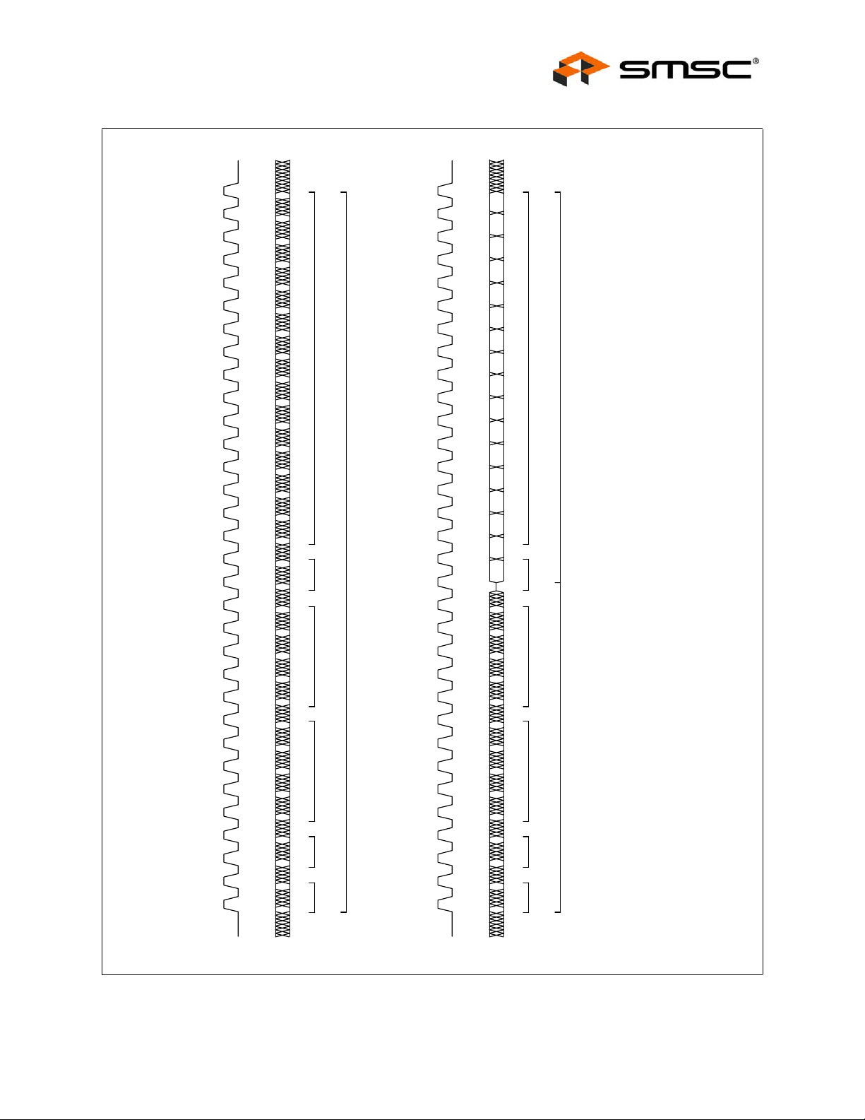
A timing diagram for a Ml serial port frame is shown in Figure 7.1. The Ml serial port is idle when at
least 32 continuous 1's are detected on MDIO and remains idle as long as continuous 1's are detected.
During idle, MDIO is in the high impedance state. When the Ml serial port is in the idle state, a 01
pattern on the MDIO initiates a serial shift cycle. Data on MDIO is then shifted in on the next 14 rising
edges of MDC (MDIO is high impedance). If the register access mode is not enabled, on the next 16
rising edges of MDC, data is either shifted in or out on MDIO, depending on whether a write or re ad
cycle was selected with the bits READ and WRITE. After the 32 MDC cycles have been completed,
one complete register has been read/written, the serial sh ift process is halted, data is latched into the
device, and MDIO goes into high impedance state. Another serial shift cycle cannot be initiated until
the idle condition (at least 32 continuous 1's) is detected.
10/100 Non-PCI Ethernet Single Chip MAC + PHY
Datasheet
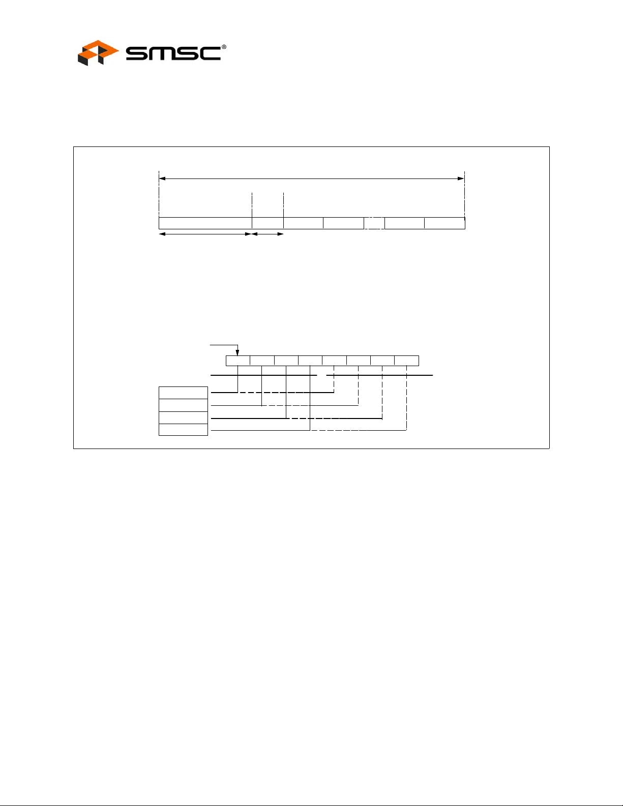
7.5.3 MI Serial Port Frame Structure
The structure of the PHY serial port frame is shown in Table 9.1 and timing diagram of a frame is
shown in Figure 7.1. Each serial port access cycl e consists of 32 bits (or 192 bits if multiple register
access is enabled and REGAD[4:0]=11111 ) , e x c l u s i v e o f i d l e . T h e f i r s t 1 6 b i t s o f t h e s e r i a l p o r t cycle
are always write bits and are used for addressing. The last 16/176 bits are from one/all of the 11 data
registers.
The first 2 bit in Table 9.1and Figure7.1 are start bits and need to be wr itten as a 01 for the serial po rt
cycle to continue. The next 2 bits are a read and write bit which determine if the accessed data register
bits will be read or write. The next 5 bits are device addresses. The next 5 bits are register address
select bits, which select one of the five data registers for access. The next 1 bit is a turnaround bit
which is not an actual register bit but extra time to switch MDIO from write to read if ne cessary, as
shown in Figure 7.1. The final 16 bits of the PHY Ml serial port cycle (or 176 bits if multiple register
access is enabled and REGAD[4:0]=11111) come from the specific data register designated by the
register address bits REGAD[4:0].
Revision 1.91 (08-18-08) 22 SMSC LAN91C111 REV C
DATASHEET
Page 23
10/100 Non-PCI Ethernet Single Chip MAC + PHY
Datasheet
1
3
0
3
9
2
8
2
7
2
6
2
5
2
4
2
3
2
2
2
1
2
0
2
9
1
8
1
7
1
6
1
5
1
4
1
3
1
2
1
1
1
0
1
9
8
7
6
5
4
3
2
1
E
0
L
C
Y
C
E
T
I
R
W
C
D
M
0
D
1
D
2
D
3
D
4
D
5
D
6
D
7
]
D
0
:
5
1
[
A
8
T
D
A
D
9
D
0
1
D
1
1
D
2
1
D
3
1
D
4
1
D
5
1
D
]
0
0
:
1
[
A
T
1
0
R
1
R
]
0
:
4
[
2
D
R
A
G
E
R
3
R
4
R
0
P
1
P
]
0
:
4
[
D
2
A
P
Y
H
P
3
P
4
P
1
]
0
:
1
[
P
O
0
1
]
0
:
1
[
T
S
0
O
I
D
M
C
D
M
F
O
S
E
G
D
E
G
N
I
S
I
E
R
S
T
I
T
N
I
R
B
O
W
A
T
A
D
N
I
S
K
C
O
L
C
Y
H
P
1
3
0
3
9
2
8
2
7
2
6
2
5
2
4
2
3
2
2
2
1
2
0
2
9
1
8
1
7
1
6
1
5
1
4
1
3
1
2
1
1
1
0
1
9
8
7
6
5
4
3
2
1
0
E
L
C
Y
C
D
A
E
R
C
D
M
0
D
1
D
2
D
3
D
4
D
5
D
6
D
7
D
8
D
9
D
0
1
D
1
1
D
2
1
D
3
1
D
4
1
D
5
1
D
0
Z
0
R
1
R
2
R
3
R
4
R
0
P
1
P
]
0
:
4
[
2
D
P
A
Y
H
P
3
P
4
P
0
]
0
:
1
[
P
O
1
1
]
0
:
1
[
T
S
0
O
I
D
M
C
D
M
F
O
S
E
G
D
E
G
N
I
S
S
I
T
]
R
I
0
B
:
N
5
D
O
1
[
A
A
A
E
T
T
R
A
A
D
D
T
U
O
S
K
C
O
L
C
Y
H
P
]
0
:
1
[
A
T
]
0
:
4
[
D
A
G
E
R
C
D
M
F
O
S
E
G
D
E
G
N
I
S
I
E
R
S
T
I
T
N
I
R
B
O
W
A
T
A
D
N
I
S
K
C
O
L
C
Y
H
P
Figure 7.1 MI Serial Port Frame Timing Diagra m
SMSC LAN91C111 REV C 23 Revision 1.91 (08-18-08)
DATASHEET
Page 24
10/100 Non-PCI Ethernet Single Chip MAC + PHY
7.5.4 MII Packet Data Communication with External PHY
The MIl is a nibble wide packet data interface defined in IEEE 802.3. The LAN91C111 meets all the
MIl requirements outlined in IEEE 802.3 and shown in Figure 7.2.
Datasheet
TX_EN = 0
IDLE
MII
NIBBLE
STREAM
PREAMBLE
PRMBLE
FIRST BIT
FIRST
NIBBLE
TXD0 / RXD0
TXD1 / RXD1
TXD2 / RXD2
TXD3 / RXD3
TX_EN = 1
OF
SFD
DATA 1
2 BT
= [ 1 0 1 0 ... ] 62 BITS LONG
= [ 1 1 ]
= [ BETWEEN 64-1518 DATA BYTES ]
MAC's SERIAL BIT STREAM
DATA NIBBLES
DATA 2
DATA N-1 DATA N
62 BT
LSB
START
FRAME
DELIM.
PREAMBLE
SFD
DATAn
IDLE = TX_EN = 0
D0 D1 D2 D3 D4 D5 D6 D7
Figure 7.2 MII Frame Format & MII Nibble Order
TX_EN = 0
IDLE
MSB
SECOND
NIBBLE
The Mll consists of the following signals: four transmit data bits (TXD[3:0]), transmit clock
(TX25),transmit enable (TXEN100), four receive data bits(RXD[3:0]), receive clock(RX25), carrier
sense (CRS100), receive data valid (RX_DV), receive data error (RX_ER), and collision (COL100).
Transmit data is clocked out using the TX25 clock input, while receive data is clocked in using RX25. Th e
transmit and receive clocks operate at 25 MHz in 100Mbps mode and 2.5 MHz in 10Mbps.
In 100 Mbps mode, the LAN91C111 provides the following interface signals to the PHY:
For transmission: TXEN100, TX D0-3, TX25
For reception: RX_DV, RX_ER, RXD0-3, RX25
For CSMA/CD state machines: CRS100, COL100
A transmission begins by TXEN100 going active (high), and TXD0-TXD3 having the first valid
preamble nibble. TXD0 carries the least significant bit of the nibble (that is the one tha t would go first
out of the EPH at 100 Mbps), while TXD3 carries the most significant bit of the nibble. TXEN100 and
TXD0-TXD3 are clocked by the LAN91C111 using TX25 rising edges. TXEN100 goe s inactive at the
end of the packet on the last nibble of the CRC.
During a transmission, COL100 might become active to indicate a collision. COL100 is asynchronous
to the LAN91C111’s clocks and will be synchronized internally to TX25.
Reception begins when RX_DV (receive data valid) is asserted. A preamble pattern or flag octet will
be present at RXD0-RXD3 when RX_DV is activated. The LAN91C111 requires no training sequence
beyond a full flag octet for reception. RX_DV as well as RXD0-RXD3 are sampled on RX25 rising
Revision 1.91 (08-18-08) 24 SMSC LAN91C111 REV C
DATASHEET
Page 25

10/100 Non-PCI Ethernet Single Chip MAC + PHY
Datasheet
edges. RXD0 carries the least significant bit and RXD3 the most significant bit of the nibble. RX_DV
goes inactive when the last valid nibble of the packet (CRC) is presented at RXD0-RXD3.
RX_ER might be asserted during packet reception to signal the L AN91C111 that the present receive
packet is invalid. The LAN91C111 will discard the packet by treating it as a CRC error.
RXD0-RXD3 should always be aligned to packet nibbles, therefore, opening flag d etection does not
consider misaligned cases. Opening flag detection expects the 5Dh pattern and will not reject the
packet on non-preamble patterns.
CRS100 is used as a frame envelope signal for the CSMA/CD MAC state machines (deferral and
backoff functions), but it is not used for receive framing functions. CRS100 is an asynchronous signal
and it will be active whenever there is activity on the cable, including LAN9 1C111 transmissions and
collisions.
7.6 Serial EEPROM Interface
This block is responsible for reading the serial EEPROM upon hardware reset (or equivalent
command) and defining defaults for some key registers. A write operation is also implemented b y this
block, that under CPU command will program specific locations in the EEPROM. This block is an
autonomous state machine and controls the internal Data Bus of the LAN91C111 during active
operation.
7.7 Internal Physical Layer
The LAN91C111 integrates the IEEE 802.3 physical layer (PHY) internally. The EXT PHY bit in the
Configuration Register is 0 as the default configuration to set the internal PHY enabled. The internal
PHY address is 00000, the driver must use this address to talk to the internal PHY. The inte rnal PHY
is placed in isolation mode at power up and reset. It can be removed from isolation mode by clearing
the MII_DIS bit in the PHY Control Register. If necessary, the internal PHY can be enabled by clearing
the EXT_PHY bit in the Configuration Register.
The internal PHY of LAN91C111 has nine main sections: controller interface, encoder, decoder,
scrambler, descrambler, clock and data recovery, twisted pair transmitter, twisted pair receiver, and MI
serial port.
The LAN91C111 can operate as a 100BASE-TX device (hereafter referred to as 100Mbps mode) or
as a 10BASE-T device (hereafter referred to as 10Mbps mode). The difference between the 100Mbps
mode and the 10Mbps mode is data rate, signaling protocol, and allowed wiring. The 100Mbps TX
mode uses two pairs of category 5 or better UTP or STP twisted pair cable with 4B5B encoded,
scrambled, and MLT-3 coded 62.5 MHz ternary data to achieve a throughput of 100Mbps. The 10Mbps
mode uses two pairs of category 3 or better UTP or STP twisted pair cable with Manchester encoded,
10MHz binary data to achieve a 10Mbps throughput. The data symbol format on the twisted pair cable
for the 100 and 10Mbps modes are defined in IEEE 802.3 specifications and shown in Figure 7.3.
SMSC LAN91C111 REV C 25 Revision 1.91 (08-18-08)
DATASHEET
Page 26
10/100 Non-PCI Ethernet Single Chip MAC + PHY
Datasheet
INTERFRAME
GAP
IDLE
IDLE
PREAMBLE
SSD
DA, SA, LN, LLC DATA, FCS
PREAMBLE
PREAMBLE
DA, SA, LN, LLC DATA, FCS
PREAMBLE
IDLE
PREAMBLE
SFD
= [ 1 1 ] WITH NO MID BIT TRANSITION
SOI
ETHERNET MAC
FRAME
SFD DA
100 BASE-TX DATA SYMBOL S
SFD
IDLE
SSD
= [ 1 1 0 0 0 1 0 0 0 1]
= [ 1 0 1 0 ...] 62 BITS LONG
SFD
= [ 1 1]
= [ DATA]
= [ 0 1 1 0 1 0 0 1 1 1]
ESD
10 BASE-T DATA SYMBOLS
SFD
= [ NO TRANSITIONS]
= [ 1 0 1 0 ... ] 62 BITS LONG
= [ 1 1]
= [ DATA]
DA
= [ 1 1 1 1...]
DA
SA
SA
SA
LN
LLC DATA
LN ESD
LLC DATA
BEFORE / AFTER
4B5B ENCODING,
SCRAMBLING,
AND MLT3
CODING
LN
LLC DATA
BEFORE / AFTER
MANCHESTER
ENCODING
FCS
FCS
FCS
SOI
INTERFRAME
GAP
IDLE
IDLE
Figure 7.3 TX/10BT Frame Format
On the transmit side for 100Mbps TX operation, data is received on the controller and then se nt to the
4B5B encoder for formatting. The encoded data is then sent to the scrambler. The scrambled and
encoded data is then sent to the TP transmitter. The TP transmitter converts the encoded and
scrambled data into MLT-3 ternary format, reshapes the output, and drives the twisted pair cable.
On the receive side for 100Mbps TX operation, the twisted pair receiver receives incoming e ncoded
and scrambled MLT-3 data from the twisted pair cable, remove any h igh frequency noise, equalizes
the input signal to compensate for the effects of the cabl e, qualifies the data with a squelch algorithm,
and converts the data from MLT-3 coded twisted pair levels to internal digital levels. The output of the
twisted pair receiver then goes to a clock and data recovery block which recovers a clock from the
incoming data, uses the clock to latch in valid data into the devic e, and converts the data back to NRZ
format. The NRZ data is then unscrambled and decoded by the 4B5B decoder and descrambler,
respectively, and outputted to the Ethernet controller.
Revision 1.91 (08-18-08) 26 SMSC LAN91C111 REV C
DATASHEET
Page 27

10/100 Non-PCI Ethernet Single Chip MAC + PHY
Datasheet
10Mbps operation is similar to the 100Mbps TX operation except, (1) there is no
scrambler/descrambler, (2) the encoder/decoder is Manchester instead of 4B5B, (3) the data rate is
10Mbps instead of 100Mbps, and (4) the twisted pair symbol data is two level Manche ster instead of
ternary MLT-3.
The Management Interface, (hereafter referred to as the MI serial port), is a two pin bi-directional link
through which configuration inputs can be set and status outputs can be read. Each block plus the
operating modes are described in more detail in the following sections.
7.7.1 MII Disable
The internal PHY MII interface can be disabled by setting the MII disable bit in the MI serial port Control
register. When the MII is disabled, the MII inputs are ignored, the MII outputs are placed in high
impedance state, and the TP output is high impedance.
7.7.2 Encoder
4B5B Encoder - 100 Mbps
100BASE-TX requires that the data be 4B5B encoded. 4B5B coding converts the 4-Bit data nibbles
into 5-Bit date code words. The mapping of the 4B nibbles to the 5B code words is specified in IEEE
802.3. The 4B5B encoder on the LAN91C111 takes 4B nibbles from the controller interface, converts
them into 5B words and sends the 5B words to the scrambl er. The 4B5B encoder also substitutes the
first 8 bits of the preamble with the SSD delimiters (a.k.a. /J/K/ symbo ls) and adds an ESD delimiter
(a.k.a. MR/ symbols) to the end of every packet, as defined in IEEE 802.3. The 4B5B encoder also
fills the period between packets, called the idle period, with the continuou s stream of idle symbols.
Manchester Encoder - 10 Mbps
The Manchester encoding process combines clock and NRZ data such that the first half of the data
bit contains the complement of the data, and the second half of the data bit contains the true data, as
specified in IEEE 802.3. This guarantees that a transition always occurs in the middle of the bit call.
The Manchester encoder on the LAN91C111 converts the 10Mbps NRZ data from the controller
interface into a Manchester Encoded data stream for the TP transmitter and adds a start of idle pulse
(SOI) at the end of the packet as specified in IEEE 802.3. The Manchester encoding process is only
done on actual packet data, and the idle period between packets is not Manchester encoded and filled
with link pulses.
7.7.3 Decoder
4B5B Decoder - 100 Mbps
Since the TP input data is 4B5B encoded on the transmit side, it must also be decoded by the 4B5B
decoder on the receive side. The mapping of the 5B nibbles to the 4B code words i s specified in IEEE
802.3. The 4B5B decoder on the LAN91C111 takes the 5B code words from the descrambler, converts
them into 4B nibbles per Table 2, and sends the 4B nibbles to the controller interface. The 4B5B
decoder also strips off the SSD delimiter (a.k.a. /J/K/ symbols) and replaces them with two 4B Data 5
nibbles (a.k.a. /5/ symbol), and strips off the ESD delimiter (a.k.a. /T/R/ symbols) and replaces it with
two 4B Data 0 nibbles (a.k.a. /I/symbol), per IEEE 802.3 specifications and shown in Figure 7.3.
T a ble 7.1 4B/5B Symbol Mapping
SYMBOL NAME DESCRIPTION 5B CODE 4B CODE
0 Data 0 11110 0000
1 Data 1 01001 0001
2 Data 2 10100 0010
SMSC LAN91C111 REV C 27 Revision 1.91 (08-18-08)
DATASHEET
Page 28

10/100 Non-PCI Ethernet Single Chip MAC + PHY
Table 7.1 4B/5B Symbol Mapping (continued)
SYMBOL NAME DESCRIPTION 5B CODE 4B CODE
3 Data 3 10101 0011
4 Data 4 01010 0100
5 Data 5 01011 0101
6 Data 6 01110 0110
7 Data 7 01111 0111
8 Data 8 10010 1000
9 Data 9 10011 1001
A Data A 10110 1010
B Data B 10111 1011
C Data C 11010 1100
D Data D 11011 1101
Datasheet
E Data E 11100 1110
F Data F 11101 1111
I Idle 11111 0000
J SSD #1 11000 0101
K SSD #2 10001 0101
T ESD #1 01101 0 000
R ESD #2 00111 0000
H Halt 00100 Undefined
--- Invalid codes All others* 0000*
* These 5B codes are not used. For decod er, these 5B codes are decoded to 4B 0000. For encoder,
4B 0000 is encoded to 5B 11110, as shown in symbol Data 0.
The 4B5B decoder detects SSD, ESD and codeword errors in the incoming data stream as specified
in IEEE 802.3. These errors are indicated by asserting RX_ER output while the errors are being
transmitted across RXD[3:0], and they are also indicated in the serial port by setting SSD, ESD, and
codeword error bits in the PHY MI serial port Status Output register.
Manchester Decoder - 10 Mbps
In Manchester coded data, the first half of the data bit contains the complement of the data, and the
second half of the data bit contains the true data. The Manchester decoder in the LAN91C111 converts
the Manchester encoded data stream from the TP receiver into NRZ data for the controller interface
by decoding the data and stripping off the SOI pulse. Since the clock and data recovery block has
already separated the clock and data from the TP receiver, the Manchester decoding process to NRZ
data is inherently performed by that block.
Revision 1.91 (08-18-08) 28 SMSC LAN91C111 REV C
DATASHEET
Page 29

10/100 Non-PCI Ethernet Single Chip MAC + PHY
Datasheet
7.7.4 Clock and Data Recovery
Clock Recovery - 100 Mbps
Clock recovery is done with a PLL. If there is no vali d data present on the T P inputs, the PLL is locked
to the 25 MHz TX25. When valid data is detected on the TP inputs with the squelch circuit and when
the adaptive equalizer has settled, the PLL input is switch ed to the incoming data on the TP input.
The PLL then recovers a clock by locking onto the transitions o f the incoming signal from the twisted
pair wire. The recovered dock frequency is a 25 MHz nibble dock, and that clock is outputted on the
controller interface signal RX25.
Data Recovery - 100 Mbps
Data recovery is performed by latching in data from the TP receiver with the recovered clock extracted
by the PLL. The data is then converted from a single bit stream i nto nibble wide data word according
to the format shown in Figure 7.2.
Clock Recovery - 10 Mbps
The clock recovery process for 10Mbps mode is identical to the 100Mbps mode except, (1) the
recovered clock frequency is 2.5 MHz nibble clock, (2) the PLL is switched from TX25 to the TP input
when the squelch indicates valid data, (3) The PLL takes up to 12 transitions (bit times) to lock onto
the preamble, so some of the preamble data symbols are lost, but the dock recovery block recovers
enough preamble symbols to pass at least 6 nibbles of preamble to the receive controller interface as
shown in Figure 7.2.
Data Recovery - 10 Mbps
The data recovery process for 10Mbps mode is identical to the 100Mbps mode. As mentioned in the
Manchester Decoder section, the data recovery process inherently performs decoding of Manchester
encoded data from the TP inputs.
7.7.5 Scrambler
100 Mbps
100BASE-TX requires scrambling to reduce the radiated emissions on the twisted pair. The
LAN91C111 scrambler takes the encoded data from the 4B5B encoder, scrambles it per the IEEE
802.3 specifications, and sends it to the TP transmitter.
10 Mbps
A scrambler is not used in 10Mbps mode.
Scrambler Bypass
The scrambler can be bypassed by setting the bypass scrambler/descrambler bit in the PHY Ml serial
port Configuration 1 register. When this bit is set, the 5B data bypasses the scrambler and goes
directly from the 4B5B encoder to the twisted pair transmitter.
7.7.6 Descrambler
100 Mbps
The LAN91C111 descrambler takes the scrambled data from the data recovery block, descrambles it
per the IEEE 802.3 specifications, aligns the data on the correct 5B word boundaries, and sends it to
the 4B5B decoder.
The algorithm for synchronization of the descrambler is the same as the algorithm outli ned in the IEEE
802.3 specification. Once the descrambler is synchronized, i t will maintain synchronization as long as
enough descrambled idle pattern 1's are defected within a given interval. To stay in synchronization,
the descrambler needs to detect at least 25 consecutive descrambled idle pattern 1's in a 1ms interval.
SMSC LAN91C111 REV C 29 Revision 1.91 (08-18-08)
DATASHEET
Page 30

If 25 consecutive descrambled idle pattern 1's are not detected within the 1ms interval, the descrambler
goes out of synchronization and restarts the synchronization process.
If the descrambler is in the unsynchronized state, the descrambler loss of synchronization detect bit is
set in the Ml serial port Status Output register to indicate this condition. Once this bit is set, it will stay
set until the descrambler achieves synchronization.
10 Mbps
A descrambler is not used in 10 Mbps mode.
Descrambler Bypass
The descrambler can be bypassed by setting the bypass scrambler/descrambler bit in the PHY MI
serial port Configuration 1 register. When this bit is set, the data bypasses the descrambler and goes
directly from the TP receiver to the 4B5B decoder.
7.7.7 Twisted Pair Transmitter
Transmitter - 100 Mbps
The TX transmitter consists of MLT-3 encoder, waveform generator and line driver.
The MLT-3 encoder converts the NRZ data from the scrambler into a three level MLT-3 code required
by IEEE 802.3. MLT-3 coding uses three levels and converts 1's to transitions between the three levels,
and converts 0's to no transitions or changes in level.
10/100 Non-PCI Ethernet Single Chip MAC + PHY
Datasheet
The purpose of the waveform generator is to shape the transmit output pulse. The waveform generator
takes the MLT-3 three level encoded waveform and uses an array of switched current sources to
control the rise/fall time and level of the signal at the Output. The output of the switched current
sources then goes through a low pass filter in order to "smooth" the current output and remove any
high frequency components. In this way, the waveform generator preshapes the output waveform
transmitted onto the twisted pair cable to meet the pulse template requirements outlined in IEEE 802.3.
The waveform generator eliminates the need fo r any external filters on the TP transmit output.
The line driver converts the shaped and smoothed waveform to a curr ent output that can drive 100
meters of category 5 unshielded twisted pair cable or 150 Ohm shielded twisted pair cable.
Transmitter - 10 Mbps
The transmitter operation in 10 Mbps mode is much different than the 100 Mbps transmitter. Even so,
the transmitter still consists of a waveform generator and line driver.
The purpose of the waveform generator is to shape the output transmit pulse. The waveform generator
consists of a ROM, DAC, dock generator, and filter. The DAC generates a stair-stepped representation
of the desired output waveform. The stairstepped DAC output then goes thro ugh a low pass filter in
order to "smooth' the DAC output and remove any high frequency components. The DAC values are
determined from the ROM outputs; the ROM contents are chosen to shape the pulse to the desired
template and are clocked into the DAC at high speed by the clock generator. In this way, the waveform
generator preshapes the output waveform to be transmitted onto the twi sted pair cable to meet the
pulse template requirements outlined in IEEE 802.3 Clause 14 and also shown in Figure 7.4. The
waveshaper replaces and eliminates external filters on the T P transmit output.
The line driver converts the shaped and smoothed waveform to a curr ent output that can drive 100
meters of category 3/4/5 100 Ohm unshielded twisted pair cable or 150 Ohm shielded twisted pair
cable tied directly to the TP output pins without any extern al filters. During the idle period, no output
signal is transmitted on the TP outputs (except link pulse).
Revision 1.91 (08-18-08) 30 SMSC LAN91C111 REV C
DATASHEET
Page 31

10/100 Non-PCI Ethernet Single Chip MAC + PHY
Datasheet
1.0
0.8
0.6
0.4
0.2
)
0.0
V
(
e
g
-0.2
a
t
l
o
-0.4
V
-0.6
-0.8
-1.0
0 102030405060708090100110
B
H
D
C
A
E
F
G
I
M
K
L
N
P
O
Q
J
W
R
S
U
V
T
TIME (ns)
Figure 7.4 TP Output Voltage Template - 10 MBPS
REFERENCE TIME (NS) INTERNAL MAU VOLTAGE (V)
A00
B151.0
C150.4
D250.55
E320.45
F390
G57-1.0
H480.7
I670.6
J890
K74-0.55
L73-0.55
M610
N851.0
O1000.4
P 110 0.75
SMSC LAN91C111 REV C 31 Revision 1.91 (08-18-08)
DATASHEET
Page 32

10/100 Non-PCI Ethernet Single Chip MAC + PHY
Datasheet
REFERENCE TIME (NS) INTERNAL MAU VOLTAGE (V)
Q 111 0.15
R1110
S111-0.15
T110-1.0
U100-0.3
V110-0.7
W90-0.7
Transmit Level Adjust
The transmit output current level is derived from an internal reference voltage and the externa l resistor
on RBIAS pin. The transmit level can be adjusted with eithe r (1) the external resistor on the RBIAS
pin, or (2) the four transmit level adjust bits in the PHY Ml serial port Configuration 1 register as shown
in Table 7.2. The adjustment range is approximately -14% to +16% in 2% steps.
T able 7.2 Transmit Level Adjust
TLVL[3:0] GAIN
0000 1.16
0001 1.14
0010 1.12
0011 1.10
0100 1.08
0101 1.06
0110 1.04
0111 1.02
1000 1.00
1001 0.98
1010 0.96
1011 0.94
1100 0.92
1101 0.90
1110 0.88
1111 0.86
Transmit Rise and Fall Time Adjust
The transmit output rise and fall time can be adjusted with th e two transmit rise/fall time adjust bits in
the PHY Ml serial port Configuration 1. The adjustment range is -0.25ns to +0.5 ns in 0.25ns steps.
Revision 1.91 (08-18-08) 32 SMSC LAN91C111 REV C
DATASHEET
Page 33

10/100 Non-PCI Ethernet Single Chip MAC + PHY
Datasheet
STP (150 Ohm) Cable Mode
The transmitter can be configured to drive 150 Ohm shielded twisted pair cable. The STP mode can
be selected by appropriately setting the cable type select bit in the PHY MI serial port Configuration 1
register. When STP mode is enabled, the output current is automatically adjusted to comply with IEEE
802.3 levels.
Transmit Disable
The TP transmitter can be disabled by setting the transmit disable bit in the PHY Ml serial port
Configuration 1 register. When the transmit disable bit is set, the TP transmitter is forced into the idle
state, no data is transmitted, no link pulses are transmitted, and internal loopback is disabled.
Transmit Powerdown
The TP transmitter can be powered down by setting the transmit powerdown bit in the PHY Ml serial
port Configuration 1 register. When the transmit powerdown bit is set, the TP transmitter is powered
down, the TP transmit outputs are high impedance, and the rest of the LAN91C111 operates normally.
7.7.8 Twisted Pair Receiver
Receiver - 100 Mbps
The TX receiver detects input signals from the twisted pair input and converts it to a digital data bit
stream ready for dock and data recovery. The receiver can reliably detect data from a 100BASE-TX
transmitter that has been passed through 0-100 meters of 100-Ohm category 5 UTP or 150 Ohm STP.
The TX receiver consists of an adaptive equalizer, baseline wander correction circuit, comparators, and
MLT-3 decoder. The TP inputs first go to an adaptive equalizer. The adaptive equalizer compensates
for the low pass characteristic of the cable, and it has the ability to adapt and compensate for 0-100
meters of category 5, 100 Ohm UTP or 150 Ohm STP twisted pair cable. The baseline wander
correction circuit restores the DC component of the input waveform that was removed by external
transformers. The comparators convert the equalized signal back to digital levels and are used to
qualify the data with the squelch circuit. The MLT-3 decoder takes the three level MLT-3 digital data
from the comparators and converts it to back to normal digital data to be used for dock and data
recovery.
Receiver - 10 Mbps
The 10 Mbps receiver is able to detect input signals from the twisted pair cable that are within the
template shown in Figure 7.5. The inputs are biased by internal resistors. The TP inputs pass through
a low pass filter designed to eliminate any high frequ ency noi se on the input. The output of the receive
filter goes to two different types of comparators, squelch and zero crossing. The squelch comparator
determines whether the signal is valid, and the zero crossing comparator is used to sense the a ctual
data transitions once the signal is determined to be valid. The output of the squelch comparator goes
to the squelch circuit and is also used for link pulse detection, SOI detection, and reverse polarity
detection; the output of the zero crossing comparator is used for clock and data recovery in the
Manchester decoder.
SMSC LAN91C111 REV C 33 Revision 1.91 (08-18-08)
DATASHEET
Page 34

a. Short Bit
Slope 0.5 V/ns
10/100 Non-PCI Ethernet Single Chip MAC + PHY
Datasheet
3.1V
585mV
0
585 mV sin (2 t/PW)
0
PW/4
585 mV sin ( t/PW)
b. Long Bit
Slope 0.5 V/ns
*
585 mV sin [2 (t - PW/2)/PW]
*
PW
3.1V
585mV
PW3PW/4
Figure 7.5 TP Input Voltage Template -10MBPS
TP Squelch - 100 Mbps
The squelch block determines if the TP input contains valid data. The 100 Mbps TP squelch is one
of the criteria used to determine link integrity. The squelch comparators compare the TP inputs against
fixed positive and negative thresholds, called squelch levels. Th e output from the squelch comparator
goes to a digital squelch circuit which determines if the receive input data on that channel is valid. If
the data is invalid, the receiver is in the squelched state. If the input voltage exceeds the squelch
levels at least 4 times with alternating polarity within a 10 μS interval, the da ta is considered to be
valid by the squelch circuit and the receiver now enters into the unsquelch state. In the unsquelch
state, the receive threshold level is reduced by approximately 30% for noise immunity reasons and is
called the unsquelch level. When the receiver is in the unsquelch state, then the input signal is
deemed to be valid. The device stays in the unsquelch state until loss of data is detected. Loss of
data is detected if no alternating polarity unsquelch transitions are detected during any 10 μS interval.
When the loss of data is detected, the receive squelch is turned on again.
TP Squelch, 10 Mbps
The TP squelch algorithm for 10 Mbps mode is identical to the 100 Mbps mode except, (1 ) the 10
Mbps TP squelch algorithm is not used for link integrity but to sense the beginning of a packet, (2) the
receiver goes into the unsquelch state if the input voltage exceeds the squelch levels for three bit times
with alternating polarity within a 50-250 nS interval, (3) the receiver goes into the squ elch state when
idle is detected, (4) unsquelch detection has no affect on link integrity, link pulses are used for that in
10 Mbps mode, (5) start of packet is determined when the receiver goes into the unsquelch state an
a CRS100 is asserted, and (6) the receiver meets the squelch requirements defined in IEEE 802.3
Clause 14.
Revision 1.91 (08-18-08) 34 SMSC LAN91C111 REV C
DATASHEET
Page 35

10/100 Non-PCI Ethernet Single Chip MAC + PHY
Datasheet
Equalizer Disable
The adaptive equalizer can be disabled by setting the e qualizer disable bit in the PHY Ml serial port
Configuration 1 register. When disabled, the equalizer is forced into the response it would normally
have if zero cable length was detected.
Receive Level Adjust
The receiver squelch and unsquelch levels can be lowered b y 4.5 d B by setting the recei ve le vel adju st
bit in the PHY Ml serial port Configuration 1 register. By setting this bit, the device may be able to
support longer cable lengths.
7.7.9 Collision
100 Mbps
Collision occurs whenever transmit and receive occur simultaneously while the device is in Half
Duplex.
Collision is sensed whenever there is simultaneous transmission (packet transmission on TPO±) and
reception (non-idle symbols detected on TP input). When collision is detected, the MAC is notified.
Once collision starts, the receive and transmit packets that caused the collision are terminated by their
respective MACs until the responsible MACs terminate the tran smission, the PHY continues to pass
the data on.
The collision function is disabled if the device is i n the Full Duplex mode, is in the Link Fail State, or
if the device is in the diagnostic loopback mode.
10 Mbps
Collision in 10Mbps mode is identical to the 100Mbps mode except, (1) rece ption is determined by the
10Mbps squelch criteria, (2) data being passed to the MAC are forced to all 0's, (3) MAC is notified of
the collision when the SQE test is performed, (4) MAC is notified of the collision when the jabber
condition has been detected.
Collision Test
The MAC and PHY collision indication can be tested by setting the collision test register bit in the PHY
MI serial port Control register. When this bit is set, internal TXEN from the MAC is looped back onto
COL and the TP outputs are disabled.
7.7.10 Start of Packet
100 Mbps
Start of packet for 100 Mbps mode is indicated by a unique Start of Stream Delimiter (referred to as
SSD). The SSD pattern consists of the two /J/K/ 5B symbols inserted at the beginning of the packet
in place of the first two preamble symbols, as defined in IEEE 802.3 Clause 24.
The transmit SSD is generated by the 4B5B encoder and the /J/K/ symbols are inserted by the 4B5B
encoder at the beginning of the transmit data packet in place of the first two 5B symbols of the
preamble.
The receive pattern is detected by the 4B5B decode r by examining groups of 10 consecutive code bits
(two 5B words) from the descrambler. Between packets, the receiver will be detecting the idle pattern,
which is 5B /I/ symbols. While in the idle state, the MAC is notified that no data/invalid data is received.
If the receiver is in the idle state and 10 consecutive code bits from the receiver consist of the /J/K/
symbols, the start of packet is detected, data reception is begun, the MAC is notified that valid data is
received, and 5/5/ symbols are substituted in place of the /J/K/ symbols.
If the receiver is in the idle state and 10 consecutive code bits from the receiver consist of a pattern
that is neither /I/I/ nor /J/K/ symbols but contains at least 2 non contiguous 0's, then activity is detected
but the start of packet is considered to be faulty and a False Carrier Indication (also referred to as b ad
SMSC LAN91C111 REV C 35 Revision 1.91 (08-18-08)
DATASHEET
Page 36

SSD) is signaled to the controller interface. When False Carrier is detected, the MAC is noti fied of
false carrier and invalid received, and the bad SSD bit is set in the PHY Ml serial port Status Output
register. Once a False Carrier Event is detected, the idle pattern (two /I/I/ symbols) must be detected
before any new SSD's can be sensed.
If the receiver is in the idle state and 10 consecutive code bits from the receiver consist of a pattern
that is neither /l/l/ nor /J/K/ symbols but does not contain at least 2 non-contiguous 0's, the data is
ignored and the receiver stays in the idle state.
10 Mbps
Since the idle period in 10 Mbps mode is defi ned to be the period when no data is present on the TP
inputs, then the start of packet for 10 Mbps mode is detected when valid data is detected by the TP
squelch circuit. When start of packet is detected, carrier sense signal at internal MII is asse rted as
described in the Controller Interface section. Refer to the TP squelch section for 10 Mbps mode for
the algorithm for valid data detection.
7.7.11 End of Packet
100 Mbps
End of packet for 100 Mbps mode is indicated by the End of Stream Delimiter (referred to as ESD).
The ESD pattern consists of the two /T/R/ 4B5B symbols inserted after the end of the packet, as
defined in IEEE 802.3 Clause 24.
10/100 Non-PCI Ethernet Single Chip MAC + PHY
Datasheet
The transmit ESD is generated by the 4B5B encoder and the /T/R/ symbo ls are inserted by the 4B5B
encoder after the end of the transmit data packet.
The receive ESD pattern is detected by the 4B5B decoder by examining groups of 10 consecutive
code bits (two 5B words) from the descrambler during valid packet reception to determine if there is
an ESD.
If the 10 consecutive code bits from the receiver during valid packet reception consist of the /T/R/
symbols, the end of packet is detected, data reception is terminated, the MAC is notified of valid data
received, and /I/I/ symbols are substituted in place of the /T/R/ symbols.
If 10 consecutive code bits from the receiver during valid packet reception do not consist of /T/R/
symbols but consist of /I/I/ symbols instead, then the packet is considered to have been terminated
prematurely and abnormally. When this premature end of packet condition is detected, the MAC is
notified of invalid data received for the nibble associated with the first /I/ symbo l. Premature end of
packet condition is also indicated by setting the bad ESD bit in the PHY Ml serial port Status Output
register.
10 Mbps
The end of packet for 10 Mbps mode is indicated with the SOI (Start of Idle) pulse. The SOI pulse is
a positive pulse containing a Manchester code violation inserted at the end of every packet.
The transmit SOI pulse is generated by the TP transmitter and inserted at the end of the data packet
after TXEN is deasserted. The transmitted SOI output pulse at the TP output is shape d by the tran smit
waveshaper to meet the pulse template requirements specified in IEEE 802.3 Clause 14 and shown
in Figure 7.6.
The receive SOI pulse is detected by the TP receiver by sensing missing data transitions. Once the
SOI pulse is detected, data reception is ended and the MAC i s n otified of no da ta/invalid data received.
Revision 1.91 (08-18-08) 36 SMSC LAN91C111 REV C
DATASHEET
Page 37

10/100 Non-PCI Ethernet Single Chip MAC + PHY
Datasheet
0 BT
3.1 V
0.5 V/ns
0.25 BT
585 mV
585 mV sin(2 (t/1BT))
0 t 0.25 BT and
2.25 t 2.5 BT
***
-3.1 V
Figure 7.6 SOI Output Voltage Template - 10MBPS
2.25 BT
4.5 BT
4.5 BT2.5 BT
6.0 BT
+50 mV
-50 mV
45.0 BT
7.7.12 Link Integrity & AutoNegotiation
General
The LAN91C111 can be configured to implement either the standard link integrity algorithms or the
AutoNegotiation algorithm.
The standard link integrity algorithms are used solely to establish an active link to a nd from a remote
device. There are different standard link integrity algorithms for 10 and 100 Mbps modes. The
AutoNegotiation algorithm is used for two purposes: (1) To automatically configure the device for either
10/100 Mbps and Half/Full Duplex modes, and (2) to establish an active link to and from a remote
device. The standard link integrity and AutoNegotiation algorithms are described below.
AutoNegotiation is only specified for 100BASE-TX and 10BASE-T operation.
10BASE-T Link Integrity Algorithm - 10Mbps
The LAN91C111 uses the same 10BASE-T link integrity algorithm that is defined in IEEE 802.3 Clause
14. This algorithm uses normal link pulses, refe rred to as NLP's and transmitted during idle periods,
to determine if a device has successfully established a link with a remote device (called Link Pass
State). The transmit link pulse meets the template defined in IEEE 802.3 Clause 14 and shown in
Figure 7.7. Refer to IEEE 802.3 Clause 14 for more details if needed.
SMSC LAN91C111 REV C 37 Revision 1.91 (08-18-08)
DATASHEET
Page 38

10/100 Non-PCI Ethernet Single Chip MAC + PHY
1.3
Datasheet
+50 mV
-50 mV
3.1 V
585 mV
BT
0
0.25
BT
0.5 V/ns
-3.1 V
0.5
BT
0.6
BT
0.85
BT
2.0
2.0
BT
300 mV
200 mV
4.0
BT
4.0
BT
42.0
BT
+50 mV
-50 mV
Figure 7.7 Link Pulse O utput Voltage Template - NLP, FLP
100BASE-TX Link Integrity Algorithm -100Mbps
Since 100BASE-TX is defined to have an active idle signal, then there is no need to have separate
link pulses like those defined for 10BASE-T. The LAN91C111 uses the squelch criteria and
descrambler synchronization algorithm on the input da ta to determine if the device has successfully
established a link with a remote device (called Link Pass State). Refer to IEEE 802.3 for both of these
algorithms for more details.
AutoNegotiation Algorithm
As stated previously, the AutoNegotiation algorithm is used for two purposes: (1) To automatically
configure the device for either 10/100 Mbps and Half/ Full Duplex modes, and (2) to establish an active
link to and from a remote device. The AutoNegotiation algorithm is the same algorith m that is defined
in IEEE 802.3 Clause 28. AutoNegotiation uses a burst of link pulses, called fast link pulses and
referred to as FLP'S, to pass up to 16 bits of signaling data back and forth between the LAN91C111
and a remote device. The transmit FLP pulses meet the templated specified in IEEE 802.3 and shown
in Figure 7.7. A timing diagram contrasting NLP's and FLP's is shown in Figure 7.8.
Revision 1.91 (08-18-08) 38 SMSC LAN91C111 REV C
DATASHEET
Page 39

10/100 Non-PCI Ethernet Single Chip MAC + PHY
Datasheet
a.) Normal Link Pulse (NLP)
TPO±
b.) Fast Link Pulse ( FLP)
TPO±
D0 D15D14D3D2D1
Clock Clock Clock Clock Clock Clock Clock
Data Data Data Data Data Data
Figure 7.8 NLP VS. FLP Link Pulse
The AutoNegotiation algorithm is initiated by any of these events: (1) AutoNegotiation ena bled, (2) a
device enters the Link Fail State, (3) AutoNegotiation Reset. Once a negotiation has been initiated,
the LAN91C111 first determines if the remote device has AutoNegotiation capability. If the remote
device is not AutoNegotiation capable and is just transmitting either a 10BASE-T or 100BASE-TX
signal, the LAN91C111 will sense that and place itself in the correct mode. If the LAN91C111 detects
FLP's from the remote device, then the remote device is determined to have AutoNegotiation capability
and the device then uses the contents of the Ml serial port AutoNegotiation Advertis ement register and
FLP's to advertise its capabilities to a remote device. The remote device does the same, and the
capabilities read back from the remote device are stored in the PHY Ml serial port AutoNegotiation
Remote End Capability register. The LAN91C111 negotiation algorithm then matches it's capabilities
to the remote device's capabilities and determines what mode the device should be configured to
according to the priority resolution algorithm defined in IEEE 802.3 Clause 28. Once the negotiation
process is completed, the LAN91C111 then configures itself for either 10 or 100 Mbps mode and e ither
Full or Half Duplex modes (depending on the outcome of the nego tiation process), and it switches to
either the 100BASETX or 10BASE-T link integrity algorithms (depending on which mod e was enabled
by AutoNegotiation). Refer to IEEE 802.3 Clause 28 for more details.
AutoNegotiation Outcome Indication
The outcome or result of the AutoNegotiation process i s stored in the speed detect and d uplex detect
bits in the PHY MI serial port Status Output register.
AutoNegotiation Status
The status of the AutoNegotiation process can be monitored by reading the AutoNegotiation
acknowledgement bit in the Ml serial port Status register. The Ml serial port Status register contains
a single AutoNegotiation acknowledgement bit which indicates when an AutoNegotiation has been
initiated and successfully completed.
AutoNegotiation Enable
The AutoNegotiation algorithm can be enabled by setting bo th the ANEG bit in the MAC Receive/PHY
Control Register and the ANEG_EN bit in the MI PHY Register 0 (Control register). Clearing either of
these two bits will turn off AutoNegotiation mode. When the AutoNegotiation algorithm is enabled, the
SMSC LAN91C111 REV C 39 Revision 1.91 (08-18-08)
DATASHEET
Page 40

10/100 Non-PCI Ethernet Single Chip MAC + PHY
Datasheet
device halts all transmissions including link pulses for 1200-15 00 ms, enters the Link Fail State, and
restarts the negotiation process. When AutoNegotiation mode is turned on or reset, software driver
should wait for at least 1500ms to read the ANEG_ACK bit in the MI PHY Status Register to determine
whether the AutoNegotiation process has been completed. When the ANEG bit in the Receive/PHY
Control Register is cleared, AutoNegotiation algorithm is disabled, the selection of 10/100 Mbps mode
and duplex mode is determined by the SPEED bit and the DPLX bit in the MAC Receive/PHY Control
register. When the ANEG bit in the Receive/PHY Control Register is set and the ANEG_EN bit in the
MI PHY Register 0 (Control Register) is cleared, AutoNegotiation algorithm is disabled, the selection
of 10/100 Mbps mode and duplex mode is determined by the SPEED bit and the DPLX bit in the MI
PHY Register 0 (Control Register).
AutoNegotiation Reset
The AutoNegotiation algorithm can be initiated at any time by setting the AutoNegotiation reset bit in
the PHY MI serial port Control register.
Link Disable
The link integrity function can be disabled by setting the link disable bit in the PHY Ml serial port
Configuration 1 register. When the link integrity function is disabled, the device is forced into the Link
Pass state, configures itself for Half/Full Duplex based on the value of the duplex bit in the PH Y MI
serial port Control register, configures itself for 100/10 Mbps operation based on the values of the
speed bit in the Ml serial port Control register, and continues to transmit NLP'S or TX idle patterns,
depending on whether the device is in 10 or 100 Mbps mode.
7.7.13 Jabber
100 Mbps
Jabber function is disabled in the 100 Mbps mode.
10 Mbps
Jabber condition occurs when the transmit packet exceeds a predetermined length. Whe n jabber is
detected, the TP transmit outputs are forced to the idle state, collision is asserted, and register bits in
the PHY Ml serial port Status and Status Output registers are set.
Jabber Disable
The jabber function can be disabled by setting the jabber disable bit in the PHY MI serial port
Configuration 2 register.
7.7.14 Receive Polarity Correction
100 Mbps
No polarity detection or correction is needed in 100Mbps mode.
10 Mbps
The polarity of the signal on the TP receive input is continuo usly monitored. If either 3 consecutive
link pulses or one SOI pulse indicates incorrect polarity on the TP receive input, the polarity is internally
determined to be incorrect, and a reverse polarity bit is set in the PHY Ml serial port Status Output
register.
The LAN91C111 will automatically correct for the reverse polarity condition provided that the
autopolarity feature is not disabled.
Note: The first 3 received packets must be discarded after the correction of a reverse polarity
condition.
Revision 1.91 (08-18-08) 40 SMSC LAN91C111 REV C
DATASHEET
Page 41

10/100 Non-PCI Ethernet Single Chip MAC + PHY
Datasheet
Autopolarity Disable
The autopolarity feature can be disabled by setting the autopolarity disable bit in the PHY MI serial
port Configuration 2 register.
7.7.15 Full Duplex Mode
100 Mbps
Full Duplex mode allows transmission and reception to occur simultaneously. When Full Duplex mode
is enabled, collision is disabled.
The device can be either forced into Half or Full Duplex mode, o r the device can detect either Half or
Full Duplex capability from a remote device and automatically place itself in the correct mode.
The device can be forced into the Full or Half Duplex modes by e ither setting the duplex bit in the MI
serial port Control register.
The device can automatically configure itself for Full or Half Duplex modes by using the
AutoNegotiation algorithm to advertise and detect Full and Half Duplex capabilities to and from a
remote terminal. All of this is described in detail in the Link Integrity and AutoNegotiation section.
10 Mbps
Full Duplex in 10 Mbps mode is identical to the 100 Mbps mode.
100/10 Mbps SELECTION
General
The device can be forced into either the 100 or 10 Mbps mode, or the device also can detect 100 or
10 Mbps capability from a remo te device and automatically place itself in the correct mode.
The device can be forced into either the 100 or 10 Mbps mode by setting the speed se lect bit in the
PHY MI serial port Control register assuming AutoNegotiation is not enabled.
The device can automatically configure itself for 100 or 10 Mbps mode by using the Au toNegotiation
algorithm to advertise and detect 100 and 10 Mbps capabilities to and from a remote terminal. All of
this is described in detail in the Link Integrity & AutoNegotiation sectio n.
7.7.16 Loopback
Diagnostic Loopback
A diagnostic loopback mode can also be selected by setting the loopback bit in the MI serial port
Control register. When diagnostic loopback is enabled, transmit data at internal MII is looped back
onto receive data output at internal MII, transmit enable signal is looped back onto carrier sense output
at internal MII, the TP receive and transmit paths are disabled, the transmit link pulses are halted, and
the Half/Full Duplex modes do not change.
7.7.17 PHY Powerdown
The internal PHY of LAN91C111 can be powered down by setting the powerdown bit in the PHY Ml
serial port Control register. In powerdown mode, the TP outputs are in high impedance state, all
functions are disabled except the PHY Ml serial port, and the power consumption is reduced to a
minimum. To restore PHY to normal power mode, set the PDN bit in PHY MI Register 0 to 0. The PHY
is then in isolation mode (MII_DIS bit is set); This MII_DIS bit is needed to be cleared. The device is
guaranteed to be ready for normal operation 500mS after powerdown is de-asserted.
7.7.18 PHY Interrupt
The LAN91C111 PHY has interrupt capability. The interrupt is triggered by certain output status bits
(also referred to as interrupt bits) in the serial port. R/LT bits are read bits that latch on transition.
SMSC LAN91C111 REV C 41 Revision 1.91 (08-18-08)
DATASHEET
Page 42

R/LT bits are also interrupt bits if they are not masked out with the Mask register bits. Interrupt bits
automatically latch themselves into their register locations and assert the interrupt indication when they
change state. Interrupt bits stay latched until they are read. When interrupt bits are read, the interrupt
indication is deasserted and the interrupt bits that caused the interrupt to happen are updated to th eir
current value. Each interrupt bit can be individually masked and subsequently be removed as an
interrupt bit by setting the appropriate mask register bits in the Mask register.
lnterrupt indication is done in two ways: (1) MDINT bit in Interrupt Status Register, (2) INT bit in the
PHY Ml Serial Port Status Output register. The INT bit is an active high interrupt register bit that
resides in the PHY MI Serial Port Status Output register.
7.8 Reset
The chip (MAC & PHY) performs an internal system reset when eithe r (1) the RESET pin is asserted
high for at least 100ns, (2) writing “1” to the SOFT_RST bit in the Receive Control Register, this reset
bit is not a self-clearing bit, reset can be terminated by writing the bit low. It programs all registers to
their default value. When reset is initiated by (1) and the EEPROM is presented and enabled, the
controller will load the EEPROM to obtain the following configurations: 1) Configuration Register, 2)
BASE Register, or/and 3) MAC Address. The internal MAC is not a power on reset device, thus reset
is required after power up to ensure all register bits are in default state.
The internal PHY is reset when either (1) VDD is applied to the device, (2) the RST bit is set in the
PHY Ml serial port Control register, this reset bit is a self-clearing bit, and the PHY will return a “1” on
reads to this bit until the reset is completed, 3) the RESET pin is asserted high, (4) the SOFT_RST
bit is set high and then cleared. When reset is initiated by (1) or (2), an internal power-on reset pulse
is generated which resets all internal circuits, forces the PHY Ml serial port bits to their default values,
and latches in new values for the MI address. After the power-on reset pulse has finished, the reset
bit in the PHY Ml serial port Control registers cleared and the device is ready for normal operation.
When reset is initiated by (3), the same procedure occurs except the device stays in the reset state
as long as the RESET pin is held high. The internal PHY is guaranteed to be ready for normal
operation 50 mS after the reset pin was de-asserted or the reset bit is set. Software driver requires
to wait for 50mS after setting the RST bit to high to access the internal PHY again.
10/100 Non-PCI Ethernet Single Chip MAC + PHY
Datasheet
Revision 1.91 (08-18-08) 42 SMSC LAN91C111 REV C
DATASHEET
Page 43

10/100 Non-PCI Ethernet Single Chip MAC + PHY
Datasheet
Chapter 8 MAC Data Structures and Registers
8.1 Frame Format In Buffer Memory
The frame format in memory is similar for the Transmit and Receive areas. The first word is reserved
for the status word. The next word is used to specify the total number of bytes, and it is followed by
the data area. The data area holds the frame itself. By default, the last byte in the receive frame format
is followed by the CRC, and the Control byte follows the CRC.
RAM
OFFSET
(DECIMAL)
0
2
4
2046 Max
bit15
RESERVED
CONTROL BYTE
Last Byte
Figure 8.1 Data Frame Format
bit0
1st Byte2nd Byte
STATUS WORD
BYTE COUNT (always even)
DATA AREA
CRC (4 BYTES)
LAST DATA BYTE (if odd)
TRANSMIT PACKET RECEIVE PACKET
STATUS WORD Written by CSMA upon transmit
completion (see Status Register)
BYTE COUNT Written by CPU Written by CSMA
DATA AREA Written/modified by CPU Written by CSMA
CONTROL BYTE Written by CPU to control odd/even
data bytes
BYTE COUNT - Divided by two, it defines the total number of words including the STATUS WORD,
the BYTE COUNT WORD, the DATA AREA, the CRC, and the CONTROL BYTE. The CRC i s not
included if the STRIP_CRC bit is set. The maximum number of bytes in a RAM page is 2048 bytes.
SMSC LAN91C111 REV C 43 Revision 1.91 (08-18-08)
Written by CSMA upon receive
completion (see RX Frame Status
Word)
Written by CSMA; also has odd/even
bit
DATASHEET
Page 44

10/100 Non-PCI Ethernet Single Chip MAC + PHY
Datasheet
The receive byte count always appears as even ; the ODDFRM bit of the receiv e status word indicates
if the low byte of the last word is relevant.
The transmit byte count least significant bit will be assumed 0 by the controller regardless of the val ue
written in memory.
DATA A REA - The data area starts at offset 4 of the packet structure and can extend up to 2043 bytes.
The data area contains six bytes of DESTINATION ADDRESS followed by six bytes of SOURCE
ADDRESS, followed by a variable-length number of bytes. On transmit, all bytes are provided by the
CPU, including the source address. The LAN91C111 does not insert its own source address. On
receive, all bytes are provided by the CSMA side.
The 802.3 Frame Length word (Frame Type in Ethernet) is not interpreted by the LAN91C111. It is
treated transparently as data both for transmit and receive operations.
CONTROL BYTE - For transmit packets the CONTROL BYTE is written by the CPU as:
XXODDCRC0000
ODD - If set, indicates an odd number of bytes, with the last byte being right before the CONTROL
BYTE. If clear, the number of data bytes is even and the byte before the CONTROL BYTE is not
transmitted.
CRC - When set, CRC will be appended to the frame. This bit has meaning only if the NOCRC bit in
the TCR is set.
For receive packets the CONTROL BYTE is written by the controller as:
01ODD00000
ODD - If set, indicates an odd number of bytes, with the last byte being right before the CONTROL
BYTE. If clear, the number of data bytes is even and the byte before the CONTROL BYTE should be
ignored.
8.2 Receive Frame Status
This word is written at the beginning of each receive frame in memory. It is not available as a register.
HIGH
BYTE
LOW
BYTE
ALGN
ERR
BROD
CAST
BAD
CRC
ODD
FRM
HASH VALUE MULT
TOOLNG TOO
SHORT
CAST
Reserved543210
ALGNERR - Frame had alignment error.
Revision 1.91 (08-18-08) 44 SMSC LAN91C111 REV C
DATASHEET
Page 45

10/100 Non-PCI Ethernet Single Chip MAC + PHY
Datasheet
BROADCAST - Receive frame was broadcast. When a broadcast packet is received, the MULTCAST
bit may be also set on the status word in addition to the BRODCAST bit. The software implement may
just ignore the MULTCAST bit if for BRODCAST packet.
BADCRC - Frame had CRC error, or RX_ER was asserted during reception.
ODDFRM - This bit when set indicates that the received frame had an odd number of bytes.
TOOLNG - Frame length was longer than 802.3 maximum size (1518 bytes on the cable).
TOOSHORT - Frame length was shorter than 802.3 minimum size (64 bytes on the cable).
HASH VALUE - Provides the hash value used to index the Multicast Registers. Can be used by
receive routines to speed up the group address search. The hash value consists of the six most
significant bits of the CRC calculated on the Destination Ad dress, and maps into the 64 bit multicast
table. Bits 5,4,3 of the hash value select a byte of the multicast table, while bits 2,1,0 determine the
bit within the byte selected. Examples of the address mapping:
ADDRESS HASH VALUE 5-0 MULTICAST TABLE BIT
ED 00 00 00 00 00
0D 00 00 00 00 00
01 00 00 00 00 00
2F 00 00 00 00 00
MULTCAST - Receive frame was multicast. If hash va lue corresponds to a multicast table bit that is
set, and the address was a multicast, the packet will pass address filtering regardless of other filtering
criteria.
8.3 I/O Space
The base I/O space is determined by the IOS0-IOS2 inputs and the EEPROM contents. To limit the
I/O space requirements to 16 locations, the registers are assigned to different banks. Th e last word of
the I/O area is shared by all banks and can be used to change the bank in use. Registers are
described using the following convention:
OFFSET NAME TYPE SYMBOL
HIGH
BYTE
bit 15 bit 14 bit 13 bit 12 bit 11 bit 10 bit 9 bit 8
XXXXXXXX
000 000
010 000
100 111
111 111
MT-0 bit 0
MT-2 bit 0
MT-4 bit 7
MT-7 bit 7
LOW
BYTE
SMSC LAN91C111 REV C 45 Revision 1.91 (08-18-08)
bit 7 bit 6 bit 5 bi t 4 bit 3 bit 2 bit 1 bit 0
XXXXXXXX
FFSET - Defines the address offset within the IOBASE where the register can be accessed at,
provided the bank select has the appropriate value.
The offset specifies the address of the even byte (bits 0-7) or the address of the complete word.
The odd byte can be accessed using address (offset + 1).
Some registers (like the Interrupt Ack., or like Interrupt Mask) are functionally describe d as two eight
bit registers, in that case the offset of each one is independently specified.
DATASHEET
Page 46

10/100 Non-PCI Ethernet Single Chip MAC + PHY
Regardless of the functional description, all registers can be accessed as doublewords, words or bytes.
The default bit values upon hard reset are highlighted below each register.
Table 8.1 Internal I/O Space Mapping
BANK0 BANK1 BANK2 BANK3
0 TCR CONFIG MMU COMMAND MT0-1
2 EPH STATUS BASE PNR MT2-3
4 RCR IA0-1 FIFO PORTS MT4-5
6 COUNTER IA2-3 POINTER MT6-7
8 MIR IA4-5 DATA MGMT
A RPCR GENERAL PURPOSE DATA REVISION
C RESERVED CONTROL INTERRUPT RCV
E BANK BANK BANK BANK
A special BANK (BANK7) exists to support the addition of external registers.
8.4 Bank Select Register
Datasheet
HIGH
BYTE
LOW
BYTE
OFFSET NAME TYPE SYMBOL
E BANK SELECT REGISTER READ/WRITE BSR
Reserved Reserved Reserved Reserved Reserved Reserved Reserved Reserved
00110011
BS2 BS1 BS0
XXXXX000
BS2, BS1, BS0 Determine the bank presently in use. This register is al ways accessible and is used
to select the register bank in use.
The upper byte always reads as 33h and can be used to help determine the I/O location of the
LAN91C111.
The BANK SELECT REGISTER is always accessible regardless of the value of BS0-2
Note: The ban k select register can be accessed as a do ubleword at offset 0x0Ch, as a word at offset
0x0Eh, or as a byte at offset 0x0Eh, A doubleword write to offset 0x0Ch will write the BANK
SELECT REGISTER but will not write the registers 0x0Ch and 0x0Dh, but will only write to
register 0x0Eh
BANK 7 has no internal registers other than the BANK SELECT REGISTER itself. On valid cycles
where BANK7 is selected (BS0=BS1=BS2=1), and A3=0, nCSOUT is activated to facilitate
implementation of external registers.
Note: BANK7 does not exist in LAN9 1C9x d evices. For backward S/W compatibility BANK7 accesses
should be done if the Revision Control register indicates the device is the LAN9 1C111.
Revision 1.91 (08-18-08) 46 SMSC LAN91C111 REV C
DATASHEET
Page 47

10/100 Non-PCI Ethernet Single Chip MAC + PHY
Datasheet
Bank 7 is a new register Bank to the SMSC LAN91C111 device. This bank has e xtended registers that
allow the extended feature set of the SMSC LAN91C111.
8.5 Bank 0 - Transmit Control Register
OFFSET NAME TYPE SYMBOL
TRANSMIT CONTROL
0
This register holds bits programmed by the CPU to control some of the protocol transmit options.
REGISTER READ/WRITE TCR
HIGH
BYTE
LOW
BYTE
SWFDUP Reserved EPH
LOOP
00000000
PAD_EN Reserved Reserved Reserved Reserved FORCOL LOOP TXENA
00000000
SWFDUP - Enables Switched Full Duplex mode. In this mode, transmit state machine is inhi bited from
recognizing carrier sense, so deferrals will not occur. Also inhibits collision count, therefore, the
collision related status bits in the EPHSR are not valid (CTR_ROL, LATCOL, SQET, 16COL, MUL COL,
and SNGL COL). Uses COL100 as flow control, limiting backoff and jam to 1 clock each before interframe gap, then retry will occur after IFG. If COL100 is active during preamble, full preamble will be
output before jam. When SWFDUP is high, the values of FDUPLX and MON_C SN have no effect.
EPH_LOOP - Internal loopback at the EPH block. Serial data is internally looped back when set.
Defaults low. When EPH_LOOP is high the following transmit outputs are forced inactive: TXD0-TXD3
= 0h, TXEN100 = 0. The following and external inputs are blocked: CRS100=0, COL100=0, RX_DV=
RX_ER=0.
STP_SQET - STP_SQET - Stop transmission on SQET error. If this bit is set, LAN91C111 will stop
and disable the transmitter on SQE test error. If the external SQET generator on the network generates
the SQET pulse during the IPG (Inter Frame Gap), this bit will not be set and subsequent transmits
will occur as in the case of implementing “Auto Release” for multiple transmit packets. If this bit is
cleared, then the SQET bit in the EPH Status register will be cleared. Defaults low.
STP
SQET
FDUPLX MON_
CSN
Reserved NOCRC
FDUPLX - When set the LAN91C111 will cause frames to be received if they pass the address filter
regardless of the source for the frame. When clear the node will not receive a frame sourced by itself.
This bit does not control the duplex mode opera tion, the duplex mode operation is controlled by the
SWFDUP bit.
MON_CSN - When set the LAN91C111 monitors carrier while transmitting. It must see its own carrier
by the end of the preamble. If it is not seen, or if carrier is lost during transmission, the transmi tter
aborts the frame without CRC and turns itself off and sets the LOST CARR bit in the EPHSR. When
this bit is clear the transmitter ignores its own carrier. Defaults low. Should be 0 for MII operation.
NOCRC - Does not append CRC to transmitted frames when set. Allows software to insert the desired
CRC. Defaults to zero, namely CRC inserted.
PAD_EN - When set, the LAN91C111 will pad transmit frames shorter than 64 bytes with 00. For TX,
CPU should write the actual BYTE COUNT before padded by the LAN91C111 to the buffer RAM,
excludes the padded 00. When this bit is cleared, the LAN91C111 does not pad frames.
SMSC LAN91C111 REV C 47 Revision 1.91 (08-18-08)
DATASHEET
Page 48

FORCOL - When set, the FORCOL bit will force a collision by not deferring delib erately. This bit is set
and cleared only by the CPU. When TXENA is enabled with no packets in the queue and while the
FORCOL bit is set, the LAN91C111 will transmit a preamble pattern the next time a carrier is seen on
the line. If a packet is queued, a preamble and SFD will be transmitted. This bit defaults low to normal
operation. NOTE: The LATCOL bit in the EPHSR, setting up as a result of FORCOL, will reset TXENA
to 0. In order to force another collision, TXENA must be set to 1 again.
LOOP - Loopback. General purpose output port used to control the LBK pin. Typically used to put the
PHY chip in loopback mode.
TXENA - Transmit enabled when set. Transmit is disabled if clear. When the bit is cleared the
LAN91C111 will complete the current transmission before stopping. When stopping due to an error,
this bit is automatically cleared.
8.6 Bank 0 - EPH Status Register
OFFSET NAME TYPE SYMBOL
2 EPH STATUS REGISTER READ ONLY EPHSR
This register stores the status of the last transmitted frame. This register value, upon individual
transmit packet completion, is stored as the first word in the memory area allocated to the packet.
Packet interrupt processing should use the copy in memory as the register itself will be updated by
subsequent packet transmissions. The register can be used for real time values (like TXENA and LINK
OK). If TXENA is cleared the register holds the last packet completion status.
10/100 Non-PCI Ethernet Single Chip MAC + PHY
Datasheet
HIGH
BYTE
LOW
BYTE
Reserved LINK_
0 -nLNK pin 0 0 0 0 0 0
TX
DEFR
00 000000
LINK_OK - General purpose input port driven by nLNK pin inverted. Typically used for Link Test. A
transition on the value of this bit generates an interrupt.
CTR_ROL - Counter Roll Over. When set one or more 4 bit counters have reached maximum count
(15). Cleared by reading the ECR register.
EXC_DEF - Excessive Deferral. When set last/current transmit was deferred for more than 1518 * 2
byte times. Cleared at the end of every packet sent.
LOST_CARR - Lost Carrier Sense. When set indicates that Carrier Sense was not present at end of
preamble. Valid only if MON_CSN is enabled. This condition causes TXENA bit in TCR to be reset.
Cleared by setting TXENA bit in TCR.
LATCOL - Late collision detected on last transmit frame. If set a late collision was detected (later than
64 byte times into the frame). When detected the transmitter jams and turns itself off clearing the
TXENA bit in TCR. Cleared by setting TXENA in TCR.
TX_DEFR - Transmit Deferred. When set, carrier was detected during the first 6.4 μs of the inter frame
gap. Cleared at the end of every packet sent.
OK
LTX
BRD
Reserved CTR
_ROL
SQET 16COL LTX
EXC
_DEF
MULT
LOST
CARR
MUL
COL
LATCOL Reserved
SNGL
COL
TX_SUC
LTX_BRD - Last transmit frame was a broadcast. Set if frame was broadcast. Cleared at the start of
every transmit frame.
Revision 1.91 (08-18-08) 48 SMSC LAN91C111 REV C
DATASHEET
Page 49

10/100 Non-PCI Ethernet Single Chip MAC + PHY
Datasheet
SQET - Signal Quality Error Test. This bit is set under the followi ng conditions:
1. LAN91C111 is set to operate in Half Duplex mo de (SWFDUP=0);
2. When STP_SQET=1 and SWFDUP=0, SQET bit will be set upon completion of a transmit
operation and no SQET Pulse has occurred during the IPG (Inter Frame Gap). If a pulse has
occurred during the IPG, SQET bit will not get set.
3. Once SQET bit is set, setting the TXENA bit in TCR register, or via hardware /software reset can
clear this bit.
16COL - 16 collisions reached. Set when 16 collisions are detected for a transmit frame. TXENA bit
in TCR is reset. Cleared when TXENA is set high.
LTX_MULT - Last transmit frame was a multicast. Set if frame was a multicast. Cleared at the start
of every transmit frame.
MULCOL - Multiple collision detected for the last transmit frame. Set when more than one collision
was experienced. Cleared when TX_SUC is high at the end of the packet being sen t.
SNGLCOL - Single collision detected for the last transmit frame. Set when a collision is detected.
Cleared when TX_SUC is high at the end of the packet being sent.
TX_SUC - Last transmit was successful. Set if transmit completes without a fatal error. This bit is
cleared by the start of a new frame transmission or when TXENA is set high . Fatal errors are:
16 collisions (1/2 duplex mode only)
SQET fail and STP_SQET = 1 (1/2 duplex mode only)
Carrier lost and MON_CSN = 1 (1/2 duplex mo de only)
Late collision (1/2 duplex mode only)
8.7 Bank 0 - Receive Control Register
OFFSET NAME TYPE SYMBOL
RECEIVE CONTROL
REGISTER READ/WRITE RCR
FILT
ABORT_ENBReserved Reserved Reserved STRIP
CAR
HIGH
BYTE
LOW
BYTE
4
SOFT
RST
00000000
Reserved Reserved Reserved Reserved Reserved ALMUL PRMS RX_
00000000
SOFT_RST - Software-Activated Reset. Active high. Initiated by writing this bit high and termin ated by
writing the bit low. The LAN91C111’s configuration is not preserved except for Configuration, Base,
and IA0-IA5 Registers. EEPROM is not reloaded after software reset.
FILT_CAR - Filter Carrier. When set filters leading edge of carrier sense for 12 bit times (3 nibble
times). Otherwise recognizes a receive frame as soon as carrier sense is active. (Does NOT filter RX
DV on MII!)
RXEN
CRC
ABORT
SMSC LAN91C111 REV C 49 Revision 1.91 (08-18-08)
DATASHEET
Page 50

ABORT_ENB - Enables abort of receive when collision occurs. Defaults low. When set, the
LAN91C111 will automatically abort a packet being received when the appropriate collision input is
activated. This bit has no effect if the SWFDUP bit in the TCR is set.
STRIP_CRC - When set, it strips the CRC on received frames. As a result, both the Byte Count and
the frame format do not contain the CRC. When clear, the CRC is stored in memory following the
packet. Defaults low.
RXEN - Enables the receiver when set. If cleared, completes receiving current frame and then goes
idle. Defaults low on reset.
ALMUL - When set accepts all multicast frames (frames in which the first bit of DA is '1'). When clear
accepts only the multicast frames that match the multicast table setting. Defaults low.
PRMS - Promiscuous mode. When set receives all frames. Does not receive its own transmission
unless it is in Full Duplex!
RX_ABORT - This bit is set if a receive frame was aborted due to length longer than 2K bytes. The
frame will not be received. The bit is cleared by RESET or by the CPU writing it low.
Reserved - Must be 0.
8.8 Bank 0 - Counter Register
10/100 Non-PCI Ethernet Single Chip MAC + PHY
Datasheet
HIGH
BYTE
LOW
BYTE
OFFSET NAME TYPE SYMBOL
6 COUNTER REGISTER READ ONLY ECR
Counts four parameters for MAC statistics. When any counter reaches 15 an interrupt is issued. All
counters are cleared when reading the regi ster and do not wrap around beyond 15.
NUMBER OF EXC. DEFFERED TX NUMBER OF DEFFERED TX
00000000
MULTIPLE COLLISION COUNT SINGLE COLLISION COUNT
00000000
Each four bit counter is incremented every time the corresponding event, as defined in the EPH
STATUS REGISTER bit description, occurs. Note that the counters can only increment once per
enqueued transmit packet, never faster, limiting the rate of interrupts that can be generated by the
counters. For example if a packet is successfully transmitted after one collision the SINGLE
COLLISION COUNT field is incremented by one. If a packet experiences between 2 to 16 collisions,
the MULTIPLE COLLISION COUNT field is incremented by one. If a packet experiences deferral the
NUMBER OF DEFERRED TX field is incremented by one, even if the packet experienced multiple
deferrals during its collision retries.
The COUNTER REGISTER facilitates maintaining statistics in the AUTO RELEASE mode where no
transmit interrupts are generated on successful transmissions.
Reading the register in the transmit service routine will b e enough to maintain statistics.
Revision 1.91 (08-18-08) 50 SMSC LAN91C111 REV C
DATASHEET
Page 51

10/100 Non-PCI Ethernet Single Chip MAC + PHY
Datasheet
8.9 Bank 0 - Memory Information Register
OFFSET NAME TYPE SYMBOL
8
HIGH
BYTE
00000100
LOW
BYTE
00000100
FREE MEMORY AVAILABLE - This register can be read at any time to determine the amount of free
memory. The register defaults to the MEMORY SIZE upon POR (Power On Reset) or upon the RESET
MMU command.
MEMORY SIZE - This register can be read to determine the total memory size.
All memory related information is represented in 2K * M byte units, where the multiplier M is 1 for
LAN91C111.
MEMORY INFORMATION
REGISTER READ ONLY MIR
FREE MEMORY AVAILABLE (IN BYTES * 2K * M)
MEMORY SIZE (IN BYTES *2K * M)
8.10 Bank 0 - Receive/Phy Control Register
HIGH
BYTE
LOW
BYTE
OFFSET NAME TYPE SYMBOL
A
Reserved Reserved SPEED DPLX ANEG Reserved Reserved Reserved
00000000
LS2A LS1A LS0A LS2B LS1B LS0B Reserved Reserved
00000000
SPEED – Speed select Input. This bit is valid and selects 10/100 PHY operation only when the ANEG
Bit = 0, this bit overrides the SPEED bit in the PHY Register 0 (Control Register) and determine the
speed mode. When this bit is set (1), the Internal PHY will operate at 100Mbps. When this bit is
cleared (0), the Internal PHY will operate at 10Mbps. When the ANEG bit = 1, this bit is ignored and
10/100 operation is determined by the outcome of the Auto-negotiation or this bit is overridd en by the
SPEED bit in the PHY Register 0 (Control Register) when the ANEG_EN bit in the PHY Register 0
(Control Register) is clear.
DPLX – Duplex Select - This bit selects Full/Half Duplex operation. This bit is valid and selects duplex
operation only when the ANEG Bit = 0, this bit overrides the DPLX bit in the PHY Register 0 (Control
RECEIVE/PHY CONTROL
REGISTER READ/WRITE RPCR
SMSC LAN91C111 REV C 51 Revision 1.91 (08-18-08)
DATASHEET
Page 52

Register) and determine the duplex mode. When this bit is set (1), the Internal PHY will operate at
full duplex mode. When this bit is cleared (0), the Internal PHY will operate at half Duplex mode. When
the ANEG bit = 1, this bit is ignored and duplex mode is determined by the outcome of the Autonegotiation or this bit is overridden by th e DPLX bit in the PHY Register 0 (Control Register) when the
ANEG_EN bit in the PHY Register 0 (Control Register) is clear.
ANEG – Auto-Negotiation mode select - The PHY is placed in Auto-Negotiation mod e when the ANEG
bit and the ANEG_EN bit in PHY Register 0 (Control Register) both are set. When either of these bits
is cleared (0), the PHY is placed in manual mode.
WHAT DO YOU
WANT TO DO?
AUTO-
NEGOTIATION
CONTROL BITS
10/100 Non-PCI Ethernet Single Chip MAC + PHY
AUTO-NEGOTIATION ADVERTISEMENT
REGISTER
Datasheet
DUPLEX
MODE
CONTROL
FOR THE
MAC
Try to Auto-Negotiate
to ……
ANEG
Bit
ANEG_E
N
TX_FDX
Bit
TX_HDX
Bit
10_FDX
Bit
10_HDX
Bit
Bit
RPCR
(MAC)
Register 0
(PHY)
Register
4
(PHY)
Register
4
(PHY)
Register
4
(PHY)
Register
4
(PHY)
100 Full Duplex 1 1 1 1 1 1 1
100 Half Duplex 1 1 0 1 1 1 0
10 Full Duplex 1 1 0 0 1 1 1
10 Half Duplex 1 1 0 0 0 1 0
WHAT DO YOU
WANT TO DO?
Try to Manually Set to ……ANEG
AUTO-NEGOTIATION
CONTROL BITS
ANEG_E
Bit
N
SPEED AND DUPLEX MODE CONTROL
FOR THE PHY
SPEED
Bit
DPLX
Bit
SPEED
Bit
DPLX
Bit
Bit
SWFDUP
Bit
Transmit
Control
Register
(MAC)
DUPLEX
MODE
CONTROL
FOR THE
MAC
SWFDUP
Bit
RPCR
(MAC
Bank 0
Offset A)
Register 0
(PHY)
RPCR
(MAC
Bank 0
Offset A)
RPCR
(MAC
Bank 0
Offset A)
Register
0
(PHY)
Register
0
(PHY)
Transmit
Control
Register
(MAC)
100 Full Duplex 0 0 1 1 X X 1
0111XX 1
10XX11 1
100 Half Duplex 0 0 1 0 X X 0
0110XX 0
10XX10 0
Revision 1.91 (08-18-08) 52 SMSC LAN91C111 REV C
DATASHEET
Page 53

10/100 Non-PCI Ethernet Single Chip MAC + PHY
Datasheet
WHAT DO YOU
WANT TO DO?
AUTO-NEGOTIATION
CONTROL BITS
SPEED AND DUPLEX MODE CONTROL
FOR THE PHY
10 Full Duplex 0 0 0 1 X X 1
0101XX 1
10XX01 1
10 Half Duplex 0 0 0 0 X X 0
0100XX 0
10XX00 0
LS2A, LS1A, LS0A – LED select Signal Enable. These bits define what LED control signals are routed
to the LEDA output pin on the LAN91C111 Ethernet Controller. The default is 10/100 Link detected.
LS2A LS1A LS0A LED SELECT SIGNAL – LEDA
DUPLEX
MODE
CONTROL
FOR THE
MAC
0 0 0 nPLED3+ nPLED0 – Logi cal OR of 100Mbps Link detected 10Mbps Link detected
(default)
0 0 1 Reserved
0 1 0 nPLED0 - 10Mbps Link detected
0 1 1 nPLED1 - Full Dup lex Mode enabled
1 0 0 nPLED2 - Transmit or Receive packet occurred
1 0 1 nPLED3 - 100Mbps Link detected
1 1 0 nPLED4 - Receive packet occurred
1 1 1 nPLED5 - Transmit packet occurred
LS2B, LS1B, LS0B – LED select Signal Enable. These bits define what LED control signals are routed
to the LEDB output pin on the LAN91C111 Ethernet Controller. The default is 10/100 Link detected.
LS2B LS1B LS0B LED SELECT SIGNAL – LEDB
0 0 0 nPLED3+ nPLED0 – Logi cal OR of 100Mbps Link detected 10Mbps Link detected
(default)
0 0 1 Reserved
0 1 0 nPLED0 - 10Mbps Link detected
0 1 1 nPLED1 – Full Duple x Mode enabled
1 0 0 nPLED2 – Transmit or Receive packet occurred
1 0 1 nPLED3 - 100Mbps Link detected
1 1 0 nPLED4 - Receive packet occurred
1 1 1 nPLED5 - Transmit packet occurred
SMSC LAN91C111 REV C 53 Revision 1.91 (08-18-08)
DATASHEET
Page 54

Reserved – Must be 0.
8.11 Bank 1 - Configuration Register
OFFSET NAME TYPE SYMBOL
CONFIGURA TION
0
The Configuration Register holds bits that define the adapter configuration and are not expected to
change during run-time. This register is part of the EEPROM saved setup.
REGISTER READ/WRITE CR
10/100 Non-PCI Ethernet Single Chip MAC + PHY
Datasheet
HIGH
BYTE
LOW
BYTE
EPH
Power
EN
10100 0 0 0
Reserved Reserved Reserved Reserved Reserved Reserved
10110 0 0 1
EPH Power EN - Used to selectively power transition the EPH to a low power mode. When this bit is
cleared (0), the Host will place the EPH into a low power mode. The Ether net MAC will gate the 25Mhz
TX and RX clock so that the Ethernet MAC will no longer be able to receive and transmit packets. The
Host interface however, will still be active allowing the Host access to the device through Standard IO
access. All LAN91C111 registers will still be accessible. However, status and control will not be allowed
until the EPH Power EN bit is set AND a RESET MMU command is initiated.
NO WAIT - When set, does not request additional wait states. An exception to this are accesses to
the Data Register if not ready for a transfer. When clear, negates ARDY for two to three clocks on
any cycle to the LAN91C111.
GPCNTRL - This bit is a general purpose output port. Its inverse value drives p in nCNTRL and it is
typically connected to a SELECT pin of the external PHY device such as a power enable. It can be
used to select the signaling mode for the external PHY or as a general purpose non-volatile
configuration pin. Defaults low.
EXT PHY – External PHY Enabled.
Reserved Reserved NO
WAIT
Reserved GPCNTRL EXT PHY Reserved
This bit, when set (1):
a. Enables the external MII.
b. The In ternal PHY is disabled and is disconnected (Tri-stated from the internal MII along with any
sideband signals (such as MDINT) going to the MAC Core).
When this bit is cleared (0 - Default):
a. The internal PHY is e nabled.
b. The external MII pins, including the MII Management interface pins are tri-stated.
Reserved – Reserved bits.
Revision 1.91 (08-18-08) 54 SMSC LAN91C111 REV C
DATASHEET
Page 55

10/100 Non-PCI Ethernet Single Chip MAC + PHY
Datasheet
8.12 Bank 1 - Base Address Register
OFFSET NAME TYPE SYMBOL
HIGH
BYTE
LOW
BYTE
2
This register holds the I/O address decode option chosen for the LAN91C111. It is part of the EEPROM
saved setup and is not usually modified during run-time.
A15A14A13A9A8A7A6A5
00011000
00000001
A15 - A13 and A9 - A5 - These bits are compared against the I/O address on the bus to determine
the IOBASE for the LAN91C111‘s registers. The 64k I/O space is fully decoded by the LAN91C111
down to a 16 location space, therefore the unspecified address lines A4, A10, A11 and A12 must be
all zeros.
All bits in this register are loaded from the serial EEPROM. The I/O base decode defaults to 300h
(namely, the high byte defaults to 18h).
Reserved – Reserved bits.
BASE ADDRESS
REGISTER READ/WRITE BAR
Reserved Reserved
Below chart shows the decoding of I/O Base Address 300h:
A15 A14 A13 A12 A11 A10 A9 A8 A7 A6 A5 A4 A3 A2 A1 A0
0000001100000000
8.13 Bank 1 - Individual Address Registers
OFFSET NAME TYPE SYMBOL
4
THROUG
H 9
These registers are loaded starting at word location 20h of the EEPROM upon hardware reset or
EEPROM reload. The registers can be modified by the software driver, but a STORE operation will not
modify the EEPROM Individual Address contents. Bit 0 of Individual Address 0 register corresponds
to the first bit of the address on the cable.
INDIVIDUAL ADDRESS
REGISTERS READ/WRITE IAR
SMSC LAN91C111 REV C 55 Revision 1.91 (08-18-08)
DATASHEET
Page 56

10/100 Non-PCI Ethernet Single Chip MAC + PHY
Datasheet
LOW
BYTE
HIGH
BYTE
LOW
BYTE
HIGH
BYTE
LOW
BYTE
HIGH
BYTE
ADDRESS 0
00000000
ADDRESS 1
00000000
ADDRESS 2
00000000
ADDRESS 3
00000000
ADDRESS 4
00000000
ADDRESS 5
00000000
8.14 Bank 1 - General Purpose Register
OFFSET NAME TYPE SYMBOL
GENERAL PURPOSE
A
HIGH
BYTE
00000000
LOW
BYTE
00000000
This register can be used as a way of storing and retrieving non-volatile information in the EEPROM
to be used by the software driver. The storage is word oriented, and the EEPROM word address to
be read or written is specified using the six lowest bits of the Pointer Register.
This register can also be used to sequentially program the Individual Address area of the EEPROM,
that is normally protected from accidental Store operations.
REGISTER READ/WRITE GPR
HIGH DATA BYTE
LOW DATA BYTE
This register will be used for EEPROM read and write only when the EEPROM SELECT bit in the
Control Register is set. This allows generic EEPROM read and write routines that do not affect the
basic setup of the LAN91C111.
Revision 1.91 (08-18-08) 56 SMSC LAN91C111 REV C
DATASHEET
Page 57

10/100 Non-PCI Ethernet Single Chip MAC + PHY
Datasheet
8.15 Bank 1 - Control Register
OFFSET NAME TYPE SYMBOL
C CONTROL REGISTER READ/WRITE CTR
HIGH
BYTE
LOW BYTE LE
Reserved RCV_
00010010
ENABLE
00010000
RCV_BAD - When set, bad CRC packets are received. When clear bad CRC packets do not generate
interrupts and their memory is released.
AUTO RELEASE - When set, transmit pages are released by transmit completion if the transmission
was successful (when TX_SUC is set). In that case there is no status word associated with its packet
number, and successful packet numbers are not even written into the TX COMPLETION FIFO. A
sequence of transmit packets will generate an interrupt only when the sequence is completely
transmitted (TX EMPTY INT will be set), or when a packet in the sequence experie nces a fatal error
(TX INT will be set). Upon a fatal error TXENA is cleared and the transmission sequence stops. The
packet number that failed, is present in the FIFO PORTS register, and its pages are not released,
allowing the CPU to restart the sequence after corrective action is taken.
LE ENABLE - Link Error Enable. When set it enables the LINK_OK bit transition as one of the
interrupts merged into the EPH INT bit. Clearing the LE ENABLE bit after an EPH INT interrupt, caused
by a LINK_OK transition, will acknowledge the interrupt. LE ENABLE defaults low (disabled).
CR ENABLE - Counter Roll over Enable. When set, it enables the CTR_ROL bit as one of the
interrupts merged into the EPH INT bit. Reading the COUNTER register after an EPH INT interrupt
caused by a counter rollover, will acknowledge the interrupt. CR ENABLE defaults low (disabled).
BAD
CR
ENABLE
Reserved Reserved AUTO
RELEASE
TE
ENABLE
Reserved Reserved EEPROM
Reserved Reserved Reserved
RELOAD STORE
SELECT
TE ENABLE - Transmit Error Enable. When set it enables Transmit Error as one of the interrupts
merged into the EPH INT bit. An EPH INT interrupt caused by a transmitter error is acknowledged by
setting TXENA bit in the TCR register to 1 or by clearing the TE ENABLE bit. TE ENABLE defaults
low (disabled). Transmit Error is any condition that clears TXENA with TX_SUC staying low as
described in the EPHSR register.
EEPROM SELECT - This bit allows the CPU to specify which registers the EEPROM RELOAD or
STORE refers to. When high, the General Purpose Register is the only register read or written. When
low, RELOAD reads Configuration, Base and Individual Address, and STORE writes the Configuration
and Base registers.
RELOAD - When set it will read the EEPROM and update relevant registers with its contents. Clears
upon completing the operation.
STORE - When set, stores the contents of all relevant registers in the serial EEPROM. Clears upon
completing the operation.
Note: When an EEPROM acce ss is in progress the STORE and RELOAD bits will be read back as
high. The remaining 14 bits of this register will be invalid. During this time a ttempted read/write
operations, other than polling the EEPROM status, will NOT have any effect on the internal
registers. The CPU can resume accesses to the LAN91C111 after both bits are low. A worst
case RELOAD operation initiated by RESET or by software takes less than 750 μs.
SMSC LAN91C111 REV C 57 Revision 1.91 (08-18-08)
DATASHEET
Page 58

8.16 Bank 2 - MMU Command Register
OFFSET NAME TYPE SYMBOL
WRITE ONLY
BUSY BIT
READABLE MMUCR
HIGH
BYTE
MMU COMMAND
0
This register is used by the CPU to control the memory allocation, de-allocation, TX FIFO and RX
FIFO control.
The three command bits determine the command issued as described below :
REGISTER
10/100 Non-PCI Ethernet Single Chip MAC + PHY
Datasheet
LOW
BYTE
COMMAND SET:
OPERATION
CODE
000 0 NOOP - NO OPERATION
001 1 ALLOCATE MEMORY FOR TX
010 2 RESET MMU TO INITIAL STATE - Frees all memory allocations, clears relevant
011 3 REMOVE FRAME FROM TOP OF RX FIFO - To be issued after CPU has
100 4 REMOVE AND RELEASE TOP OF RX FIFO - Like 3) but also releases all
COMMAND Reserved Reserved Reserved Reserved BUSY
Operation Code
DECIMAL
VALUE
COMMAND
interrupts, resets packet FIFO pointers.
completed processing of present receive frame. This command removes the
receive packet number from the RX FIFO and brings the next receive frame (if
any) to the RX area (output of RX FIFO).
memory used by the packet presently at the RX FIFO output. The MMU busy
time after issuing REMOVE and RELEASE command depends on the time when
the busy bit is cleared. The time from issuing REMOVE and RELEASE command
on the last receive packet to the time when receive FIFO is empty depends on
RX INT bit turning low. An alternate approach can be checking the read RX FIFO
register.
0
101 5 RELEASE SPECIFIC PACKET - Frees all p ages allocated to the packet specified
Revision 1.91 (08-18-08) 58 SMSC LAN91C111 REV C
in the PACKET NUMBER REGISTER. Should not be used for frames pending
transmission. Typically used to remove transmitted frames, after reading their
completion status. Can be used following 3) to release receive packet memory
in a more flexible way than 4).
DATASHEET
Page 59

10/100 Non-PCI Ethernet Single Chip MAC + PHY
Datasheet
OPERATION
CODE
DECIMAL
VALUE
COMMAND
110 6 ENQUEUE PACKET NUMBER INTO TX FIFO - This is the normal method of
transmitting a packet just loaded into RAM. The packet number to be enqueued
is taken from the PACKET NUMBER REGISTER.
111 7 RESET TX FIFOs - This command will reset both TX FIFOs: The TX FIFO
holding the packet numbers awaiting transmission and the TX Completion FIFO.
This command provides a mechanism for canceling packet transmissions, and
reordering or bypassing the transmit queue. The RESET TX FIFOs command
should only be used when the transmitter is disabled. Unlike the RESET MMU
command, the RESET TX FIFOs does not release any memory.
Note:
When using the RESET TX FIFOS command, the CPU is responsible for re leasing the memory
associated with outstanding packets, or re-enqueuing them. Packet numbers in the completion
FIFO can be read via the FIFO ports register before issuing the command.
MMU commands releasing memory (commands 4 and 5) should onl y be issued if the
corresponding packet number has memory allocated to it.
COMMAND SEQUENCING
A second allocate command (command 1) should not be issued until the present one has completed.
Completion is determined by reading the FAILED bit of the allocation result register or through the
allocation interrupt.
A second release command (commands 4, 5) should not be issued if the previous one is still being
processed. The BUSY bit indicates that a release command is in prog ress. After issuing command 5,
the contents of the PNR should not be changed until BUSY goes low. After issuing command 4,
command 3 should not be issued until BUSY goes low.
BUSY BIT - Readable at bit 0 of the MMU command register address. When set indicates that MMU
is still processing a release command. When clear, MMU has already completed last release
command. BUSY and FAILED bits are set upon the trailing edge of command.
8.17 Bank 2 - Packet Number Register
OFFSET NAME TYPE SYMBOL
2
Reserved Reserved PACKET NUMBER AT TX AREA
00000000
PACKET NUMBER AT TX AREA - The value written into this register determines which packet number
is accessible through the TX area. Some MMU commands use the number stored in this register as
the packet number parameter. This register is cleared by a RESET or a RESET MMU Command.
PACKET NUMBER
REGISTER READ/WRITE PNR
SMSC LAN91C111 REV C 59 Revision 1.91 (08-18-08)
DATASHEET
Page 60

10/100 Non-PCI Ethernet Single Chip MAC + PHY
OFFSET NAME TYPE SYMBOL
Datasheet
3
This register is updated upon an ALLOCATE MEMORY MMU command.
FAILED Reserved ALLOCATED PACKET NUMBER
10000000
FAILED - A zero indicates a successful allocation completion. If the allocation fails the bit is set and
only cleared when the pending allocation is satisfied. Defaults high upon reset and reset MMU
command. For polling purposes, the ALLOC_INT in the Interrupt Status Register should be used
because it is synchronized to the read operation. Sequence:
1. Allocate Command
2. Poll ALLOC_INT bit until set
3. Read Allocation Result Register
ALLOCATED PACKET NUMBER - Packet number associated with the last memory allocation request.
The value is only valid if the FAILED bit is clear.
Note: For software compatibility with future versions, the value read from the ARR after an allocation
request is intended to be written into the PNR as is, without masking higher bits (provided
FAI L ED = 0) .
ALLOCATION RESULT
REGISTER READ ONLY ARR
8.18 Bank 2 - FIFO Ports Register
OFFSET NAME TYPE SYMBOL
4 FIFO PORTS REGISTER READ ONLY FIFO
This register provides access to the read ports of the Receive FIFO and the Transmit completion FIFO.
The packet numbers to be processed by the interrupt service routines are re ad from this register.
HIGH
BYTE
LOW
BYTE
REMPTY Reserved RX FIFO PACKET NUMBER
10000000
TEMPTY Reserved TX FIFO PACKET NUMBER
10000000
REMPTY - No receive packets queued in the RX FIFO. For polling purposes, uses the RCV_INT bit
in the Interrupt Status Register.
TOP OF RX FIFO PACKET NUMBER - Packet number presently at the output of the RX FIFO. Only
valid if REMPTY is clear. The packet is removed from the RX FIFO using MMU Commands 3) or 4).
Revision 1.91 (08-18-08) 60 SMSC LAN91C111 REV C
DATASHEET
Page 61

10/100 Non-PCI Ethernet Single Chip MAC + PHY
Datasheet
TEMPTY - No transmit packets in completion queue. For polling purposes, uses the TX_INT bit in the
Interrupt Status Register.
TX FIFO PACKET NUMBER - Packet number presently at the output of the TX FIFO. Only valid if
TEMPTY is clear. The packet is removed when a TX INT acknowledge is issued.
Note: For software compatibility with future versions, the value read from each FIFO register is
intended to be written into the PNR as is, without masking higher bits (provided TEMPTY and
REMPTY = 0 respectively).
8.19 Bank 2 - Pointer Register
OFFSET NAME TYPE SYMBOL
6 POINTER REGISTER
READ/WRITE
NOT EMPTY IS
A READ ONLY
BIT PTR
HIGH
BYTE
LOW
BYTE
RCV AUTO
INCR.
00000000
00000000
POINTER REGISTER - The value of this register determines the address to be accessed within the
transmit or receive areas. It will auto-increment on accesses to the data register when AUTO INCR.
is set. The increment is by one for every byte access, by two for every word access, and by four for
every double word access. When RCV is set the address refers to the receive area and uses the
output of RX FIFO as the packet number, when RCV is clear the address refers to the transmit area
and uses the packet number at the Packet Number Register.
READ - Determines the type of access to follow. If the READ bit is high the operation intended i s a
read. If the READ bit is low the operation is a write. Loading a new p ointer value, with the READ bit
high, generates a pre-fetch into the Data Register for read purposes.
Readback of the pointer will indicate the value of the address last ac cessed by the CPU (rather than
the last pre-fetched). This allows any interru pt routine that uses the pointer, to save it and restore it
without affecting the process being interrupted. The Pointer Register should not be loaded until the
Data Register FIFO is empty. The NOT EMPTY bit of this register can be read to determine if the
FIFO is empty. On reads, if ARDY is not connected to the host, the Data Register should not be read
before 370ns after the pointer was loaded to allow the Data Register FIFO to fill.
READ Reserved NOT
EMPTY
POINTER LOW
POINTER HIGH
If the pointer is loaded using 8 bit writes, the low byte should be lo aded first and the high byte last.
Reserved - Must be 0
NOT EMPTY - When set indicates that the Write Data FIFO is not empty yet. The CPU can verify that
the FIFO is empty before loading a new pointer value. This is a read only b it.
Note: If AUTO INCR. is not set, the poin ter must be loaded with a dword aligned value.
SMSC LAN91C111 REV C 61 Revision 1.91 (08-18-08)
DATASHEET
Page 62

10/100 Non-PCI Ethernet Single Chip MAC + PHY
Datasheet
8.20 Bank 2 - Data Register
OFFSET NAME TYPE SYMBOL
8 THROUGH
BH DATA REGISTER READ/WRITE DATA
DATA HIGH
XXXXXXXX
DATA LOW
XXXXXXXX
DATA REGISTER - Used to read or write the data buffer byte/word presently addressed by the pointer
register.
This register is mapped into two uni-directional FIFOs that allow moving words to and from the
LAN91C111 regardless of whether the pointer address is even, odd or dword aligned. Data goes
through the write FIFO into memory, and is pre-fetched from memory into the read FIFO. If byte
accesses are used, the appropriate (next) byte can be accessed through the Data Low or Data High
registers. The order to and from the FIFO is preserved. Byte, word and dword accesses can be mi xed
on the fly in any order.
This register is mapped into two consecutive word locations to facilitate double word move operations
regardless of the actual bus width (16 or 32 bits). The DATA register is accessible at any address in
the 8 through Bh range, while the number of byte s being transferred is determined by A1 and nBE0nBE3. The FIFOs are 12 bytes each.
8.21 Bank 2 - Interrupt Status Registers
OFFSET NAME TYPE SYMBOL
C
MDINT Reserved EPH IN T RX_OVRN
00000100
INTERRUPT STATUS
REGISTER READ ONLY IST
ALLOC INT TX EMPTY
INT
INT
TX INT RCV INT
Revision 1.91 (08-18-08) 62 SMSC LAN91C111 REV C
DATASHEET
Page 63

10/100 Non-PCI Ethernet Single Chip MAC + PHY
Datasheet
OFFSET NAME TYPE SYMBOL
INTERRUPT
ACKNOWLEDGE
C
REGISTER WRITE ONLY IST
MDINT Reserved RX_OVRN
INT
TX EMPTY
INT
TX INT
OFFSET NAME TYPE SYMBOL
INTERRUPT MASK
MDINT
MASK
D
Reserved EPH INT
MASK
REGISTER READ/WRITE MSK
RX_OVRN
INT
MASK
ALLOC INT
MASK
TX EMPTY
INT
MASK
TX INT
MASK
RCV INT
MASK
00000000
This register can be read and written as a word or as two individual bytes.
The Interrupt Mask Register bits enable the appropriate bits when high and disable them when low. A
MASK bit being set will cause a hardware interrupt.
MDINT - Set when the following bits in the PHY MI Register 18 (Serial Port Status Output Register)
change state.
1. LNKFAIL, 2) LOSSSYNC, 3) CWRD, 4) SSD, 5) ESD, 6) PROL, 7) JAB, 8) SPDDET, 9) DPLXDET.
These bits automatically latch upon changing state and stay latched unti l they are read. When they
are read, the bits that caused the interrupt to happen are updated to their current valu e. The MDINT
bit will be cleared by writing the acknowledge register with MDINT bit set.
Reserved - Must be 0
EPH INT - Set when the Ethernet Protocol Handler section indicates one out of various possible
special conditions. This bit merges exception type of interrupt sources, whose service time is not
critical to the execution speed of the low level drivers. The exact nature of the interrupt can be obtained
from the EPH Status Register (EPHSR), and enabling of these sources can be done via the Control
Register. The possible sources are:
LINK - Link Test transition
CTR_ROL - Statistics counter roll over
TXENA cleared - A fatal transmit error occurred forcing TXENA to be cleared. TX_SUC will be low and
the specific reason will be reflected by the bits:
SQET - SQE Error
LOST CARR - Lost Carrier
SMSC LAN91C111 REV C 63 Revision 1.91 (08-18-08)
DATASHEET
Page 64

10/100 Non-PCI Ethernet Single Chip MAC + PHY
Datasheet
LATCOL - Late Collision
16COL - 16 collisions
Any of the above interrupt sources can be masked by the appropriate ENABLE bits in the Control
Register.
1. 1) LE ENABLE (Link Error Enabl e), 2) CR ENABLE (Counter Roll Over), 3) TE ENABLE (Transmit
Error Enable)
EPH INT will only be cleared by the following methods:
Clearing the LE ENABLE bit in the Control Reg ister if an EPH interrupt is caused by a LINK_OK
transition.
Reading the Counter Register if an EPH interrupt is caused by statistics counter roll over.
Setting TXENA bit high if an EPH inte rrupt is caused by any of the fatal transmit error listed above
(3.1 to 3.5).
RX_OVRN INT - Set when 1) the receiver aborts due to an overrun due to a failed memory allocation,
2) the receiver aborts due to a packet length of greater than 2K bytes, or 3) the receiver aborts due
to the RCV DISCRD bit in the RCV register set. The RX_OVRN INT bit latches th e condition for the
purpose of being polled or generating an interrupt, and will only be cleared by writing the acknowled ge
register with the RX_OVRN INT bit set.
ALLOC INT - Set when an MMU request for TX ram pages is successful. This bit is the complement
of the FAILED bit in the ALLOCATION RESULT register. The ALLOC INT bit is cleared by the MMU
when the next allocation request is processed or allocation fails.
TX EMPTY INT - Set if the TX FIFO goes empty, can be used to generate a single interrupt at the
end of a sequence of packets enqueued for transmission. This bit latches the empty condition, a nd
the bit will stay set until it is specifically cleared by writing the acknowledge register with the TX EMPTY
INT bit set. If a real time reading of the FIFO empty is desired, the bit sh ould be first cleared and then
read.
The TX_EMPTY MASK bit should only be set after the following steps:
A packet is enqueued for transmission
The previous empty condition is cleared (acknowledge d)
TX INT - Set when at least one packet transmission was completed or any of the below transmit fatal
errors occurs:
SQET - SQE Error
LOST CARR - Lost Carrier
LATCOL - Late Collision
16COL - 16 collisions
The first packet number to be serviced can be read from the FIFO PORTS register. The TX INT bit is
always the logic complement of the TEMPTY bit in the FIFO PORTS register. After servicing a packet
number, its TX INT interrupt is removed by writing the Interrupt Acknowledge Register with the TX INT
bit set.
RCV INT - Set when a receive interrupt is generated. The first packet number to be serviced can be
read from the FIFO PORTS register. The RCV INT bit is always the logic complement of the REMPTY
bit in the FIFO PORTS register.
Receive Interrupt is cleared when RX FIFO is empty.
Revision 1.91 (08-18-08) 64 SMSC LAN91C111 REV C
DATASHEET
Page 65

10/100 Non-PCI Ethernet Single Chip MAC + PHY
Datasheet
RCV INT
TX INT
TX EMPTY INT
INT
ALLOC INT
RX_OVRN INT
EPH INT
MAIN INTERRUPTS
MDINT
76543210
Interrupt Mask Register
nOE
76543210
Interrupt Status Register
D[7:0] D[15:8]
OE
DATA BUS
D[15:0]
nRDIST
EPHSR INTERRUPTS
MERGED INTO EPH INT
RCV FIFO
NOT EMPTY
nQ
DQS
IntAck1
nWRACK
Fatal TX Error
TX Complete
SQET
16COL
LATCOL
LOST CARR
nQ
DQS
TX FIFO EMPTY
IntAck2
FAILED
ALLOCATION
RX_OVRN
nQ
DQS
IntAck4
Edge Detector on Link Err
LEMASK
CTR-ROL
CRMASK
nQ
MDINT
DQS
IntAck7
TEMASK
TXENA
TX_SVC
Figure 8.2 Interrupt Structure
SMSC LAN91C111 REV C 65 Revision 1.91 (08-18-08)
DATASHEET
Page 66

8.22 Bank 3 - Multicast Table Registers
OFFSET NAME TYPE SYMBOL
0
THROUG
H 7 MULTICAST TABLE READ/WRITE MT
10/100 Non-PCI Ethernet Single Chip MAC + PHY
Datasheet
LOW
BYTE
HIGH
BYTE
LOW
BYTE
HIGH
BYTE
LOW
BYTE
HIGH
BYTE
LOW
BYTE
MULTICAST TABLE 0
0000000
0
MULTICAST TABLE 1
0000000
0
MULTICAST TABLE 2
0000000
0
MULTICAST TABLE 3
0000000
0
MULTICAST TABLE 4
0000000
0
MULTICAST TABLE 5
0000000
0
MULTICAST TABLE 6
0
HIGH
0000000
MULTICAST TABLE 7
BYTE
0000000
0
The 64 bit multicast table is used for group address filtering. The hash value is de fined as the six most
significant bits of the CRC of the destination addresses. The three msb's determine the register to be
used (MT0-MT7), while the other three determine the bit within the register.
If the appropriate bit in the table is set, the packet is received.
If the ALMUL bit in the RCR register is set, all multicast addresses are received regardless of the
multicast table values.
Hashing is only a partial group addressing filtering scheme, but being the hash valu e available as part
of the receive status word, the receive routine can reduce the search time significantly. With the proper
memory structure, the search is limited to comparing only the multicast addresses that have the actual
hash value in question.
Revision 1.91 (08-18-08) 66 SMSC LAN91C111 REV C
DATASHEET
Page 67

10/100 Non-PCI Ethernet Single Chip MAC + PHY
Datasheet
8.23 Bank 3 - Management Interface
OFFSET NAME TYPE SYMBOL
HIGH
BYTE
LOW
BYTE
8
Reserved MSK_
CRS100
00110011
001100MDI Pin0
MSK_CRS100 - Disables CRS100 detection during transmit in half duplex mode (SWFDUP=0).
MDO - MII Management output. The value of this bit drives the MDO pin.
MDI - MII Management input. The value of the MDI pin is readable using this bit.
MDCLK - MII Management clock. The value of this bit drives the MDCLK pin.
MDOE - MII Management output enable. When high pin MDO is driven, when low pin MDO is tri-
stated.
The purpose of this interface, along with the corresponding pins is to implement MII PHY mana gement
in software.
MANAGEMENT
INTERFACE READ/WRITE MGMT
Reserved Reserved Reserved Reserved Reserved Reserved
Reserved MDOE MCLK MDI MDO
8.24 Bank 3 - Revision Register
OFFSET NAME TYPE SYMBOL
A REVISION REGISTER READ ONLY REV
HIGH
BYTE
00110011
LOW
BYTE
10010010
CHIP - Chip ID. Can be used by software drivers to identify the device used.
REV - Revision ID. Incremented for each revision of a given device.
CHIP REV
SMSC LAN91C111 REV C 67 Revision 1.91 (08-18-08)
DATASHEET
Page 68

8.25 Bank 3 - RCV Register
OFFSET NAME TYPE SYMBOL
C RCV REGISTER READ/WRITE RCV
10/100 Non-PCI Ethernet Single Chip MAC + PHY
Datasheet
HIGH
BYTE
00000000
LOW
BYTE
RCV
DISCRD
00011111
RCV DISCRD - Set to discard a packet being received. Will discard packets only in the process of
being received. When set prior to the end of receive packet, bit 4 (RXOVRN) of the interrupt status
register will be set to indicate that the packet was discarded. Otherwise, the packet will be received
normally and bit 0 set (RCVINT) in the interrupt status register. RCV DISCRD is self clearing.
MBO - Must be 1.
Reserved Reserved MBO MBO MBO MBO MBO
8.26 Bank 7 - External Registers
OFFSET NAME TYPE SYMBOL
0
THROUG
H 7 EXTERNAL REGISTERS
Reserved
nCSOUT is driven low by the LAN91C111 when a valid access to the EXTERNAL REGISTER range
occurs.
HIGH
BYTE
LOW
BYTE
Revision 1.91 (08-18-08) 68 SMSC LAN91C111 REV C
EXTERNAL R/W REGISTER
EXTERNAL R/W REGISTER
DATASHEET
Page 69

10/100 Non-PCI Ethernet Single Chip MAC + PHY
Datasheet
CYCLE NCSOUT LAN91C111 DATA BUS
AEN=0
A3=0
Driven low. Transparently latched on nADS
rising edge.
Ignored on writes.
Tri-stated on reads.
A4-15 matches I/O BASE
BANK SELECT = 7
BANK SELECT = 4,5,6 High Ignore cycle.
Otherwise High Normal LAN91C111 cycle.
SMSC LAN91C111 REV C 69 Revision 1.91 (08-18-08)
DATASHEET
Page 70

Chapter 9 PHY MII Registers
Multiple Register Access
Multiple registers can be accessed on a single PHY Ml serial port access cycle with the multiple
register access features. The multiple register access features can be enabled by setting the multiple
register access enables bit in the PHY Ml serial port Configuration 2 register. When multiple register
access is enabled, multiple registers can be accessed on a single PHY Ml serial port access cycle by
setting the register address to 11111 during the first 16 MDC clock cycles. There is no actual register
residing in register address location 11111, so when the register address is then set to 11111, all eleven
registers are accessed on the 176 rising edges of MDC that occur after the first 16 MDC clock cycles
of the PHY Ml serial port access cycle. The registers are accessed in numerical order from 0 to 20.
After all 192 MDC clocks have been completed, all the registers have been read/written, and the serial
shift process is halted, data is latched into the device, and MDIO goes into high impedance state.
Another serial shift cycle cannot be initiated until the idle condition (at least 32 continuous 1's) is
detected.
Bit Types
Since the serial port is bi-directional, there are many typ es of bits. Write bits (W) are inputs during a
write cycle and are high impedance during a read cycle. Read bits (R) are outputs during a read cycle
and high impedance during a write cycle. Read/Write bits (RW) are actually write bits, which can be
read out during a read cycle. R/WSC bits are R/W bits that are self-clearing after a set period of time
or after a specific event has completed. R/LL bits are read bits that latch themselves when they go
low, and they stay latched low until read. After they are read, they are reset high. R/LH bits are the
same as R/LL bits except that they latch high. R/LT are read bits that latch themselves whenever they
make a transition or change value, and they stay latched until th ey are read. After R/LT bits are read,
they are updated to their current value. R/LT bits can also be programmed to assert the interrupt
function.
10/100 Non-PCI Ethernet Single Chip MAC + PHY
Datasheet
Bit Type Definition
R: Re ad Only R/WSC: Read/Write
W: Write Only R/LH: Read/Latch
RW: Read/Write R/LL: Read/Latch
R/LT: Read/Latch o n Transition
REGISTER ADDRESS REGISTER NAME
0Control
1Status
2,3 PHY ID
4 Auto-Negotiation Advertisement
5 Auto-Negotiation Remote End Capability
6....15 Reserved
Self Clearing
high
low
16 Configuration 1
Revision 1.91 (08-18-08) 70 SMSC LAN91C111 REV C
DATASHEET
Page 71

10/100 Non-PCI Ethernet Single Chip MAC + PHY
Datasheet
REGISTER ADDRESS REGISTER NAME
17 Configuration 2
18 Status Output
19 Mask
20 Reserved
PHY Register Description
Table 9.1 MII Serial Frame Structure
<Idle> <Start> <Read> <Write> <PHY Addr.> <REG.Addr.> <Turnaround> <Data>
IDLE ST[1:0] READ WRITE PHYAD[4:0] REGAD[4:0] TA[1:0] D[15:0]
D[15:0]
↓
Register 0 Control
Register 1 Status
Register 2 PHY ID#1
Register 3 PHY ID#2
Register 4 AutoNegotiation Advertisement
Register 5 AutoNegotiation Remote End Capability
Register 16 Configuration 1
Register 17 Configuration 2
Register 18 Status Output
Register 19 Mask
Register 20 Reserved
SYMBOL NAME DEFINITION R/W
IDLE Idle Pattern These bits are an idle pattern. Device will not initiate an MI cycle until
W
it detects at least 32 1's
ST1
Start Bits When ST[1:0]=01, a MI Serial Port access cycle starts. W
ST0
READ Read Select 1 = Read Cycle W
WRITE Write Select 1 = Write Cycle W
PHYAD[4:0] Physical
PHYSICAL ADDRESS R
Device
Address
SMSC LAN91C111 REV C 71 Revision 1.91 (08-18-08)
DATASHEET
Page 72

10/100 Non-PCI Ethernet Single Chip MAC + PHY
Datasheet
SYMBOL NAME DEFINITION R/W
REGAD[4:0] Register
Address
If REGAD[4:0] = 00000-11110, these bi ts determine the specific
register from which D[15:0] is read/written. If multiple register access
is e n abled and R EGAD[4:0 ] = 11111, all re g isters ar e read/written in
a single cycle.
TA1
TA0
Turnaround
Time
These bits provide some turnaround time for MDIO
When READ = 1, TA[1:0] = Z0
When WRITE = 1, TA[1:0] = 10
The turnaround time is a 2 bit time spacing between the Register
Address field and the Data field of a management frame to avoid
contention during a read transaction. For a read transa ction, both the
STA and the PHY shall remain in a high impedance state for the first
bit time of the turnaround. The PHY shall drive a zero bit during the
second bit time of the turnaround of a read transaction. During a
write transaction, the STA shall drive a one bit for the first bit time of
the turnaround and a zero bit for the second bit time of the
turnaround.
D[15:0].... Data These 16 bits contain data to/from one of the eleven registers
selected by register address bits REGAD[4:0].
W
R/W
Any
Revision 1.91 (08-18-08) 72 SMSC LAN91C111 REV C
DATASHEET
Page 73

10/100 Non-PCI Ethernet Single Chip MAC + PHY
Datasheet
0
R/W
0
R/W
Reserved Reserved
0
Reserved Reserved Reserved
Reserved
ReservedReserved
00
00
00
RRRRR R/LH R/LHR/LL
x.6x.7x.8x.9x.13 x.10x.15 x.14 x.11x.12 x.3 x.0x.5 x.4 x.1x.2
R/WR/W R/W R/WR/W R/W R/WR/W
Reserved
CAP_SUPR
COLTSTDPLXANEG_RSTSPEEDRST LPBK PDNANEG_EN MII_DIS
ReservedReservedReservedReserved
0011 or 000 01 0000 00
R/WR/WSCR/W R/WR/WSC R/W R/WR/W
RRRRRR RR
OUI12OUI11OUI10OUI9OUI5OUI3 OUI4 OUI7OUI6 OUI15 OUI17OUI13 OUI14 OUI18OUI16OUI8
001001 11 1100 00
RRRRRR RR
RRRRRR RR
10
RRRRRR RR
PART2PART3PART4PART5OUI21OUI19 OUI20 OUI23OUI22 REV3 REV1PART1 PART0 REV0REV2OUI24
000000 00 0001 11
001011 11 0000 00
RRRRRR RR
Reserved Reserved ReservedReserved
Reserved Reserved Reserved Reserved
0
11
00
R/WR/W R/W R/WR/W R/W R/WR/W
10_FDXTX_HDXTX_FDXT4RFNP ACK 10_HDX CSMA
R/WR/WR/W R/WR/W R R/WR/W
RRRRRR RR
10_FDXTX_HDXTX_FDXT4RFNP ACK 10_HDX CSMA
100000 00 0110 00
RRRRRR RR
R/WR/W R/W R/WR/W R/W R/WR/W
RLVL0CABLEEQLZRUNSCDSXMTPDNLNKDIS XMTDIS ReservedReserved TLVL1 TRF1TLVL3 TLVL2 TRF0TLVL0BYPSCR
000000 00 00000
R/WR/WR/W R/WR/W R/W R/WR/W
R/W
0
R/W
0
R/W
0
R/W
APOLDIS JABDIS MREG INTMDIO
00
000000 00 0010 10
Reserved Reserved Reserved Reserved
0
R/W
DPLXDETSPDDETJABRPOL
01
1
R/W
1
R/W
Reserved
R/WR/W
R/W R/W
Reserved Reserved Reserved
R/WR/W
ReservedReserved
R/W
01
R/LTR/LT R RR/LT R/LT RR
0000000 0000 00
R/LTR/LTR/LT R/LTR R/LT R/LTR/LT
MDPLDTMSPDDT
MJAB
MRPOLMLOSSSYNMLNKFAIL MSSDMCWRD MESD
11
R/W
R/W
1111111 0000 00
R/WR/WR/W R/WR/W R/WR/W
0
R/W
0
R/W
0
R/W
010
R/W
01
R/WR/W R/W R/W
0000
R/WR/WR/W R/WR/WR/W
111 11
Reserved Reserved Reserved Reserved Reserved Reserved Reserved Reserved Reserved
Reserved
Reserved Reserved
Configuration 2
17
R/W
R/WR/W R/W R/WR/W R/W
LOSSSYNC
0
INT LNKFAIL SSDCWRD ESD
Status
Output
18
1
MINT
Mask
19
000
R/W
0
R/W
Reserved Reserved Reserved Reserved Reserved Reserved Reserved Reserved Reserved Reserved Reserved Reserved Reserved Reserved Reserved Reserved
Reserved
20
Reserved
Reserved
Reserved Reserved
Reserved Reserved
CAP_TXHCAP_T4 CAP_TXF CAP_THCAP_TF CAP_ANEG JABANEG_ACK REM_FLT EXREGLINK
Remote
Capability
Advertisement
Control
0
PHY ID #1
Status
1
2
AutoNegot.
PHY ID #2
3
AutoNegot.
4
5
Configuration 1
16
T ab le 9.2 MII Serial Port Register MAP
SMSC LAN91C111 REV C 73 Revision 1.91 (08-18-08)
DATASHEET
Page 74

10/100 Non-PCI Ethernet Single Chip MAC + PHY
Datasheet
9.1 Register 0. Control Register
RST LPBK SPEED ANEG_EN PDN MII_DIS ANEG_RST DPLX
RW, SC RW RW RW RW R W RW. SC RW
001 101 00
COLST Reserved Reserved Reserved Reserved Reserved Reserved Reserved
RW RW RW RW RW RW RW RW
00000000
RST - Reset
A ‘1’ written to this bit will initiate a reset of the PHY. The bit is self-clearing, and the PHY will return
a ‘1’ on reads to this bit until the reset is completed. Write transactions to this register may be ignored
while the PHY is processing the reset. All PHY registers will be driven to their default states after a
reset. The internal PHY is guaranteed to be ready for normal operation 50 mS after the RST bit is
set. Software driver requires to wait for 50mS after setting the RST bit to high to access the internal
PHY again.
LPBK - Loopback
Writing a ‘1’ will put the PHY into loopback mode.
Speed (Speed Selection)
When Auto Negotiation is disabled this bit can be used to manually select the link speed. Writing a
‘1’ to this bit selects 100 Mbps, a ‘0’ selects 10 Mbps.
When Auto-Negotiation is enabled reading or writing this bit has no mea ning/effect.
ANEN_EN - Auto-Negotiation Enable
Auto-negotiation (ANEG) is on when this bit is ‘1’. In th at case the contents of bits Speed and Duplex
are ignored and the ANEG process determines the link configuration.
PDN - Power down
Setting this bit to ‘1’ will put the PHY in PowerDown mode. In this state the PHY will
management transactions.
MII_DIS - MII DISABLE
Setting this bit will set the PHY to an isolated mode in which it will respond to MII management frames
over the MII management interface but will ignore data on the MII data interface. The i nternal PHY
is placed in isolation mode at power up and reset. It can be removed from isolation mode by clearing
the MII_DIS bit in the PHY Control Register. If necessary, the internal PHY can be enabled by clearing
the EXT_PHY bit in the Configuration Register.
ANEG_RST - Auto-Negotiation Reset
respond to
This bit will return 0 if the PHY does not support ANEG or i f ANEG is disabled through the ANEG_EN
bit. If neither of the previous is true, setting this bit to ‘1’ resets the ANEG process. This bit is self
clearing and the PHY will return a ‘1’ until ANEG is initiated, writing a ‘0’ does not affect the ANEG
process.
Revision 1.91 (08-18-08) 74 SMSC LAN91C111 REV C
DATASHEET
Page 75

10/100 Non-PCI Ethernet Single Chip MAC + PHY
Datasheet
DPLX - Duplex mode
When Auto Negotiation is disabled this bit can be used to manually select the link duplex state. Writing
a ‘1’ to this bit selects full duplex while a ‘0’ selects half duplex.
When Auto-Negotiation is enabled reading or writing this bit has no effect.
COLTST - Collision test
Setting a ‘1’ allows for testing of the MII COL signal. ‘0’ allows normal operation.
Reserved:Reserved, Must be 0 for Proper Operation
9.2 Register 1. Status Register
CAP_T4 CAP_TXF CAP_TXH CAP_TF CAP_TH Reserved Reserved. Reserved
RRRRRRRR
01111000
Reserved CAP_SUPR ANEG_ACK REM_FLT CAP_ANEG LINK JAB EXREG
R R R R, LH R R, LL R, LH R
00 0 0 1001
CAP_T4 - 100BASE-T4 Capable
‘1’ Indicates 100Base-T4 capable PHY, ‘0’ not capable.
CAP_TXF - 100BASE-TX Full Duplex Capable
‘1’ Indicates 100Base-X full duplex capable PHY, ‘0’ not capable.
CAP_TXH - 100BASE-TX Half Duplex Capable
‘1’ Indicates 100Base-X alf duplex capable PHY, ‘0’ not capable.
CAP_TF - 10BASE-T Full Duplex Capable
‘1’ Indicates 10Mbps full duplex capable PHY, ‘0’ not capable.
CAP_TH - 10BASE-T Half Duplex Capable
‘1’ Indicates 10Mbps half duplex capable PHY, ‘0’ not capable.
Reserved:Reserved, Must be 0 for Proper Operation.
CAP_SUPR - MI Preamble Suppression Capable
‘1’ indicates the PHY is able to receive management frames even if not preceded by a preamble. ‘0’
when it is not able.
ANEG_ACK - Auto-Negotiation Acknowledgment
When read as ‘1’ indicate ANEG has been completed and that contents in registers 4,5,6 and 7 are
valid. ‘0’ means ANEG has not completed and contents in registers 4,5,6 and 7 are meaningless. The
PHY returns zero if ANEG is disabled.
SMSC LAN91C111 REV C 75 Revision 1.91 (08-18-08)
DATASHEET
Page 76

10/100 Non-PCI Ethernet Single Chip MAC + PHY
REM_FLT- Remote Fault Detect
‘1’ indicates a Remote Fault. Latches the ‘1’ condition and is cleared by reading this register or
resetting the PHY.
CAP_ANEG - AutoNegotiation Capable
Indicates the ability (‘1’) to perform ANEG or not (‘0’).
LINK - Link Status
A ‘1’ indicates a valid Link and a ‘0’ and invalid Link. The ‘ 0’ condition is latched until this register is
read.
JAB - Jabber Detect
Jabber condition detected when ‘1’ for 10Mbps. ‘1’ latched until this regi ster is read or the PHY i s reset.
Always ‘0’ for 100Mbps
EXREG - Extended Capability register
‘1’ Indicates extended registers are implemented
9.3 Register 2&3. PHY Identifier Register
Datasheet
These two registers (offsets 2 and 3) provide a 32-bit value unique to the PHY.
REG
2 15-0 Company ID 0000000000010110 R Retains Original Value
3 15 - 1 0 C o m pa n y I D 11111 0 R Re t a i n s Or i g i n a l Va l u e
3 9-4 Manufacturer's ID 000100 R Retains Original Value
3 3-0 Manufacturer's Revision # - - - - R Retains Origina l Value
BITS NAME DEFAULT VALUE R/W SOFT RESET
9.4 Register 4. Auto-Negotiation Advertisement Register
NP ACK RF Reserved Reserved Reserved T4 TX_FDX
RW R RW RW RW RW RW RW
00 0 00001
TX_HDX 10_FDX 10_HDX Reserved Reserved Reserved Reserved CSMA
RW RW RW RW RW RW RW RW
11 1 00001
This register control the values transmitted by the PHY to the remote partner when advertising its
abilities
Revision 1.91 (08-18-08) 76 SMSC LAN91C111 REV C
DATASHEET
Page 77

10/100 Non-PCI Ethernet Single Chip MAC + PHY
Datasheet
NP - Next Page
A ‘1’ indicates the PHY wishes to exchange Next Page information.
ACK - Acknowledge
It is used by the Auto-negotiation function to indicate that a device has successfully received its Link
Partner’s Link code Word.
RF - Remote Fault
When set, an advertisement frame will be sent with the corresponding bit set. This in turn will cause
the PHY receiving it to set the Remote Fault bit in its Status register
T4 - 100BASE-T4
A '1' indicates the PHY is capable of 100BASE-T4
TX_FDX - 100BASE-TX Full Duplex Capable
A '1' indicates the PHY is capable of 100BASE-TX Full Duplex
TX_HDX - 100BASE-TX Half Duplex Capable
A '1' indicates the PHY is capable of 100BASE-TX Half Duplex
10_FDX - 10BASE-T Full Duplex Capable
A '1' indicates the PHY is capable of 10BASE-T Full Duplex
10_HDX - 10BASE-T Half Duplex Capable
A '1' indicates the PHY is capable of 10BASE-T Half Duplex
The management entity sets the value of this field prior to AutoNegotiation.
‘1’ in these bit indicates that the mode of operation that corresponds to these will be acceptable to be
auto-negotiated to. Only modes supported by the PHY can be set.
CSMA
A '1' indicates the PHY is capable of 802.3 CSMA Operation
9.5 Register 5. Auto-Negotiation Remote End Capability Register
NP ACK RF Reserved Reserved Reserved T4 TX_FDX
RR R RRRRR
00 0 00000
TX_HDX 10_FDX 10_HDX Reserved Reserved Reserved Reserved CSMA
RR R RRRRR
00 0 00000
The bit definitions are analogous to the Auto Negotiation Adve rtisement Register.
SMSC LAN91C111 REV C 77 Revision 1.91 (08-18-08)
DATASHEET
Page 78

10/100 Non-PCI Ethernet Single Chip MAC + PHY
Datasheet
9.6 Register 16. Configuration 1- Structure and Bit Definition
LNKDIS XMTDIS XMTPDN Reserved Reserved BYPSCR UNSCDS EQLZR
RW RW RW RW RW RW RW RW
00 0 00000
CABLE RLVL0 TLVL3 TLVL2 TLVL1 TLVL0 TRF1 TRF0
RW RW RW RW RW RW RW RW
00 1 00010
LNKDIS: Link Disable 1 = Receive Link
XMTDIS: TP Transmit 1 = TP Transmitter
XMTPDN: TP Transmit 1 = TP Transmitter
Powerdown 0 = Normal
RESERVED: RESERVED Reserved, Must be 0
BYPSCR: Bypass 1 = Bypass
Scrambler/Descr- 0 = No Bypass
ambler Select
UNSCDS: Unscrambled Idl e 1 = Disable
Detect Function
Disabled (Force Link
Pass)
0 = Normal
Disabled
0 = Normal
Powered Down
for Proper Operation
Scrambler/Descram
bler
AutoNegotiation with
devices that transmit
unscrambled
Reception Disabl e idle on powerup and
EQLZR: Receive Equalizer 1 = Receive
Revision 1.91 (08-18-08) 78 SMSC LAN91C111 REV C
various instances
0 = Enables
AutoNegotiation with
devices that transmit
unscrambled idle on
powerup and various
instances
Equalizer Disabled,
Set To 0 Length
DATASHEET
Page 79

10/100 Non-PCI Ethernet Single Chip MAC + PHY
Datasheet
Select 0 = Receive
CABLE Cable Type Select 1 = STP (150 Ohm)
RLVL0 Receive Input 1 = Receive Squelch
Level Adjust 0 = Normal
TLVL0-3 Transmit Output See Table 7.2
Level Adjust
TRF0-1 Transmitter 11 = -0.25nS
Rise/Fall Time 10 = +0.0nS
Adjust 01 = +0.25nS
Equalizer On (For
100MB Mode Only)
0 = UTP (100 Ohm)
Levels Reduced By
4.5 dB R/W
00 = +0.50nS
9.7 Register 17. Configuration 2 - Structure and Bit Definition
Reserved Reserved Reserved Reserved Reserved Reserved Reserved Reserved
RR R RRRRR
11 1 11111
Reserved Reserved APOLDIS JABDIS MREG INTMDIO Reserved Reserved
R R RW RW RW RW RW RW
00 0 00000
APOLDIS: Auto Polarity
Disable
JABDIS: Jabber Disable
Select
1 = Auto
Polarity
Correction
Function
Disabled
0 = Normal 0 = Normal
1 = Jabber
Disabled RW
0 = Enabled 0 = Enabled
1 = Auto
Polarity
Correction
Function
Disabled
1 = Jabber
Disabled
MREG: Multiple Register
Access Enable
SMSC LAN91C111 REV C 79 Revision 1.91 (08-18-08)
1 = Multiple
Register Access
Enabled
DATASHEET
Page 80

10/100 Non-PCI Ethernet Single Chip MAC + PHY
Datasheet
INTMDIO: Interrupt
Scheme Select
Reserved: Reserved for
Factory Use
0 = No Multiple
Register Access
1 = Interrupt
Signaled With
MDIO Pulse
During Idle
0 = Interrupt
Not Signaled
On MDIO
0 = No
Multiple
Register
Access
1 = Interrupt
Signaled
With MDIO
Pulse During
Idle
0 = Interrupt
Not Signaled
On MDIO
9.8 Register 18. Status Output - Structure and Bit Definition
INT LNKFAIL LOSSSYNC CWRD SSD ESD RPOL JAB
R R/LT R/LT R/LT R/LT R/LT R/LT R/LT
00 0 0000 0
SPDDET DPLXDET Reserved Reserved Reserved Reserved Reserved Reserved
R/LT R/LT R R R R R R
10 0 00000
INT: Interrupt Detect 1 = Interrupt Bit(s)
LNKFAIL: Link Fail Detect 1 = Link Not
LOSSSYNC: Descrambler Loss of 1 = Descrambler
Synchronization
Detect
CWRD: Codeword Error 1 = Invalid 4B5B
Have Changed
Since Last Read
Operation.
0 = No Change
Detected
0 = Normal
Has Lost
Synchronization
0 = Normal
Code Detected On
Receive Data
0 = Normal
Revision 1.91 (08-18-08) 80 SMSC LAN91C111 REV C
DATASHEET
Page 81

10/100 Non-PCI Ethernet Single Chip MAC + PHY
Datasheet
SSD: Start Of Stream Error 1 = No Start Of
ESD: End Of Stream Error 1 = No End Of
RPOL: Reverse Polari ty
Detect
JAB: Jabber Detect 1 = Jabber Detected
SPDDET: 100/10 Speed Detect 1 = Device in
DPLXDET: Duplex Detect 1 = Device In Full
Stream Delimiter
Detected on Receive
Data
0 = Normal
Stream Delimiter
Detected on Receive
Data
0 = Normal
1 = Reverse Polarity
Detected
0 = Normal
100Mbps Mode
(100BASE-TX)
0 = Device in
10Mbps Mode
(10BASE-T)
Duplex
0 = Device In Half
Duplex
Reserved: Reserved Reserved for Factory
Use
9.9 Register 19. Mask - Structure and Bit Definition
MINT MLNKFAIL MLOSSSYN MCWRD MSSD MESD MRPOL MJAB
RW RW RW RW RW RW RW RW
11 1 11111
MSPDDT MDPLDT Reserved Reserved Reserved Reserved Reserved Reserved
RW RW RW RW RW RW RW RW
11 0 00000
MINT: Interrupt Mask
Interrupt Detect
1 = Mask Interrupt
For INT In Register
18
0 = No Mask
SMSC LAN91C111 REV C 81 Revision 1.91 (08-18-08)
DATASHEET
Page 82

10/100 Non-PCI Ethernet Single Chip MAC + PHY
Datasheet
MLNKFAIL: Interrupt Mask Link
Fail Detect
MLOSSSYN: Interrupt Mask
Descrambler Loss
of Synchronization
Detect
MCWRD: Interrupt Mask
Codeword Error
MSSD: Interrupt Mask Start
Of Stream Error
MESD: Interrupt Mask End Of
Stream Error
MRPOL: Interrupt Mask
Reverse Polarity
Detect
1 = Mask Interrupt
For LNKFAIL In
Register 18
0 = No Mask
1 = Mask Interrupt
For LOSSSYNC In
Register 18
0 = No Mask
1 = Mask Interrupt
For CWRD In
Register 18
0 = No Mask
1 = Mask Interrupt
For SSD In Register
18
0 = No Mask
1 = Mask Interrupt
For ESD In Register
18
0 = No Mask
1 = Mask Interrupt
For RPOL In
Register 18
0 = No Mask
MJAB: Interrupt Mask Jabber
Detect
MSPDDT: Interrupt Mask 100/10
Speed Detect
MDPLDT: Interrupt Mask Duplex
Detect
Reserved: Reserved Reserved for Factory
1 = Mask Interrupt
For JAB In Register
18
0 = No Mask
1 = Mask Interrupt
For SPDDET In
Register 18
0 = No Mask
1 = Mask Interrupt
For DPLXDET In
Register 18
0 = No Mask
Use
9.10 Register 20. Reserved - Structure and Bit Definition
Reserved Reserved Reserved Reserved Reserved Reserved Reserved Reserved
RW RW RW RW RW RW RW RW
00 0 00000
Revision 1.91 (08-18-08) 82 SMSC LAN91C111 REV C
DATASHEET
Page 83

10/100 Non-PCI Ethernet Single Chip MAC + PHY
Datasheet
Reserved Reserved Reserved Reserved Reserved Reserved Reserved Reserved
RW RW RW RW RW RW RW RW
10 1 00000
Reserved:Reserved for Factory Use
SMSC LAN91C111 REV C 83 Revision 1.91 (08-18-08)
DATASHEET
Page 84

10/100 Non-PCI Ethernet Single Chip MAC + PHY
Datasheet
Chapter 10 Software Driver and Hardware Sequence
Flow
10.1 Software Driver and Hardware Sequence Flow for Power Management
This section describes the sequence of events and the interaction between the Host Driver and the
Ethernet controller to perform power management. The Ethernet contro ller has the ability to reduce its
power consumption when the Device is not required to receive or transmit Ethernet Packe ts.
Power Management is obtained by disabling the EPH clocks, including the Clocks derived from the
Internal PHY block to reduce internal switching, this redu cing current consumption.
The Host interface however, will still be accessible. As discussed in Table 10.1 and Table 10.2, the
tables describe the interaction between the EPH and Host driver allowing the Device to transiti on from
low power state to normal functionality and vice versa.
Table 10.1 Typical Flow Of Events For Placing Device In Low Power Mode
S/W DRIVER CONTROLLER FUNCTION
1 Disable Transmitter – Clear the T XENA bit of the
Transmit Control Register
2 Remove and release all TX completion packet
numbers on the TX completion FIFO.
3 Disable Re ceiver – Clear the RXEN bit of the
Receive Control Register.
4 Process all Received packets and Issue a Remove
and Release command for each respective RX
packet buffer.
5 Disable Interrupt sources – Clear the Interrupt
Status Register
Save Device Context – Save all Specific Register
Values set by the driver.
6 Set PDN bit i n PHY MI Register 0 to 1
7 The internal PHY entered in powerdown mode, the
8 Write to the “EPH Power EN” Bit located in the
configuration register, Bank 1 Offset 0.
9 Ethernet MAC gates the RX Clock, TX clock derived
Ethernet MAC finishes packet currently being
transmitted.
The receiver completes receiving the current frame, if
any , and then g oes idle . Ethernet MAC will no longer
receive any packets.
RX and TX completion FIFO’s are now Empty and
all MMU packet numbers are now free.
TP outputs are in high impedance state.
from the Internal PHY. The EPH Clock is also
disabled.
10 The Ethernet MAC is now in low p ower mode. The
Host may access all Runtime IO mapped registers.
All IO registers are still accessible. However, the
Host should not read or write to the registers with
the exception of:
Configuration Register
Control Register
Bank Register
Revision 1.91 (08-18-08) 84 SMSC LAN91C111 REV C
DATASHEET
Page 85

10/100 Non-PCI Ethernet Single Chip MAC + PHY
Datasheet
Table 10.2 Flow Of Events For Restoring Device In Normal Power Mode
S/W DRIVER CONTROLLER FUNCTION
1 Write and set (1) the “EPH Power EN” Bit, located in
the configuration register, Bank 1 Offset 0.
2 Ethernet MAC Enables the RX Clock, TX clo ck
3 Write the PDN bit in PHY MI Register 0 to 0 The PHY is then set in isolation mode (MII_DIS bit
4 Internal PHY entered normal operation mode
5 Issue MMU Reset Command
6 Restore Device Register Level Context.
7 Enable Transmitter – Set the TXENA bit of the
Transmit Control Register
8 Enable Receiver – Set (1) the RXEN bit of the
Receive Control Register.
9 Ethernet MAC is now restored for normal operation.
derived from the Internal PHY. The EPH Clock is
also enabled.
is set). Need to clear this MII_DIS bit; and, need to
wait for 500 ms for the PHY to restore normal.
Ethernet MAC can now transmit Ethernet Packets.
Ethernet MAC is now able to receive Packets.
10.2 Typical Flow of Events for Transmit (Auto Release = 0)
S/W DRIVER MAC SIDE
1 ISSUE ALLOCATE MEMORY FOR TX - N BYTES -
the MMU attempts to allocate N bytes of RAM.
2 WAIT FOR SUCCESSFUL COMPLETION CODE -
Poll until the ALLOC INT bit is set or enable its mask
bit and wait for the interrupt. The TX packet number
is now at the Allocation Result Register.
3 LOAD TRANSMIT DATA - Copy the TX packet
number into the Packet Number Register. Write the
Pointer Register, then use a block move operation
from the upper layer transmit queue into the Data
Register.
4 ISSUE "ENQUEUE PACKET NUMBER T O TX FIFO"
- This command writes the number present in the
Packet Number Register into the TX FIFO. The
transmission is now enqueued. No further CPU
intervention is needed until a transmit interrupt is
generated.
5 T he enqueued packet will be transferred to the MAC
SMSC LAN91C111 REV C 85 Revision 1.91 (08-18-08)
block as a function of TXENA (nTCR) bit and of the
deferral process (1/2 duplex mode only) state.
DATASHEET
Page 86

S/W DRIVER MAC SIDE
10/100 Non-PCI Ethernet Single Chip MAC + PHY
Datasheet
6 Upo n transmit completion the first word in memory is
7 SERVICE INTERRUPT - Read Interrupt Status
Register. If it is a transmit interrupt, read the TX FIFO
Packet Number from the FIFO Ports Register. Write
the packet number into the Packet Number Register.
The corresponding status word is now readable from
memory. If status word shows successful
transmission, issue RELEASE packet number
command to free up the memory used by this packet.
Remove packet number from completion FIFO by
writing TX INT Acknowledge Register.
Option 1) Release the packet.
Option 2) Check the transmit status in the EPH
STATUS Register, write the packet number of the
current packet to the Packet Number Register, reenable TXENA, then go to step 4 to start the TX
sequence again.
written with the status word. The packet number is
moved from the TX FIFO into the TX completion
FIFO. Interrupt is generated by the TX completion
FIFO being not empty.
If a TX failure occurs on any packets, TX INT is
generated and TXENA is cleared, transmission
sequence stops. The packet number of the failure
packet is presented at the TX FIFO PORTS Register.
10.3 Typical Flow of Events for Transmit (Auto Release = 1)
S/W DRIVER MAC SIDE
1 ISSUE ALLOCATE MEMORY FOR TX - N BYTES -
the MMU attempts to allocate N bytes of RAM.
2 WAIT FOR SUCCESSFUL COMPLETION CODE -
Poll until the ALLOC INT bit is set or enable its mask
bit and wait for the interrupt. The TX packet number
is now at the Allocation Result Register.
3 LOAD TRANSMIT DATA - Copy the TX packet
number into the Packet Number Register. Write the
Pointer Register, then use a block move operation
from the upper layer transmit queue into the Data
Register.
4 ISSUE "ENQUEUE PACKET NUMBER TO TX FIFO"
- This command writes the number present in the
Packet Number Register into the TX FIFO. The
transmission is now enqueued. No further CPU
intervention is needed until a transmit interrupt is
generated.
5 The enqueued packet will be transferred to the MAC
6 Transmit pages are released by transmit completion.
block as a function of TXENA (nTCR) bit and of the
deferral process (1/2 duplex mode only) state.
Revision 1.91 (08-18-08) 86 SMSC LAN91C111 REV C
DATASHEET
Page 87

10/100 Non-PCI Ethernet Single Chip MAC + PHY
Datasheet
S/W DRIVER MAC SIDE
7 The MAC generates a TXEMPTY interrupt upon a
8 SERVICE INTERRUPT – Read Interrupt Status
Register, exit the interrupt service routine.
Option 1) Release the packet.
Option 2) Check the transmit status in the EPH
STATUS Register, write the packet number of the
current packet to the Packet Number Register, reenable TXENA, then go to step 4 to start the TX
sequence again.
completion of a sequence of enqueued packets.
If a TX failure occurs on any packets, TX INT is
generated and TXENA is cleared, transmission
sequence stops. The packet number of the failure
packet is presented at the TX FIFO PORTS Register.
10.4 Typical Flow of Event For Receive
S/W DRIVER MAC SIDE
1 ENABLE RECEPTION - By setting the RXEN bit.
2 A packet is received with matching address. Memory
is requested from MMU. A packet number is
assigned to it. Additional memory is requested if
more pages are needed.
3 The internal DMA logic generates seque ntial
4 When the end of packet is detected, the status word
5 SERVICE INTERRUPT - Read the Interrupt Status
Register and determine if RCV INT is set. The next
receive packet is at receive area. (Its packet number
can be read from the FIFO Ports Register). The
software driver can process the packet by accessing
the RX area, and can move it out to system memory
if desired. When processing is complete th e CPU
issues the REMOVE AND RELEASE FROM TOP OF
RX command to have the MMU free up the used
memory and packet number.
addresses and writes the receive words into memory.
The MMU does the sequential to physical address
translation. If overrun, packet is dropped and
memory is released.
is placed at the beginning of the receive packet in
memory. Byte count is placed at the second word. If
the CRC checks correctly the packet number is
written into the RX FIFO. The RX FIFO, being not
empty, causes RCV INT (interrupt) to be set. The
RCV_BAD bit of the Bank 1 Control Register controls
whether or not to generate interrupts when bad CRC
packets are received.
SMSC LAN91C111 REV C 87 Revision 1.91 (08-18-08)
DATASHEET
Page 88

ISR
Save Bank Select & Address
Ptr Registers
Mask SMC91C111
Interrupts
Read Interrupt Register
10/100 Non-PCI Ethernet Single Chip MAC + PHY
Datasheet
Call TX INTR or TXEMPTY
Yes No
Call ALLOCATE
INTR
Get Next TX
Packet
Available for
Transmission?
Call EPH INTR
Yes
EPH INTR?
Yes
TX INTR?
ALLOC INTR?
No Yes
NoYes
MDINT?
No Yes
RX INTR?
No
Call RXINTR
Write Allocated Pkt # into
Packet Number Reg.
Write Ad Ptr Reg. & Copy Data
& Source Address
Enqueue Packet
Set "Ready for Packet" Flag
Return Buffers to Upper Layer
Disable Allocation Interrupt
Mask
Restore Address Pointer &
Bank Select Registers
Call MDINT
Unmask SMC91C111
Interrupts
Exit ISR
Figure 10.1 Interrupt Service Routine
Revision 1.91 (08-18-08) 88 SMSC LAN91C111 REV C
DATASHEET
Page 89

10/100 Non-PCI Ethernet Single Chip MAC + PHY
Datasheet
RX INTR
Write Ad. Ptr. Reg. & Read
Word 0 from RAM
Yes
Read Words 2, 3, 4 from RAM
No Yes
Get Copy Specs from Upper
No Yes
Destination
Multicast?
for Address Filtering
Address
Filtering Pass?
Status Word
OK?
Do Receive Lookahead
Layer
Okay to
Copy?
No
YesNo
Copy Data Per Upper Layer
Issue "Remove and Release"
Specs
Command
Return to ISR
Figure 10.2 RX INTR
SMSC LAN91C111 REV C 89 Revision 1.91 (08-18-08)
DATASHEET
Page 90

TX Interrupt With AUTO_RELEASE = FALSE
1. Save the Packet Number Register
Saved_PNR = Read Byte (Bank 2, Offset 2)
2. Read the EPH Status Register
Temp = Read (Bank 0, Offset 2)
3. Acknowledge TX Interrupt
Write Byte (0x02, (Bank 2, Offset C));
4. Check for Status of Transmission
If ( Temp AND 0x0001)
{
//If Successful Transmission
Step 4.1.1: Issue MMU Release (Release Specific Packet)
Write (0x00A0, (Bank2, Offset 0));
Step 4.1.2: Return from the routine
}
else
{
//Transmission has FAILED
// Now we can either release or re-enqueue the packet
Step 4. 2.1: Get the packet to release/re-enqueue, stored in FIFO
Temp = Read (Bank 2, Offset 4)
Temp = Temp & 0x003F
Step 4.2.2: Write to the PNR
Write (Temp, (Bank2, Offset 2))
Step 4.2.3
// Option 1: Release the packet
Write (0x00A0, (Bank2, Offset 0));
//Option 2: Re-Enqueue the packet
Write (0x00C0, (Bank2, Offset 0));
Step 4.2.4: Re-Enable Transmission
Temp = Read(Bank0, Offset 0);
Temp = Temp2
Write (Temp2, (Bank 0, Offset 0));
Step 4.2.5: Return from the routine
}
5. Restore the Packet Number Register
Write
(Saved_PNR, (Bank 2, Offset 2))
Byte
OR
10/100 Non-PCI Ethernet Single Chip MAC + PHY
Datasheet
0x0001
Figure 10.3 TX INTR
Revision 1.91 (08-18-08) 90 SMSC LAN91C111 REV C
DATASHEET
Page 91

10/100 Non-PCI Ethernet Single Chip MAC + PHY
Datasheet
TXEMPTY INTR
Write Acknowledge Reg. with
TXEMPTY Bit Set
Read TXEMPTY & T X INT R
TXEMPTY = 0
&
TXINT = 0
(Waiting for Co mpletion)
TXEMPTY = X
&
TXINT = 1
(Transmission Failed)
Read Pkt. # Register & Save
Wr ite Address Pointer
Register
Read Status Word from RAM
Update Statistics
Issue "Release" Command
Acknowledge TXINTR
Re-Enable TXENA
TXEMPTY = 1
&
TXINT = 0
(Everything went through
successfully)
Update Variables
Restore Packet Number
Return to ISR
Figure 10.4 TXEMPTY INTR (Assumes Auto Release Option Selected)
SMSC LAN91C111 REV C 91 Revision 1.91 (08-18-08)
DATASHEET
Page 92

10/100 Non-PCI Ethernet Single Chip MAC + PHY
Datasheet
DRIVER SEND
Choose Bank Select
Register 2
Call ALLOCATE
Exit Driver Send
Read Interrupt Status Register
Yes No
Read A llocation Re su lt
Register
W rit e Allo cated P a c ket in to
Packet # Register
Write Address Pointer Register
Co py P a rt o f TX Data Pa cke t
Write Source Address into
int o RAM
Proper Location
Copy Remaining TX Data
Pa cke t in to RAM
ALLOCATE
Issue "Allocate Memory"
Command to MMU
A lloca t ion
Passed?
Store Data Buffer Pointer
Clear "Ready for Packet" Flag
En a ble A lloca tion In te rrup t
Enqueue Packet
Set "Ready for Packet" Flag
Re tu rn Buffers to U p p e r L aye r
Return
Figure 10.5 Drive Send and Alloc ate Routines
MEMORY PARTITIONING
Unlike other controllers, the LAN91C111 does not require a fixed memory partitioning between transmit
and receive resources. The MMU allocates and de-allocates memory upon different events. An
additional mechanism allows the CPU to prevent the receive process from starving the transmit
memory allocation.
Memory is always requested by the side that needs to write into it, that is: the CPU for transmit or the
MAC for receive. The CPU can control the number of bytes it requests for transmit but it cannot
determine the number of bytes the receive process is going to demand. Furthermore, the receive
process requests will be dependent on network traffic, in particular on the arrival of broadcast and
Revision 1.91 (08-18-08) 92 SMSC LAN91C111 REV C
DATASHEET
Page 93

10/100 Non-PCI Ethernet Single Chip MAC + PHY
Datasheet
multicast packets that might not be for the node, and that are not subject to upper layer software flow
control.
INTERRUPT GENERATION
The interrupt strategy for the transmit and receive processes is such that it does not represent the
bottleneck in the transmit and receive queue management between the software driver and the
controller. For that purpose there is no register reading necessary before the next element in the
queue (namely transmit or receive packet) can be handled by the controller. The transmit and receive
results are placed in memory.
The receive interrupt will be generated when the re ceive queue (FIFO of packets) is not empty and
receive interrupts are enabled. This allows the interrupt service routine to process many receive
packets without exiting, or one at a time if the ISR just returns after processing and removing one.
There are two types of transmit interrupt strategies:
1. One interru pt per packet.
2. One interrupt per sequence of packets.
The strategy is determined by how the transmit interrupt bits and the AUTO RELEASE bit are used.
TX INT bit - Set whenever the TX completion FIFO is not empty.
TX EMPTY INT bit - Set whenever the TX FIFO is empty.
AUTO RELEASE - When set, successful transmit packets are not written into completion FIFO, and
their memory is released automatically.
1. One interrupt per packet: enable TX INT, set AUTO RELEASE=0. The software driver can find the
completion result in memory and process the interrupt one packet at a time. Depending on the
completion code the driver will take different actions. Note that the transmit process is working in
parallel and other transmissions might be taking place. The LAN91C111 is virtually queuing the
packet numbers and their status words.
In this case, the transmit interrupt service routine can find the next packet number to be serviced by
reading the TX FIFO PACKET NUMBER at the FIFO PORTS register. This eliminates the need for the
driver to keep a list of packet numbers being transmitted. The numbers are queued by the LAN91C111
and provided back to the CPU as their transmission completes.
2. One interrupt per sequence of packets: Enable TX EMPTY INT and TX INT, set AUTO
RELEASE=1. TX EMPTY INT is generated only after transmitting the last packet in the FIFO.
TX INT will be set on a fatal transmit error allowing the CPU to know that the transmit process has
stopped and therefore the FIFO will not be emptied.
This mode has the advantage of a smaller CPU overhead, and faster memory de-allocatio n. Note that
when AUTO RELEASE=1 the CPU is not provided with the packet numbers that completed
successfully.
Note: The po inter register is shared by any process accessing the LAN91C111 memory. In order to
allow processes to be interruptible, the interrupting process is responsible for reading the
pointer value before modifying it, saving it, and restoring it before returning from the in terrupt.
Typically there would be three processes using the pointer:
1. Transmit loading (sometimes interrupt driven)
2. Receive unloading (interrupt driven)
3. Transmit Status reading (interrupt driven).
1) and 3) also share the usage of the Packet Number Register. Therefore saving and restoring the
PNR is also required from interrupt service routines.
SMSC LAN91C111 REV C 93 Revision 1.91 (08-18-08)
DATASHEET
Page 94

10/100 Non-PCI Ethernet Single Chip MAC + PHY
Datasheet
STATUS REGISTER
TWO
OPTIONS
INTERRUPT
RCV
INT
TX EMPTY
INT
TX
INT
ALLOC
INT
T
X
F
F
I
O
'EMPTY'
T
X
C
O
M
P
L
T
E
I
F
F
O
'NOT EMPTY'
TX DONE
PACKET NUMBER
M.S. BIT ONLY
I
O
N
PACKET NUMBER
REGISTER
CPU ADDRESS
PACK # O UT
'NOT EMPTY'
RX FIFO
PACKET NUMBER
R
X
F
I
F
O
RX PACKET
NUMBER
CSMA ADDRESS
C
S
M
A
/
C
D
P
A
C
L
O
A
D
P
K
E
G
C
I
D
R
H
Y
T
A
E
S
S
I
#
L
S
M
M
U
C
A
L
A
D
D
R
S
E
S
R
A
M
Figure 10.6 Interrupt Generation for Transmit, Receive, MMU
Revision 1.91 (08-18-08) 94 SMSC LAN91C111 REV C
DATASHEET
Page 95

10/100 Non-PCI Ethernet Single Chip MAC + PHY
Datasheet
Chapter 11 Board Setup Information
The following parameters are obtained from the EEPROM as board setup information:
ETHERNET INDIVIDUAL ADDRESS
I/O BASE ADDRESS
MII INTERFACE
All the above mentioned values are read from the EEPROM upon hardware reset. Except for the
INDIVIDUAL ADDRESS, the value of the IOS switches determines the offset within the EEPROM for
these parameters, in such a way that many identical boards can be plug ged into the same system by
just changing the IOS jumpers.
In order to support a software utility based installation, even if the EEPROM was never programmed,
the EEPROM can be written using the LAN91C111. One of the IOS combination is associated with a
fixed default value for the key parameters (I/O BASE) that can always be used regardless of the
EEPROM based value being programmed. This value will be used if all IOS pins are left open or pull ed
high.
The EEPROM is arranged as a 64 x 16 array. The specific target device is the 9346 1024-bit Serial
EEPROM. All EEPROM accesses are done in words. All EEPROM addresses in the spec are
specified as word addresses.
REGISTER EEPROM WORD ADDRESS
Configuration Register
Base Register
IOS Value * 4
(IOS Value * 4) + 1
INDIVIDUAL ADDRESS 20-22 hex
If IOS2-IOS0 = 7, only the INDIVIDUAL ADDRESS is read from the EEPROM. Currently assigned
values are assumed for the other registers. These values are default i f the EEPROM read operation
follows hardware reset.
The EEPROM SELECT bit is used to determine the type of EEPROM operation: a) normal or b)
general purpose register.
1. NORMAL EEPROM OPERATION - EEPROM SELECT bit = 0
On EEPROM read operations (after reset or after setting RELOAD high) the CONFIGURATION
REGISTER and BASE REGISTER are updated with the EEPROM values at locations defined by the
IOS2-0 pins. The INDIVIDUAL ADDRESS registers are updated with the values stored in the
INDIVIDUAL ADDRESS area of the EEPROM.
On EEPROM write operations (after setting the STORE bit) the values of the CONFIGURATION
REGISTER and BASE REGISTER are written in the EEPROM locations defined by the IOS2-IOS0
pins.
The three least significant bits of the CONTROL REGISTER (EEPROM SELECT, RELOAD and
STORE) are used to control the EEPROM. Their values are not stored nor loaded from the EEPROM.
2. GENERAL PURPOSE REGISTER - EEPROM SELECT bit = 1
On EEPROM read operations (after setting RELOAD high) the EEPROM word address defined by the
POINTER REGISTER 6 least significant bits is read into the GENERAL PURPOSE REGISTER.
On EEPROM write operations (after setting the STORE bit) the value of the GENERAL PURPOSE
REGISTER is written at the EEPROM word address defined by the POINTER REGISTER 6 least
significant bits.
RELOAD and STORE are set by the user to initiate read a nd write op erations respe ctively. Polling the
value until read low is used to determine completion. When an EEPROM access is in progress the
SMSC LAN91C111 REV C 95 Revision 1.91 (08-18-08)
DATASHEET
Page 96

10/100 Non-PCI Ethernet Single Chip MAC + PHY
Datasheet
STORE and RELOAD bits of CTR will readback as both bits high. No other bits of the LAN91C111 can
be read or written until the EEPROM operation completes and both bits are clear. This mechanism is
also valid for reset initiated reloads.
Note: If no EEPROM is connected to the LAN91 C111, for example for some embedded applications,
the ENEEP pin should be grounded and no accesses to the EEPROM will be attempted.
Configuration, Base, and Individual Address assume their default values up on hardware reset
and the CPU is responsible for programming them for their final value.
Revision 1.91 (08-18-08) 96 SMSC LAN91C111 REV C
DATASHEET
Page 97

10/100 Non-PCI Ethernet Single Chip MAC + PHY
Datasheet
IOS2-0 WORD ADDRESS
16 BITS
000 0h
1h
001
4h
5h
010
8h
9h
011
Ch
Dh
100
10h
11h
101
14h
CONFIGURATION REG.
BASE REG.
CONFIGURATION REG.
BASE REG.
CONFIGURATION REG.
BASE REG.
CONFIGURATION REG.
BASE REG.
CONFIGURATION REG.
BASE REG.
CONFIGURATION REG.
110
XXX
15h
18h
19h
20h
21h
22h
Figure 11.1 64 X 16 Serial EEPROM Map
BASE REG.
CONFIGURATION REG.
BASE REG.
IA0-1
IA2-3
IA4-5
SMSC LAN91C111 REV C 97 Revision 1.91 (08-18-08)
DATASHEET
Page 98

10/100 Non-PCI Ethernet Single Chip MAC + PHY
Chapter 12 Application Considerations
The LAN91C111 is envisioned to fit a few different bus types. This section describes the basic
guidelines, system level implications and sample configurations for the most relevant bus types. All
applications are based on buffered architectures with a private SRAM bus.
FAST ETHERNET SLAVE ADAPTER
Slave non-intelligent board implementing 100 Mbps and 10 Mbps speeds.
Adapter requires:
1. LAN91C111 chip
2. Serial EEPROM (93C46)
3. Some bus specific glue logic
Target systems:
1. VL Local Bus 32 b it systems
2. High-end ISA or non-burst EISA machines
3. EISA 32 bit slave
Datasheet
VL Local Bus 32 Bit Systems
On VL Local Bus and other 32 bit embedded systems the LAN91C111 is accessed as a 32 bit
peripheral in terms of the bus interface. All registers e xcept the DATA REGISTER will b e accessed
using byte or word instructions. Accesses to the DATA REGISTER could use byte, word, or dword
instructions.
Table 12.1 VL Local Bus Signal Connections
VL BUS
SIGNAL
A2-A15 A2-A15 Address bus used for I/O space and register de coding, latch ed by nADS
M/nIO AEN Qualifies valid I/O decoding - enabled access when low. This signal is
W/nR W/nR Direction of access. Sampled by the LAN91C111 on first rising clock that
nRDYRTN nRDYRTN Ready return. Direct connection to VL bus.
nLRDY nSRDY and some
LCLK LCLK Local Bus Clock. Rising edges used for synchronous bus interface
LAN91C111
SIGNAL
logic
NOTES
rising edge, and transparent on nADS low time.
latched by nADS rising edge and transparent on nADS low time.
has nCYCLE active. High on writes, low on reads.
nSRDY has the appropriate functionality and timing to create the VL
nLRDY except that nLRDY behaves like an open drain output most of
the time.
transactions.
nRESET RESET Connected via inverter to the LAN91C111.
nBE0 nBE1
nBE2 nBE3
nADS nADS, nCYCLE Address Strobe is connected directly to the VL bus. nCYCLE is created
IRQn INTR0 Typically uses the interrupt lin es on the ISA edge connector of VL bus
Revision 1.91 (08-18-08) 98 SMSC LAN91C111 REV C
nBE0 nBE1 nBE2
nBE3
Byte enables. Latched transparently by nADS rising edge.
typically by using nADS delayed by one LCLK.
DATASHEET
Page 99

10/100 Non-PCI Ethernet Single Chip MAC + PHY
Datasheet
Table 12.1 VL Local Bus Signal Connections (continued)
VL BUS
SIGNAL
LAN91C111
SIGNAL
NOTES
D0-D31 D0-D31 32 bit data bus. The bus byte(s) used to access the device are a function
of nBE0-nBE3:
nBE0 nBE1 nBE2 nBE3
0 0 0 0 Double word access
0 0 1 1 Low word access
1 1 0 0 High word access
0 1 1 1 Byte 0 access
1 0 1 1 Byte 1 access
1 1 0 1 Byte 2 access
1 1 1 0 Byte 3 access
Not used = tri-state on reads, ignored on writes. Note that nBE2 and
nBE3 override the value of A1, which is tied low in this application.
nLDEV nLDEV nLDEV is a totem pol e output. nLDEV is active on valid decodes of A15-
A4 and AEN=0.
VCC nRD nWR
GND A1 nVLBUS
OPEN nDATCS
UNUSED PINS
SMSC LAN91C111 REV C 99 Revision 1.91 (08-18-08)
DATASHEET
Page 100

VLBUS
10/100 Non-PCI Ethernet Single Chip MAC + PHY
Datasheet
W/nR
A2-A15
LCLK
M/nIO
nRESET
IRQn
D0-D31
nRDYRTN
nBE0-nBE3
nADS
Delay 1 LCLK
W/nR
A2-A15
LCLK
AEN
RESET
INTR0
D0-D31
nRDYRTN
nBE0-nBE3
nADS
nCYCLE
LAN91C111
nSRDY nLDEV
nLRDY
O.C.
simulated
O.C.
nLDEV
Figure 12.1 LAN91C111 on VL BUS
HIGH-END ISA OR NON-BURST EISA MACHINES
On ISA machines, the LAN91C111 is accessed as a 16 bit peripheral. The signal connections are listed
in the following table:
Table 12.2 High-End ISA or Non-Burst EISA Machines Signal Connectors
ISA BUS
SIGNAL
LAN91C111
SIGNAL
NOTES
A1-A15 A1-A15 Address bus used for I/O space and register decoding.
AEN AEN Qualifies valid I/O decoding - enabled access when lo w.
nIORD nRD I/O Read strobe - asynchronous read accesses. Address is valid before
leading edge.
Revision 1.91 (08-18-08) 100 SMSC LAN91C111 REV C
DATASHEET
 Loading...