

Silicon Laboratories Si5397 Series, Si5396 Series, Si5397L/M, Si5397A/B, Si5396A/B Reference Manual
...Page 1

Si5397/96 Reference Manual
Quad/Dual DSPLL Any-frequency, Any-output Jitter
Attenuators Si5397/96 Family Reference Manual
RELATED DOCUMENTS
Family Reference Manual is intended to provide system, PCB de-
This
sign, signal integrity, and software engineers the necessary technical
information to successfully use the Si5397/96 devices in end applications. The official device specifications can be found in the Si5397/96
data sheets.
The Si5397 is a high-performance, jitter-attenuating clock multiplier
that integrates four any-frequency DSPLLs for applications that require
maximum integration and independent timing paths. The Si5396 is a
dual DSPLL version in a smaller package. Each DSPLL has access to
any of the four inputs and can provide low-jitter clocks on any of the
device outputs. Based on 4th generation DSPLL technology, these devices provide any-frequency conversion with superior jitter performance. Each DSPLL supports independent free-run, holdover modes of
operation, and offers automatic and hitless input clock switching. The
Si5397/96 is programmable via a serial interface with in-circuit programmable non-volatile memory so that it always powers up with a
known configuration. Programming the Si5397/96 is made easy with
Silicon Labs’ ClockBuilder Pro software. Factory preprogrammed devices are available.
All devices of the 9x family offer the option of an external reference or
an internal reference. Please refer to the datasheet for the different device ordering options and restrictions.
• Si5397/96 Data Sheet
• UG353: Si5397 Evaluation Board User's Guide
• UG336: Si5396 Evaluation Board User's Guide
• Recommended Crystal, TCXO, and OCXO Reference
Manual for High-Performance Jitter Attenuators and Clock
Generators
• AN1178: Frequency-On-the-Fly for Silicon Labs Jitter
Attenuators and Clock Generators
• AN1155: Differences between Si5342-47 and Si5392-97
silabs.com | Building a more connected world. Rev. 0.9
Page 2

Table of Contents
1. Work Flow Using ClockBuilder Pro and the Register Map...............
1.1 Field Programming ............................6
6
2. Family Product Comparison..........................7
3. Functional Description............................8
3.1 DSPLL and MultiSynth ...........................8
3.1.1 Dividers ...............................9
3.1.2 DSPLL Loop Bandwidth .........................10
4. Modes of Operation ............................12
4.1 Reset and Initialization ...........................13
4.2 Dynamic PLL Changes ...........................14
4.3 NVM Programming ............................15
4.4 Free Run Mode ..............................16
4.5 Lock Acquisition Mode ...........................16
4.6 Locked Mode ..............................16
4.7 Holdover Mode ..............................17
5. Clock Inputs............................... 20
5.1 Input Source Selection ...........................20
5.1.1 Manual Input Switching..........................21
5.1.2 Automatic Input Switching .........................21
5.2 Types of Inputs ..............................22
5.2.1 Unused Inputs.............................24
5.2.2 Hitless Input Switching with Phase Buildout ...................25
5.2.3 Ramped Input Switching .........................26
5.2.4 Hitless Switching, LOL (Loss of Lock) and Fastlock ................26
5.2.5 External Clock Switching .........................26
5.2.6 Synchronizing to Gapped Input Clocks ....................27
5.2.7 Rise Time Considerations .........................28
5.3 Fault Monitoring .............................29
5.3.1 Input Loss of Signal (LOS) Fault Detection ...................30
5.3.2 Out of Frequency (OOF) Fault Detection ....................31
5.3.3 Loss of Lock (LOL) Fault Monitoring .....................33
5.3.4 Interrupt Pin (INTR) ...........................35
6. Outputs ................................37
6.1 Output Crosspoint Switch ..........................38
6.2 Output Divider (R) Synchronization .......................39
6.3 Performance Guidelines for Outputs .......................39
6.4 Output Signal Format ............................40
6.4.1 Differential Output Terminations.......................41
6.4.2 Differential Output Swing Modes ......................42
silabs.com | Building a more connected world. Rev. 0.9 | 2
Page 3

6.4.3 Programmable Common Mode Voltage for Differential Outputs ............43
6.4.4 LVCMOS Output Terminations .......................43
6.4.5 LVCMOS Output Impedance and Drive Strength Selection..............43
6.4.6 LVCMOS Output Signal Swing .......................44
6.4.7 LVCMOS Output Polarity .........................45
6.4.8 Output Driver Settings for LVPECL, LVDS, HCSL, and CML .............46
6.4.9 Setting the Differential Output Driver to Non-Standard Amplitudes ...........47
6.5 Output Enable/Disable ...........................48
6.5.1 Output Driver State When Disabled .....................49
6.5.2 Synchronous Output Enable/Disable Feature ..................50
6.6 Output Buffer Supply Voltage Selection......................50
7. Digitally-Controlled Oscillator (DCO) Mode ...................51
7.1 Frequency Increment/Decrement Using Pin Controls .................52
7.2 Frequency Increment/Decrement Using the Serial Interface ...............54
7.2.1 DCO with Direct Register Writes ......................56
8. Frequency-On-The-Fly for Si5397/96 .....................57
9. Serial Interface .............................. 59
9.1 I2C Interface ...............................61
9.2 SPI Interface...............................63
10. XAXB References ............................68
10.1 External References ...........................68
10.2 Recommended Crystals and Oscillators .....................68
10.3 Register Settings to Configure for External XTAL Reference ..............69
10.3.1 XAXB_EXTCLK_EN Reference Clock Selection Register ..............69
10.3.2 PXAXB Pre-scale Divide Ratio for Reference Clock Register ............69
11. Internal Reference ............................70
12. Crystal, XO and Device Circuit Layout Recommendations .............71
12.1 64-Pin QFN Si5397 Layout Recommendations...................71
12.1.1 Si5397 XO Guidelines .........................71
12.1.2 Si5397 Crystal Guidelines ........................72
12.1.3 Si5397 Output Clocks ..........................78
12.2 64-Pin LGA Si5397 Layout Recommendations ...................79
12.3 44-Pin QFN Si5396 Layout Recommendations...................80
12.3.1 Si5396 XO Guidelines .........................80
12.3.2 Si5396 Crystal Guidelines ........................81
12.4 44-Pin LGA Si5396 Layout Recommendations ...................86
13. Power Management ...........................87
13.1 Power Management Features ........................87
13.2 Power Supply Recommendations .......................87
13.3 Power Supply Sequencing .........................87
silabs.com | Building a more connected world. Rev. 0.9 | 3
Page 4

13.4 Grounding Vias .............................88
14. Register Map ..............................89
14.1 Base vs. Factory Preprogrammed Devices ....................89
14.2 “Base” Devices (a.k.a. “Blank” Devices) .....................89
14.3 “Factory Preprogrammed” (Custom OPN) Devices .................89
14.4 Register Map Overview and Default Settings Values .................90
15. Si5397A/B Register Map .......................... 91
15.1 Page 0 Registers
Si5397A/B .........................91
15.2 Page 1 Registers Si5397A/B ........................111
15.3 Page 2 Registers Si5397A/B ........................117
15.4 Page 3 Registers Si5397A/B ........................128
15.5 Page 4 Registers Si5397A/B ........................130
15.6 Page 5 Registers Si5397A/B ........................140
15.7 Page 6 Registers Si5397A/B ........................150
15.8 Page 7 Registers Si5397A/B ........................160
15.9 Page 9 Registers Si5397A/B ........................170
15.10 Page A Registers Si5397A/B .......................171
15.11 Page B Registers Si5397A/B .......................172
15.12 Page C Registers Si5397A/B .......................175
16. Si5397C/D Register Map ..........................177
16.1 Page 0 Registers Si5397C/D ........................177
16.2 Page 1 Registers Si5397C/D ........................197
16.3 Page 2 Registers Si5397C/D ........................201
16.4 Page 3 Registers Si5397C/D ........................212
16.5 Page 4 Registers Si5397C/D ........................214
16.6 Page 5 Registers Si5397C/D ........................224
16.7 Page 6 Registers Si5397C/D ........................234
16.8 Page 7 Registers Si5397C/D ........................244
16.9 Page 9 Registers Si5397C/D ........................254
16.10 Page A Registers Si5397C/D .......................255
16.11 Page B Registers Si5397C/D .......................256
16.12 Page C Registers Si5397C/D .......................259
17. Si5396 Register Map ...........................261
17.1 Page 0 Registers Si5396 .........................261
17.2 Page 1 Registers Si5396 .........................278
17.3 Page 2 Registers Si5396 .........................282
17.4 Page 3 Registers Si5396 .........................290
silabs.com | Building a more connected world. Rev. 0.9 | 4
Page 5

17.5 Page 4 Registers Si5396 .........................292
17.6 Page 5 Registers Si5396 .........................301
17.7 Page 9 Registers Si5396 .........................311
17.8 Page A Registers Si5396 .........................312
17.9 Page B Registers Si5396 .........................313
17.10 Page C Registers Si5396 ........................315
18. Revision History.............................316
silabs.com | Building a more connected world. Rev. 0.9 | 5
Page 6

Si5397/96 Reference Manual
Work Flow Using ClockBuilder Pro and the Register Map
1. Work Flow Using ClockBuilder Pro and the Register Map
This reference manual is to be used to describe all the functions and features of the parts in the product family with register map details
on how to implement them. It is important to understand that the intent is for customers to use the ClockBuilder Pro software to provide
the initial configuration for the device. Although the register map is documented, all the details of the algorithms to implement a valid
frequency plan are fairly complex and are beyond the scope of this document. Real-time changes to the frequency plan and other operating settings are supported by the devices. However, describing all the possible changes is not a primary purpose of this document.
Refer to the applications notes and Knowledge Base articles within the ClockBuilder Pro GUI for information on how to implement the
most common, real-time frequency plan changes.
The primary purpose of the software is to enable use of the device without an in-depth understanding of its complexities. The software
abstracts the details from the user to allow focus on the high level input and output configuration, making it intuitive to understand and
configure for the end application. The software walks the user through each step, with explanations about each configuration step in the
process to explain the different options available. The software will restrict the user from entering an invalid combination of selections.
The final configuration settings can be saved, written to an EVB and a custom part number can be created for customers who prefer to
order a factory preprogrammed device. The final register maps can be exported to text files, and comparisons can be done by viewing
the settings in the register map described in this document.
1.1 Field Programming
To simplify design and software development of systems using the Si5397/96, a field programmer is available in addition to the evaluation board. The ClockBuilder Pro Field Programmer supports both “in-system” programming (for devices already mounted on a PCB),
as well as “in-socket” programming of Si5397/96 sample devices. Refer to www.silabs.com/CBProgrammer for information about this
kit.
silabs.com | Building a more connected world. Rev. 0.9 | 6
Page 7

Si5397/96 Reference Manual
Family Product Comparison
2. Family Product Comparison
The following table is a comparison of the different parts in the product family showing the differences in the inputs, MultiSynths, outputs and package type.
Table 2.1. Family Feature Comparison
Part Number
Si5397A/B External 4 4 8 64-QFN
Si5397J/K Internal 4 4 8 64-LGA
Si5397C/D External 4 4 4 64-QFN
Si5397L/M Internal 4 4 4 64-LGA
Si5396A/B External 4 2 4 44-QFN
Si5396J/K Internal 4 2 4 44-LGA
Internal/External
Number of Inputs
Reference
Number of Multi-
Synths
Number of Outputs Package Type
silabs.com | Building a more connected world. Rev. 0.9 | 7
Page 8

Si5397/96 Reference Manual
Functional Description
3. Functional Description
The Si5397 takes advantage of Silicon Labs fourth-generation DSPLL technology to offer the industry’s most integrated and flexible
jitter attenuating clock generator solution. Each of the DSPLLs operate independently from each other and are controlled through a
common serial interface. Each DSPLL has access to any of the four inputs (IN0 to IN3) after having been divided down by the P dividers, which are either fractional or integer. Clock selection can be either manual or automatic. Any of the output clocks can be configured
to any of the DSPLLs using a flexible crosspoint connection. The Si5396 is a smaller form factor dual DSPLL version with four inputs
and four outputs.
The Si5397J/K is the internal refernce version of the Si5397A/B. Si5397L/M is the internal reference version of Si5397C/D. Si5396J/K is
the internal reference version of Si5396A/B. All the features and functions are the same. The only difference is that the reference is
integrated into the package. The registers and features of the external reference parts match that of the internal reference parts.
Throughout this document the register descriptions for labels of the external reference grades can be assumed to be the same for the
internal reference grades.
3.1 DSPLL and MultiSynth
The DSPLL is responsible for input frequency translation, jitter attenuation and wander filtering. Fractional input dividers (Pxn/Pxd) allow for integer or fractional division of the input frequency, but the input frequencies must be integer related to allow the DSPLL to perform hitless switching between input clocks (INx). Input switching is controlled manually or automatically using an internal state machine. The oscillator circuit (OSC) provides a frequency reference which determines output frequency stability and accuracy while the
device is in free-run or holdover mode. Note that a XTAL (or suitable XO reference on XA/XB) is always required and is the jitter reference for the device. The high-performance MultiSynth dividers (Nxn/Nxd) generate integer or fractionally related output frequencies for
the output stage. A crosspoint switch connects any of the generated frequencies to any of the outputs. A single MultiSynth output can
connect to one or more output drivers. Additional integer division (R) determines the final output frequency. The internal reference
grade devices have a XTAL integrated in the package, so no external XTAL is needed. The specs for the integrated reference can be
found in the data sheet.
IN0
IN1
IN2
IN3
Si5397
÷FRAC
÷FRAC
÷FRAC
÷FRAC
NVM
2
I
C/SPI
Control/
Status
XTAL/
REFCLK
OSC
DSPLL
A
DSPLL
B
DSPLL
C
DSPLL
D
XTAL/
REFCLK
OSC
DSPLL
A
DSPLL
B
XBXA
÷INT
÷INT
÷INT
÷INT
OUT0
OUT1
OUT2
OUT3
XBXA
÷INT
÷INT
÷INT
÷INT
÷INT
÷INT
OUT0
OUT1
OUT2
OUT3
OUT4
OUT5
Si5347C/D
Si5347A/B
÷INT
÷INT
OUT6
OUT7
IN0
IN1
IN2
IN3
Si5396
÷FRAC
÷FRAC
÷FRAC
÷FRAC
NVM
2
I
C/SPI
Control/
Status
Figure 3.1. DSPLL and Multisynth System Flow Diagram
The frequency configuration of the DSPLL is programmable through the SPI or I2C
interface and can also be stored in non-vola-
serial
tile memory. The combination of fractional input dividers (Pn/Pd), fractional frequency multiplication (Mn/Md), fractional output MultiSynth division (Nn/Nd), and integer output division (Rn) allows the generation of virtually any output frequency on any of the outputs. All
divider values for a specific frequency plan are easily determined using the ClockBuilder Pro software.
silabs.com | Building a more connected world. Rev. 0.9 | 8
Page 9

3.1.1 Dividers
Si5397/96 Reference Manual
Functional Description
There are
five main divider classes within the Si5397/96. Additionally, FSTEPW can be used to adjust the nominal output frequency in
DCO mode. See Section 7. Digitally-Controlled Oscillator (DCO) Mode for more information and block diagrams on DCO mode.
• 1. PXAXB: Reference input divider (0x0206)
• Divide reference clock by 1, 2, 4, or 8 to obtain an internal reference < 125 MHz
• 2. P0-P3: Input clock wide range dividers (0x0208-0x022F)
• Integer or Fractional divide values
•
Min. value is 1, Max. value is 224 (Fractional-P divisors must be > 5)
• 48-bit numerator, 32-bit denominator
• Practical P divider range of (Fin / 2 MHz) < P < (Fin / 8 kHz)
• Each P divider has a separate update bit for the new divider value to take effect
• 3. MA-MD: DSPLL feedback dividers (0x0415-0x041F, 0x0515-0x051F, 0x0615-0x061F, 0x0716-0x0720)
• Integer or Fractional divide values
•
Min. value is 1, Max. value is 224 (Fractional-M divisors must be > 10)
• 56-bit numerator, 32-bit denominator
• Practical M divider range of (Fdco / 2 MHz) < M < (Fdco / 8 kHz)
• Each M divider has a separate update bit for the new divider value to take effect
• Soft reset will also update M divider values
• 4. Output N dividers N0-N3(0x0302-0x032D)
• MultiSynth divider
• Integer or fractional divide values
• 44 bit numerator, 32 bit denominator
• Each divider has an update bit that must be written to cause a newly written divider value to take effect.
• 5. R0-R7: Output dividers (0x024A-0x026A)
• 24-bit field
•
Min. value is 2, Max. value is 225-2
• Only even integer divide values: 2, 4, 6, etc.
• R Divisor = 2 x (Field + 1). For example, Field = 3 gives an R divisor of 8
• FSTEPW: DSPLL DCO step words (0x0423-0x0429, 0x0523-0x0529, 0x0623-0x0629, 0x0724-0x072A)
• Positive Integers, where FINC/FDEC select direction
•
Min. value is 0, Max. value is 2
24
• 56-bit step size, relative to 32-bit M denominator
silabs.com | Building a more connected world. Rev. 0.9 | 9
Page 10

3.1.2 DSPLL Loop Bandwidth
Si5397/96 Reference Manual
Functional Description
The DSPLL
loop bandwidth determines the amount of input clock jitter attenuation and wander filtering. Register configurable DSPLL
loop bandwidth settings in the range of 0.1 Hz to 4 kHz are available for selection. The loop bandwidth is controlled digitally and remains stable with less than 0.1 dB of peaking for the loop bandwidth selected. The DSPLL loop bandwidth is set in registers
0x0508-0x050D and are determined using ClockBuilder Pro.
The higher the PLL bandwidth is set relative to the phase detector frequency (f
), the more chance that f
pfd
will cause a spur in the
pfd
Phase Noise plot of the output clock and increase the output jitter. To guarantee the best phase noise/jitter it is recommended that the
normal PLL bandwidth be kept less than f
/160 although ratios of f
pfd
/100 will typically work fine.
pfd
Note: After changing the bandwidth parameters, the appropriate BW_UPDATE_PLLx bit (0x414, 0x514, 0x614, 0x714) must be set
high to latch the new values into operation. The update bits will latch both nominal and fastlock bandwidths.
Table 3.1. PLL Bandwidth Registers
Setting Name Hex Address [Bit Field] Function
Si5397 Si5396
BW_PLLA 0408[7:0] -
040D[7:0]
BW_PLLB 0508[7:0] -
050D[7:0]
BW_PLLC 0608[7:0] -
0408[7:0] -
040D[7:0]
0508[7:0] -
050D[7:0]
—
This group of registers determine the loop bandwidth for
DSPLL A, B, C, D. They are all independently selectable
in the range from 0.1 Hz up to 4 kHz. Register values
determined by ClockBuilderPro.
060D[7:0]
BW_PLLD 0709[7:0] -
070E[7:0]
—
silabs.com | Building a more connected world. Rev. 0.9 | 10
Page 11

3.1.2.1 Fastlock Feature
Si5397/96 Reference Manual
Functional Description
Selecting a
low DSPLL loop bandwidth (e.g. 0.1 Hz) will generally lengthen the lock acquisition time. The Fastlock feature allows setting
a temporary Fastlock Loop Bandwidth that is used during the lock acquisition process to reduce lock time. Higher Fastlock loop bandwidth settings will enable the DSPLLs to lock faster. Once lock acquisition has completed, the DSPLL’s loop bandwidth will automatically revert to the nominal DSPLL Loop Bandwidth setting. The Fastlock feature can be enabled or disabled independently by register
control. If enabled, when LOL is asserted Fastlock will be automatically enabled. When LOL is no longer asserted, Fastlock will be automatically disabled. The loss of lock (LOL) feature is a fault monitoring mechanism. Details of the LOL feature can be found in the fault
monitoring section.
Note: After changing the bandwidth parameters, the appropriate BW_UPDATE_PLLx bit (0x414, 0x514, 0x614, 0x714) must be set
hight to latch the new values into operation. This update bit will latch new values for Loop, Fastlock, and Holdover bandwidths simultaneously.
Table 3.2. PLL Fastlock Registers
Setting Name Hex Address [Bit Field] Function
Si5397 Si5396
FASTLOCK_AUTO_EN_PLLA 042B[0] 042B[0] Fastlock enable/disable. Fastlock is enabled by default
FASTLOCK_AUTO_EN_PLLB 052B[0] 052B[0]
with a bandwidth of 4 kHz.
FASTLOCK_AUTO_EN_PLLC 062B[0] —
FASTLOCK_AUTO_EN_PLLD 072C[0] —
FAST_BW_PLLA 040E[7:0] -
0413[7:0]
FAST_BW_PLLB 050E[7:0] -
0513[7:0]
040E[7:0] -
0413[7:0]
050E[7:0] -
0513[7:0]
Fastlock bandwidth is selectable in the range of 100 Hz
up to 4 kHz. Register values determined using ClockBuilderPro.
FAST_BW_PLLC 060E[7:0] -
—
0613[7:0]
FAST_BW_PLLD 070F[7:0] -
—
0714[7:0]
3.1.2.2 Holdover Exit Bandwidth
In addition
to the operating loop and fastlock bandwidths, there is also a user-selectable bandwidth when exiting holdover and locking
or relocking to an input clock, available when ramping is disabled (HOLD_RAMP_BYP = 1). CBPro sets this value equal to the loop
bandwidth by default.
Note: The BW_UPDATE bit will latch new values for Loop, Fastlock, and Holdover bandwidths simultaneously.
Table 3.3. DSPLL Holdover Exit Bandwidth Registers
Register Name Hex Address Function
0x049D-0x04A2 (PLLA)
HOLDEXIT_BW_PLLx
0x059D–0x05A2 (PLLB)
0x069D-0x06A2 (PLLC)
Determines the Holdover Exit BW for the DSPLL. Parameters are
generated by ClockBuilder Pro. See CBPro for the generated values and corresponding bandwidths.
0x079D-0x07A2 (PLLD)
silabs.com | Building a more connected world. Rev. 0.9 | 11
Page 12

Si5397/96 Reference Manual
Modes of Operation
4. Modes of Operation
Once initialization is complete, the DSPLL operates independently in one of four modes: Free-run Mode, Lock Acquisition Mode,
Locked Mode, or Holdover Mode. A state diagram showing the modes of operation is shown in the figure below. The following sections
describe each of these modes in greater detail.
Power-Up
Reset and
Initialization
No valid input
clocks available
for selection
No valid
input clocks
selected
An input is
qualified and
available for
selection
Holdover
Mode
Free-run
Lock Acquisition
(Fast Lock)
Input Clock
Yes
Holdover
History
Valid?
No
Figure 4.1. Modes of Operation
Valid input clock
selected
Switch
Yes
No
Phase lock on
selected
is achieved
clock
Locked
Mode
Other Valid
Clock Inputs
Available?
input
Selected input
clock
fails
silabs.com | Building a more connected world. Rev. 0.9 | 12
Page 13

4.1 Reset and Initialization
Si5397/96 Reference Manual
Modes of Operation
Once power
is applied, the device begins an initialization period where it downloads default register values and configuration data from
internal non-volatile memory (NVM) and performs other initialization tasks. Communicating with the device through the serial interface
is possible once this initialization period is complete. No clocks will be generated until the initialization is complete.
There are two types of resets available. A hard reset is functionally similar to a device power-up. All registers will be restored to the
values stored in NVM, and all circuits will be restored to their initial state including the serial interface. A hard reset is initiated using the
RST pin or by asserting the hard reset bit. A soft reset bypasses the NVM download. It is simply used to initiate register configuration
changes.
NVM
2x
OTP
RAM
Figure 4.2. Si5397/96 Memory Configuration
Table 4.1. Reset Control Registers
Setting Name Hex Address
Function
[Bit Field]
Si5397 Si5396
HARD_RST 001E[1] 001E[1] Performs the same function as power cycling the de-
vice. All registers will be restored to their default values.
SOFT_RST_ALL 001C[0] 001C[0] Resets the device without re-downloading the regis-
ter configuration from NVM.
SOFT_RST_PLLA 001C[1] 001C[1] Performs a soft reset on DSPLL A only.
SOFT_RST_PLLB 001C[2] 001C[2] Performs a soft reset on DSPLL B only.
SOFT_RST_PLLC 001C[3] — Performs a soft reset on DSPLL C only.
SOFT_RST_PLLD 001C[4] — Performs a soft reset on DSPLL D only.
Power-Up
NVM download
Initialization
Serial interface
ready
Hard Reset
bit asserted
Soft Reset
bit asserted
RST
pin asserted
Figure 4.3. Initialization from Hard Reset and Soft Reset
The Si5397/96
fully configurable using the serial interface (I2C or SPI). At power up the device downloads its default register values
is
from NVM. Application specific default configurations can be written into NVM allowing the device to generate specific clock frequencies
at power-up. Writing default values to NVM is in-circuit programmable with normal operating power supply voltages applied to its VDD
(1.8 V) and VDDA (3.3 V) pins. Neither VDDOx or VDDS supplies are required to write the NVM.
silabs.com | Building a more connected world. Rev. 0.9 | 13
Page 14

4.2 Dynamic PLL Changes
Si5397/96 Reference Manual
Modes of Operation
ClockBuilder Pro
generates all necessary control register writes to update settings for the entire device, including the ones described
below. This is the case for both “Export” generated files as well as when using the GUI. This is sufficient to cover most applications.
However, in some applications it is desirable to modify only certain sections of the device while maintaining unaffected clocks on the
remaining outputs. If this is the case CBPro provides some frequency changes on the fly examples.
If certain registers are changed while the device is in operation, it is possible for the PLL to become unresponsive (i.e. lose lock indefinitely). Additionally, making single frequency step changes greater than ±350 ppm, either by using the DCO or by directly updating the
M dividers, may also cause the PLL to become unresponsive. Changes to the following registers require this special sequence of
writes:
Control Register(s)
PXAXB 0x0206[1:0]
MXAXB_NUM 0x0235 – 0x023A
MXAXB_DEN 0x023B – 0x023E
PLL lockup can easily be avoided by using the following the preamble and postamble write sequence below when one of these regis-
modified or large frequency steps are made. Clockbuilder Pro software adds these writes to the output file by default when Ex-
ters is
porting Register Files.
To start, write the preamble by updating the following control bits using Read/Modify/Write sequences:
Address Value
0x0B24 0xC0
0x0B25 0x00
0x0B4E 0x1A
Wait 300 ms for the device state to stabilize.
Then, modify all desired control registers.
Write 0x01 to Register 0x001C (SOFT_RST_ALL) to perform a Soft Reset once modifications are complete.
Write the postamble by updating the following control bits using Read/Modify/Write sequences:
Address Value
0x0B24 0xC3
0x0B25 0x02
Note, however, that this procedure affects all DSPLLs and outputs on the device.
silabs.com | Building a more connected world. Rev. 0.9 | 14
Page 15

4.3 NVM Programming
Si5397/96 Reference Manual
Modes of Operation
Devices have
two categories of non-volatile memory: user NVM and Factory (Silabs) NVM. Each type is segmented into NVM banks.
There are three user NVM banks, one of which is used for factory programming (whether a base part or an Orderable Part Number).
User NVM can be therefore be burned in the field up to two times. Factory NVM cannot be modified, and contains fixed configuration
information for the device.
The ACTIVE_NVM_BANK device setting can be used to determine which user NVM bank is currently being used and therefore how
many banks, if any, are available to burn. The following table describes possible values:
Table 4.2. NVM Bank Burning Values
Active NVM BANK Value (Deci-
Number of User Banks Burned Number of User Banks Available to Burn
mal)
3 (factory state) 1 2
15 2 1
63 3 0
Note: While polling DEVICE_READY during the procedure below, the following conditions must be met in order to ensure that the correct values are written into the NVM:
• VDD and VDDA power must both be stable throughout the process.
No additional registers may be written or read during DEVICE_READY polling. This includes the PAGE register at address 0x01.
•
DEVICE_READY is available on every register page, so no page change is needed to read it.
• Only the DEVICE_READY register (0xFE) should be read during this time.
The procedure for writing registers into NVM is as follows:
1. Write all registers as needed. Verify device operation before writing registers to NVM.
2. You may write to the user scratch space (Registers 0x026B to 0x0272 DESIGN_ID0-DESIGN_ID7) to identify the contents of the
NVM bank.
3. Write 0xC7 to NVM_WRITE register.
4. Poll DEVICE_READY until DEVICE_READY=0x0F.
5. Set NVM_READ_BANK 0x00E4[0]=1. This will load the NVM contents into non-volatile memory.
6. Poll DEVICE_READY until DEVICE_READY=0x0F.
7. Read ACTIVE_NVM_BANK and verify that the value is the next highest value in the table above. For example, from the factory it
will be a 3. After NVM_WRITE, the value will be 15.
Alternatively, steps 5 and 6 can be replaced with a Hard Reset, either by RSTb pin, HARD_RST register bit, or power cycling the device
to generate a POR. All of these actions will load the new NVM contents back into the device registers.
The ClockBuilder Pro Field Programmer kit is a USB attached device to program supported devices either in-system (wired to your
PCB) or in-socket (by purchasing the appropriate field programmer socket). ClockBuilder Pro software is then used to burn a device
configuration (project file). Learn more at https://www.silabs.com/products/development-tools/timing/cbprogrammer.
Table 4.3. NVM Programming Registers
Register Name Hex Address
Function
[Bit Field]
ACTIVE_NVM_BANK 0x00E2[7:0] Identifies the active NVM bank.
NVM_WRITE 0x00E3[7:0] Initiates an NVM write when written with value 0xC7.
NVM_READ_BANK 0x00E4[0] Download register values with content stored in NVM.
DEVICE_READY 0x00FE[7:0] Indicates that the device is ready to accept commands when
value = 0x0F.
silabs.com | Building a more connected world. Rev. 0.9 | 15
Page 16

Si5397/96 Reference Manual
Modes of Operation
Warning: Any attempt to read or write any register other than DEVICE_READY before DEVICE_READY reads as 0x0F may corrupt
NVM programming and may corrupt the register contents, as they are read from NVM. Note that this includes accesses to the
the
PAGE register.
4.4 Free Run Mode
Once power is applied to the Si5397/96 and initialization is complete, if valid input is not present, the DSPLL will automatically enter
freerun mode, generating the frequencies determined by the NVM. The frequency accuracy of the generated output clocks in freerun
mode is entirely dependent on the frequency accuracy of the crystal or reference clock on the XA/XB pins. For example, if the crystal
frequency is ±100 ppm, then all the output clocks will be generated at their configured frequency ±100 ppm in freerun mode. Any drift of
the crystal frequency will be tracked at the output clock frequencies. A TCXO or OCXO is recommended for applications that need better frequency accuracy and stability while in freerun or holdover modes. Because there is little or no jitter attenuation from the XAXB
pins to the clock outputs, a low-jitter XAXB source will be needed for low-jitter clock outputs.
4.5 Lock Acquisition Mode
Each of the DSPLLs independently monitors its configured inputs for a valid clock. If at least one valid clock is available for synchronization, a DSPLL will automatically start the lock acquisition process. If the fast lock feature is enabled, a DSPLL will acquire lock using
the Fastlock Loop Bandwidth setting and then transition to the DSPLL Loop Bandwidth setting when lock acquisition is complete. During lock acquisition the outputs will generate a clock that follows the VCO frequency change as it pulls-in to the input clock frequency.
4.6 Locked Mode
Once locked, a DSPLL will generate output clocks that are both frequency and phase locked to their selected input clocks. At this point
any XTAL frequency drift will not affect the output frequency. DSPLL has its LOL pin and status bit to indicate when lock is achieved.
See Section 5.3.3 Loss of Lock (LOL) Fault Monitoring for more details on the operation of the loss of lock circuit.
silabs.com | Building a more connected world. Rev. 0.9 | 16
Page 17

4.7 Holdover Mode
Si5397/96 Reference Manual
Modes of Operation
The DSPLL
programmed for holdover mode automatically enters holdover when the selected input clock becomes invalid (i.e. when
either OOF or LOS are asserted) and no other valid input clocks are available for selection. The DSPLL calculates a historical average
of the input frequency while in locked mode to minimize the initial frequency offset when entering the holdover mode.
The averaging circuit for the DSPLL stores up to 120 seconds of historical frequency data while locked to a valid clock input. The final
averaged holdover frequency value is calculated from a programmable window with the stored historical frequency data. The window
size determines the amount of holdover frequency averaging. The delay value is used to ignore frequency data that may be corrupt just
before the input clock failure. Both the window size and the delay are programmable as shown in the figure below.
Clock Failure
and Entry into
Holdover
Historical Frequency Data Collected
time
120s
Programmable historical data window
used to
determine the final holdover value
1s,10s, 30s, 60s
Programmable delay
30ms, 60ms, 1s,10s, 30s, 60s
0s
Figure 4.4. Programmable Holdover Window
When entering Holdover, the DSPLL will pull its output clock frequency to the calculated averaged holdover frequency. While in Holdover, the
output frequency drift is entirely dependent on the external crystal or external reference clock connected to the XAXB pins. If
the clock input becomes valid, the DSPLL will automatically exit the Holdover mode and re-acquire lock to the new input clock. This
process involves pulling the output clock frequency to achieve frequency and phase lock with the input clock. These options are register
programmable.
The recommended mode of exit from holdover is a ramp in frequency. Just before the exit begins, the frequency difference between the
output frequency while in holdover and the desired, new output frequency is measured. It is likely that the new output clock frequency
will not be the same as the holdover output frequency because the new input clock frequency might have changed and the XTAL drift
might have changed the output frequency. The ramp logic calculates the difference in frequency between the holdover frequency and
the new, desired output frequency. Using the user selected ramp rate, the correct ramp time is calculated. The output ramp rate is then
applied for the correct amount of time so that when the ramp ends, the output frequency will be the desired new frequency. Using the
ramp, the transition between the two frequencies is smooth and linear. The ramp rate can be selected to be very slow (0.2 ppm/sec),
very fast (40,000 ppm/sec) or any of approximately 40 values that are in between. The loop bandwidth values do not limit or affect the
ramp rate selections and vice versa. CBPro defaults to ramped exit from holdover. Ramped exit from holdover is also used for ramped
input clock switching. See Section 5.2.3 Ramped Input Switching for more information.
As shown in Figure 4.1 Modes of Operation on page 12, the Holdover and Freerun modes are closely related. The device will only enter
Holdover if a valid clock has been selected long enough for the holdover history to become valid. If the clock fails before the combined
holdover history length and holdover history delay time has been met, then holdover history won't be valid and the device will enter
Freerun mode instead. Reducing the holdover history length and holdover history delay times will allow Holdover in less time, limited by
the source clock failure and wander characteristics. Note that the Holdover history accumulation is suspended when the input clock is
removed and resumes accumulating when a valid input clock is again presented to the DSPLL.
silabs.com | Building a more connected world. Rev. 0.9 | 17
Page 18

Si5397/96 Reference Manual
Modes of Operation
Table 4.4. Holdover Mode Control Registers
Setting Name Hex Address [Bit Field] Function
Si5397 Si5396
Holdover Status
HOLD_PLL(D,C,B,A) 000E[7:4] 000E[5:4] Holdover status indicator. Indicates when a DSPLL is in
holdover or free-run mode and is not synchronized to
the input reference. The DSPLL goes into holdover only
when the historical frequency data is valid, otherwise the
DSPLL will be in free-run mode.
HOLD_FLG_PLL(D,C,B,A) 0013[7:4] 0013[5:4] Holdover status monitor sticky bits. Sticky bits will re-
main asserted when an holdover event occurs until
cleared. Writing a zero to a sticky bit will clear it.
HOLD_HIST_VALID_PLLA 043F[1] 043F[1] Holdover historical frequency data valid. Indicates if
HOLD_HIST_VALID_PLLB 053F[1] 053F[1]
HOLD_HIST_VALID_PLLC 063F[1] —
there is enough historical frequency data collected for
valid holdover value.
HOLD_HIST_VALID_PLLD 0740[1] —
Holdover Control and Settings
HOLD_HIST_LEN_PLLA 042E[4:0] 042E[4:0] Window Length time for historical average frequency
HOLD_HIST_LEN_PLLB 052E[4:0] 052E[4:0]
used in Holdover mode. Window Length in seconds (s):
Window Length = ((2
LEN
) – 1)*268nsec
HOLD_HIST_LEN_PLLC 062E[4:0] —
HOLD_HIST_LEN_PLLD 072F[4:0] —
HOLD_HIST_DELAY_PLLA 042F[4:0] 042F[4:0] Delay Time to ignore data for historical average frequen-
HOLD_HIST_DELAY_PLLB 052F[4:0] 052F[4:0]
cy in Holdover mode. Delay Time in seconds (s): Delay
Time = (2
DELAY
) x268nsec
HOLD_HIST_DELAY_PLLC 062F[4:0] —
HOLD_HIST_DELAY_PLLD 0730[4:0] —
FORCE_HOLD_PLLA 0435[0] 0435[0] These bits allow forcing any of the DSPLLs into hold-
FORCE_HOLD_PLLB 0535[0] 0535[0]
over
FORCE_HOLD_PLLC 0635[0] —
FORCE_HOLD_PLLD 0736[0] —
HOLD_EXIT_BW_SEL1_PLLA 042C[4] 042C[4] Selects the exit from holdover bandwidth. Options are:
HOLD_EXIT_BW_SEL1_PLLB 052C[4] 052C[4]
0: Exit of holdover using the fastlock bandwidth
HOLD_EXIT_BW_SEL1_PLLC 062C[4] —
1: Exit of holdover using the DSPLL loop bandwidth
HOLD_EXIT_BW_SEL1_PLLD 072D[4] —
HOLD_EXIT_BW_SEL0_PLLA 049B[6] 049B[6]
HOLD_EXIT_BW_SEL0_PLLB 059B[6] 059B[6]
HOLD_EXIT_BW_SEL0_PLLC 069B[6] —
HOLD_EXIT_BW_SEL0_PLLD 079B[6] —
silabs.com | Building a more connected world. Rev. 0.9 | 18
Page 19

Si5397/96 Reference Manual
Modes of Operation
Setting Name Hex Address [Bit Field] Function
Si5397 Si5396
HOLD_RAMP_EN_PLLA 042C[3] 042C[3] Must be set to 1 for normal operation.
HOLD_RAMP_EN_PLLB 052C[3] 052C[3]
HOLD_RAMP_EN_PLLC 062C[3] —
HOLD_RAMP_EN_PLLD 072D[3] —
silabs.com | Building a more connected world. Rev. 0.9 | 19
Page 20

Si5397/96 Reference Manual
Clock Inputs
5. Clock Inputs
There are four inputs that can be used to synchronize any of the DSPLLs. The inputs accept both standard format inputs and low duty
cycle pulsed CMOS clocks. The input P dividers can be either fractional or integer. A crosspoint between the inputs and the DSPLLs
allows any of the inputs to connect to any of the DSPLLs as shown in the figure below.
Si5397
Input
Crosspoint
IN0
IN0
P
0n
÷
P
0d
0
1
2
3
DSPLL
A
IN1
IN1
IN2
IN2
IN3
IN3
P
1n
÷
P
1d
P
2n
÷
P
2d
P
3n
÷
P
3d
0
1
2
3
0
1
2
3
0
1
2
3
DSPLL
B
DSPLL
C
DSPLL
D
Figure 5.1. Clock Inputs Example
5.1 Input Source Selection
inputs
The
accept AC coupled clocks that are differential or singled ended such as LVCMOS. In addition, the inputs also accept DC
coupled CMOS type inputs with 50% or very low input duty cycle. Input selection can be manual (pin or register controlled) or automatic
with user definable priorities. There is a register to select pin or register control, and to configure the input as shown below.
Table 5.1. Manual or Automatic Input Clock Selection Control Registers
Setting Name Hex Address [Bit Field] Function
Si5397 Si5396
CLK_SWITCH_MODE_PLLA 0436[1:0] 0436[1:0] Selects manual or automatic switching mode for DSPLL
CLK_SWITCH_MODE_PLLB 0536[1:0] 0536[1:0]
CLK_SWITCH_MODE_PLLC 0636[1:0] —
CLK_SWITCH_MODE_PLLD 0737[1:0] —
A, B, C, D.
0: For manual
1: For automatic, non-revertive
2: For automatic, revertive
3: Reserved
silabs.com | Building a more connected world. Rev. 0.9 | 20
Page 21

5.1.1 Manual Input Switching
Si5397/96 Reference Manual
Clock Inputs
In manual
mode the input selection is made by writing to a register. If there is no clock signal on the selected input, the DSPLL will
automatically enter holdover mode if the holdover history is valid or Freerun if it is not.
Table 5.2. Manual Input Select Control Registers
Setting Name Hex Address [Bit Field] Function
Si5397 Si5396
IN_SEL_PLLA 042A[2:0] 042A[2:0] Selects the clock input used to synchronize DSPLL A, B,
IN_SEL_PLLB 052A[3:1] 052A[3:1]
IN_SEL_PLLC 062A[2:0] —
C, or D. Selections are: IN0, IN1, IN2, IN3, corresponding to the values 0, 1, 2, and 3. Selections 4–7 are reserved.
IN_SEL_PLLD 072B[2:0] —
5.1.2 Automatic Input Switching
Automatic input
switching is available in addition to the manual selection described previously. In automatic mode, the switching criteria
is based on input clock qualification, input priority and the revertive option. The IN_SEL_PLLx register bits are not used in automatic
input switching. Also, only input clocks that are valid (i.e., with no active fault indicators) can be selected by the automatic clock switching. If there are no valid input clocks available, the DSPLL will enter Holdover or Freerun mode. With Revertive switching enabled, the
highest priority input with a valid input clock is always selected. If an input with a higher priority becomes valid then an automatic switchover to that input will be initiated. With Non-revertive switching, the active input will always remain selected while it is valid. If it becomes
invalid, an automatic switchover to the highest priority valid input will be initiated.
Table 5.3. Automatic Input Select Control Registers
Setting Name Hex Address Function
Si5397 Si5396
IN(3,2,1,0)_PRIORITY_PLLA 0x0438–0x0439 0x0438–0x0439 Selects the automatic selection priority for [IN3, IN2,
IN(3,2,1,0)_PRIORITY_PLLB 0x0538–0x0539 0x0538–0x0539
IN(3,2,1,0)_PRIORITY_PLLC 0x0638–0x0639 —
IN1, IN0] for each DSPLL A, B, C, D. Selections are:
1st, 2nd, 3rd, 4th, or never select. Default is IN0=1st,
IN1=2nd, IN2=3rd, IN3=4th.
IN(3,2,1,0)_PRIORITY_PLLD 0x0739–0x073A —
IN(3,2,1,0)_LOS_MSK_PLLA 0x0437 0x0437 Determines if the LOS status for [IN3, IN2, IN1, IN0] is
IN(3,2,1,0)_LOS_MSK_PLLB 0x0537 0x0537
IN(3,2,1,0)_LOS_MSK_PLLC 0x0637 —
used in determining a valid clock for the automatic input
selection state machine for DSPLL A, B, C, D. Default is
LOS is enabled (un-masked).
IN(3,2,1,0)_LOS_MSK_PLLD 0x0738 —
IN(3,2,1,0)_OOF_MSK_PLLA 0x0437 0x0437 Determines if the OOF status for [IN3, IN2, IN1, IN0] is
IN(3,2,1,0)_OOF_MSK_PLLB 0x0537 0x0537
IN(3,2,1,0)_OOF_MSK_PLLC 0x0637 —
used in determining a valid clock for the automatic input
selection state machine for DSPLL A, B, C, D. Default is
OOF enabled (un-masked).
IN(3,2,1,0)_OOF_MSK_PLLD 0x0738 —
silabs.com | Building a more connected world. Rev. 0.9 | 21
Page 22

5.2 Types of Inputs
Si5397/96 Reference Manual
Clock Inputs
Each of
ac-coupled single-ended CMOS formats. The standard format inputs have a nominal 50% duty cycle, must be ac-coupled and use the
“Standard” input buffer selection as these pins are internally dc-biased to approximately 0.83 V.
Floating clock inputs are noise sensitive. Add a cap to ground for all non-CMOS unused clock inputs. To place the input into Standard
Mode make sure IN_PULSED_CMOS_EN 0x949 [7:4] = 0. Bit 7 = IN3, Bit 6 = IN2, Bit 5 = IN1 and Bit 4 = IN0. Make sure the corresponding input bit is set to 0 for Standard Mode. If this bit is 1 this will turn on dc coupled CMOS Mode. Although the name is
PULSED_CMOS_EN this setting actually corresponds to enable all dc coupled CMOS modes described further below for the Standard
CMOS and Non-Standard/Pulsed CMOS inputs, which are all dc coupled inputs.
the four different inputs IN0-IN3 can be configured as ac coupled differential formats such as LVDS, LVPECL, HCSL, CML, and
Standard AC-Coupled Differential
0.1uF *
50
INx
100
Standard
INxb
50
LVDS, LVPECL, CML
0.1uF *
* These caps should have < ~5 ohms capacitive reactance at the clock input frequency.
Clock IC
Standard AC-Coupled Single-Ended
C1
RS
50
3.3V, 2.5V, 1.8V LVCMOS
RS matches the CMOS driver to a
50 ohm transmission
line (if used)
R1
R
2
0.1uF
0.1uF
INx
INxb
Standard
0.1uF *
**
*This cap should have less than ~20 ohms of capacitive reactance at the clock input
frequency.
** Only when 3.3V LVCMOS driver is present, use R2 = 845 ohm and R1 = 267 ohm if
needed to keep the signal at INx < 3.6 Vpp_se. Including C1 = 6 pf may improve the
output jitter due to faster input slew rate at INx. If attenuation is not needed for
Inx<3.6Vppse, make R1 = 0 ohm and omit C1, R2 and the capacitor below R2. C1, R1,
and R2 should be physically placed as close as practicle to the device input pins.
Figure 5.2. AC Coupled Standard Input Termination Diagrams
Clock IC
silabs.com | Building a more connected world. Rev. 0.9 | 22
Page 23

Si5397/96 Reference Manual
Clock Inputs
Each of the four different inputs IN0-IN3 can be configured as single ended DC-coupled standard
pulsed CMOS inputs. In all cases, the inputs should be terminated near the device input pins. In these configurations CMOS mode is
enabled via register setting "IN_PULSED_CMOS_EN" = 1 for each input. Note from the datasheet that the Standard CMOS selection
has higher VIL and VIH settings than the non-standard/ pulsed CMOS Input buffer selection. Please see the datasheet for the max VIL
and min VIH values for both Standard CMOS vs Non-standard CMOS & Pulsed CMOS selection. In general, following the “Standard
AC Coupled Single Ended” arrangement shown above will give superior jitter performance than the DC-coupled arrangements below.
CMOS, non-standard CMOS or
Standard CMOS
RS
50
3.3V, 2.5V, 1.8V LVCMOS
RS matches the CMOS driver to a 50
ohm transmission line (if used)
* Attenuation circuit
not required for 1.8V input or if all input specifications in datasheet are met.
*R1
*R2
INx
Standard CMOS
INxb
Clock IC
Non-Standard or Pulsed CMOS
RS
50
3.3V, 2.5V, 1.8V LVCMOS
*R1
INx
INxb
Non-Standard
Pulsed CMOS
*R2
RS matches the CMOS driver to a 50
ohm transmission
* Attenuation circuit recommended but not required if input specifications in datasheet are met.
Figure 5.3. Input Terminations for DC Coupled Standard CMOS and Non-Standard/Pulsed CMOS Inputs
Standard CMOS refers to a signal with a swing of (1.8V, 2.5V or 3.3V) +/- 5% that complies with the specified maximum VIL and minimum VIH specifications in the datasheet. Please refer to the datasheet for the VIL and VIH specifications. For non-compliant inputs, a
resistive attenuator is required as shown. It is not recommended to add the attenuation circuit for compliant inputs as it adversely affects the signal integrity at the input pins. Note that maximum input frequency cannot be guaranteed with the attenuator circuit. If an
input exceeds 3.3V +5% then the input must be attenuated before going into the chip.
line (if used)
Clock IC
Or
silabs.com | Building a more connected world. Rev. 0.9 | 23
Page 24

Si5397/96 Reference Manual
Clock Inputs
Non-standard CMOS refers to to a signal with a swing of (1.8V, 2.5V or 3.3 V) +/-5% that has been attenuated/level-shifted in order to
comply with
VIH specifications. For non-compliant inputs, a resistive attenuator is required as shown. It is not recommended to add the attenuation
circuit for compliant inputs as it adversely affects the signal integrity at the input pins. Note that maximum input frequency cannot be
guaranteed with the attenuator circuit. If an input exceeds 3.3V +5% then the input must be attenuated before going into the chip.
The pulsed CMOS input format allows pulse-based inputs, such as frame-sync and other synchronization signals having a duty cycle
much less than 50%. These pulsed CMOS signals are DC-coupled and use the “Pulsed CMOS” Input Buffer selection. The resistor
divider values given in the diagram will work with up to 1 MHz pulsed inputs. Pulsed CMOS refers to a low-frequency (up to 1 MHz),
low/high duty cycle signal with a swing of (1.8 V, 2.5 V or 3.3 V) +/-5% that has been attenuated/level-shifted in order to comply with the
specified non-standard maximum VIL and minimum VIH specifications. Please refer to the datasheet for the VIL and VIH specifications.
Make sure to not violate the max and min specifications or use the attenuator circuit to ensure the specifications.
Input clock buffers are enabled by setting the IN_EN 0x0949[3:0] bits appropriately for IN3 through IN0. Unused clock inputs may be
powered down and left unconnected at the system level. For standard mode inputs, both input pins must be properly connected, as
shown in the above figure, including the “Standard AC Coupled Single Ended” case. In any of the CMOS modes, it is not necessary to
connect the inverting INx input pin. To place the input buffer into any one of the CMOS modes, the corresponding bit must be set in
IN_PULSED_CMOS_EN 0x0949[7:4]. Make sure the corresponding input bit is set to 1 for DC Coupled CMOS Mode. Although the
name is PULSED_CMOS_EN this setting actually corresponds to enable all DC coupled CMOS modes. IN_CMOS_USE1P8
0x094F[7:4] determines Standard CMOS mode when the input bit is high and Non-Standard or Pulsed CMOS Mode when the input bit
is low. The difference between Standard CMOS and Non-Standard/ Pulsed CMOS is the VIL/VIH settings, which should be reviewed
carefully from the datasheet.
the specified non-standard maximum VIL and minimum VIH specifications. Please refer to the datasheet for the VIL and
Table 5.4. Input Clock Control and Configuration Registers
Setting Name Hex Address [Bit Field] Function
Si5397/96
IN_EN 0x0949[3:0] Enable each of the input clock buffers for IN3
through IN0.
IN_PULSED_CMOS_EN 0x0949[7:4] Enable CMOS mode for each input
1 = DC Coupled CMOS Mode either Standard
or Non-Standard/Pulsed CMOS
0 = Standard AC Coupled Mode
7: IN3
6: IN2
5: IN1
4: IN0
IN_CMOS_USE1P8 0x094F[7:4] 1 = Standard DC-Coupled CMOS mode
0 = Non-Standard or Pulsed DC-Coupled
CMOS Mode
7: IN3
6: IN2
5: IN1
4: IN0
Review datasheet for max and min VIL/VIH
thresholds
5.2.1 Unused Inputs
Unused inputs
can be disabled and left unconnected. Register 0x0949[3:0] defaults the input clocks to being enabled. Clearing the unused input bits will disable them. Enabled inputs not actively being driven by a clock may benefit from pull up or pull down resistors to
avoid them responding to system noise.
silabs.com | Building a more connected world. Rev. 0.9 | 24
Page 25

5.2.2 Hitless Input Switching with Phase Buildout
Si5397/96 Reference Manual
Clock Inputs
Phase buildout,
also referred to as hitless switching, prevents a phase change from propagating to the output when switching between
two clock inputs with an integer related frequency and a fixed phase relationship (i.e., they are phase/frequency locked, but with a nonzero phase difference). When phase buildout is enabled, the DSPLL absorbs the phase difference between the two input clocks during
a clock switch. When phase buildout is disabled, the phase difference between the two inputs is propagated to the output at a rate
determined by the DSPLL loop bandwidth. Lower PLL loop bandwidth provides more filtering.
Hitless Switching with Phase Buildout should be used for applications where the input clocks are all locked to a common upstream
clock, as in most synchronization systems. Hitless switching is supported for input frequencies down to 8 kHz. Gapped clocks are not
recommended for use with Hitless Switching, as this may increase the phase transient on the outputs.
Table 5.5. Hitless Switching Enable Bit
Setting Name Hex Address [Bit Field] Function
Si5397 Si5396
HSW_EN_PLLA 0436[2] 0436[2] Phase Buildout Switching Enable/Disable for DSPLL A,
HSW_EN_PLLB 0536[2] 0536[2]
B, C, D. Phase Buildout Switching is enabled by default.
HSW_EN_PLLC 0636[2] —
HSW_EN_PLLD 0737[2] —
silabs.com | Building a more connected world. Rev. 0.9 | 25
Page 26

5.2.3 Ramped Input Switching
Si5397/96 Reference Manual
Clock Inputs
When switching
between input clocks that are not synchronized to the same upstream clock source (i.e. are plesiochronous) there will
be differences in frequency between clocks. Ramped switching should be enabled in these cases to ensure a smooth frequency transition on the outputs. In this situation, it is also advisable to enable phase buildout, as discussed in the previous section to minimize the
input-to-output clock skew after the frequency ramp has completed.
When ramped clock switching is enabled, the Si5397/96 will enter into holdover and then exit from holdover when the exit ramp has
been calculated. This means that ramped switching behaves like an exit from holdover. This is particularly important when switching
between two input clocks that are not the same frequency so that the transition between the two frequencies will be smooth and linear.
Ramped switching is not needed for cases where the input clocks are locked to the same upstream clock source. The CBPro 'DSPLL
Configure' page defaults to enable 'Ramped Exit from Holdover', but the user needs to select the 'Ramped Input Switching & Exit from
Holdover' option when switching between non-synchronized input clocks.The same ramp rate settings are used for both exit from holdover and clock switching. For more information on ramped exit from holdover including the ramp rate, see Section 4.7 Holdover Mode.
Table 5.6. Ramped Switching Decision Matrix
Frequency Difference be-
tween Input Frequencies
f
> 500 kHz f
Pfd
< 500 kHz
Pfd
Zero PPM Select "Ramped Exit from Holdover"
If difference is:
Less than 10 ppm, select "Ramped Exit from Hold-
Non-Zero PPM
•
over".
•
More than 10 ppm, select "Ramped input switching
Select "Ramped input switching and Ramped
Exit from Holdover".
and Ramped Exit from Holdover".
Table 5.7. Ramped Input Switching Control Registers
Setting Name Hex Address [Bit Field] Function
RAMP_SWITCH_EN_PLLA 0x04A6[3] Enable frequency ramping on an input switch
RAMP_SWITCH_EN_PLLB 0x05A6[3]
RAMP_SWITCH_EN_PLLC 0x06A6[3]
RAMP_SWITCH_EN_PLLD 0x07A6[3]
HSW_MODE_PLLA 0x043A[1:0] Input switching mode select
HSW_MODE_PLLB 0x053A[1:0]
HSW_MODE_PLLC 0x063A[1:0]
HSW_MODE_PLLD 0x073A[1:0]
5.2.4 Hitless Switching, LOL (Loss of Lock) and Fastlock
When doing
a clock switch between clock inputs that are frequency locked, LOL may be momentarily asserted. In such cases, the assertion of LOL will invoke Fastlock. Because Fastlock temporarily increases the loop BW by asynchronously inserting new filter parameters into the DSPLL’s closed loop, there may be transients at the clock outputs when Fastlock is entered or exited. For this reason, it is
suggested that automatic entry into Fastlock be disabled by writing a zero to FASTLOCK_AUTO_EN_PLLx whenever a clock switch
might occur.
5.2.5 External Clock Switching
When applications require an external switch, it is difficult for the the PLL to predict when that switch will occur. The Si5397/96 will
temporarily go into holdover and then exit in a controlled manner to have a minimum phase/frequency transient. If expansion beyond
the maximum number of inputs is required, please see AN1111: DSPLL Input Clock Expander which describes how an external FPGA
can be used for this purpose.
silabs.com | Building a more connected world. Rev. 0.9 | 26
Page 27

5.2.6 Synchronizing to Gapped Input Clocks
Si5397/96 Reference Manual
Clock Inputs
The DSPLL
supports locking to an input clock with missing clock edges. The purpose of gapped clocking is to modulate the frequency
of a periodic clock by selectively removing some of its edges. Gapping a clock significantly increases its jitter so a phase-locked loop
with high jitter tolerance and low loop bandwidth is required to produce a low-jitter, periodic clock. The resulting output will be a periodic
non-gapped clock with an average frequency of the input with its missing cycles. For example, an input clock of 100 MHz with one cycle
removed every 10 cycles will result in a 90 MHz periodic non-gapped output clock. A valid gapped clock input must have a minimum
frequency of 10 MHz with a maximum of 2 missing cycles out of every 8. Gapped input clocks are not recommended for use with Hitless Switching, as the output phase transients may be significantly higher.
When properly configured, locking to a gapped clock will not trigger the LOS, OOF, and LOL fault monitors. Clock switching between
gapped clocks may violate the hitless switching specification for a maximum phase transient, when the switch occurs during a gap in
either input clocks. The following figure shows a 100 MHz clock with one cycle removed every 10 cycles, which results in a 90 MHz
periodic non-gapped output clock.
Gapped Input Clock Periodic Output Clock
100 MHz clock
1 missing period
100 ns 100 ns
every
10
90 MHz non-gapped clock
DSPLL
1 2 3 4 5 6 7 8 9 10
10 ns
Period Removed
1 2 3 4 5 6 7 8 9
11.11111... ns
Figure 5.4. Gapped Input Clock Use
silabs.com | Building a more connected world. Rev. 0.9 | 27
Page 28

Si5397/96 Reference Manual
Clock Inputs
5.2.7 Rise Time Considerations
well known that slow rise time signals with low slew rates are a cause of increased jitter. In spite of the fact that the low loop BW of
It is
the Si5397/96 will attenuate a good portion of the jitter that is associated with a slow rise time clock input, if the slew rate is low enough,
the output jitter will increase. The following figure shows the effect of a low slew rate on RMS jitter for a differential clock input. It shows
the relative increase in the amount of RMS jitter due to slow rise time and is not intended to show absolute jitter values.
IN_X Slew Rate in Differential Mode
5
4.5
4
3.5
3
2.5
Relateive Jitter
2
1.5
J
TYP
1
0.5
0
0 100 200 300 400 500 600
Input Slew (V/us)
Figure 5.5. Effect of Low Slew Rate on RMS Jitter
silabs.com | Building a more connected world. Rev. 0.9 | 28
Page 29

5.3 Fault Monitoring
Si5397/96 Reference Manual
Clock Inputs
All four
input clocks (IN0, IN1, IN2, IN3) are monitored for loss of signal (LOS) and out-of-frequency (OOF) as shown below. The reference at the XA/XB pins is also monitored for LOS since it provides a critical reference clock for the DSPLLs. There is a Loss Of Lock
(LOL) indicator asserted when the DSPLL loses synchronization with its reference input.
XB
XA
Si5397
OSC
LOS
DSPLL A
LOL
PD
LPF
LOL
LOL
LOL
÷M
DSPLL B
PD
LPF
÷M
DSPLL C
PD
LPF
÷M
DSPLL D
PD
LPF
÷M
IN0
IN0
IN1
IN1
IN2
IN2
IN3
IN3
P
0n
÷
P
0d
P
1n
÷
P
1d
P
2n
÷
P
2d
P
3n
÷
P
3d
LOS
LOS
LOS
LOS
OOF
OOF
OOF
OOF
Precision
Fast
Precision
Fast
Precision
Fast
Precision
Fast
Figure 5.6. Fault Monitors
silabs.com | Building a more connected world. Rev. 0.9 | 29
Page 30

5.3.1 Input Loss of Signal (LOS) Fault Detection
Si5397/96 Reference Manual
Clock Inputs
The loss
of signal monitor qualifies the input signal with the following criteria to determine if a valid signal is present. The loss of signal
monitor measures the period of each phase detector input clock cycle to detect phase irregularities or missing clock edges. Each of the
input LOS circuits compares the measured phase detector input period to a maximum (set) and minimum (clear) period thresholds.
LOS asserts if the maximum input period threshold is exceeded or if the input period is less than the minimum input period threshold.
The thresholds for assert and de-assert of LOS are specified in a number of corresponding clock cycles at the input to the phase detector which is the input clock divided by it's corresponding P divider. This is translated to a time based on the frequency of the corresponding phase detetor input clock. Loss of signal sensitivity is configurable using the ClockBuilder Pro utility.
Figure 5.7. LOS Clock Maximum (Trigger) and Minimum (Clear) Period Thresholds
The LOS status for each of the monitors is accessible by reading a status register. The live LOS register always displays the current
LOS state and a sticky register when set, always stays asserted until cleared by the user.
Monitor
LOS
en
Live
LOS
LOS
Sticky
Figure 5.8. LOS Status Indicators
A LOS monitor is also available to ensure that the external crystal or reference clock is valid. By default the output clocks are disabled
when LOSXAXB is detected. This feature can be disabled such that the device will continue to produce output clocks even when LOSXAXB is detected. Single-ended inputs must be connected to the XA input pin with the XB pin terminated properly for LOSXAXB to
function correctly. The table below lists the loss of signal status indicators and fault monitoring control registers.
Table 5.8. Loss of Signal Status Monitoring and Control Registers
Setting Name Hex Address [Bit Field] Function
Si5397 Si5396
LOS Status Indicators
LOS(3,2,1,0) 000D[3:0] 000D[3:0] LOS status monitor for IN3, IN2, IN1, IN0. Indicates if a
valid clock is detected or if a LOS condition is present.
LOSXAXB 000C[1] 000C[1] LOS status monitor for the XTAL or REFCLK at the
XA/XB pins.
silabs.com | Building a more connected world. Rev. 0.9 | 30
Page 31
Si5397/96 Reference Manual
Clock Inputs
Setting Name Hex Address [Bit Field] Function
Si5397 Si5396
LOS(3,2,1,0)_FLG 0012[3:0] 0012[3:0] LOS status monitor sticky bits for IN3, IN2, IN1, IN0.
Sticky bits will remain asserted when an LOS event occurs until they are cleared. Writing a zero to a sticky bit
will clear it.
LOSXAXB_FLG 0011[1] 0011[1] LOS status monitor sticky bits for XAXB. Sticky bits will
remain asserted when an LOS event occurs until
cleared. Writing a zero to a sticky bit will clear it.
LOS Fault Monitor Controls and Settings
LOS(3,2,1,0)_EN 002C[3:0] 002C[3:0] LOS monitor enable for IN3, IN2, IN1, IN0. Allows disa-
bling the monitor if unused.
LOS(3,2,1,0)_TRG_THR 002E[7:0] -
0035[7:0]
LOS(3,2,1,0)_CLR_THR 0036[7:0] -
003D[7:0]
5.3.2 Out of Frequency (OOF) Fault Detection
Each input
OOF reference can be selected as either:
• XA/XB pins
• Any input clock (IN0, IN1, IN2, IN3)
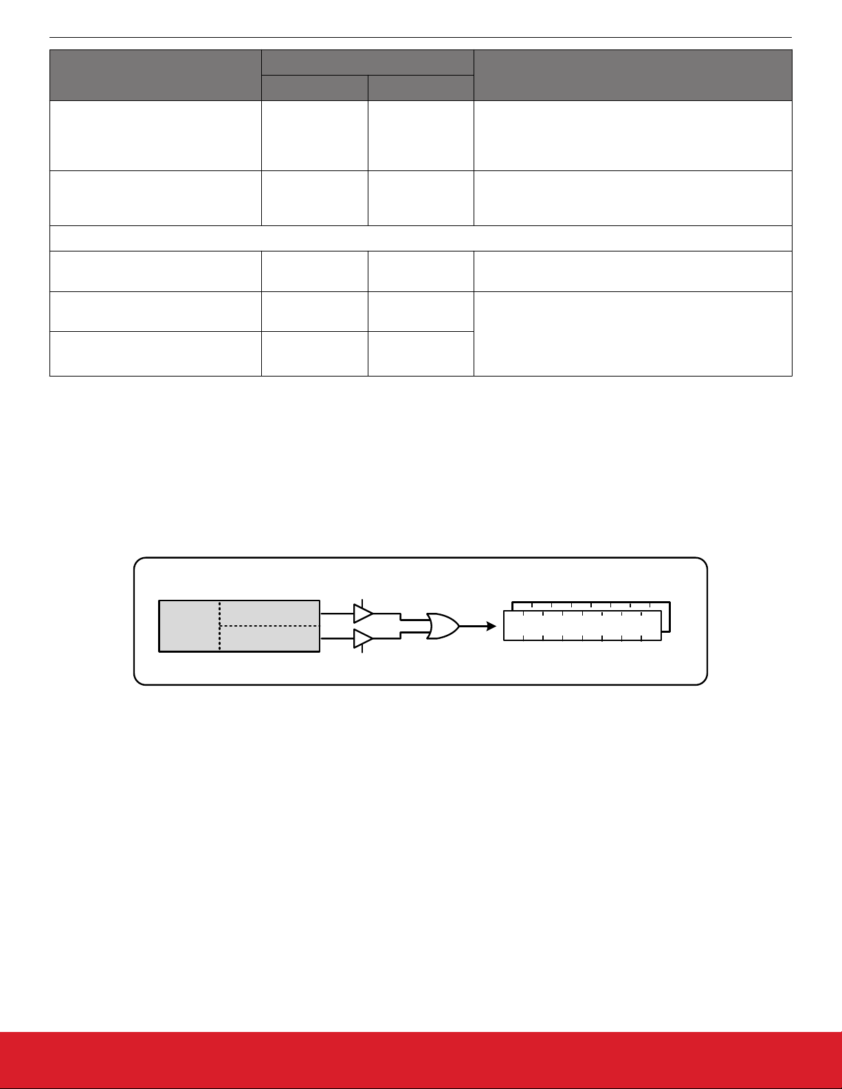
The final OOF status is determined by the combination of both a precise OOF monitor and a fast OOF monitor as shown in the figure
directly below. An option to disable either monitor is also available. The live OOF register always displays the current OOF state and its
sticky register bit stays asserted until cleared.
clock is monitored for frequency accuracy with respect to an OOF reference which it considers as its 0 ppm reference. This
Monitor
Precision
OOF
en
002E[7:0] -
0035[7:0]
0036[7:0] -
003D[7:0]
Sets the LOS trigger threshold and clear sensitivity for
IN3, IN2, IN1, IN0. These 16-bit values are determined
with the ClockBuilder Pro utility. The trigger threshold
sets the maximum period and the clear threshold sets
the minimum period.
Sticky
LOS
OOF
Fast
en
Live
Figure 5.9. OOF Status Indicator
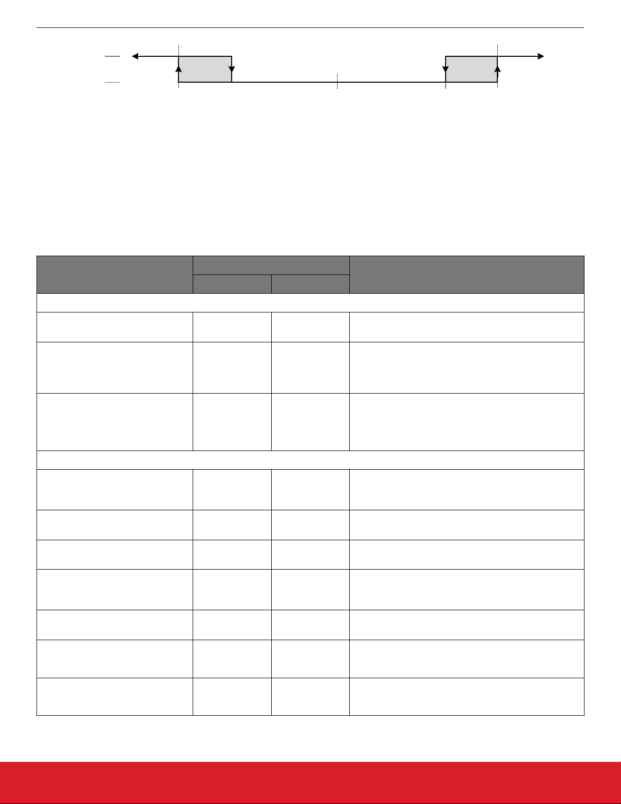
The Precision OOF monitor circuit measures the frequency of all input clocks to within up to ±0.0625 ppm accuracy with respect to the
selected OOF frequency reference. A valid input clock frequency is one that remains within the register-programmable OOF frequency
range of from ±0.0625 ppm to ±512 ppm in steps of 1/16 ppm. A configurable amount of hysteresis is also available to prevent the OOF
status from toggling at the failure boundary. An example is shown in the figure below. In this case, the OOF monitor is configured with a
valid frequency range of ±6 ppm and with 2 ppm of hysteresis. An option to use one of the input pins (IN0–IN3) as the 0 ppm OOF
reference instead of the XAXB pins is available. These options are all register configurable.
silabs.com | Building a more connected world. Rev. 0.9 | 31
Page 32
Si5397/96 Reference Manual
Clock Inputs
OOF Declared
f
IN
Hysteresis Hysteresis
OOF Cleared
-6 ppm
(Set)
-4 ppm
(Clear)
0 ppm
OOF
+4 ppm
(Clear)
+6 ppm
(Set)
Reference
Figure 5.10. Example of Precise OOF Monitor Assertion and De-assertion Triggers
The table
below lists the OOF monitoring and control registers. Because the precision OOF monitor needs to provide 1/16 ppm of frequency measurement accuracy, it must measure the monitored input clock frequencies over a relatively long period of time. This may
be too slow to detect an input clock that is quickly ramping in frequency. An additional level of OOF monitoring called the Fast OOF
monitor runs in parallel with the precision OOF monitors to quickly detect a ramping input frequency. The Fast OOF responds more
quickly and has larger thresholds.
Table 5.9. Out-of-Frequency Status Monitoring and Control Registers
Setting Name Hex Address [Bit Field] Function
Si5397 Si5396
OOF Status Indicators
OOF(3,2,1,0) 000D[7:4] 000D[7:4] OOF status monitor for IN3, IN2, IN1, IN0. Indicates if a
valid clock is detected or if a OOF condition is detected.
OOF(3,2,1,0)_FLG 0012[7:4] 0012[7:4] OOF status monitor sticky bits for IN3, IN2, IN1, IN0.
Sticky bits will remain asserted when an OOF event occurs until cleared. Writing a zero to a sticky bit will clear
it.
OOF(3,2,1,0)_INTR_MSK 0x0018[7:4] 0x0018[7:4] Marks OOF from generating INTRb interrupt for IN3-IN0.
0: Allow OOF interrupt (default)
1: Mask (ignore) OOF for interrupt
OOF Monitor Control and Settings
OOF_REF_SEL 0040[2:0] 0040[2:0] This selects the clock that the OOF monitors use as
their “0 ppm” reference. Selections are: XA/XB, IN0,
IN1, IN2, IN3.
OOF(3,2,1,0)_EN 003F[3:0] 003F[3:0] This allows to enable/disable the precision OOF monitor
for IN3, IN2, IN1, IN0.
FAST_OOF(3,2,1,0)_EN 003F[7:4] 003F[7:4] To enable/disable the fast OOF monitor for IN3, IN2,
IN1, IN0.
OOF(3,2,1,0)_SET_THR 0046[7:0] -
0049[7:0]
0046[7:0] -
0049[7:0]
Determines the OOF alarm set threshold for IN3, IN2,
IN1, IN0. Range is from ±2 ppm to ±500 ppm in steps of
2 ppm.
OOF(3,2,1,0)_CLR_THR 004A[7:0] -
004D[7:0]
004A[7:0] -
004D[7:0]
Determines the OOF alarm clear threshold for INx.
Range is from ±2 ppm to ±500 ppm in steps of 2 ppm.
FAST_OOF(3,2,1,0)_SET_THR 0x0051[7:0] -
0x0051[7:0] -
Determines the fast OOF alarm set threshold for IN3,
IN2, IN1, IN0.
0x0054[7:0]
FAST_OOF(3,2,1,0)_
0x0055 [7:0] -
CLR_THR
0x0058[7:0]
silabs.com | Building a more connected world. Rev. 0.9 | 32
0x0054[7:0]
0x0055 [7:0] -
0x0058[7:0]
Determines the fast OOF alarm clear threshold for IN3,
IN2, IN1, IN0.
Page 33
5.3.3 Loss of Lock (LOL) Fault Monitoring
Si5397/96 Reference Manual
Clock Inputs
There is
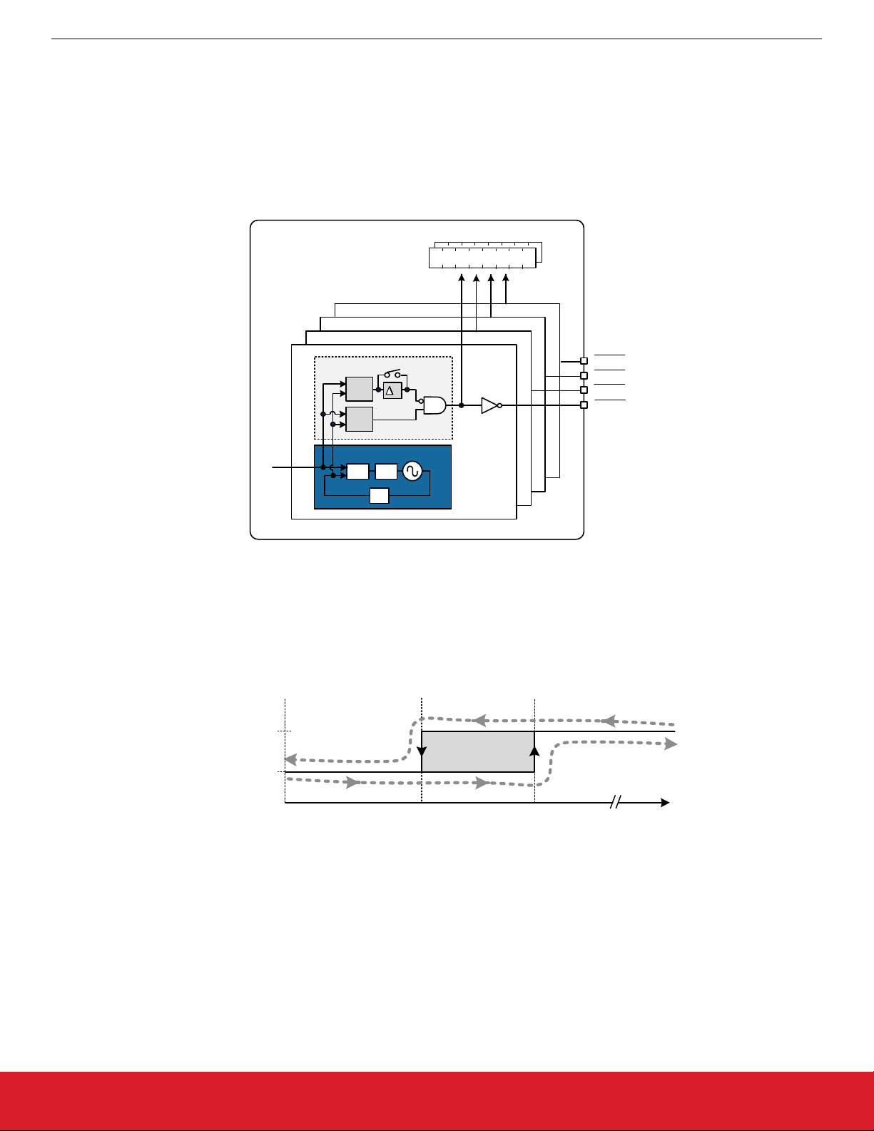
a loss of lock (LOL) monitor for each of the DSPLLs. The LOL monitor asserts a LOL register bit when a DSPLL has lost
synchronization with its selected input clock. There is also a dedicated loss of lock pin that reflects the loss of lock condition for each of
the DSPLLs (LOL_A, LOL_B, LOL_C, LOL_D). The LOL monitor functions by measuring the frequency difference between the input
and feedback clocks at the phase detector. There are two LOL frequency monitors, one that sets the LOL indicator (LOL Set) and another that clears the indicator (LOL Clear).
A block diagram of the LOL monitor is shown below. The live LOL register always displays the current LOL state and a sticky register
always stays asserted until cleared. The LOL pin reflects the current state of the LOL monitor.
Si5397
f
IN
LOL Monitor
LOL
Clear
LOL
Set
PD
LOL Status Registers
Live
DSPLL A
t
DSPLL A
LPF
÷M
Sticky
LOS
DSPLL D
DSPLL C
DSPLL B
LOL_D
LOL_C
LOL_B
LOL_A
Figure 5.11. LOL Status Indicators
The LOL frequency monitors have an adjustable sensitivity which is register configurable from 0.1 ppm to 10000 ppm. CBPro provides
a wide range of set and clear thresholds for the LOL function. Having two separate frequency monitors allows for hysteresis to help
prevent chattering of LOL status. An example configuration of the LOL set and clear thresholds is shown below.
Clear LOL
Threshold
Set LOL
Threshold
Lock Acquisition
LOL
LOCKED
Hysteresis
0
0.1 1
Lost Lock
10,000
Phase Detector Frequency Difference (ppm)
Figure 5.12. LOL Set and Clear Thresholds
An optional timer is available to delay clearing of the LOL indicator to allow additional time for the DSPLL to completely lock to the input
clock. The timer is also useful to prevent the LOL indicator from toggling or chattering as the DSPLL completes lock acquisition. The
configurable delay value depends on frequency configuration and loop bandwidth of the DSPLL and is automatically calculated using
the ClockBuilder Pro utility.
It is important to know that, in addition to being status bits, LOL optionally enables Fastlock.
silabs.com | Building a more connected world. Rev. 0.9 | 33
Page 34
Si5397/96 Reference Manual
Clock Inputs
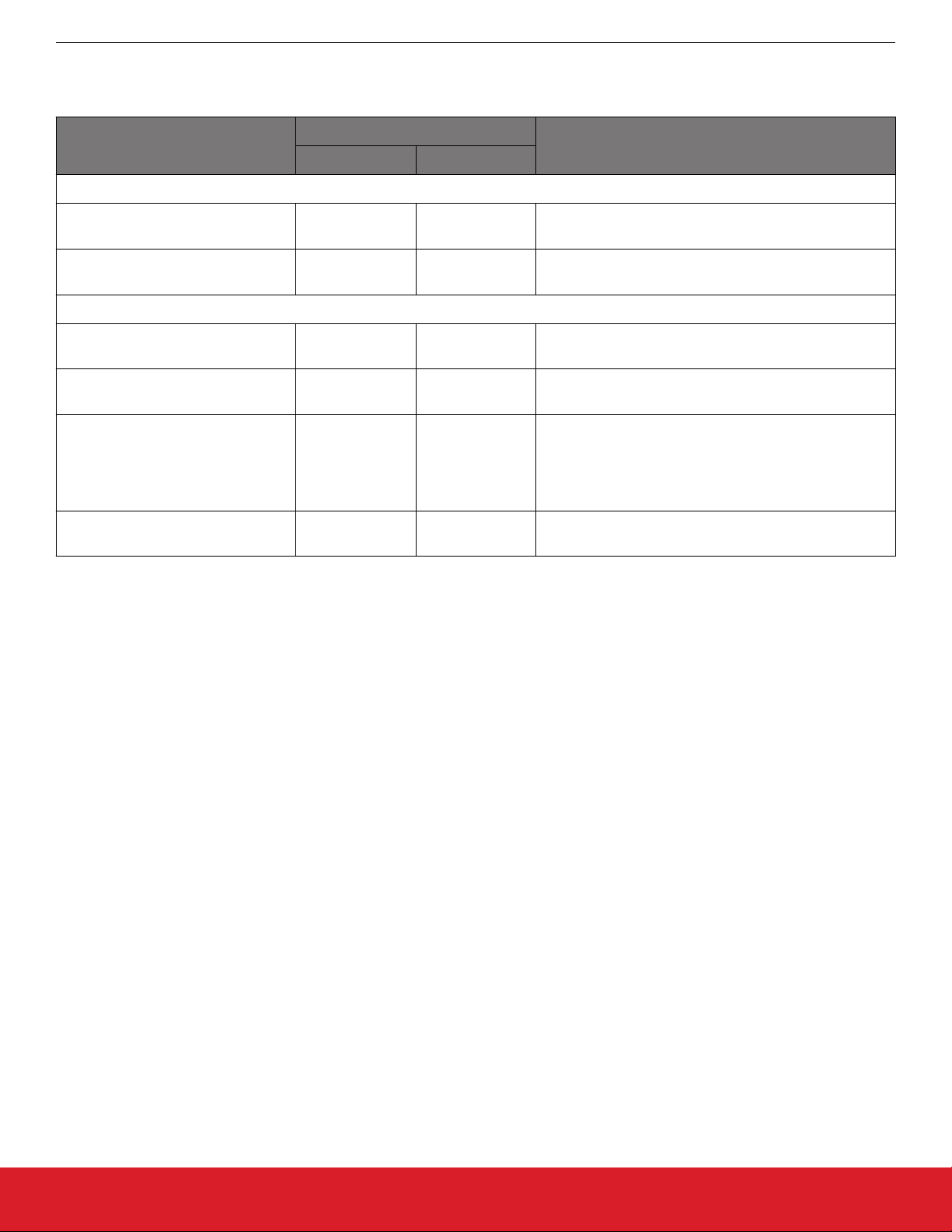
Table 5.10. Loss of Lock Status Monitor and Control Registers
Setting Name Hex Address [Bit Field] Function
Si5397 Si5396
LOL Status Indicators
LOL_PLL(D,C,B,A) 000E[3:0] 000E[1:0] Status bit that indicates if DSPLL A, B, C, or D is locked
to an input clock.
LOL_FLG_PLL(D,C,B,A) 0013[3:0] 0013[1:0] Sticky bits for LOL_[D,C,B,A]_STATUS register. Writing
a zero to a sticky bit will clear it.
LOL Fault Monitor Controls and Settings
LOL_SET_THR_PLL(D,C,B,A) 009E[7:0] -
009F[7:0]
LOL_CLR_THR_PLL(D,C,B,A) 00A0[7:0] -
00A1[7:0]
LOL_CLR_DELAY_DIV256_PLL(D,C,B,A)
00A4[7:0] -
00B6[7:0]
009E[7:0] Configures the loss of lock set thresholds for DSPLL A,
B, C, D.
00A0[7:0] Configures the loss of lock clear thresholds for DSPLL
A, B, C, D.
00A4[7:0] -
00AC[7:0]
This is a 29-bit register that configures the delay value
for the LOL Clear delay. Selectable from 4 ns to over
500 seconds. This value depends on the DSPLL frequency configuration and loop bandwidth. It is calculated using the ClockBuilder Pro utility
LOL_TIMER_EN_PLL(D,C,B,A) 00A2[3:0] 00A2[1:0] Allows bypassing the LOL Clear timer for DSPLL A, B,
C, D. 0- bypassed, 1-enabled
The settings in the table above are handled by ClockBuilder Pro. Manual settings should be avoided.
silabs.com | Building a more connected world. Rev. 0.9 | 34
Page 35
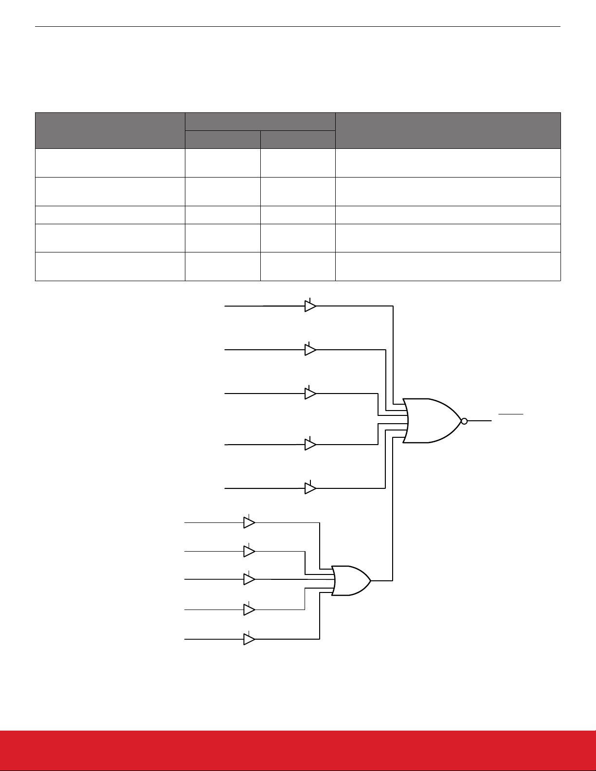
5.3.4 Interrupt Pin (INTR)
Si5397/96 Reference Manual
Clock Inputs
An interrupt
pin (INTR) indicates a change in state with any of the status indicators for any of the DSPLLs. All status indicators are
maskable to prevent assertion of the interrupt pin. The state of the INTR pin is reset by clearing the sticky status registers.
Table 5.11. Interrupt Mask Registers
Setting Name Hex Address [Bit Field] Function
Si5397 Si5396
LOS(3, 2, 1, 0)_INTR_MSK 0018[3:0] 0018[1:0] Prevents IN3, IN2, IN1, IN0 LOS from asserting the
INTR pin
OOF(3, 2, 1, 0)_INTR_MSK 0018[7:4] 0018[5:4] Prevents IN3, IN2, IN1, IN0 OOF from asserting the
INTR pin
LOSXAXB_INTR_MSK 0017[1] 0017[1] Prevents XAXB LOS from asserting the INTR pin
LOL_INTR_MSK_PLL(D,C,B,A) 0019[3:0] 0019[1:0] Prevents DSPLL D, C, B, A LOL from asserting the
INTR pin
HOLD_INTR_MSK_PLL(D,C,B,A) 0019[7:4] 0019[5:4] Prevents DSPLL D, C, B, A HOLD from asserting the
INTR pin
LOS[3-0]_INTR_MSK
LOS_FLG[3-0]
OOF[3-0]_INTR_MSK
OOF_FLG[3-0]
LOL_FLG_PLL[D:A]
HOLD_FLG_PLL[D:A]
CAL_FLG_PLL[D:A]
SYSINCAL_FLG
LOSXAXB_FLG
LOSREF_FLG
XAXB_ERR_FLG
SMBUS_TIMEOUT_FLG
LOL_INTR_MSK_PLL[D:A]
HOLD_INTR_MSK_PLL[D:A]
CAL_INTR_MSK_PLL[D:A]
SYSINCAL_INTR_MSK
LOSXAXB_INTR_MSK
LOSREF_INTR_MSK
XAXB_ERR_INTR_MSK
SMB_TMOUT_INTR_MSK
INTR
Figure 5.13. Interrupt Triggers and Masks
silabs.com | Building a more connected world. Rev. 0.9 | 35
Page 36

Si5397/96 Reference Manual
Clock Inputs
The _FLG bits are “sticky” versions of the alarm bits and will stay high until cleared. A _FLG bit can be cleared by writing a zero to the
_FLG bit. When a _FLG bit is high and its corresponding alarm bit is low, the _FLG bit can be cleared.
During run
time, the source of an interrupt can be determined by reading the _FLG register values and logically ANDing them with the
corresponding _MSK register bits (after inverting the _MSK bit values). If the result is a logic one, then the _FLG bit will cause an interrupt.
For example, if LOS_FLG[0] is high and LOS_INTR_MSK[0] is low, then the INTR pin will be active (low) and cause an interrupt. If
LOS[0] is zero and LOS_MSK[0] is one, writing a zero to LOS_MSK[0] will clear the interrupt (assuming that there are no other interrupt
sources). If LOS[0] is high, then LOS_FLG[0] and the interrupt cannot be cleared.
Note: The INTR pin may toggle during reset.
silabs.com | Building a more connected world. Rev. 0.9 | 36
Page 37

Si5397/96 Reference Manual
Outputs
6. Outputs
The Si5397 supports up to eight differential output drivers and the Si5396 supports four. Each driver has a configurable voltage amplitude and common mode voltage covering a wide variety of differential signal formats including LVPECL, LVDS, HCSL, with CML-compatible amplitudes. In addition to supporting differential signals, any of the outputs can be configured as dual single-ended LVCMOS
(3.3 V, 2.5 V, or 1.8 V) providing up to 16 single-ended outputs, or any combination of differential and single-ended outputs.
silabs.com | Building a more connected world. Rev. 0.9 | 37
Page 38
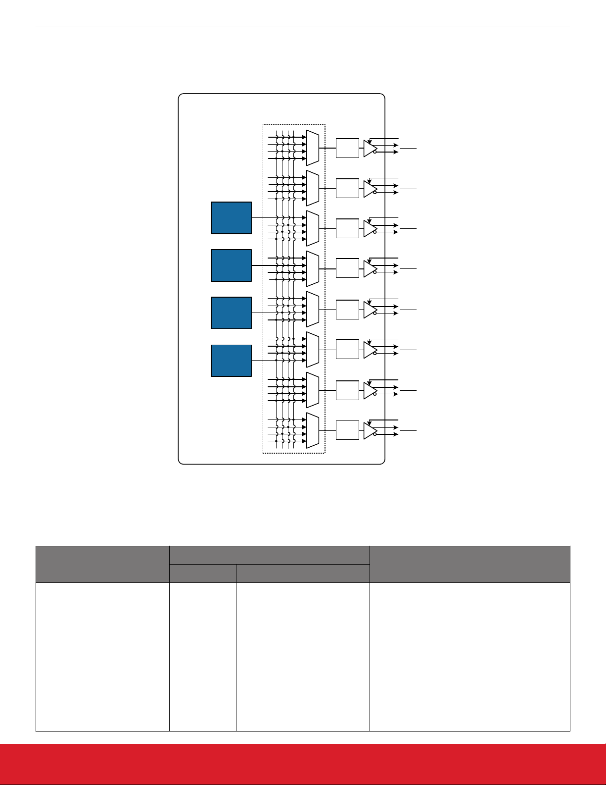
6.1 Output Crosspoint Switch
Si5397/96 Reference Manual
Outputs
A crosspoint
switch allows any of the output drivers to connect with any of the MultiSynths as shown in Figure 6.1 MultiSynth to Output
Driver Crosspoint on page 38. The crosspoint configuration is programmable and can be stored in NVM so that the desired output
configuration is ready at power up. Any MultiSynth output can connect to multiple output drivers.
Si5397
DSPLL
A
DSPLL
B
DSPLL
C
DSPLL
D
Output
Crosspoint
A
B
C
D
A
B
C
D
A
B
C
D
A
B
C
D
A
B
C
D
A
B
C
D
A
B
C
D
÷R
÷R
÷R
÷R
÷R
÷R
÷R
0
1
2
3
4
5
6
VDDO0
OUT0
OUT0
VDDO1
OUT1
OUT1
VDDO2
OUT2
OUT2
VDDO3
OUT3
OUT3
VDDO4
OUT4
OUT4
VDDO5
OUT5
OUT5
VDDO6
OUT6
OUT6
A
B
C
D
÷R
7
VDDO7
OUT7
OUT7
Figure 6.1. MultiSynth to Output Driver Crosspoint
The figure above is used to set up the routing from the MultiSynth frequency selection to the output.
Table 6.1. Output Driver Crosspoint Configuration Registers
Setting Name Hex Address [Bit Field] Function
Si5397A/B Si5397C/D Si5396
OUT0_MUX_SEL
010B[2:0]
010B[2:0]
0115[2:0]
Selects the DSPLL that each of the outputs are
connected to. Options are DSPLL_A, DSPLL_B,
OUT1_MUX_SEL
OUT2_MUX_SEL
OUT3_MUX_SEL
OUT4_MUX_SEL
OUT5_MUX_SEL
OUT6_MUX_SEL
0115[2:0]
011A[2:0]
011F[2:0]
0129[2:0]
012E[2:0]
0133[2:0]
011F[2:0]
0129[2:0]
012E[2:0]
—
—
—
011A[2:0]
0129[2:0]
012E[2:0]
—
—
—
DSPLL_C, or DSPLL_D.
OUT7_MUX_SEL
013D[2:0]
—
—
silabs.com | Building a more connected world. Rev. 0.9 | 38
Page 39
Si5397/96 Reference Manual
Outputs
6.2 Output Divider (R) Synchronization
output R dividers are reset to a known state during the power-up initialization period. This ensures consistent and repeatable
All the
phase alignment. Resetting the device using the RST pin or asserting the hard reset bit 0x001E[1] will give the same result. Soft reset
does not affect output alignment.
6.3 Performance Guidelines for Outputs
Whenever a number of high frequency, fast rise time, large amplitude signals are all close to one another there will be some amount of
crosstalk. The jitter generation of the Si5397/96 is so low that crosstalk can become a significant portion of the final measured output
jitter. Some of the crosstalk will come from the Si5397/96, and some will be introduced by the PCB. It is difficult (and possibly irrelevant)
to allocate the jitter portions between these two sources since the Si5397/96 must be attached to a board in order to measure jitter.
For extra fine tuning and optimization in addition to following the usual PCB layout guidelines, crosstalk can be minimized by modifying
the arrangements of different output clocks. For example, consider the following lineup of output clocks in following table.
Table 6.2. Example of Output Clock Placement
Output Not Recommended (Frequency MHz) Recommended (Frequency MHz)
0 155.52 155.52
1 156.25 155.52
2 155.52 622.08
3 156.25 Not used
4 622.08 Not used
5 625 156.25
6 Not used 156.25
7 Not used 625
Using this example, a few guidelines are illustrated:
1. Avoid adjacent
frequency values that are close. For example, a 155.52 MHz clock should not be placed next to a 156.25 MHz
clock. If the jitter integration bandwidth goes up to 20 MHz then keep adjacent frequencies at least 20 MHz apart.
2. Adjacent frequency values that are integer multiples of one another are allowed, and these outputs should be grouped together
when possible. Noting that because 155.52 MHz x 4 = 622.08 MHz, it is okay to place the pair of these frequency values close to
one another.
3. Unused outputs can be used to separate clock outputs that might otherwise interfere with one another.
If some outputs have tight jitter requirements while others are relatively loose, rearrange the clock outputs so that the critical outputs are
the least susceptible to crosstalk. These guidelines need to be followed by those applications that wish to achieve the highest possible
levels of jitter performance. Because CMOS outputs have large pk-pk swings, are single ended, and do not present a balanced load to
the VDDO supplies, they generate much more crosstalk than differential outputs. For this reason, CMOS outputs should be avoided in
jitter-sensitive applications. When CMOS clocks are unavoidable, even greater care must be taken with respect to the above guidelines.
For more information on these issues, see application note, "AN862: Optimizing Si534x Jitter Performance in Next Generation Internet
Infrastructure Systems.”
The ClockBuilder Pro Clock Placement Wizard is an easy way to reduce crosstalk for a given frequency plan. This feature can be accessed on the “Define Output Frequencies” page of ClockBuilder Pro in the lower left hand corner of the GUI. It is recommended to use
this tool after each project frequency plan change.
silabs.com | Building a more connected world. Rev. 0.9 | 39
Page 40
6.4 Output Signal Format
Si5397/96 Reference Manual
Outputs
The differential
output swing and common mode voltage are both fully programmable covering a wide variety of signal formats including
LVDS, LVPECL, and HCSL. For CML applications, see Section 6.4.9 Setting the Differential Output Driver to Non-Standard Amplitudes.
The differential formats can be either normal or low power. Low power format uses less power for the same amplitude but has the drawback of slower rise/fall times. The source impedance in low power format is much higher than 100 Ω. See Section 6.4.9 Setting the
Differential Output Driver to Non-Standard Amplitudes for register settings to implement variable amplitude differential outputs. In addi-
tion to supporting differential signals, any of the outputs can be configured as LVCMOS (3.3, 2.5, or 1.8 V) drivers providing up to 8 (for
the Si5396) single-ended outputs, or any combination of differential and single-ended outputs. Note also that CMOS output can create
much more crosstalk than differential outputs so extra care must be taken in their pin replacement so that other clocks that need the
lowest jitter are not on nearby pins. See AN862: Optimizing Jitter Performance in Next Generation Internet Infrastructure Systems for
additional information.
Table 6.3. Output Signal Format Control Registers
Setting Name Hex Address [Bit Field] Function
Si5397A/B Si5397C/D Si5396
OUT0_FORMAT
0109[2:0]
0109[2:0]
0113[2:0]
Selects the output signal format as differential or
LVCMOS.
OUT1_FORMAT
OUT2_FORMAT
OUT3_FORMAT
OUT4_FORMAT
OUT5_FORMAT
0113[2:0]
0118[2:0]
011D[2:0]
0127[2:0]
012C[2:0]
011D[2:0]
0127[2:0]
012C[2:0]
—
—
0118[2:0]
0127[2:0]
012C[2:0]
—
—
OUT6_FORMAT
OUT7_FORMAT
0131[2:0]
013B[2:0]
—
—
—
—
silabs.com | Building a more connected world. Rev. 0.9 | 40
Page 41
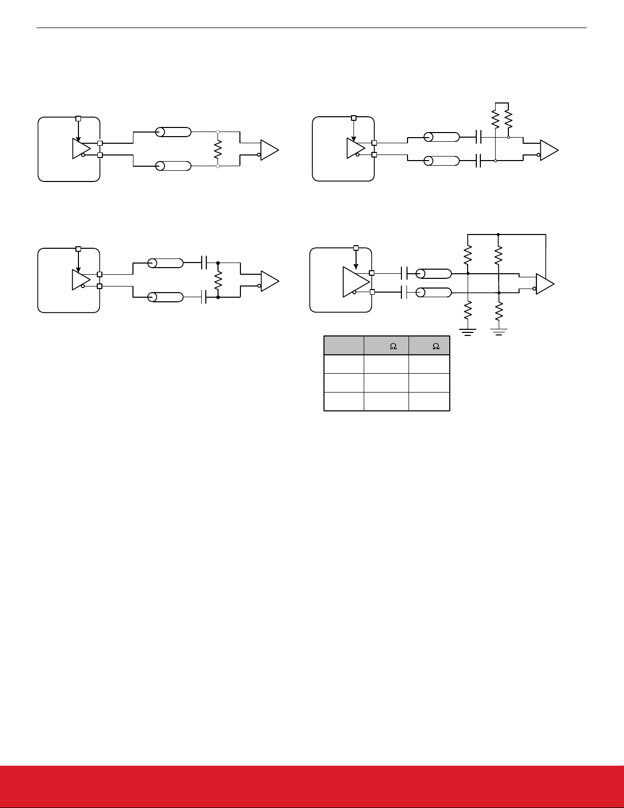
6.4.1 Differential Output Terminations
The differential output drivers support both ac and dc-coupled terminations as shown in the following figure.
AC Coupled CMLDC Coupled LVDS
LVDS: V
= 3.3V, 2.5V, 1.8V
DDO
OUTx
OUTxb
= 3.3V
DDO
, 2.5V
OUTx
OUTxb
50
50
V
50
100
50
Si5397/96 Reference Manual
Outputs
VDD – 1.3V
5050
0.1uF*
0.1uF*
AC Coupled LVDS/LVPECL
DDO
LVPECL: V
= 3.3V
DDO
LVDS: V
*All caps should have < 5 ohms capacitive reactance at the clock output frequency
, 1.8V
, 2.5V
= 3.3V, 2.5V
OUTx
OUTxb
0.1uF*
50
100
50
0.1uF*
Internally
self-biased
Figure 6.2. Supported Differential Output Terminations
= 3.3V, 2.5V. 1.8V
V
DDO
VDD
RX
3.3 V
2.5 V
1.8 V
OUTx
OUTxb
= 0.35 V
For V
CM
R1 R2
442
332
243
AC Coupled HCSL
0.1uF*
50
50
0.1uF*
56.2
59.0
63.4
VDD
RX
R1
R2
R1
Standard
HCSL
R2
Receiver
silabs.com | Building a more connected world. Rev. 0.9 | 41
Page 42
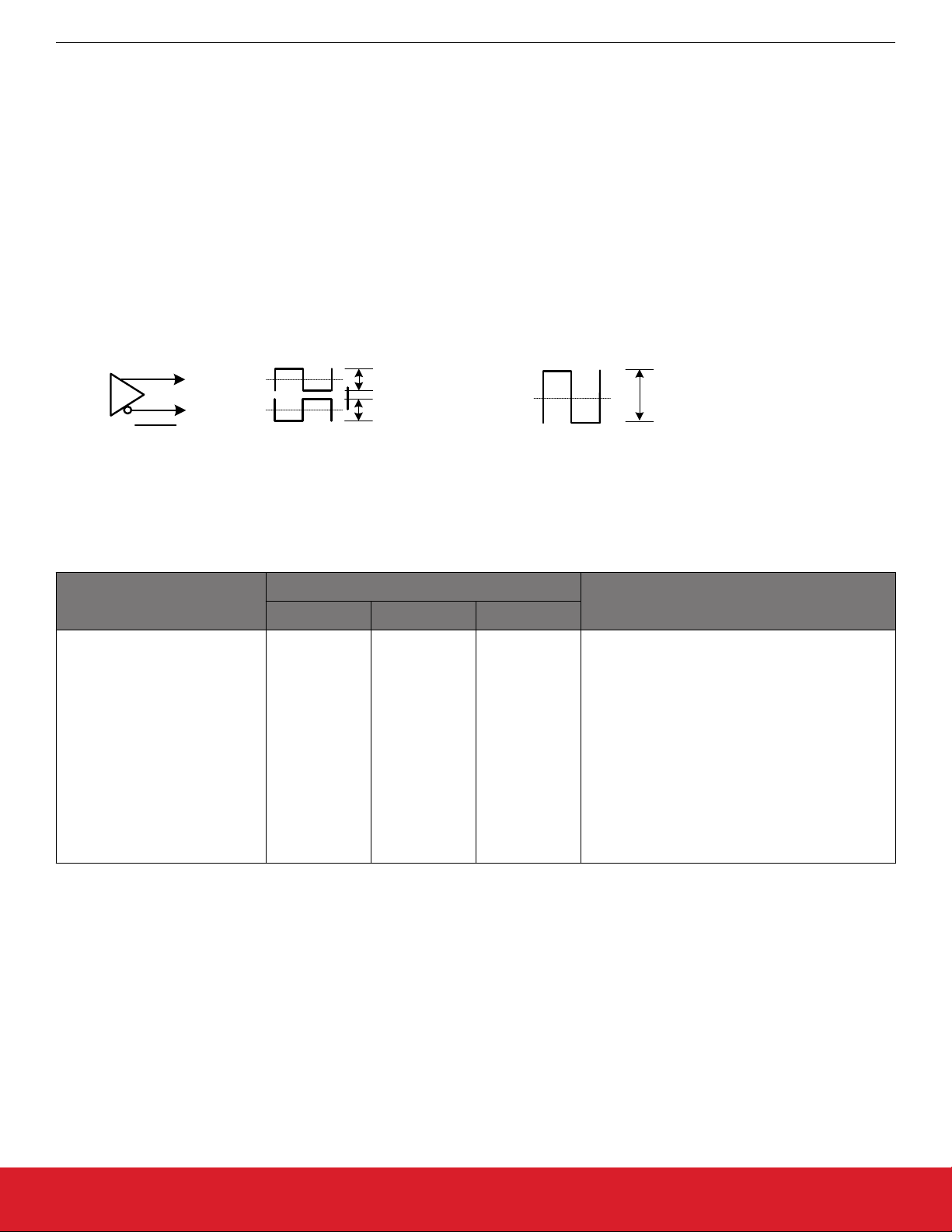
6.4.2 Differential Output Swing Modes
Si5397/96 Reference Manual
Outputs
There are
unique mode.
Differential Normal Swing Mode—This is the usual selection for differential outputs and should be used, unless there is a specific reason to do otherwise. When an output driver is configured in normal swing mode, its output swing is selectable as one of 7 settings
ranging from 200 mVpp_se to 800 mVpp_se in increments of 100 mV. Differential Output Voltage Swing Control Registers lists the
registers that control the output voltage swing. The output impedance in the Normal Swing Mode is 100 Ω differential. Any of the terminations shown in Figure 6.2 Supported Differential Output Terminations on page 41 are supported in this mode.
Differential High Swing Mode—When an output driver is configured in high swing mode, its output swing is configurable as one of 7
settings ranging from 400 mVpp_se to 1600 mVpp_se in increments of 200 mV. The output driver is in high impedance mode and supports standard 50 Ω PCB traces. Any of the terminations shown in Figure 6.2 Supported Differential Output Terminations on page 41
are supported. The use of High Swing mode will result in larger pk-pk output swings that draw less power. The trade off will be slower
rise and fall times.
Vpp_diff is 2 x Vpp_se as shown below.
two selectable differential output swing modes: Normal and High (also called low power mode). Each output can support a
OUTx
Vcm
Vcm
Vpp_se
Vpp_se
Vcm
Vpp_diff = 2*Vpp_se
OUTx
Figure 6.3. Vpp_se and Vpp_diff
Table 6.4. Differential Output Voltage Swing Control Registers
Setting Name Hex Address [Bit Field] Function
Si5397A/B Si5397C/D Si5396
OUT0_AMPL
OUT1_AMPL
OUT2_AMPL
OUT3_AMPL
OUT4_AMPL
OUT5_AMPL
OUT6_AMPL
OUT7_AMPL
010A[6:4]
0114[6:4]
0119[6:4]
011E[6:4]
0128[6:4]
012D[6:4]
0132[6:4]
013C[6:4]
010A[6:4]
011E[6:4]
0128[6:4]
012D[6:4]
—
—
—
—
0114[6:4]
0119[6:4]
0128[6:4]
012D[6:4]
—
—
—
—
Sets the differential voltage swing (amplitude) for
the output drivers in both normal and low-power
modes. See Table 6.10
LVPECL, and HCSL
mation.
Settings for LVDS,
on page 46 for more infor-
silabs.com | Building a more connected world. Rev. 0.9 | 42
Page 43
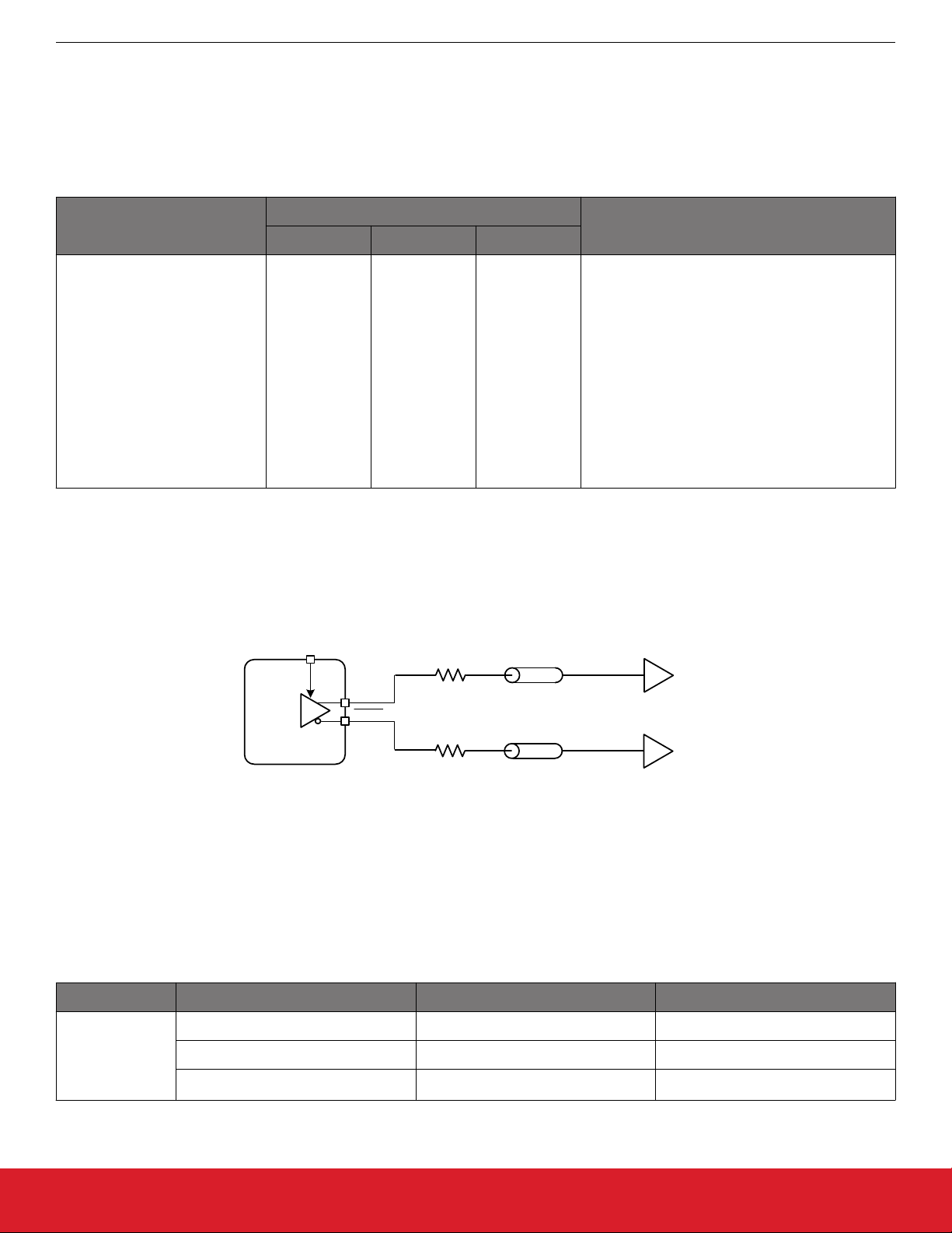
6.4.3 Programmable Common Mode Voltage for Differential Outputs
Si5397/96 Reference Manual
Outputs
The common
mode voltage (VCM) for the differential Normal and High Swing modes is programmable in 100 mV increments from 0.7
to 2.3 V depending on the voltage available at the output's VDDO pin. Setting the common mode voltage is useful when dc coupling the
output drivers. High swing mode may also cause an increase in the rise/fall time.
Table 6.5. Differential Output Common Mode Voltage Control Registers
Setting Name Hex Address [Bit Field] Function
Si5397A/B Si5397C/D Si5396
OUT0_CM
010A[3:0]
010A[3:0]
0114[3:0]
Sets the common mode voltage for the differential output driver. See Table 6.10 Settings for
OUT1_CM
OUT2_CM
OUT3_CM
OUT4_CM
OUT5_CM
OUT6_CM
OUT7_CM
0114[3:0]
0119[3:0]
011E[3:0]
0128[3:0]
012D[3:0]
0132[3:0]
013C[3:0]
011E[3:0]
0128[3:0]
012D[3:0]
—
—
—
—
0119[3:0]
0128[3:0]
012D[3:0]
—
—
—
—
LVDS, LVPECL, and HCSL
more information.
on page 46
for
6.4.4 LVCMOS Output Terminations
LVCMOS outputs are dc-coupled as shown in Figure 6.4 LVCMOS Output Terminations
on page 43.
DC Coupled LVCMOS
3.3V, 2.5V, 1.8V
= 3.3V, 2.5V
V
DDO
OUTx
OUTx
, 1.8V
50
Rs
50
Rs
Figure 6.4. LVCMOS Output Terminations
6.4.5 LVCMOS Output Impedance and Drive Strength Selection
Each
LVCMOS
driver has a configurable output impedance to accommodate different trace impedances and drive strengths. A source
termination resistor is recommended to help match the selected output impedance to the trace impedance. There are three programmable output impedance selections for each VDDO option as shown below. The value for the OUTx_CMOS_DRIVE bits are given.
Table 6.6. Output Impedance and Drive Strength Selections
VDDO OUTx_CMOS_DRV Source Impedance (Rs) Drive Strength (Iol/Ioh)
LVCMOS
0x01 38 Ω 10 mA
3.3 V
silabs.com | Building a more connected world. Rev. 0.9 | 43
0x02 30 Ω 12 mA
0x03
1
22 Ω 17 mA
Page 44
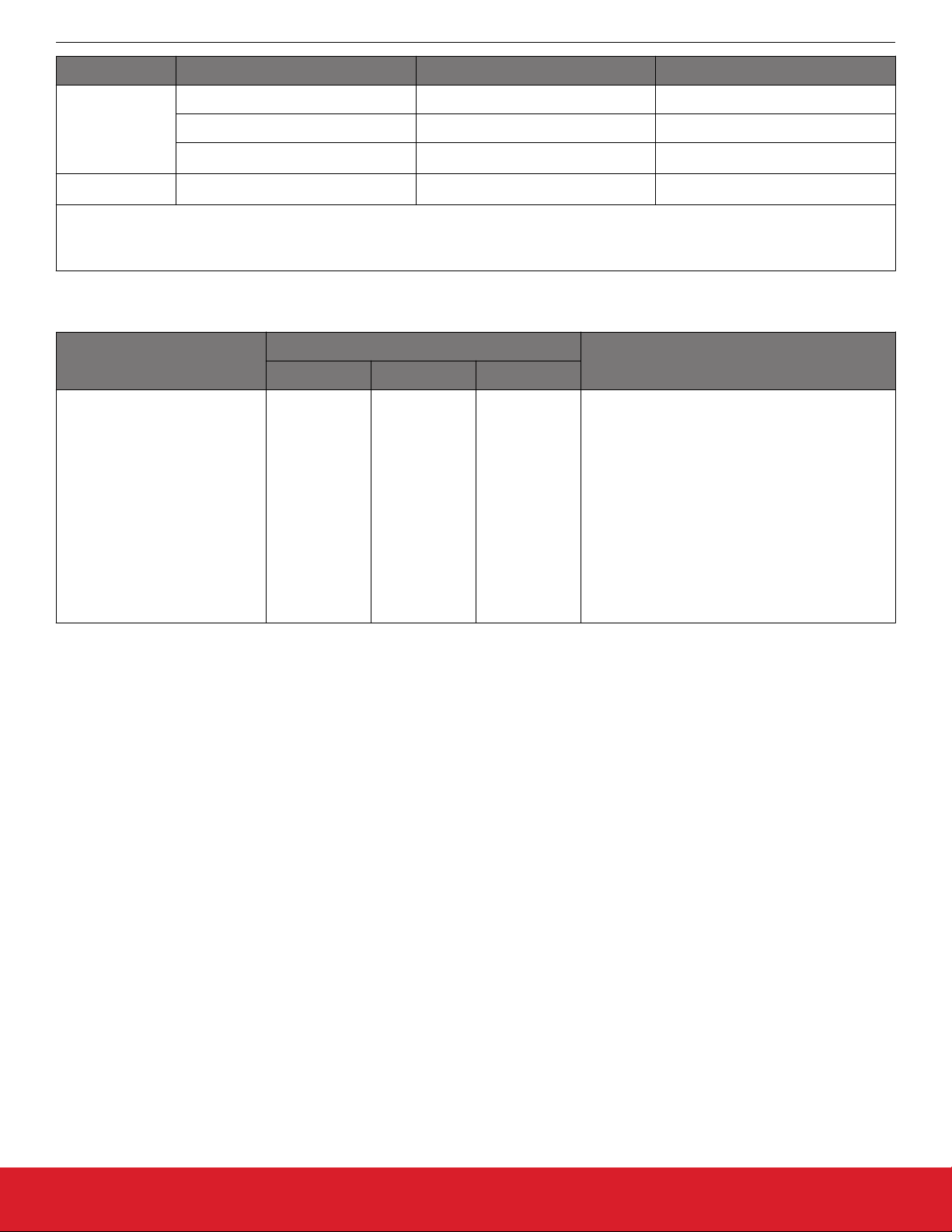
Si5397/96 Reference Manual
VDDO OUTx_CMOS_DRV Source Impedance (Rs) Drive Strength (Iol/Ioh)
0x01 43 Ω 6 mA
Outputs
2.5 V
1.8 V
0x02 35 Ω 8 mA
0x03
0x03
1
1
24 Ω 11 mA
31 Ω 5 mA
Note:
1.
Use of the lowest impedance setting is recommended for all supply voltages.
Table 6.7. LVCMOS Drive Strength Control Registers
Setting Name Hex Address [Bit Field] Function
Si5397A/B Si5397C/D Si5396
OUT0_CMOS_DRV
OUT1_CMOS_DRV
OUT2_CMOS_DRV
OUT3_CMOS_DRV
OUT4_CMOS_DRV
OUT5_CMOS_DRV
0109[7:6]
0113[7:6]
0118[7:6]
011D[7:6]
0127[7:6]
012C[7:6]
0109[7:6]
011D[7:6]
0127[7:6]
012C[7:6]
—
—
0118[7:6]
011D[7:6]
0127[7:6]
012C[7:6]
—
—
LVCMOS output impedance.
OUT6_CMOS_DRV
OUT7_CMOS_DRV
0131[7:6]
013B[7:6]
—
—
—
—
6.4.6 LVCMOS Output Signal Swing
The signal
swing (VOL/VOH) of the LVCMOS output drivers is set by the voltage on the VDDO pins. Each output driver has its own
VDDO pin allowing a unique output voltage swing for each of the LVCMOS drivers.
silabs.com | Building a more connected world. Rev. 0.9 | 44
Page 45
6.4.7 LVCMOS Output Polarity
Si5397/96 Reference Manual
Outputs
When a
driver is configured as an LVCMOS output it generates a clock signal on both pins (OUTx and OUTxb). By default the clock on
the OUTx pin is generated with the same polarity (in phase) with the clock on the OUTxb pin. The polarity of these clocks is configurable enabling complimentary clock generation and/or inverted polarity with respect to other output drivers.
Table 6.8. LVCMOS Output Polarity Control Registers
Setting Name Hex Address [Bit Field] Function
Si5397A/B Si5397C/D Si5396
OUT0_INV
010B[7:6]
010B[7:6]
0115[7:6]
Controls output polarity of the OUTx and OUTx pins when in
LVCMOS mode. Selections are:
OUT1_INV
OUT2_INV
0115[7:6]
011A[7:6]
011F[7:6]
0129[7:6]
011A[7:6]
0129[7:6]
OUTx_IN
OUTx OUTx Comment
V
OUT3_INV
OUT4_INV
OUT5_INV
OUT6_INV
OUT7_INV
011F[7:6]
0129[7:6]
012E[7:6]
0133[7:6]
013D[7:6]
012E[7:6]
—
—
—
—
012E[7:6]
—
—
—
—
Register
Settings
0 0 CLK CLK Both in phase (de-
fault)
0 1 CLK CLK OUTx inverted
1 0 CLK CLK OUTx and OUTx in-
verted
1 1 CLK CLK Both out of phase
OUTx_INV
Register Settings
00 CLK CLK Both in phase (default)
01 CLK CLKb OUTxb
10 CLKb CLK OUTx and OUTxb inverted
11 CLKb CLKb OUTx inverted
Table 6.9. Output Polarity of OUTx and OUTxb Pins in LVCMOS Mode
OUTx OUTxb Comment
silabs.com | Building a more connected world. Rev. 0.9 | 45
Page 46
Si5397/96 Reference Manual
Outputs
6.4.8 Output Driver Settings for LVPECL, LVDS, HCSL, and CML
Each differential output has four settings for control:
• Normal or Low Power Format
Amplitude (sometimes called Swing)
•
• Common Mode Voltage
• Stop High or Stop Low
The normal Format setting has a 100 Ω internal resistor between the plus and minus output pins. The Low Power Format setting removes this 100 Ω internal resistor and then the differential output resistance will be > 500 Ω. However as long as the termination impedance matches the differential impedance of the pcb traces the signal integrity across the termination impedance will be good. For the
same output amplitude the Low Power Format will use less power than the Normal Format. The Low Power Format also has a lower
rise/fall time than the Normal Format. See the Si5397/96 data sheet for the rise/fall time specifications. For LVPECL and LVDS standards, ClockBuilder Pro does not support the Low Power Differential Format. Stop High means that when the output driver is disabled
the plus output will be high and the minus output will be low. Stop Low means that when the output driver is disabled the plus output will
be low and the minus output will be high.
The Format, Amplitude and Common Mode settings for the various supported standards are shown in Table 6.10 Settings for LVDS,
LVPECL, and HCSL on page 46.
Table 6.10. Settings for LVDS, LVPECL, and HCSL
OUTx_FORMAT
1
Standard VDDO Volts OUTx_CM
(Decimal)
OUTx_AMPL
(Decimal)
001 = Normal Differential LVPECL 3.3 11 6
001 = Normal Differential LVPECL 2.5 11 6
002 = Low Power Differential LVPECL 3.3 11 3
002 = Low Power Differential LVPECL 2.5 11 3
001 = Normal Differential LVDS 3.3 3 3
001 = Normal Differential LVDS 2.5 11 3
001 = Normal Differential
Sub-LVDS
2
1.8 13 3
002 = Low Power Differential LVDS 3.3 3 1
002 = Low Power Differential LVDS 2.5 11 1
002 = Low Power Differential
002 = Low Power Differential
002 = Low Power Differential
002 = Low Power Differential
Sub-LVDS
HCSL
HCSL
HCSL
2
3
3
3
1.8 13 1
3.3 11 3
2.5 11 3
1.8 13 3
Note:
1.
The low-power format will cause the rise/fall time to increase by approximately a factor of two. See the Si5397/96
data sheet for
more information.
2. The common-mode voltage produced is not compliant with LVDS standards; therefore ac coupling the driver to an LVDS receiver
is highly recommended.
3. Creates HCSL compatible signal. See Section 5.3 Fault Monitoring.
The output differential driver can produce a wide range of output amplitudes that includes CML amplitudes. See Section 6.4.9 Setting
the Differential Output Driver to Non-Standard Amplitudes for additional information.
silabs.com | Building a more connected world. Rev. 0.9 | 46
Page 47
6.4.9 Setting the Differential Output Driver to Non-Standard Amplitudes
Si5397/96 Reference Manual
Outputs
In some
applications, it may be desirable to have larger or smaller differential amplitudes than those produced by the standard LVPECL
and LVDS settings, as selected by CBPro. In these cases, the following information describes how to implement these amplitudes by
writing to the OUTx_CM and OUTx_AMPL setting names. Contact Silicon Labs for assistance if you want your custom configured device to be programmed for any of the settings described here.
The differential output driver has a variable output amplitude capability and two basic formats, normal and low-power format. The difference between these two formats is that the normal format has an output impedance of ~100 Ω differential, and the low-power format
has an output impedance of > 500 Ω differential. Note that the rise/fall time is slower when using the Low Power Differential Format.
See the Si5397/96 data sheet for rise/fall time specifications.
If the standard LVDS or LVPECL compatible output amplitudes will not work for a particular application, the variable amplitude capability can be used to achieve higher or lower amplitudes. For example, a “CML” format is sometimes desired for an application. However,
CML is not a defined standard, and hence the amplitude of a CML signal for one receiver may be different than that of another receiver.
When the output amplitude needs to be different than standard LVDS or LVPECL, the Common Mode Voltage settings must be set as
shown in Table 6.11 Output Differential Common Mode Voltage Settings on page 47. No settings other than these are supported as
the signal integrity could be compromised. In addition, the output driver should be ac-coupled to the load so that the common-mode
voltage of the driver is not affected by the load.
Table 6.11. Output Differential Common Mode Voltage Settings
VDDOx (Volts) Differential
Format
OUTx_FORMAT Common
Mode Voltage (Volts)
OUTx_CM
3.3 Normal 0x1 2.0 0xB
3.3 Low Power 0x2 1.6 0x7
2.5 Normal 0x1 1.3 0xC
2.5 Low Power 0x2 1.1 0xA
1.8 Normal 0x1 0.8 0xD
1.8 Low Power 0x2 0.8 0xD
The differential amplitude can be set as shown in the following table.
Table 6.12. Typical Differential Amplitudes
OUTx_AMPL Normal Differential Format
(Vpp SE mV – Typical)
0 130 200
1 230 400
2 350 620
3 450 820
4 575 1010
5 700 1200
6 810
7 920
1
Low-Power Differential Format
(Vpp SE mV – Typical)
2
1350
2
1600
Note:
1.
These amplitudes are based upon a 100
Ω differential termination.
2. In low-power mode and VDDOx = 1.8 V, OUTx_AMPL may not be set to 6 or 7.
silabs.com | Building a more connected world. Rev. 0.9 | 47
Page 48
Si5397/96 Reference Manual
Outputs
Note: High-Speed Differential
Mode in ClockBuilder Pro output setting page sets OUTx_AMP to 7 in order to compensate for channel
loss at high frequency.
See the register map portion of this document for additional information about OUTx_FORMAT, OUTx_CM and OUTx_AMPL. Contact
Silicon Labs for assistance if you require a factory-programmed device to be configured for any of the output driver settings listed
above.
6.5 Output Enable/Disable
The OEb pin provides a convenient method of disabling or enabling the output drivers. When the OEb pin is held high all outputs will be
disabled. When the pin is not driven, the device defaults to all outputs on. Outputs in the enabled state can be individually disabled
through register control. If the pin is high register control is disabled and all outputs will be disabled.
Table 6.13. Output Enable/Disable Control Registers
Setting Name Hex Address [Bit Field] Function
Si5397A/B Si5397C/D Si5396
OUTALL_DISABLE_
LOW
0102[0] 0102[0] 0102[0] Allows disabling all output drivers: 0 - all outputs
disabled, 1 - all outputs controlled by the
OUTx_OE bits. Note that if the OE pin is held
high (disabled), then all assigned outputs will be
disabled regardless of the state of this register
bit.
OUT0_OE
OUT1_OE
OUT2_OE
OUT3_OE
OUT4_OE
OUT5_OE
OUT6_OE
OUT7_OE
OUT_DIS_MSK_LOL_
PLL(D,C,B,A)
OUT_DIS_MSK_
LOSXAXB
OUT0_DIS_STATE
OUT1_DIS_STATE
0108[1]
0108[1]
0012[1]
Allows enabling/disabling individual output drivers. Note that the OE pin must be held low in or-
0112[1]
0117[1]
011C[1]
0126[1]
012B[1]
0130[1]
013A[1]
011C[1]
0126[1]
012B[1]
—
—
—
—
0117[1]
0126[1]
012B[1]
—
—
—
—
der to enable an output with these register bits.
0142[3:0] 0142[3:0] 0142[1:0] Determines if the outputs are disabled during an
LOL condition. 0 = outputs disable on LOL, 1 =
outputs remain enabled during LOL (default).
This option is independently configured for each
DSPLL. See DRVx_DIS_SRC registers.
0141[6] 0141[6] 0141[6] Determines if outputs are disabled during an
LOSXAXB condition. 0 = all outputs disabled on
LOSXAXB (default), 1 = outputs remain enabled
during LOSXAXB condition.
0109[5:4]
0109[5:4]
0113[5:4]
Sets the state for the outputs when they are disabled.
0113[5:4]
011D[5:4]
0118[5:4]
OUT2_DIS_STATE
OUT3_DIS_STATE
OUT4_DIS_STATE
OUT5_DIS_STATE
OUT6_DIS_STATE
OUT7_DIS_STATE
silabs.com | Building a more connected world. Rev. 0.9 | 48
0118[5:4]
011D[5:4]
0127[5:4]
012C[5:4]
0131[5:4]
013B[5:4]
0127[5:4]
012C[5:4]
—
—
—
—
0127[5:4]
012C[5:4]
—
—
—
—
Page 49
6.5.1 Output Driver State When Disabled
Si5397/96 Reference Manual
Outputs
The disabled
state of an output driver is configurable as disable low or disable high. When the output driver is disabled, the outputs will
drive either logic high or logic low, selectable by the user. The output common mode voltage is maintained while the driver is disabled,
reducing enable/disable transients. By contrast, powering down the driver rather than disabling it increases output impedance and shuts
off the output common mode voltage. For all output drivers connected in the system, it is recommended to use Disable rather than
Powerdown to reduce enable/disable common mode transients. Unused outputs may be left unconnected, powered down to reduce
current draw, and, with the corresponding VDDOx, left unconnected.
Table 6.14. Output Driver State Control Registers
Setting Name Hex Address [Bit Field] Function
Si5397A/B Si5397C/D Si5396
OUTALL_DISABLE_
LOW
0102[0] 0102[0] 0102[0] Allows disabling all output drivers: 0 - all outputs
disabled, 1 - all outputs controlled by the
OUTx_OE bits. Note that if the OE pin is held
high (disabled), then all assigned outputs will be
disabled regardless of the state of this register
bit.
OUT0_OE
0108[1]
0108[1]
0012[1]
Allows enabling/disabling individual output drivers. Note that the OE pin must be held low in or-
OUT1_OE
OUT2_OE
OUT3_OE
0112[1]
0117[1]
011C[1]
011C[1]
0126[1]
012B[1]
0117[1]
0126[1]
012B[1]
der to enable an output with these register bits.
OUT4_OE
OUT5_OE
OUT6_OE
OUT7_OE
OUT_DIS_MSK_LOL_
PLL(D,C,B,A)
OUT_DIS_MSK_
LOSXAXB
OUT0_DIS_STATE
OUT1_DIS_STATE
OUT2_DIS_STATE
OUT3_DIS_STATE
OUT4_DIS_STATE
OUT5_DIS_STATE
0126[1]
012B[1]
0130[1]
013A[1]
—
—
—
—
—
—
—
—
0142[3:0] 0142[3:0] 0142[1:0] Determines if the outputs are disabled during an
LOL condition. 0 = outputs disable on LOL, 1 =
outputs remain enabled during LOL (default).
This option is independently configured for each
DSPLL. See DRVx_DIS_SRC registers.
0141[6] 0141[6] 0141[6] Determines if outputs are disabled during an
LOSXAXB condition. 0 = all outputs disabled on
LOSXAXB (default), 1 = outputs remain enabled
during LOSXAXB condition.
0109[5:4]
0109[5:4]
0113[5:4]
Sets the state for the outputs when they are disabled.
0113[5:4]
0118[5:4]
011D[5:4]
0127[5:4]
012C[5:4]
011D[5:4]
0127[5:4]
012C[5:4]
—
—
0118[5:4]
0127[5:4]
012C[5:4]
—
—
OUT6_DIS_STATE
OUT7_DIS_STATE
silabs.com | Building a more connected world. Rev. 0.9 | 49
0131[5:4]
013B[5:4]
—
—
—
—
Page 50
6.5.2 Synchronous Output Enable/Disable Feature
Si5397/96 Reference Manual
Outputs
The output
drivers provide a selectable synchronous enable/disable feature when OUTx_SYNC_EN = 1. Output drivers with this feature
turned on will wait until a clock period has completed before the driver is disabled or enabled. This prevents unwanted runt pulses from
occurring when disabling an output. When this feature is turned off OUTx_SYNC_EN = 0, the output clock will disable immediately without waiting for the period to complete and will enable immediately without waiting a period to complete. The default state is for the synchronous output disable/enable to be turned on OUTx_SYNC_EN = 1 .
Table 6.15. Synchronous Disable Control Registers
Setting Name Hex Address [Bit Field] Function
Si5397A/B Si5397C/D Si5396
OUT0_SYNC_EN
0109[3]
0109[3]
0113[3]
Selects Synchronous or Asynchronous output
disable. 1= synchronous, 0 = asynchronous. De-
OUT1_SYNC_EN
OUT2_SYNC_EN
OUT3_SYNC_EN
OUT4_SYNC_EN
OUT5_SYNC_EN
OUT6_SYNC_EN
OUT7_SYNC_EN
0113[3]
0118[3]
011D[3]
0127[3]
012C[3]
0131[3]
013B[3]
011D[3]
0127[3]
012C[3]
—
—
—
—
0118[3]
0127[3]
012C[3]
—
—
—
—
fault is synchronous mode.
6.6 Output Buffer Supply Voltage Selection
These power supply settings must match the actual VDDOx voltage so that the output driver operates properly.
Table 6.16. OUTx VDD Settings
Setting Name Description
OUTx_VDD_SEL_EN These bits are set to 1 and should not be changed
OUTx_VDD_SEL These bits are set by CBPro to match the expected VDDOx voltage. 0: 3.3 V; 1:
1.8 V; 2: 2.5 V; 3: Reserved
silabs.com | Building a more connected world. Rev. 0.9 | 50
Page 51
Si5397/96 Reference Manual
Digitally-Controlled Oscillator (DCO) Mode
7. Digitally-Controlled Oscillator (DCO) Mode
The DSPLLs support a DCO mode where their output frequencies are adjustable in pre-defined steps given by frequency step words
(FSTEPW). The frequency adjustments are controlled through the serial interface or by pin control using frequency increments (FINC)
or decrements (FDEC). A FINC will add the frequency step word to the DSPLL output frequency, while a FDEC will decrement it. The
DCO mode is available when the DSPLL is operating in locked mode. Note that the maximum FINC/FDEC update rate, by either hardware or software, is 1 MHz. Each DSPLL being used in DCO mode should have fractional M division enabled by setting the appropriate
M_FRAC_EN_PLLx = 0x3B for proper operation.
Note: DCO mode is not available when in free run or when in holdover. A large freq step can assert LOL on the relevant DSPLL. The
step sizes and frequency of operation need to be considered with the LOL settings and BW.
Table 7.1. Fractional M Divider Enable Controls
Setting Name Hex Address [Bit Field] Function
Si5397 Si5396
M_FRAC_EN_PLLA 0x0421[5:0] 0x0421[5:0] DSPLL feedback M divider fractional enable.
M_FRAC_EN_PLLB 0x0521[5:0] 0x0521[5:0]
M_FRAC_EN_PLLC 0x0621[5:0] —
M_FRAC_EN_PLLD 0x0721[5:0] —
0x2B: Integer-only division
0x3B Fractional (or Integer) division
Required for DCO operation.
silabs.com | Building a more connected world. Rev. 0.9 | 51
Page 52
7.1 Frequency Increment/Decrement Using Pin Controls
Si5397/96 Reference Manual
Digitally-Controlled Oscillator (DCO) Mode
Controlling the
output frequency with pin controls is available on the Si5397. This feature involves asserting the FINC or FDEC pins to
increment or decrement the DSPLL frequency. The DSPLL_SEL pins select which DSPLL output frequency is affected by the frequency change. The DSPLL_SEL pin selection is in the table below and follows the same logic as the register control settings for
FSTEP_PLL, register 0x0020[3:2].The frequency step words (FSTEPW) define the amount of frequency change for each FINC or
FDEC. The FSTEPW may be written once or may be changed after every FINC/FDEC assertion. Note that the DSPLL_SEL pins are
not available on the Si5346. Both the FINC and FDEC inputs are rising-edge-triggered and must meet the data sheet minimum pulse
width (PW) specifications.
Note: When the FINC/FDEC pins on the Si5397 are unused, the FDEC pin must be pulled down with an external pull-down resistor or
jumper. The FINC pin has an internal pull-down and may be left unconnected when not in use.
Table 7.2. 0x0020 DSPLL_SEL[1:0] Control of FINC/FDEC for DCO
Reg Address Bit Field Type Name Description
0x0020 0 R/W FSTEP_PLL_SIN-
0: DSPLL_SEL[1:0] pins and bits are disabled.
GLE
1: DSPLL_SEL[1:0] pins or FSTEP_PLL bits are enabled. See FSTEP_PLL_REGCTRL
0x0020 1 R/W FSTEP_PLL_REGC
Only functions when FSTEP_PLL_SINGLE = 1.
TRL
0: DSPLL_SELx pins are enabled, and the corresponding register bits are disabled.
1: DSPLL_SELx_REG register bits are enabled, and
the corresponding pins are disabled.
0x0020 3:2 R/W FSTEP_PLL[1:0]
(reg)
DSPLL_SEL[1:0]
(pin)
Register version of the DSPLL_SEL[1:0] pins. Used to
select which PLL (M divider) is affected by FINC/FDEC.
0: DSPLL A M-divider
1: DSPLL B M-divider
2: DSPLL C M-divider
3: DSPLL D M-divider
silabs.com | Building a more connected world. Rev. 0.9 | 52
Page 53
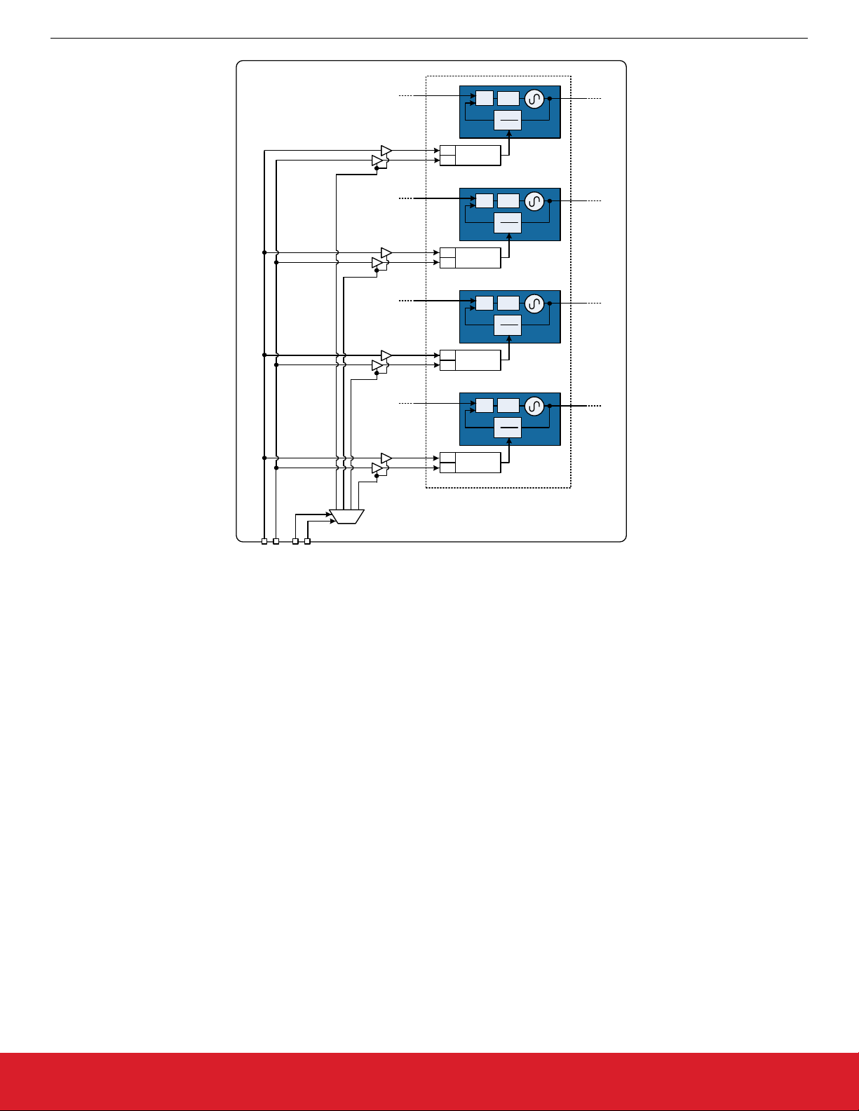
Si5397
PD
Frequency
+
Step Word
-
0x0423 – 0x0429
PD
Frequency
+
Step Word
-
0x0523 – 0x0529
PD
Frequency
+
Step Word
-
0x0623 – 0x0629
PD
Frequency
+
Step Word
-
0x0724 – 0x072A
Si5397/96 Reference Manual
Digitally-Controlled Oscillator (DCO) Mode
LPF
M
n_A
÷
M
A
d_
DSPLL A
LPF
M
n_B
÷
M
B
d_
DSPLL B
LPF
M
n_C
÷
M
C
d_
DSPLL C
LPF
M
n_D
÷
M
D
d_
DSPLL D
FINC
FDEC
DSPLL_SEL0
DSPLL_SEL1
Figure 7.1. Controlling the DCO Mode By Pin Control
silabs.com | Building a more connected world. Rev. 0.9 | 53
Page 54
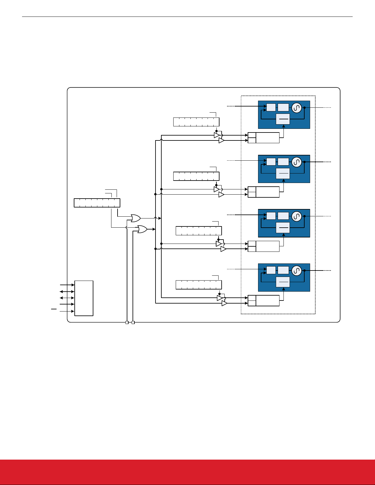
7.2 Frequency Increment/Decrement Using the Serial Interface
Si5397/96 Reference Manual
Digitally-Controlled Oscillator (DCO) Mode
Controlling the
DSPLL frequency through the serial interface is available on both the Si5397 and Si5396. This can be performed by
asserting the FINC or FDEC bits to activate the frequency change defined by the frequency step word. A set of mask bits selects the
DSPLL(s) that is affect by the frequency change. The FINC and FDEC pins can also be used to trigger a frequency change. Note that
both the FINC and FDEC register bits are rising-edge-triggered and self-clearing.
Each DSPLL being used in DCO mode should have fractional M division enabled by setting the appropriate M_FRAC_EN_PLLx=0x3B
for proper operation. See AN909: DCO Application with the Jitter Attenuators for related information.
Si5397
PD
PD
LPF
M
n_A
÷
M
d_
A
DSPLL A
LPF
M
n_B
÷
M
B
d_
DSPLL B
FINC
FDEC
0x001D
FSW_MASK_A
0x0422
FSW_MASK_B
0x0522
Frequency
+
Step Word
-
0x0423 – 0x0429
Frequency
+
Step Word
-
0x0523 – 0x0529
I2C_SEL
SDA/SDIO
A1/SDO
SCLK
A0/CS
SPI/
2
I
C
FSW_MASK_C
0x0622
Frequency
+
Step Word
-
0x0623 – 0x0629
FSW_MASK_D
0x0723
Frequency
+
Step Word
-
0x0724 – 0x072A
FINC
FDEC
Figure 7.2. Controlling the DCO Mode Using the Serial Interface
PD
PD
LPF
M
n_C
÷
M
d_
C
DSPLL C
LPF
M
n_D
÷
M
d_
D
DSPLL D
silabs.com | Building a more connected world. Rev. 0.9 | 54
Page 55
Si5397/96 Reference Manual
Digitally-Controlled Oscillator (DCO) Mode
Table 7.3. Frequency Increment/Decrement Control Registers
Setting Name Hex Address [Bit Field] Function
Si5397 Si5396
FINC 001D[0] 001D[0] Asserting this bit will increase the DSPLL output fre-
quency by the frequency step word.
FDEC 001D[1] 001D[1] Asserting this bit will decrease the DSPLL output fre-
quency by the frequency step word.
M_FSTEPW_PLLA 0423[7:0] -
0429[7:0]
M_FSTEPW_PLLB 0523[7:0] -
0529[7:0]
M_FSTEPW_PLLC 0623[7:0] -
0423[7:0] -
0429[7:0]
0523[7:0] -
0529[7:0]
—
This is a 56-bit frequency step word for DSPLL A, B, C,
D. The FSTEPW will be added or subtracted to the
DSPLL output frequency during assertion of the FINC/
FDEC bits or pins. The FSTEPW is calculated based on
the frequency configuration and is easily calculated using ClockBuilder Pro utility.
0629[7:0]
M_FSTEPW_PLLD 0724[7:0] -
—
072A[7:0]
M_FSTEP_MSK_PLLA 0422[0] 0422[0] This mask bit determines if a FINC or FDEC affects
M_FSTEP_MSK_PLLB 0522[0] 0522[0]
M_FSTEP_MSK_PLLC 0622[0] —
DSPLL A, B, C, D. 0 = FINC/FDEC will increment/decrement the FSTEPW to the DSPLL. 1 = Ignores FINC/
FDEC.
M_FSTEP_MSK_PLLD 0723[0] —
M_FRAC_EN_PLLA 0x0421[5:0] 0x0421[5:0] DSPLL feedback M divider fractional enable.
M_FRAC_EN_PLLB 0x0521[5:0] 0x0521[5:0] 0x2B: Integer-only division
M_FRAC_EN_PLLC 0x0621[5:0] — 0x3B: Fractional (or Integer) division
M_FRAC_EN_PLLD 0x0721[5:0] — Required for DCO operation.
silabs.com | Building a more connected world. Rev. 0.9 | 55
Page 56
Si5397/96 Reference Manual
Digitally-Controlled Oscillator (DCO) Mode
7.2.1 DCO with Direct Register Writes
In addition to the register-based FINC/FDEC described above, updated values for the DSPLL feedback M divider value may be updated
directly by
merator value will take effect and the output frequency will change without any glitches. The M divider numerator and denominator
terms (Mx_NUM and Mx_DEN) can be left and right-shifted so that the least significant bit of the numerator word represents the exact
step resolution that is needed for your application. Each individual M divider has its own update bit (Mx_UPDATE) that must be written
to cause the new numerator value to take effect. All M dividers can be updated at the same time by issuing a Soft Reset.
Changing the DSPLL feedback M divider value while the device is operating will not generate any glitches on affected outputs. The
frequency settling to the new value will be determined by the Loop BW of the DSPLL. All other outputs generated by other DSPLLs will
be unaffected by this update. It is generally recommended to avoid dynamically changing the M divider denominator (Mx_DEN) as, in
some cases, a small output phase shift may be observed when the update becomes active. However, by using the proper combination
of settings for the particular frequency plan, it is possible to avoid this entirely. If your application requires dynamic changes to an M
divider denominator, contact Silicon Labs at https://www.silabs.com/support/pages/contacttechnicalsupport.aspx.
Setting Name Hex Address [Bit Field] Function
M_NUM_PLLA 0x0415–0x041B 0x0415–0x041B 56-bit DSPLL feedback M divider Numerator.
M_NUM_PLLB 0x0515–0x051B 0x0515–0x051B
the user. When the M divider numerator (Mx_NUM) and its corresponding update bit (Mx_UPDATE) is written, the new nu-
Table 7.4. Direct DCO Control Registers
Si5397 Si5396
M_NUM_PLLC 0x0615–0x061B —
M_NUM_PLLD 0x0716–0x071C —
M_DEN_PLLA 0x041C–0x041F 0x041C–0x041F 32-bit DSPLL feedback M divider Denominator.
M_DEN_PLLB 0x051C–0x051F 0x051C–0x051F
M_DEN_PLLC 0x061C–0x061F —
M_DEN_PLLD 0x071D–0x0720 —
M_UPDATE_PLLA 0x0420[0] 0x0420[0] Must write a 1 to this bit to cause the individual M divider
M_UPDATE_PLLB 0x0520[0] 0x0520[0]
M_UPDATE_PLLC 0x0620[0] —
changes to take effect. Note that a corresponding
SOFT_RST_PLLx or device SOFT_RST will also update
the M divider values.
M_UPDATE_PLLD 0x0721[0] —
silabs.com | Building a more connected world. Rev. 0.9 | 56
Page 57
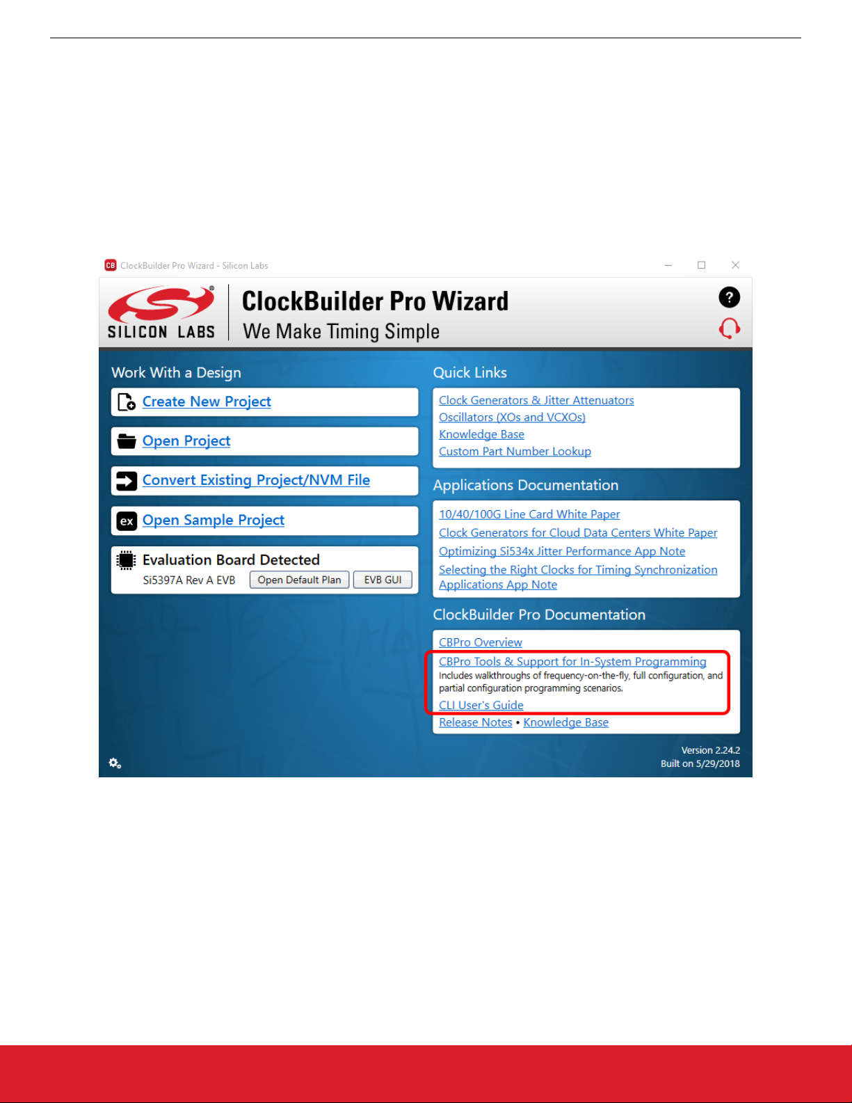
Si5397/96 Reference Manual
Frequency-On-The-Fly for Si5397/96
8. Frequency-On-The-Fly for Si5397/96
Some applications require characteristics like input frequency to be modified while leaving clocks from other DSPLLs unaffected. This
Frequency-On-The-Fly functionality is fully supported by Si5397 hardware with the help of CBPro Command Line Interface (CLI) tool.
Frequency-On-The-Fly allows user to:
• Reconfigure the input frequency, output frequency, bandwidth, and LOL/OOF thresholds of a certain DSPLL. The clock output of the
target DSPLL is disabled during the reconfiguration, but the functionalities (for example, freerun, holdover, lock acquisition, hitless
switching) remain the same after it is done.
• Leave all other DSPLLs undisturbed, which means that all clock functions, like phase noise and lock status, remain the same.
Detailed explanation on how to set up Frequency-On-The-Fly with CLI tool is included in these two documents: “CBPro Tools & Support
for In-System Programming” & “CLI User’s Guide”
Figure 8.1. CBPro Tools & Support for In-System Programming
The following steps outline the procedure to initiate Frequency-On-The-Fly:
1. Create CBPro project as base frequency plan.
2. Create text files detailing the input/output frequency, bandwidth, and/or LOL/OOF thresholds of new plans. Plans are defined independently for each PLL.
3. Use CLI FOTF tool (create a batch script) to auto generate register files for switching among different plans.
The CLI FOTF tool optimizes the VCO frequency for all of the plans “CLI User’s Guide” includes more in-depth and detailed syntax
explanation and function definition. Example files are bundled in CBPro at C:\Program Files (x86)\Silicon Laboratories\ClockBuilder Pro
\CLI\Samples\FOTF-For-Multi-PLL-Device.
silabs.com | Building a more connected world. Rev. 0.9 | 57
Page 58

Si5397/96 Reference Manual
Frequency-On-The-Fly for Si5397/96
For a more detailed information on this procedure, refer to “CBPro Tools & Support for In-System Programming” on the CBPro main
page. Note
error will be raised. The tool enforces this restriction.
FOTF can technically mean not changing input or output frequencies and instead only reconfiguring one of OOF, LOS or bandwidth. A
plan file only has to reconfigure *at least one* of the following:
Clock output frequency
Clock input frequency
DSPLL bandwidth
LOL thresholds
OOF thresholds
On multi-DSPLL devices, frequency-on -the-fly can only be performed on a PLL that has exclusive clock inputs. That is, an input to the
FOTF PLL cannot also be MUXed to another DSPLL. For example, given the following configuration:
Refer to AN1178: Frequency-On-the-Fly for Silicon Labs Jitter Attenuators and Clock Generators.
that the frequency plan cannot allow an input to be shared with multiple PLLs. If an input is shared across multiple PLLs an
silabs.com | Building a more connected world. Rev. 0.9 | 58
Page 59
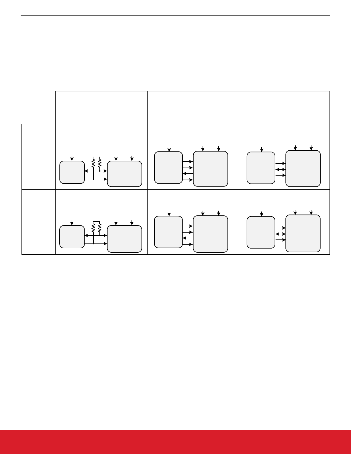
Si5397/96 Reference Manual
Serial Interface
9. Serial Interface
Configuration and operation of the Si5397/96 is controlled by reading and writing registers using the I2C or SPI serial interface. The
I2C_SEL pin selects between I2C or SPI operation. The Si5397/96 supports communication with either a 3.3 V or 1.8 V host by setting
the IO_VDD_SEL (0x0943[0]) configuration bit. The SPI mode supports 4-wire or 3-wire by setting the SPI_3WIRE configuration bit.
See the figure below for supported modes of operation and settings. The I2C pins are open drain and are ESD clamped to 3.3 V, regardless of the host supply level. The I2C pins are clamped to 3.3 V so that they may be externally pulled up to 3.3 V regardless of
IO_VDD_SEL (in register 0x0943).
The table below lists register settings of interest for the I2C/SPI.
2
I
C
SPI 4-Wire SPI 3-Wire
Host = 1.8V
Host = 3.3V
I2C_SEL pin = High
1.8V
2
I
C
SDA
HOST
SCLK
IO_VDD_SEL = 1 IO_VDD_SEL = 1 IO_VDD_SEL = 1
3.3V
2
I
C
SDA
HOST
SCLK
I2C_SEL pin = Low
SPI_3WIRE = 0
IO_VDD_SEL = 0
IO_VDD_SEL = 0
(Default) (Default)
1.8V
VDDA
VDDA
1.8V3.3V
VDD
Clock IC
1.8V3.3V
VDD
Clock IC
SPI
HOST
SPI
HOST
CSb
SDO
SDI
SCLK
3.3V
CSb
SDO
SDI
SCLK
1.8V
SDA
SCLK
3.3V
SDA
SCLK
Figure 9.1. I2C/SPI Device Connectivity Configurations
I2C_SEL pin = Low
SPI_3WIRE = 1
IO_VDD_SEL = 0
(Default)
1.8V3.3V
VDD
VDDA
CSb
SDI
SDO
SCLK
Clock IC Clock IC
1.8V3.3V
VDD
VDDA
CSb
SDI
SDO
SCLK
Clock IC
SPI
HOST
SPI
HOST
1.8V
CSb
SDIO
SCLK
3.3V
CSb
SDIO
SCLK
VDDA
CSb
SDIO
SCLK
VDDA
CSb
SDIO
SCLK
1.8V3.3V
VDD
1.8V3.3V
VDD
Clock IC
If neither serial interface is used, leave I2C_SEL unconnected. Pull pins SDA/SDIO, SCLK, A1/SDO, and A0/CS all low.
Note that the Si5397/96 is not I2C fail-safe upon loss of power. Applications that require fail-safe operation should isolate the device
from a shared I2C bus.
silabs.com | Building a more connected world. Rev. 0.9 | 59
Page 60
Si5397/96 Reference Manual
Serial Interface
Table 9.1. I2C/SPI Register Settings
Setting Name Hex Address [Bit Field] Function
Si5397/96
IO_VDD_SEL 0x0943[0] The IO_VDD_SEL configuration bit optimizes the VIL, VIH, VOL,
and VOH thresholds to match the VDDS voltage. By default the
IO_VDD_SEL bit is set to the VDD option. The serial interface
pins are always 3.3 V tolerant even when the device's VDD pin is
supplied from a 1.8 V source. When the I2C or SPI host is operat-
ing at 3.3 V and the Si5397/96 at VDD = 1.8 V, the host must
write the IO_VDD_SEL configuration bit to the VDDA option. This
will ensure that both the host and the serial interface are operating
at the optimum voltage thresholds.
SPI_3WIRE 0x002B[3] The SPI_3WIRE configuration bit selects the option of 4-wire or 3-
wire SPI communication. By default, this configuration bit is set to
the 4-wire option. In this mode the Si5397/96
commands from a 4-wire or 3- wire SPI host allowing configuration of device registers. For full bidirectional communication in 3wire mode, the host must write the SPI_3WIRE configuration bit to
“1”.
will accept write
silabs.com | Building a more connected world. Rev. 0.9 | 60
Page 61
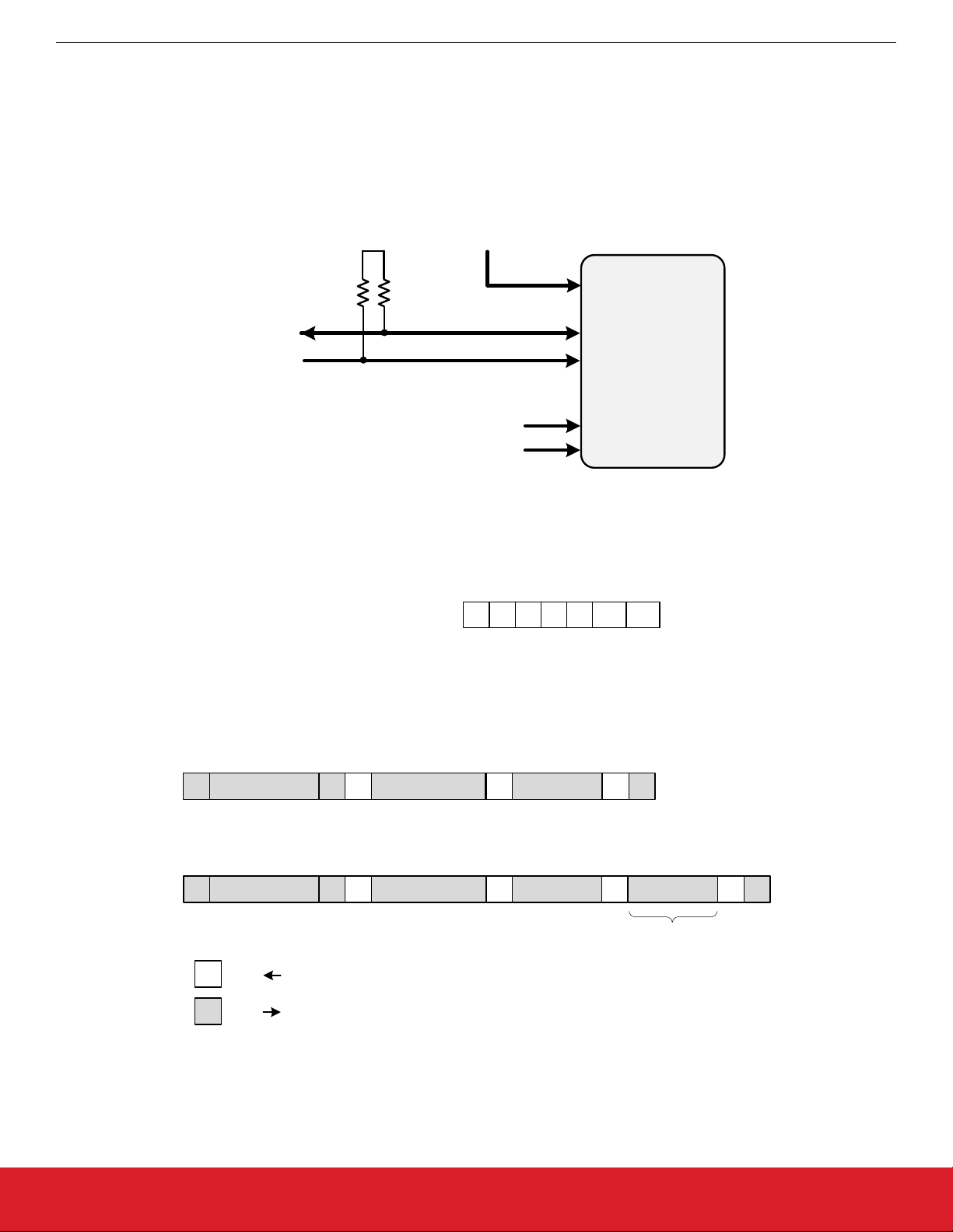
9.1 I2C Interface
Si5397/96 Reference Manual
Serial Interface
When in
Fast-Mode (400 kbps) and supports burst data transfer with auto address increments. The I2C bus consists of a bidirectional serial data
line (SDA) and a serial clock input (SCL) as shown in the figure below. Both the SDA and SCL pins must be connected to a supply via
an external pull-up (4.7 kΩ) as recommended by the I2C specification as shown in the figure below. Two address select bits (A0, A1)
are provided allowing up to four Si5397/96 devices to communicate on the same bus. This also allows four choices in the I2C address
for systems that may have other overlapping addresses for other I2C devices.
I2C mode, the serial interface operates in slave mode with 7-bit addressing and can operate in Standard-Mode (100 kbps) or
2
I
VDDI2C
VDD
C
I2C_SEL
2
To I
C Bus
or Host
Figure 9.2. I2C Configuration
The 7-bit slave device address of the Si5397/96 consists
as shown in the following figure.
LSBs of I
Address
of a 5-bit fixed address plus 2 pins which are selectable for the last two bits,
SDA
SCLK
2
C
A0
A1
Clock IC
0123456
Slave Address
Figure 9.3. 7-bit I2C Slave Address Bit-Configuration
Data is transferred MSB first in 8-bit words as specified by the I2C specification.
address + a write bit, an 8-bit register address, and 8 bits of data as shown in Figure 9.6 SPI Interface Connections on page 63. A
write burst operation is also shown where subsequent data words are written using to an auto-incremented address.
1 1 0 1 1 A0
A1
A write command consists of a 7-bit device (slave)
Write Operation – Single Byte
S 0 A Reg Addr [7:0]Slv Addr [6:0] A Data [7:0] PA
Write Operation - Burst (Auto Address Increment)
S 0 A Reg Addr [7:0]Slv Addr [6:0] A Data [7:0] A Data [7:0] PA
Reg Addr +1
1 – Read
Host
Clock IC
0 – Write
A – Acknowledge (SDA LOW)
Host
Clock IC
N – Not Acknowledge (SDA HIGH)
S – START condition
P – STOP condition
Figure 9.4. I2C Write Operation
A read operation is performed in two stages. A data write is used to set the register address, then a data read is performed to retrieve
the data from the set address. A read burst operation is also supported. This is shown in the following figure.
silabs.com | Building a more connected world. Rev. 0.9 | 61
Page 62
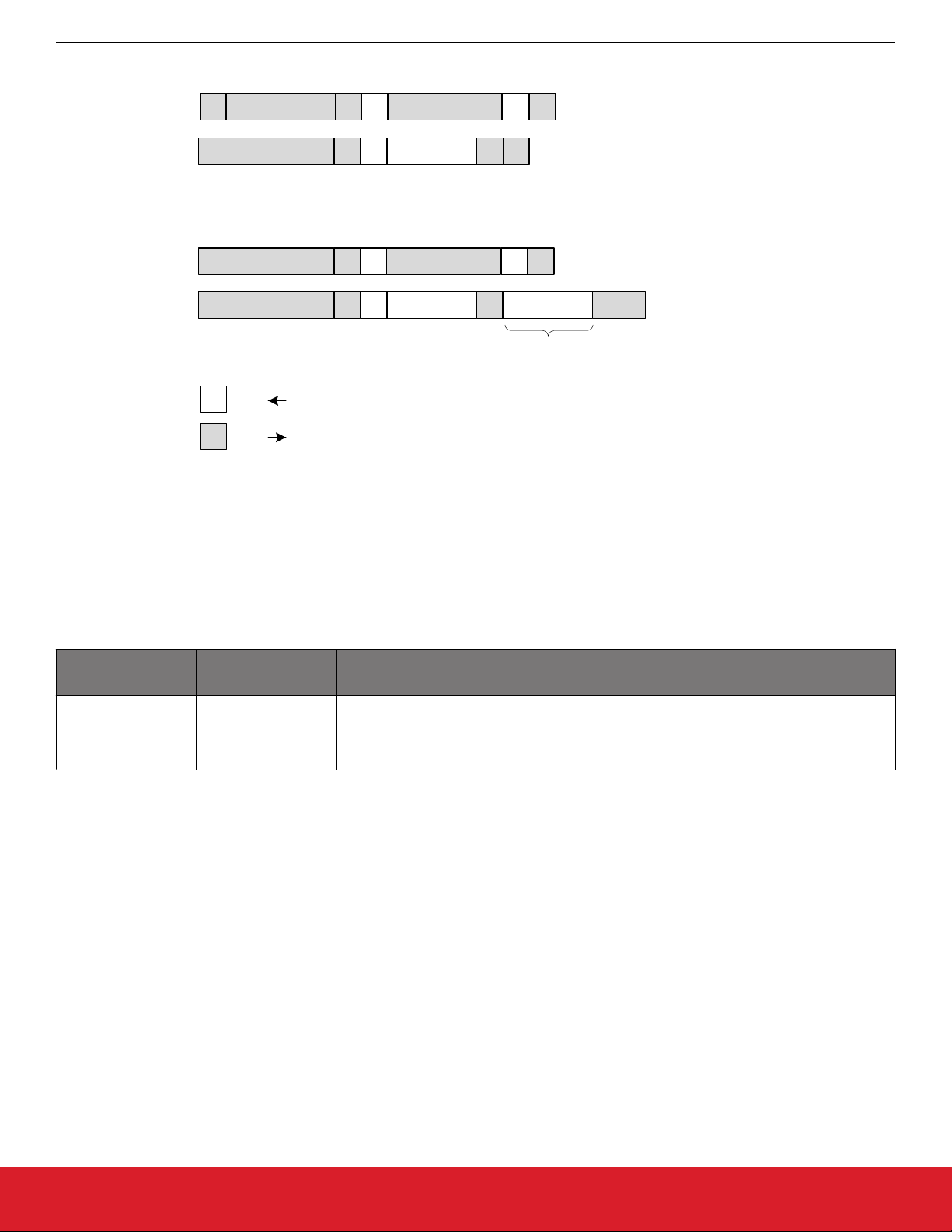
Read Operation – Single Byte
S 0 A Reg Addr [7:0]Slv Addr [6:0] A P
S 1 ASlv Addr [6:0] Data [7:0] PN
Read Operation - Burst (Auto Address Increment)
S 0 A Reg Addr [7:0]Slv Addr [6:0] A P
S 1 ASlv Addr [6:0] Data [7:0] A PNData [7:0]
Reg Addr +1
Si5397/96 Reference Manual
Serial Interface
Host
Clock IC
1 – Read
0 – Write
Host
Clock IC
A – Acknowledge (SDA LOW)
N – Not Acknowledge (SDA HIGH)
S – START condition
P – STOP condition
Figure 9.5. I2C Read Operation
The SMBUS interface requires a timeout. The error flags are found in the registers listed below.
Table 9.2. SMBus Timeout Error Bit Indicators
Register Name Hex Address [Bit
Field]
SMBUS_TIMEOUT 0x000C[5] 1 if there is a SMBus timeout error.
SMBUS_TIME-
OUT_FLG
0x0011[5] 1 if there is a SMBus timeout error.
Function
silabs.com | Building a more connected world. Rev. 0.9 | 62
Page 63
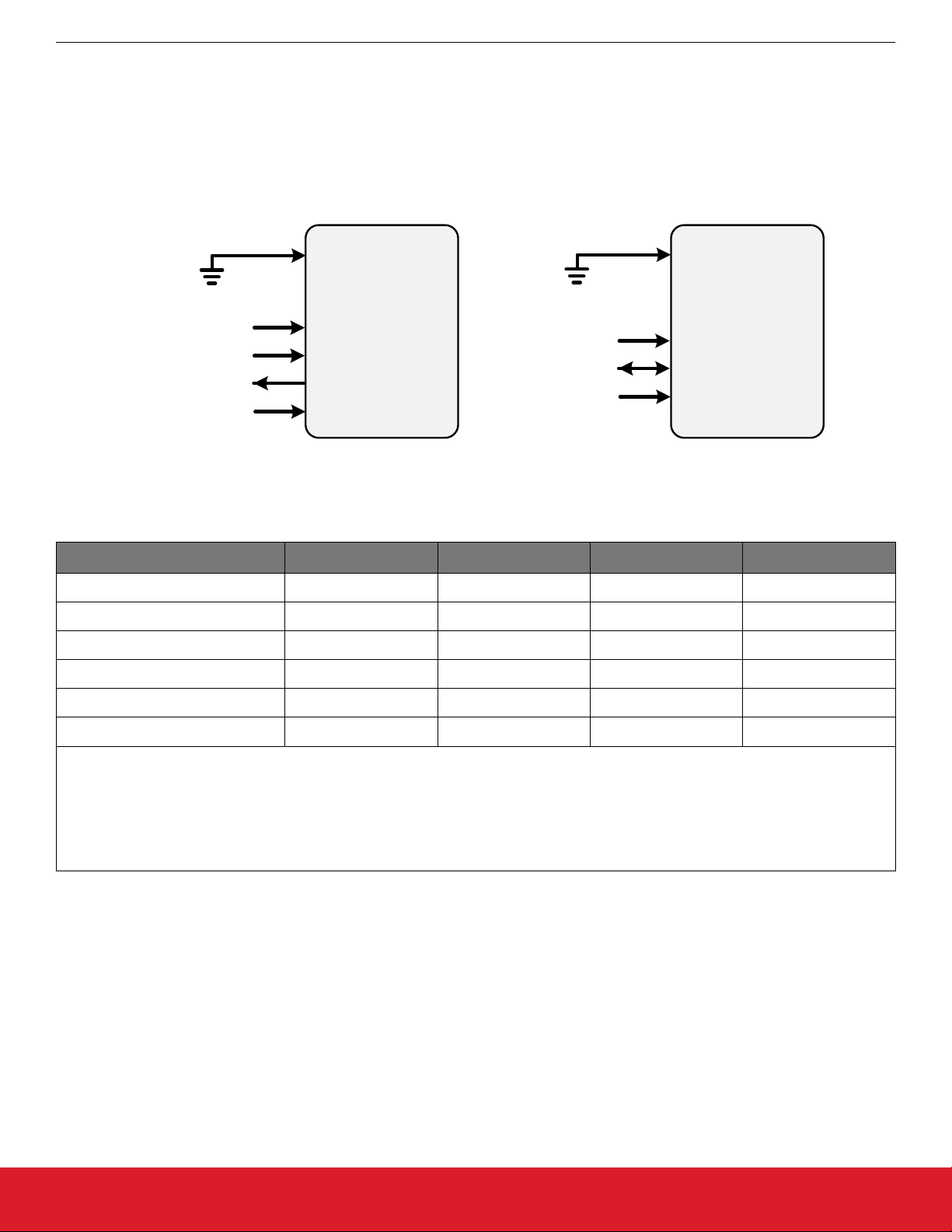
9.2 SPI Interface
Si5397/96 Reference Manual
Serial Interface
When in
wire interface consists of a clock input (SCLK), a chip select input (CS), serial data input (SDI), and serial data output (SDO). The 3wire interface combines the SDI and SDO signals into a single bidirectional data pin (SDIO). Both 4-wire and 3-wire interface connections are shown in the following figure.
SPI mode, the serial interface operates in 4-wire or 3-wire depending on the state of the SPI_3WIRE configuration bit. The 4-
SPI 3-Wire
SPI_3WIRE = 1
I2C_SEL
SPI 4-Wire
SPI_3WIRE = 0
I2C_SEL
CSb
CSb
To SPI
Host
SDI
SDO
To SPI
To SPI
Host
Host
SDIO
SCLK
SCLK
Clock IC
Figure 9.6. SPI Interface Connections
Table 9.3. SPI Command Format
Clock IC
Instruction
Set Address 000x xxxx 8-bit Address — —
Write Data 010x xxxx 8-bit Data — —
Read Data 100x xxxx 8-bit Data — —
Write Data + Address Increment 011x xxxx 8-bit Data — —
Read Data + Address Increment 101x xxxx 8-bit Data — —
Burst Write Data 1110 0000 8-bit Address 8-bit Data 8-bit Data
Note:
1.
X = don’t care (1 or 0).
2.
The Burst Write Command is terminated by de-asserting CSb (CSb = high).
3. There is no limit to the number of data bytes that follow the Burst Write Command, but the address will wrap around to zero in the
byte after address 255 is written.
Writing or reading data consist of sending a “Set Address” command followed by a “Write Data” or “Read Data” command. The 'Write
Data +
sequential address locations is necessary. The “Burst Write Data” instruction provides a compact command format for writing data
since it uses a single instruction to define starting address and subsequent data bytes. Figure 9.7 Example Writing Three Data Bytes
using the SPI Write Commands on page 64 shows an example of writing three bytes of data using the write commands. As can be
seen, the “Write Burst Data” command is the most efficient method for writing data to sequential address locations. Figure 9.8 Example
of Reading Three Data Bytes Using the SPI Read Commands on page 64 provides a similar comparison for reading data with the
read commands. Note that there is no equivalent burst read; the read increment function is used in this case.
Address Increment' or “Read Data + Address Increment” commands are available for cases where multiple byte operations in
Ist Byte
1
2nd Byte 3rd Byte Nth Byte
2,3
silabs.com | Building a more connected world. Rev. 0.9 | 63
Page 64
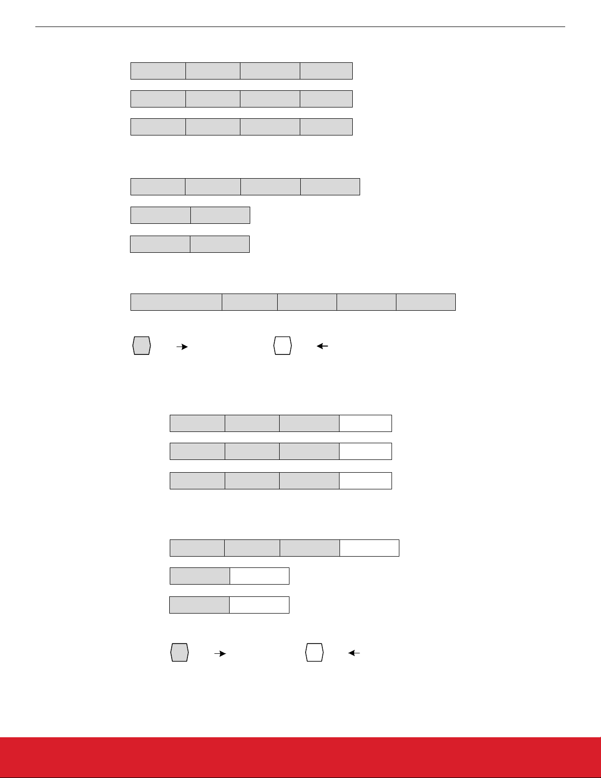
‘Set Address’ and ‘Write Data’
‘Set Addr’ Addr [7:0] ‘Write Data’ Data [7:0]
‘Set Addr’ Addr [7:0] ‘Write Data’ Data [7:0]
‘Set Addr’ Addr [7:0] ‘Write Data’ Data [7:0]
‘Set Address’ and ‘Write Data + Address Increment’
‘Set Addr’ Addr [7:0]
‘Write Data +
Addr Inc’
Data [7:0]
Si5397/96 Reference Manual
Serial Interface
‘Write Data +
Addr Inc’
‘Write Data +
Addr Inc’
Data [7:0]
Data [7:0]
‘Burst Write Data’
‘Burst Write Data’ Addr [7:0] Data [7:0] Data [7:0] Data [7:0]
Clock ICHost
Figure 9.7. Example Writing Three Data Bytes using the SPI Write Commands
Clock ICHost
‘Set Address’ and ‘Read Data’
‘Set Addr’ Addr [7:0] ‘Read Data’ Data [7:0]
‘Set Addr’ Addr [7:0] ‘Read Data’ Data [7:0]
‘Set Addr’ Addr [7:0] ‘Read Data’ Data [7:0]
‘Set Address’ and ‘Read Data + Address Increment’
‘Set Addr’ Addr [7:0] Data [7:0]
‘Read Data +
Addr Inc’
‘Read Data +
Addr Inc’
Figure 9.8. Example of Reading Three Data Bytes Using the SPI Read Commands
silabs.com | Building a more connected world. Rev. 0.9 | 64
Data [7:0]
Data [7:0]
Clock ICHost
‘Read Data +
Addr Inc’
Clock ICHost
Page 65
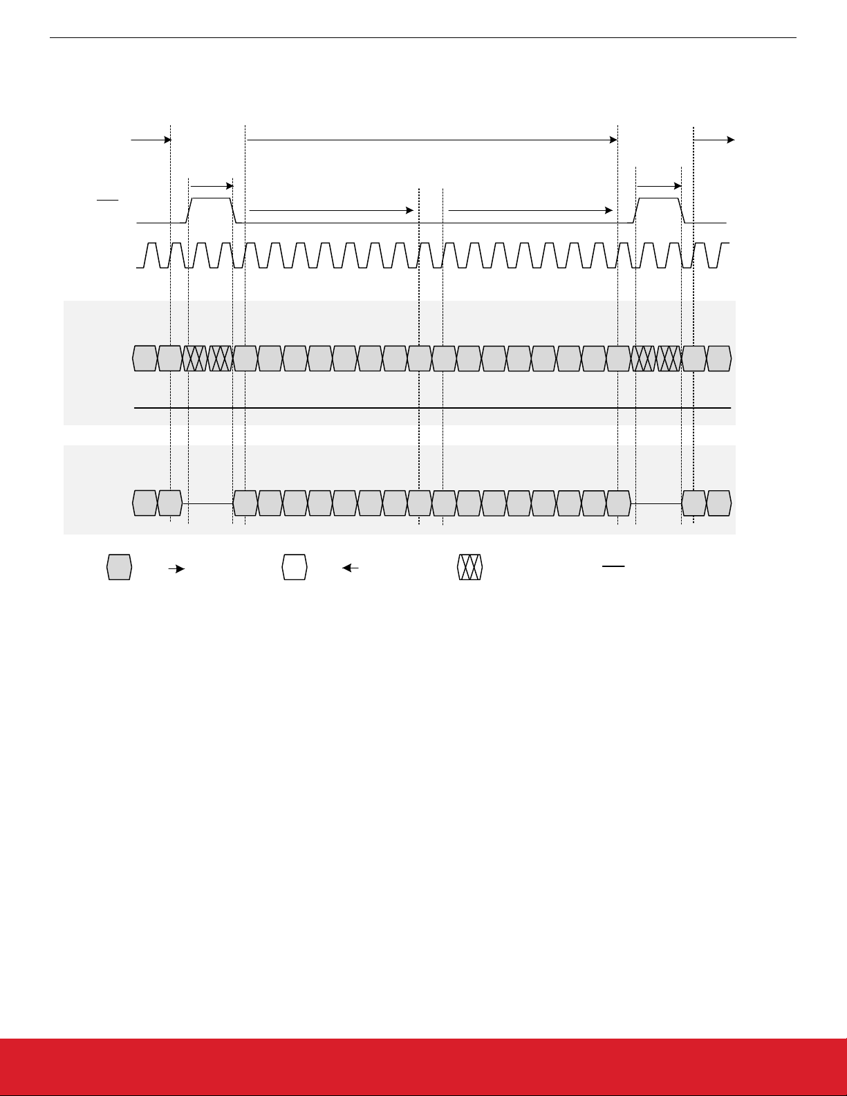
Si5397/96 Reference Manual
Serial Interface
The timing diagrams for the SPI commands are shown in Figures Figure 9.9
9.10 SPI “Write Data” and “Write Data+ Address Increment” Instruction Timing on page 66, Figure 9.11 SPI “Read Data” and “Read
Data + Address Increment” Instruction Timing on page 67, and Figure 9.12 SPI “Burst Data Write” Instruction Timing on page 67.
Previous
Command
>95 ns
‘Set Address’ Command
Set Address Instruction Base Address
SPI “Set Address” Command Timing on page 65, Figure
Next
Command
>95 ns
CS
SCLK
4-Wire
SDI
1
0
01234567
7
0123456
7
6
SDO
3-Wire
SDIO
1
0
Clock ICHost
Figure 9.9. SPI “Set Address” Command Timing
Clock ICHost
01234567
7
Don’t Care
0123456
High Impedance
7
6
silabs.com | Building a more connected world. Rev. 0.9 | 65
Page 66
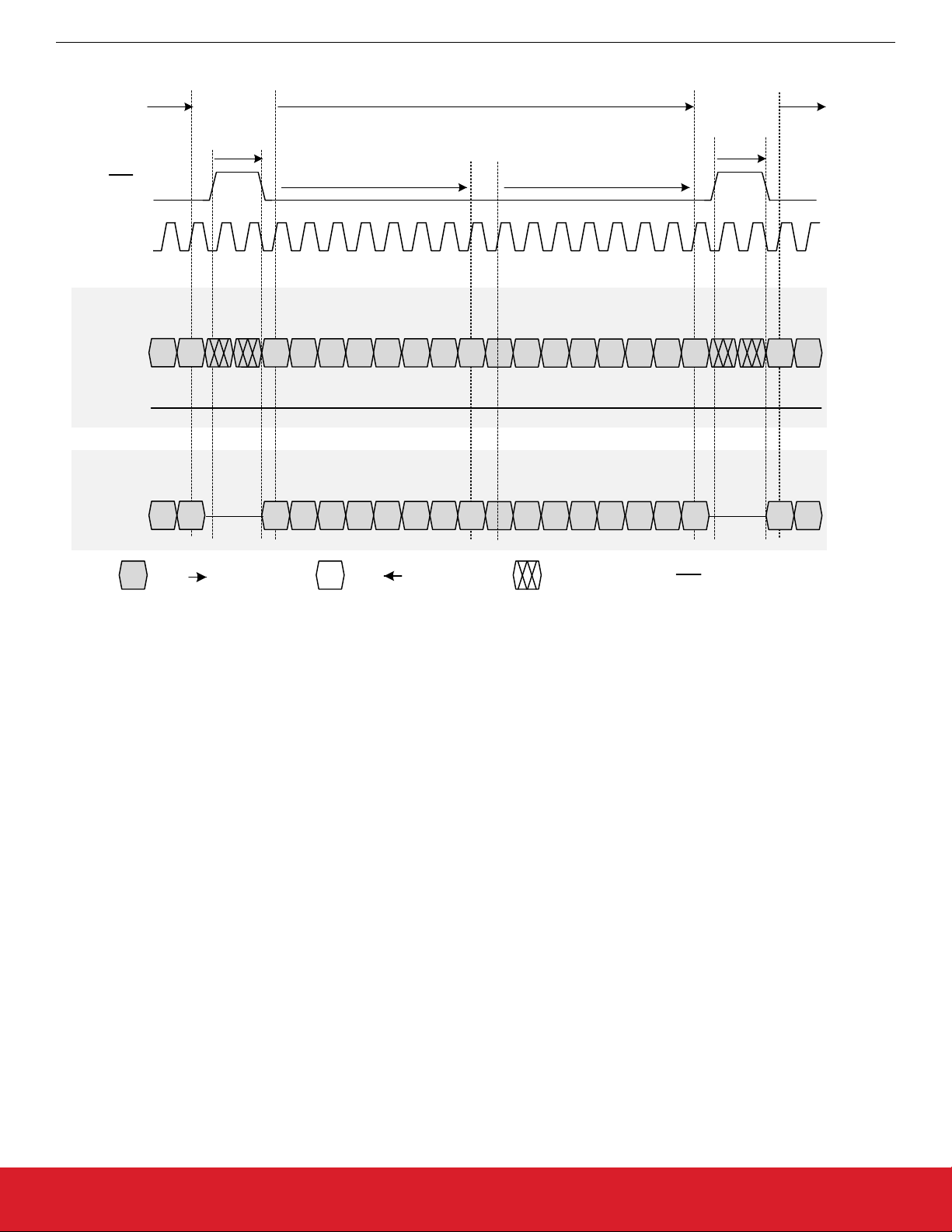
Si5397/96 Reference Manual
Serial Interface
Previous
Command
CS
SCLK
4-Wire
SDI
SDO
3-Wire
SDIO
‘Write Data’
>95 ns >95 ns
Write Data instruction
1
0
1
0
01234567
01234567
Data byte @ base address
or
Data byte @ base address + 1
01234567
01234567
Next
Command
7
6
7
6
Clock ICHost
Figure 9.10. SPI “Write Data” and “Write Data+ Address Increment” Instruction Timing
Clock ICHost
Don’t Care
High Impedance
silabs.com | Building a more connected world. Rev. 0.9 | 66
Page 67
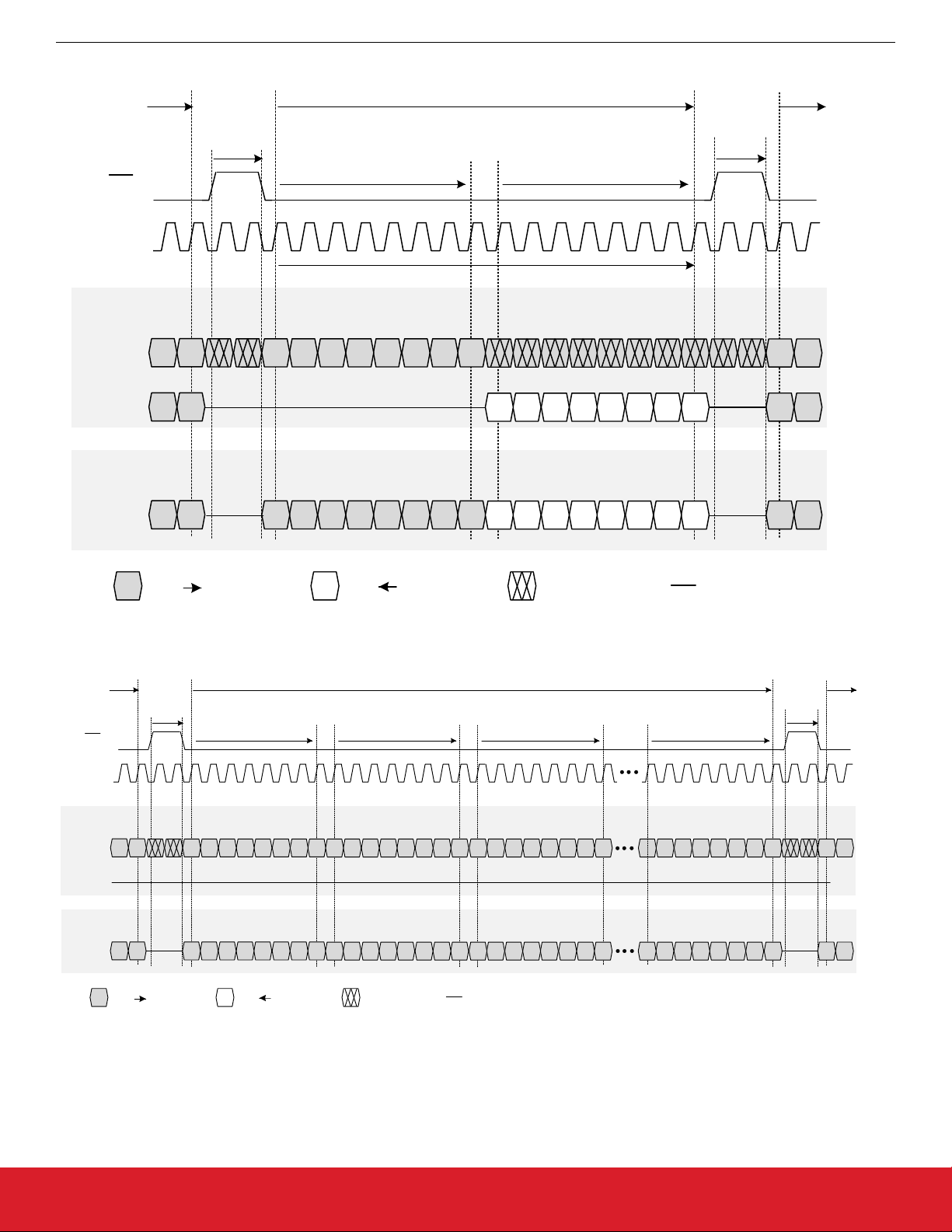
Si5397/96 Reference Manual
Serial Interface
Previous
Command
CS
SCLK
4-Wire
SDI
SDO
3-Wire
SDIO
‘Read Data’
>95 ns >95 ns
Read Data instruction
1
0
1
0
1
0
01234567
01234567
Read byte @ base address
or
Read byte @ base address +
1
01234567
01234567
Next
Command
7
6
7
6
7
6
Previous
Command
CS
SCLK
4-Wire
SDI
SDO
3-Wire
SDIO
Clock ICHost
Clock ICHost
Don’t Care
High Impedance
Figure 9.11. SPI “Read Data” and “Read Data + Address Increment” Instruction Timing
‘Burst Data Write’ Command
>95 ns >95 ns
Burst Write Instruction Base address
1
0
1
0
Clock ICHost
01234567
7
01234567
7 7 7
Clock ICHost
Don’t Care
st
1
data byte @ base address
0123456 0123456 01234567
7
0123456 0123456 0123456
High Impedance
n
th
data byte @ base address +n
Figure 9.12. SPI “Burst Data Write” Instruction Timing
Next
Command
7
6
7
6
Note that for all SPI communication the chip select (CS) must be high for the minimum time period between commands. When chip
select goes high it indicates the termination of the command. The SCLK can be turned off between commands, particularly if there are
very long delays between commands.
silabs.com | Building a more connected world. Rev. 0.9 | 67
Page 68
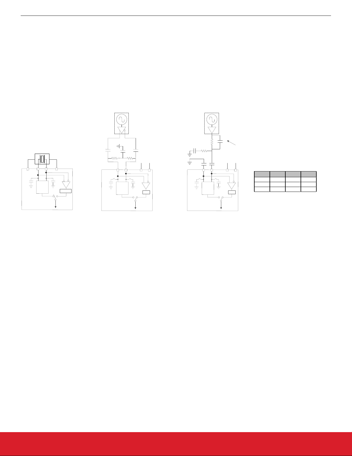
XO VDD R1 R2 C1
3.3V 453 Ω 549 Ω 12 pf
3.3V * 665 Ω 549 Ω 10 pf
2.5V 274 Ω 732 Ω 30 pf
Si5397/96 Reference Manual
XAXB References
10. XAXB References
10.1 External References
An external standard low-pullability crystal (XTAL) is recommended in combination with the internal oscillator (OSC) to produce an ultra
low phase noise reference clock for the DSPLL, as well as providing a stable reference for the Freerun and Holdover modes. Simplified
connection diagrams are shown below. The device includes internal 8 pF crystal loading capacitors which eliminates the need for external capacitors and also has the benefit of reduced noise coupling from external sources. In most applications, using the internal OSC
with an external crystal provides the best phase noise performance. See AN905: External References; Optimizing Performance for
more information on the performance of various XO's with these devices. The recommended crystal suppliers are listed in the
Si534x/8x Jitter Attenuators Recommended Crystal, TCXO and OCXOs Reference Manual.
0.1 uf
48-54 MHz
R2
0.1 uf
XB XA
XO/Clock
LVCMOS
R1
0.1 uf
C1
C1 is recommended
to increase
rate at Xa
nc nc
X1
X2
the slew
X2
48-54 MHz
XTAL
XB XA
Note: See Pin
Descriptions for
X1/X2 connections
X1
0.1 uf
48-54 MHz
XO/Clock
0.1 uf
50
XB XA
0.1 uf
50
nc nc
X1
X2
2xC
L
OSC
Crystal Resonator
Connection
(Recommended)
2xC
L
÷ PXAXB
Note: XA and XB must not exceed the maximum
2xC
L
Differential XO/Clock
Connection
(Not Recommended)
OSC
input voltage listed
2xC
2xC
L
÷ P
REF
in Si5372-71 Datasheet Table 5.3 Input Clock Specifications.
L
OSC
LVCMOS XO/Clock
Connection
(Not Recommended)
2xC
L
÷ P
REF
3.3V* These settings should be done if there CMOs level is
up to 4 V pp to limit the input at Xa to less than 2V ppse
Figure 10.1. XAXB Crystal Resonator and External Reference Clock Connection Options
In addition to crystal operations, the Si5397/96 accepts a clipped sine wave, CMOS, or differential reference clock on the XA/XB interface. Most clipped sine wave and CMOS TCXOs have insufficient drive strength to drive a 100 Ω or 50 Ω load. For this reason, place
the TCXO as close to the Si5397/96 as possible to minimize PCB trace length. In addition, ensure that both the Si5397/96 and the
TCXO are both connected directly to the ground plane. Figure 10.1 XAXB Crystal Resonator and External Reference Clock Connection
Options on page 68 shows the recommended method of connecting a clipped sine wave TCXO to the Si5397/96. Because the
Si5397/96 provides dc bias at the XA and XB pins, the ~800 mV peak-peak swing can be input directly into the XA interface of the
Si5397/96 once it has been ac-coupled. Because the signal is single-ended, the XB input is ac-coupled to ground. Figure 10.1 XAXB
Crystal Resonator and External Reference Clock Connection Options on page 68 illustrates the recommended method of connecting a
CMOS rail-to-rail output to the XA/XB inputs of the Si5397/96. The resistor network attenuates the rail-to-rail output swing to ensure that
the maximum input voltage swing at the XA pin is less than the data sheet specification. The signal is ac-coupled before connecting it to
the Si5397/96 XA input. Again, since the signal is single-ended, the XB input should be ac-coupled to ground. For applications with loop
BW values less than 10 Hz that require low wander output clocks, using a TCXO as the XAXB reference source should be considered
to avoid the wander of a crystal.
If an external oscillator is used as the XAXB reference, it is important to use a low jitter source because there is effectively no jitter
attenuation from the XAXB pins to the outputs. To minimize jitter at the XA/XB pins, the rise time of the XA/XB signals should be as fast
as possible.
For best jitter performance, use a XAXB frequency above 40 MHz. Also, for XAXB frequencies higher than 125 MHz, the PXAXB control must be used to divide the input frequency down below 125 MHz.
10.2 Recommended Crystals and Oscillators
Refer to the Recommended Crystal, TCXO, and OCXO Reference Manual for High-Performance Jitter Attenuators and Clock Genera-
tors for more information.
silabs.com | Building a more connected world. Rev. 0.9 | 68
Page 69
Si5397/96 Reference Manual
XAXB References
10.3 Register Settings to Configure for External XTAL Reference
The following registers can be used to control and make adjustments for the external reference source used.
10.3.1 XAXB_EXTCLK_EN Reference Clock Selection Register
Table 10.1. XAXB External Clock Selection Register
Setting Name Hex Address [Bit Field] Function
Si5397/96
XAXB_EXTCLK_EN 090E[0] Selects between the XTAL or external reference clock on the
XA/XB pins. Default is 0, XTAL. Set to 1 to use an external reference oscillator.
The internal crystal loading capacitors (CL) are disabled when an external clock source is selected.
10.3.2 PXAXB Pre-scale Divide Ratio for Reference Clock Register
Table 10.2. XAXB Pre-Scale Divide Ratio Register
Setting Name Hex Address [Bit Field] Function
Si5397/96
PXAXB 0x0206[1:0] Sets the XAXB input divider value according to the table below.
The following table lists the values, along with the corresponding divider ratio.
Table 10.3. XAXB Pre-Scale Divide Values
Value (Decimal) PXAXB Divider Value
0 1
1 2
2 4
3 8
silabs.com | Building a more connected world. Rev. 0.9 | 69
Page 70

Si5397/96 Reference Manual
Internal Reference
11. Internal Reference
Devices with internal reference (J/K/L/M) have a 48MHz crystal integrated in the package, to deliver a smaller layout footprint and more
immunity to acoustic emissions. This crystal is manufactured by a reliable Japanese crystal manufacturer and has been pre-screened
for activity dips before being assembled. It is important to note that connecting an external reference to XA/XB of a device that already
has an integrated reference is not allowed. Doing so could lead to internal damage to the circuits. When using this integrated crystal
option in a design that has been laid out for an external crystal, simply depopulate the crystal and replace the external crystal device
with the internal crystal version. It is important to note that a new CBPro plan is required for the integrated crystal variant. For more
information, please contact Silicon Labs support. For specifications of the internal crystal, please refer to the data sheet. During the
initial power up, the integrated crystal quickly settles down to a temperature that is slightly higher than ambient temperature due to proximity to the die. If the PLL is locked to an input, the frequency accuracy of the crystal has no impact on the output frequency accuracy; if
the PLL is free-running, then the output frequency tracks the crystal frequency which is still well within the spec.
silabs.com | Building a more connected world. Rev. 0.9 | 70
Page 71

Si5397/96 Reference Manual
Crystal, XO and Device Circuit Layout Recommendations
12. Crystal, XO and Device Circuit Layout Recommendations
The following are recommendations for crystal layout (for devices that require an external reference), as well as device layout for all
variants. The main layout issues that should be carefully considered include the following:
• Number and size of the ground vias for the Epad
• Output clock trace routing
• Input clock trace routing
• Control and Status signals to input or output clock trace coupling
• Xtal signal coupling (external reference devices)
• Xtal layout (external reference devices)
If the application uses a crystal for the XAXB inputs a shield should be placed underneath the crystal connected to the X1 and X2 pins
to provide the best possible performance. The shield should not be connected to the ground plane(s), and the layers underneath should
have as little area under the shield as possible. It may be difficult to do this for all the layers, but it is important to do this for the layers
that are closest to the shield.
Go to the Silicon Labs Clock Development Tool webpage to obtain Si5397, Si5396 evaluation board schematics, layouts, and component BOM files.
12.1 64-Pin QFN Si5397 Layout Recommendations
This section details the recommended guidelines for the external reference layout of the 64-pin Si5397 device using an example 8-layer
PCB. The following are the descriptions of each of the eight layers.
• Layer 1: device layer, with low speed CMOS control/status signals
• Layer 2: crystal shield (applies to external reference devices only)
• Layer 3: ground plane
• Layer 4: power distribution
• Layer 5: power routing layer
• Layer 6: input clocks
• Layer 7: output clocks layer
• Layer 8: ground layer
The 64 pin QFN crystal guidelines show the top layer layout of the Si5397 device mounted on the top PCB layer. This particular layout
was designed to implement either a crystal or an external oscillator as the XAXB reference. Note this applies only to external reference
devices. The crystal/ oscillator area is outlined with the white box around it. In this case, the top layer is flooded with ground. Note that
this layout has a resistor in series with each pin of the crystal. In typical applications, these resistors should be removed.
12.1.1 Si5397 XO Guidelines
For devices that use an external reference like an XO, pins X1 and X2 should not be connected to "ground" and should be left as "noconnects". An external reference does not need a crystal shield or the voids underneath the shield. The XA/XB connection should be
treated as a high speed critical path that is ac-coupled and terminated at the end of the etch run. The layout should minimize the stray
capacitance from the XA pin to the XB pin. Jitter is very critical at the XA/XB pins and therefore split termination and differential signaling should be used whenever possible.
silabs.com | Building a more connected world. Rev. 0.9 | 71
Page 72
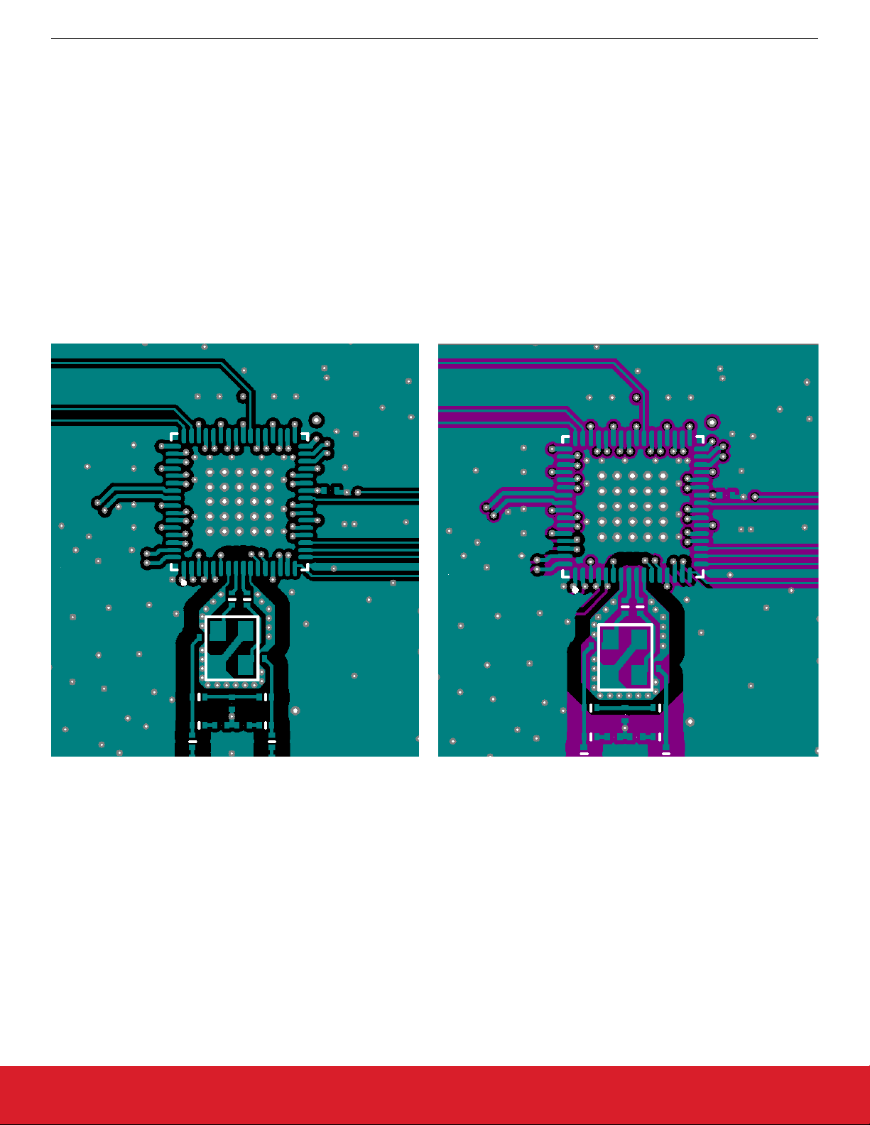
Crystal, XO and Device Circuit Layout Recommendations
12.1.2 Si5397 Crystal Guidelines
The following are five recommended crystal guidelines used with external reference devices:
1. Place the crystal as close as possible to the XA/XB pins.
2. DO NOT connect the crystal's GND pins to PCB gnd.
Si5397/96 Reference Manual
3. Connect
the crystal's GND pins to the DUT's X1 and X2 pins via a local crystal GND shield placed around and under the crystal. See
Figure 12.1 64-pin Si5397 Crystal Layout Recommendations Top Layer (Layer 1) on page 72 at the bottom left for an illustration of
how to create a crystal GND shield by placing vias connecting the top layer traces to the shield layer underneath. Note that a zoom
view of the crystal shield layer on the next layer down is shown in Figure 12.2 Zoom View Crystal Shield Layer, Below the Top Layer
(Layer 2) on page 73.
4. Minimize traces adjacent to the crystal/oscillator area especially if they are clocks or frequently toggling digital signals.
5. In general do not route GND, power planes/traces, or locate components on the other side, below the crystal GND shield. As an
exception if it is absolutely necessary to use the area on the other side of the board for layout or routing, then place the next reference
plane in the stack-up at least two layers away or at least 0.05 inches away. The Si5397 should have all layers underneath the ground
shield removed if possible.
Figure 12.1. 64-pin Si5397 Crystal Layout Recommendations Top Layer (Layer 1)
silabs.com | Building a more connected world. Rev. 0.9 | 72
Page 73
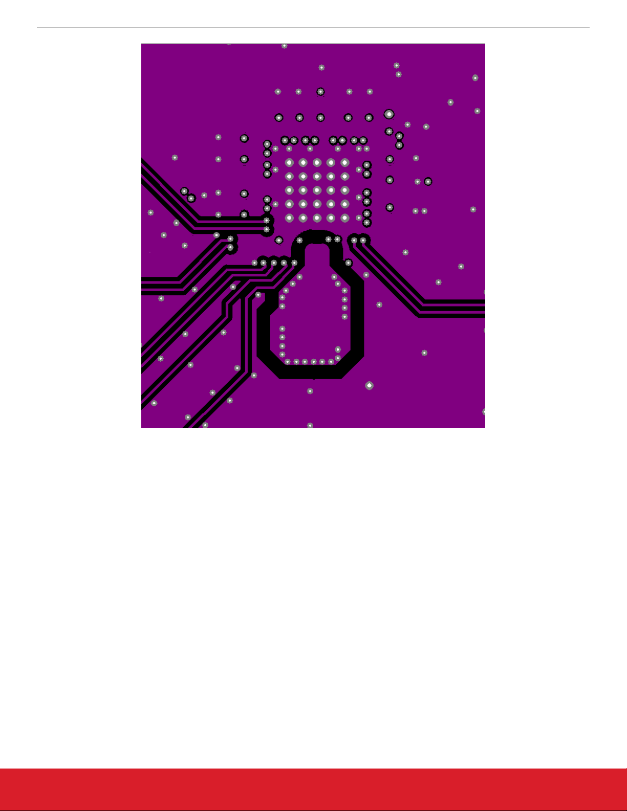
Si5397/96 Reference Manual
Crystal, XO and Device Circuit Layout Recommendations
Figure 12.2. Zoom View Crystal Shield Layer, Below the Top Layer (Layer 2)
Figure 12.2 Zoom View Crystal Shield Layer, Below the Top Layer (Layer 2) on page 73 shows the layer that implements the shield
underneath the crystal. The shield extends underneath the entire crystal and the X1 and X2 pins. This layer also has the clock input
pins. The clock input pins go to layer 2 using vias to avoid crosstalk. As soon as the clock inputs are on layer 2, they have a ground
shield above, below, and on the sides for protection.
Figure 12.3 Crystal Ground Plane (Layer 3) on page 74 is the ground plane and shows a void underneath the crystal shield. Figure
12.4 Power Plane (Layer 4) on page 75 is a power plane and shows the clock output power supply traces. The void underneath the
crystal shield is continued.
silabs.com | Building a more connected world. Rev. 0.9 | 73
Page 74
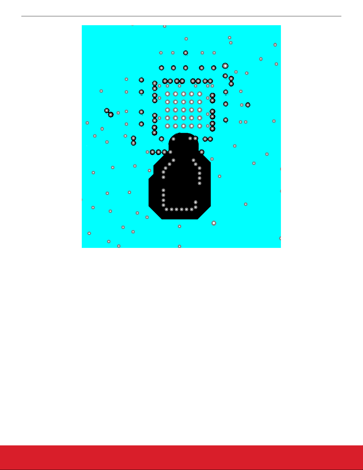
Si5397/96 Reference Manual
Crystal, XO and Device Circuit Layout Recommendations
Figure 12.3. Crystal Ground Plane (Layer 3)
silabs.com | Building a more connected world. Rev. 0.9 | 74
Page 75
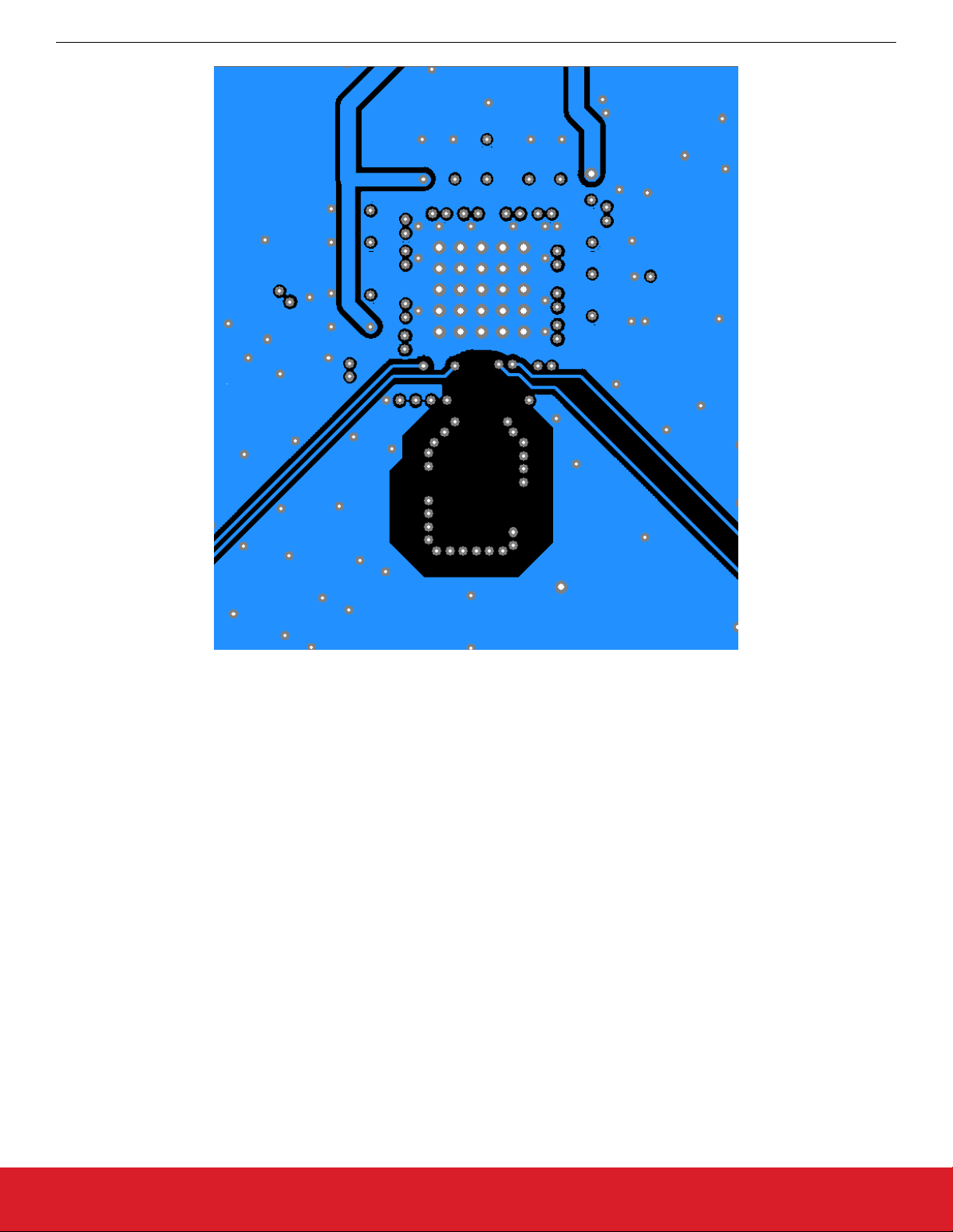
Si5397/96 Reference Manual
Crystal, XO and Device Circuit Layout Recommendations
Figure 12.4. Power Plane (Layer 4)
Figure 12.5 Layer 5 Power Routing on Power Plane (Layer 5) on page 76 shows layer 5, which is the power plane with the power
routed to the clock output power pins.
silabs.com | Building a more connected world. Rev. 0.9 | 75
Page 76
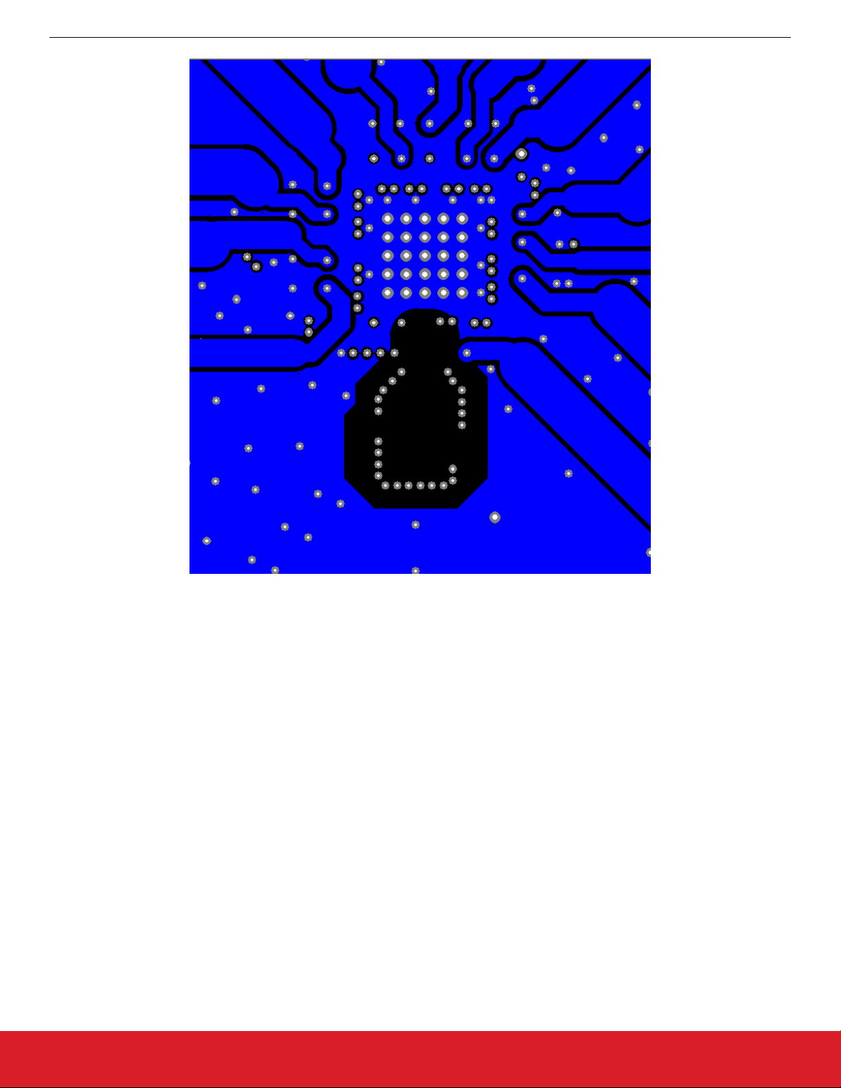
Si5397/96 Reference Manual
Crystal, XO and Device Circuit Layout Recommendations
Figure 12.5. Layer 5 Power Routing on Power Plane (Layer 5)
Figure 12.6 Ground Plane (Layer 6) on page 77 is another ground plane similar to layer 3.
silabs.com | Building a more connected world. Rev. 0.9 | 76
Page 77
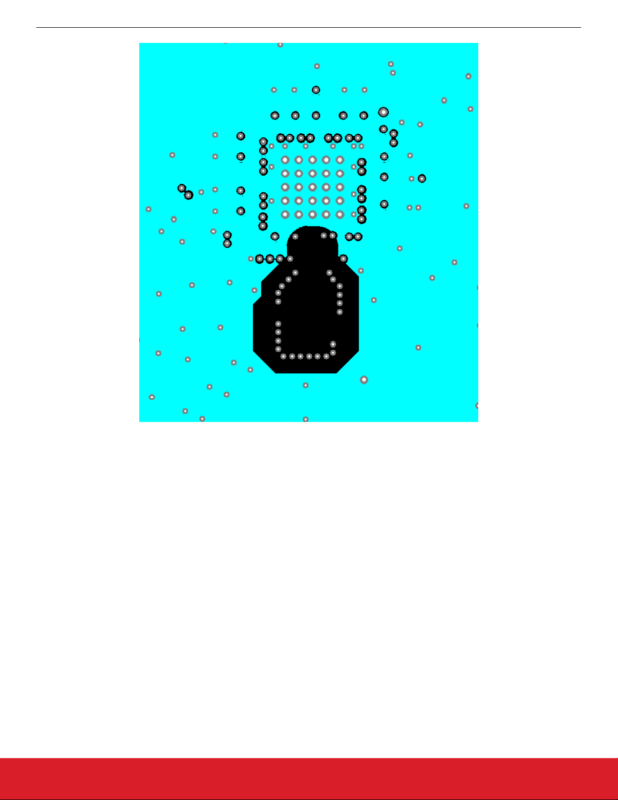
Si5397/96 Reference Manual
Crystal, XO and Device Circuit Layout Recommendations
Figure 12.6. Ground Plane (Layer 6)
silabs.com | Building a more connected world. Rev. 0.9 | 77
Page 78
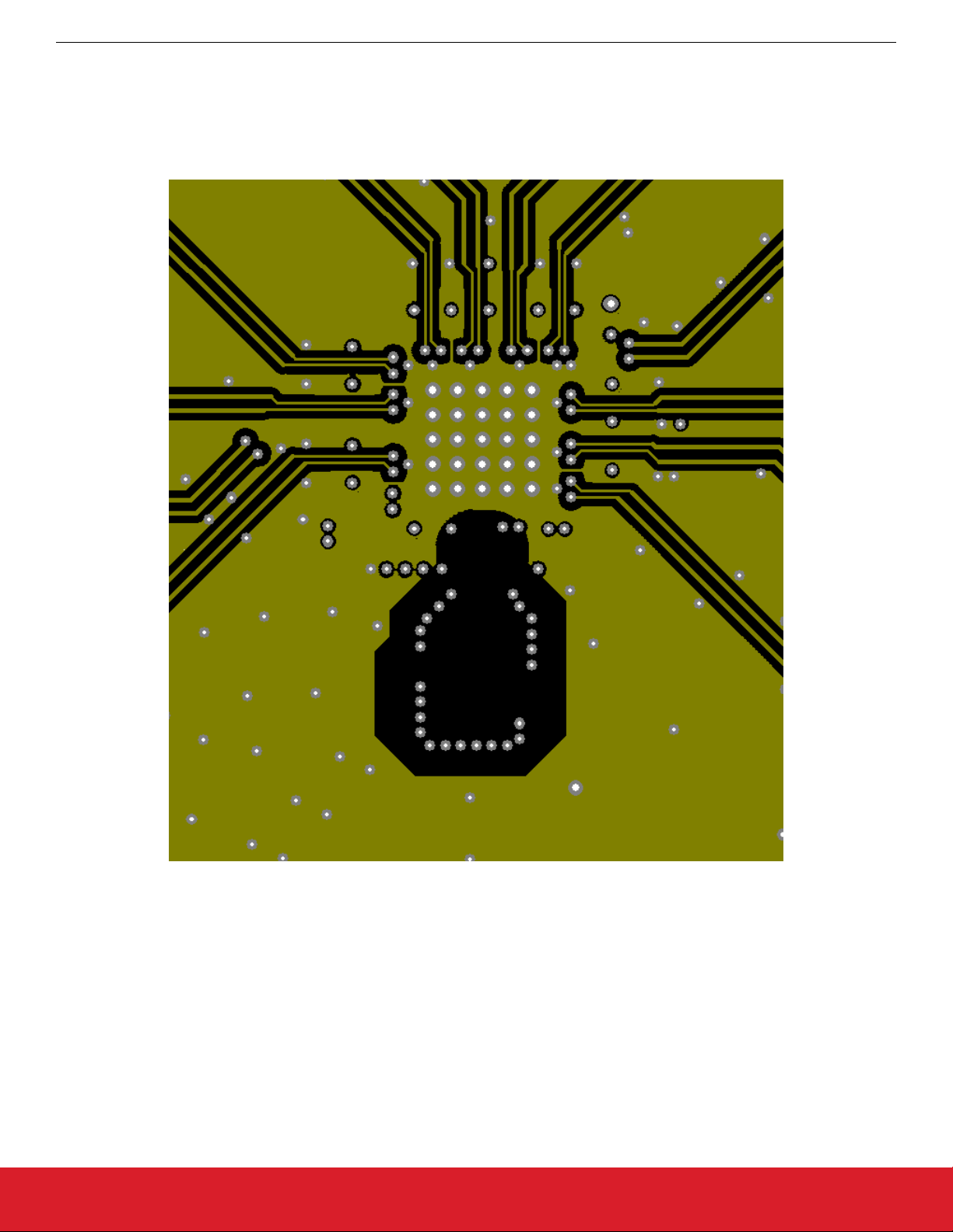
12.1.3 Si5397 Output Clocks
Si5397/96 Reference Manual
Crystal, XO and Device Circuit Layout Recommendations
Figure 12.7
Output Clock Layer (Layer 7) on page 78 shows the output clocks. Similar to the input clocks the output clocks have vias
that immediately go to a buried layer with a ground plane above them and a ground flooded bottom layer. There is a ground flooding
between the clock output pairs to avoid crosstalk. There should be a line of vias through the ground flood on either side of the output
clocks to ensure that the ground flood immediately next to the differential pairs has a low inductance path to the ground plane on layers
3 and 6.
Figure 12.7. Output Clock Layer (Layer 7)
silabs.com | Building a more connected world. Rev. 0.9 | 78
Page 79
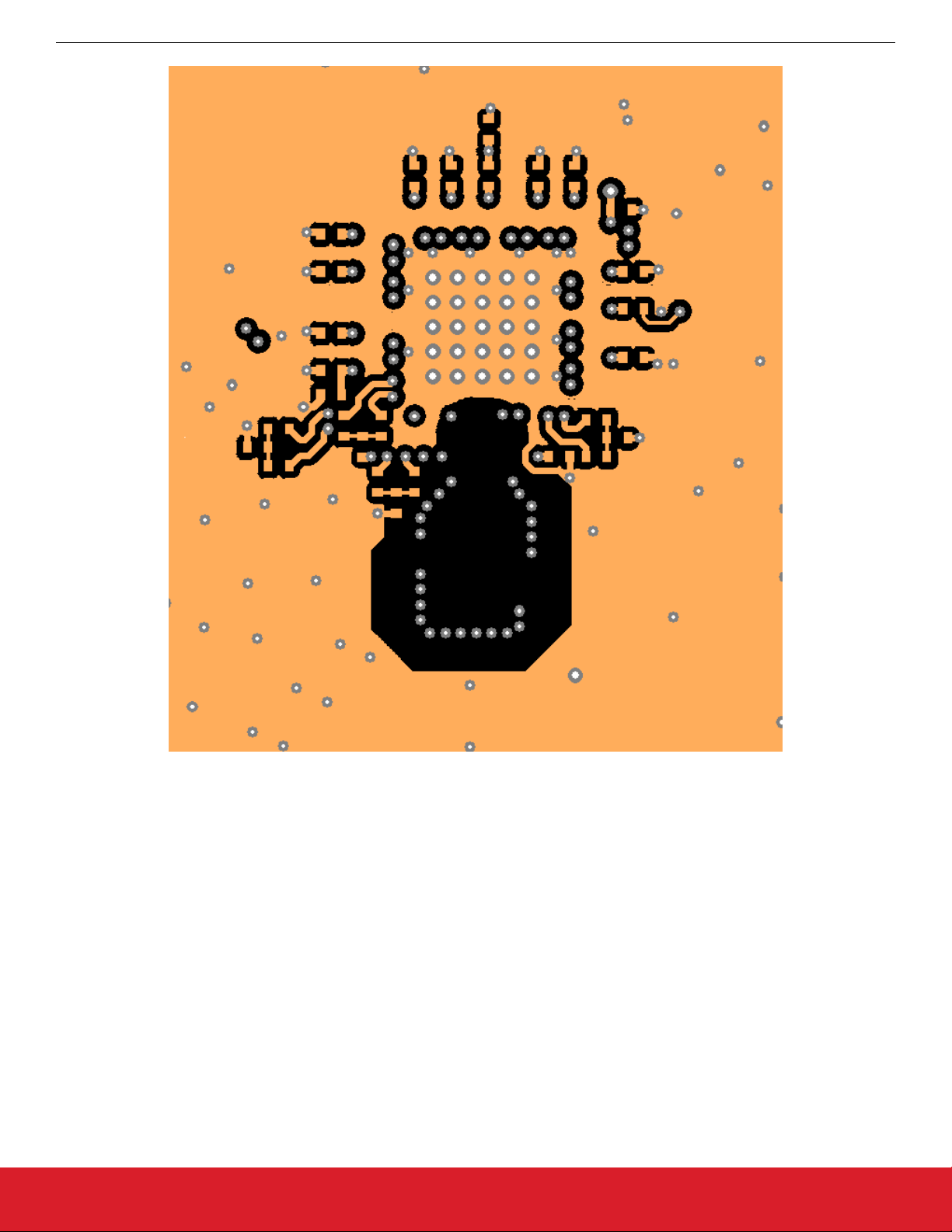
Si5397/96 Reference Manual
Crystal, XO and Device Circuit Layout Recommendations
Figure 12.8. Bottom Layer Ground Flooded (Layer 8)
12.2 64-Pin LGA Si5397
Layout Recommendations
This section details the recommended guidelines for the internal reference layout. The crystal is integrated inside the package so leave
XA, XB, X1, and X2 unconnected. An additional benefit of the internal crystal is that is does NOT need a crystal shield or voids on the
PCB layers beneath the crystal. It is recommended to minimize traces adjacent to the chip especially if there are clocks or frequently
toggling digital signals to avoid coupling of these signals into the device.
silabs.com | Building a more connected world. Rev. 0.9 | 79
Page 80

Si5397/96 Reference Manual
Crystal, XO and Device Circuit Layout Recommendations
12.3 44-Pin QFN Si5396 Layout Recommendations
This section details the layout recommendations for the 44-pin external reference devices using an example 6-layer PCB.
The following guidelines details images of a six layer board with the following stack:
Layer 1: device layer, with low speed CMOS control/status signals, ground flooded
Layer 2: crystal shield, output clocks, ground flooded
Layer 3: ground plane
Layer 4: power distribution, ground flooded
Layer 5: input clocks, ground flooded
Layer 6: low-speed CMOS control/status signals, ground flooded
This layout
was designed to implement either a crystal or an external oscillator as the XAXB reference (used with external reference
devics). The top layer is flooded with ground. The clock output pins go to layer 2 using vias to avoid crosstalk during transit. When the
clock output signals are on layer 2 there is a ground shield above, below and on all sides for protection. Output clocks should always be
routed on an internal layer with ground reference planes directly above and below. The plane that has the routing for the output clocks
should have ground flooded near the clock traces to further isolate the clocks from noise and other signals.
12.3.1 Si5396 XO Guidelines
For devices that use an external reference like an XO, pins X1 and X2 should not be connected to "ground" and should be left as "noconnects". An external reference does not need a crystal shield or the voids underneath the shield. The XA/XB connection should be
treated as a high speed critical path that is ac-coupled and terminated at the end of the etch run. The layout should minimize the stray
capacitance from the XA pin to the XB pin. Jitter is very critical at the XA/XB pins and therefore split termination and differential signaling should be used whenever possible. See Recommended Crystal, TCXO and OCXO Reference Manual for High-Performance Jitter
Attenuators and Clock Generators for a suggested list of XOs.
silabs.com | Building a more connected world. Rev. 0.9 | 80
Page 81
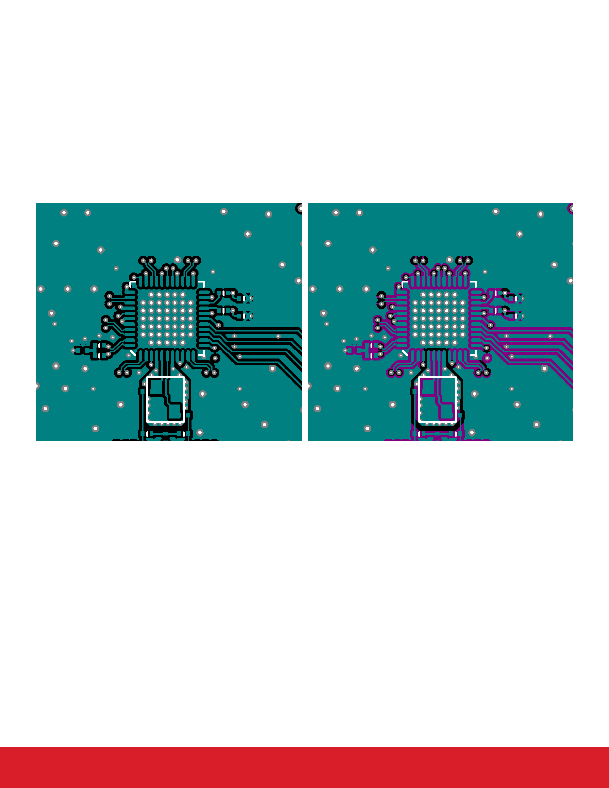
Si5397/96 Reference Manual
Crystal, XO and Device Circuit Layout Recommendations
12.3.2 Si5396 Crystal Guidelines
The following are five recommended crystal guidelines:
1. Place the crystal as close as possible to the XA/XB pins.
DO NOT connect the crystal's GND pins to PCB gnd.
2.
3. Connect the crystal's GND pins to the DUT's X1 and X2 pins via a local crystal GND shield placed around and under the crystal.
See Figure 12.9 Device Layer (Layer 1) on page 81 at the bottom left for an illustration of how to create a crystal GND shield by
placing vias connecting the top layer traces to the shield layer underneath. Note that a zoom view of the crystal shield layer on the
next layer down is shown in Figure 12.10 Crystal Shield Layer 2 on page 82.
4. Minimize traces adjacent to the crystal/oscillator area especially if they are clocks or frequently toggling digital signals.
5. In general do not route GND, power planes/traces, or locate components on the other side, below the crystal GND shield. As an
exception if it is absolutely necessary to use the area on the other side of the board for layout or routing, then place the next reference plane in the stack-up at least two layers away or at least 0.05 inches away. The Si5396 should have all layers underneath the
ground shield removed if possible.
Figure 12.9. Device Layer (Layer 1)
is
Figure 12.10 Crystal Shield Layer 2 on page 82
the second layer. The second layer implements the shield underneath the crystal.
The shield extends underneath the entire crystal and the X1 and X2 pins. There should be no less than 12 vias to connect the X1 and
X2 planes on layers 1 and 2. These vias are not shown in any other figures. All traces with signals that are not static must be kept well
away from the crystal and the X1 and X2 plane.
silabs.com | Building a more connected world. Rev. 0.9 | 81
Page 82
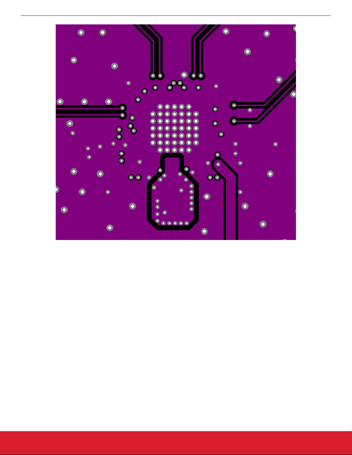
Si5397/96 Reference Manual
Crystal, XO and Device Circuit Layout Recommendations
Figure 12.10. Crystal Shield Layer 2
Figure 12.11 Ground Plane (Layer 3) on page 83 is the ground plane and shows a void underneath the crystal shield.
silabs.com | Building a more connected world. Rev. 0.9 | 82
Page 83
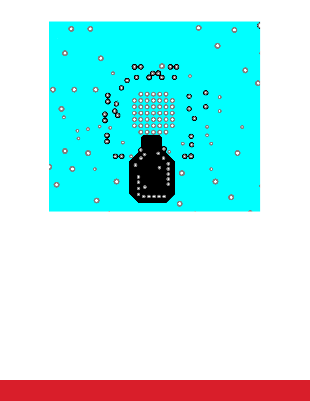
Si5397/96 Reference Manual
Crystal, XO and Device Circuit Layout Recommendations
Figure 12.11. Ground Plane (Layer 3)
Figure 12.12 Power Plane and Clock Output Power Supply Traces (Layer 4) on page 84 is a power plane showing the clock output
power supply traces. The void underneath the crystal shield is continued.
silabs.com | Building a more connected world. Rev. 0.9 | 83
Page 84
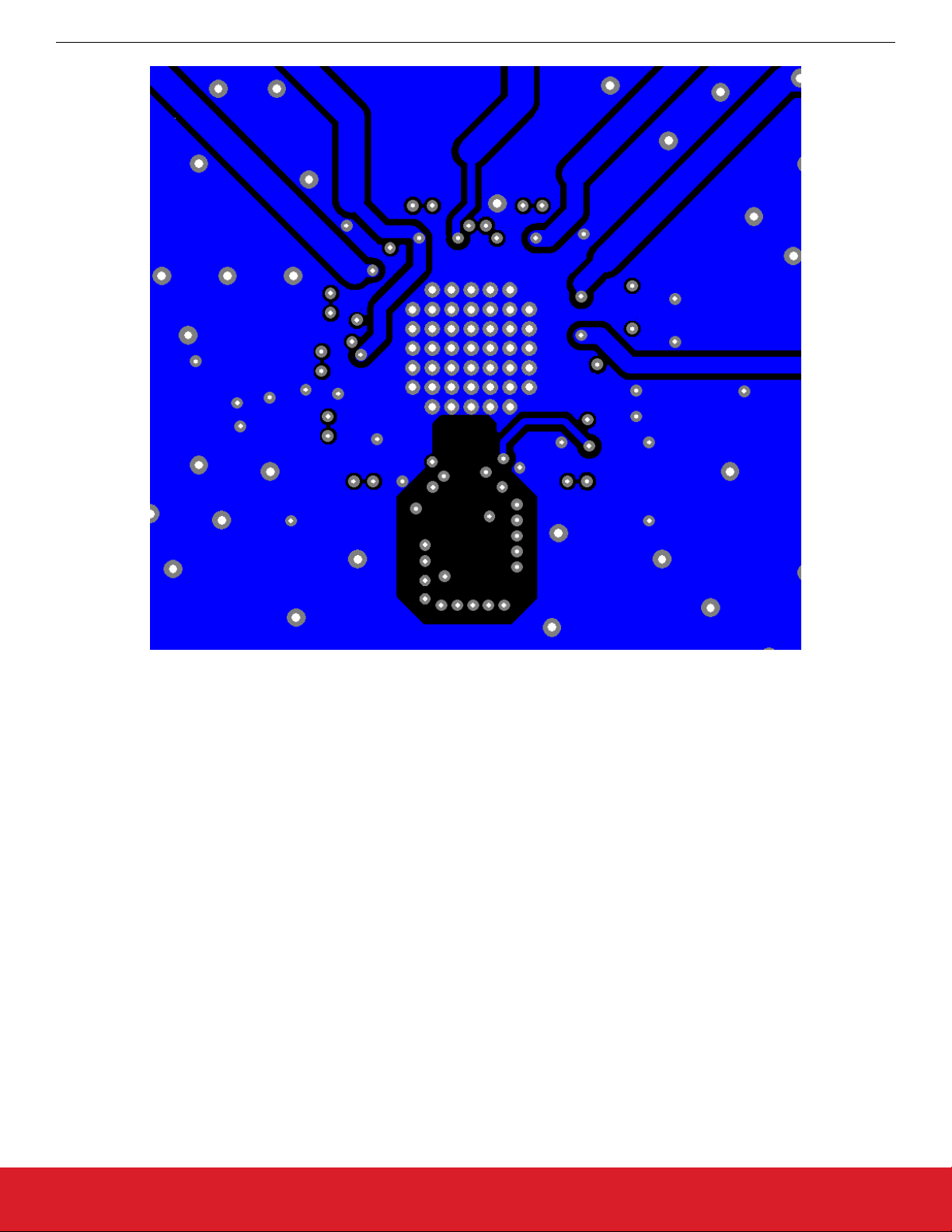
Si5397/96 Reference Manual
Crystal, XO and Device Circuit Layout Recommendations
Figure 12.12. Power Plane and Clock Output Power Supply Traces (Layer 4)
Figure 12.13 Clock Input Traces (Layer 5) on page 85 shows layer 5 and the clock input traces. Similar to the clock output traces,
they are routed to an inner layer and surrounded by ground to avoid crosstalk.
silabs.com | Building a more connected world. Rev. 0.9 | 84
Page 85
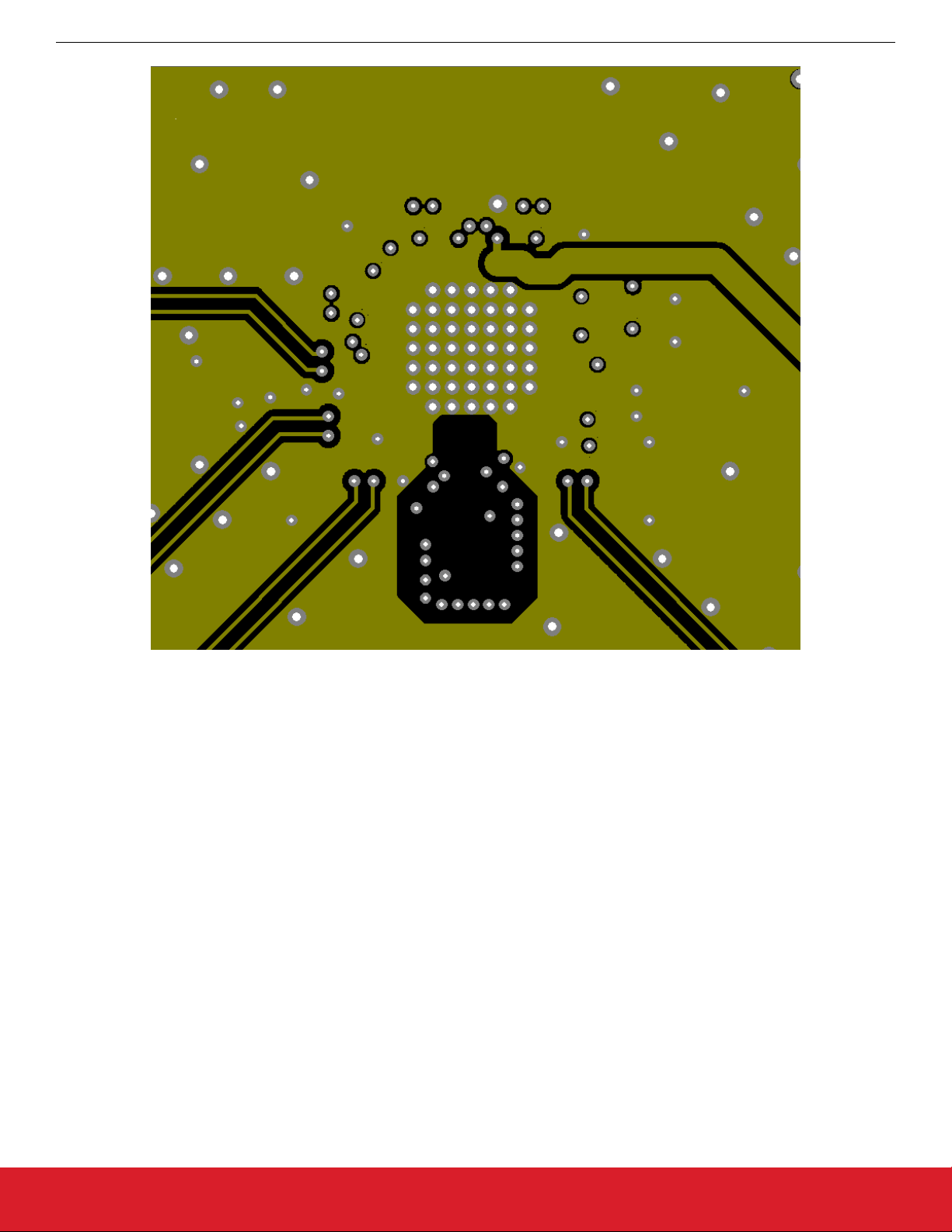
Si5397/96 Reference Manual
Crystal, XO and Device Circuit Layout Recommendations
Figure 12.13. Clock Input Traces (Layer 5)
Figure 12.14 Low-Speed CMOS Control and Status Signal Layer 6 (Bottom Layer) on page 86 shows the bottom layer, which contin-
ues the void underneath the shield. Layer 6 and layer 1 are mainly used for low speed CMOS control and status signals for which
crosstalk is not a significant issue. PCB ground can be placed under the XTAL Ground shield (X1/X2) as long as the PCB ground is at
least 0.05 inches below it.
silabs.com | Building a more connected world. Rev. 0.9 | 85
Page 86
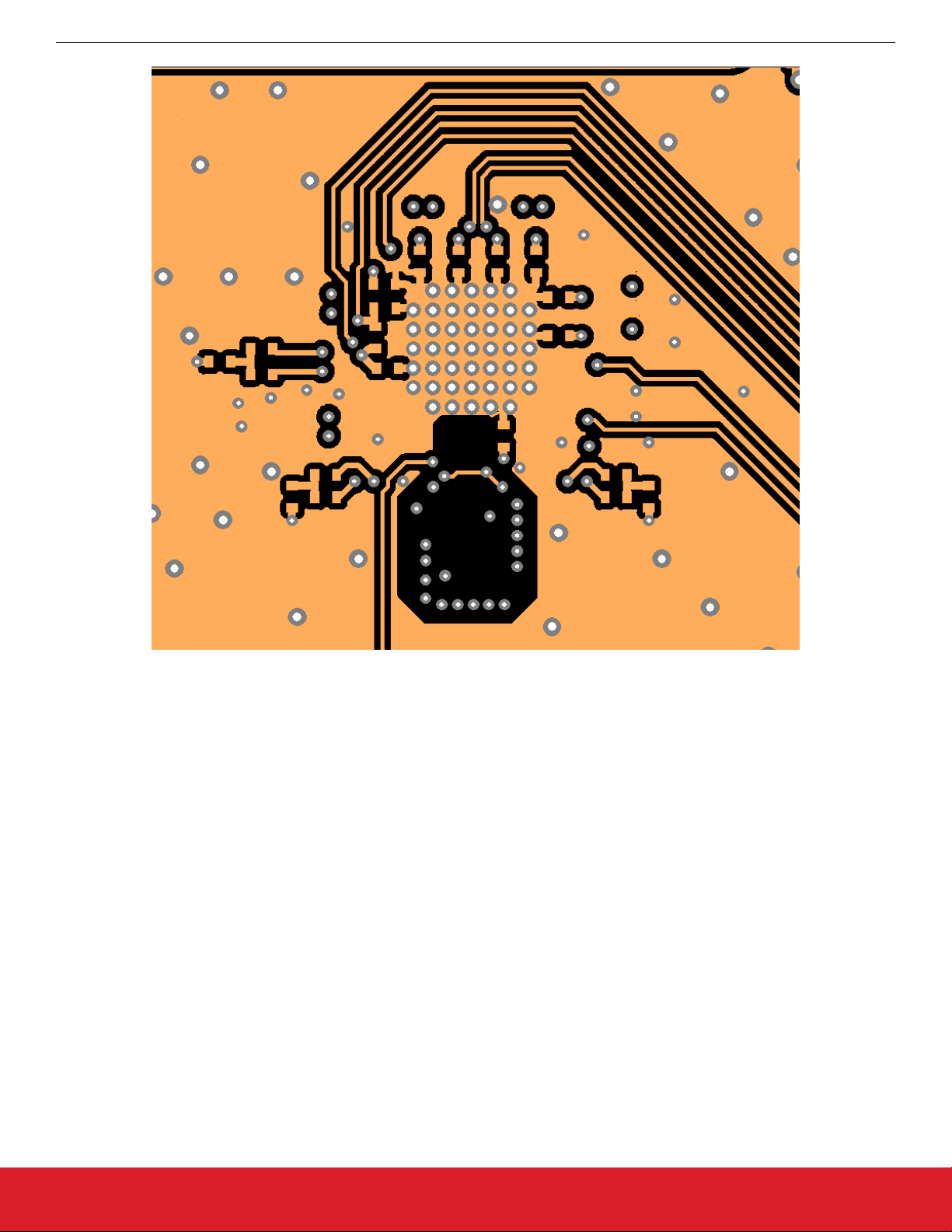
Si5397/96 Reference Manual
Crystal, XO and Device Circuit Layout Recommendations
Figure 12.14. Low-Speed CMOS Control and Status Signal Layer 6 (Bottom Layer)
For any high-speed, low-jitter application, the clock signal runs should be impedance-controlled to 100 Ω differential or 50 Ω singleended. Differential signaling is preferred because of its increased immunity to common-mode noise. All clock I/O runs should be properly terminated.
12.4 44-Pin LGA Si5396 Layout Recommendations
The crystal is integrated inside the package so leave XA, XB, X1, and X2 unconnected. An additional benefit of the internal crystal is
that is does NOT need a crystal shield or voids on the PCB layers beneath the crystal. It is recommended to minimize traces adjacent
to the chip especially if there are clocks or frequently toggling digital signals to avoid coupling of these signals into the device.
silabs.com | Building a more connected world. Rev. 0.9 | 86
Page 87
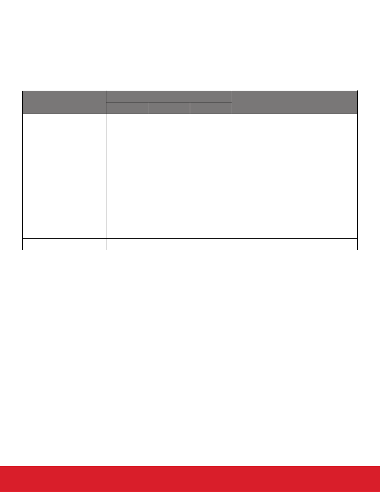
Si5397/96 Reference Manual
Power Management
13. Power Management
13.1 Power Management Features
Several unused functions can be powered down to minimize power consumption. The registers listed below are used for powering
down different features.
Table 13.1. Power-Down Registers
Setting Name Hex Address [Bit Field] Function
Si5397A/B Si5397C/D Si5396
PDN 0x001E[0] This bit allows powering down the device. The
serial interface remains powered during power
down mode and the registers are available to be
read and written.
OUT0_PDN
OUT1_PDN
OUT2_PDN
OUT3_PDN
OUT4_PDN
OUT5_PDN
OUT6_PDN
OUT7_PDN
OUT_PDN_ALL 0x0145[0] Power down all output drivers
13.2 Power Supply Recommendations
The power
regulation to minimize the impact of board level noise on clock jitter. Following conventional power supply filtering and layout techniques will further minimize signal degradation from the power supply.
It is recommended to use a 1 μF 0402 ceramic capacitor on each VDD for optimal performance. It is also suggested to include an optional, single 0603 (resistor/ferrite) bead in series with each supply to enable additional filtering if needed.
13.3 Power Supply Sequencing
supply filtering generally is important for optimal timing performance. The Si5397/96 devices have multiple stages of on-chip
0x0108[0]
0x0112[0]
0x0117[0]
0x011C[0]
0x0126[0]
0x012B[0]
0x0130[0]
0x013A[0]
0x0108[0]
0x011C[0]
0x0126[0]
0x012B[0]
—
—
—
—
0x0112[0]
0x0117[0]
0x0126[0]
0x012B[0]
—
—
—
—
Powers down unused clock outputs. When powered down, output pins will be high-impedance
with a light pull-down effect.
Four classes of supply voltages exist on the Si5397/96:
1. VDD = 1.8 V (Core digital supply)
2. VDDA = 3.3 V (Analog supply)
3. VDDOx = 1.8/2.5/3.3 V ± 5% (Clock output supply)
4. VDDS = 1.8/3.3V ± 5% (Digital I/O supply)
There is no requirement for power supply sequencing unless the output clocks are required to be phase aligned with each other. In this
case, the VDDO of each clock which needs to be aligned must be powered up before VDD and VDDA. VDDS has no effect on output
clock alignment.
If output-to-output alignment is required for applications where it is not possible to properly sequence the power supplies, then the output clocks can be aligned by asserting the SOFT_RST 0x001C[0] or Hard Reset 0x001E[1] register bits or driving the RSTB pin. Note
that using a hard reset will reload the register with the contents of the NVM and any unsaved changes will be lost.
One may observe that when powering up the VDD = 1.8 V rail first, that the VDDA = 3.3 V rail will initially follow the 1.8 V rail. Likewise,
if the VDDA rail is powered down first then it will not drop far below VDD until VDD itself is powered down. This is due to the pad I/O
circuits which have large MOSFET switches to select the local supply from either the VDD or VDDA rails. These devices are relatively
large and yield a parasitic diode between VDD and VDDA. Please allow for both VDD and VDDA to power-up and power-down before
measuring their respective voltages.
silabs.com | Building a more connected world. Rev. 0.9 | 87
Page 88

13.4 Grounding Vias
Si5397/96 Reference Manual
Power Management
The pad
on the bottom of the device functions as both the sole electrical ground and primary heat transfer path. Hence it is important to
minimize the inductance and maximize the heat transfer from this pad to the internal ground plane of the PCB. Use no fewer than 25
vias from the center pad to a ground plane under the device. In general, more vias will perform better. Having the ground plane near the
top layer will also help to minimize the via inductance from the device to ground and maximize the heat transfer away from the device.
silabs.com | Building a more connected world. Rev. 0.9 | 88
Page 89

Si5397/96 Reference Manual
Register Map
14. Register Map
14.1 Base vs. Factory Preprogrammed Devices
The Si5397/96 devices can be ordered as “base” or “factory-preprogrammed” (also known as “custom OPN”) versions.
14.2 “Base” Devices (a.k.a. “Blank” Devices)
Example “base” orderable part numbers (OPNs) are of the form “Si5397A-E-GM” or “Si5396B-E-GM”.
Base devices are available for applications where volatile reads and writes are used to program and configure the device for a particular application.
Base devices do not power up in a usable state (all output clocks are disabled).
Base devices are, however, configured by default to use a 48 MHz crystal on the XA/XB reference and a 1.8 V compatible I/O voltage
setting for the host I2C/SPI interface.
Additional programming of a base device is mandatory to achieve a usable configuration.
See the on-line lookup utility at: https://www.silabs.com/products/timing/lookup-customize to access the default configuration plan and
register settings for any base OPN.
14.3 “Factory Preprogrammed” (Custom OPN) Devices
Factory preprogammed devices use a “custom OPN”, such as Si5397A-E-xxxxx-GM, where xxxxx is a sequence of characters assigned by Silicon Labs for each customer-specific configuration. These characters are referred to as the “OPN ID”. Customers must
initiate custom OPN creation using the ClockBuilder Pro software.
Many customers prefer to order devices which are factory preprogrammed for a particular application that includes specifying the
XA/XB reference frequency/type, the clock input frequencies, the clock output frequencies, as well as the other options, such as automatic clock selection, loop BW, etc. The ClockBuilder software is required to select among all of these options and to produce a project
file which Silicon Labs uses to preprogram all devices with custom orderable part number (“custom OPN”).
Custom OPN devices contain all of the initialization information in their non-volatile memory (NVM) so that it powers up fully configured
and ready to go.
Because preprogrammed device applications are inherently quite different from one another, the default power up values of the register
settings can be determined using the custom OPN utility at: https://www.silabs.com/products/timing/lookup-customize.
Custom OPN devices include a device top mark which includes the unique OPN ID. Refer to the device data sheet's Ordering Guide
and Top Mark sections for more details.
Both “base” and “factory preprogrammed” devices can have their operating configurations changed at any time using volatile reads and
writes to the registers. Both types of devices can also have their current register configuration written to the NVM by executing an NVM
bank burn sequence (see Section 4.3 NVM Programming.)
silabs.com | Building a more connected world. Rev. 0.9 | 89
Page 90
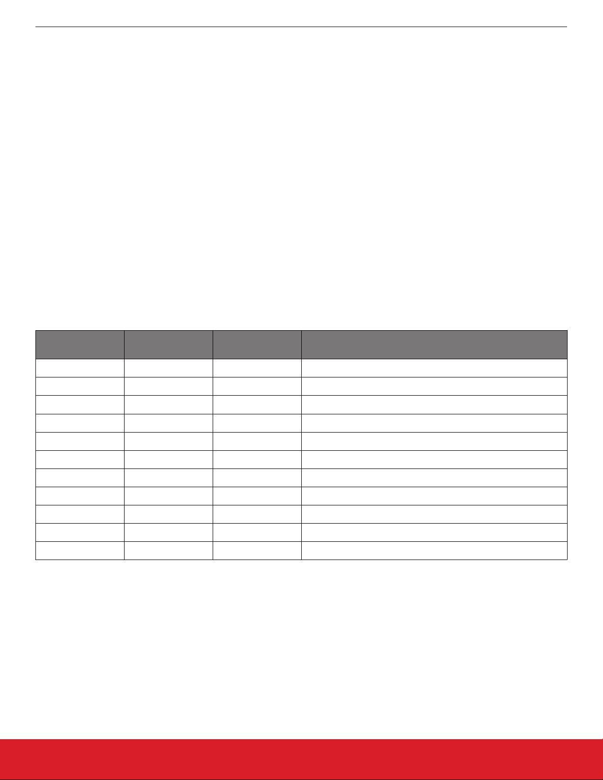
14.4 Register Map Overview and Default Settings Values
Si5397/96 Reference Manual
Register Map
The Si5397/96
family parts have large register maps that are divided into separate “Pages” of register banks. This allows more register
addresses than either the I2C or SPI serial interface standards 8-bit addressing provide. Each page has a maximum of 256 addresses,
however not all addresses are used on every page. Every register has a maximum data size of 8-bits, or 1 byte. Writing the page number to the 8-bit serial interface address of 0x01 on any page (0x0001, 0x0101, 0x0201, etc.) updates the page selection for subsequent
register reads and writes. For example, to access the value in register 0x040E, it is first necessary to write the page value 0x04 to serial
interface register address 0x01. At this point, the value of serial interface address 0x0E (0x040E) may be read or written. Note that is it
not necessary to write the page select register again when accessing other registers on the same page. Similarly, the read-only DEVICE_READY status is available from every page at serial interface address 0xFE (0x00FE, 0x01FE, 0x02FE, etc.).
It is recommended to use dynamic Read-Modify-Write methods when writing to registers which contain multiple settings, such as register 0x0011. To do this, first read the current contents of the register. Next, update only the select bit or bits that are being modified. This
may involve using both logical AND and logical OR operations. Finally, write the updated contents back to the register. Writing to pages, registers, or bits not documented below may cause undesired behavior in the device.
Details of the register and settings information are organized hierarchically below. To find the relevant information for your application,
first choose the section corresponding to the base part number, Si5397, Si5396 for your design. Then, choose the section under that for
the page containing the desired register(s).
Default register contents and settings differ for each device part number, or OPN. This information may be found by searching for the
Custom OPN for your device using the link below. Both Base/Blank and Custom OPNs are available there. See the previous section on
“Base vs. Factory Preprogrammed Devices" for more information on part numbers. The Private Addendum to the datasheet lists the
default settings and frequency plan information. You must be logged into the Silicon Labs website to access this information. The Public
addendum gives only the general frequency plan information (https://www.silabs.com/products/timing/lookup-customize).
Table 14.1. Register Map Paging Descriptions
Page Start Address (Hex) Start Address (Dec-
Contents
imal)
Page 0 0000h 0 Alarms, interrupts, reset, and other configuration
Page 1 0100h 256 Output clock configuration
Page 2 0200h 512 P and R dividers, user scratch area
Page 3 0300h 768 Internal divider value updates
Page 4 0400h 1024 DSPLLA
Page 5 0500h 1280 DSPLLB
Page 6 0600h 1536 DSPLLC, Si5397 only
Page 7 0700h 1792 DSPLLD, Si5397 only
Page 9 0900h 2304 Control IO configuration
Page A 0A00h 2560 Internal divider enables
Page B 0B00h 2816 Internal clock disables and control
R = Read Only
R/W = Read Write
S = Self Clearing
A self-clearing
bit will be cleared by the device once the operation initiated by this bit is complete. Registers with “sticky” flag bits, such
as LOS0_FLG, are cleared by writing “0” to the bit that has been automatically set high by the device.
silabs.com | Building a more connected world. Rev. 0.9 | 90
Page 91
Si5397/96 Reference Manual
Si5397A/B Register Map
15. Si5397A/B Register Map
15.1 Page 0 Registers Si5397A/B
Table 15.1. 0x0000 Die Rev
Reg Address Bit Field Type Setting Name Description
0x0000 3:0 R DIE_REV 4- bit Die Revision Number
Table 15.2. 0x0001 Page
Reg Address Bit Field Type Setting Name Description
0x0001 7:0 R/W PAGE Selects one of 256 possible pages.
The “Page Select” register is located at address 0x01 on every page. When read, it indicates the current page. When written, it will
change the page to the value entered. There is a page register at address 0x0001, 0x0101, 0x0201, 0x0301, … etc.
Table 15.3. 0x0002–0x0003 Base Part Number
Reg Address Bit Field Type Setting Name Value Description
0x0002 7:0 R PN_BASE 0x47 Four-digit “base” part number, one nibble per
0x0003 15:8 R PN_BASE 0x53
Table 15.4. 0x0004 Device Grade
Reg Address Bit Field Type Setting Name Description
0x0004 7:0 R GRADE One ASCII character indicating the device speed/
synthesis mode.
0 = A
1 = B
2 = C
3 = D
10=J, 11=K, 12=L, 13=M
Refer to the device data sheet Ordering Guide section for more information about device grades.
digit
Example: Si5397
ber (OPN) is 5397
ter
A-A-GM. The base part num-
, which is stored in this regis-
Table 15.5. 0x0005 Device Revision
Reg Address Bit Field Type Setting Name Description
0x0005 7:0 R DEVICE_REV One ASCII character indicating the device revision lev-
el.
0 = A; 1 = B, etc.
Example Si5397
“A” and stored as 0
silabs.com | Building a more connected world. Rev. 0.9 | 91
C-A12345-GM, the device revision is
Page 92
Si5397/96 Reference Manual
Si5397A/B Register Map
Table 15.6. 0x0006–0x0008 TOOL_VERSION
Reg Address Bit Field Type Name Description
0x0006 3:0 R/W TOOL_VERSION[3:0] Special
0x0006 7:4 R/W TOOL_VERSION[7:4] Revision
0x0007 7:0 R/W TOOL_VERSION[15:8] Minor[7:0]
0x0008 0 R/W TOOL_VERSION[15:8] Minor[8]
0x0008 4:1 R/W TOOL_VERSION[16] Major
0x0008 7:5 R/W TOOL_VERSION[13:17] Tool. 0 for ClockBuilder Pro
Table 15.7. 0x0009–0x000A NVM Identifier, Pkg ID
Reg Address Bit Field Type Setting Name Description
0x0009 7:0 R TEMP_GRADE Device temperature grading
0 = Industrial (–40 °C to 85 °C) ambient conditions
0x000A 7:0 R PKG_ID Package ID
0 = 9x9 mm 64 QFN
Part numbers are of the form:
Si<Part Num Base><Grade>-<Device Revision><OPN ID>-<Temp Grade><Package ID>
Examples:
C-A12345-GM.
Si5397
Applies
to a “base” or “blank” OPN (Ordering Part Number) device. These devices are factory pre-programmed with the frequency plan
and all other operating characteristics defined by the user’s ClockBuilder Pro project file.
Si5397C-A-GM.
Applies to a “base” or “blank” OPN device. Base devices are factory pre-programmed to a specific base part type (e.g., Si5397 but
exclude any user-defined frequency plan or other user-defined operating characteristics selected in ClockBuilder Pro.
Table 15.8. 0x000B I2C Address
Reg Address Bit Field Type Setting Name Description
0x000B 6:0 R/W I2C_ADDR 7-bit I2C Address. Note: This register is not bank burna-
ble.
Table 15.9. 0x000C Internal Status Bits
Reg Address Bit Field Type Setting Name Description
0x000C 0 R SYSINCAL 1 if the device is calibrating.
0x000C 1 R LOSXAXB 1 if there is no signal at the XAXB pins.
0x000C 2 R LOSREF 1 if there is no signal detected on the XAXB input sig-
nal.
0x000C 3 R XAXB_ERR 1 if there is a problem locking to the XAXB input signal.
0x000C 5 R SMBUS_TIMEOUT 1 if there is an SMBus timeout error.
silabs.com | Building a more connected world. Rev. 0.9 | 92
Page 93
Si5397/96 Reference Manual
Si5397A/B Register Map
Bit 1 is the LOS status monitor for the XTAL or REFCLK at the XA/XB pins. Bit 3 is the XAXB problem status monitor and may indicate
the XAXB
serial port.
Note that each bit corresponds to the input. The LOS bits are not sticky.
• Input 0 (IN0) corresponds to LOS 0x000D [0], OOF 0x000D[4]
• Input 1 (IN1) corresponds to LOS 0x000D [1], OOF 0x000D[5]
• Input 2 (IN2) corresponds to LOS 0x000D [2], OOF 0x000D[6]
• Input 3 (IN3) corresponds to LOS 0x000D [3], OOF 0x000D[7]
input signal has excessive jitter, ringing, or low amplitude. Bit 5 indicates a timeout error when using SMBUS with the I2C
Table 15.10. 0x000D Loss-of Signal (LOS) Alarms
Reg Address Bit Field Type Setting Name Description
0x000D 3:0 R LOS 1 if the clock input [3 2 1 0] is currently LOS.
0x000D 7:4 R OOF 1 if the clock input [3 2 1 0] is currently OOF.
Table 15.11. 0x000E Holdover and LOL Status
Reg Address Bit Field Type Setting Name Description
0x000E 3:0 R LOL_PLL[D:A] 1 if the DSPLL is out of lock
0x000E 7:4 R HOLD_PLL[D:A] 1 if the DSPLL is in holdover (or free run)
DSPLL_A corresponds to bit 0,4
DSPLL_B corresponds to bit 1,5
DSPLL_C corresponds to bit 2,6
DSPLL_D corresponds to bit 3,7
Table 15.12. 0x000F INCAL Status
Reg Address Bit Field Type Setting Name Description
0x000F 7:4 R CAL_PLL[D:A] 1 if the DSPLL internal calibration is busy.
DSPLL_A corresponds to bit 4
DSPLL_B corresponds to bit 5
DSPLL_C corresponds to bit 6
DSPLL_D corresponds to bit 7
Table 15.13. 0x0011 Internal Error Flags
Reg Address Bit Field Type Setting Name Description
0x0011 0 R/W SYSINCAL_FLG Sticky version of SYSINCAL. Write a 0 to this bit to
clear.
0x0011 1 R/W LOSXAXB_FLG Sticky version of LOSXAXB. Write a 0 to this bit to
clear.
0x0011 2 R/W LOSREF_FLG Sticky version of LOSREF. Write a 0 to clear the flag.
0x0011 3 R/W XAXB_ERR_FLG Sticky version of XAXB_ERR. Write a 0 to this bit to
clear.
silabs.com | Building a more connected world. Rev. 0.9 | 93
Page 94
Reg Address Bit Field Type Setting Name Description
Si5397/96 Reference Manual
Si5397A/B Register Map
0x0011 5 R/W SMBUS_TIME-
OUT_FLG
Sticky version of SMBUS_TIMEOUT. Write a 0 to this
bit to clear.
These are sticky flag versions of 0x000C. They are cleared by writing zero to the bit that has been set.
Table 15.14. 0x0012 Sticky OOF and LOS Flags
Reg Address Bit Field Type Setting Name Description
0x0012 3:0 R/W LOS_FLG Sticky version of LOS. Write a 0 to this bit to clear.
0x0012 7:4 R/W OOF_FLG Sticky version of OOF. Write a 0 to this bit to clear.
These are sticky flag versions of 0x000D.
• Input 0 (IN0) corresponds to LOS_FLG 0x0012 [0], OOF_FLG 0x0012[4]
•
Input 1 (IN1) corresponds to LOS_FLG 0x0012 [1], OOF_FLG 0x0012[5]
• Input 2 (IN2) corresponds to LOS_FLG 0x0012 [2], OOF_FLG 0x0012[6]
• Input 3 (IN3) corresponds to LOS_FLG 0x0012 [3], OOF_FLG 0x0012[7]
Table 15.15. 0x0013 Holdover and LOL Flags
Reg Address Bit Field Type Setting Name Description
0x0013 3:0 R/W LOL_FLG_PLL[D:A] 1 if the DSPLL was unlocked
0x0013 7:4 R/W HOLD_FLG_PLL[D:A]1 if the DSPLL was in holdover (or freerun)
Sticky flag versions of address 0x000E.
DSPLL_A corresponds to bit 0,4
DSPLL_B corresponds to bit 1,5
DSPLL_C corresponds to bit 2,6
DSPLL_D corresponds to bit 3,7
Table 15.16. 0x0014 INCAL Flags
Reg Address Bit Field Type Setting Name Description
0x0014 7:4 R/W CAL_FLG_PLL[D:A] 1 if the DSPLL internal calibration was busy
These are sticky-flag versions of 0x000F.
DSPLL A corresponds to bit 4
DSPLL B corresponds to bit 5
DSPLL C corresponds to bit 6
DSPLL D corresponds to bit 7
Table 15.17. 0x0016
Reg Address Bit Field Type Setting Name Description
0x0016 3:0 R/W LOL_ON_HOLD_PL
Set by CBPro.
L[D:A]
silabs.com | Building a more connected world. Rev. 0.9 | 94
Page 95
Table 15.18. 0x0017 Fault Masks
Reg Address Bit Field Type Setting Name Description
Si5397/96 Reference Manual
Si5397A/B Register Map
0x0017 0 R/W SYSIN-
1 to mask SYSINCAL_FLG from causing an interrupt
CAL_INTR_MSK
0x0017 1 R/W LOS-
1 to mask the LOSXAXB_FLG from causing an interrupt
XAXB_INTR_MSK
0x0017 2 R/W LOS-
1 to mask LOSREF_FLG from causing an interrupt
REF_INTR_MSK
0x0017 3 R/W XAXB_ERR_INTR_
MSK
0x0017 5 R/W SMB_TMOUT_INT
R_MSK
1 to mask SMBUS_TIMEOUT_FLG from causing an interrupt
0x0017 6 R/W Reserved Factory set to 1 to mask reserved bit from causing an
interrupt. Do not clear this bit.
0x0017 7 R/W Reserved Factory set to 1 to mask reserved bit from causing an
interrupt. Do not clear this bit.
The interrupt mask bits for the fault flags in register 0x011. If the mask bit is set, the alarm will be blocked from causing an interrupt.
The default for this register is 0x035.
Table 15.19. 0x0018 OOF and LOS Masks
Reg Address Bit Field Type Setting Name Description
0x0018 3:0 R/W LOS_INTR_MSK 1: To mask the clock input LOS flag
0x0018 7:4 R/W OOF_INTR_MSK 1: To mask the clock input OOF flag
• Input 0 (IN0) corresponds to LOS_IN_INTR_MSK 0x0018 [0], OOF_IN_INTR_MSK 0x0018 [4]
• Input 1 (IN1) corresponds to LOS_IN_INTR_MSK 0x0018 [1], OOF_IN_INTR_MSK 0x0018 [5]
•
Input 2 (IN2) corresponds to LOS_IN_INTR_MSK 0x0018 [2], OOF_IN_INTR_MSK 0x0018 [6]
• Input 3 (IN3) corresponds to LOS_IN_INTR_MSK 0x0018 [3], OOF_IN_INTR_MSK 0x0018 [7]
These are the interrupt mask bits for the OOF and LOS flags in register 0x0012. If a mask bit is set, the alarm will be blocked from
causing an interrupt.
Table 15.20. 0x0019 Holdover and LOL Masks
Reg Address Bit Field Type Setting Name Description
0x0019 3:0 R/W LOL_INTR_MSK_P
1: To mask the clock input LOL flag
LL[D:A]
0x0019 7:4 R/W HOLD_INTR_MSK_
1: To mask the holdover flag
PLL[D:A]
• DSPLL A corresponds to LOL_INTR_MSK_PLL 0x0019 [0], HOLD_INTR_MSK_PLL 0x0019 [4]
•
DSPLL B corresponds to LOL_INTR_MSK_PLL 0x0019 [1], HOLD_INTR_MSK_PLL 0x0019 [5]
DSPLL C corresponds to LOL_INTR_MSK_PLL 0x0019 [2], HOLD_INTR_MSK_PLL 0x0019 [6]
•
• DSPLL D corresponds to LOL_INTR_MSK_PLL 0x0019 [3], HOLD_INTR_MSK_PLL 0x0019 [7]
These are the interrupt mask bits for the LOS and HOLD flags in register 0x0013. If a mask bit is set, the alarm will be blocked from
causing an interrupt.
silabs.com | Building a more connected world. Rev. 0.9 | 95
Page 96
Table 15.21. 0x001A INCAL Masks
Reg Address Bit Field Type Setting Name Description
Si5397/96 Reference Manual
Si5397A/B Register Map
0x001A 7:4 R/W CAL_INTR_MSK_D
1: To mask the DSPLL internal calibration busy flag
SPLL[D:A]
DSPLL A corresponds to bit 0
DSPLL B corresponds to bit 1
DSPLL C corresponds to bit 2
DSPLL D corresponds to bit 3
Table 15.22. 0x001C Soft Reset and Calibration
Reg Address Bit Field Type Setting Name Description
0x001C 0 S SOFT_RST_ALL 0: No effect
1: Initialize and calibrate the entire device.
0x001C 1 S SOFT_RST_PLLA 1 initialize and calibrate DSPLLA
0x001C 2 S SOFT_RST_PLLB 1 initialize and calibrate DSPLLB
0x001C 3 S SOFT_RST_PLLC 1 initialize and calibrate DSPLLC
0x001C 4 S SOFT_RST_PLLD 1 initialize and calibrate DSPLLD
These bits are of type “S”, which means self-clearing. Unlike SOFT_RST_ALL, the SOFT_RST_PLLx bits do not update the loop BW
values. If these have changed, the update can be done by writing to BW_UPDATE_PLLA, BW_UPDATE_PLLB, BW_UPDATE_PLLC,
and BW_UPDATE_PLLD at addresses 0x0414, 0x514, 0x0614, and 0x0715.
Table 15.23. 0x001D FINC, FDEC
Reg Address Bit Field Type Setting Name Description
0x001D 0 S FINC 0: No effect
1: A rising edge will cause an frequency increment.
0x001D 1 S FDEC 0: No effect
1: A rising edge will cause an frequency decrement.
Table 15.24. 0x001E Sync, Power Down, and Hard Reset
Reg Address Bit Field Type Setting Name Description
0x001E 0 R/W PDN 1: To put the device into low power mode
0x001E 1 R/W HARD_RST Perform hard Reset with NVM read.
0: Normal Operation
1: Hard Reset the device
0x001E 2 S SYNC 1 to reset all the R dividers to the same state.
silabs.com | Building a more connected world. Rev. 0.9 | 96
Page 97
Table 15.25. 0x0020 DSPLL_SEL[1:0] Control of FINC/FDEC for DCO
Reg Address Bit Field Type Name Description
Si5397/96 Reference Manual
Si5397A/B Register Map
0x0020 0 R/W FSTEP_PLL_SIN-
0: DSPLL_SEL[1:0] pins and bits are disabled.
GLE
1: DSPLL_SEL[1:0] pins or FSTEP_PLL bits are enabled. See FSTEP_PLL_REGCTRL
0x0020 1 R/W FSTEP_PLL_REGC
Only functions when FSTEP_PLL_SINGLE = 1.
TRL
0: DSPLL_SELx pins are enabled, and the corresponding register bits are disabled.
1: DSPLL_SELx_REG register bits are enabled, and
the corresponding pins are disabled.
0x0020 3:2 R/W FSTEP_PLL Register version of the DSPLL_SEL[1:0] pins. Used to
select which PLL (M divider) is affected by FINC/FDEC.
0: DSPLL A M-divider
1: DSPLL B M-divider
2: DSPLL C M-divider
3: DSPLL D M-divider
By default ClockBuilder Pro sets OE0 controlling all outputs. OUTALL_DISABLE_LOW 0x0102[0] must be high (enabled) to observe
the effects of OE0. Note that the OE0 register bits (active high) have inverted logic sense from the pins (active low).
Table 15.26. 0x002B SPI 3 vs 4 Wire
Reg Address Bit Field Type Setting Name Description
0x002B 3 R/W SPI_3WIRE 0: For 4-wire SPI
1: For 3-wire SPI.
Table 15.27. 0x002C LOS Enable
Reg Address Bit Field Type Setting Name Description
0x002C 3:0 R/W LOS_EN 0: For disable.
1: To enable LOS for a clock input.
0x002C 4 R/W LOSXAXB_DIS Enable LOS detection on the XAXB inputs.
0: Enable LOS Detection (default)
1: Disable LOS Detection
• Input 0 (IN0): LOS_EN[0]
• Input 1 (IN1): LOS_EN[1]
Input 2 (IN2): LOS_EN[2]
•
• Input 3 (IN3): LOS_EN[3]
silabs.com | Building a more connected world. Rev. 0.9 | 97
Page 98
Si5397/96 Reference Manual
Si5397A/B Register Map
Table 15.28. 0x002D Loss of Signal Re-Qualification Value
Reg Address Bit Field Type Setting Name Description
0x002D 1:0 R/W LOS0_VAL_TIME Clock Input 0
0: For 2 msec
1: For 100 msec
2: For 200 msec
3: For one second
0x002D 3:2 R/W LOS1_VAL_TIME Clock Input 1, same as above
0x002D 5:4 R/W LOS2_VAL_TIME Clock Input 2, same as above
0x002D 7:6 R/W LOS3_VAL_TIME Clock Input 3,same as above
When an input clock is gone (and therefore has an active LOS alarm), if the clock returns, there is a period of time that the clock must
be within the acceptable range before the alarm is removed. This is the LOS_VAL_TIME.
Table 15.29. 0x002E-0x002F LOS0 Trigger Threshold
Reg Address Bit Field Type Setting Name Description
0x002E 7:0 R/W LOS0_TRG_THR 16-bit Threshold Value
0x002F 15:8 R/W LOS0_TRG_THR
ClockBuilder Pro calculates the correct LOS register threshold trigger value for Input 0, given a particular frequency plan.
Table 15.30. 0x0030-0x0031 LOS1 Trigger Threshold
Reg Address Bit Field Type Setting Name Description
0x0030 7:0 R/W LOS1_TRG_THR 16-bit Threshold Value
0x0031 15:8 R/W LOS1_TRG_THR
ClockBuilder Pro calculates the correct LOS register threshold trigger value for Input 1, given a particular frequency plan.
Table 15.31. 0x0032-0x0033 LOS2 Trigger Threshold
Reg Address Bit Field Type Setting Name Description
0x0032 7:0 R/W LOS2_TRG_THR 16-bit Threshold Value
0x0033 15:8 R/W LOS2_TRG_THR
ClockBuilder Pro calculates the correct LOS register threshold trigger value for Input 2, given a particular frequency plan.
Table 15.32. 0x0034-0x0035 LOS3 Trigger Threshold
Reg Address Bit Field Type Setting Name Description
0x0034 7:0 R/W LOS3_TRG_THR 16-bit Threshold Value
0x0035 15:8 R/W LOS3_TRG_THR
ClockBuilder Pro calculates the correct LOS register threshold trigger value for Input 3, given a particular frequency plan.
silabs.com | Building a more connected world. Rev. 0.9 | 98
Page 99
Si5397/96 Reference Manual
Si5397A/B Register Map
Table 15.33. 0x0036-0x0037 LOS0 Clear Threshold
Reg Address Bit Field Type Setting Name Description
0x0036 7:0 R/W LOS0_CLR_THR 16-bit Threshold Value
0x0037 15:8 R/W LOS0_CLR_THR
ClockBuilder Pro calculates the correct LOS register clear threshold value for Input 0, given a particular frequency plan.
Table 15.34. 0x0038-0x0039 LOS1 Clear Threshold
Reg Address Bit Field Type Setting Name Description
0x0038 7:0 R/W LOS1_CLR_THR 16-bit Threshold Value
0x0039 15:8 R/W LOS1_CLR_THR
ClockBuilder Pro calculates the correct LOS register clear threshold value for Input 1, given a particular frequency plan.
Table 15.35. 0x003A-0x003B LOS2 Clear Threshold
Reg Address Bit Field Type Setting Name Description
0x003A 7:0 R/W LOS2_CLR_THR 16-bit Threshold Value
0x003B 15:8 R/W LOS2_CLR_THR
ClockBuilder Pro calculates the correct LOS register clear threshold value for Input 2, given a particular frequency plan.
Table 15.36. 0x003C-0x003D LOS3 Clear Threshold
Reg Address Bit Field Type Setting Name Description
0x003C 7:0 R/W LOS3_CLR_THR 16-bit Threshold Value
0x003D 15:8 R/W LOS3_CLR_THR
ClockBuilder Pro calculates the correct LOS register clear threshold value for Input 3, given a particular frequency plan.
Table 15.37. 0x003E
Reg Address Bit Field Type Setting Name Description
0x003E 7:4 R/W LOS_MIN_PERI-
Set by CBPro.
OD_EN
Table 15.38. 0x003F OOF Enable
Reg Address Bit Field Type Setting Name Description
0x003F 3:0 R/W OOF_EN 0: To disable
0x003F 7:4 R/W FAST_OOF_EN
silabs.com | Building a more connected world. Rev. 0.9 | 99
1: To enable
Page 100
Table 15.39. 0x0040 OOF Reference Select
Reg Address Bit Field Type Setting Name Description
0x0040 2:0 R/W OOF_REF_SEL 0: IN0
1: IN1
2: IN2
3: IN3
4: XAXB
5–7: Reserved
ClockBuilder Pro provides the OOF register values for a particular frequency plan.
Table 15.40. 0x0041-0x0045 OOF Divider Select
Reg Address Bit Field Type Setting Name Description
Si5397/96 Reference Manual
Si5397A/B Register Map
0x0041 4:0 R/W OOF0_DIV_SEL Sets a divider for the OOF circuitry for each input clock
0x0042 4:0 R/W OOF1_DIV_SEL
0,1,2,3. The divider value is 2
these dividers.
OOFx_DIV_SEL
. CBPro sets
0x0043 4:0 R/W OOF2_DIV_SEL
0x0044 4:0 R/W OOF3_DIV_SEL
0x0045 4:0 R/W OOFXO_DIV_SEL
Table 15.41. 0x0046-0x0049 Out of Frequency Set Threshold
Reg Address Bit Field Type Setting Name Description
0x0046 7:0 R/W OOF0_SET_THR OOF Set Threshold. Range is up to ± 500 ppm in steps
of 1/16 ppm.
0x0047 7:0 R/W OOF1_SET_THR OOF Set Threshold. Range is up to ± 500 ppm in steps
of 1/16 ppm.
0x0048 7:0 R/W OOF2_SET_THR OOF Set Threshold. Range is up to ± 500 ppm in steps
of 1/16 ppm.
0x0049 7:0 R/W OOF3_SET_THR OOF Set Threshold. Range is up to ± 500 ppm in steps
of 1/16 ppm.
Table 15.42. 0x004A-0x004D Out of Frequency Clear Threshold
Reg Address Bit Field Type Setting Name Description
0x004A 7:0 R/W OOF0_CLR_THR OOF Clear Threshold. Range is up to ± 500 ppm in
steps of 1/16 ppm.
0x004B 7:0 R/W OOF1_CLR_THR OOF Clear Threshold. Range is up to ± 500 ppm in
steps of 1/16 ppm.
0x004C 7:0 R/W OOF2_CLR_THR OOF Clear Threshold. Range is up to ± 500 ppm in
steps of 1/16 ppm.
0x004D 7:0 R/W OOF3_CLR_THR OOF Clear Threshold. Range is up to ± 500 ppm in
steps of 1/16 ppm.
silabs.com | Building a more connected world. Rev. 0.9 | 100
 Loading...