

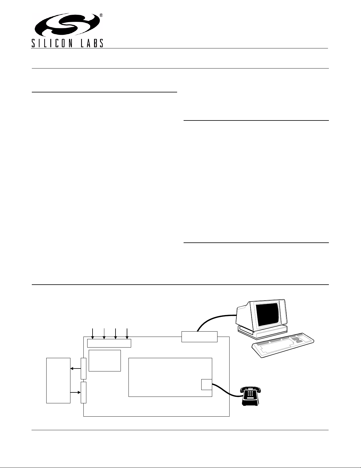
Si321xPPQx-EVB
Parallel Port
Power In
PCM TXPCM RX
Audio
Generator/
Analyzer
On-Board
PCM Clock
Generator
GND +3.3 V +5 V VIN
ProSLIC Motherboard
PC running ProSLIC LINC
software
RJ-11
Port
Si321x Daughter Card
EVALUATION BOARD FOR THE Si3210/15/16 PROSLIC
Description
This document describes the operation of the Silicon
Laboratories ProSLIC
devices supported by this document are the Si3210/15/
16 and Si3210M/15M/16M; both Si3201 and discrete
interface topologies are included. Schematics and
layouts are provided for the various ProSLIC products.
The ProSLIC evaluation platform is designed to provide
observation of the ProSLIC’s functionality. The ProSLIC
platform consists of a ProSLIC motherboard, a devicespecific daughter card, and the ProSLIC LINC™
software. The ProSLIC LINC software is a Windows
based program that can run in Microsoft Windows
environments.
Equipment requirements:
PC running Windows NT, 2000, or XP
25-pin D male-male cable
+5 V, 0.5 A power supply
+3.3 V, 0.5 A power supply (optional)
+12 V, 0.5 A power supply (Si3210, Si3215, Si3216)
Optional equipment:
Balanced audio generator and analyzer
(e.g., Audio Precision System 2 and/or HP TIMS set and/
or Wandel and Goltermann PCM-4)
®
device evaluation platform. The
8 kHz PCM signal generator and analyzer
(e.g., Audio Precision System 2 and Audio Precision SIA2322 and/or Wandel and Goltermann PCM-4)
Features
Silicon Laboratories ProSLIC device
All components necessary for linecard
implementation
Selectable secondar y pr ote ct ion
Control I/O through standard Parallel Port
®
On-board PCLK and FSYNC clock generation for
stand-alone operation
PCM I/O set up for Audio Precision System 2 or
Wandel and Goltermann PCM-4
Full access to PCM highway
Multiple daughter cards may be stacked for multi-
channel evaluation and daisy chain control
ProSLIC power selection (3.3 or 5 V)
Related Documentation
ProSLIC LINC™ User Guide
®
Functional Block Diagram
Rev. 1.2 7/08 Copyright © 2008 by Silicon Laboratories Si321xPPQx-EVB
Si321xPPQx-EVB
1. Introduction
The ProSLIC Si321x evaluation platform is a modular
system consisting of a generic motherboard and one or
more Si321x device-specific daughter cards. Using the
EVB hardware and ProSLIC LINC™ software, one can
easily configure, control, and monitor Si321x operation.
Up to eight Si321x daughter cards may be stacked
vertically and accessed using uniquely-assigned
timeslots on the common PCM interface and the SPI in
daisy-chain mode.
1.1. ProSLIC LINC evaluation software
The ProSLIC LINC software is an executable program
that allows control and monitoring of the ProSLIC. It
utilizes the primary LPT port of a standard PC to
communicate to the ProSLIC’s SPI port.
To install the software, insert the Silicon Laboratories
ProSLIC CD into the computer. The setup routine can
be invoked by running the setup.exe program in the root
directory of the CD.
Invoking the ProSLIC LINC is achieved by double
clicking the ProSLIC LINC icon. Refer to the ProSLIC
LINC User Guide for software operation.
1.2. Si321xPPT-EVB ProSLIC Evaluation Board Description
Si321x EVB daughter cards currently supported by this
hardware solution are listed in Table 1 along with
supporting hardware schematics and layout references
included in this data sheet.
Table 1. Supported Si321x EVB Daughter Cards
EVB Daughter Card Board
Description
Si3210/5/6 QFN with Si3201
integrated line interface
Si3210/5/6 QFN with discrete
line interface
Si3210/5/6M QFN with Si3201
integrated line interface
Si3210/5/6M QFN with discrete
line interface
Schematic
Figures
1, , 3 4, 5, 6
7, , 9 10, 11 , 12
13, 14, 15 16, 17, 18
19, 20, 21 22, 23, 24
Layout
Figures
Motherboard hardware schemat ics are foun d in Figures
25, 26, and 27.
All power and signal connections are made to the
motherboard as described in Table 2.
Signal requirements for ProSLIC operation are PCLK,
FS, and Serial IO. The ProSLIC motherboard has a
local oscillator with a programmable logic device to
provide the ProSLIC PCLK FS signals. The DIP switch
(S2) sets the PCLK frequency and controls the FS
enable. See Table 3 for S2 settings. Factory default
setting is for a 2.048 MHz PCLK with F5 enabled. JP3
and JP4 select this internal clock source or an exter nal
PCM clock source. The ProSLIC motherboard ha s been
designed to directly connect to an Audio Precision SIA2322 Serial Interface Adapter through the 15 pin dconnectors, P2 and P3 (not installed). See Table 5 for
the Audio Precision settings. The ProSLIC evaluation
board has also been designed to interface with a
Wandel and Goltermann PCM-4 through J8, J9, J10,
and J11 (not installed). See Table 6 for PCM-4 settings.
A header, J5 (not installed), allows access to the
ProSLIC’s PCM signals for connection to other PCM
testing devices or an actual telephone system PCM
bus. TIP and RING of the two wire analog interface is
present at the RJ-11 connector, J1.
The ProSLIC evaluation board is voltage-programmable
with specific jumper settings. JP1 selects 3 or 5 V
ProSLIC operation. JP2 selects 3 or 5 V PCM source
level compatibility. These should be placed on the
expected setting. Table 4 shows a summary of JP1–4
settings.
Power is connected to the ProSLIC at J3 and J4, and
supply connections are summarized in Table 1. The 5 V
is always required for the buffers, U2 and U3, to
interface to the parallel port. The ProSLIC can be
powered from 5 V or 3 V with the placement of a jumper
on JP1. The Protection Return connections on J6 are to
be connected to an appropriate ground for TIP/RING
fault testing. This return is tied to signal ground on
board, although it has a dedicated trace for high-current
conditions. Serial control of the ProSLIC is achieved by
toggling select bits of a standard parallel port. The
parallel port connection is available at P1 and J1.
The ProSLIC card can be daisy-chained by simply
stacking the cards. Stack up to eight cards by aligning
JS1–JS6 and pressing together. The ProSLIC LINC
Software allows channel-specific commands by clicking
the Daisy Chain button.
2 Rev. 1.2
Si321xPPQx-EVB
Table 2. Motherboard Power Connections
J2, J3, J4
Si321x Si321xM
VBRING NC NC
VBHI NC NC
VBLO NC NC
GND
GND GND
GND
+3 V +3.3 V
+5 V +5 V +5 V
+VIN +9 to 12 V
Notes:
1. All three GND connection points are electrically
connected on the board.
2. +3.3 V is only necessary if that is the desired VDD for
operation. Si321x chooses +3.3 V or +5 V based on
the SP1 of the motherboard (see schematic).
3. This may be changed based on application-specific
circuits. Consult the dc-dc converter spreadsheet for
other possible values.
1
2
3
GND
+3.3 V
+5 V
1.3. ProSLIC Evaluation Board Setup
To prepare the ProSLIC evaluation board for use,
perform the following steps:
1. Set power supplies to 3.3 V, 5 V, and 12 V.
2. With these supplies off, connect them to J3 and J4
corresponding to the silk screen designators.
3. Connect the PC’s parallel port (LPT1) to P1 (or J1)
using a 25-pin D male-to-male cable.
4. Select the on-board PCM clock source, or select an
1
2
3
external PCM source, and connect an Audio
Precision SIA-2322 to P2 and P3 or a Wandel and
Goltermann PCM-4 to J8, J9, J10, and J11.
5. TIP/RING connection can be made from the RJ-11 to
a phone or telephony test equipment.
6. Invoke the ProSLIC LINC software.
7. Turn the power supplies on and press the ProSLIC
evaluation board reset button (S1).
8. Click the “Reinitialize” button in the ProSLIC LINC
software panel
The ProSLIC is now ready to perform its linecard
function.
Table 3. On-Board PCLK Settings (S2)
S2-1,2,3 S2-4 S2-5 S2-6 S2-7 S2-8
PCLK frequency Unused Unused Unused Unused FS enable
0,0,0 = 8.192 MHz
x x x x 0 = FS disabled
0,0,1 = 4.096 MHz
0,1,0 = 2.048 MHz
0,1,1 = 1.024 MHz
1,x,x = 512 kHz
Note: 1 = on.
Table 4. JP1–4 Settings
Jumper Function
JP1
JP2
JP3
JP4
VDD Level Select
VPCM Level Select
FSYNC Level Select
PCLK Source Select
Jumper Location
1–2 2–3
+3 V +5 V 1–2
+3 V +5 V 2–3
Internal External 1–2
Internal External 1–2
1 = FS enabled
Default Factory
Setting
Rev. 1.2 3
Si321xPPQx-EVB
Table 5. Audio Precision SIA-2322 DIP Switch Setting
Receiver Mode Transmitter Mode
00111001 00000010 11111101 01111001 0000001 00000010 11111101 01111001
Note: 256 kHz PCLK and 8 kHz FS.
Table 6. Wandel and Goltermann PCM-4 Settings
General Configuration 2.14
General Configuration 3.13
General Configuration 4.13
For µ-law Add the Following:
General Configuration 7.12
General Configuration 7.22
4 Rev. 1.2
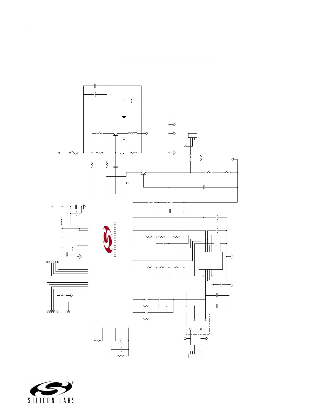
2. Schematics
FSYNC
DRX
SDO
SDI
PCLK
SCLKDTX
VBAT
/RESET
/CS
/INT
+VDC
VCC
VCC
VCC
SDITHRU
RING
TIP
/INT
SCLK
SDO
DRX
FSYNC
TIP_ext
RING_ext
PCLK
DTX
/RESET
/CS
SDI
TEST
PCM Bus Control Bus
Note 5: D1 = Central Semi CMR1U-02M or equivalent
Note 4: L1 = Delevan or Sumida SPD127 series or equivalent
see application note for value selection
Note 3: C30 to be Tantalum or Ceramic
Note 2: All capacitors are 100V, 20% unless otherwise noted
Note 1: All resistors are 1/10 W, 1% unless otherwise noted
RFILT
TIP
RING
Protection
CFILT
* These component need to be
selected appopriatedly for the
corresponding VDC voltage level.
See the data sheet and the AN45
app note for component value.
1-2: VCC=3.3V
2-3: VCC=5V
Note 4
--Single point connection
to ground plane
Over V
Note 5
Localized ground traces
ProSLIC
CTC CRC
F1
500mAF1500mA
C14
0.1uF
C14
0.1uF
L2
47 uH
150 mAL247 uH
150 mA
11223344556
6
J1
RJ-11J1RJ-11
C6
22 nFC622 nF
R17
200
R17
200
R102
90.9k
R102
90.9k
R5
100k
RBATR5100k
RBAT
Q8
2222
QBATDQ82222
QBATD
12
C15
0.1 uF
C15
0.1 uF
L1
100 uH
LSWL1100 uH
LSW
Q9
2222Q92222
C25
10 uF
C25
10 uF
Q7
FZT953
QBATQ7FZT953
QBAT
+
C18
4.7 uF+C18
4.7 uF
R105
100k
R105
100k
R1
200k
RTDC
R1
200k
RTDC
Test PointTest Point
12
C30
10 uF
10V
C30
10 uF
10V
R8
470
RTAC
R8
470
RTAC
R36 37.4kR36 37.4k
R3
200k
RRDC
R3
200k
RRDC
C31NIC31
NI
R9
470
RRAC
R9
470
RRAC
R29
665K
R29
665K
C32NIC32
NI
Tip1NC2Ring3VBAT4VBATH5NC6GND7VDD
8
NC
9
SRINGE
10
STIPE
11
NC
12
IRINGN
13
IRINGP
14
ITIPN
15
ITIPP
16
GND
epad
U2
Si3201U2Si3201
C33NIC33
NI
R4
105kR4105k
+
C19
4.7 uF+C19
4.7 uF
R28 26.1kR28 26.1k
C26
0.1uF
C26
0.1uF
R104
90.9k
R104
90.9k
D1
ES1D
DSW
D1
ES1D
DSW
R16
200
RSW
R16
200
RSW
R20
56.2k
RMONL
R20
56.2k
RMONL
12
C16
0.1 uF
C16
0.1 uF
R18
0.68
RVDC
1/4 W
R18
0.68
RVDC
1/4 W
Test PointTest Point
R19
56.2k
RMONH
R19
56.2k
RMONH
R7
4.02kR74.02k
R2115R21
15
C20
0.1 uF
C20
0.1 uF
SCLK
34
SDI
33
SDO
32
/CS
35
/INT
36
PCLK
37
DRX
38
DTX
1
FSYNC
2
/RESET
3
ITIPP
24
ITIPN
25
IRINGP
22
IRINGN
21
STIPDC
11
STIPE
13
SRINGDC
12
SRINGE
15
STIPAC
16
SRINGAC
17
CAPM10CAPP
8
IGMP20IGMN
18
SVBAT
14
IREF
7
DCDRV
30
DCFF
29
SDCL
5
VDDD
26
VDDA2
23
SDCH
4
VDDA1
6
GNDD
27
SDITHRU
31
QGND
9
GNDA
19
TEST
28
U1
Si3210-FM
U1
Si3210-FM
R14
40.2k
RREF
R14
40.2k
RREF
R15
243
RGM
R15
243
RGM
+
C1
10 uFCL10V+C1
10 uFCL10V
C3
220 nF
CTACC3220 nF
CTAC
+
C2
10 uFCM10V+C2
10 uFCM10V
C4
220 nF
CRACC4220 nF
CRAC
Test PointTest Point
R26
40.2k
R26
40.2k
Test PointTest Point
12
C17
0.1 uF
C17
0.1 uF
Test PointTest Point
11223
3
J2J2
R6
4.02kR64.02k
12
C34
10 uF
10V
C34
10 uF
10V
R2
105kR2105k
C10
0.1uF
CFF
C10
0.1uF
CFF
C9
10 uF
CBATC910 uF
CBAT
C5
22 nFC522 nF
Test PointTest Point
Si321xPPQx-EVB
Rev. 1.2 5
Figure 1. Si321x QFN with Si3201 Schematic (1 of 3)
Si321xPPQx-EVB
SDI1
/CS1_TEST
/CS0
SDI0
SDI
VCC
+VDC
/CS
SDI
TEST
SDITHRU
SCLK
DRX
FSYNC
PCLK
/RESET
SDO
DTX
/INT
(Farside)
SPI assignment:
To use /CS0, apply a zero Ohm resistor to R45 and R46
do not install R44
To use /CS1, apply a zero Ohm resistor to R44
do not install R45 and R46
To use SDI0, apply a zero Ohm resistor to R43 and R47
do not install R42 and R48
To use SDI1, apply a zero Ohm resistor to R42 and R48
do not install R43 and R47
R450R45
0
1
1
2
2
3
3
4
4
5
5
6
6
7
7
8
8
9
9
10
10
JS4
CONN SOCKET 5x2
JS4
CONN SOCKET 5x2
112
2
334
4
556
6
778
8
9910
10
JS5
CONN SOCKET 5x2
JS5
CONN SOCKET 5x2
R42NIR42
NI
R25
56.2k
R25
56.2k
R47 0R47 0
1
1
3
3
2
2
4
4
JS2
CONN SOCKET 2x2/SM
JS2
CONN SOCKET 2x2/SM
R48 NIR48 NI
1
1
2
2
3
3
4
4
5
5
6
6
7
7
8
8
9
9
10
10
JS3
CONN SOCKET 5x2
JS3
CONN SOCKET 5x2
R430R43
0
R460R46
0
1
1
3
3
2
2
4
4
JS6
CONN HDR 2x2/SM
JS6
CONN HDR 2x2/SM
R44NIR44
NI
1
1
2
2
3
3
4
4
5
5
6
6
7
7
8
8
9910
10
JS1
CONN SOCKET 5x2
JS1
CONN SOCKET 5x2
Figure 2. Si321x QFN with Si3201 Schematic (2 of 3)
6 Rev. 1.2
Si321xPPQx-EVB
TIP
TIP_ext
RING_ext
RING
GR-1089
component
GR-1089
Intra-Building
component
R41 10R41 10
c
D5
NI
P1101CA2
c
D5
NI
P1101CA2
c
D4
Thyristor-Diode
P1101SC
c
D4
Thyristor-Diode
P1101SC
1 2
RF1
F1250T
RF1
F1250T
c
D3
Thyristor-Diode
P1101SC
c
D3
Thyristor-Diode
P1101SC
R40 10R40 10
1 2
RF2
F1250T
RF2
F1250T
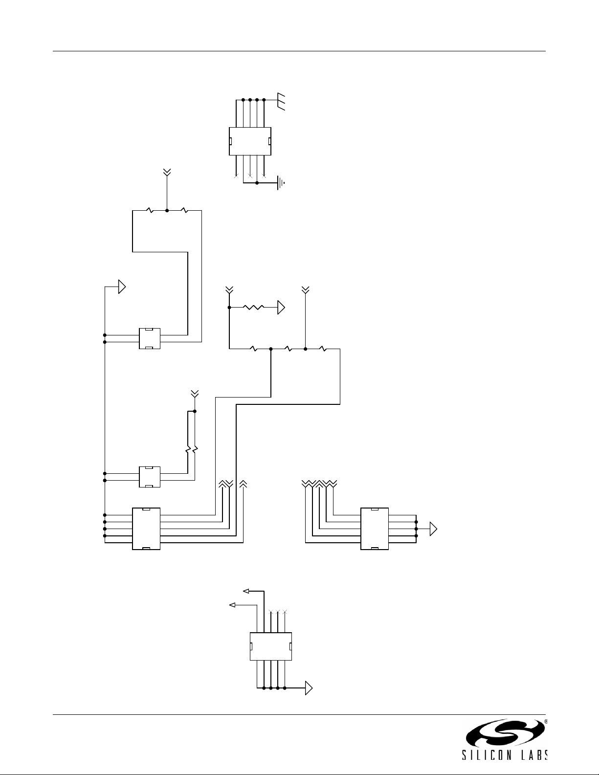
Figure 3. Si321x QFN with Si3201 Schematic (3 of 3)
Rev. 1.2 7

Si321xPPQx-EVB
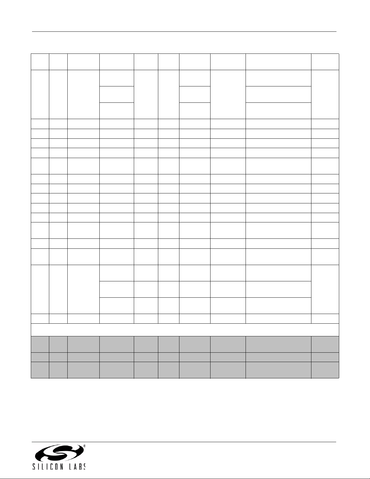
3. Si321x-FM-DC1 Bill of Materials
Table 7. Si321x-FM-DC1 Bill of Materials
Item Qty Ref Value Rating Tol Dielectric PCB
Footprint
14C1,C2,
C30,C34
2 2 C3,C4 220 nF 100 V ±20% X7R 1812 18121C224MATA AVX
3 2 C5,C6 22 nF 100 V ±20% X7R 1206 12061C223MATA AVX
4 2 C9,C25 10 µF 100 V ±20% Elec C100[6238]6
5 3 C10,C14,
C26
6 4 C15,C16,
C17,C20
7 2 C18,C19 4.7 µF 16 V ±20% X7R 1206 C1206X7R160-475MNE Venkel
10 1 D1 ES1D DO-214 ES1D Central
11 2 D3,D4 Thyristor-
12 1 F1 500 mA F1206[60X6
13 4 JS1,JS3,
JS4,JS5
14 1 JS2 SOCKET
15 1 JS6 HDR 2x2/
16 1 J1 RJ-11 RJ11-6-SMT 555077-2 AMP
17 1 J2 HEADER
18 1 L1 100 µH 1.7 A IND[220X15
19 1 L2 47 µH 150 mA IND-
20 1 Q7 FZT953 SOT-223 FZT953 Zetex
21 2 Q8,Q9 2222 SOT-23 MMBT2222 Motorola
22 2 RF1,RF2 TeleLink F350[145X1
23 2 R1,R3 200 k 1/10 W ±1% 0805 CR0805-10W-2003FT Venkel
24 2 R2,R4 105 k 1/10 W ±1% 0805 CR0805-10W-1053FT Venkel
25 2 R5,R105 100 k 1/10 W ±1% 0805 CR0805-10W-1003FT Venkel
26 2 R6,R7 4.02 k 1/10 W ±1% 0805 CR0805-10W-4021FT Venkel
10 µF 10 V ±20% X7R 1206 C1206X7R100-106MNE Venkel
.3MMR
0.1 µF 100 V ±20% X7R 1206 12061C104MATA AVX
0.1 µF 16 V ±20% X7R 0603 0603YC104MATA AVX
DO-214 P1101SC Littelfuse
Diode
0]
SOCKET
5x2
2x2/SM
SM
3X1
CONN2X5-
SSQ
CONN2X2-
100-SSM
CONN2X2-
100-TSM
CONN-1X3 2303-6111TN 3M
0]SPD
NLC3225
57]
Mfr Part Number Mfr
ECA-2AM100 Pana-
sonic
Semi
SSQ 500 Bel Fuse
Inc.
SSQ-1-05-24-F-D Samtec
SSM-102-L-DV-TR Samtec
TSM-102-02-T-DV Samtec
SPD127-104 API
Delevan
NLC322522T-470K TDK
F1250T Littelfuse
8 Rev. 1.2
Si321xPPQx-EVB
Table 7. Si321x-FM-DC1 Bill of Materials (Continued)
Item Qty Ref Value Rating Tol Dielectric PCB
Footprint
27 2 R8,R9 470
(Si3210-FM)
4.7 k
(Si3215-FM)
4.7 k
(Si3216-FM)
28 2 R14,R26 40.2 k 1/10 W ±1% 0805 CR0805-10W-4022FT Venkel
29 1 R15 243 1/10 W ±1% 0805 CR0805-10W-2430FT Venkel
30 2 R16,R17 200 1/10 W ±5% 0805 CR0805-10W-201JT Venkel
31 1 R18 0.68 1/4 W ±5% 1206 CR1206-4W-R68JT Venkel
32 3 R19,R20,
R25
33 1 R21 15 1/10 W ±1% 0805 CR0805-10W-15R0FT Venkel
34 1 R28 26.1 k 1/10 W ±1% 0805 CR0805-10W-2612FT Venkel
35 1 R29 665 k 1/10 W ±1% 0805 CR0805-10W-6653FT Venkel
36 1 R36 37.4 k 1/10 W ±1% 0805 CR0805-10W-3742FT Venkel
37 2 R40,R41 10 1/10 W ±1% 0805 CR0805-10W-10R0FT Venkel
38 4 R43,R45,
R46,R47
39 2 R102,R104 90.9 k 1/10 W ±1% 0805 CR0805-10W-9092FT Venkel
40 3 GND, TIP,
RING
41 1 U1 Si3210-FM MLF38N5X7
42 1 U2 Si3201 SOIC16 Si3201-FS Rev E Silabs
56.2 k 1/10 W ±1% 0805 CR0805-10W-5622FT Venkel
0 1/10 W ±1% 0805 CR0805-10W-0000FT Venkel
Test Point 151-205 Mouser
Si3215-FM MLF38N5X7
Si3216-FM MLF38N5X7
1/10 W ±1% 0805 CR0805-10W-4700FT Venkel
CR0805-10W-4701FT
CR0805-10W-4701FT
-0.5P
-0.5P
-0.5P
Mfr Part Number Mfr
Si3210-FM Rev E Silabs
Si3215-FM Rev C
Si3216-FM Rev C
Not Installed Components
43 3 C31,C32,
C33
44 1 D5 P1101CA2 95 V DO-214AA-3 P1101CA2 Te ccor
45 3 R42,R44,
R48
Rev. 1.2 9
Si321xPPQx-EVB
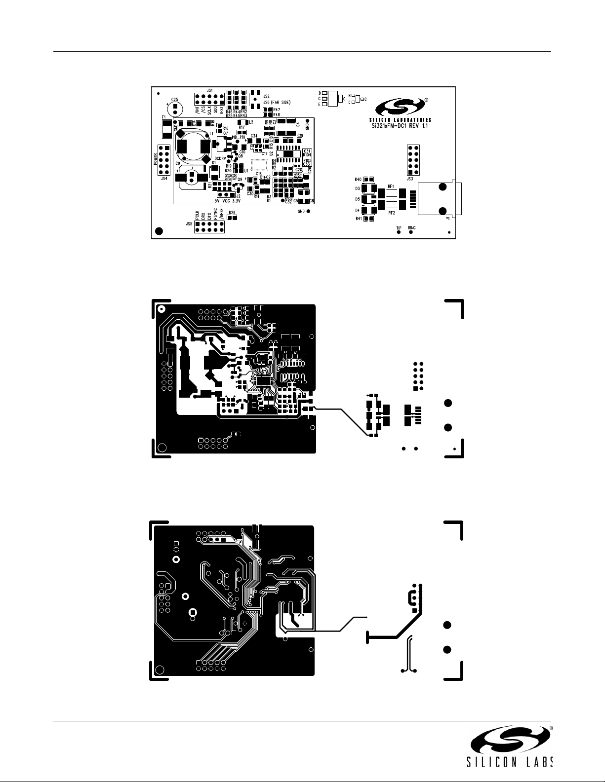
Figure 4. Si321xFM-DC1-EVB with Si3201 Primary Assembly
Figure 5. Si321xFM-DC1-EVB with Si3201 Primary Side
Figure 6. Si321xFM-DC1-EVB with Si3201 Secondary Side
10 Rev. 1.2

/RESET
TEST
/INT
SDO
SCLK
SDI
/CS
PCLK
DRX
DTX
FSYNC
SDITHRU
VBAT
+VDC
VCC
VCC
/CS
SDO
SDI
SCLK
/INT
SDITHRU
TIP
RING
TEST
DRX
DTX
FSYNC
/RESET
PCLK
TIP_EXT
RING_EXT
PCM Bus
Control Bus
Note 5: D1 = Central Semi CMR1U-02M or equivalent
Note 4: L1 = Delevan or Sumida SPD127 series or equivalent
see application note for value selection
Note 3: C30 to be Tantalum or Ceramic
Note 2: All capacitors are 100V, 20% unless otherwise noted
Note 1: All resistors are 1/10 W, 1% unless otherwise noted
TIP
RING
Protection
CFILT
1-2: VCC=3.3V
2-3: VCC=5V
Note 4
--Single point connection
to ground plane
Over V
Note 5
Localized ground traces
* These component need to be
selected appopriatedly for the
corresponding VDC voltage level.
See the data sheet and the AN45
app note for component value.
RFILT
R29
665K
R29
665K
C33
0.1 uF
C33
0.1 uF
C25
10 uF
C25
10 uF
Q5
CZT5551
QRPQ5CZT5551
QRP
12345
6
J1
RJ-11J1RJ-11
Q6
CZT5551
QTNQ6CZT5551
QTN
L1
100 uHL1100 uH
R102
100k
R102
100k
R18
0.68
1/4 W
R18
0.68
1/4 W
Q1
CMPT5401
QTPQ1CMPT5401
QTP
Test PointTest Point
C26
0.1uF
C26
0.1uF
12
C15
0.1 uF
C15
0.1 uF
Q3
CMPT5401
QRDNQ3CMPT5401
QRDN
R4
100k
RRSE45
R4
100k
RRSE45
Q2
CMPT5401
QRNQ2CMPT5401
QRN
Q4
CMPT5401
QTDNQ4CMPT5401
QTDN
Q9
MMBT2222Q9MMBT2222
12
C30
10 uF
10V
C30
10 uF
10V
Test PointTest Point
Test PointTest Point
R1
200k
RTDC
R1
200k
RTDC
R8
470
RTAC
R8
470
RTAC
R3
200k
RRDC
R3
200k
RRDC
R19 56.2kR19 56.2k
R9
470
RRAC
R9
470
RRAC
Test PointTest Point
R1010RTBP
R1010RTBP
R104
100k
R104
100k
Test PointTest Point
R5
100k
RBATR5100k
RBAT
R7
80.6
RRER780.6
RRE
Q8
MMBT2222Q8MMBT2222
R12
5.1k
RRBN
R12
5.1k
RRBN
C32
0.1 uF
C32
0.1 uF
R2115R21
15
R6
80.6
RTER680.6
RTE
R23
3.0k
RRBN0
R23
3.0k
RRBN0
R13
5.1k
RTBN
R13
5.1k
RTBN
12
C16
0.1 uF
C16
0.1 uF
R1110RRBP
R1110RRBP
C10 0.1uFC10 0.1uF
R28 26.1kR28 26.1k
11223
3
J2J2
R105
100k
R105
100k
Q7
FZT953Q7FZT953
R17
200
R17
200
R14
40.2k
RREF
R14
40.2k
RREF
R26
56.2k
R26
56.2k
R15
243
RGM
R15
243
RGM
C1
10 uFCLC1
10 uF
CL
C3
220 nF
CTAC
C3
220 nF
CTAC
C2
10 uFCMC2
10 uF
CM
C31
0.1 uF
C31
0.1 uF
C9
10 uFC910 uF
12
C17
0.1 uF
C17
0.1 uF
C4
220 nF
CRAC
C4
220 nF
CRAC
Test PointTest Point
C5
22 nF
CTCC522 nF
CTC
C6
22 nF
CRCC622 nF
CRC
D1
ES1DD1ES1D
12
C34
10 uF
10V
C34
10 uF
10V
R16
200
R16
200
C8
0.1uF
CTBNC80.1uF
CTBN
C7
0.1uF
CRBNC70.1uF
CRBN
C14
0.1uF
C14
0.1uF
SCLK
34
SDI
33
SDO
32
/CS
35
/INT
36
PCLK
37
DRX
38
DTX
1
FSYNC
2
/RESET
3
ITIPP
24
ITIPN
25
IRINGP
22
IRINGN
21
STIPDC
11
STIPE
13
SRINGDC
12
SRINGE
15
STIPAC
16
SRINGAC
17
CAPM10CAPP
8
IGMP20IGMN
18
SVBAT
14
IREF
7
DCDRV
30
DCFF
29
SDCL
5
VDDD
26
VDDA2
23
SDCH
4
VDDA1
6
GNDD
27
SDITHRU
31
QGND
9
GNDA
19
TEST
28
U1
Si3210-FM
ProSLIC
U1
Si3210-FM
ProSLIC
R2
100k
RTSE
R2
100k
RTSE
F1
500mAF1500mA
R36 37.4kR36 37.4k
R24
3.0k
RTBN0
R24
3.0k
RTBN0
R20 56.2kR20 56.2k
L2
47 uH
150 mAL247 uH
150 mA
Si321xPPQx-EVB
Rev. 1.2 11
Figure 7. Si321x QFN with Discrete Evaluation Circuit (1 of 3)
Si321xPPQx-EVB
/CS1_TEST
/CS0
SDI0
SDI
SDI1
+VDC
VCC
/CS
SDI
DRX
PCLK
TEST
FSYNC
/RESET
SCLK
SDITHRU
SDO
/INT
DTX
(Farside)
Chain 0
Chain 1
Chain 0
Chain 1
SPI assignment:
To use /CS0, apply a zero Ohm resistor to R45 and R46
do not install R44
To use /CS1, apply a zero Ohm resistor to R44
do not install R45 and R46
To use SDI0, apply a zero Ohm resistor to R43 and R47
do not install R42 and R48
To use SDI1, apply a zero Ohm resistor to R42 and R48
do not install R43 and R47
1
1
2
2
3
3
4
4
5
5
6
6
7
7
8
8
9
9
10
10
JS3
CONN SOCKET 5x2
JS3
CONN SOCKET 5x2
R44NIR44
NI
R430R43
0
1
1
3
3
2
2
4
4
JS6
CONN HDR 2x2/SM
JS6
CONN HDR 2x2/SM
R450R45
0
R47 0R47 0 R42
NI
R42
NI
R25
56.2k
R25
56.2k
R48 NIR48 NI
1
1
3
3
2
2
4
4
JS2
CONN SOCKET 2x2/SM
JS2
CONN SOCKET 2x2/SM
R460R46
0
1
1
2
2
3
3
4
4
5
5
6
6
7
7
8
8
9910
10
JS1
CONN SOCKET 5x2
JS1
CONN SOCKET 5x2
1
1
2
2
3
3
4
4
5
5
6
6
7
7
8
8
9
9
10
10
JS4
CONN SOCKET 5x2
JS4
CONN SOCKET 5x2
112
2
334
4
556
6
778
8
9910
10
JS5
CONN SOCKET 5x2
JS5
CONN SOCKET 5x2
Figure 8. Si321x QFN with Discrete Evaluation Circuit (2 of 3)
12 Rev. 1.2

Si321xPPQx-EVB
TIP
TIP_ext
RING_ext
RING
GR-1089
component
GR-1089
Intra-Building
component
1 2
RF1
F1250T
RF1
F1250T
1 2
RF2
F1250T
RF2
F1250T
c
D4
Thyristor-Diode
P1101SC
c
D4
Thyristor-Diode
P1101SC
c
D5
NI
P1101CA2
c
D5
NI
P1101CA2
c
D3
Thyristor-Diode
P1101SC
c
D3
Thyristor-Diode
P1101SC
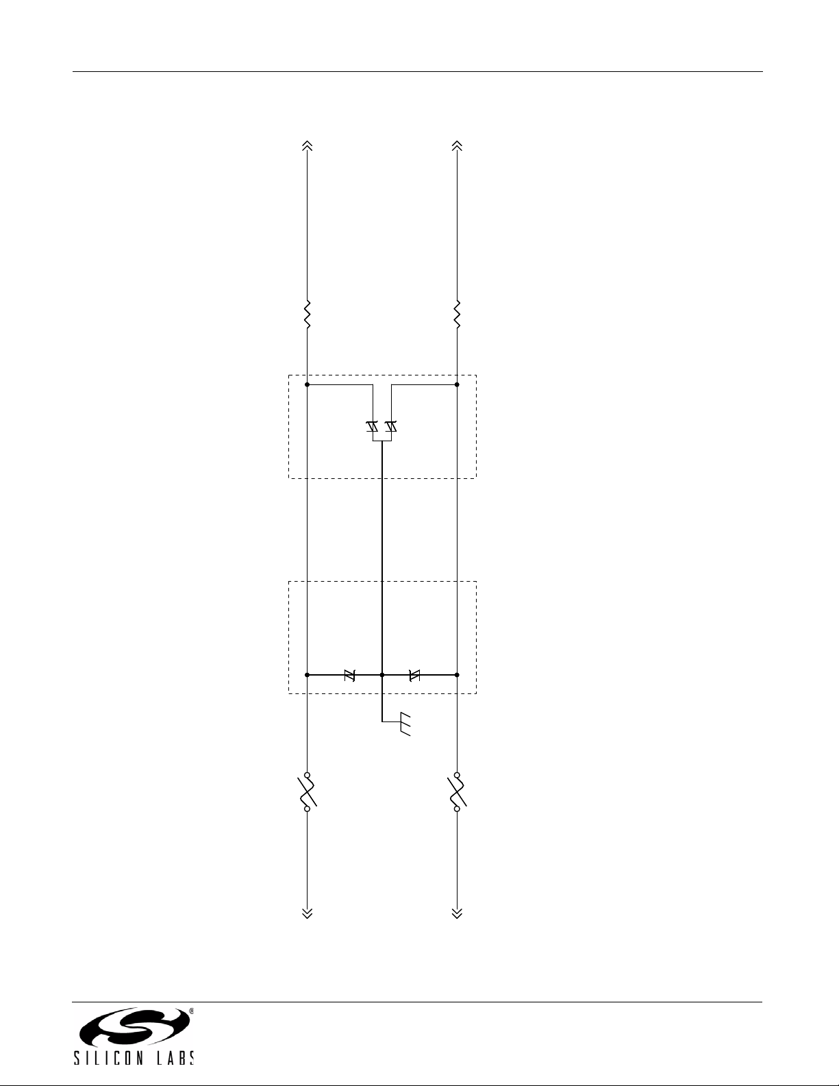
Figure 9. Si321x QFN with Discrete Evaluation Circuit (3 of 3)
Rev. 1.2 13

Si321xPPQx-EVB
4. Si321x-FM-DCX Bill of Materials
Table 8. Si321x-FM-DCX Bill of Materials
Item Qty Ref Value Rating Tol Dielectric PCB
Footprint
14C1,C2,
C30,C34
2 2 C3,C4 220 nF 100 V ±20% X7R CC1812 C1210X7R101-
3 2 C5,C6 22 nF 100 V ±20% X7R CC1206 12061C223MATA AVX
4 5 C7,C8,C10,
C14,C26
5 2 C9,C25 10 µF 100 V ±20% Elec C100[6238]
6 3 C15,C16,
C17
7 3 C31,C32,
C33
8 1 D1 ES1D DO-214AA-
9 2 D3,D4 Thyristor-
10 1 F1 500 mA F2410-SSQ SSQ 500 Bel Fuse
11 4 JS1,JS3,
JS4,JS5
12 1 JS2 CONN2X2-
13 1 JS6 CONN2X2-
14 1 J1 RJ-11 RJ11-6-SMT 555077-2 AMP
15 1 J2 HEADER
16 1 L1 100 µH 1.7 A IND[220X15
17 1 L2 47 µH 150 mA IND-
18 4 Q1,Q2,
Q3,Q4
19 2 Q5,Q6 CZT5551 SOT-223 CZT5551 Central
20 1 Q7 FZT953 SOT-223 FZT953 Zetex
21 2 Q8,Q9 MMBT2222 SOT-23 MMBT2222 On Semi
22 2 RF1,RF2 F1250T F350
23 2 R1,R3 200 k 1/10 W ±1% RC0805 CR0805-10W-2003FT Venkel
10 µF 10 V ±20% X7R CC1206 C1206X7R100-106MNE Venkel
0.1 µF 100 V ±20% X7R CC1206 12061C104MATA AVX
6.3MMR
0.1 µF 16 V ±20% X7R CC0603 0603YC104MAT A AVX
0.1 µF 50 V ±20% X7R CC0805 C0805X7R500-
REV
DO-214AA-
Diode
CONN2X5-
CONN-1X3 2303-6111TN 3M
3X1
CMPT5401 SOT-23 CMPT5401 Central
REV
SSQ
100-SSM
100-TSM
0]SPD
NLC3225
[145X157]
Mfr Part Number Mfr
Venkel
224MNER
ECA-2AM100 Pana-
sonic
Venkel
104MNER
ES1D Central
Semi
P1 101SC Littelfuse
Inc.
SSQ-1-05-24-F-D Samtec
TSM-102-02-T-DV Samtec
SSM-102-L-DV-TR Samtec
SPD127-104 API
Delevan
NLC322522T-470K TDK
Semi
Semi
F1250T Littelfuse
14 Rev. 1.2

Si321xPPQx-EVB
Table 8. Si321x-FM-DCX Bill of Materials (Continued)
Item Qty Ref Value Rating Tol Dielectric PCB
Footprint
24 6 R2,R4,R5,
R102,
R104,R105
25 2 R6,R7 80.6 1/4 W ±1% RC1210 CR1210-4W-80R6FT Venkel
26 2 R8,R9 470
27 2 R10,R11 10 1/10 W ±5% RC0805 CR0805-10W-100JT Venkel
28 2 R12,R13 5.1 k 1/10 W ±5% RC0805 CR0805-10W-512JT Venkel
29 1 R14 40.2 k 1/10 W ±1% RC0805 CR0805-10W-4022FT Venkel
30 1 R15 243 1/10 W ±1% RC0805 CR0805-10W-2430FT Venkel
31 2 R16,R17 200 1/10 W ±5% RC0805 CR0805-10W-201JT Venkel
32 1 R18 0.68 1/4 W ±5% RC1206 CR1206-4W-R68JT Venkel
33 4 R19,R20,
R25,R26
34 1 R21 15 1/10 W ±1% RC0805 CR0805-10W-15R0FT Venkel
35 2 R23,R24 3.0 k 1/10 W ±5% RC0805 CR0805-10W-302JT Venkel
36 1 R28 26.1 k 1/10 W ±1% RC0805 CR0805-10W-2612FT Venkel
37 1 R29 665 k 1/10 W ±1% RC0805 CR0805-10W-6653FT Venkel
38 1 R36 37.4 k 1/10 W ±1% RC0805 CR0805-10W3742FT Venkel
39 4 R43,R45,
R46,R47
40 3 GND, TIP,
RING
41 1 U1 Si3210-FM MLF38N
Not Installed Compo ne nts
41 1 D5 NI 95 V DO-214AA-3 P1101CA2 Teccor
42 3 R42,R44,
R48
100 k 1/10 W ±1% RC0805 CR0805-10W-1003FT Venkel
1/10 W ±1% RC0805 CR0805-10W-4700FT Venkel
(Si3210-FM)
4.7 k
(Si3215-FM)
4.7 k
(Si3216-FM)
56.2 k 1/10 W ±1% RC0805 CR0805-10W-5622FT Venkel
0 1/16 W ±1% RC0805 CR0805-16W-0000FT Venkel
Test Point 151-205 Mouser
Si3215-FM Si3215-FM Rev C
Si3216-FM Si3216-FM Rev C
NI
5X7-0.5P
Mfr Part Number Mfr
CR0805-10W-4701FT
CR0805-10W-4701FT
Si3210-FM Rev E Silabs
Rev. 1.2 15

Si321xPPQx-EVB
Figure 10. Si321xFM-DCX-EVB with Discretes Primary Assembly
Figure 11. Si321xFM-DCX-EVB with Discretes Primary Side
Figure 12. Si321xFM-DCX-EVB with Discretes Secondary Side
16 Rev. 1.2

FSYNC
TEST
DRX
PCLK
/RESET
DTX
/CS
/INT
SDI
SCLK
SDO
VCC
+VDC
VCC
VCC
DRX
FSYNC
TIP_ext
RING_ext
RING
TEST
TIP
/INT
/CS
PCLK
DTX
/RESET
SDI
SCLK
SDO
SDITHRU
PCM Bus Control Bus
Note 5: D1 = Central Semi CMR1U-02M or equivalent
Note 4: L1 = Delevan or Sumida SPD127 series or equivalent
see application note for value selection
Note 3: C30 to be Tantalum or Ceramic
Note 2: All capacitors are 100V, 20% unless otherwise noted
Note 1: All resistors are 1/10 W, 1% unless otherwise noted
RFILT
Localized ground traces
--Single point connection
to ground plane
TIP
RING
Protection
CFILT
1-2: VCC=3.3V
2-3: VCC=5V
Over V
* These component need to be selected appopriatedly for
the corresponding VDC voltage level. See the data sheet
the and AN45 app note for component value.
ProSLIC
11223344556
6
J1
RJ-11J1RJ-11
12
C15
0.1 uF
C15
0.1 uF
R4
105kR4105k
1 2
C5
22 nF
CTCC522 nF
CTC
R20
16.5k
RMONL
R20
16.5k
RMONL
12
C18
4.7 uF
C18
4.7 uF
R19
16.5k
RMONH
R19
16.5k
RMONH
12
C20
0.1 uF
C20
0.1 uF
R105
100k
R105
100k
12
C30
10 uF
C30
10 uF
C32NIC32
NI
R1
200k
RTDC
R1
200k
RTDC
Test PointTest Point
Test PointTest Point
SCLK
34
SDI
33
SDO
32
/CS
35
/INT
36
PCLK
37
DRX
38
DTX
1
FSYNC
2
/RESET
3
ITIPP
24
ITIPN
25
IRINGP
22
IRINGN
21
STIPDC
11
STIPE
13
SRINGDC
12
SRINGE
15
STIPAC
16
SRINGAC
17
CAPM10CAPP
8
IGMP20IGMN
18
SVBAT
14
IREF
7
DCDRV
30
DCFF
29
SDCL
5
VDDD
26
VDDA2
23
SDCH
4
VDDA1
6
GNDD
27
SDITHRU
31
QGND
9
GNDA
19
TEST
28
U1
Si3210M-FM
U1
Si3210M-FM
R8
470
RTAC
R8
470
RTAC
R36 37.4kR36 37.4k
1 2
C9
10 uF
CBAT0C910 uF
CBAT0
R3
200k
RRDC
R3
200k
RRDC
Test PointTest Point
R29
665K
R29
665K
R9
470
RRAC
R9
470
RRAC
1 2
C27
470pF
C27
470pF
Q9
MMBT2222Q9MMBT2222
R32 0R32 0
R7
4.02kR74.02k
C31NIC31
NI
R33 NIR33 NI
12
C19
4.7 uF
C19
4.7 uF
Tip1NC2Ring3VBAT4VBATH5NC6GND7VDD
8
NC
9
SRINGE
10
STIPE
11
NC
12
IRINGN
13
IRINGP
14
ITIPN
15
ITIPP
16
GND
epad
U2
Si3201U2Si3201
R2115R21
15
R6
4.02kR64.02k
R5
100k
RBATR5100k
RBAT
12
C16
0.1 uF
C16
0.1 uF
R34 NIR34 NI
R28 26.1kR28 26.1k
D1
CMR1U-02M
DSW
D1
CMR1U-02M
DSW
12
C26
0.1 uF
C26
0.1 uF
F1
FuseF1Fuse
R26
40.2k
R26
40.2k
C14
0.1 uF
C14
0.1 uF
12
C34
10 uF
C34
10 uF
R18
0.1
RVDC
R18
0.1
RVDC
M1
IRLL014NM1IRLL014N
R102
90.9k
R102
90.9k
R14
40.2k
RREF
R14
40.2k
RREF
1 2
C6
22 nF
CRCC622 nF
CRC
12
C17
0.1 uF
C17
0.1 uF
R22 15R22 15
R15
243
RGM
R15
243
RGM
12
C1
10 uFCLC1
10 uF
CL
12
C3
220 nF
CTAC
C3
220 nF
CTAC
12
C2
10 uFCMC2
10 uF
CM
12
C4
220 nF
CRAC
C4
220 nF
CRAC
C33NIC33
NI
R104
90.9k
R104
90.9k
2 6101
4
3 8
Transformer
T1
Transformer
T1
11223
3
J2J2
R2
105kR2105k
12
C25
10 uF
C25
10 uF
L2
47 uH
150 mAL247 uH
150 mA
R23
200k
R23
200k
Test PointTest Point
Si321xPPQx-EVB
Rev. 1.2 17
Figure 13. Si321xM QFN with Si3201 Schematic (1 of 3)

Si321xPPQx-EVB
SDI1
/CS1_TEST
/CS0
SDI0
SDI
VCC
+VDC
/CS
SDI
TEST
SDITHRU
SCLK
DRX
FSYNC
PCLK
/RESET
SDO
DTX
/INT
(Farside)
SPI assignment:
To use /CS0, apply a zero Ohm resistor to R45 and R46
do not install R44
To use /CS1, apply a zero Ohm resistor to R44
do not install R45 and R46
To use SDI0, apply a zero Ohm resistor to R43 and R47
do not install R42 and R48
To use SDI1, apply a zero Ohm resistor to R42 and R48
do not install R43 and R47
1
1
2
2
3
3
4
4
5
5
6
6
7
7
8
8
9
9
10
10
JS4
CONN SOCKET 5x2
JS4
CONN SOCKET 5x2
R460R46
0
1
1
3
3
2
2
4
4
JS2
CONN SOCKET 2x2/SM
JS2
CONN SOCKET 2x2/SM
R44NIR44
NI
R48 NIR48 NI
112
2
334
4
556
6
778
8
9910
10
JS5
CONN SOCKET 5x2
JS5
CONN SOCKET 5x2
1
1
2
2
3
3
4
4
5
5
6
6
7
7
8
8
9910
10
JS1
CONN SOCKET 5x2
JS1
CONN SOCKET 5x2
R42NIR42
NI
1
1
2
2
3
3
4
4
5
5
6
6
7
7
8
8
9
9
10
10
JS3
CONN SOCKET 5x2
JS3
CONN SOCKET 5x2
R25
56.2k
R25
56.2k
R430R43
0
R450R45
0
R47 0R47 0
1
1
3
3
2
2
4
4
JS6
CONN HDR 2x2/SM
JS6
CONN HDR 2x2/SM
Figure 14. Si321xM QFN with Si3201 Schematic (2 of 3)
18 Rev. 1.2

Si321xPPQx-EVB
TIP
TIP_ext
RING_ext
RING
GR-1089
component
GR-1089
Intra-Building
component
1 2
RF1
F1250T
RF1
F1250T
c
D3
Thyristor-Diode
P1101SC
c
D3
Thyristor-Diode
P1101SC
R40 10R40 10
R41 10R41 10
1 2
RF2
F1250T
RF2
F1250T
c
D5
NI
P1101CA2
c
D5
NI
P1101CA2
c
D4
Thyristor-Diode
P1101SC
c
D4
Thyristor-Diode
P1101SC
Figure 15. Si321xM QFN with Si3201 Schematic (3 of 3)
Rev. 1.2 19

Si321xPPQx-EVB
5. Si321xM-FM-DC1 Bill of Materials
Table 9. Si321xM-FM-DC1 Bill of Materials
Item Qty Ref Value Rating Tol Dielectric PCB Footprint Mfr Part Number Mfr
14C1,C2,
C30,C34
2 2 C3,C4 220 nF 100 V ±20% X7R CC1812 C1210X7R101-
3 2 C5,C6 22 nF 100 V ±20% X7R CC1206 12061C223MATA AVX
4 2 C9,C25 10 µF 100 V ±20% Elec C2.5X6.3MM-
5 2 C14,C26 0.1 µF 100 V ±20% X7R CC1206 12061C104MATA AVX
6 4 C15,C16,
C17,C20
7 2 C18,C19 4.7 µF 16 V ±20% X7R 1206 C1206X7R160-475MNE Venkel
8 1 C27 470 pF 100 V ±20% X7R CC1206 12061C470MATA AVX
9 1 D1 CMR1U-02M DO-214AA-REV CMR1U-02M Central
10 2 D3,D4 Thyristor-
11 1 F1 Fuse 0.5 A F1206[60X60] R451.500 Littelfuse
12 4 JS1,JS3,
JS4,JS5
13 1 JS2 CONN2X2-100-
14 1 JS6 CONN2X2-100-
15 1 J1 RJ-11 RJ11-6-SMT 555077-2 AMP
16 1 J2 HEADER
17 1 L2 47 µH 150 mA IND-NLC3225 NLC322522T-470K TDK
18 1 M1 IRLL014N SOT-223 IRLL014N Intl Rec-
19 1 Q9 MMBT2222 SOT-23 MMBT2222 Motorola
20 2 RF1,RF2 TeleLink F350[145X157] F1250T Littelfuse
21 3 R1,R3,
R23
22 2 R2,R4 105 k 1/10 W ±1% RC0805 CR0805-10W-1053FT Venkel
23 2 R5,R105 100 k 1/10 W ±1% RC0805 CR0805-10W-1003FT Venkel
24 2 R6,R7 4.02 k 1/10 W ±1% RC0805 CR0805-10W-4021FT Venkel
10 µF 10 V ±20% X7R CC1206 C1206X7R100-106MNE Venkel
Venkel
224MNER
ECA-2AM100 Pana-
RAD
0.1 µF 16 V ±20% X7R CC0603 0603YC104MATA AVX
DO-214AA-REV P1101SC Littelfuse
Diode
CONN2X5-SSQ SSQ-1-05-24-F-D Samtec
SSM-102-L-DV-TR Samtec
SSM
TSM-102-02-T-DV Samtec
TSM
CONN-1X3 2303-6111TN 3M
3X1
200 k 1/10 W ±1% RC0805 CR0805-10W-2003FT Venkel
sonic
Semi
tifier
20 Rev. 1.2

Si321xPPQx-EVB
Table 9. Si321xM-FM-DC1 Bill of Materials (Continued)
Item Qty Ref Value Rating Tol Dielectric PCB Footprint Mfr Part Number Mfr
25 2 R8,R9 475
(Si3210M)
4.7 k
(Si3215M)
4.7 k
(Si3216M)
26 2 R14,R26 40.2 k 1/10 W ±1% RC0805 CR0805-10W-4022FT Venkel
27 1 R15 243 1/10 W ±1% RC0805 CR0805-10W-2430FT Venkel
28 1 R18 0.1 1/4 W ±1% CC1206 CR1206-4W-R100FT Venkel
29 2 R19,R20 16.5 k 1/10 W ±1% RC0805 CR0805-10W-1652FT Venkel
30 2 R21,R22 15 1/10 W ±5% RC0805 CR0805-10W-150JT Venkel
31 1 R28 26.1 k 1/10 W ±1% RC0805 CR0805-10W-2612FT Venkel
32 1 R29 665 k 1/10 W ±1% RC0805 CR0805-10W-6653FT Venkel
33 1 R32 0 1/10 W ±5% RC0805 CR0805-10W-000JT Venkel
34 1 R36 37.4 k 1/10 W ±1% RC0805 CR0805-10W-3742FT Venkel
35 2 R40,R41 10 1/10 W ±1% RC0805 CR0805-10W-10R0FT Venkel
36 4 R43,R45,
R46,R47
37 2 R102,
R104
38 3 TIP,
RING,
GND
39 1 T1 Transformer XFMR-CTX01-
40 1 U1 Si3210M-FM MLF38N5X7-0.5P Si3210M-FM Rev E Silabs
41 1 U2 Si3201 SO16E Si3201-FS Rev E Silabs
0 1/10 W ±5% RC0805 CR0805-10W-000JT Venkel
90.9 k 1/10 W ±1% RC0805 CR0805-10W-9092FT Venkel
Test Point 151-20 5 Mouser
Si3215M-FM MLF38N5X7-0.5P Si3215M-FM Rev C
Si3216M-FM MLF38N5X7-0.5P Si3216M-FM Rev C
1/10 W ±1% RC0805 CR0805-10W-4750FT Venkel
CR0805-10W-4701FT
CR0805-10W-4701FT
31353R-02 Midcom
15275
Not Installed Components
42 NI C31,C32,
C33
43 NI D5 NI 95 V DO-214AA-3 P1101CA2 Littelfuse
44 NI R33,R34,
R42,R44,
R48
NI CC0805
NI RC0805
Rev. 1.2 21

Si321xPPQx-EVB
Figure 16. Si321xM-FM-DC1-EVB with Si3201 Primary Assembly
Figure 17. Si321xM-FM-DC1-EVB with Si3201 Primary Side
Figure 18. Si321xM-FM-DC1-EVB with Si3201 Secondary Side
22 Rev. 1.2

/INT
SDO
SCLK
SDI
/CS
PCLK
DRX
DTX
FSYNC
SDITHRU/RESET
+VDC
VCC
VCC
/CS
SDO
SDI
SCLK
/INT
SDITHRU
TIP
RING
DRX
DTX
FSYNC
/RESET
PCLK
RING_ext
TIP_ext
TEST
PCM Bus Control Bus
CFILT
International Rectifier
Note 1
Note 2: Transformer Connection:
Vdc = 3v to 9v: connect M1 to terminal 2
Vdc = 10v to 15v: connect M1 to terminal 3
Vdc = 16v to 39v: connect M1 to terminal 4
Note 1: M1 Mosfet Selection:
Vdc=3v to 15v: Use Int. Rec. IRLL014N or Intersil HUF7607D3S
Vdc=3v to 35v: Use Intersil HUF76609D3S or STMicroelectronic STD5NE10L or STN2NE10L.
Note 2
RFILT
* See data sheet and the app. note AN45 for
information about selecting component values
for the R18, R19, R20 resistors
Protection
RING
Localized ground traces
--Single point connection
to ground plane
Over V
1-2: VCC=3.3V
2-3: VCC=5V
Note 2
C1
10 uF
CL
C1
10 uF
CL
12
C16
0.1 uF
C16
0.1 uF
C14
0.1 uF
C14
0.1 uF
R7
80.6
RRE
R7
80.6
RRE
Q9
MMBT2222Q9MMBT2222
R9
470
RRAC
R9
470
RRAC
C25
10 uF
C25
10 uF
C32
0.1 uF
C32
0.1 uF
1 2
R34 NIR34 NI
12
C15
0.1 uF
C15
0.1 uF
R4
100k
RRSE45
R4
100k
RRSE45
C7
0.1 uF
CRBNC70.1 uF
CRBN
Q1
CMPT5401
QTPQ1CMPT5401
QTP
1 2
R36
37.4k
R36
37.4k
R11
10
RRBP
R11
10
RRBP
R17
200k
R17
200k
12
R29
665K
R29
665K
Q5
CZT5551
QRPQ5CZT5551
QRP
R12
5.1k
RRBN
R12
5.1k
RRBN
R102
100k
R102
100k
R14
40.2k
RREF
R14
40.2k
RREF
11223344556
6
J1
RJ-11J1RJ-11
R10
10
RTBP
R10
10
RTBP
R1
200k
RTDC
R1
200k
RTDC
R18
RVDC
R18
RVDC
R24
3.0K
RRBN4447
R24
3.0K
RRBN4447
12
C30
10 uF
10V
C30
10 uF
10V
SCLK
34
SDI
33
SDO
32
/CS
35
/INT
36
PCLK
37
DRX
38
DTX
1
FSYNC
2
/RESET
3
ITIPP
24
ITIPN
25
IRINGP
22
IRINGN
21
STIPDC
11
STIPE
13
SRINGDC
12
SRINGE
15
STIPAC
16
SRINGAC
17
CAPM
10
CAPP
8
IGMP20IGMN
18
SVBAT
14
IREF
7
DCDRV
30
DCFF
29
SDCL
5
VDDD
26
VDDA2
23
SDCH
4
VDDA1
6
GNDD
27
SDITHRU
31
QGND
9
GNDA
19
TEST
28
U1
Si3210M-FM
ProSLIC
U1
Si3210M-FM
ProSLIC
C33
0.1 uF
C33
0.1 uF
12
C17
0.1 uF
C17
0.1 uF
Q3
CMPT5401
QRDNQ3CMPT5401
QRDN
M1
IRLL014NM1IRLL014N
C5
22 nF
CTC
C5
22 nF
CTC
C3
220 nF
CTAC
C3
220 nF
CTAC
C26
0.1 uF
C26
0.1 uF
C31
0.1 uF
C31
0.1 uF
2
6
10
1
4
3
Transformer
T1
Transformer
T1
R105
100k
R105
100k
R8
470
RTAC
R8
470
RTAC
R19
RMONH
R19
RMONH
C9
10 uF
CBATC910 uF
CBAT
R23
3.0K
RRBN44
R23
3.0K
RRBN44
Q2
CMPT5401
QRNQ2CMPT5401
QRN
R104
100k
R104
100k
D1
ES1D
DSW
D1
ES1D
DSW
1 2
R32 0R32 0
C6
22 nF
CRC
C6
22 nF
CRC
Q6
CZT5551
QTNQ6CZT5551
QTN
R6
80.6
RTE
R6
80.6
RTE
1 2
R28
26.1k
R28
26.1k
C2
10 uF
CM
C2
10 uF
CM
12
C34
10 uF
10V
C34
10 uF
10V
R15
243
RGM
R15
243
RGM
F1
FUSE/SMF1FUSE/SM
R5
100k
RBAT45R5100k
RBAT45
11223
3
J2J2
R2115R21
15
C27
470pF
C27
470pF
L2
47 uH
150 mAL247 uH
150 mA
R3
200k
RRDC
R3
200k
RRDC
Q4
CMPT5401
QTDNQ4CMPT5401
QTDN
R20
RMONL
R20
RMONL
1 2
R33 NIR33 NI
C8
0.1 uF
CTBNC80.1 uF
CTBN
R2
100k
RTSE44
R2
100k
RTSE44
R2222R22
22
R13
5.1k
RTBN
R13
5.1k
RTBN
R26
47k
R26
47k
C4
220 nF
CRAC
C4
220 nF
CRAC
Si321xPPQx-EVB
Rev. 1.2 23
Figure 19. Si321xM QFN with Discrete Evaluation Circuit (1 of 3)

Si321xPPQx-EVB
/CS1_TEST
/CS0
SDI0
SDI
SDI1
+VDC
VCC
/CS
SDI
DRX
PCLK
TEST
FSYNC
/RESET
SCLK
SDITHRU
SDO
/INT
DTX
(Farside)
Chain 0
Chain 1
Chain 0
Chain 1
SPI assignment:
To use /CS0, apply a zero Ohm resistor to R45 and R46
do not install R44
To use /CS1, apply a zero Ohm resistor to R44
do not install R45 and R46
To use SDI0, apply a zero Ohm resistor to R43 and R47
do not install R42 and R48
To use SDI1, apply a zero Ohm resistor to R42 and R48
do not install R43 and R47
R47 0R47 0 R42
NI
R42
NI
1
1
2
2
3
3
4
4
5
5
6
6
7
7
8
8
9
9
10
10
JS3
CONN SOCKET 5x2
JS3
CONN SOCKET 5x2
1
1
2
2
3
3
4
4
5
5
6
6
7
7
8
8
9910
10
JS1
CONN SOCKET 5x2
JS1
CONN SOCKET 5x2
R25
56.2k
R25
56.2k
R44NIR44
NI
R430R43
0
1
1
2
2
3
3
4
4
5
5
6
6
7
7
8
8
9
9
10
10
JS4
CONN SOCKET 5x2
JS4
CONN SOCKET 5x2
R48 NIR48 NI
1
1
3
3
2
2
4
4
JS6
CONN HDR 2x2/SM
JS6
CONN HDR 2x2/SM
1
1
3
3
2
2
4
4
JS2
CONN SOCKET 2x2/SM
JS2
CONN SOCKET 2x2/SM
112
2
334
4
556
6
778
8
9910
10
JS5
CONN SOCKET 5x2
JS5
CONN SOCKET 5x2
R450R45
0
R460R46
0
Figure 20. Si321xM QFN with Discrete Evaluation Circuit (2 of 3)
24 Rev. 1.2

Si321xPPQx-EVB
TIP
TIP_ext
RING_ext
RING
GR-1089
component
GR-1089
Intra-Building
component
1 2
RF2
F1250T
RF2
F1250T
c
D4
Thyristor-Diode
P1101SC
c
D4
Thyristor-Diode
P1101SC
c
D5
NI
P1101CA2
c
D5
NI
P1101CA2
c
D3
Thyristor-Diode
P1101SC
c
D3
Thyristor-Diode
P1101SC
1 2
RF1
F1250T
RF1
F1250T
Figure 21. Si321xM QFN with Discrete Evaluation Circuit (3 of 3)
Rev. 1.2 25

Si321xPPQx-EVB
6. Si321xM-FM-DCX Bill of Materials
Table 10. Si321xM-FM-DCX Bill of Materials
Item Qty Ref Value Rating Tol Dielectric PCB Footprint Mfr Part Number Mfr
14 C1,C2,
C30,C34
2 2 C3,C4 220 nF 100 V ±20% X7R CC1812 C1210X7R101-
3 2 C5,C6 22 nF 100 V ±20% X7R CC1206 12061C223MATA AVX
44 C7,C8,
C14,C26
5 2 C9,C25 10 µF 100 V ±20% Elec C2.5X6.3MM-
6 3 C15,C16,
C17
7 1 C27 470 pF 100 V ±20% X7R CC1206 12061C471MATA AVX
8 3 C31,C32,
C33
9 1 D1 ES1D DO-214AA-REV ES1D Central
10 2 D3,D4 Thyristor-
11 1 F1 FUSE/SM 1.5 A 6.1x1.45 R0451 01.5 Littlefuse
12 4 JS1,JS3,
JS4,JS5
13 1 JS2 CONN2X2-100-
14 1 JS6 CONN2X2-100-
15 1 J1 RJ-11 RJ11-6-SMT 555077-2 AMP
16 1 J2 HEADER
17 1 L2 47 µH 150 mA IND-NLC3225 NLC322522T-470K TDK
18 1 M1 IRLL014N SOT-223 IRLL014N Intl Recti-
19 4 Q1,Q2,
Q3,Q4
20 2 Q5,Q6 CZT5551 SOT-223 CZT5551 Central
21 1 Q9 MMBT2222 SOT23-TO92 MMBT2222 On Semi
22 2 RF1,RF2 TeleLink F350[145X157] F1250T Littelfuse
23 3 R1,R3,R17 200 k 1/10 W ±1% RC0805 CR0805-10W-
24 6 R2,R4,R5,
R102,R104,
R105
10 µF 10 V ±20% X7R CC1206 C1206X7R100-
106MNE
224MNER
0.1 µF 100 V ±20% X7R CC1206 12061C104MATA AVX
ECA-2AM100 Pana-
RAD
0.1 µF 16 V ±20% X7R CC0603 0603YC104MATA AVX
0.1 µF 100 V ±20% X7R CC0805 C0805X7R101104MNER
DO-214AA-REV P1101SC Littelfuse
Diode
CONN2X5-SSQ SSQ-1-05-24-F-D Samtec
SSM-102-L-DV-TR Samtec
SSM
TSM-102-02-T-DV Samtec
TSM
CONN-1X3 2303-6111TN 3M
3X1
CXT5401 SOT89 CXT5401 Central
2003FT
100 k 1/10 W ±1% RC0805 CR0805-10W-
1003FT
Venkel
Venkel
sonic
Venkel
Semi
fier
Semi
Semi
Venkel
Venkel
26 Rev. 1.2

Si321xPPQx-EVB
Table 10. Si321xM-FM-DCX Bill of Materials (Continued)
Item Qty Ref Value Rating Tol Dielectric PCB Footprint Mfr Part Number Mfr
25 2 R6,R7 80.6 1/4 W ±1% RC1210 CR1210-4W-80R6FT Venkel
26 2 R8,R9 470
(Si3210M)
4.7 k
(Si3215M)
4.7 k
(Si3216M)
27 2 R10,R11 10 1/10 W ±5% RC0805 CR0805-10W-100JT Venkel
28 2 R12,R13 5.1 k 1/10 W ±5% RC0805 CR0805-10W-512JT Venkel
29 1 R14 40.2 k 1/10 W ±1% RC0805 CR0805-10W-
30 1 R15 243 1/10 W ±1% RC0805 CR0805-10W-
31 1 R18 0.1 1/4 W ±1% CC1206 CR1206-4W-R100FT Venkel
32 2 R19,R20 16.5 k 1/10 W ±1% RC0805 CR0805-10W-
33 1 R21 15 1/10 W ±1% RC0805 CR0805-10W-
34 1 R22 22 1/10 W ±5% RC0805 CR0805-10W-220JT Venkel
35 2 R23,R24 3.0 k 1/10 W ±5% RC0805 CR0805-10W-302JT Venkel
36 2 R25,R26 47 k 1/10 W ±5% RC0805 CR0805-10W-473JT Venkel
37 1 R28 26.1 k 1/10 W ±1% RC0805 CR0805-10W-
38 1 R29 665 k 1/10 W ±1% RC0805 CR0805-10W-
39 5 R32,R43,
R45,R46,
R47
40 1 R36 37.4 k 1/10 W ±1% RC0805 CR0805-10W-
41 3 TIP, RING,
GND
42 1 T1 Transformer XFMR-CTX01-
43 1 U1 Si3210M-FM MLF38N5X7-0.5P Si3210M-FM Rev E SiLabs
Not Installed Components
44 1 D5 NI 95 V DO-214AA-3 P1101CA2 Teccor
45 5 R33,R34,
R42,R44,
R48
0 1/16 W ±1% RC0805 CR0805-16W-
Test Point 151-205 Mouser
Si3215M-FM MLF 38N5X7-0.5P Si3215M-FM Rev C SiLabs
Si3216M-FM MLF 38N5X7-0.5P Si3216M-FM Rev C SiLabs
NI RC0805
1/10 W ±1% RC0805 CR0805-10W-
4700FT
CR0805-10W-
4701FT
CR0805-10W-
4701FT
4022FT
2430FT
1652FT
15R0FT
2612FT
6653FT
0000FT
3742FT
31353R-02 Midcom
15275
Venkel
Venkel
Venkel
Venkel
Venkel
Venkel
Venkel
Venkel
Venkel
Rev. 1.2 27

Si321xPPQx-EVB
Figure 22. Si321xM-FM-DCX-EVB with Discretes Primary Assembly
Figure 23. Si321xM-FM-DCX-EVB with Discretes Primary Side
Figure 24. Si321xM-FM-DCI-EVB with Discretes Secondary Side
28 Rev. 1.2

Power LP T Port
SPI
Power, Ground
External PCM
ProSLIC Motherboard
PCM
JS3
FSYNC
PCLK
DRX
/RESET
/CS
SDO
TEST
SDI
SCLK
DOUT
DTX
/INT
DIN
VDD
VBRNG
VBLO
VBHI
+VIN
VRNGSOURCE
JS1
CONN SOCKET 5x2
1 2
3 4
5 6
7 8
9 10
12
34
56
78
910
JS4
CONN SOCKET 5x2
12345678910
12345678910
JS5
CONN SOCKET 5x2
12
34
56
78
910
12
34
56
78
910
JS3
CONN SOCKET 5x2
1 2
3 4
5 6
7 8
9 10
12
34
56
78
910
JS2
CONN SOCKET 2x2
1
3
2
4
132
4
Si321xPPQx-EVB
Figure 25. ProSLIC Motherboard (ProSLIC IF)
Rev. 1.2 29

Si321xPPQx-EVB
1-2 : 3V operation
2-3 : 5V operation
SCLK_IN
SDI_IN
/CS_IN
DIN
OUT_END5D6
TEST_IN
TEST _OUT
/INT_OUT
SPARE DIGITAL OUT
+3V
+5V
+Vin
Ringing Battery
High Battery
Low Battery
Two Package Widths
Two Package Widths
Ringing Source Input
Common
Common
Common
/RST
BUSY
Component Power Selection
Protection Return
Protection Return
Protection Return
Single point connection
to ground plane
VRNGSOURCE
NC
RNG Source Return
SDO
TEST
SDI
/CS
DOUT
D7
/AUTOFD
PAPEREND
D1D2/SELECTD0D6
D5
INIT
ERROR
/ACK
/STROBE
D3
D4
SELECT
DIN
SCLK
/INT
SDI
SCLK
/CS
TEST
SDO
/INT
TEST
/RESET
DOUT
DIN
SDO_OUT
DTX
D7
VDD
+5V
+3V+5V
VDD +5V
VDD
+5V+3V
VRNGSOURCE
+VIN
VBLO
VBHI
VBRNG
VDD
/RESET
SDO_OUT
TEST
DTX
R5
10k
1 8
2 7
3 6
4 5
TP D5
C12
0.1 uF
6Vmin
R7 NI
J5
CON3
1
2
3
C1
100 pF
P1
DB25F
Parallel port
13251224112310
22921820719618517416315214
1
L1
EMI Filt
1
2
3
L2
EMI Filt
1
2
3
J2
CON3
1
2
3
U1
4245A
1234567891011
1213
1415161718192021222324
VCCA
DIR
A1A2A3A4A5A6A7
A8
GND
GNDGND
B8B7B6B5B4B3B2B1OEB
VCCB
VCCB
U2
4245A
1234567891011
1213
1415161718192021222324
VCCA
DIR
A1A2A3A4A5A6A7
A8
GND
GNDGND
B8B7B6B5B4B3B2B1OEB
VCCB
VCCB
J4
CON3
1
2
3
J3
CON3
1
2
3
D1
Zener
6.8V
D2
Zener
6.8V
C13
100uF
10Vmin
TP D6
C8
0.1 uF
6Vmin
C9
0.1 uF
6Vmin
S1
Push Button
Reset
J6
CON3
1
2
3
C2
0.1 uF
6Vmin
C3
0.1 uF
6Vmin
C10
0.1 uF
6Vmin
C4
0.1 uF
6Vmin
C11
0.1 uF
6Vmin
C5
0.1 uF
6Vmin
R6 470
C6
0.1 uF
6Vmin
C14
100uF
10Vmin
C7
0.1 uF
6Vmin
R3
200k
1 8
2 7
3 6
4 5
R2
1 8
2 7
3 6
4 5
R1
200k
1 8
2 7
3 6
4 5
J1
HEADER 13X2
Parallel Port Hdr
12
34
56
78
910
11 12
13 14
15 16
17 18
19 20
21 22
23 24
25 26
JP1
3V or 5V oper
123
R4
10k
1 8
2 7
3 6
4 5
30 Rev. 1.2
Figure 26. ProSLIC Motherboard (LPT to SPI)

1-2: Int
2-3: Ext
1-2: Int
2-3: Ext
PCLK FS
Two Package Widths
Two Package Widths
To ProSLICs
External PCM
On-board PCM Clocks
PCM bus
1-2 : 3V
2-3 : 5V
Omit Pin 5
} LED drive
DTX/DRX loopback
TEST_IN
EXTPCLK EXTDTX
EXTDTX
EXTFSYNC
S2
CLK
EXTDRX
S3S5S4S7S1S8S6
EXTFSYNC
INTPCLK
EXTPCLK
FS
EXTPCLK
INTFSYNC
EXTDTX
EXTDTX
INTPCLK
EXTPCLK
INTFSYNC
EXTFSYNC
PCK
INTDTX
INTDRX
FSYNC LED
EXTDRX
EXTDRX
/CS LED
SCLK LED
SDO LED
/INT LED
/RST LED
PCMVDD
EXTDRX EXTFSYNC
SDI LED
/INT LED
SDO LED
SCLK LED
/CS LED
SDI LED
PCLK LED
D7
DRX
PCLK
DTX
FSYNC
/CS
SCLK
/INT
SDO_OUT
/RESET
D7
SDI
+5V
+5V
+5V
+5V+5V
VDD
+3V
U4
4245A
123456789
101112 13
1415161718192021222324
VCCA
DIRA1A2A3A4A5A6A7A8
GND
GND GND
B8B7B6B5B4B3B2
B1
OEB
VCCB
VCCB
JP5
NI
12345678910
JP6
NI
12345678910
J7
HEADER 8X1
1234567
8
U6
FPGA
PLCC-44
12
13
141333436
23
2
151617181920212225262728293031
32
372438394041424344345678910
11
35
VCC
ispEN
SDI/IN0
GND
Y2/SCLK
VCC
MODE/IN2
GND
GOE0/IN3
I/O0
I/O1
I/O2
I/O3
I/O4
I/O5
I/O6
I/O7
I/O8
I/O9
I/O10
I/O11
I/O12
I/O13
I/O14
I/O15
I/O16
SDO/IN1
I/O17
I/O18
I/O19
I/O20
I/O21
I/O22
I/O23
I/O24
I/O25
I/O26
I/O27
I/O28
I/O29
I/O30
I/O31
Y0
Y1/RESET
C15
0.1 uF
6Vmin
D3 D4
R11 NI
P3DB15M
To Audio Prec RX
8
15
7
14
6
13
5
12
4
11
3
10
2
9
1
P2
DB15F
To Audio Prec TX
8
15
7
14
6
13
5
12
4
11
3
10
2
9
1
R8
330
1 8
2 7
3 6
4 5
JP3
123
JP4
123
R10
10k
1 8
2 7
3 6
4 5
C17
0.01 uF
6Vmin
U5
32.768MHz
1
4
8
5
OE
GND
VDD
OUT
C16
0.1 uF
6Vmin
S2 DIP Switch
1234567
8
16151413121110
9
JP2
123
R9
330
1 8
2 7
3 6
4 5
J8 J9
J13
NI
1
2
J10
U3
4245A
123456789
101112 13
1415161718192021222324
VCCA
DIRA1A2A3A4A5A6A7A8
GND
GND GND
B8B7B6B5B4B3B2
B1
OEB
VCCB
VCCB
J11
Si321xPPQx-EVB
Figure 27. ProSLIC Motherboard (PCM)
Rev. 1.2 31
Si321xPPQx-EVB
7. ProSLIC Motherboard Bill of Materials
Table 11. ProSLIC Motherboard Bill of Materials
Item NI Qty Ref Value Rating Tol Dielectric PCB
Footprint
1 1 C1 100 pF 16 V ±20% X7R 0402 Venkel
2 13 C2,C3,C4,
C5,C6,C7,
C8,C9,C10,
C1 1,C12,
C15,C16
3 2 C13,C14 100 µF 10 Vmin Elect .100in
4 1 C17 0.01 µF 6 Vmin ±20% X7R 0603 0603YC103MATA AVX
5 2 D1,D2 Zener 6.8 V DO15 P6KE6.8A Vishay
6 2 D3,D4 LED 4pack SSF-LXH400ID Lumex
7 4 JP1,JP2,JP
3, JP4
8 4 JS1,JS3,
JS4,JS5
9 1 JS2 2x2 100 mil SSW-102-01-T-D Samtec
10 1 J1 HEADER
0.1 µF 6 Vmin ±20% X7R 0603 Venkel
HEADER
3X1
5x2 100 mil SSW-105-01-T-D Samtec
13X2
3x1 100 mil 2303-6111TN 3M
13x2 100 mil 2326-6121TN 3M
Mfr Part Number Mfr
11 5 J2,J3,J4,
J5,J6
12 1 J7 HEADER
13 2 L1,L2 EMI Filt Pana EXC EXC-EMT103DT Panasonic
14 1 P1 DB25F DB25 Female 747846-3 Amp
15 3 R1,R2,R3 220 k R-Pack EXB-38V224JV Panasonic
16 3 R4,R5,R10 10 k R-Pack EXB-38V103JV Panasonic
17 1 R6 470 1/10 W ±1% 0805 CR0805-10W-4700FT Venkel
18 2 R8,R9 330 R-Pack EXB-38V331JV Panasonic
19 1 S1 Push Button DIP-6 101-0161 Mouser
20 1 S2 DIP Switch DIP-16 SDA08H0KD C&K
21 4 U1,U2,
U3,U4
22 1 U5 32.768 MHz SMD and
CON3 2SV-03 Thomas &
Betts
8x1 100 mil 2308-6111TN 3M
8X1
4245A TSSOP-24 SN74LVC4245A TI
SG-531PH Epson
thru-hole
32 Rev. 1.2

Si321xPPQx-EVB
Table 11. ProSLIC Motherboard Bill of Materials (Continued)
Item NI Qty Ref Value Rating Tol Dielectric PCB
Footprint
23 1 U6 FPGA PLCC-44 ISPLSI1016 Lattice
2 4 4 J P 1 - + 5 V,
J P 2 - + 5 V,
JP 3 - N T,
JP4-INT
25 6 NA Screws #4 Plastic Standoff
26 6 NA Standoffs #4 x 1/2 inch Plastic
Jumpers Standard Two Pin,
Mfr Part Number Mfr
0.100" Jumpers
Screws
Standof fs
Not Installed Components
27 NI 1 P2 DB15 Female 747845-4 Amp
28 NI 1 P3 DB15 Male 747841-4 Amp
29 NI 2 JP5,JP6
30 NI 4 J8,J9,
J10,J11
31 NI 1 J13 2x1 100 mil 2302-611 1TN 3M
BNC 73133 Molex
32 NI 2 R11,R7 805
33 NI 2 TP D5,
TP D6
thru-hole
Rev. 1.2 33

Si321xPPQx-EVB
8. ProSLIC Motherboard Layouts
34 Rev. 1.2
Figure 28. ProSLIC Motherboard Assembly

Si321xPPQx-EVB
Figure 29. ProSLIC Motherboard Component Side
Rev. 1.2 35

Si321xPPQx-EVB
36 Rev. 1.2
Figure 30. ProSLIC Motherboard Solder Side

Si321xPPQx-EVB
9. Ordering Guide
EVB ProSLIC Device DC/DC Option Linefeed Option
Si3210PPQX-EVB Si3210 BJT/Inductor Discrete
Si3210PPQ1-EVB Si3210 BJT/Inductor Si3201
Si3210MPPQX-EVB Si3210M FET/Transformer Discrete
Si3210MPPQ1-EVB Si3210M FET/Transformer Si3201
Si3215PPQX-EVB Si3215 BJT/Inductor Discrete
Si3215PPQ1-EVB Si3215 BJT/Inductor Si3201
Si3215MPPQX-EVB Si3215M FET/Transformer Discrete
Si3215MPPQ1-EVB Si3215M FET/Transformer Si3201
Si3216PPQX-EVB Si3216 BJT/Inductor Discrete
Si3216PPQ1-EVB Si3216 BJT/Inductor Si3201
Si3216MPPQX-EVB Si3216M FET/Transformer Discrete
Si3216MPPQ1-EVB Si3216M FET/Transformer Si3201
Rev. 1.2 37

Si321xPPQx-EVB
DOCUMENT CHANGE LIST
Revision 0.9 to Revision 1.0
Updated schematics
Updated lay outs
Revision 1.0 to Revision 1.1
Added QFN schem a tics and layo uts.
Revision 1.1 to Revision 1.2
Updated to reflect currently-available EVB designs.
38 Rev. 1.2

NOTES:
Si321xPPQx-EVB
Rev. 1.2 39

Si321xPPQx-EVB
The information in this document is believed to be accurate in all respects at the time of publication but is subject to change without notice.
Silicon Laboratories assumes no responsibility for errors and omissions, and disclaims responsibility for any consequences resulting from
the use of information included herein. Additionally, Silicon Laboratories assumes no responsibility for the functioning of undescribed features
or parameters. Silicon Laboratories reserves the right to make changes without further notice. Silicon Laboratories makes no warranty, representation or guarantee regarding the suitability of its products for any particular purpose, nor does Silicon Laboratories assume any liability
arising out of the application or use of any product or circuit, and specifically disclaims any and all liability, including without limitation consequential or incidental damages. Silicon Laboratories products are not designed, intended, or authorized for use in applications intended to
support or sustain life, or for any other application in which the failure of the Silicon Laboratories product could create a situation where personal injury or death may occur. Should Buyer purchase or use Silicon Laboratories products for any such unintended or unauthorized application, Buyer shall indemnify and hold Silicon Laboratories harmless against all claims and damages.
CONTACT INFORMATION
Silicon Laboratories Inc.
400 West Cesar Chavez
Austin, TX 78701
Tel: 1+(512) 416-8500
Fax: 1+(512) 416-9669
Toll Free: 1+(877) 444-3032
Email: ProSLICinfo@silabs.com
Internet: www.silabs.com
Silicon Laboratories, Silicon Labs, ProSLIC, and LINC are trademarks of Silicon Laboratories Inc.
Other products or brandnames mentioned herein are trademarks or registered trademarks of their respective holders.
40 Rev. 1.2
 Loading...