

Page 1

CP2110-EK
CP2110 EVALUATION KIT USER ’S GUIDE
1. Kit Contents
The CP2110 Evaluation Kit contains the following items:
CP2110 Evaluation Board
RS232 Serial Cable
USB Cable
DVD
Quick Start Guide
2. Relevant Documentation
Application notes can be found on the Interface Application Notes page for all fixed-function devices:
www.silabs.com/interface-appnotes.
AN721: CP210x/CP211x Device Customization Guide — Customize the VID, PID, serial number, and
other parameters stored in the CP2110 one-time programmable ROM.
AN433: CP2110 HID to UART API Specification — Provides function descriptions and examples for all of
the PC software functions that control the CP2110.
AN434: CP2110 Interface Specification — Describes the HID report format for CP2110 devices.
3. Software Setup
The Software Development Kit (SDK) for the CP2110 kit is included on the kit DVD. The latest version of this
installer can also be downloaded from the www.silabs.com/cp2110ek website. This package includes the following:
Device Customization Utility (AN721)
Documentation — data sheet, application notes, user’s guide, quick start guide, etc.
HidUartExample — Example software utilizing the CP2110 API interface described in AN433.
Library — repackaged HID DLL and CP2110 API DLL
The Windows installer should launch automatically after inserting the
appropriate directory on th e
system. The CP2110 is an HID device, so a driver does not need to be installed on most operating systems.
DVD to install the software package. Follow the instructions to install the SDK to the
DVD. For Mac and Linux, browse to the
Rev. 0.3 7/13 Copyright © 2013 by Silicon Laboratories CP2110-EK
Page 2
CP2110-EK
CP2110 EK
Serial Device
RS232
CP2110 HID USB-
to-UART Bridge
USB
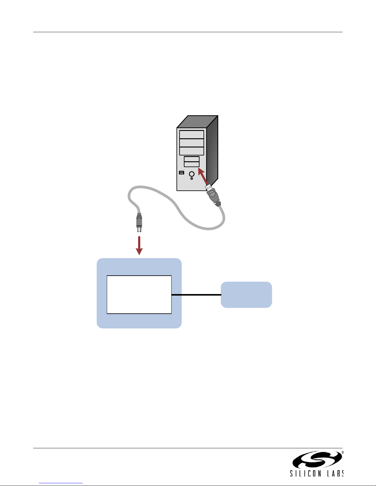
4. CP2110 Hardware Interface
Connect the CP2110 evaluation board to a PC as shown in Figure 1.
1. Connect one end of the USB cable to a USB Port on the PC.
2. Connect the other end of the USB cable to the USB connector on the CP2110 evaluation board.
3. Connect one end of the RS-232 serial cable to the DB-9 connector on the CP2110 evaluation board.
4. Connect the other end of the RS-232 serial cable to the tar get serial device.
2 Rev. 0.3
Figure 1. Hardware Setup
Page 3
CP2110-EK
5. CP2110 Software Interface
The CP2110 is an HID device that uses the standard HID functions available in the operating system. To facilitate
this process in Windows, Silicon Labs packaged the standard HID functions into the SLABHIDDevice DLL in the
CP2110 software package. The HID report structure for the CP2110 is customized for the device and is not
compatible with other HID report structures, like a m ouse or keyboard. AN434, “CP2110 Interface Specification”
describes the custom HID report structure for the CP2110, and AN433, “CP2110 HID to UART API Specification”
describes the API software functions that can be used to read or write data and control the CP2110 from the PC.
The software application described in “6. CP2110 Windows Application” provides an example of how to use these
functions.
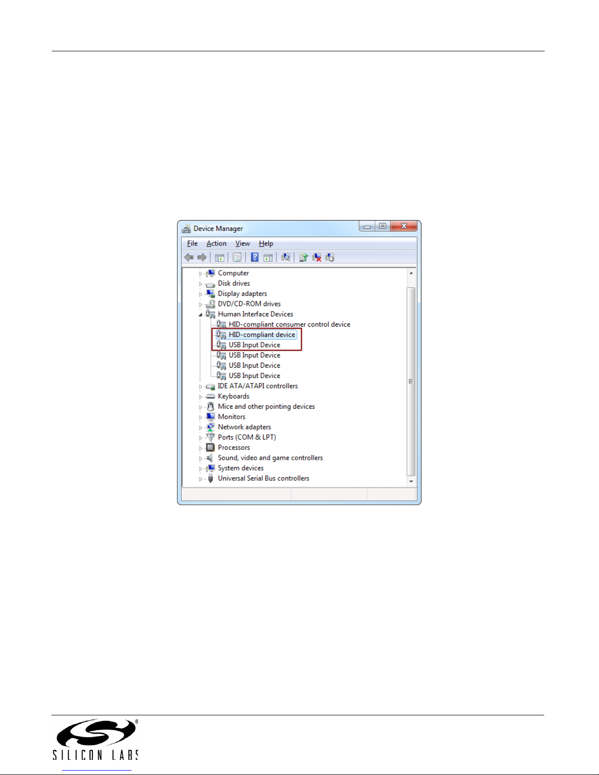
The CP2110 appears as an HID device in Device Manager as shown in Figure 2.
Figure 2. CP2110 in Device Manager
Rev. 0.3 3
Page 4

CP2110-EK
4
5
6
7
6. CP2110 Windows Application
The HIDUart application is an example application that uses the Windows CP2110 HID-to-UART DLL to transmit
and receive data with the CP2110. The application also has access to the CP2110’s GPIO pins. The HIDUart
application is installed as part of the SDK installation process (Section 3). The following steps describe how to start
the application and use some of the features.
1. Ensure that the hardware is connected to a Windows PC as shown in Section 4. If the device is properly connected,
the red SUSPEND LED on the CP2110 evaluation board will turn on.
2. Launch the HIDUart application, which is found by clicking StartAll ProgramsSilicon LaboratoriesHIDUart
Example.
3. In the application, configure the baud rate, data bits, parity, stop bits, and type of flow control using the drop-down
menus. This configuration should match the communication settings used by the serial device.
4. Click Connect to start communication between the application and the CP21 10 evaluation board. Once connected, the
USB descriptors retrieved from the device are shown under Device Information.
Figure 3. HIDUart Example Application after Connection
5. Type data in the T ransmit text box and click Transmit to send data from the PC to the serial device.
6. Send data from serial device to the PC. Any data sent by the serial device to the PC is automatically updated in the
Receive text box.
7. The HIDUart example automatically recognizes how the GPIO pins are configured and enables/disables the ability to
change and read the pin. The default configuration is shown in Figure 3. Use the Get and Set buttons to read and write
the GPIO pins’ latch values. For GPIO pins that are configured as outputs, setting the pin to logic low 0 will turn on the
corresponding LED on the CP2110 evaluation board.
4 Rev. 0.3
Page 5

CP2110-EK
U1
P2
P1
J9
J12
J5 J3
J6J7
J2
J4
D1
D0
D5
D4
D9
D8
D6
D7
D3
D2
D10
U2
J1
J8
www.silabs.com
SILICON LABS
CP2110-EB
7. Evaluation Board Overview
The
CP2110
preliminary software development. Numerous input/output (I/O) connections are provided to facilitate prototyping
using the evaluation board. Refer to
Evaluation Kit includes an evaluation board with a
Figure 4
for the locations of the various I/O connectors.
CP2110
device pre-installed for evaluation and
P1 DB9 connector for RS-232 interface
P2 USB connector for USB interface
J1 UART signal access connector
J2 VDD and VIO power connectors
J3 GPIO0 and GPIO1 LED connectors
J4 GPIO2 and GPIO3 LED connectors
J5 GPIO4 and GPIO5 LED connectors
J6 GPIO6 and GPIO7 LED connectors
J7 GPIO8 and GPIO9 LED connectors
J8 REGIN pin power connector
J9 SUSPEND
RED LED connector
J12 Self-Power mode VDD and GND access connectors
Figure 4. CP2110 Evaluation Board with Default Shorting Blocks Installed
7.1. LED Headers (J3, J4, J5, J6, J7)
Connectors J3, J4, J5, J6, and J7 are provided to allow access to the 10 GPIO pins on the CP2110. Place shorting
blocks on these headers to conn ect the GPIO pins to the 10 green LEDs D0 - D9. These LEDs can be used to
indicate active communications through the CP2110. Table 1 shows the LED corresponding to each header
position.
LED Pins LED Pins
GPIO0-D0 J3[3:4] GPIO4-D7 J5[1:2]
GPIO1-D1 J3[1:2] GPIO6-D4 J6[3:4]
GPIO2-D2 J4[3:4] GPIO7-D5 J6[1:2]
GPIO3-D3 J4[1:2] GPIO8-D8 J7[3:4]
GPIO4-D7 J5[3:4] GPIO9-D9 J7[1:2]
Table 1. J2 and J3 LED Locations
Rev. 0.3 5
Page 6

CP2110-EK
7.2. Universal Serial Bus (USB) Interface (P2)
A Universal Serial Bus (USB) connector (P2) is provided to facilitate connections to the USB interface on the
CP2110. See Table 2 for the USB pin definitions.
Table 2. USB Connector Pin Descriptions
Pin # Description
1 VBUS
2D–
3D+
4 GND (Ground)
7.3. UART Signals (P1, J1)
An RS-232 transceiver circuit and DB9 connector (P1) are provided on the e valuation board to connect the CP2110
virtual serial port to external serial devices. See Table 3 for the RS-232 P2 pin descriptions. The J1 connector is
provided to facilitate direct access to the CP2110’s UART signals. Shorting blocks on J1 are required to connect
the UART signals to P2. See Table 4 for J1 pin descriptions.
Table 3. RS-232 Pin Descriptions
Pin Signal
2 RXD Input Receive Data
3 TXD Output Transmit Data
5 GND Ground
7 RTS Output Request to Send
8 CTS Input Clear to Send
CP2110
Direction
Description
Table 4. J1 Pin Descriptions
Pins Signal
1-2 TXD Output Tr an sm it Da ta
3-4 RXD Input Receive Data
5-6 RTS Output Request to Send
7-8 CTS Input Clear to Send
CP2110
Direction
Description
6 Rev. 0.3
Page 7

CP2110-EK
7.4. VDD and VIO Power Connector (J2)
This header (J4) is included on the evaluation board to provide several power options. The following describes the
function of each pin:
Pins 1,3: Connects CP2110 VIO input (pin 5) to CP2110 VDD (pin 6). Remove the shorting block to power
VIO from an external source.
Pins 2,4: Connects the main +VDD_A net to the CP2110 VDD (pin 6). The main +VDD_A net powers the
RS-232 transceiver on the evaluation board.
7.5. REGIN Power Connector and Self-Powered Mode Connector (J8, J12)
The J8 header is used to connect the CP2110 REGIN pin (pin 7) to the VBUS source from the USB connector
(default) or to the CP2110 VDD pin (pin 6). When connected to the VBUS source, the device is intended for buspowered operation. When connected to the CP2110 VDD pin, the device is intended fo r self-powered operation.
When in self-powered operat i on , an e xt er na l p o wer s ou rc e can be connected to the J12 header to power the VDD
pin directly.
7.6. .SUSPEND LED Connector (J9)
The J9 header is used to connect the CP2110 SUSPEND pin (pin 17) to the D10 red LED. When the LED is on, the
device has enumerated with the PC operating normally. When the LED is off, the device has not yet enu merated or
is in the USB Suspend state.
Rev. 0.3 7
Page 8
CP2110-EK
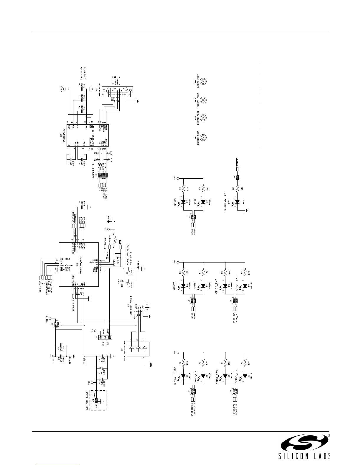
8. Schematic
8 Rev. 0.3
Figure 5. CP2110 Evaluation Board Schematic
Page 9

CP2110-EK
DOCUMENT CHANGE LIST
Revision 0.2 to Revision 0.3
Updated “1. Kit Contents” to change CD-ROM to
DVD.
Added “2. Relevant Documentation” and “5. CP2110
Software Interface”.
Updated “3. Software Setup” to point to the drivers
on the website.
Updated Fi gu re 1.
Updated Figure 3 with numbered steps matching the
instructions in “6. CP2110 Windows Application”.
9 Rev. 0.3
Page 10

CP2110-EK
The information in this document is believed to be accurate in all respects at the time of publication but is subject to change without notice.
Silicon Laboratories assumes no responsibility for errors and omissions, and disclaims responsibility for any consequences resulting from
the use of information included herein. Additionally, Silicon Laboratories assumes no responsibility for the functioning of undescribed features
or parameters. Silicon Laboratories reserves the right to make changes without further notice. Silicon Laboratories makes no warranty, representation or guarantee regarding the suitability of its products for any particular purpose, nor does Silicon Laboratories assume any liability
arising out of the application or use of any product or circuit, and specifically disclaims any and all liability, including without limitation consequential or incidental damages. Silicon Laboratories products are not designed, intended, or authorized for use in applications intended to
support or sustain life, or for any other application in which the failure of the Silicon Laboratories product could create a situation where personal injury or death may occur. Should Buyer purchase or use Silicon Laboratories products for any such unintended or unauthorized application, Buyer shall indemnify and hold Silicon Laboratories harmless against all claims and damages.
CONTACT INFORMATION
Silicon Laboratories Inc.
400 West Cesar Chavez
Austin, TX 78701
Tel: 1+(512) 416-8500
Fax: 1+(512) 416-9669
Toll Free: 1+(877) 444-3032
Please visit the Silicon Labs Technical Support web page:
https://www.silabs.com/support/pages/contacttechnicalsupport.aspx
and register to submit a technical support request.
Patent Notice
Silicon Labs invests in research and development to help our customers differentiate in the market with innovative low-power, small size, analogintensive mixed-signal solutions. Silicon Labs' extensive patent portfolio is a testament to our unique approach and world-class engineering team.
Silicon Laboratories and Silicon Labs are trademarks of Silicon Laboratories Inc.
Other products or brandnames mentioned herein are trademarks or registered trademarks of their respective holders.
10 Rev. 0.3
 Loading...