

Page 1

C8051T63x-DK
C8051T63X DEVELOPMENT KIT USER’S GUIDE
1. Kit Contents
The C8051T63x Development Kit contains the following items:
C8051T630 Motherboard
C8051T630 QFN 20-pin Socket Daughter Board for programming C8051T63x devices
C8051T630 Emulation Daughter Board with C8051F336 installed
Five C8051T630-GM samples
C8051T63x Development Kit Quick-Start Guide
Product information CD-ROM including the following:
Silicon Laboratories Integrated Development Environment (IDE)
Evaluation version of Keil 8051 development tools (macro assembler, linker, C compiler)
Source code examples and register definition files
Documentation
AC-to-DC universal power adapter
Two USB cables
2. About the Daughter Boards
The C8051T63x Development Kit includes an Emulation Daughter Board (EDB) and a QFN Socket Daughter
Board (QFN-DB). The EDB has an installed C8051F336 device, which is a Flash-based device that can be used
for the majority of C8051T63x code development. The QFN-DB is intended to allow both programming and
system-level debugging of C8051T63x devices directly.
A C8051T63x device cannot be erased once it has been program med; so, it is advisab le to use the C80 51F 336 for
the majority of code development. Refer to “AN339: Differences between the C8051F336 and the C8051T63x
device family” for more details on how the C8051F336 can be used to develop code for the C8051T63x device
family.
Rev. 0.1 1/08 Copyright © 2008 by Silicon Laboratories C8051T63x-DK
Page 2
C8051T63x-DK
PWR
P3
DEBUG
J2
SW
J12
R8
SILICON LABS
www.silabs.com
RESET
P4
COMM
P5
P1
P2
J3
LED
J11
J7
J10
J8
VDD_PWR
J6
VDD_PWR
VDD_PWR
VDD_PWR
+3VD
VDD_EXT
VDD_F326
VDD_CCP2103
USB ACTIVE
TX_F326
P0.4
P0.5
RX_CP2103 TX_CP2103
RX_F326
CTS_F326
P1.1
P1.2
RTS_CP2103
CTS_CP2103
RTS_F326
VPP
P1.3
P0.7
PWR
D10
DEBUG
PWR
RUN / STOP
D7
D12
D11
J4
SW
J9
J5
AC Adapter
USB Cable
Place shorting blocks on
J7 and J6 as shown.
F336
C8051T630 EDB
C8051T630-MB
J13
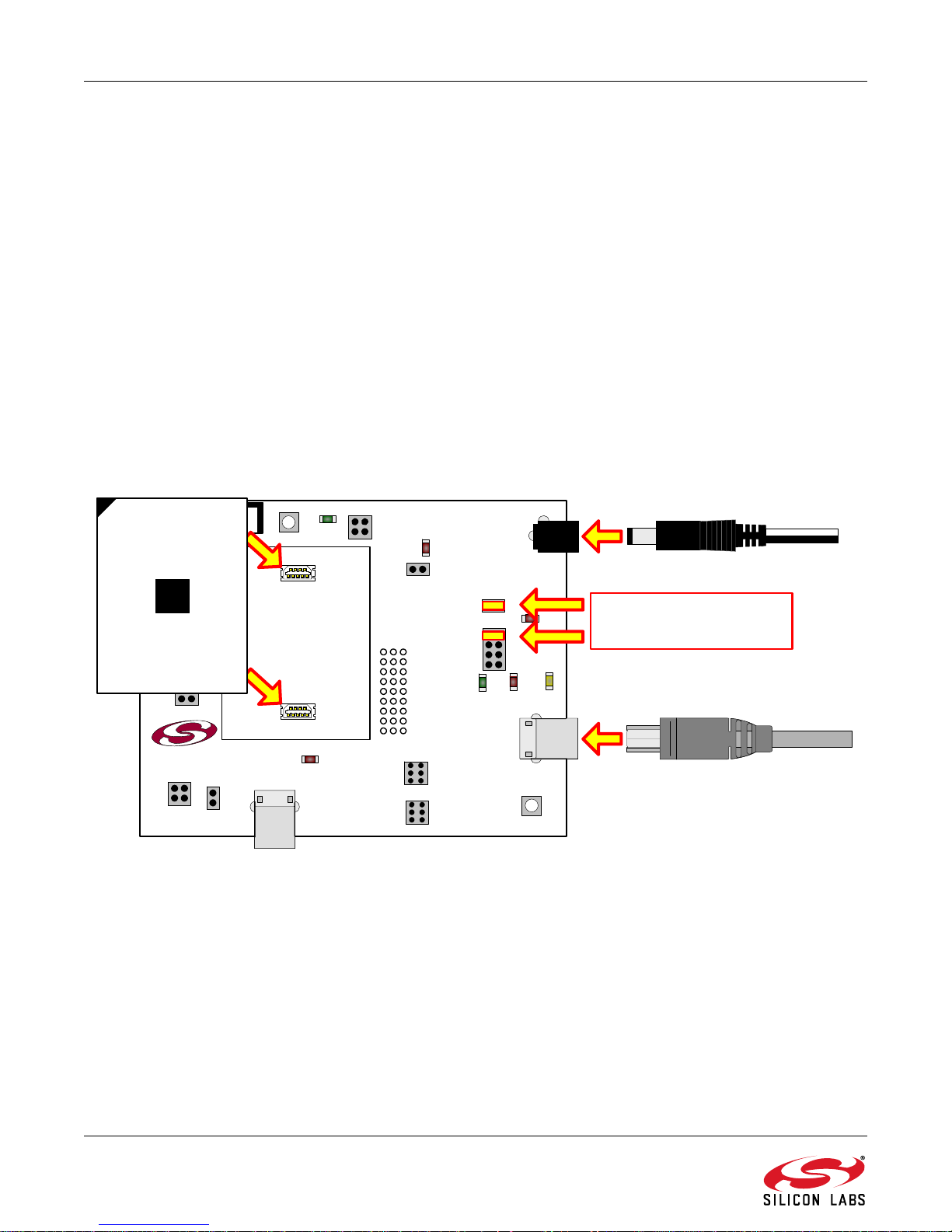
3. Hardware Setup
See Figure 1 for a diagram of the hardware configuration.
1. Attach the desired daughter board to the motherboard at connectors P1 and P2.
2. If using the QFN Socket Daughter Board, place the device to be programmed into the socket.
3. Place shorting blocks on J7 and the +3VD-VDD_PWR jump er pair on J6, as shown in Figu re 1.
4. Connect the motherboard’s P5 USB connector to a PC running the Silicon Laboratories IDE using the USB
Cable.
5. Connect the ac-to-dc power adapter to connector P3 on the motherboard .
Notes:
• Use the Reset icon in the IDE to reset the target when connected during a debug session.
• Remove power from the motherboard and remove the USB cable before removing a daughter board from the
motherboard. Connecting or disconnecting a daughter board when the power adapter or USB cable are connected can
damage the motherboard, the daughter board, or the socketed devic e.
• Remove power from the motherboard and remove the USB cable before removing a C8051T63x device from the socket.
Inserting or removing a device from the socket when the power adapter or USB cable are connected can damage the
motherboard, the daughter board, or the socketed device.
• The above hardware setup instructions configure the development system to be powered through the onboard 3.3 V
regulator . For other power options, see Section 7.3.
Figure 1. Hardware Setup (Emulation Daughter Board)
2 Rev. 0.1
Page 3

C8051T63x-DK
4. Software Overview
The included CD-ROM contains the Silicon Laboratories Integrated Development Environment (IDE), Keil software
8051 tools, Virtual COM Port drivers for the CP21 0x USB to UAR T Bridge, and additiona l document ation. Insert the
CD-ROM into your PC's CD-ROM drive. An installer will automatically launch, allowing you to install the IDE
software or read documentation by clicking buttons on t he installation panel. If the installer does not automatically
start when you insert the CD-ROM, run autorun.exe found in the root directory of the CD-ROM. Refer to the
ReleaseNotes.txt file on the CD-ROM for the latest information regarding the CD contents.
4.1. Development Tools Installation
To install the IDE, utilities, and code examples, perform the following steps:
1. Click on the "Install Development Tools" button on the installation utility's startup screen.
2. In the Kit Selection box that appears, choose the C8051T630-DK development kit from the list of options.
3. In the next screen, choose “Components to be Installed”.
Note: Selecting the action that reads "Install CP210x Drivers" will launch a program described in “4.2. CP210x USB to UART
VCP Driver Installation”.
4. Installers selected in Step 3 will execute in sequence, prompting the user as they install programs,
documentation, and drivers.
4.2. CP210x USB to UART VCP Driver Installation
The C8051T630 Motherboard includes a Silicon Laboratories CP2103 USB-to-UART Bridge Controller. Device
drivers for the CP2103 need to be installed before PC software such as HyperTerminal can communicate with the
board over the USB connection. If the "Install CP210x Drivers" option was selected during installation, this will
launch a driver “unpacker” utility.
1. Follow the steps to copy the driver files to the desired location . The default directory is C:\SiLabs\MCU\CP210x.
2. The final window will give an option to install the driver on the target system. Select the “Launch the CP210x VCP Driver
Installer” option if you are ready to install the driver.
3. If selected, the driver installer will now launch, providing an option to specify the driver installation location. After pressing
the “Install” button, the installer will search your system for copies of previously installed CP210x Virtual COM Port drivers. It
will let you know when your system is up to date. The driver files included in this installation have been certified by Microsoft.
4. If the “Launch the CP210x VCP Driver Installer” option was not selected in step 3, the installer can be found in the location
specified in step 2, by default C:\SiLabs\MCU\CP210x\Windows_2K_XP_S2K3_Vista. At this location run
CP210xVCPInstaller.exe.
5. To complete the installation process, connect the included USB cable between the host computer and the COMM USB
connector (P4) on the C8051T630 Motherboard. Windows will automatically finish the driver installation. Information
windows will pop up from the taskbar to show the installation progress.
6. If needed, the driver files can be uninstalled by selecting “Silicon Laboratories CP210x USB to UART Bridge (Driver
Removal) option in the “Add or Remove Programs” window.
4.3. Silicon Laboratories IDE
The Silicon Laboratories IDE integrates a source-code editor, source-level debugger, and an in-system Flash
programmer. The Keil demonstration toolset includes a compiler, linker, and assembler and easily integrates into
the IDE. The use of other third-party compilers and assemblers is also supported.
4.3.1. IDE System Requirements
Silicon Laboratories IDE requirements include the following:
Pentium-class host PC running Microsoft Windows 2000 or later
One available USB port
Rev. 0.1 3
Page 4
C8051T63x-DK
4.3.2. Third-Party Toolsets
The Silicon Laboratories IDE has native support for many 8051 compilers. Natively-supported tools are as follows:
Keil
IAR
Raisonance
Tasking
Hi-Tech
SDCC
The demonstration applications for the C8051T63x development kit are written for the Keil and SDCC to olsets.
4.4. Keil Demonstration Toolset
4.4.1. Keil Assembler and Linker
The Keil demonstration toolset assembler and linker place no restrictions on code size.
4.4.2. Keil Demonstration C51 C Compiler
The evaluation version of the C51 compiler is the same as the full version with the following limitations: (1)
Maximum 4 kB code generation, (2) There is no floating point library included. When installed from the CD-ROM,
the C51 compiler is initially limited to a code size of 2 kB, and programs start at code address 0x0800. Refer to
“AN104: Integrating Keil Tools into the Silicon Labs IDE" for instructions to change the limitation to 4 kB and have
the programs start at code address 0x0000.
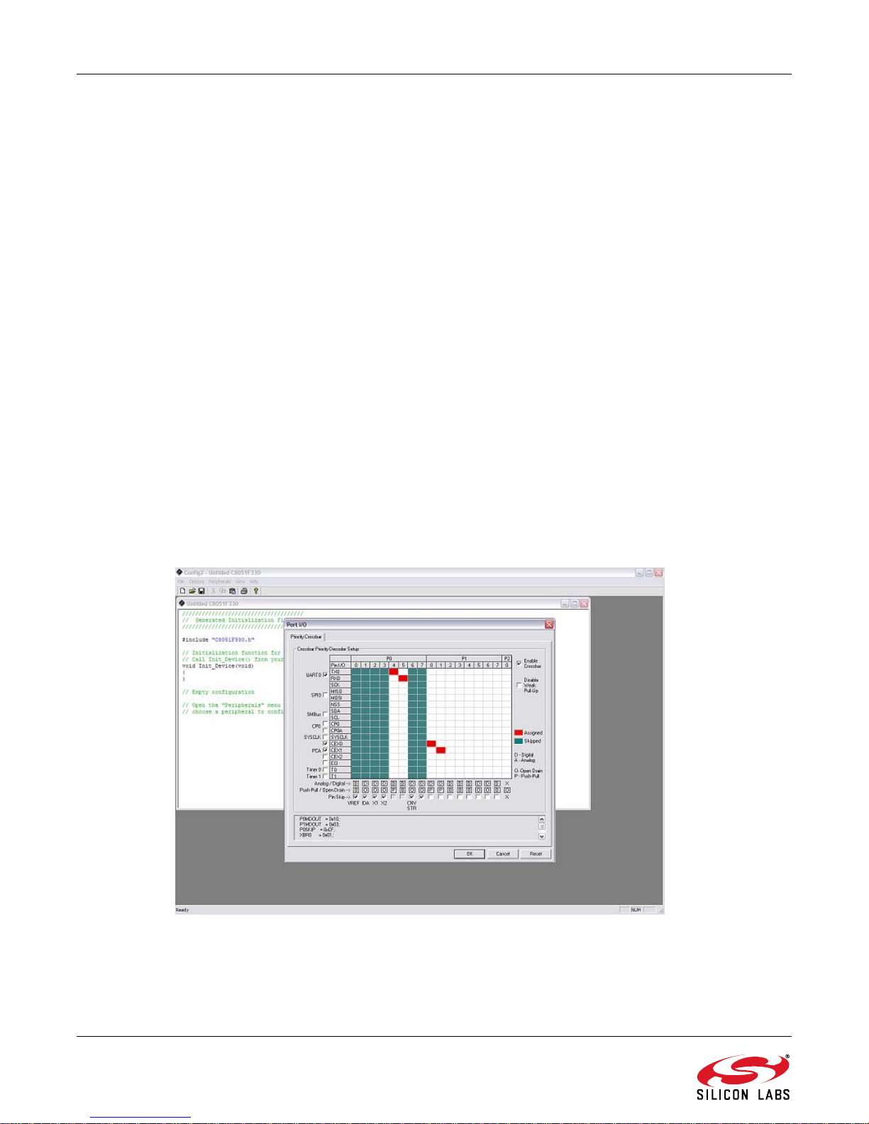
4.5. Configuration Wizard
Configuration Wizard is a code generation tool for all Silicon Laboratories devices. Code is generated through the
use of dialog boxes for each device peripheral as shown in Figure 2.
Figure 2. Configuration Wizard 2 Utility
4 Rev. 0.1
Page 5

C8051T63x-DK
The Configuration Wizard utility helps accelerate development by automatically generating initialization source
code to configure and enable the on-chip reso urces ne eded by most design project s. In just a few steps, th e wizard
creates complete startup code for a specific Silicon Laboratories MCU. The program is configurable to provide the
output in C or assembly language.
For more information, refer to the Configuration Wizard documentation. Documentation and software is available
on the kit CD and from the downloads webpage: www.silabs.com/mcudownloads.
4.6. Keil uVision2 and uVision3 Silicon Laboratories Drivers
As an alternative to the Silicon Laboratories IDE, the µVision debug driver allows the Keil µVision2 and µVision3
IDEs to communicate with Silicon Laboratories’ on-chip debug logic. In-system Flash memory programming
integrated into the driver allows for rapid updating of target code. The µVision2 and µVision3 IDEs can be used to
start and stop program execution, set breakpoints, check variables, inspect and modify memory contents, and
single-step through programs runn ing on the ac tu al target ha rd wa re .
For more information, refer to the µVision driver documentation. The documentation and software are available on
the kit CD and from the downloads webpage: www.silabs.com/mcudownloads.
4.7. ToolStick Terminal
The onboard debug circuitry provides both an in-system programming and debugging interface and a
communications interface to the target microcontroller's UART. The ToolStick Terminal s oftware can access the
debug hardware's communications path and provides a terminal-like interface on the PC. Note that for concurrent
debugging and UART communications, the CP2103 USB-to-UART bridge is also included onboard.
In addition to the standard terminal functions (Send File, Receive File, Change Baud Rate), two GPIO pins on the
target microcontroller can be controlled using the terminal for either RTS/CTS handshaking or softwareconfigurable purposes. The ToolStick Terminal software is available on the downloads webpage: www.silabs.com/
mcudownloads.
Rev. 0.1 5
Page 6

C8051T63x-DK
5. Using the Keil Software 8051 Tools with the Silicon Laboratories IDE
To perform source-level debugging with the IDE, configure the Keil 8051 tools to generate an absolute object file in
the OMF-51 format with object extensions and debug records enabled. Build the OMF-51 absolute object file by
calling the Keil 8051 tools at the command line (e.g., batch file or make file) or by using the project manager built
into the IDE. The default configuration when using the Silicon Laboratories IDE project manager enables object
extension and debug record generation. Refer to "AN104: Integrating Keil 8051 Tools into the Silicon Labs IDE" in
the SiLabs\MCU\Documentation\Appnotes directory on the CDROM for additional information on using the Keil
8051 tools with the Silicon Laboratories IDE.
To build an absolute object file using the Silicon Laboratories IDE project manager, you must first create a project.
A project consists of a set of files, IDE configuration, debug views, and a target build configuration (list of files and
tool configurations used as input to the assembler, compiler, and linker when building an output object file). The
following sections illustrate the steps necessary to manually create a project with one or more source files, build a
program, and download it to the target in preparation for debugging. (The IDE will automatically create a single-file
project using the currently open and active source file if you select Build/Make Project before a project is defined.)
5.1. Creating a New Project
1. Select “ProjectNew Project” to open a new project and reset all configuration settings to default.
2. Select “FileNew File” to open an editor window. Cr eate your source file(s) and save the file(s) with a
recognized extension, such as .c, .h, or .asm, to enable color syntax highlighting.
3. Right-click on "New Project" in the Project Window. Select “Add Files to Project”. Select files in the file browser,
and click “Open”. Continue adding files until all project files have been added.
4. For each of the files in the Project Window that you want assembled, compiled, and linked into the target build,
right-click on the file name, and select “Add File to Build”. Each file will be assembled or compiled as
appropriate (based on file extension) and linked into the build of the absolute object file.
Note: If a project contains a large number of files, the "Group" feature of the IDE can be used to organize them. Righ t-click on
"New Project" in the Project Window. Select “Add Groups to Project”. Add predefined groups or add customized groups.
Right-click on the group name, and choose “Add File to Group”. Select files to be ad ded. Continue adding files until all
project files have been added.
5.1.1. Building and Downloading the Program for Debugging
1. Once all source files have been added to the target build, build the project by clicking on the “Build/Make
Project” button in the toolbar or by selecting “ProjectBuild/Make Project” from the menu.
Note: After the project has been built the first time, the Build/Make Project command will only build the files that have been
changed since the previous build. To rebuild all files and project dependencies, click on the “R ebuild All” button in the
toolbar or select “Project
2. Before connecting to the target device, several connection options may need to be set. Open the Connection
Options window by selecting “OptionsConnection Options...” in the IDE menu. First, select the "USB Debug
Adapter" option. The USB Debug circuitry is integrated onto the C8051T630 Motherboard.
3. Next, the correct debug interface must be selected. C8051T63x family devices and the F336 all use the Silicon
Labs "C2" 2-wire debug interface. Once all the selections are made, click the OK button to close the window.
4. Click the “Connect” button in the toolbar, or select “DebugConnect” from the menu to connect to the de vice.
5. Download the project to the target by clicking the “Download Code” button in the toolbar.
Note: To enab le automatic downloading if the program build is successful, select “Enable Automatic Connect/Download after
Build” in the “ProjectT arget Build Configuration” dialog. If errors occur during the build process, the IDE will not attempt
the download.
6. Save the project when finished with the debug session to preserve the current target build configuration, editor
settings, and the location of all open debug views. To save the project, select “ProjectSave Project As...” from
the menu. Create a new name for the project, and click on “Save”.
Rebuild All” from the menu.
6 Rev. 0.1
Page 7

C8051T63x-DK
6. Example Source Code
Example source code and register definition files are pro vided by default in the SiLabs\MCU\Examples\C8051T63x
directory during IDE installation. These files may be used as a template for code development.
6.1. Register Definition Files
Register definition files C8051T630.inc, C8051T630_defs.h, and compiler_defs.h, define all SFR registers and bit
addressable control/status bits. They are installed by default into the SiLabs\MCU\Examples\C8051T63x directory
during IDE installation. The register and bit names are identical to those used in the C8051T63x data sheet. The
register definition files are also installe d in the de fa ult s ear ch path used by the Keil Software 8051 tools. Therefor e,
when using the Keil 8051 tools included with the development kit (A51, C51), it is not necessary to copy a register
definition file to each project's file directory.
6.2. Blinking LED Example
The example source files T63x_Blinky.asm and T63x_Blinky.c show examples of several basic C8051T63x
functions. These include disabling the watchdog timer (WDT), configuring the Por t I/O crossb ar, configuring a timer
for an interrupt routine, initializing the system clock, and configuring a GPIO port. When compiled/assembled and
linked, these programs flash the green LED on the C8051T630 Motherboard about ten times a second using the
interrupt handler with a timer.
7. Development Boards
The C8051T63x Development Kit includes a motherboard that interfaces to various daughter boards. The
C8051T630 Emulation Daughter Board contains a C8051F336 device to be used for preliminary software
development. The C8051T630 Socket Daughter Board allows programming and evaluation of the actual
C8051T63x family of devices. Numerous input/output (I/O) connections are provided on the motherboard to
facilitate prototyping. Figure 3 shows the C8051T630 Motherboard and indicates locations for various I/O
connectors. Figure 4 shows the factory default shorting block positions. Figures 5 and 6 show the available
C8051T630 daughter boards.
P1, P2 Daughter board connection
P3 Power connector that accepts input from 7.5 V dc to 15 V dc unregulated power adapter
P4 USB connector for UART to USB communications interface
P5 USB Debug interface connector
J1 Analog I/O terminal block
J2 Port 0 header
J3 Port 1 header
J4 Port 2 header
J5 Connects P0.1 (IDAC) pin to grounded resistor to produce voltage output at IDAC pin.
J6 Power supply selection header (See “7.3. Power Supply Headers (J6 and J7)”)
J7 Power supply enable header that connects power source selected on J6 to the board's main
power supply net
J8 Communications interface control signal header
J9 Connects port pin P0.7 to the switch labeled "SW" and port pin P1.3 to the LED labeled "LED"
J10 Communications interface data signal header
J11 VPP supply connection used when programming EPROM devices
J12 Connects potentiometer to the port pin, P1.6
J13 Additional connections to ground
Rev. 0.1 7
Page 8

C8051T63x-DK
PWR
P3
DEBUG
J2
SW
J12
R8
SILICON LABS
www.silabs.com
RESET
P4
COMM
P5
P1
P2
J3
LED
J11
J7
J10
J8
VDD_PWR
J6
VDD_PWR
VDD_PWR
VDD_PWR
+3VD
VDD_EXT
VDD_F326
VDD_CCP2103
USB ACTIVE
TX_F326
P0.4
P0.5
RX_CP2103 TX_CP2103
RX_F326
CTS_F326
P1.1
P1.2
RTS_CP2103
CTS_CP2103
RTS_F326
VPP
P1.3
P0.7
PWR
D10
DEBUG
PWR
RUN / STOP
D7
D12
D11
SW
J9
J5
C8051T630-MB
Pin 1
Pin 1
Pin 1
Pin 1
Pin 1
Pin 1
Pin 1
Pin 1
Pin 1
Pin 1
Pin 1
J4
J13
Pin 1
J1
Figure 3. C8051T630 Motherboard
8 Rev. 0.1
Page 9

C8051T63x-DK
PWR
P3
DEBUG
J2
SW
J12
R8
SILICON LABS
www.silabs.com
RESET
P4
COMM
P5
P1
P2
J3
LED
J11
J7
J10
J8
VDD_PWR
J6
VDD_PWR
VDD_PWR
VDD_PWR
+3VD
VDD_EXT
VDD_F326
VDD_CCP2103
USB ACTIVE
TX_F326
P0.4
P0.5
RX_CP2103 TX_CP2103
RX_F326
CTS_F326
P1.1
P1.2
RTS_CP2103
CTS_CP2103
RTS_F326
VPP
P1.3
P0.7
PWR
D10
DEBUG
PWR
RUN / STOP
D7
D12
D11
SW
J9
J5
C8051T630-MB
J4
J13
J1
Figure 4. C8051T630 Motherboard Default Shorting Block Positions
Rev. 0.1 9
Page 10

C8051T63x-DK
F336
C8051T630 EDB
U1
SILICON LABS
www.silabs.com
C8051T630 QFN20 SKT DB
SILICON LABS
www.silabs.com
U1
Pin 1
Figure 5. C8051T630 Emulation Daughter Board
Figure 6. C8051T630 QFN20 Socket Daughter Board
10 Rev. 0.1
Page 11

C8051T63x-DK
7.1. System Clock Sources
The C8051T63x devices feature a calibrated internal oscillator that is enabled as the system clock source on reset.
After reset, the internal oscillator operates at a frequency of 24.5 MHz (±2%) by default, but may be configured by
software to operate at other frequencies. Therefore, in many applications, an external oscillator is not required.
However, if you wish to operate the C8051T63x device at a frequency not available with the internal oscillator, an
external oscillator source may be used. Refer to the C8051T63x data sheet for more information on configuring the
system clock source.
7.2. Switches, LEDs, Potentiometer, and IDAC Resistor
Two switches are provided on the motherboard. The RESET switch is connected to the RST pin of the C8051T63x.
Pressing RESET puts the device into its hardware-reset state. The switch labeled “SW” can be connected to the
C8051T63x's general purpose I/O (GPIO) pin P0.7 through header J9. Pressing this switch generates a logic low
signal on the port pin. Remove the shorting block from the J9 header to disconnect the switch from the port pin.
Six LEDs are also provided on the motherboard. The red LED labeled “PWR” (D4), is used to indicate a power
connection to the motherboard. The green LED labeled “RUN” (D10) turns on when the debug circuitry is in a
running state; the red LED labeled “STOP” (D11) turns on when the debug circuitry is in a halted state, and the
orange LED labeled “DEBUG PWR” (D12) indicates whether the debug adapter circuit is being powered through
P5's USB connector. The red LED labeled “VPP” (D7) indicates when the VPP programming voltage is being
applied to the device. The green LED, labeled "LED" (D1), can be connected to the C8051T63x's GPIO pin through
header J9. Remove the shorting block from the header to disconnect the LED from the port pin. The red LED
labeled "USB ACTIVE" (D2) will turn on whenever the CP2103 USB-to-UART bridge is connected to a PC and has
successfully completed enumeration.
Also included on the C8051T63x motherboard is a 10 k thumbwheel rotary potentiometer, reference number R8.
The potentiometer can be connected to the C8051T63x's P1.6 pin through the J12 header. Remove the shorting
block from the header to disconnect the potentiometer from the port pin.
A 1 kresistor, reference number R20, is included on the C8051T63x Motherboard to provide a current path to
ground for the IDAC. The resistor can be connected to the IDAC output pin (P0.1) through the J5 header.
Table 1 lists the port pins and headers corresponding to the switches, LEDs, potentiometer, and IDAC resistor.
Table 1. Motherboard I/O Descriptions
Description Component Name I/O Header
SW SW1 Daughter Card's P0.7 J9 [3-4]
RESET SW2 Daughter Card's RST/C2CK None
Green LED labeled "LED" D1 Daughter Card's P1.3 J9 [1-2]
Green LED labeled "USB ACTIVE" D2 U2 CP2103's SUSPEND None
Red LED labeled "PWR" D4 Daughter Card's VDD J6, J7
Red LED labeled “VPP” D7 Daughter Card's P0.2 J11
Green LED labeled "RUN" D10 Debug Adapter Signal None
Red LED labeled "STOP" D11 Debug Adapter Signal None
Orange LED labeled "DEBUG PWR" D12 Debug Adapter Signal None
Potentiometer R8 Daughter Card's P1.6 J12
IDAC Resistor R20 Daughter Card's P0.1 J5
Rev. 0.1 11
Page 12

C8051T63x-DK
J7
VDD_PWR
J6
VDD_PWR
VDD_PWR
VDD_PWR
+3VD
VDD_EXT
VDD_F326
VDD_CP2103
J7
VDD_PWR
J6
VDD_PWR
VDD_PWR
VDD_PWR
+3VD
VDD_EXT
VDD_F326
VDD_CP2103
J7
VDD_PWR
J6
VDD_PWR
VDD_PWR
VDD_PWR
+3VD
VDD_EXT
VDD_F326
VDD_CP2103
J7
VDD_PWR
J6
VDD_PWR
VDD_PWR
VDD_PWR
+3VD
VDD_EXT
VDD_F326
VDD_CP2103
+3.3V Regulator Power
(From P3)
CP2103 Regulator Power
(From USB at P4)
Debug Circuit Power
(From US B at P 5)
External Power Source
(From J1 Connector)
7.3. Power Supply Headers (J6 and J7)
The main power supply of the motherboard, which is used to power the daughter board, can be provided by either
the USB Debug Adapter’s on-chip voltage regulator, the CP2103 USB-to-UART bridge’s on-chip voltage regulator,
P3 and its associated circuitry, or an external voltage applied to the VDD_EXT connection on J1. To select a power
supply, place a shorting block on J6 across the appropriate pin pair, as shown in Figure 7. To connect the main
power supply to an attached daughter board, place a shorting block across J7.
Notes:
1. Only one shorting block should be placed on J6 at a time.
2. To use the CP2103’s voltage regulator as the board's power supply, a USB cable must be connected to P4,
and the USB ACTIVE LED (D2) must be on.
3. To use the USB Debug Adapter ’s voltage regulator as the board's power supply, a USB cable must be
connected to P5, and the DEBUG PWR LED (D12) must be on.
Figure 7. J6 and J7 Shorting Block Configuration for Power Options
7.4. USB Debug Adapter (DEBUG/P5)
A Universal Serial Bus (USB) connector (P5) provides the onboard debug and programming interface. The debug/
programming MCU and ass ociated circuitry are powered th rough the USB connector, which can also supply the
rest of the motherboard by routing the USB Debug Adapter's power through J6. The USB Debug Adapter also
provides a data communications interface that can be used when the debug adapter is not debugging or
programming a C8051T63x device.
7.5. UART to USB Communications Interfaces
The C8051T630 Motherboard provides UART to USB communications interfaces through both the CP2103 USBto-UART bridge device and the communications interface of the USB Debug Adapter.
The CP2103 bridge device connects to a PC through the USB connector labeled “COMM” (P4). This USB
connector supplies power to the CP2103 and can supply power to the rest of the motherboard by configuring J6
and J7 as shown in Figure 7. To use the CP2103 as a communications interface, the CP2103 Virtual COM Port
drivers must be installed on a PC.
The USB Debug Adapter's communications interface connects to a PC through P5. Access to the USB Debug
Adapter's communications interface is provided by the Windows program called “ToolStick Terminal”, which is
available for download for free from the Silicon Laboratories website. See the ToolStick Terminal help file for
information on how to use ToolStick Terminal.
7.6. Communications Interface Selector Headers (J10 and J8)
The C8051T630 Motherboard routes the C8051T63x's P0.4 (UART TX) and P0.5 (UART RX) to J10, where those
signals can be connected to either the CP2103 USB-To-UART bridge or the USB Debug Adapter. The
motherboard also allows the C8051T63x's P1.1 and P1.2 to be used as the UART control signals, CTS and RTS.
These two signals are routed to J8, where they can b e conne cted to eithe r the CP21 03 or the USB De bug Adapter.
The jumper options for using either the CP2103 or the Debug Adapter circuit for UART communications can be
found in Figure 8.
12 Rev. 0.1
Page 13

C8051T63x-DK
CTS_F326
P1.1 P1.2
RTS_CP2103 CTS_CP2103
RTS_F326
J8
TX_F326
P0.4 P0.5
RX_CP2103 TX_CP2103
RX_F326
J10
CP2103 Bridge
(USB Connection at P4)
CTS_F326
P1.1 P1.2
RTS_CP2103 CTS_CP2103
RTS_F326
J8
TX_F326
P0.4 P0.5
RX_CP2103 TX_CP2103
RX_F326
J10
Debug Adapter Comms
(USB Connection at P5)
Figure 8. Shorting Block Configuration for UART Communication Options
7.7. PORT I/O Connectors (J2, J3 and J4)
Each of the C8051T63x's I/O pins, as well as +3VD and GND, are routed to headers J2 through J4. J2 connects to
the microcontroller's Port 0 pins, J3 connects to Port 1, and J4 connects to Port 2.
7.8. Analog I/O (J1)
Three of the C8051T63x target device's port pins are connected to the J1 terminal block. The terminal block also
allows users to input an external voltage that can be used as the power supply of the boar d. Refer to Table 2 for the
J1 terminal block connections.
7.9. VPP Connection (J11)
The C8051T63x devices require a special 6.5 V programming voltage applied to the VPP pin during device
programming. The VPP pin on these devices is shared with P0.2. During programming, the VPP voltage is
automatically enabled when needed. Header J11 is provided to allow the user to disconnect the programming
circuitry from the VPP/P0.2 pin to avoid interfering with the normal application operation of P0.2. When
programming the device, J11 should be shorted with a shorting block . When running normal ap plication co de, J11
can be removed.
7.10. Using Alternate Supplies with the C8051T63x Development Kit
For most evaluation purposes, the onboard 3.3 V supply regulator is sufficient to be used as a VDD power supply.
However, in application s where a dif ferent su pply volt age is desired ( e.g., 1.8 V), an external supply voltag e can be
applied to the board at the analog connector (J1).
Notes:
1. When programming a C8051T63x device, the onboard 3.3 V regulator should be used for VDD.
2. If an external supply voltage is desired, the shorting block on J6 should be placed so that th e pi n 3 (VDD_EXT)
is shorted to pin 4 (VDD_PWR).
Table 2. J1 Terminal Block Descriptions
Pin # Description
1 GND (Ground)
2 P0.1/IDAC
3 P1.6 (Analog Input)
4 P0.0/VREF
5 VDD_EXT (routed to header J6)
Rev. 0.1 13
Page 14

C8051T63x-DK
8. Schematics
14 Rev. 0.1
Figure 9. C8051T630 Motherboard Schematic (1 of 2)
Page 15

C8051T63x-DK
Figure 10. C8051T630 Motherboard Schematic (2 of 2)
Rev. 0.1 15
Page 16

C8051T63x-DK
16 Rev. 0.1
Figure 11. C8051T630 Emulation Daughter Board Schematic
Page 17

C8051T63x-DK
Figure 12. C8051T630 QFN-20 Daughter Board Schematic
Rev. 0.1 17
Page 18

Simplicity Studio
One-click access to MCU and
wireless tools, documentation,
software, source code libraries &
more. Available for Windows,
Mac and Linux!
IoT Portfolio
www.silabs.com/IoT
Disclaimer
Silicon Laboratories intends to provide customers with the latest, accurate, and in-depth documentation of all peripherals and modules available for system and software implementers
using or intending to use the Silicon Laboratories products. Characterization data, available modules and peripherals, memory sizes and memory addresses refer to each specific
device, and "Typical" parameters provided can and do vary in different applications. Application examples described herein are for illustrative purposes only. Silicon Laboratories
reserves the right to make changes without further notice and limitation to product information, specifications, and descriptions herein, and does not give warranties as to the accuracy
or completeness of the included information. Silicon Laboratories shall have no liability for the consequences of use of the information supplied herein. This document does not imply
or express copyright licenses granted hereunder to design or fabricate any integrated circuits. The products must not be used within any Life Support System without the specific
written consent of Silicon Laboratories. A "Life Support System" is any product or system intended to support or sustain life and/or health, which, if it fails, can be reasonably expected
to result in significant personal injury or death. Silicon Laboratories products are generally not intended for military applications. Silicon Laboratories products shall under no
circumstances be used in weapons of mass destruction including (but not limited to) nuclear, biological or chemical weapons, or missiles capable of delivering such weapons.
Trademark Information
Silicon Laboratories Inc., Silicon Laboratories, Silicon Labs, SiLabs and the Silicon Labs logo, CMEMS®, EFM, EFM32, EFR, Energy Micro, Energy Micro logo and combinations
thereof, "the world’s most energy friendly microcontrollers", Ember®, EZLink®, EZMac®, EZRadio®, EZRadioPRO®, DSPLL®, ISOmodem ®, Precision32®, ProSLIC®, SiPHY®,
USBXpress® and others are trademarks or registered trademarks of Silicon Laboratories Inc. ARM, CORTEX, Cortex-M3 and THUMB are trademarks or registered trademarks of
ARM Holdings. Keil is a registered trademark of ARM Limited. All other products or brand names mentioned herein are trademarks of their respective holders.
Silicon Laboratories Inc.
400 West Cesar Chavez
Austin, TX 78701
USA
SW/HW
www.silabs.com/simplicity
Quality
www.silabs.com/quality
Support and Community
community.silabs.com
http://www.silabs.com
 Loading...