

Page 1

C8051T620/2-DK
C8051T620/2 DEVELOPMENT KIT USER’S GUIDE
1. Kit Contents
The C8051T620 and C8051T622 Development Kits contain the following items:
C8051T62x Motherboard
C8051T62x Emulation Daughter Board with C8051F34A installed
Socket Daughter Board (one of the following):
C8051T62x QFN 32-pin (C8051T620DK)
C8051T622 QFN 24-pin (C8051T622DK)
Twenty device samples (one of the following):
C8051T620-GM (C8051T620DK)
C8051T622-GM (C8051T622DK)
C8051Txxx Development Kit Quick-Start Guide
Product information CD-ROM includes:
Silicon Laboratories Integrated Development Environment (IDE)
Evaluation version of 8051 development tools (macro assembler, linker, C compiler)
Source code examples and register definition files
Documentation
AC-to-DC universal power adapter
Two USB cables
2. About the Daughter Boards
The C8051T620 and C8051T622 Development Kits include an Emulation Daughter Board (EDB) and a QFN
Socket Daughter Board (QFN-DB). The EDB has an installed C8051F34A device, which is a Flash-based device
that can be used for the majority of C8051T62x/32x code development. The QFN-DB is intended to allow both
programming and system-level debugging of C8051T62x/32x devices directly.
A C8051T62x/32x device cannot be erased once it has been programmed; so, it is advisable to use the
C8051F34A for the majority of code development. Refer to “AN368: Differences between the C8051F34A and the
C8051T62x and C8051T32x Device Families” for more details on how the C8051F34A can be used to develop
code for the C8051T62x/32x device families.
Rev. 0.4 12/10 Copyright © 2010 by Silicon Laboratories C8051T620/2-DK
Page 2
C8051T620/2-DK
P3
SILICON LABS
www.silabs.com
RESET
J15
J7
USB ACTIVE
J5
J14
SW1
J12
J13
J1
DEBUG
PWR
RUN
VDD_PWR
VDD_PWR
VDD_PWR
VDD_PWR
+3VD
VDD_EXT
VDD_DEBUG
VDD_COMM
J6
P2
P1
J2
SW2
J3
J4
USB ACTIVE
LED1
PWR
D10
D11 D12
R8
U2
CP2103
U1
F326
STOP
LED1
J10
P2.2
P0.6
LED2
P2.3
P1.2
SW1
J9
P2.0
P0.1
SW2
P2.1
P1.0
C8051T62x-MB
LED2
VPP
P5
P4
J8
CTS_DEBUG
P1.1 P1.2
RTS_COMM CTS_COMM
RTS_DEBUG
J11
TX_DEBUG
P0.4 P0.5
RX_COMM TX_COMM
RX_DEBUG
J1
AC Adapter
USB Cable
Place shorting blocks on
J7 and J6 as shown.
U1
F34A
VREGIN
VREGIN
VBUS
VDD
P3
SILICON LABS
www.silabs.com
C8051T62x EDB
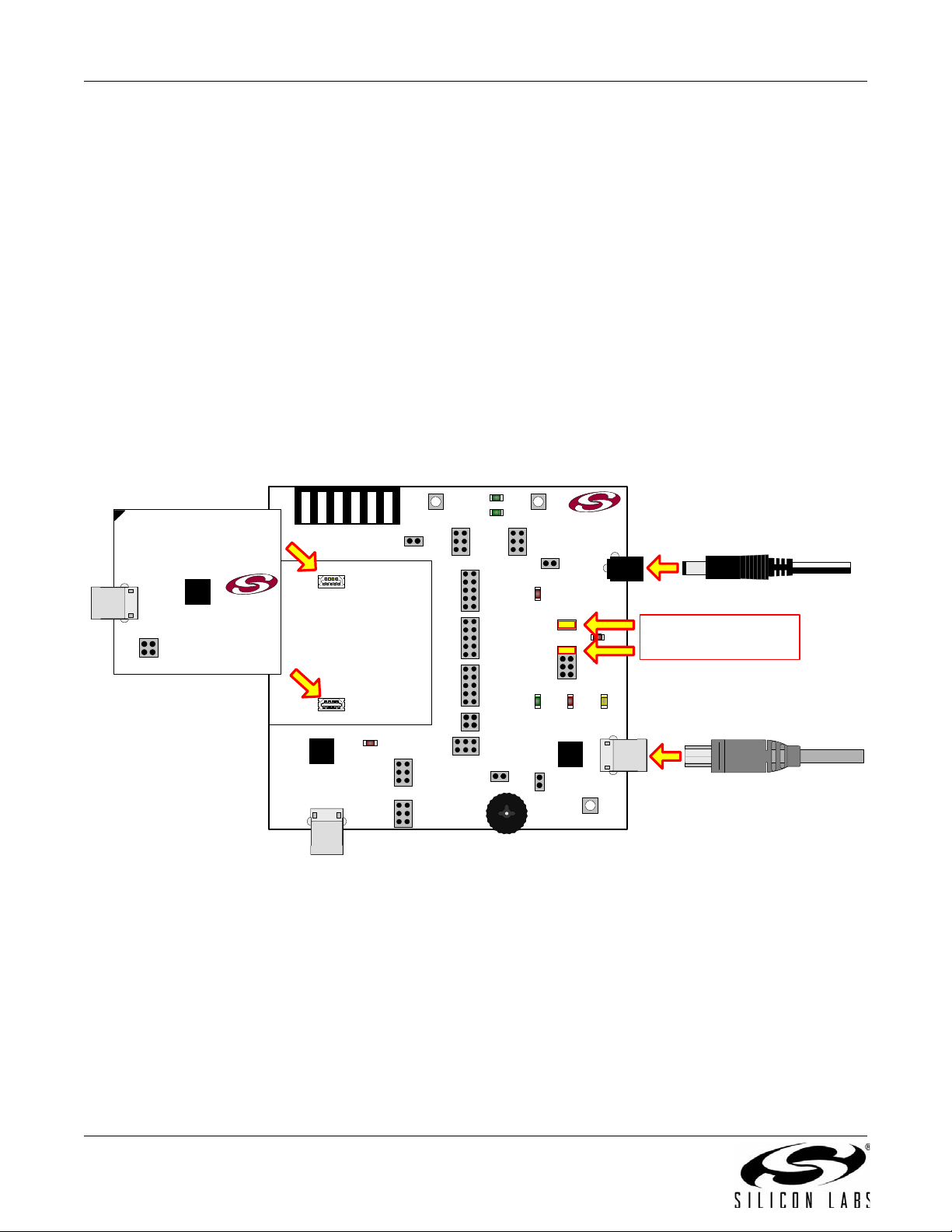
3. Hardware Setup
See Figure 1 for a diagram of the hardware configuration.
1. Attach the desired daughter board to the motherboard at connectors P1 and P2.
2. If using the QFN Socket Daughter Board, place the device to be programmed into the socket.
3. Place shorting blocks on J7 and the +3VD-VDD_PWR jum p er pair on J6, as shown in Figu re 1.
4. Connect the motherboard’s P5 USB connector to a PC running the Silicon Laboratories IDE using the USB
Cable.
5. Connect the ac-to-dc power adapter to connector P3 on the motherboard.
Notes:
1. Use the Reset icon in the IDE to reset the target when connected during a debug session.
2. Remove power from the motherboard and remove the USB cable before removing a daughter board from the
motherboard. Connecting or disconnecting a daughter board when the power adapter or USB cable are connected can
damage the motherboard, the daughter board, or the socketed devic e.
3. Remove power from the motherboard and remove the USB cable before removing a C8051T62x/32x device from the
socket. Inserting or removing a device from the socket when the power adapter or USB cable are connected can
damage the motherboard, the daughter board, or the socketed devic e.
4. The above hardware setup instructions configure the development system to be powered through the onboard 3.3 V
regulator. For other power options, see "7.3. Power Supply Headers (J6 and J7)" on page 14.
2 Rev. 0.4
Figure 1. Hardware Setup (Emulation Daughter Board)
Page 3

C8051T620/2-DK
4. Software Installation
The included CD-ROM contains the Silicon Laboratories Integrated Development Environment (IDE), 8051
evaluation toolset, Virtual COM Port drivers for the CP210x USB to UART Bridge, and additional documentation.
Insert the CD-ROM into your PC's CD-ROM drive. An installer will automatically launch, allowing you to install the
IDE software or read documentation by clicking buttons on the installation panel. If the installer does not
automatically start when you insert the CD-ROM, run autorun.exe, which is found in the root directory of the CD-
ROM. Refer to the ReleaseNotes.txt file on the CD-ROM for the latest information regarding the CD contents.
4.1. System Requirements
The following are the system requirements necessary to run the debug and programming tools:
Pentium-class host PC running Microsoft Windows 2000 or newer.
One available USB port.
4.2. Development Tools Installation
To install the IDE, utilities, and code examples, perform the following steps:
1. Click on the “Install Development Tools” button on the installation utility's startup screen.
2. In the Kit Selection box that appears, choose the C8051T620-DK or C8051T622-DK development kit from the
list of options.
3. In the next screen, choose “Components to be Installed”. The programs necessary to download and debug on
the MCU are the Silicon Labs IDE and the 8051 Evaluation Toolset. The CP210x Drivers are necessary to use
the UART capabilities of the target board. See “4.3. CP210x USB to UART VCP Driver Installation” for more
information about installing the CP210x drivers. See “5. Software Overview” for an overview of all applicable
software included on the CD-ROM.
4. Installers selected in Step 3 will execute in sequence, prompting the user as they install programs,
documentation, and drivers.
4.3. CP210x USB to UART VCP Driver Installation
The C8051T62x Motherboard includes a Silicon Laboratories CP2103 USB-to-UART Bridge Controller. Device
drivers for the CP2103 need to be installed before PC software, such as HyperTerminal, can communicate with the
board over the USB connection. If the “Install CP210x Drivers” option was selected during installation, this will
launch a driver “unpacker” utility.
1. Follow the steps to copy the driver files to the desired location. The default di rectory is C:\SiLabs\MCU\CP210x.
2. The final window will give an option to install the driver on the target system. Select the “Launch the CP210x
VCP Driver Installer” option if you are ready to install the driver.
3. If selected, the driver installer will now launch, providing an option to specify the driver installation location. After
pressing the “Install” button, the installer will search your system for copies of previously installed CP210x
Virtual COM Port drivers. It will let you know when your system is up-to-date. The driver files included in this
installation have been certified by Microsoft.
4. If the “Launch the CP210x VCP Driver Installer” option was not selected in Step 3, the installer can be found in
the location specified in Step 2 (by default, C:\SiLabs\MCU\CP210x\Windows). At this location, run
CP210xVCPInstaller.exe.
5. To complete the installation process, connect the included USB cable between the host computer and the
COMM USB connector (P4) on the C8051T62x Motherboard. Windows will automatically finish the driver
installation. Information windows will pop up from the taskbar to show the installation progress.
6. If needed, the driver files can be uninstalled by selecting the “Silicon Laboratories CP210x USB to UART Bridge
(Driver Removal)” option in the “Add or Remove Programs” window.
Rev. 0.4 3
Page 4
C8051T620/2-DK
5. Software Overview
The following software is necessary to build a project, download code to, and communicate with the target
microcontroller.
8051 Evaluation Toolset
Silicon Labs Integrated Development Environment (IDE)
Other useful software that is provided on the development kit CD and the Silicon Labs Downloads website
( www.silabs.com/mcudownloads) includes:
Configuration Wizard 2
Keil µVision2, µVision3, and µVision4 Drivers
MCU Production Programmer and Flash Programming Utilities
5.1. 8051 Evaluation Toolset
The Silicon Labs IDE has native support for many third-party 8051 toolsets. Included with this kit is an 8051
evaluation assembler, compiler, and linker. For further information on the tools, including limitations, see the
corresponding application note. Application notes can be found in the documentation section of the Development
Kit CD or on the Silicon Labs web site (http://www.silabs.com/appnotes) . See Table 1 for a list of supported toolsets
and associated application notes.
Table 1. Supported Third Party 8051 Toolsets
Toolset Application Note
Keil “AN104: Integrating Keil 8051 Tools into the Silicon Labs IDE”
Raisonance “AN125: Integrating Raisonance 8051 Tools into the Silicon Labs IDE”
Tasking “AN126: Integrating Tasking 8051 Tools into the Silicon Labs IDE”
HI-TECH “AN140: Integrating Hi-TECH 8051 Tools into the Silicon Labs IDE”
SDCC “AN198: Integrating SDCC 8051 Tools into the Silicon Labs IDE”
IAR “AN236: Integrating IAR 8051 Tools into the Silicon Labs IDE”
5.2. Silicon Labs IDE
The Silicon Labs IDE integrates a source-code editor, source-level debugger, and in-system programmer. The
following sections discuss how to open an example project in the IDE, build the source code, and download it to the
target device.
5.2.1. Running the T620_Blinky or T622_Blinky example program
The T620_Blinky or T622_Blinky example program blinks an LED on the target board.
1. Open the Silicon Labs IDE from the Start menu.
2. Select Project
3. Browse to the C:\SiLabs\MCU\Examples\C8051T620_1_T320_3\Blinky or SiLabs\MCU\Exam-
ples\C8051T622_3_T326_7\Blinky directory (default) and select the T620_Blinky_C.wsp pr
T622_Blinky_C.wsp project file. Click Open.
4. Once the project is open, build the project by clicking on the Build/Make Project button in the toolb ar or
selecting Project
Note: After the project has been built the first time, the Build/Make Project command will only build the
files that have been changed since the previous build. To rebuild all files and project dependencies, click
on the Rebuild All button in the toolbar or select Project
5. Before connecting to the target device, several connection optio ns may need to be set. Open th e Connec-
tion Options window by selecting Options
“USB Debug Adapter” option. Next, the correct “Debug Interface” must be selected. C8051T62x/32x
devices use Silicon Labs “C2” 2-wire debug interface. Once all the selections are made, click the OK button to close the window.
Open Project to open an existing project.
Build/Make Project from the menu.
Rebuild All from the menu.
Connection Options... in the IDE menu. First, select the
4 Rev. 0.4
Page 5
C8051T620/2-DK
6. Click the Connect button in the toolbar or select DebugConnect from the menu to connect to the
device.
7. Download the project to the target by clicking the Download Code button in the toolbar.
Note: To enable automatic downloading if the program build is successful, select Enable Automatic Con-
nect/Download after Build in the Project
build process, the IDE will not attempt the download.
8. Click on the Go button (green circle) in the toolbar or by selecting Debug
ning the firmware. The LED on the target board will start blinking.
5.2.2. Creating a New Project
Use the following steps to create a new projec t. Once ste ps 1–5 in this se ction are co mplete, c ontinue with Step 3
from Section 5.2.1.
1. Select Project
2. Select File
ognized extension, such as .c, .h, or .asm, to enable color syntax highlighting.
3. Right-click on “New Project” in the Project Window. Select Add files to project. Select files in the file
browser and click Open. Continue adding files until all project files have been added.
4. For each of the files in the Project Window that you want assembled, compiled, and linked into the target
build, right-click on the file name and select Add file to build. Each file will be assembled or compiled as
appropriate (based on file extension) and linked into the build of the absolute object file.
Note: If a project contains a large number of files, the “Group” feature of the IDE can be used to organize.
Right-click on “New Project” in the Project Window. Select Add Groups to project. Add predefined groups
or add customized groups. Right-click on the grou p name and cho ose Add file to group. Select files to be
added. Continue adding files until all project files have been added.
5. Save the project when finished with the debug session to preserve the current target build configuration,
editor settings, and the location of all open debug views. To save the project, select Project
ect As... from the menu. Create a new name for the project and click on Save.
New Project to open a new project and reset all configuration settings to default.
New File to open an editor window. Create your source file(s) and save the file(s) with a rec-
T arget Build Configurat ion dialog. If errors occur during the
Go from the menu to start run-
Save Proj-
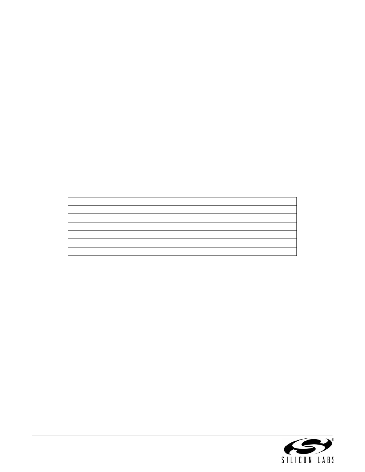
5.3. Configuration Wizard 2
Configuration Wizard 2 is a code generation tool for all Silicon Laboratories devices. Code is generated through the
use of dialog boxes for each device peripheral as shown in Figure 2.
Figure 2. Configuration Wizard 2 Utility
Rev. 0.4 5
Page 6

C8051T620/2-DK
The Configuration Wizard utility helps accelerate development by automatically generating initialization source
code to configure and enable the on-chip resour ces needed b y most design project s. In just a few steps, th e wizard
creates complete startup code for a specific Silicon Laboratories MCU. The program is configurable to provide the
output in C or assembly language.
For more information, refer to the Configuration Wizard 2 help available under the Help menu in Configuration
Wizard 2 or refer to the Configuration Wizard 2 documentation. Documentation and software are available on the
kit CD and from the downloads webpage: www.silabs.com/mcudownloads.
5.4. Keil uVision2, uVision3, and uV ision4 Silicon La boratories Drivers
As an alternative to the Silicon Laboratories IDE, the µVision debug driver allows the Keil µVision2, µVision3, and
µVision4 IDEs to communicate with Silicon Laboratories’ on-chip debug logic. In-system Flash memory
programming integrated into the driver allows for rapid updating of target code. The µVision2, µVision3, and
µVision4 IDEs can be used to start and stop program execution, set breakpoints, check variables, inspect and
modify memory contents, and single-step through programs running on the actual target hardware.
For more information, refer to the µVision driver documentation. The documentation and software are available on
the kit CD and from the downloads webpage: www.silabs.com/mcudownloads.
5.5. Programming Utilities
The Silicon Labs IDE is the primary tool for downloading firmware to the MCU during development. There are two
software programming tools that are intended for use during prototyping or in the field: the MCU Production
Programmer and the Flash Programming Uti lities. The MCU Production Pro grammer is inst alled with the IDE to the
directory, C:\Silabs\MCU\Utilities\Production Programmer\ (default). The Flash Programming Utilities can be
optionally installed from the CD and are installed to C:\Silabs\MCU\Utilities\FLASH Programming\ (default).
5.6. ToolStick Terminal
The onboard debug circuitry provides both an in-system programming and debugging interface and a
communications interface to the target microcontroller's UART. The ToolStick Terminal software can access the
debug hardware's communications path and provides a terminal-like interface on the PC. Note that for concurrent
debugging and UART communications, the CP2103 USB-to-UART bridge is also included onboard.
In addition to the standard terminal functions (Send File, Receive File, Change Baud Rate), two GPIO pins on the
target microcontroller can be controlled using the terminal for either RTS/CTS handshaking or softwareconfigurable purposes. The ToolStick Terminal software is available on the downloads webpage: www.silabs.com/
mcudownloads.
6 Rev. 0.4
Page 7

C8051T620/2-DK
6. Example Source Code
Example source code and register definition files are provided by default in the
SiLabs\MCU\Examples\C8051T620_1_T320_3 or SiLabs\MCU\Examples\C8051T622_3_T326_7 directory during
IDE installation. These files may be used as a template for code development.
6.1. Register Definition Files
Register definition files C8051T620.inc, C8051T622.inc, C8051T620_defs.h, C8051T622_defs.h, and
compiler_defs.h define all SFR registers and bit-addressable control/status bits. They are installed by default into
the SiLabs\MCU\Examples\C8051T620_1_T320_3 or SiLabs\MCU\Examples\C8051T622_3_T326_7 directory
during IDE installation. The register and bit names are identical to those used in the C8051T620-21_T320-3 or
C8051T620-23_T326-27 dat a sheet.
6.2. Blinking LED Example
The example source files T620_Blinky.asm and T620_Blinky.c or T622_Blinky.asm and T622_Blinky.c show
examples of several basic C 8051T62x functions. Thes e include disabling the watchdog timer (WDT), c onfiguring
the Port I/O crossbar, configuring a timer for an interrupt routine, initializing the system clock, and configuring a
GPIO port. When compiled/assembled and linked, these programs flash the green LED on the C8051T62x
Motherboard about five times a second using the interrupt handler with a timer.
Rev. 0.4 7
Page 8

C8051T620/2-DK
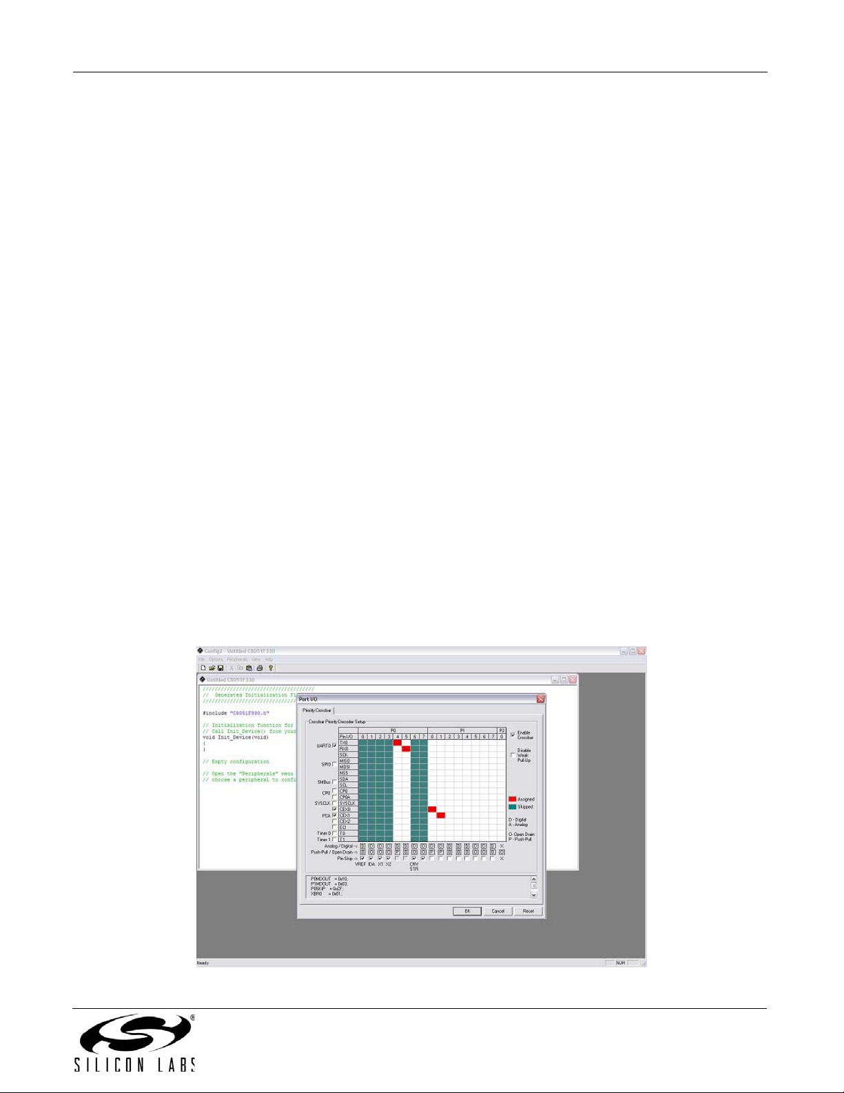
7. Development Boards
The C8051T620/2 Development Kit includes a motherboard that interfaces to various daughter boards. The
C8051T62x Emulation Daughter Board contains a C8051F34A device to be used for preliminary software
development. The C8051T620 Socket Daughter Board and C8051T622 Socket Daughter Board allow
programming and evaluation of the actual C8051T62x devices. Numerous input/output (I/O) connections are
provided on the motherboard to facilitate prototyping. Figure 3 shows the C8051T62x Motherboard and indicates
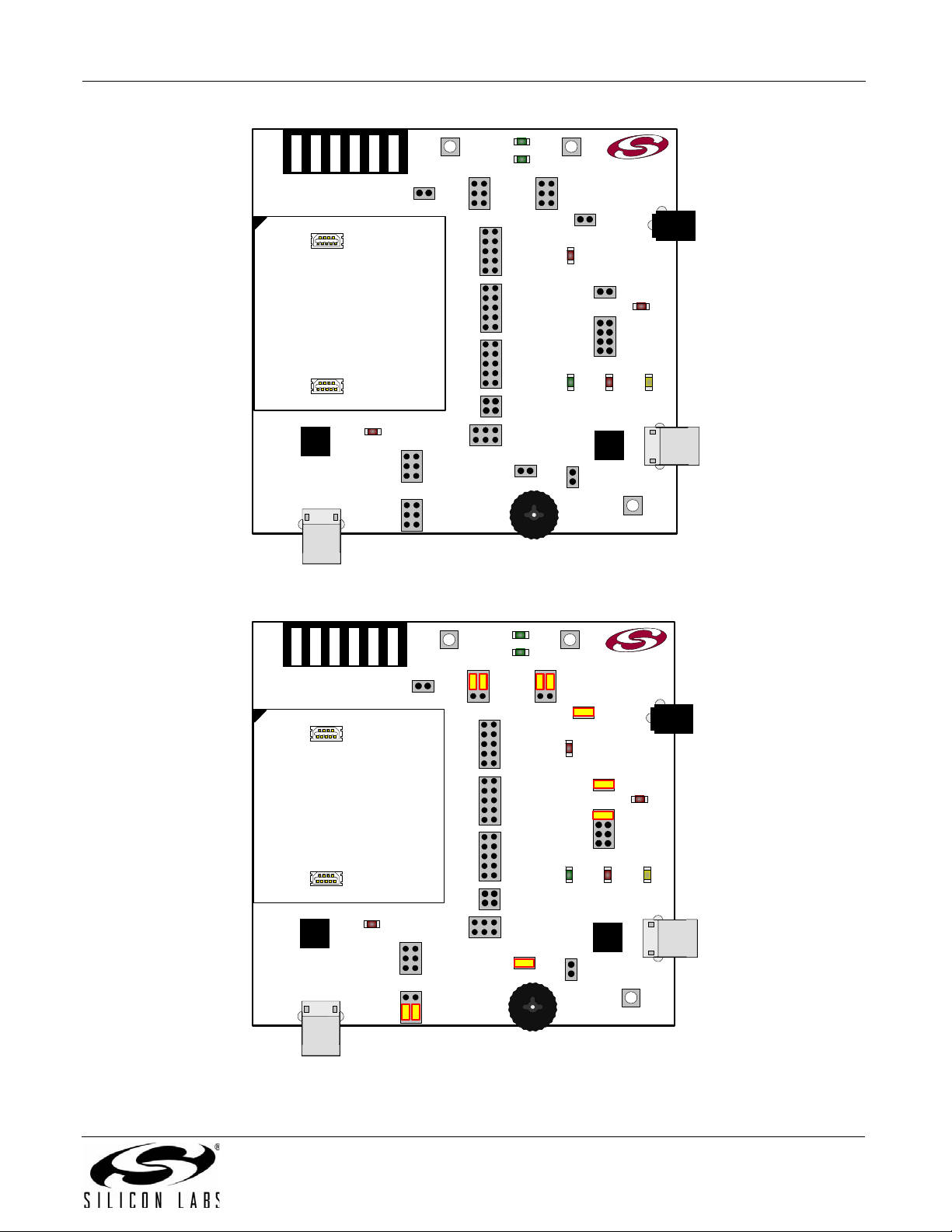
locations for various I/O connec tors. Figure 4 shows the factory default shorting block positions. Figures 5, 6, and 7
show the available C8051T62x daughter boards. Figures 8, 9, 10, and 11 show the available C8051T32x daughter
boards.
P1, P2 Daughter board connection
P3 Power connector that accepts input from 7.5 to 15 V dc unregulated power adapter
P4 USB connector for UART to USB communications interface
P5 USB Debug interface connector
J1 Analog I/O terminal block
J2 Port 0 header
J3 Port 1 header
J4 Port 2 header
J5 Port 3 header with access to VDD and GND
J6 Power supply selection header (See "7.3. Power Supply Headers (J6 and J7)" on page 14)
J7 Power supply enable header that connects power source selecte d on J6 to the board's main
power supply net
J8 Communications interface control signal header
J9 Connects port pins to the switches labeled “SW1” and “SW2”
J10 Connects port pins to the LEDs labeled “LED1” and “LED2”
J11 Communications interface data signal header
J12 Connects potentiometer to the port pin, P2.5
J13 Additional connections to ground
J14 Connects an external VREF from J1 to P0.7
J15 VPP supply connection used when programming EPROM devices
8 Rev. 0.4
Page 9
C8051T620/2-DK
P3
SILICON LABS
www.silabs.com
RESET
J15
J7
USB ACTIVE
J5
J14
SW1
J12
J13
J1
DEBUG
PWR
RUN
VDD_PWR
VDD_PWR
VDD_PWR
VDD_PWR
+3VD
VDD_EXT
VDD_DEBUG
VDD_COMM
J6
P2
P1
J2
SW2
J3
J4
USB ACTIVE
LED1
PWR
D10
D11 D12
R8
U2
CP2103
U1
F326
STOP
LED1
J10
P2.2
P0.6
LED2
P2.3
P1.2
SW1
J9
P2.0
P0.1
SW2
P2.1
P1.0
C8051T62x-MB
LED2
VPP
P5
P4
J8
CTS_DEBUG
P1.1 P1.2
RTS_COMM CTS_COMM
RTS_DEBUG
J11
TX_DEBUG
P0.4 P0.5
RX_COMM TX_COMM
RX_DEBUG
Figure 3. C8051T62x Motherboard
Figure 4. C8051T62x Motherboard Default Shorting Block Positions
Rev. 0.4 9
Page 10

C8051T620/2-DK
U1
F34A
VREGIN
VREGIN
VBUS
VDD
P3
SILICON LABS
www.silabs.com
C8051T62x EDB
J1
VBUS
VREGIN
VDD
VREGIN
P3
VIO
VDD
J2
C8051T62x QFN32 SKT DB
SILICON LABS
www.silabs.com
J3
J1
VBUS
VREGIN
VDD
VREGIN
SILICON LABS
www.silabs.com
P3
VIO
VDD
J2
C8051T622 QFN24 SKT DB
J3
Figure 5. C8051T62x Emulation Daughter Board
Figure 6. C8051T620 QFN32 Socket Daughter Board
Figure 7. C8051T622 QFN24 Socket Daughter Board
10 Rev. 0.4
Page 11

C8051T620/2-DK
J1
VBUS
VREGIN
VDD
VREGIN
SILICON LABS
www.silabs.com
P3
J2
C8051T320 QFP32 SK T DB
J1
VBUS
VREGIN
VDD
VREGIN
SILICON LABS
www.silabs.com
P3
J2
C8051T321 QFN28 SKT DB
J1
VBUS
VREGIN
VDD
VREGIN
SILICON LABS
www.silabs.com
P3
VIO
VDD
J2
C8051T326 QFN28 SKT DB
J3
Figure 8. C8051T320 QFP32 Socket Daughter Board
Figure 9. C8051T321 QFN28 Socket Daughter Board
Figure 10. C8051T326 QFN28 Socket Daughter Board
Rev. 0.4 11
Page 12

C8051T620/2-DK
J1
VBUS
VREGIN
VDD
VREGIN
SILICON LABS
www.silabs.com
P3
C8051T327 QFN28 SKT DB
J3
Figure 11. C8051T327 QFN28 Socket Daughter Board
12 Rev. 0.4
Page 13

C8051T620/2-DK
7.1. System Clock Sources
The C8051T62x/32x devices feature a calibrated internal oscillator that is enabled as the system clock source on
reset. After reset, the internal oscillator operates at a frequency of 48 MHz (±1.5%) by default but may be
configured by software to operate at other frequencies. Therefore, in many applications, an external oscillator is not
required. However, if you wish to operate the C8051T62x/32x device at a frequency not available with the internal
oscillator, an external oscillator source may be used. Refer to the C8051T620-21_T320-3 or C8051T620-23_T32627 data sheet for more information on configuring the system clock source.
7.2. Switches, LEDs, and Potentiometer (J9, J10, and J12)
Three switches are provided on the motherboard. The RESET switch is connected to the RST pin of the
C8051T62x/32x. Pressing RESET puts the device into its hardware-reset state. The switch labeled “SW1” can be
connected to the C8051T62x/32x's general-purpose I/O (GPIO) pins P0.1 and P2.0, and “SW2” can be connected
to the C8051T62x/32x's general-purpose I/O (GPIO) pins P1.0 and P2.1 through header J9. Pressing a switch
generates a logic low signal on the port pin. Rem ove its shorting block from the J9 header to disconnect the switch
from the port pin.
Seven LEDs are also provided on the motherboard. The red LED labeled “PWR” (D4) is used to indicate a power
connection to the motherboard. The green LED labeled “RUN” (D10) turns on when the debug circuitry is in a
running state; the red LED labeled “STOP” (D11) turns on when the debug circuitry is in a halted state, and the
orange LED labeled “DEBUG PWR” (D12) indicates whether the debug adapter circuit is being powered through
P5's USB connector. The red LED labeled “VPP” (D7) indicates when the VPP programming voltage is being
applied to the device. The green LEDs, labeled “LED1” (D1) and “LED2” (D2), can be connected to C8051T62x/
32x's GPIO pins through header J10. Remove its shorting block from the header to disconnect an LED from the
port pin. The red LED labeled “USB ACTIVE” (D13) will turn on whenever the CP2103 USB-to-UART bridge is
connected to a PC and has successfully complete d en um e ratio n.
Also included on the C8051T62x Motherboard is a 10 k thumbwheel rotary potentiometer, reference number R8.
The potentiometer can be connected to the C8051T62x/32x's P2.5 pin through the J12 header. Remove the
shorting block from the header to disconnect the potentiometer from the port pin.
Rev. 0.4 13
Page 14

C8051T620/2-DK
J7
J6
VDD_PWR
+3VD
VDD_EXT
VDD_DEBUG
VDD_COMM
J7
J6
VDD_PWR
+3VD
VDD_EXT
VDD_DEBUG
VDD_COMM
J7
J6
VDD_PWR
+3VD
VDD_EXT
VDD_DEBUG
VDD_COMM
J7
J6
VDD_PWR
+3VD
VDD_EXT
VDD_DEBUG
VDD_COMM
+3.3V Regulator Power
(From P3)
CP2103 Regulator Power
(From USB at P4)
Debug Circuit Power
(From USB at P5)
External Power Source
(From J1 Connector)
VDD_PWR VDD_PWRVDD_PWRVDD_PWRVDD_T620 VDD_T620 VDD_T620 VDD_T620
Table 2 lists the port pins and headers corresponding to the switches, LEDs, and potentiometer.
Table 2. Motherboard I/O Descriptions
Description Component Name I/O Header
Switch SW1 Daughter Card's P0.1
Daughter Card’s P2.0
Switch SW2 Daughter Card’s P1.0
Daughter Card’s P2.1
J9 [2-4]
J9 [4-6]
J9 [1-3]
J9 [3-5]
RESET SW3 Daughter Card's RST/C2CK None
Green LED labeled “LED1” D1 Daughter Card's P0.6
Daughter Card's P2.2
Green LED labeled “LED2” D2 Daughter Card’s P1.2
Daughter Card's P2.3
J10 [2-4]
J10 [4-6]
J10 [1-3]
J10 [3-5]
Red LED labeled “PWR” D4 Daughter Card's VDD J6, J7
Red LED labeled “VPP” D7 Daughter Card's VPP pin
J15
(See "VPP Pin Sharing" on
page 16)
Green LED labeled “RUN” D10 Debug Adapter Signal None
Red LED labeled “STOP” D11 Debug Adapter Signal None
Orange LED labeled “DEBUG PWR” D12 Debug Adapter Signal None
Green LED labeled “USB ACTIVE” D13 U2 CP2103's SUSPEND None
Potentiometer R8 Daughter Card's P2.5 J12
7.3. Power Supply Headers (J6 and J7)
The main power supply of the motherboard, which is used to power the daughter board, can be provided by either
the USB Debug Adapter’s on-chip voltage regulator, the CP2103 USB-to-UART bridge’s on-chip voltage regulator,
P3 and its associated circuitry, or an external voltage applied to the VDD_EXT connection on J1. To select a power
supply, place a shorting block on J6 across the appropriate pin pair, as shown in Figure 12. To connect the main
power supply to an attached daughter board, place a shorting block across J7.
Notes:
1. Only one shorting block should be placed on J6 at a time.
2. To use the CP2103’s voltage regulator as the board's power supply, a USB cable must be connected to P4, and the USB
ACTIVE LED (D2) must be on.
3. To use the USB Debug Adapter’s voltage regulator as the board's power supply, a USB cable must be connected to P5,
and the DEBUG PWR LED (D12) must be on.
14 Rev. 0.4
Figure 12. J6 and J7 Shorting Block Configuration for Power Options
Page 15

C8051T620/2-DK
CTS_DEBUG
P1.1 P1.2
RTS_COMM CTS_COMM
RTS_DEBUG
J8
CTS_DEBUG
P0.4 P0.5
RX_COMM CTS_COMM
RX_DEBUG
J11
CP2103 Bridge
(USB Connection at P4)
RTS_DEBUG
P1.1 P1.2
RTS_COMM CTS_COMM
RTS_DEBUG
J8
TX_DEBUG
P0.4 P0.5
RX_COMM TX_COMM
RX_DEBUG
J11
Debug Adapter Comms
(USB Connection at P5)
7.4. USB Debug Adapter (DEBUG/P5)
A Universal Serial Bus (USB) connector (P5) provides the onboard debug and programming interface. The debug/
programming MCU and ass ociated circuitry are powered th rough the USB connector, which can also supply the
rest of the motherboard by routing the USB Debug Adapter's power through J6. The USB Debug Adapter also
provides a data communications interface that can be used when the debug adapter is not debugging or
programming a C8051T62x/32x device.
7.5. UART to USB Communications Interfaces (COMM/P4)
The C8051T62x Motherboard provides UART to USB communications interfaces through both the CP2103 USBto-UART bridge device and the communications interface of the USB Debug Adapter.
The CP2103 bridge device connects to a PC through the USB connector labeled “COMM” (P4). This USB
connector supplies power to the CP2103 and can supply power to the rest of the motherboard by configuring J6
and J7 as shown in Figure 12. To use the CP2103 as a communications interface, the CP2103 Virtual COM Port
drivers must be installed on a PC.
The USB Debug Adapter's communications interface connects to a PC through P5. Access to the USB Debug
Adapter's communications interface is provided by the Windows program called “ToolStick Terminal”, which is
available for download for free from the Silicon Laboratories website. See the ToolStick Terminal help file for
information on how to use ToolStick Terminal.
7.6. Communications Interface Selector Headers (J8 and J11)
The C8051T62x Motherboard routes the C8051T62x/32x's P0.4 (UART TX) and P0.5 (UART RX) to J11 where
those signals can be connected to either the CP2103 USB-To-UART bridge or the USB Debug Adapter. The
motherboard also allows the C8051T62x/32x's P1.1 and P1.2 to be used as the UART control signals, CTS and
RTS. These two signals are routed to J8, where they can be connected to either the CP2103 or the USB Debug
Adapter.
The jumper options for using either the CP2103 or the Debug Adapter circuit for UART communications can be
found in Figure 13.
7.7. PORT I/O Connectors (J2, J3, J4, and J5)
Each of the C8051T62x/32x's I/O pins, as well as +3VD and GND, are routed to headers J2 through J5. J2
connects to the microcontroller's Port 0 pins; J3 connects to Port 1; J4 connects to Port 2, and J5 connects to
Port 3.
Figure 13. Shorting Block Configuration for UART Communication Options
Rev. 0.4 15
Page 16

C8051T620/2-DK
7.8. Analog I/O (J1 and J14)
Three of the C8051T62x/32x target device's port pins are connected to the J1 terminal block. The terminal block
also allows users to input an external voltage that can be used as the power supply of the board. Refer to Table 3
for the J1 terminal block connections. Placing a shorting block on J14 will connect the P0.7/VREF signal on J1 to
the P0.7 pin of the device.
Table 3. J1 Terminal Block Descriptions
Pin # Description
1VREGIN
2VIO
3GND
4 P2.5 (Analog Input)
5 P0.7/VREF (routed to header J14)
6 VDD_EXT (routed to header J6)
7.9. VPP Connection (J15)
The C8051T62x/32x devices require an external 6.0 V programming voltage applied to the VPP pin during device
programming. The VPP pin on these devices is shared with P1.5 or P1.1 depending on the device. During
programming, the VPP voltage is automatically enabled when needed. Header J15 is provided to allow the user to
disconnect the programming circuitry from the VPP pin to avoid interfering with the normal application operation of
the GPIO pin. When programming the device, J15 should be shorted with a shorting block. When running normal
application code, J15 can be removed. See Table 4 for more information on which port pins are shared with VPP.
Table 4. VPP Pin Sharing
Device Pin Shared with VPP
C8051T620
C8051T621
C8051T320
C8051T321
C8051T322
C8051T323
C8051T622
C8051T623
C8051T326
C8051T327
P1.5
P1.1
16 Rev. 0.4
Page 17

C8051T620/2-DK
7.10. Using Alternate Supplies with the C8051T62x Development Kit
For most evaluation purposes, the onboard 3.3 V supply regulator is sufficient to be used as a VDD power supply.
However, in application s where a dif ferent su pply volt age is desired ( e.g., 1.8 V), an external supply voltage can be
applied to the board at the analog connector (J1). Some devices in the C8051T62x/32x family also support a
separate voltage input for the input/output voltage of t he po rt pin s. T h is Voltage Input/Output (VIO) should be in pu t
to J1 on Pin 2. See the C8051T620-21_T320-3 or C8051T620-23_T326-27 data sheet for more information about
VIO usage and constraints.
Notes:
When programming a C8051T62x/32x device, VDD must be at least 3.3 V. VDD can be supplied directly to the
device, or the on-chip 5 V regulator can be used.
If an external supply voltage is desired, the shorting block on J6 should be placed so that th e Pin 3 ( VDD_EXT)
is shorted to Pin 4 (VDD_PWR).
Rev. 0.4 17
Page 18

C8051T620/2-DK
8. Schematics
18 Rev. 0.4
Figure 14. C8051T62x Motherboard Schematic (1 of 2)
Page 19

C8051T620/2-DK
Figure 15. C8051T62x Motherboard Schematic (2 of 2)
Rev. 0.4 19
Page 20

C8051T620/2-DK
20 Rev. 0.4
Figure 16. C8051T62x Emulation Daughter Board Schematic
Page 21

C8051T620/2-DK
Figure 17. C8051T620 QFN-32 Daughter Board Schematic
Rev. 0.4 21
Page 22

C8051T620/2-DK
22 Rev. 0.4
Figure 18. C8051T622 QFN-24 Daughter Board Schematic
Page 23

C8051T620/2-DK
Figure 19. C8051T320 QFP-32 Daughter Board Schematic
Rev. 0.4 23
Page 24

C8051T620/2-DK
24 Rev. 0.4
Figure 20. C8051T321 QFN-28 Daughter Board Schematic
Page 25

C8051T620/2-DK
Figure 21. C8051T326 QFN-28 Daughter Board Schematic
Rev. 0.4 25
Page 26

C8051T620/2-DK
26 Rev. 0.4
Figure 22. C8051T327 QFN-28 Daughter Board Schematic
Page 27

DOCUMENT CHANGE LIST
Revision 0.2 to Revision 0.3
Updated "4.2. Development Tools Installation" on
page 3.
Updated "4.3. CP210x USB to UART VCP Driver
Installation" on page 3.
Updated Fi gu re 17 on page 21.
Updated Fi gu re 18 on page 22.
Updated Figure on page 27.
Revision 0.3 to Revision 0.4
Updated "1. Kit Contents" on page 1.
Updated "2. About the Daughter Boards" on page 1.
Updated "6. Example Source Code" on page 7.
Updated project paths
Updated "7. Deve lo pm e nt Bo ar ds " on page 8.
Updated "8. Sc hem atics" on page 18.
Added Figures 19, 20, 21, and 22.
Updated C8051T62x references to include
C8051T32x devices.
Updated data sheet re fe re nc es .
C8051T620/2-DK
Rev. 0.4 27
Page 28

C8051T620/2-DK
The information in this document is believed to be accurate in all respects at the time of publication but is subject to change without notice.
Silicon Laboratories assumes no responsibility for errors and omissions, and disclaims responsibility for any consequences resulting from
the use of information included herein. Additionally, Silicon Laboratories assumes no responsibility for the functioning of undescribed features
or parameters. Silicon Laboratories reserves the right to make changes without further notice. Silicon Laboratories makes no warranty, representation or guarantee regarding the suitability of its products for any particular purpose, nor does Silicon Laboratories assume any liability
arising out of the application or use of any product or circuit, and specifically disclaims any and all liability, including without limitation consequential or incidental damages. Silicon Laboratories products are not designed, intended, or authorized for use in applications intended to
support or sustain life, or for any other application in which the failure of the Silicon Laboratories product could create a situation where personal injury or death may occur. Should Buyer purchase or use Silicon Laboratories products for any such unintended or unauthorized application, Buyer shall indemnify and hold Silicon Laboratories harmless against all claims and damages.
CONTACT INFORMATION
Silicon Laboratories Inc.
400 West Cesar Chavez
Austin, TX 78701
Tel: 1+(512) 416-8500
Fax: 1+(512) 416-9669
Toll Free: 1+(877) 444-3032
Please visit the Silicon Labs Technical Support web page:
https://www.silabs.com/support/pages/contacttechnicalsupport.aspx
and register to submit a technical support request.
Silicon Laboratories and Silicon Labs are trademarks of Silicon Laboratories Inc.
Other products or brandnames mentioned herein are trademarks or registered trademarks of their respective holders.
28 Rev. 0.4
 Loading...