

Page 1
C8051F96x/Si102x
UDP C8051F960/Si1020 MCU CARD WITH EMIF
U
SER’S GUIDE
1. Introduction
The Unified Development Platform (UDP) provides a development and demonstration platform for Silicon
Laboratories microcontrollers and the Silicon Laboratories software tools, including the Silicon Laboratories
Integrated Development Environment (IDE).
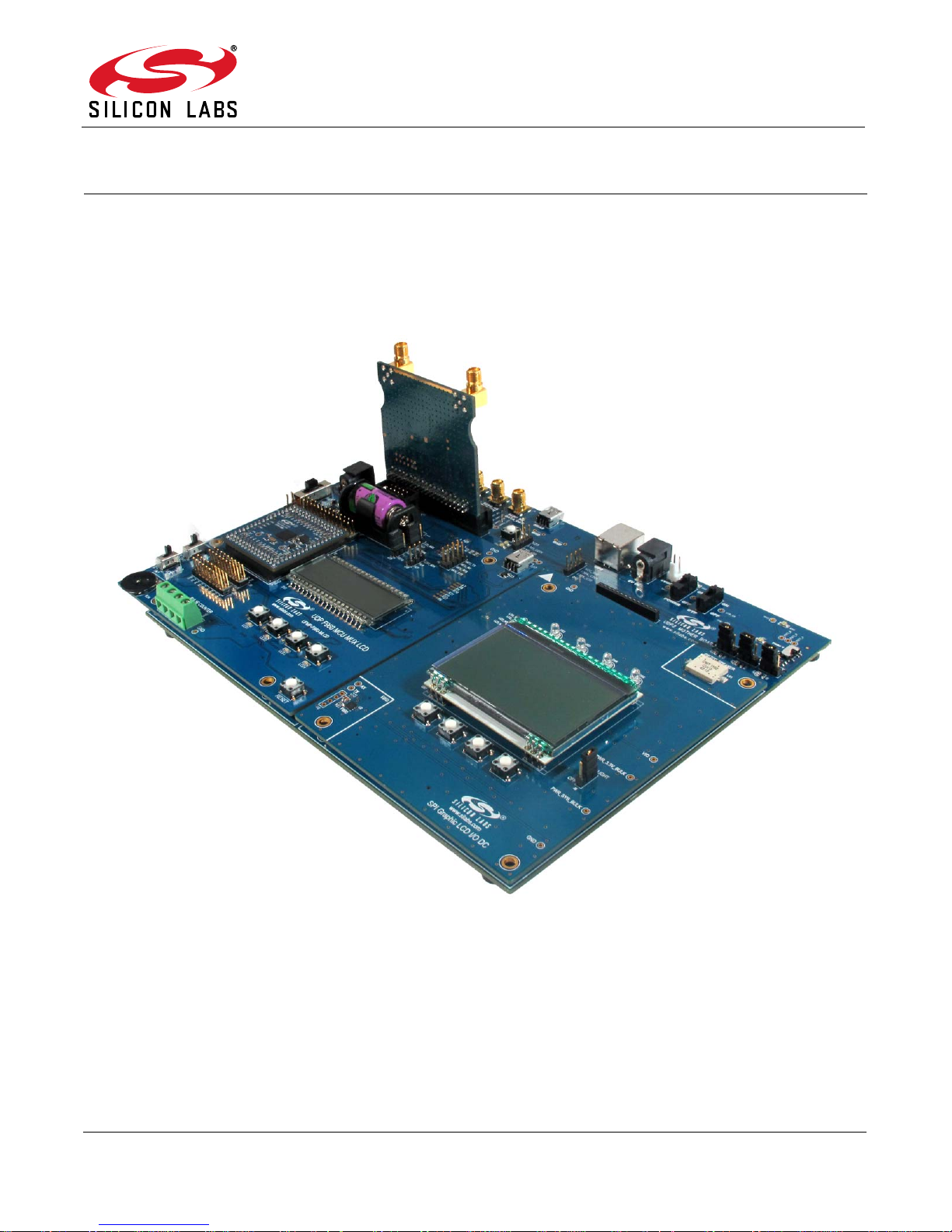
Figure 1. Unified Development Platform
Rev. 0.2 2/14 Copyright © 2014 by Silicon Laboratories C8051F96x
Page 2

C8051F96x/Si102x
2. Relevant Documents
This document provides a hardware overview for the Unified Development Platform (UDP) system UDP
C8051F960/Si1020 MCU Card with EMIF. Additional information on the UDP system can be found in the
documents listed in this section.
2.1. Motherboard User’s Guide
The UDP Motherboard User’s Guide contains information on the motherboard features and can be found at
www.silabs.com.
2.2. Card User’s Guides
The UDP MCU Card and Radio Card User’s Guides can be found at www.silabs.com.
2 Rev. 0.2
Page 3

C8051F96x/Si102x
USB Debug Adapter
USB
Connectivity
Power
Adapter (P1)
VBAT
Switch
VIORF
Switch
VIO
Switch
3. Hardware Setup
3.1. Using the MCU Card Alone
Refer to Figure 2 for a diagram of the hardware configuration when using the MCU card without a UDP
motherboard.
1. Connect the USB Debug Adapter to the 2x5 debug connector on the MCU card with the 10-pin ribbon
cable.
2. Connect one end of the USB cable to the USB connector on the USB Debug Adapter.
3. Connect the other end of the USB cable to a USB Port on the PC.
4. Move the SW5 VBAT switch to the middle VREG position.
5. Move the SW7 VIO switch to the upper VBAT position.
6. Move the SW12 VIORF switch to the upper VBAT position.
7. Connect the 9 V DC adapter to P1.
Notes:
Use the Reset button in the IDE to reset the target when connected using a USB Debug Adapter.
Remove power from the MCU card and the USB Debug Adapter before connecting or disconnecting the
ribbon cable from the MCU card. Connecting or disconnecting the cable when the devices have powe r can
damage the device and/or the USB Debug Adapter.
Figure 2. Hardware Setup Using the MCU Card Alone
Rev. 0.2 3
Page 4
C8051F96x/Si102x
USB Debug Adapter
Power
Adapter
(J20)
USB
Connector
(J16)
VBAT
Switch
3.2. Using the MCU Card with the UDP Motherboard
Refer to Figure 3 for a diagram of the hardware configuration when using the MCU card with a UDP motherboard.
1. Connect the MCU card to the UDP motherboard slot.
2. (Optional) Connect the I/O card to the UDP motherboard slot.
3. (Optional) Connect a radio card to the radio card slot in the UDP motherboard.
4. (Optional) Connect an EZLink card to the EZLink card slot in the UDP motherboard.
5. Connect the USB Debug Adapter to the 2x5 debug connector on the MCU card with the 10-pin ribbon
cable.
6. Connect one end of the USB cable to the USB connector on the USB Debug Adapter.
7. Connect the other end of the USB cable to a USB Port on the PC.
8. Connect the ac/dc power adapter to power jack J20 on the UDP motherboard. The board can also be
powered from the J16 USB or J1 mini USB connectors.
9. Move the SW5 VBAT switch on the MCU card to the VREG position.
10. Move the SW7 VIO switch on the MCU card to the upper VBAT position.
11. Move the SW12 VIORF switch on the MCU card to the upper VBAT position.
12. Move the S3 power switch on the UDP motherboard to the ON position.
Notes:
Use the Reset button in the IDE to reset the target when connected using a USB Debug Adapter.
Remove power from the target boa rd and the USB De bug Adapter before connecting or disconnecting the
ribbon cable from the target board. Connecting or disconnecting the cable when the devices have power
can damage the device and/or the USB Debug Adapter.
Th e MCU card can be used alone without th e motherboard . However, the motherboard must be power ed if
an MCU card is connected.
Figure 3. Hardware Setup Using the Unified Development Platform
4 Rev. 0.2
Page 5

C8051F96x/Si102x
4. Software Setup
Simplicity Studio greatly reduces development time and complexity with Silicon Labs EFM32 and 8051 MCU
products by providing a high-powered IDE, tools for hardware configuration, and links to helpful resources, all in
one place.
Once Simplicity Studio is installed, the application itself can be used to install additional software and
documentation components to aid in the development and evaluation process.
The following Simplicity Studio components are required for the C8051F960 Development Kit:
8051 Products Part Support
Simplicity Developer Platform
Download and install Simplicity Studio from www.silabs.com/8bit-software or www.silabs.com/simplicity-studio.
Once installed, run Simplicity Studio by selecting St art
from the start menu or clicking the Simplicity Studio shortcut on the desktop. Follow the instructions to install the
software and click Simplicity IDE to launch the IDE.
The first time the project creation wizard runs, the Setup Environment wizard will guide the user through the
process of configuring the build tools and SDK selection.
In the Part Selection step of the wizard, select from the list of installed parts only the parts to use during
development. Choosing parts and families in this step affects the displayed or filtered parts in the later device
selection menus. Choose the C8051F96x family by checking the C8051F96x check box. Modify the part selection
at any time by accessing the Part Management dialog from the Window
Studio
Simplicity Studio can detect if certain toolchains are not activated. If the Licensing Helper is displayed after
completing the Setup Environment wizard, follow the instructions to activate the toolchain.
Part Management menu item.
Figure 4. Simplicity Studio
Silicon LabsSimplicity StudioSimplicity Studio
PreferencesSimplicity
Rev. 0.2 5
Page 6
C8051F96x/Si102x
4.1. Running Blinky
Each project has its own source files, target configuration, SDK configuration, and build configurations such as the
Debug and Release build configurations. The IDE can be used to manage multiple projects in a collection called a
workspace. Workspace settings are applied globally to all projects within the workspace. This can include settings
such as key bindings, window preferences, and code style and formatting options. Project actions, such as build
and debug are context sensitive. For example, the user must select a project in the Project Explorer view in order
to build that project.
To create a project based on the Blinky example:
1. Click the Simplicity IDE tile from the Simplicity Studio home screen.
2. Click the Create new project link from the welcome screen or go to File
Project.
3. In the Kit drop-down, select C8051F960 Development Kit, in the Part drop-down, select C8051F960, and
in the SDK drop-down, select the desired SDK. Click Next.
4. Select Example and click Next.
5. Under C8051F960 Development Kit in the Blinky folder, select F96x Blinky and click Finish.
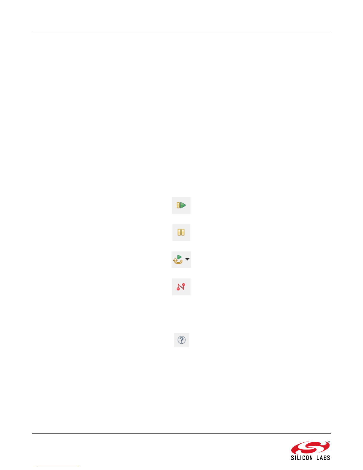
6. Click on the project in the Project Explorer and click Build, the hammer icon in the top bar. Alternatively,
go to Project
7. Click Debug to download the project to the hardware and start a debug session.
8. Press the Resume button to start the code running. The LED should blink.
Build Project.
NewSilicon Labs MCU
9. Press the Suspend button to stop the code.
10. Press the Reset the device button to reset the target MCU.
11. Press the Disconnect button to return to the development perspective.
4.2. Simplicity Studio Help
Simplicity Studio includes detailed help information and device documentation within the tool. The help contains
descriptions for each dialog window. To view the documentation for a dialog, click the question mark icon in the
window:
This will open a pane specific to the dialog with additional details.
The documentation within the tool can also be viewed by going to Help
Help Contents or HelpSearch.
6 Rev. 0.2
Page 7

C8051F96x/Si102x
4.3. Legacy 8-bit IDE
Note: Using the Simplicity Studio tools with the C8051F960 Development Kit is recommended. See section 4. "Software
Setup‚" on page 5 for more information.
Download the 8-bit software from the website (www.silabs.com/8bit-software) or use the provided installer on the
CD-ROM to install the software tools for the C8051F96x devices. After installation, examples can be found in
...\Examples\C8051F96x or ...\Examples\Si102x_3x in the installation directory. At a minimum, the C8051F960
DK requires:
Silicon Labs IDE—Software enabling initial evaluation, development, and debugging.
Configuration Wizard 2—Initialization code generation software for the C8051F96x devices.
Keil C51 Tools—Keil 8051 Compiler/Assembler/Linker toolchain.
CP210x Drivers—Virtual COM Port (VCP) drivers for th e CP210x COM interface. More information on this
installation process can be found in Section Figure 3.
Other software available includes:
Keil µVision Driver—Driver for the Keil µVision IDE that enables development and debugging on
C8051Fxxx MCUs.
Flash Programming Utilities and MCU Production Programmer—Programming utilities for the
production line. More information on the available programming options can be found on the website:
http://www.silabs.com/products/mcu/Pages/ProgrammingOptions.aspx.
ToolStick Development Tools—Software and examples for the ToolStick development platform. More
information on this platform can be found at www.silabs.com/toolstick.
Also available on the 8-bit software webpage is the Battery Life Estimator, which gives designers a quick and easy
way to understand the discharge characteristics of different system configurations to help optimize low-power
applications.
The development kit includes the latest version of the C51 Keil 8051 toolset. This toolset is initially limited to a code
size of 2 kB and programs start at code address 0x0800. After registration, the code size limit is removed entirely
and programs will start at code address 0x0000.
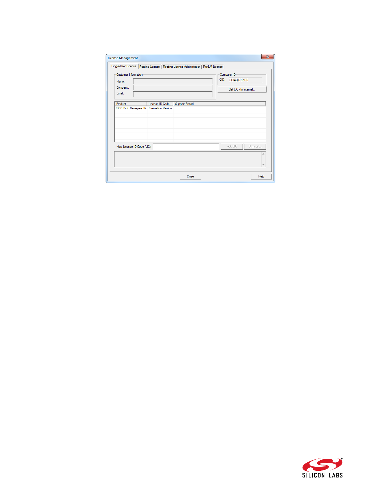
To register the Keil toolset:
1. Find the Product Serial Number printed on the CD-ROM. If you no longer have this serial number,
register on the Silicon Labs website (www.silabs.com/8bit-software) to obtain the serial number.
2. Open the Keil µVision4 IDE from the installation directory with administrative privileges.
3. Select File
License Management to open the License Management window.
Rev. 0.2 7
Page 8
C8051F96x/Si102x
Figure 5. Keil µVision4 IDE License Management Window
4. Click on the Get LIC via Internet... button to open the Obtaining a License IDE Code (LIC) window.
5. Press OK to open a browser window to the Keil website. If the window doesn’t open, navigate to
www.keil.com/license/install.htm.
6. Enter the Silicon Labs Product Serial Number printed on the CD-ROM, along with any additional required
information.
7. Once the form is complete, click the Submit button. An email will be sent to the provided email address
with the license activation code.
8. Copy the License ID Code (LIC) from the email.
9. Paste the LIC into the New License ID Code (LIC) text box at the bottom of the License Management
window in µVision4.
10. Press the Add LIC button. The window should now list the PK51 Prof. Developers Kit for Silabs as a
licensed product.
11. Click the Close button.
4.4. CP210x USB to UART VCP Driver Installation
The MCU Card includes a Silicon Labs CP210x USB-to-UART Bridge Controller. Device drivers for the CP210x
need to be installed before the PC software can communicate with the MCU through the UART interface. Use the
drivers included CD-ROM or download the latest drivers from the website (www.silabs.com/interface-software).
1. If using the CD-ROM, the CP210x Drivers option will launch the appropriate driver installer . If downloading
the driver package from the website, unzip the files to a location and run the appropriate installer for the
system (x86 or x64).
2. Accept the license agreement and follow the steps to install the driver on the system. The installer will let
you know when your system is up to date. The driver files included in this installation have been certified by
Microsoft.
3. To complete the installation process, connect the included USB cable between the host computer and the
COM PORT USB connector (J5) on the MCU Card. Windows will automatically finish the driver installation.
Information windows will pop up from the taskbar to show the installation progress.
4. If needed, the driver files can be uninstalled by selecting Windows Driver Package—Silicon
Laboratories... option in the Programs and Features window.
8 Rev. 0.2
Page 9
C8051F96x/Si102x
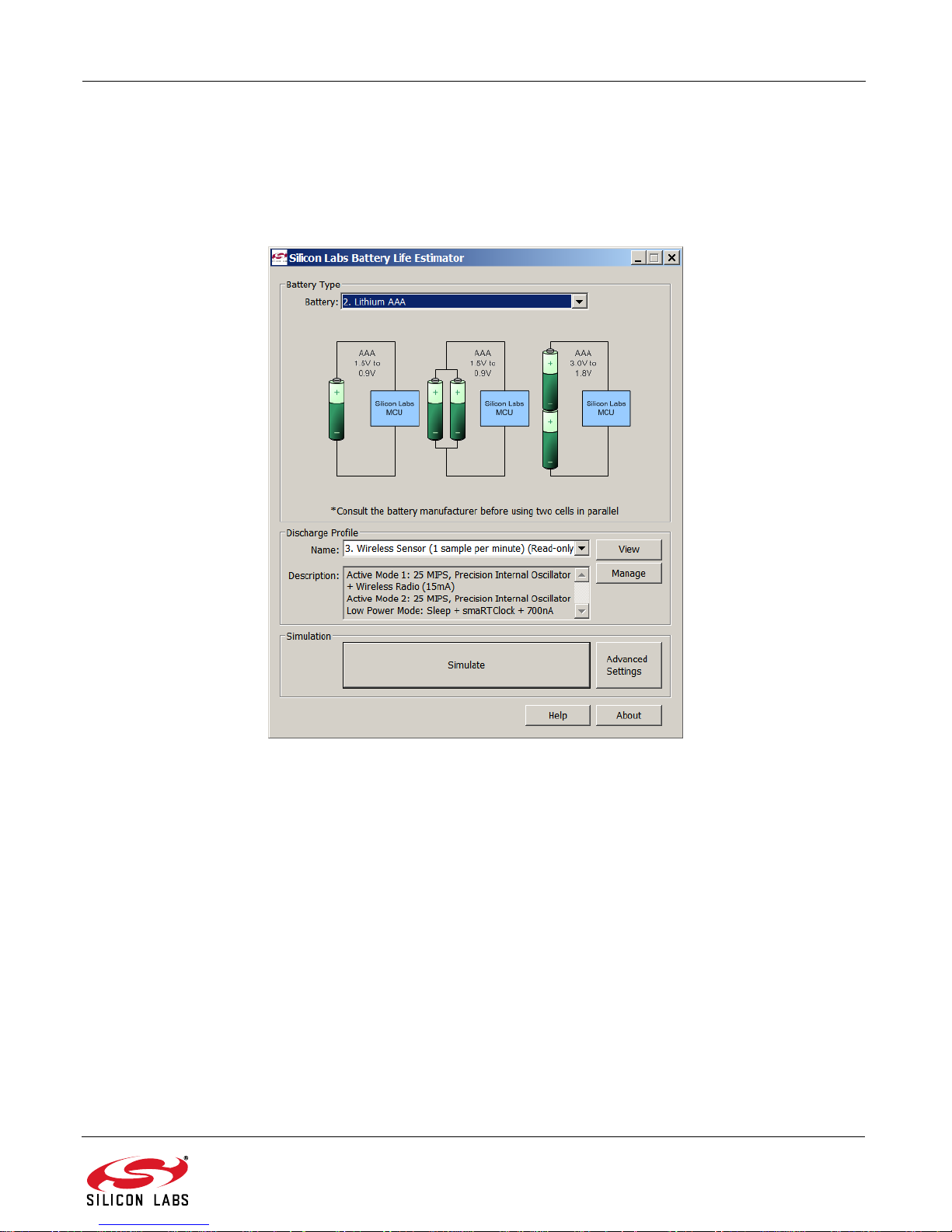
4.5. Silicon Labs Battery Life Estimator
The Battery Life Estimator is a system design tool for battery operated devices. It allows the user to select the type
of battery they are using in the system and enter the supply current profile of their application. Using this
information, it performs a simulation and provides an estimated system operating time. The Battery Life Estimator
is shown in Figure 6.
From Figure 6, the two inputs to the Battery Life Estimator are battery type and discharge profile. The utility
includes battery profiles for common battery types such as AAA, AA, A76 Button Cell, and CR2032 coin cell. The
discharge profile is application-specific and describes the supply current requirements of the system under various
supply voltages and battery configura tions. The discharge profile is independent of the selected power source.
Several read-only discharge profiles for common applications are included in the pulldown menu. The user may
also create a new profile for their own applications.
To create a new profile:
1. Select the profile that most closely matches the target application or choose the "Custom Profile".
2. Click Manage.
3. Click Duplicate.
4. Click Edit.
Profiles may be edited with the easy-to-use GUI (shown in Figure 7).
Figure 6. Battery Life Estimator Utility
Rev. 0.2 9
Page 10
C8051F96x/Si102x
Figure 7. Battery Life Estimator Discharge Profile Editor
The Discharge Profile Editor allows the user to modify the profile name and description. The four text entry boxes
on the left hand side of the form allow the user to specify the a mount of time the system spends in each power
mode. On the right hand side, the user may specify the supply current of the system in each power mode.
Since supply current is typically dependent on supply voltage, the discharge profile ed itor provides two columns for
supply current. The V2 and V1 voltages at the top of the two column s specify the voltages at which the current
measurements were taken. The Battery Life Estimator creates a linear approximation based on the input data and
is able to feed the simulation engine with an approximate supply current demand for every input voltage.
The minimum system operating voltage input field allows the system operating time to stop increasing when the
simulated battery voltage drops below a certain threshold. This is primarily to allow operating time estimates for
systems that cannot operate down to 1. 8 V, which is the voltage of two fully drained single-cell batteries plac ed in
series.
10 Rev. 0.2
Page 11
C8051F96x/Si102x
The wakeup frequency box calculates the period of a single iteration through the four power modes and displays
the system wake up frequency. This is typically the "sample rate" in low power analog sensors.
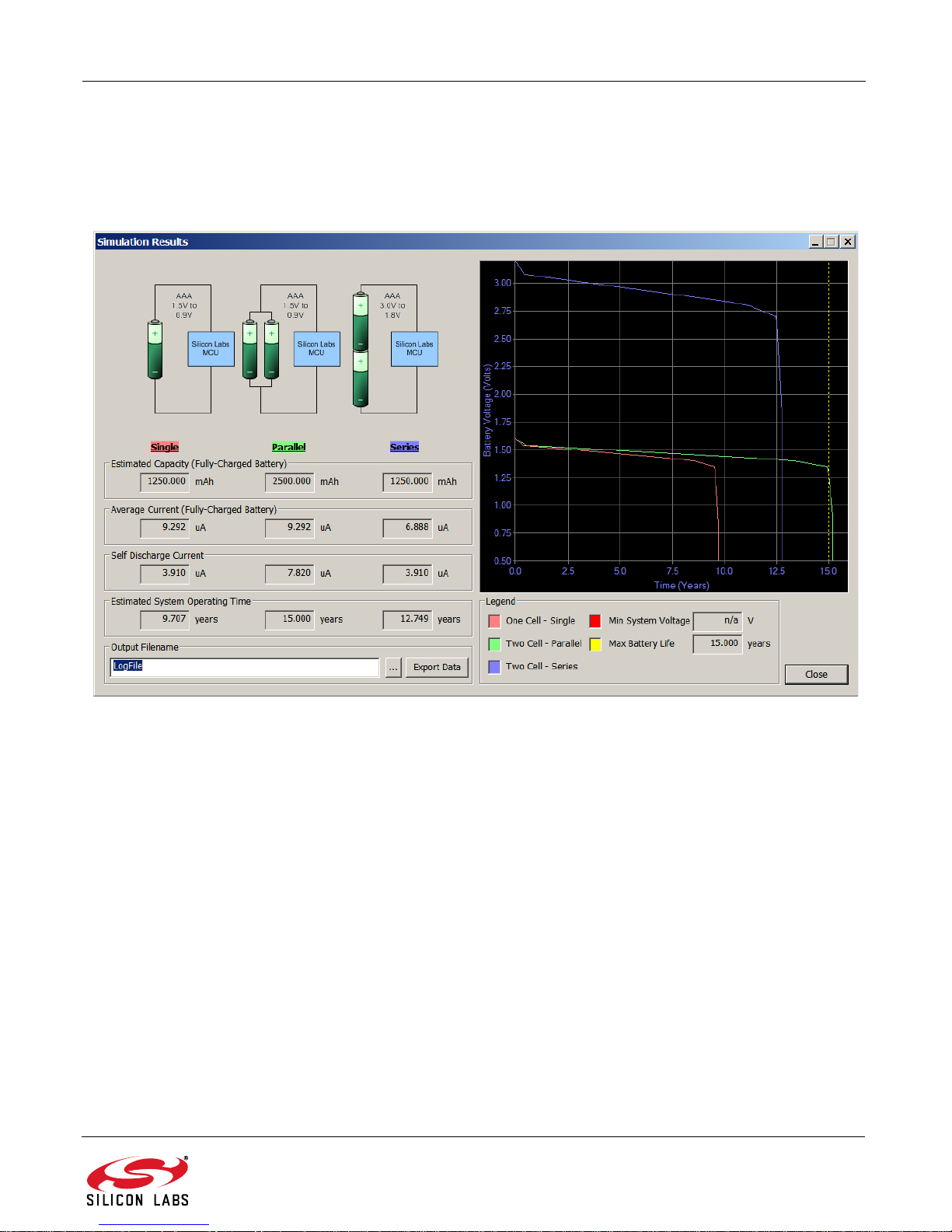
Once the battery type and discharge profile is specified, the user can click the "Simulate" button to start a new
simulation. The simulation engine calculates the estimated battery life when using one single-cell battery, two
single-cell batteries in series, and two single-cell batteries in parallel. Figure 8 shows the simulation output window.
Figure 8. Battery Life Estimator Utility Simulation Results Form
The primary outputs of the Battery Life Estimator are an e stimate d system ope ratin g time and a sim ulated gr aph of
battery voltage vs. time. Additional outputs include estimated battery capacity, average current, self-discharge
current, and the ability to export graph data to a comma delimited text file for plotting in an external graphing
application.
Rev. 0.2 11
Page 12
C8051F96x/Si102x
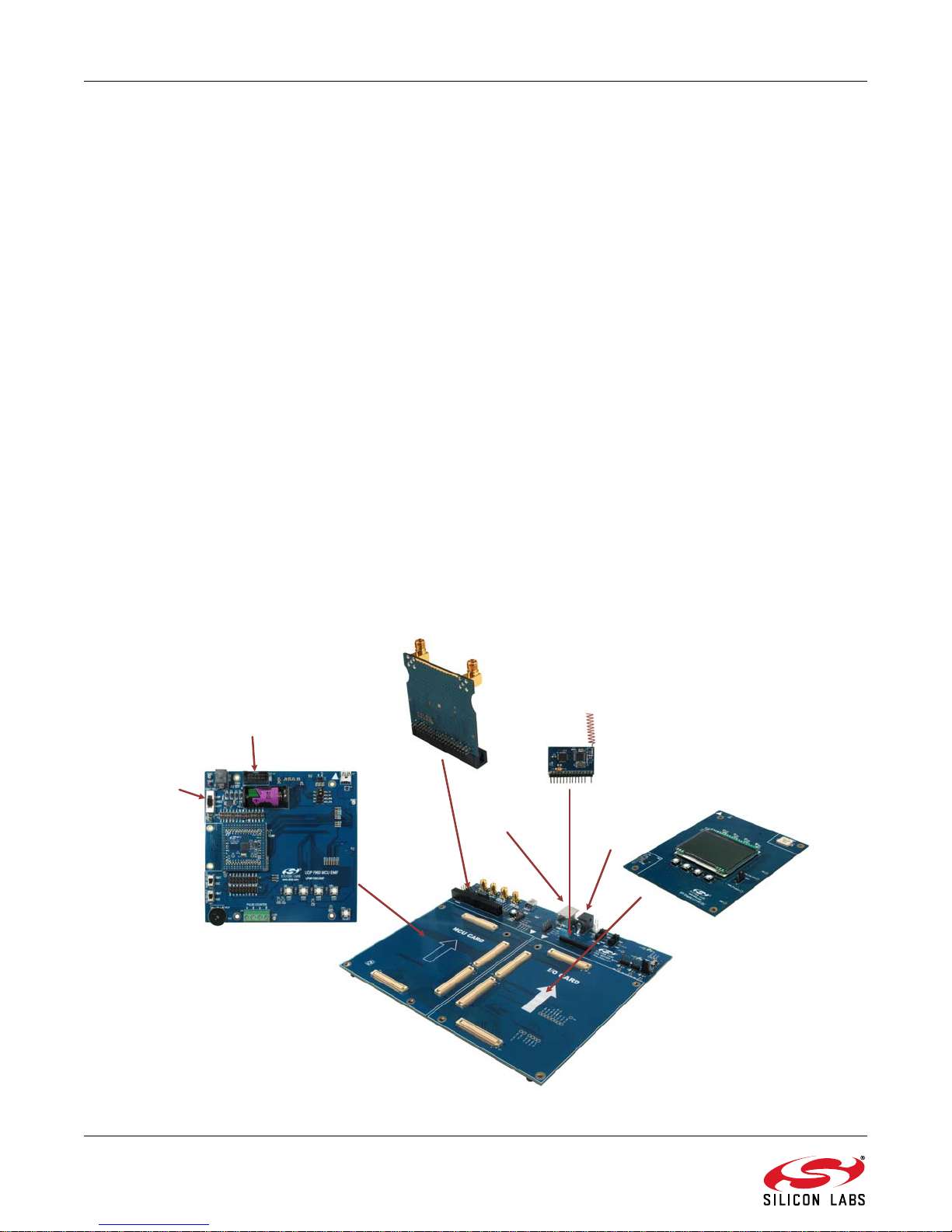
5. UDP C8051F960/Si1020 MCU Card with EMIF Overview
The C8051F96x MCU card enables application development on the C8051F960 MCU. The card connects to the
MCU Card expansion slot on the UDP motherboard and provides complete access to the MCU resources. Each
expansion board has a unique ID that can be read out of an EEPROM or MCU on the board, which enables
software tools to recognize the connected hardw are and automatically select the appropriate firmware image. The
target MCU card can also be detached from the UDP and used alone as a development or demonstration tool.
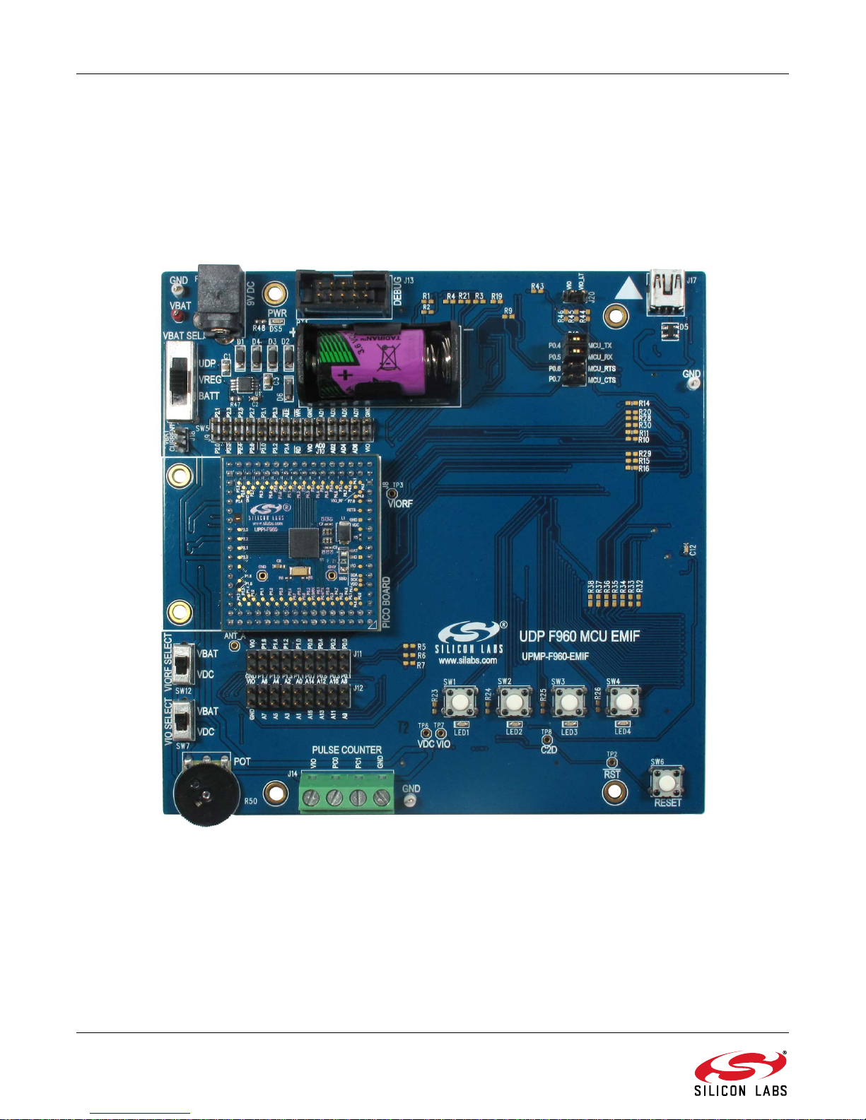
Figure 9 shows the C8051F96x MCU card.
Figure 10 highlights some of the features of the UDP C8051F960/Si1020 MCU Card with EMIF.
12 Rev. 0.2
Figure 9. C8051F96x UDP MCU Card
Page 13
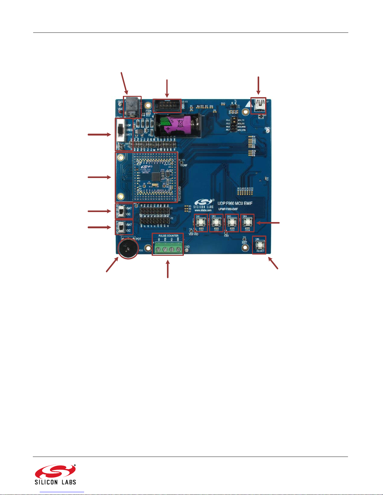
C8051F96x/Si102x
Debug Connector
9 V Wall Adapter
Connector
VIO Switch
VIORF Switch
VBAT Switch
UPPI Pico Board
Connector
Potentiometer
Pulse Counter
Terminals
Reset Push-Button
Push-Button Switches
and LEDs
Mini-B USB
Connector
5.1. UPPI Pico Board Connector (J5, J6, J7, J8)
The UPPI Pico Board connector accommodates a variety of C8051F96x and Si102x/3x UPPI Pico Boards. The
C8051F960 MCU and Si1020 Wireless MCU UPPI Pico Boards share a common form factor. This enables the
MCU card to support a wide variety of wired and wireless applications.
The supported UPPI Pico Boards include:
The Si1020/30 UPPI Pico Boards include an EZRadioPRO
include an RF transceiver; instead, these boards support most Silicon Labs 40-pin radio test cards when used with
the Unified Development Platform Motherboard.
Figure 10. UDP C8051F960/Si1020 MCU Card with EMIF
UPPI-F960
UPPI-Si1020GMxxxTR
®
transceiver. The C8051F960 UPPI Pico Boards do not
Rev. 0.2 13
Page 14

C8051F96x/Si102x
5.2. Push-Button Switches and LEDs (SW1–SW4, LED1–LED4)
The UDP C8051F960/Si1020 MCU Card with EMIF has four push-button switches. The four switches connect to
P3.0 through P3.3. The switches are normally open and pull the pin voltage to ground when pressed.
Port pins P3.0 through P3.3 also connect to four LEDs: LED1 through LED4. The LEDs connect to VIO through a
current limiting resistor.
This multiplexing arrangement reduces the number of port pins used from eight to four. Firmware may easily use
either the LED or the switch for each port pin. When using both the LED and the switch on the same port pin,
firmware must momentarily toggle off the LED by writing a 1 to the pin’s port latch to read the push-button switch
status.
5.3. VBAT Selection Switch (SW5)
The UDP C8051F960/Si1020 MCU Card with EMIF has many power options. The VBAT selector switch (SW5)
selects the power source for the main C8051F960/Si1020 VBAT supply pin.
The center VREG position selects the output of the on-board 3.3 V re gulator (U1). This is the pr imary supp ly option
for development. The on-board regulator has multiple 5 V and 9 V power sources connected via Schottky diodes to
the regulator input. The highest voltage power source will supply power to the regulator.
The power sources for the on-board regulator (U1) are as follows:
9 V DC Wall Adapter power receptacle (P1).
Mini-B USB receptacle (J17).
10-pin Debug connector (J13).
UDP motherboard +5 V (when connected).
The BATT position selects the ultra long life 3.6 V lithium thionyl chloride battery (BT1). This batter y is a typical
power source for metering applications. The o n-boa rd r egu lator should be used primaril y for de velopment becau se
the battery has a limited peak current capacity.
The UDP position on the VBA T selector selects the UDP motherbo ard progra mmable supply (PWR_VDD_OUT) as
the power source for the UPPI Pic o Board. Use this position when using the programmable power supply under
software control.
The UDP motherboard can also provide power to the on-board regulator. The VREG position will always work with
the motherboard, while the UDP switch position requires some motherboard configuration. The UDP motherboard
User’s Guide contains additional information.
The VBAT voltage and ground are available on test points in the top-left corner of the MCU card. Use these test
points to power the board from an external lab power supply. When using a lab supply, the VBAT selector switch
should be in the BATT position with the battery removed.
5.4. Debug Header (J13)
The standard 10-pin debug header supports the Silicon Labs USB Debug Adapter. This connector provides a C2
debug connection to C8051F960/Si1020 on the UPPI Pico Board. The USB Debug Adapter supports two types of
debug connections: C2 and JTAG. When using this MCU card with the Silicon Labs IDE, select C2 in the
connection options dialog before connecting.
The USB Debug Adapter also provides a 5 V power source that can power the regulator. When powering the MCU
from the debug connector, the VBAT switch must be in the VREG position. Additionally, select the Power Target
after Disconnect check box in the Silicon Labs IDE connections options dialog to ensure the MCU always has
power.
5.5. Reset Button (SW6)
The reset push-button switch is in the lower-right corner. Pushing this button will always reset the MCU. Note that
pushing this button while the IDE is connected to the MCU will result in the IDE disconnecting from the target.
14 Rev. 0.2
Page 15

C8051F96x/Si102x
5.6. Pin Power Supply Select Switches
The C8051F960/Si1020 MCU has two VIO pins: VIO and VIORF. These VIO pins set the logic level and drive
voltage for the MCU port pins. The VIORF pin sets the level for the port pins n ormally supporting r adio functiona lity:
P1.5 through P2.3. The Si1020 P2.0-2.3 pins are connected internally to the EZRadioPRO. The VIO pin sets the
level for all other port pins.
5.6.1. VIORF Select Switch (SW12)
When using the dc-dc buck con verter to pow er the radio, set the VIOR F selector switc h to the VDC po sition. This
connects the output of the buck converter to the VIORF pin. When using the Si1020, this switch also selects the
power source for the radio. In this position, firmwar e controls the voltage on the VDC pin. The C8051F960/Si1020
buck converter also has a bypass switch that can power the radio from the full supply voltage. The dc-dc buck
converter and bypass switch are off by default after an MCU reset, so the VDC pin voltage is floating until firmware
turns on the bypass switch or configures the dc-dc converter.
When the VIORF selector switch is set to the VBAT position, the VIORF pin connects via hardware to the VBAT
pin. In this position, the dc-dc buck converter cannot power the radio.
The VBAT position powers the VIORF pin without any firmware. This position is more convenient for simple code
examples. Use this position for the code ex am p les pr ovided unless otherwise indicated.
5.6.2. VIO Select Switch (SW7)
The VIO selector switch provides the same functionality as the VIORF switch for the main VIO pin. Normally this
switch should be in the VBAT position, which will set the drive and input levels of the pins to VBAT.
Setting the switch to the VDC position connects the VIO pin to the output of the buck converter. In this position, the
battery powers the MCU, and all of the I/O port s oper ate at a lo wer vo lt age set by the buck conve rter. This option is
best if most of the I/O pins connect to a low voltage radio or other low-volt age periphe rals. Most applications should
use the VBAT position.
The C2 connection requires a VIO power source and VDC is not powered by default, so the VBAT position must be
used for initial development.
5.7. UART VCP Connection Options
The MCU card features a USB virtual COM port (VCP) UART connection via the mini-B USB connector (J17). The
VCP connection uses the CP2102 USB-to-UART bridge chip.
The UART pins on the target MCU either connect to the CP2102 USB-to-UART bridge chip or to the UDP
motherboard. The MCU card has level translators with enables that normally route the UART connections to the
on-board USB-to-UART bridge chip. However, the UDP motherboard can drive the enable pins to route the UART
connections to the UDP motherboard instead of the on-board USB-to-UART bridge chip. There are two enable
signals: one with a default pull-down (UART_VCP_EN) and one with a default pull-up (UART_SYS_EN).
When using the UART with either the on-board USB-to-UART bridge or the UDP motherboard, install shorting
blocks on header P12 to connect P0.4 to MCU_TX and P0.5 to MCU_RX.
If desired, install shorting blocks for hardware handshaking on P0.6 and P0.7 on the P12 header. Hardware
handshaking is not required for most applications. Firmware must implement hardware handshaking on the target
MCU using P0.6 and P0.7. These pins also connect to the 40-pin radio card I2C signals by default. If necessary,
disconnect these signals by cutting the traces on R9 and R10.
The MCU card includes provisions to facilitate ultra-low power measurements. The UART pins of the target MCU
are completely disconnected from the USB-to-UART bridge by removing all the shorting blocks on P12. The VIO
supply powers the level translator. To remove the level-shifter current from the ultra-low power measurement, cut
the trace on the bottom of the board between the two pins of header J20. This will completely disconnect the level
translators from VIO. After cutting this trace, a shorting block is required on J20 to use the USB-to-UART bridge or
UDP UART connection.
Rev. 0.2 15
Page 16

C8051F96x/Si102x
5.8. Potentiometer (R50)
The potentiometer is available on P1.4. To facilitate a low-power potentiometer, P2.7 connects to bottom of the
potentiometer as a potentiometer enable (POT_EN). Drive P2.7 low to enable the potentiometer. Alternatively,
install a 0 resistor for R51 to continuously enable the potentiometer.
5.9. Pulse Counter Terminals (J14)
The MCU card includes a 4-position screw terminal connection. These field-wiring terminals will accept large wire
for a commercial water or gas meter. The PC0 and PC1 signals connect to P1.0 and P1.1 on the target MCU.
These are dedicated pins for th e C8051F960/Si1020 low-power pulse counter. The VIO and ground connections
are also available for Form C meters. Refer to the C8051F960 dat a sheet for addition al infor mation abou t the pulse
counter.
5.10. Port Pin Headers (J9-J12)
All of the MCU port pins are available on the 0.100 inch headers on either side of the UPPI Pico Board.
Pins P1.2 and P1.3 are normally used for the RTC and are not connected by default to the P1.2 an d P1 .3 he ad ers.
To use P1.2 and P1.3 for other purposes, remove the RTC crystal on the UPPI Pico Board and populate the two
small adjacent resistors with 0 resistors.
When using the Si1020 UPPI Pico Board, the SPI1 pins are connected internally and do not connect to the header
pins.
16 Rev. 0.2
Page 17

C8051F96x/Si102x
5.11. C8051F96x Board Default and Optional Connections
The C8051F96x MCU card has many default and optional connections for use with different radios and the UDP
motherboard. The default connections have shorting jumpers consisting of a 603 resistor footprint with a trace
between the pads. To disconnect a default connection, cut the trace between the pads. To reconnect, install a 0
603 resistor or connect the two pads with solder. The optional connections are non-populated (no-pop) resistor
footprints. To connect, install a 0 603 resistor or connect the two pads with solder.
When using the Si1020 UPPI Pico Board, some of the MCU port pins connect to EZRadioP RO port pins by default.
Note that plugging the UPPI Pico Board into the MCU card will connect some pins together.
Table 1 shows a summary of the default and optional connections for each pin.
Table 1. MCU Pin Functions
MCU Pin
P0.0 SPI_LCD_SCK EBID_SCK
P0.1
P0.2
P0.3
P0.4/TX TX
P0.5/RX RX
P0.6 CTS EZR_I2C_SDA
P0.7 RTS EZR_I2C_SCL GPIO2
P1.0 PC0
P1.1 PC1
P1.2 XTAL3
P1.3 XTAL4
P1.4 POT EZR_ARSSI
P1.5 GPIO_1
P1.6
P1.7 EZRP_SDN
P2.0/SCK1 EZRP_SCK
P2.1/MISO1 EZRP_MISO
P2.2/MOSI1 EZRP_MOSI
P2.3/NSS1 EZRP_NSS
P2.4 PIEZO
P2.5 GPIO_0 EZRP_TX_DATA_IN/
P2.6 SPI_LCD_A0
P2.7 POT_EN
P3.0 SW1/LED1
P3.1 SW2/LED2
MCU Card Function UDP Motherboard Signal
Default Optional Default Optional
SPI_LCD_MISO EBID_MISO
SPI_LCD_MOSI EBID_MOSI
VREF SPI_LCD_NSS
EZRP_RX_DOUT/
EZRP_GPI0_1
EZRP_NIRQ
EZRP_GPIO_0
EZR_FFIT
Rev. 0.2 17
Page 18

C8051F96x/Si102x
Table 1. MCU Pin Functions (Continued)
MCU Pin
P3.2 SW3/LED3
P3.3 SW4/LED4
P3.4 RF_EBIF_NSS
P4.6 ANT_A EZR_CLKIN/
P4.7 GPIO2 EZRP_RX_CLKOUT/
5.11.1. P0.0 through P0.3
Pins P0.0 through P0.3 connect to the UDP SPI_LCD signals (SPI_LCD_SCK, SPI_LCD_MISO, SPI_LCD_MOSI,
SPI_LCD_NSS) by default. These signals support th e optional Graphical LCD display I/O card when used with the
UDB motherboard. To disconnect these default connections, cut the traces on R1 through R4. Optionally, these
signals can also connect to the EBID SPI on the 40-pin radio card. R8 provides an option to use P0.0 as a voltage
reference.
5.11.2. P0.6
Pin P0.6 connects to EZRP_I2C_SDA b y default. This si gnal supports I2C radios and EZRadio transceivers using
the 40-pin radio connector on the UDP motherboard.
5.11.3. P0.7
Pin P0.7 connects to EZRP_I2C_SCL by default. This signal supports I2C radios using the 40-pin radio connector
on the UDP motherboard. The MCU card provides optional conne ctions to co nnect P0.7 to EZ RP_RX_CL KOUT or
use P0.7 as the IREF current reference pin.
MCU Card Function UDP Motherboard Signal
Default Optional Default Optional
EZRP2_GPIO3
EZRP_GPIO2
5.11.4. P1.4
Pin P1.4 normally connects to the potentiometer. Optionally, P1.4 can connect to EZR_ARSSI. This signal supports
an analog RSSI measurement using an EZRadio 40-pin test card.
5.11.5. P1.5
Pin P1.5 connects to GPIO_1 via R15 and R29 by default. To disconnect this signal, cut the trace on R15. This
signal supports the clear-to-send (CTS) signal for EZRadioPRO.
5.11.6. P1.6
Pin P1.6 normally connects to nIRQ us ing R17. Cut the tr ace on R17 to disconnect these signals. Note that P1.7
also connects to nIRQ on the UPPI Pico Board, so a trace on the UPPI Pico Board must also be cut.
5.11.7. P1.7
Pin P1.7 connects to SDN via R18. To disconnect these signals, cut the trace on R18. P1.7 also connects to SDN
on the UPPI Pico Board, so it is necessary to also cut a trace on the UPPI Pico Board.
5.11.8. P2.4
P2.4 normally connects to the PIEZO signal. This signal drives a piezo transducer on the graphical LCD I/O card.
5.11.9. P2.5
Pin P2.5 connects to the GPIO_0 via R20 and R28 b y default. Cut the trace on R20 to disconnect these signals.
This signal supports direct mode communication with the Si1020 EZRadio.
5.11.10. P3.6
P3.6 normally connects to SPI_LCD_A0. This signal supports the Graphical LCD display I/O card.
18 Rev. 0.2
Page 19

C8051F96x/Si102x
5.11.11. EZRadio GPIO Signals
When using a Si1020 UPPI Pico Board, the four EZRadioPRO GPIO signals connect to the SMA connectors on
the motherboard.
GPIO_0 connects to EZRP_TX_DATA_IN via R20. This signal supports direct mode TX input data from an external
source using the SMA connector.
GPIO_1 connects to EZRP_RX_DOUT via R21. This signal supports direct mode RX data out of the SMA
connector. Normally, the RX data out is used with the RX clock out.
GPIO_2 connects to EZRP_RX_CLK_OUT via R22. This signal supports direct mode RX data out of the SMA
connector.
ANT_A connects to EZR_CLK_IN using R23. This provides a connection to the forth SM A co nnector. Cut the trace
on R23 when using an external 10 MHz clock with EZRadio.
5.11.12. EMIF Connections
Some of the EMIF lines also connect to the 40-pin rad io card connector. EMIF_A15/- connects to GPIO_2, and
EMIF_A14/- connects to GPIO_3. Disconnect these signals when using the EMIF in 16-bit address nonmultiplexed mode.
Table 2 describes the C8051F96x MCU card’s EMIF connections.
Table 2. MCU EMIF Connections
EMIF Configurations
MCU Pin
Non-Multiplexed Multiplexed
MCU Card Signal
Name
UDP Motherboard
Signal Name
16-bit 8-bit 16-bit 8-bit
P3.5 ALE ALE EMIF_ALE EMIF_ALE
P3.6 /RD /RD /RD /RD EMIF_RD EMIF_OEB
P3.7 /WR /WR /WR /WR EMIF_WR EMIF_WRB
P4.0 A8
P4.1 A9
P4.2 A10
P4.3 A11
P4.4 A12
P4.5 A13
P4.6 A14
P4.7 A15
P5.0 A0 A0 A8
P5.1 A1 A1 A9
P5.2 A2 A2 A10
P5.3 A3 A3 A11
P5.4 A4 A4 A12
P5.5 A5 A5 A13
P5.6 A6 A6 A14
P5.7 A7 A7 A15
P6.0 D0 D0 AD0 AD0 EMIF_D0/AD0 EMIF_A0
P6.1 D1 D1 AD1 AD1 EMIF_D1/AD1 EMIF_A1
P6.2 D2 D2 AD2 AD2 EMIF_D2/AD1 EMIF_A2
EMIF_A8/- EMIF_A16
EMIF_A9/- EMIF_A17
EMIF_A10/- EMIF_A18
EMIF_A11/- EMIF_A19
EMIF_A12/- EMIF_A20
EMIF_A13/- EMIF_A21
EMIF_A14/- EMIF_A22
EMIF_A15/- EMIF_A23
EMIF_A0/A8/- EMIF_A8
EMIF_A1/A9/- EMIF_A9
EMIF_A2/A10/- EMIF_A10
EMIF_A3/A11/- EMIF_A11
EMIF_A4/A12/- EMIF_A12
EMIF_A5/A13/- EMIF_A13
EMIF_A6/A14/- EMIF_A14
EMIF_A7/A15/- EMIF_A15
Rev. 0.2 19
Page 20

C8051F96x/Si102x
Table 2. MCU EMIF Connections (Continued)
EMIF Configurations
MCU Pin
Non-Multiplexed Multiplexed
MCU Card Signal
Name
UDP Motherboard
Signal Name
16-bit 8-bit 16-bit 8-bit
P6.3 D3 D3 AD3 AD3 EMIF_D3/AD3 EMIF_A3
P6.4 D4 D4 AD4 AD4 EMIF_D4/AD4 EMIF_A4
P6.5 D5 D5 AD5 AD5 EMIF_D5/AD5 EMIF_A5
P6.6 D6 D6 AD6 AD6 EMIF_D6/AD6 EMIF_A6
P6.7 D7 D7 AD7 AD7 EMIF_D7/AD7 EMIF_A7
20 Rev. 0.2
Page 21

C8051F96x/Si102x
6. Using the C8051F96x with the UDP Motherboard
6.1. VBAT Selector Switch
When used with the UDP motherboard, the motherboard can power the C8051F96x MCU card. With the VBAT
selector switch in the VREG position, the motherboard powers the regulator on the card. With the VBAT selector
switch in the UDP position, the UDP motherboard powers VBAT directly. This position supports software control of
the variable voltage power supply and current measurements.
The S1 switch on the UDP motherboard select s between th e fixed o r programmable volt age. The varia ble supply is
controlled by the C8051F384 board control MCU through the U1 digital potentiometer. Use the fixed supply when
the variable supply is not under software control.
6.2. MCU Card Header Connections
The C8051F96x MCU card has four connectors with 100 pins each. These 400 pins are directly tied to th e UDP
motherboard and I/O cards. These signals are named and designed to support a wide variety of features and
applications, and the UDP C8051F960/Si1020 MCU Card with EMIF card implements a subset of these
connections.
The MCU cards and I/O cards are designed so that a maximum number of functions are shared between each
card. This allows a particular type of I/O card to be shared amongst all MCU cards that connect to the same
signals.
The MCU card slot includes the following components:
J1 MCU card connector H1
J2 MCU card connector H2
J3 MCU card connector H3
J4 MCU card connector H4
The C8051F96x MCU card implements the signals described in Table 4, Table 5, Table 6, and Table 7 in the
Appendix.
Rev. 0.2 21
Page 22

C8051F96x/Si102x
6.3. Shorting Blocks: Factory Defaults
The UDP C8051F960/Si1020 MCU Card with EMIF comes from the factory with pre-installed shorting blocks on
several headers. Figure 11 shows the positions of the factory default shorting blocks.
Figure 11. Shorting Blocks: Factory Defaults
Shorting blocks are installed on P2 to connect P0.4 to MCU_TX and P0.5 to MCU_RX.
22 Rev. 0.2
Page 23

7. Schematics
C8051F96x/Si102x
Figure 12. C8051F96x UDP MCU Card Schematic (1 of 6)
Rev. 0.2 23
Page 24

C8051F96x/Si102x
24 Rev. 0.2
Figure 13. C8051F96x UDP MCU Card Schematic (2 of 6)
Page 25

C8051F96x/Si102x
Figure 14. C8051F96x UDP MCU Card Schematic (3 of 6)
Rev. 0.2 25
Page 26
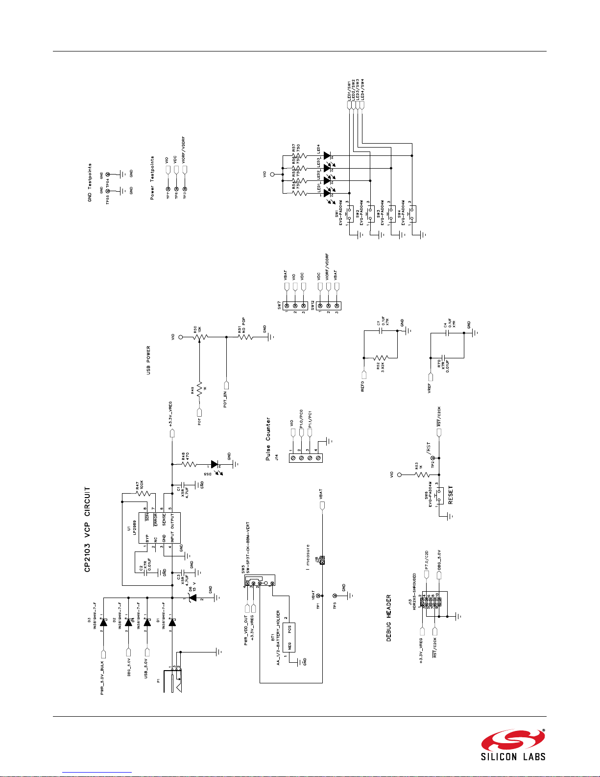
C8051F96x/Si102x
26 Rev. 0.2
Figure 15. C8051F96x UDP MCU Card Schematic (4 of 6)
Page 27

C8051F96x/Si102x
Figure 16. C8051F96x UDP MCU Card Schematic (5 of 6)
Rev. 0.2 27
Page 28

C8051F96x/Si102x
28 Rev. 0.2
Figure 17. C8051F96x UDP MCU Card Schematic (6 of 6)
Page 29

C8051F96x/Si102x
8. Bill of Materials
Table 3. UDP C8051F960/Si1020 MCU Card with EMIF Bill of Materials
Reference Part Number Source Description
U2 24AA64T-I/MNY Microchip Technology 64KBIT I2C SERIAL FLASH, 400kHZ, 8-
TDFN
U4-5 SN74AVC4T245PWR Texas Instruments Quad Dual-Supply Level Shifter, TSSOP
BT1 12BH1/2AA-2P-GR Eagle Plastic Devices HOLDER BATTERY, 1/2 CELL AA, PCB
MNT OR EQ, RoHS
C2, C12,
R70
C4-8, C10-
11, C13
C14 GRM188R71A105KA61D Murata Electronics
C15 GRM188R71A105KA61D Murata Electronics
C1, C3, C9 EMK212BJ475KG-T Taiyo Yuden CAP, 4.7UF, X5R, CERAMIC, 0805, 16V,
P1 RAPC722X Switchcraft Inc CONN, POWERJACK MINI.08" RA PC
J1-4 FX8-100P-SV1(91) Hirose Electric Co Ltd CONN, HDR, 100POS, .6MM, GOLD, SMD,
U63 CP2102 Silicon Labs SINGLE-CHIP USB TO UART BRIDGE,
D1-4 1N5819HW-7-F Diodes Inc DIODE SCHOTTKY, 40V, 1A, SOD123,
D6 MMSZ5245B-7-F Diodes Inc DIODE, ZENER, 15V, 500MW, SMT,
D5 SP0503BAHTG Littelfuse Inc TVS AVAL DIODE ARRAY, 3 CH, SOT143,
J7-8 25631401RP2 Norcomp Inc. 14POS, 2MM VERT SGL ROW
J18, J20 PBC02SAAN Sullins Connector
P12 PBC04DAAN Sullins Connector
J10 PBC05DAAN Sullins Connector
J9, J11-12 PBC09DAAN Sullins Connector
J5-6 A3C-32DA-2DSC(71) Hirose Electric Co Ltd HEADER RECEPTACLE, 32 POS, 2MM,
J13 N2510-6002-RB 3M HEADER, SHROUDED, 2X5, OR EQ,
L1 NLV25T-R68J-PF TDK INDUCTOR, POWER, 0.68UH, 1008 SMD,
06035C103KAT2A AVX Corporation CAP, 0.01UF (10000PF), X7R, CERAMIC,
0603, 50V, ±10%, OR EQ, RoHS
C0603C104J3RACTU Kemet CAP, 0.1UF, X7R, CERAMIC, 0603, 25V,
±5%, OR EQ, RoHS
CAP CERAMIC, 1.0UF, X5R, 0603, 10V,
North America
CAP CERAMIC, 1.0UF, X5R, 0603, 10V,
North America
STAKE HEADER, 1X2, 0.1"CTR, GOLD,
Solutions
STAKE HEADER, 2X4, 0.1"CTR, OR EQ,
Solutions
STAKE HEADER, 2X5, 0.1"CTR, GOLD,
Solutions
STAKE HEADER, 2X9, 0.1' CTR GOLD,
Solutions
±10%, RoHS
±10%, RoHS, NOPOP
±10%, OR EQ, RoHS
MNT, RoHS
RoHS
QFN28, RoHS
RoHS
SOD123, RoHS
RoHS
RECEPTACLE
OR EQ, RoHS, NOPOP
RoHS
OR EQ, RoHS
OR EQ, RoHS
DUAL ROW
RoHS
RoHS, NOPOP
Rev. 0.2 29
Page 30

C8051F96x/Si102x
Table 3. UDP C8051F960/Si1020 MCU Card with EMIF Bill of Materials (Continued)
Reference Part Number Source Description
DS5, LED1-4 SML-LX0603IW-TR Lumex
Opto/Components Inc
U1 LP2989AIMM-3.3/NOPB National
Semiconductor
R50 RV100F-30-4K1B-B10K-
B301
R47 ERJ-3GEYJ104V Panasonic - ECG RES, 100K, SMT, 0603, 1/10W, ±5%, OR
R41-42 ERJ-3EKF1002V Panasonic - ECG RES, EQ. 10.0K OHM, SMT, 0603, 1/10W,
R49, R53 ERJ-3EKF1001V Panasonic - ECG RES, 1K OHM, SMT, 0603, 1/10W, ±1%,
R52 ERJ-3EKF3921V Panasonic - ECG RES, 3.92K OHM, SMT, 0603, 1/10W, ±1%,
R40 ERJ-3EKF4751V Panasonic - ECG RES, 4.75K OHM , SMT, 0603, 1/10W,
R48 MCR03EZPJ471 Rohm Semiconductor RES, 470 OHM, SMT, 0603, 1/10W, ±5%,
R54-57 ERJ-3EKF7500V Panasonic - ECG RES, 750 OHM, SMT, 0603, 1/10W, ±1%,
R5-8, R11-
12, R14,
R16, R34-38,
R51
R1-4, R9-10,
R13, R15,
R17-33, R39,
R43-46
SW7, SW12 OS102011MS2QN1 C&K Components SWITCH, SPDT, 12VDC, OR EQ, RoHS
SW1-4, SW6 EVQ-PAD04M Panasonic - ECG SWITCH, LIGHT TOUCH, 130GF, 6MM SQ,
SW5 OS103012MU1QP1 C&K Components SWITCH SLIDE SP3T COMPACT PIN,
J14 1729144 Phoenix Contact CONN TERM BLOCK, 5.08MM CTRS PCB,
J17 54819-0519 Molex Inc CONN, USB MINI RECEPT, 5POS RT
Alpha (T aiwan) POT , 10K, THUMBWHEEL LINEAR, 0.03W,
LED, RED DIFF, 635NM, SMT0603, OR
EQ, RoHS
LDO REG, 500MA, ADJ, MSOP, RoHS
±20%, OR EQ, RoHS
EQ, RoHS
±1%, OR EQ, RoHS
OR EQ, RoHS
OR EQ, RoHS
±1%, OR EQ, RoHS
OR EQ, RoHS
OR EQ, RoHS
RES, SMT, 0603, OR EQ, RoHS, NOPOP
0603 SHORT, NOPOP
RoHS
PCB MNT, OR EQ, RoHS
4 POS, RoHS
ANG, TYPE B OR EQ, RoHS
30 Rev. 0.2
Page 31

C8051F96x/Si102x
APPENDIX—MCU CARD HEADER PIN DESCRIPTIONS
Table 4. UDP C8051F960/Si1020 MCU Card with EMIF H1 Pin Descriptions (J1)
MCU Card
Pin
1GND
2 USART_TX_A
3 USART_RX_A
4 USART_RTS_A
5 USART_CTS_A
6 USART_UCLK_A
7 CAN_TX_B
8 CAN_RX_B
9 SPI_SCK_A Graphical LCD I/O Card SPI clock
10 SPI_MISO_A Graphical LCD I/O Card SPI master-in, slave-out
11 SPI_MOSI_A Graphical LCD I/O Card SPI master-out, slave-in
12 SPI_NSS0_A Graphical LCD I/O Card SPI slave select
13 SPI_NSS1_A Graphical LCD I/O Card A0 address signal
14 SPI_NSS2_A
15 SPI_NSS3_A
16 USART_TX_B
17 USART_RX_B
18 USART_RTS_B
19 USART_CTS_B
20 USART_UCLK_B
21 EPCA_ECI_A
22 EPCA_CH0_A
23 EPCA_CH1_A
24 EPCA_CH2_A
25 EPCA_CH3_A
26 EPCA_CH4_A
27
28
29
30
31
32
33
34
35
36
Signal Name Usage
EPCA_CH5_A
LIN_TX_A
LIN_RX_A
PCA_ECI_A
PCA_CH0_A Graphical LCD I/O Card Piezo
PCA_CH1_A
PCA_ECI_B
PCA_CH0_B
PCA_CH1_B
I2SOUT_DFS_A
Rev. 0.2 31
Page 32
C8051F96x/Si102x
Table 4. UDP C8051F960/Si1020 MCU Card with EMIF H1 Pin Descriptions (J1) (Continued)
MCU Card
Pin
37
38
39
40
41
42
43
44
45
46
47
48
49
50 GND
51 UART_RX_SYS System UART receive
52 UART_RTS_SYS System UART hardware handshaking
53 UART_CTS_SYS System UART hardware handshaking
54 SPI_SCK_EZR EZRadioPRO SPI clock (P2.0)
55 SPI_MISO_EZR EZRadioPRO SPI master-in, slave-out (P2.1)
56 SPI_MOSI_EZR EZRadioPRO SPI master-out, slave-in (P2.2)
57 SPI_NSS0_EZR
58 SPI_NSS1_EZR
59 SPI_NSS2_EZR
60
61
62
63 I2SIN_DFS_A
64 I2SIN_CLK_A
65 I2SIN_DOUT_A
66 CLKOUT0
67 GPIO00 LED1/SW1
68 GPIO01 LED2/SW2
69 GPIO02 LED3/SW3
70 GPIO03 LED4/SW4
71 GPIO04 LED1/SW1
72 GPIO05 LED2/SW2
73 GPIO06 LED3/SW3
Signal Name Usage
I2SOUT_CLK_A
I2SOUT_DOUT_A
I2C_SDA_EZR EZRadioI2C data
I2C_SCL_EZR EZRadio I2C clock
TIMER_CT_A
TIMER_EX_A
TIMER_CT_B
TIMER_EX_B
UART_TX_A UART A transmit
UART_RX_A UART A receive
UART_RTS_A
UART_CTS_A
UART_TX_SYS System UART transmit
SPI_NSS3_EZR
I2C_SDA_B EZRadioPRO I2C data
I2C_SCL_B EZRadioPRO I2C clock
UART A hardware handshaking
UART A hardware handshaking
EZRadioPRO SPI slave select (P2.3)
32 Rev. 0.2
Page 33

C8051F96x/Si102x
Table 4. UDP C8051F960/Si1020 MCU Card with EMIF H1 Pin Descriptions (J1) (Continued)
MCU Card
Pin
74 GPIO07 LED4/SW4
75 GPIO08 Graphical LCD I/O Card Backlight
76 GPIO09
77 GPIO10
78 GPIO11
79 GPIO12
80 GPIO13
81
82 GPIO15
83 PORT_MATCH0
84 PORT_MATCH1
85
86
87
88 EXT_INT1
89 EXT_ADC_TRIG0
90 EXT_ADC_TRIG1
91 EXT_DAC_TRIG0
92 EXT_DAC_TRIG1
93 EXT_DMA_TRIG0
94 EXT_DMA_TRIG1
95 CAN_TX_A
96 CAN_RX_A
97 LIN_TX_B
98 LIN_RX_B
99 LPTIMER_IN_A
100 LPTIMER_OUT_A
Signal Name Usage
GPIO14
WAKEUP0
WAKEUP1
EXT_INT0
Rev. 0.2 33
Page 34

C8051F96x/Si102x
Table 5. UDP C8051F960/Si1020 MCU Card with EMIF H2 Pin Descriptions (J2)
MCU Card
Pin
1GND
2 UDPBUS_SDA_A Electronic Board ID I2C data
3 UDPBUS_SCL_A Electronic Board ID I2C clock
4 EPCA_ECI_MOTOR
5 EPCA_CH0_MOTOR
6 EPCA_CH1_MOTOR
7 EPCA_CH2_MOTOR
8 EPCA_CH3_MOTOR
9 EPCA_CH4_MOTOR
10 EPCA_CH5_MOTOR
11 HVGPIO0
12 HVGPIO1
13 HVGPIO2
14 HVGPIO3
15 HVGPIO4
16 HVGPIO5
17 HVGPIO6
18 HVGPIO7
19 EMIF_A23 EMIF A15/- (non-mux/mux)
20 EMIF_A22 EMIF A14/21 EMIF_A21 EMIF A13/-)
22 EMIF_A20 EMIF A12/23 EMIF_A19 EMIF A11/24 EMIF_A18 EMIF A10/25 EMIF_A17 EMIF A9/26 EMIF_A16
27
28
29
30
31
32
33
34
35
36
37
Signal Name Description
EMIF A8/-
EMIF_A15
EMIF_A14
EMIF_A13
EMIF_A12
EMIF_A11
EMIF_A10
EMIF_A9
EMIF_A8
EMIF_A7
EMIF_A6
EMIF_A5
EMIF A7/A15/- (non-mux/16-bit mux/8-bit mux)
EMIF A6/A14/EMIF A5/A13/-
EMIF A4A12/-
EMIF A3/A11/-
EMIF A2/A10/-
EMIF A1/A9/EMIF A0/A8/-
EMIF D7/AD7 (non-mux/mux)
EMIF D6/AD6
EMIF D5/AD5
34 Rev. 0.2
Page 35

C8051F96x/Si102x
Table 5. UDP C8051F960/Si1020 MCU Card with EMIF H2 Pin Descriptions (J2)
MCU Card
Pin
38
39
40
41
42
43
44
45
46
47
48
49
50 GND
51 LCD_SEG00_A
52 LCD_SEG01_A
53 LCD_SEG02_A
54 LCD_SEG03_A
55 LCD_SEG04_A
56 LCD_SEG05_A
57 LCD_SEG06_A
58 LCD_SEG07_A
59 LCD_SEG08_A
60
61
62
63 LCD_SEG12_A
64 LCD_SEG13_A
65 LCD_SEG14_A
66 LCD_SEG15_A
67 LCD_SEG16_A
68 LCD_SEG17_A
69 LCD_SEG18_A
70 LCD_SEG19_A
71 LCD_SEG20_A
72 LCD_SEG21_A
73 LCD_SEG22_A
74 LCD_SEG23_A
Signal Name Description
EMIF_A4
EMIF_A3
EMIF_A2
EMIF_A1
EMIF_A0
EMIF_WRB EMIF write signal (active low)
EMIF_OEB EMIF Read (active low)
EMIF_ALE EMIF address latch enable
EMIF_CS0B
EMIF_BE1B
EMIF_CS1B
EMIF_BE0B
LCD_SEG09_A
LCD_SEG10_A
LCD_SEG11_A
EMIF D4/AD4
EMIF D3/AD3
EMIF D2/AD2
EMIF D1/AD1
EMIF D0/AD0
Rev. 0.2 35
Page 36

C8051F96x/Si102x
Table 5. UDP C8051F960/Si1020 MCU Card with EMIF H2 Pin Descriptions (J2)
MCU Card
Pin
75 LCD_SEG24_A
76 LCD_SEG25_A
77 LCD_SEG26_A
78 LCD_SEG27_A
79 LCD_SEG28_A
80 LCD_SEG29_A
81
82 LCD_SEG31_A
83 LCD_SEG32_A
84 LCD_SEG33_A
85
86
87
88 LCD_SEG37_A
89 LCD_SEG38_A
90 LCD_SEG39_A
91 LCD_COM0_A
92 LCD_COM1_A
93 LCD_COM2_A
94 LCD_COM3_A
95 LCD_COM4_A
96 LCD_COM5_A
97 LCD_COM6_A
98 LCD_COM7_A
99 CMOSCLK_XTAL1_A
100 CMOSCLK_XTAL2_A
Signal Name Description
LCD_SEG30_A
LCD_SEG34_A
LCD_SEG35_A
LCD_SEG36_A
36 Rev. 0.2
Page 37

C8051F96x/Si102x
Table 6. UDP C8051F960/Si1020 MCU Card with EMIF H3 Pin Descriptions (J3)
MCU Card
Pin
1GND
2 PWR_VDD_IN
3 PWR_VDD_IN
4 PWR_VDD_OUT Programmable Supply from UDP to VBAT
5 PWR_VDD_OUT
6 PWR_RADIO_IN VDC Output of DCDC to power 40-pin radio car d
7PWR_RADIO_IN
8 PWR_RADIO_OUT Power input for the radio card
9 PWR_RADIO_OUT Power input for the radio card
10 PWR_IO_IN VIO (controlled by VIO select)
11 PWR_IO_IN
12 PWR_IO_OUT
13 PWR_IO_OUT
14 PWR_IO_BUS VIO (controlled by VIO select)
15 PWR_IO_B US
16 PWR_AUX_BUS
17 PWR_AUX_BUS
18 PWR_HV1_BUS
19 PWR_HV1_BUS
20 PWR_HV2_BUS
21 PWR_HV2_BUS
22 PWR_VPP_BULK
23 PWR_VPP_BULK
24 PWR_5.0_BULK 5.0 V power from the UDP motherboard
25 PWR_5.0_BULK
26
27 PWR_5.0_BULK
28
29
30
31
32
33
34
35
36
37
Description Description
(VBAT Select set to UDP)
(Powers MCU Card regulator)
PWR_5.0_BULK
VCC_3.3V
VCC_3.3V
VCC_3.3V
VCC_3.3V
PWR_SYS_BULK 3.3 V power supply for EBID EEPROM
PWR_SYS_BULK
GND
EBID_SCK RF EBID SPI clock
EBID_MOSI RF EBID SPI master-out, slave in
EBID_MISO RF EBID SPI master-in, slave-out
Rev. 0.2 37
Page 38

C8051F96x/Si102x
Table 6. UDP C8051F960/Si1020 MCU Card with EMIF H3 Pin Descriptions (J3)
MCU Card
Pin
38
39
40
41
42
43
44
45
46
47
48
49
50 GND
51 JTAG_TDO_A
52 JTAG_TDI_A
53 VCP_EN Active-low enable for MCU Card VCP Bridge (default)
54 UART_SYS_EN Active-low enable for MCU to UDP UART path
55 H3_55
56 H3_56
57 H3_57
58 H3_58
59 H3_59
60
61
62
63 H3_63
64 H3_64
65 H3_65
66 H3_66
67 H3_67
68 H3_68
69 H3_69
70 H3_70
71 H3_71
72 H3_72
73 H3_73
74 H3_74
Description Description
EBID_NSS RF EBID SPI slave select
C2_CLK_A Reset/C2 interface clock
C2_DAT_A P7.0/C2 interface data
C2_CLK_B
C2_DAT_B
C2_CLK_C
C2_DAT_C
C2_CLK_D
C2_DAT_D
C2_CLK_E
C2_DAT_E
nc
H3_60
H3_61
H3_62
38 Rev. 0.2
Page 39

C8051F96x/Si102x
Table 6. UDP C8051F960/Si1020 MCU Card with EMIF H3 Pin Descriptions (J3)
MCU Card
Pin
75 H3_75
76 H3_76
77 H3_77
78 H3_78
79 H3_79
80 H3_80
81
82 H3_82
83 H3_83
84 H3_84
85
86
87
88 H3_88
89 H3_89
90 H3_90
91 H3_91
92 H3_92
93 H3_93
94 H3_94
95 H3_95
96 H3_96
97 H3_97
98 H3_98
99 H3_99
100 H3_100
Description Description
H3_81
H3_85
H3_86
H3_87
Rev. 0.2 39
Page 40

C8051F96x/Si102x
Table 7. UDP C8051F960/Si1020 MCU Card with EMIF H4 Pin Descriptions (J4)
MCU Card
Pin
1GND
2 C2D_TX00_A Capacitive Sensing output 0
3 C2D_TX01_A Capacitive Sensing output 1
4 C2D_TX02_A Capacitive Sensing output 2
5 C2D_TX03_A Capacitive Sensing output 3
6 C2D_TX04_A Capacitive Sensing output 4
7 C2D_TX05_A Capacitive Sensing output 5
8 C2D_TX06_A Capacitive Sensing output 6
9 C2D_TX07_A Capacitive Sensing output 7
10 C2D_TX08_A
11 C2D_TX09_A
12 C2D_TX10_A
13 C2D_TX11_A
14 C2D_TX12_A
15 C2D_TX13_A
16 C2D_TX14_A
17 C2D_TX15_A
18 C2D_RX00_A Capacitive Sensing input 0
19 C2D_RX01_A Capacitive Sensing input 1
20 C2D_RX02_A Capacitive Sensing input 2
21 C2D_RX03_A Capacitive Sensing input 3
22 C2D_RX04_A Capacitive Sensing input 4
23 C2D_RX05_A Capacitive Sensing input 5
24 C2D_RX06_A Capacitive Sensing input 6
25 C2D_RX07_A Capacitive Sensing input 7
26 C2D_RX08_A Capacitive Sensing input 8
27
28
29
30
31
32
33
34
35
36
37
Description Description
Capacitive Sensing output 8
Capacitive Sensing output 9
Capacitive Sensing output 10
Capacitive Sensing output 11
Capacitive Sensing output 12
Capacitive Sensing output 13
Capacitive Sensing output 14
Capacitive Sensing output 15
C2D_RX09_A Capacitive Sensing input 9
C2D_RX10_A Capacitive Sensing input 10
C2D_RX11_A Capacitive Sensing input 11
C2D_RX12_A Capacitive Sensing input 12
C2D_RX13_A Capacitive Sensing input 13
C2D_RX14_A Capacitive Sensing input 14
C2D_RX15_A Capacitive Sensing input 15
GND
ADC_VREF ADC voltage reference
ADC_VREFGND ADC VREF ground
ADC_IN0
40 Rev. 0.2
Page 41

C8051F96x/Si102x
Table 7. UDP C8051F960/Si1020 MCU Card with EMIF H4 Pin Descriptions (J4) (Continued)
MCU Card
Pin
38
39
40
41
42
43
44
45
46
47
48
49
50 IDAC_B IDAC B output
51 CP_OUT_A Comparator A synchronous output
52 CP_OUTA_A Comparator A asynchronous output
53 CP_POS_A Comparator A positive input
54 CP_NEG_A Comparator A negative input
55 CP_POS_B Comparator B positive input
56 CP_NEG_B Comparator B negative input
57 GND
58 HVDA_INP_A High Voltage Differential Amplifier A positive input
59 HVDA_INN_A High Voltage Differential Amplifier A negative input
60
61
62
63 I2V_INP_A Current-to-Voltage converter A input 0
64 I2V_INN_A Current-to-Voltage converter A input 1
65 EXTREG_SP_A External Voltage Regulator SP input
66 EXTREG_SN_A External Voltage Regulator SN input
67 EXTREG_OUT_A External Voltage Regulator OUT output
68 EXTREG_BD_A External Voltage Regulator base drive output
69 GND
70 EZRP_CLK_IN Radio card clock input (SMA connector)
71 GND
72 EZRP_TX_DATA_IN Radio card transmit data input (SMA connector)
73 EZRO_RX_CLK_OUT Radio card receive clock output (SMA connector)
74 EZRP_RX_DATA_OUT Radio card receive data output (SMA connector)
Description Description
ADC_IN1
ADC_IN2
ADC_IN3
GND
DAC_VREF DAC voltage reference
DAC_VREFGND DAC voltage reference ground
DAC_OUT0
DAC_OUT1
DAC_OUT2
DAC_OUT3
GND
IDAC_A IDAC A output
HVDA_INP_B
HVDA_INN_B
GND
High Voltage Differential Amplifier B positive input
High Voltage Differential Amplifier B negative input
Rev. 0.2 41
Page 42

C8051F96x/Si102x
Table 7. UDP C8051F960/Si1020 MCU Card with EMIF H4 Pin Descriptions (J4) (Continued)
MCU Card
Pin
75 GND
76 EZRP_SDN Radio card peripheral shutdown
77 EZRP_NIRQ Radio card peripheral interrupt status
78 EZR_NFFS
79 EZR_SI100X_TX Radio card Si100x transmit
80 EZR_DTO
81
82 EZR_SI100X_RX Radio card Si100x receive
83 EZR_RESET Radio card reset
84 EZR_ARSSI
85
86
87
88 EZR_GPIO2
89 EZR_GPIO3
90 EZR_GPIO4
91 H4_91 General purpose signal
92 ITM_DAT0
93 ITM_DAT1
94 ITM_DAT2
95 ITM_DAT3
96 ITM_CLK
97 H4_97 General purpose signal
98 H4_98 General purpose signal
99 H4_99 General purpose signal
100 GND
Description Description
EZR_FFIT
EZR_VDI
EZR_GPIO0 Radio card general purpose I/O 0
EZR_GPIO1 Radio card general purpose I/O 1
Radio card general purpose I/O 2
Radio card general purpose I/O 3
Radio card general purpose I/O 4
42 Rev. 0.2
Page 43

Simplicity Studio
One-click access to MCU and
wireless tools, documentation,
software, source code libraries &
more. Available for Windows,
Mac and Linux!
IoT Portfolio
www.silabs.com/IoT
Disclaimer
Silicon Laboratories intends to provide customers with the latest, accurate, and in-depth documentation of all peripherals and modules available for system and software implementers
using or intending to use the Silicon Laboratories products. Characterization data, available modules and peripherals, memory sizes and memory addresses refer to each specific
device, and "Typical" parameters provided can and do vary in different applications. Application examples described herein are for illustrative purposes only. Silicon Laboratories
reserves the right to make changes without further notice and limitation to product information, specifications, and descriptions herein, and does not give warranties as to the accuracy
or completeness of the included information. Silicon Laboratories shall have no liability for the consequences of use of the information supplied herein. This document does not imply
or express copyright licenses granted hereunder to design or fabricate any integrated circuits. The products must not be used within any Life Support System without the specific
written consent of Silicon Laboratories. A "Life Support System" is any product or system intended to support or sustain life and/or health, which, if it fails, can be reasonably expected
to result in significant personal injury or death. Silicon Laboratories products are generally not intended for military applications. Silicon Laboratories products shall under no
circumstances be used in weapons of mass destruction including (but not limited to) nuclear, biological or chemical weapons, or missiles capable of delivering such weapons.
Trademark Information
Silicon Laboratories Inc., Silicon Laboratories, Silicon Labs, SiLabs and the Silicon Labs logo, CMEMS®, EFM, EFM32, EFR, Energy Micro, Energy Micro logo and combinations
thereof, "the world’s most energy friendly microcontrollers", Ember®, EZLink®, EZMac®, EZRadio®, EZRadioPRO®, DSPLL®, ISOmodem ®, Precision32®, ProSLIC®, SiPHY®,
USBXpress® and others are trademarks or registered trademarks of Silicon Laboratories Inc. ARM, CORTEX, Cortex-M3 and THUMB are trademarks or registered trademarks of
ARM Holdings. Keil is a registered trademark of ARM Limited. All other products or brand names mentioned herein are trademarks of their respective holders.
Silicon Laboratories Inc.
400 West Cesar Chavez
Austin, TX 78701
USA
SW/HW
www.silabs.com/simplicity
Quality
www.silabs.com/quality
Support and Community
community.silabs.com
http://www.silabs.com
 Loading...