

Page 1

C8051F540DK
C8051F540 DEVELOPMENT KIT USER’S GUIDE
1. Relevant Devices
The C8051F540 Development Kit is intended as a development plat form for the micr ocontrollers in th e C8051F5 4x
MCU family. The members of this MCU family are: C8051F540, C8051F541, C8051F542, C8051F543,
C8051F544, C8051F545, C8051F546, and C8051F547.
The target board included in this kit is provided with a pre-soldered C8051F540 MCU (QFN32 package) and a
C8051F542 (QFN24 package).
Code developed on the C8051F540 can be easily ported to the other members of this MCU family.
Refer to the C8051F54x data sheet for the differences between the members of this MCU family.
2. Kit Contents
The C8051F540 Development Kit contains the following items:
C8051F540 Target Board
C8051Fxxx Development Kit Quick-Start Guide
Silicon Laboratories IDE and Product Information CD-ROM. CD content includes the following:
Silicon Laboratories Integrated Development Environment (IDE)
Keil 8051 Development Tools (macro assembler, linker, evaluation C compiler)
Source code examples and register definition files
Documentation
C8051F540 Development Kit User’s Guide (this document)
Optional Third Party Tools CD
AC to DC Power Adapter
USB Debug Adapter (USB to Debug Interface)
Two USB Cables
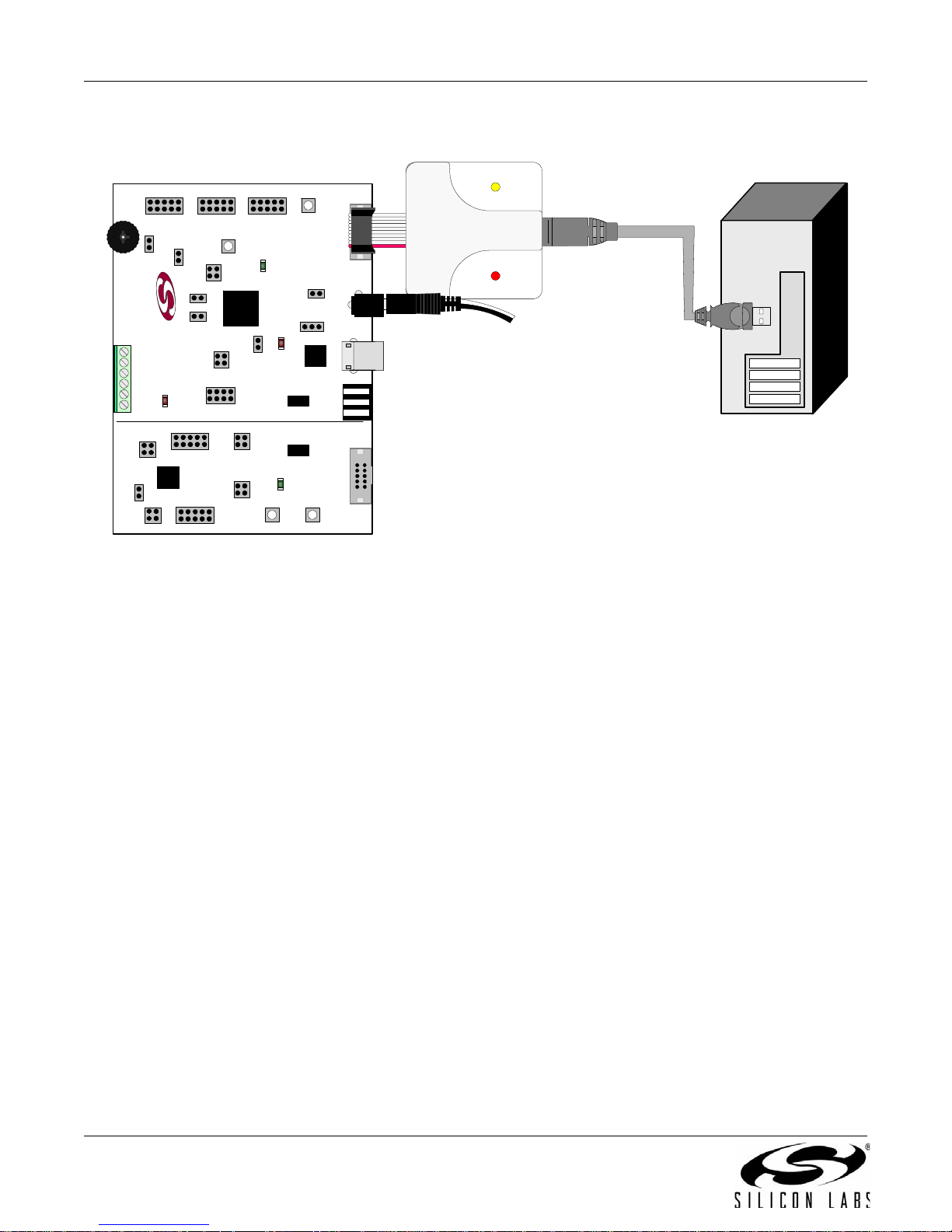
3. Hardware Setup
Refer to Figure 1 for a diagram of the hardware configuration .
1. Connect the USB Debug Adapter to the DEBUG A connector on the target board with the 10-pin ribbon cable.
2. Connect one end of the USB cable to the USB connector on the USB Debug Adapter.
3. Verify that shorting blocks are installed on the target board as shown in Figure 4 on page 9.
4. Connect the other end of the USB cable to a USB Port on the PC.
5. Connect the ac/dc power adapter to power jack P1 on the target board.
Notes:
•Use the Reset icon in the IDE to reset the target when connected during a debug session.
• Remove power from the target board and the USB Debug Adapter before connecting or disconnecting the
ribbon cable from the target board. Conn ecting or disconnecting the cable whe n the devices have power can
damage the device and/or the USB Debug Adapter.
Rev. 0.1 4/09 Copyright © 2009 by Silicon Laboratories C8051F540DK
Page 2
C8051F540DK
P1
P5
C8051F540-TB
P1.4_B
P1.4_A
Port 0 “A”
J1
Port 2 “A”
J3
Port 1 “A”
J2
+LIN_V
LIN_OUT
GND
DEBUG_A
P2
R22
SIDE “A”
SIDE “B”
DEBUG_B
P3
TB3
RESET_A
RESET_B
SILICON LABS
www.silabs.com
DS2
DS3
DS1
J13
J16
J17
J18
P4
J10 J9
J12
Port 0 “B”
J5
Port 1 “B”
J6
J4
F542
U2
C8051
F540
U1
J32
J7
Port 2 “B”
J11
J15
J8
J14
COMM
DS1
P1.3_A
PWR LED
P1.3_B
CP
2102
LIN
LIN
USB
Cable
AC/DC
Adapter
Target Board
Silicon Laboratories
USB DEBUG ADAPTER
Run
Stop Power
USB Debug
Adapter
TB1
Figure 1. Hardware Setup using a USB Debug Adapter
4. Software Installation
The included CD-ROM contains the Silicon Labs Integrated Development Environment (IDE), evaluation 8051
tools, optional software utilities, and additional documentation. Insert the CD-ROM into your PC’s CD-ROM drive.
An installer will automatically launch, allowing you to install the IDE software or read documentation by clicking
buttons on the Installation Panel. If the installer does not automatically start when you insert the CD-ROM, run
autorun.exe found in the root directory of the CD-ROM. Refer to the ReleaseNotes.txt file on the CD-ROM for the
latest information regarding known problems and restrictions.
4.1. System Requirements
The following are the system requirements necessary to run the debug and programming tools:
Pentium-class host PC running Microsoft Windows 2000 or newer.
One available USB port.
4.2. Development Tools Installation
To install the IDE, utilities, and code examples, perform the following steps:
1. Click on the "Install Development Tools" button on the installation utility's startup screen.
2. In the Kit Selection box that appears, choose the C8051F540DK development kit from the list of options.
3. In the next screen, choose “Components to be Installed” . The programs necessary to download and debug on
4. Installers selected in Step 3 will execute in sequence, prompting the user as they install programs,
2 Rev. 0.1
the MCU are the Silicon Labs IDE and the Keil 8051 Evaluation Toolset. The CP210x Drivers are necessary
to use the UART capabilities of the target board. See Section 4.3. for more information about installing the
CP210x drivers.
documentation, and drivers.
Page 3

C8051F540DK
4.3. CP210x USB to UART VCP Driver Installation
The C8051F540 Target Board includes a Silicon Laboratories CP2102 USB-to-UART Bridge Controller. Device
drivers for the CP2102 need to be installed before PC software such as HyperTerminal can communicate with the
target board over the USB connection. If the "Install CP210x Drivers" option is selected during installation, a driver
“unpacker” utility will launch.
1. Follow the steps to copy the driver files to the desired location. The default directory is C:\SiLabs\MCU\CP210x.
2. The final window will give an option to install the driver on the target system. Select the “Launch the CP210x VCP Driver
Installer” option if you are ready to install the driver.
3. If selected, the driver installer will now launch, providing an option to specify the driver installation location. After pressing
the “Install” button, the installer will search your system for copies of previously installed CP210x Virtual COM Port drivers. It
will let you know when your system is up to date. The driver files included in this installation have been certified by Microsoft.
4. If the “Launch the CP210x VCP Driver Installer” option was not selected in step 3, the installer can be found in the location
specified in step 2, by default C:\SiLabs\MCU\CP210x\Windows_2K_XP_S2K3_Vista. At this location, run
CP210xVCPInstaller.exe.
5. To complete the installation process, connect the included USB cable between the host computer and the USB connector
(P5) on the C8051F540 Target Board. Windows will automatically finish the driver installation. Information windows will pop
up from the taskbar to show the installation progress.
6. If needed, the driver files can be uninstalled by selecting “Silicon Laboratories CP210x USB to UART Bridge Driver
Removal” option in the “Add or Remove Programs” window.
5. Software Overview
The following software is necessary to build a project, download code to, and communicate with the target
microcontroller.
Silicon Labs Integrated Development Environment (IDE)
8051 Toolset
Other useful software that is provided on the development kit CD and the Silicon Labs Downloads
(www.silabs.com/mcudownloads) website includes the following:
Configuration Wizard 2
Keil µVision2 and µVision3 Drivers
MCU Production Programmer and Flash Programming Utilities
5.1. Silicon Labs IDE
The Silicon Labs IDE integrates a source-code editor, source-level debugger and in-system programmer. The use
of third-party compilers, assemblers, and linkers is also supported. This development kit includes evaluation
versions of commercial C compilers and assemblers which can be used from within the Silicon Labs IDE.
5.1.1. Third Party Toolsets
The Silicon Labs IDE has native support for many 8051 compilers. Natively-supported tools are as follows:
Keil
IAR
Raisonance
Tasking
Hi-Tech
SDCC
Specific instructions for integrating each of the supported tools can be found in the application notes section of the
CD, or on the Silicon Labs web site (http://www.silabs.com).
Rev. 0.1 3
Page 4

C8051F540DK
5.1.2. Getting Started With the Silicon Labs IDE
The following sections discuss how to open an example project in the IDE, build the source code, and download it
to the target device.
5.1.2.1. Running the F540_Blinky example program
The F540_Blinky example program blinks an LED on the target board.
1. Open the Silicon Labs IDE from the Start menu.
2. Select Project
3. Browse to the C:\SiLabs\MCU\Examples\C8051F54x\Blinky directory (default) and select the
F540_Blinky_C.wsp project file and click Open.
4. Once the project is open, build the project by clicking on the Build/Make Project button in the toolb ar or
selecting Project
Note: After the project has been built the first time, the Build/Make Project command will only build the
files that have been changed since the previous build. To rebuild all files and project dependencies, click
on the Rebuild All button in the toolbar or select Project
5. Before connecting to the target device, several connection optio ns may need to be set. Open th e Connec-
tion Options window by selecting Options
“USB Debug Adapter” option. Next, the correct “Debug Interface” must be selected. C8051F54x devices
use Silicon Labs “C2” 2-wire debug interface. Once all the selections are made, click the OK button to
close the window.
6. Click the Connect button in the toolbar or select Debug
device.
7. Download the project to the target by clicking the Download Code button in the toolbar.
Note: To enable automatic downloading if the program build is successful select Enable automatic con-
nect/download after build in the Project
build process, the IDE will not attempt the download.
8. Click on the Go button (green circle) in the toolbar or by selecting Debug
ning the firmware. The LED on the target board will start blinking.
Open Project to open an existing project.
Build/Make Project from the menu.
Rebuild All from the menu.
Connection Options... in the IDE menu. First, select the
Connect from the menu to connect to the
Target Build Configuration dialog. If errors occur dur ing th e
Go from the menu to start run-
5.1.2.2. Creating a New Project
Use the following steps to create a new projects. Once steps 1-5 in this section ar e complete, continue at Step 3 in
Section 5.1.2.1.
1. Select Project
2. Select File
ognized extension, such as .c, .h, or .asm, to enable color syntax highlighting.
3. Right-click on “New Project” in the Project Window. Select Add files to project. Select files in the file
browser and click Open. Continue adding files until all project files have been added.
4. For each of the files in the Project Window that you want assembled, compiled and linked into the target
build, right-click on the file name and select Add file to build. Each file will be assembled or compiled as
appropriate (based on file extension) and linked into the build of the absolute object file.
Note: If a project contains a large number of files, the “Group” feature of the IDE can be used to organize.
Right-click on “New Project” in the Project Window. Select Add Groups to project. Add pre-defined
groups or add customized groups. Right-click on the group name and choose Add file to group. Select
files to be added. Continue adding files until all project files have been added.
5. Save the project when finished with the debug session to preserve the current target build configuration,
editor settings and the location of all open debug views. To save the project, select Project
As... from the menu. Create a new name for the project and click on Save.
New Project to open a new project and reset all configuration settings to default.
New File to open an editor window. Create your source file(s) and save the fi le(s) with a rec-
Save Project
4 Rev. 0.1
Page 5
C8051F540DK
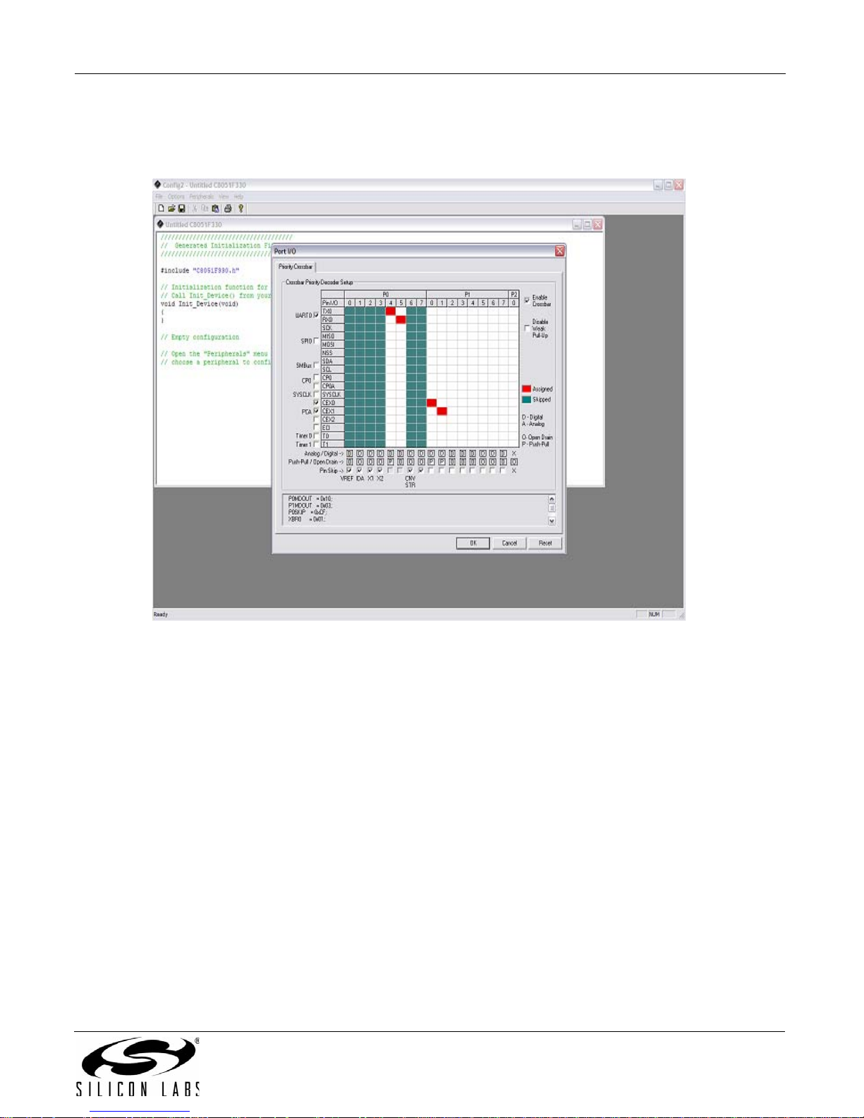
5.2. Configuration Wizard 2
The Configuration Wizard 2 is a code generation tool for all of the Silicon Laboratories devices. Code is generated
through the use of dialog boxes for each of the device's peripherals.
Figure 2. Configuration Wizard 2 Utility
The Configuration Wizard 2 utility helps accelerate development by automatically generating initialization source
code to configure and enable the on-chip resour ces needed b y most design project s. In just a few steps, th e wizard
creates complete startup code for a specific Silicon Laboratories MCU. The program is configurable to provide the
output in C or assembly. For more information, please refer to the Configuration Wizard 2 help available under the
Help menu in Configuration Wizard 2.
For more information, please refer to the Configuration Wizard 2 documentation. The documentation and software
are available from the Downloads webpage (www.silabs.com/mcudownloads).
5.3. Keil uVision2 and uVision3 Silicon Laboratories Drivers
As an alternative to the Silicon Laboratories IDE, the µVision debug driver allows the Keil µVision IDE to
communicate with Silicon Laboratories on-chip debug logic. In-system Flash memory programming integrated into
the driver allows for rapidly updating target code. The µVision IDE can be used to start and stop program
execution, set breakpoints, check variables, inspect and modify memory contents, and single-step through
programs running on the actual target hardware.
For more information, please refer to the uVision driver documentation. The documentation and software are
available from the Downloads webpage (www.silabs.com/mcudownloads).
Rev. 0.1 5
Page 6

C8051F540DK
5.4. Programming Utilities
The Silicon Labs IDE is the primary tool for downloading firmware to the MCU during development. There are two
software programming tools that are intended for use during prototyping or in the field: The MCU Production
Programmer and the Flash Programming Uti lities. The MCU Production Pro grammer is inst alled with the IDE to the
directory C:\Silabs\MCU\Utilities\Production Programmer\ (default). The Flash Programming Utilities can be
optionally installed from the CD and is installed to C:\Silabs\MCU\Utilities\FLASH Programming\ (default).
6. Example Source Code
Example source code and register definition files are provided in the “SiLabs\MCU\Examples\C8051F54x\”
directory during IDE installation. These files may be used as a template for code development. The comments in
each example file indicate which development tool chains were used when testing. Example applications include a
blinking LED example which configures the green LED on th e tar get board to blink at a fixed ra te. Also includ ed are
examples for each of peripherals of the MCU, suc h as the UART.
6.1. Register Definition Files
Register definition files C8051F540.inc, C8051F540_defs.h and compiler_defs.h define all SFR registers and bitaddressable control/status bits. These files are installed into the
“SiLabs\MCU\Examples\C8051F54x\Header_Files\” directory during IDE installation. The register and bit names
are identical to those used in the C8051F54x data sheet.
6.2. Blinking LED Example
The example source files F540_Blinky.asm and F540_Blinky.c installed in the default directory
“SiLabs\MCU\Examples\C8051F54x\Blinky” show examples of several basic C8051F540 functions. These include
disabling the watchdog timer (WDT), configuring the Port I/O crossbar, configuring a timer for an interrupt routine,
initializing the system clock, and configuring a GPIO port pin. When compiled/assembled and linked, this program
flashes the green LED on the C8051F540 Target Board about five times a second using the interrupt handler with
a C8051F540 timer.
6 Rev. 0.1
Page 7

C8051F540DK
7. Target Board
The C8051F540 Development Kit includes a target board with a C8051F540 (Side A) and C8051F542 (Sid e B)
device pre-installed for evaluation and preliminary sof tware development. Numerous input/output (I/O) connections
are provided to facilitate prototyping using the target board. Refer to Figure 3 for the locations of the various I/O
connectors. Figure 4 on page 9 shows the factory default shorting block positions. A summary of the signal names
and headers is provided in Table 9 on page 15.
P4 Header to choose between +5V from Debug Adapter (P2) or +5V from on-board regulator (U4)
J18 Connect V_HIGH node from TB1 LIN header to +5V regulator input for board power
P1 Power connector (accepts input from 7 to 15 VDC unregulated power adapter)
P5 USB connector (connects to PC for serial communication)
TB1 Shared LIN Connector for Side A and B MCUs for external nodes
J1-J3 Side A: Port 0 through Port 2 headers
J8 Side A: Connects +5V net to VIO and VREGIN of the MCU
J9, J10 Side A: External crystal enable connectors
J13 Side A: Connects decoupling capacitors C28 and C29 for MCU VREF (P0.0)
J15 Side A: Connects VIO to VIO_A_SRC which powers the R22 potentiometer, the RST_A
pin pull-up, and P1.4_A Switch pull-up.
J16 Side A: Connects P1.3_A LED and P1.4_A Switch to MCU port pins
J17 Side A: Connects MCU to two separate transceivers (UART(U3), and LIN(T2))
J20 Side A: Connects R27 potentiometer to port pin 1.2
P2 Side A: DEBUG connector for Debug Adapter interface
TB3 Side A: Power supply terminal block
J4 Side B: Connects +5V net to VIO and VREGIN of the MCU
J5-7 Side B: Port 0 through Port 2 headers
J11 Side B: Connects P1.3_B LED and P1.4_B Switch to MCU port pins
J12 Side B: Connects MCU to LIN transceiver (T1)
J19 Side B: Connects decoupling capacitors C41 and C42 for MCU VREF (P0.0)
P3 Side B: DEBUG connector for Debug Adapter interface
Rev. 0.1 7
Page 8

C8051F540DK
P1
P5
C8051F540-TB
P1.4_B
P1.4_A
Port 0 “A”
J1
Port 2 “A”
J3
Port 1 “A”
J2
+LIN_V
LIN_OUT
GND
DEBUG_A
P2
R22
SIDE “A”
SIDE “B”
DEBUG_B
P3
TB3
RESET_A
RESET_B
SILICON LABS
www.silabs.com
DS2
DS3
DS1
J13
J16
J17
J18
P4
J10 J9
J12
Port 0 “B”
J5
Port 1 “B”
J6
J4
F542
U2
C8051
F540
U1
J19
J7
Port 2 “B”
J11
J15
J8
J14
COMM
DS1
P1.3_A
PWR LED
P1.3_B
CP
2102
LIN
LIN
2
2
2
2
2
1
1
1
1
1
1
2
1
1
1
1
1
1
2
2
2
2
1
1
2
2
1
TB1
Figure 3. C8051F540 Target Board with Pin Numbers
8 Rev. 0.1
Page 9

C8051F540DK
P1
P5
C8051F540-TB
P1.4_B
P1.4_A
Port 0 “A”
J1
Port 2 “A”
J3
Port 1 “A”
J2
+LIN_V
LIN_OUT
GND
DEBUG_A
P2
R22
SIDE “A”
SIDE “B”
DEBUG_B
P3
TB3
RESET_A
RESET_B
SILICO N LABS
www.silabs.com
DS2
DS3
DS1
J13
J16
J17
J18
P4
J10 J9
J12
Port 0 “B”
J5
Port 1 “B”
J6
J4
F542
U2
C8051
F540
U1
J19
J7
Port 2 “B”
J11
J15
J8
J14
COMM
DS1
P1.3_A
PWR LED
P1.3_B
CP
2102
LIN
LIN
TB1
7.1. Target Board Shorting Blocks: Factory Defaults
The C8051F540 T arget Board comes from the factory with pre-installed shorting blocks on many headers. Figure 4
shows the positions of the factory default shorting blocks.
Figure 4. C8051F540 Target Board Shorting Blocks: Factory Defaults
Rev. 0.1 9
Page 10

C8051F540DK
7.2. Target Board Power Options and Current Measurement (J4, J8, J24, P1, TB1)
The MCUs on the C8051F540 Target Board are powered from a +5 V net. The +5 V net is connected to the
headers J8 (Side A) and J4 (Side B). Shorting blocks can be put on each header to connect the +5 V net to the
VREGIN and VIO pins on the two MCUs. With the shorting blocks removed, a source meter can be used across
the headers to measure the current consumption of the MCU.
The +5 V net on the target board has three possible sources:
1. 12 V dc power using the ac to dc power adapter (P1)
2. 5 V dc USB VBUS power from PC via the USB Debug Adapter (DEBUG_A)
3. 12 V dc power from the LIN external header (TB1)
7.2.1. Using the AC to DC Power Adapter as the Target Board Power Source (P1, P4)
The default configuration of the target board uses the ac to dc power adapter as the source. The 12 V from the
adapter is regulated to +5 V using an LDO regulator (U4). The output of the regulator is connected to the +5 V net
of the target board through the P4 header. A shorting block should be installed on pins P4[2–3] for this purpose.
The +5 V net powers the MCUs.
7.2.2. Using the USB Debug Adapter as the Target Board Power Source (P4)
The target board can use +5 V provided by the USB Debug Adapter. To enable this source, a shorting block should
be installed on pins P4[1-2]. With this shorting block, the output of the LDO regulator (U4) is disconnected from the
+5 V net of the target board, and the SER_PWR node is connected to +5 V.
Note: The USB Debug Adapter does not provide the necessary peak power for the CAN transceivers to operate.
One of the 12 V dc sources is recommended for CAN transceiver operation.
7.2.3. Using an External +12V LIN Source as the Target Board Power Source (P4, TB1)
The two 12 V power sources (LIN and ac to dc power ad apter) are ORed toge ther using reverse-bia sed di odes (Z1
and Z2) and connected to the input of the LDO regulator (U6). The output of the regulator is connected to the +5 V
net of the target board through the P4 header. A shorting block should be installed on pins P4[2-3] for this purpose.
The +5 V net powers the MCUs directly.
7.3. System Clock Sources (J9, J10)
7.3.1. Internal Oscillators
The C8051F540 and C8051F542 devices installed on the target board feature a factory-calibrated, programmable
high-frequency internal oscillator (24 MHz base frequency , ±0.5%), which is enabled as the system clock source on
reset. After reset, the internal oscillator operates at a frequency of 187.5 kHz by default but may be configured by
software to operate at other frequencies. The on-chip crystal is accurate for LIN master communications and in
many applications an external oscillator is not required. However, if you wish to operate the C8051F540 device
(Side A) at a frequency not available with the internal oscillator, an external crystal may be used. Refer to the
C8051F54x data sheet for more information on configuring the system clock source.
7.3.2. External Oscillator Options
The target board is designed to facilitate the installation of an external crystal. Remove shorting blocks at headers
J9 and J10 and install the crystal at the pa ds marked Y1. Install a 10 M resistor at R2 and install capacitors at C7
and C8 using values appropriate for the crystal you select. If you wish to operate the external oscillator in capacitor
or RC mode, options to install a capacitor or an RC network are also available on the t arge t board. R2, R3, C7, and
C8 are located on the back side of the board, n ear the Side A MCU. Po pulate C7 fo r ca p a citor mo de, a nd popula te
R3 and C7 for RC mode. Refer to the C8051F54x data sheet for more information on the use of external
oscillators.
10 Rev. 0.1
Page 11

C8051F540DK
7.4. Switches and LEDs (J11, J16)
Two push-button switches are provided on the target board for each MCU. Switch RESET_A is connected to the
pin of the C8051F540. Switch RESET_B is connected to the RST pin of the C8051F542. Pressing RESET_A
RST
puts the C8051F540 device into its hardware-reset state, and similarly for RESET_B and the C8051F542 MCU.
Switches P1.4_A and P1.4_B are connected to the MCU’s general purpose I/O (GPIO) pins through headers.
Pressing either one of these switches generates a logic low signal on the port pin. Remove the shorting block from
the header to disconnect these switches from the port pins. See Table 1 for the port pins and headers
corresponding to each switch.
Four LEDs are provided on the target board to serve as indicators. The red LED labeled PWR indicates presence
of power to the target board. The second red LED labeled COMM indicates if the CP2102 USB-to-U ART bridge is
recognized by the PC. The green LED on Side A is labeled with port pin name and is connected to a C8051F580
GPIO pin through a header. Remove the shorting block from the header to disconnect the LED from the port pin.
Similarly, a second green LED on Side B is connected to the C8051F542 through another header. See Table 1 for
the port pins and headers corresponding to each LED.
Table 1. Target Board I/O Descriptions
Description I/O Header(s)
RESET_A Reset (Side A) none
RESET_B Reset (Side B) none
P1.4_A Switch P1.4 (Side A) J16[1–2]
P1.4_B Switch P1.4 (Side B) J11[1–2]
P1.3_A LED P1.3 (Side A) J16[3–4]
P1.3_B LED P1.3 (Side B) J11[3–4]
Red LED (PWR) Power none
Red LED (COMM) COMM Active none
7.5. Target Board Debug Interfaces (P2 and P3)
The
debug
connectors P2 (DEBUG_A) and P3 (DEBUG_B) provide access to the
debug
C8051F540 and C8051F542. The
Adapter to the target board for in-circuit debugging and Flash programming. Table 2 shows the
definitions.
connectors are used to connect the Serial Adapter or the USB Debug
Table 2. DEBUG Connector Pin Descriptions
Side A - C8051F540 Side B - C8051F542
Pin # Description Pin # Description
1 Not Connected 1 Not Connected
2, 3, 9 GND (Ground) 2, 3, 9 GND (Ground)
4 P2.1_C2D_A 4 P2.1_C2D_B
5RST_A
6P2.1 6P2.1_B
7RST
8 Not Connected 8 Not Connected
10 USB Power (+5VDC from P2) 10 Not Connected
(Reset) 5 RST_B (Reset)
/C2CK_A 7 RST/C2CK_B
debug
(C2) pins of the
DEBUG
pin
Rev. 0.1 11
Page 12

C8051F540DK
7.6. Serial Interface (P5, J14)
A USB-to-UART bridge device (U3) and USB connector (P5) are provided on the target board to facilitate serial
connections to UART0 of the C8051F540 (Side A). The Silicon Labs CP2102 USB-to-UART bridge provides data
connectivity between the C8051F540 and the PC via a USB port. The TX and RX signals of UART0 may be
connected to the CP2102 by installing shorting blocks on header J14. The shorting block positions for connecting
each of these signals to the CP2102 are listed in Table 3. To use this interface, the USB-to-UART device drivers
should be installed as described in Section 4.3. "CP210x USB to UART VCP Driver Installation‚" on page 3.
Table 3. Serial Interface Header (J14) Description
Header Pins UART0 Pin Description
J14[3–4] UART_TX (P0.4_A)
J14[1–2] UART_RX (P0.5_A)
7.7. LIN Interface and Network (J12, J14, TB1)
Both MCUs on the target board are connected to LIN transceivers through headers. These headers assume that
the MCU’s crossbars are configured to put the LIN TX an d RX pins on port pins P1.0 and P1.1 respectively. See
the C8051F54x data sheet for crossbar configuration. The C8051F540 (Side A) is connected to the T1 transceiver
through the J14 header and the C8051F542 (Side B) is connected to the T2 transceiver through the J12 header.
The two LIN transceivers are connected to each other and form a LIN network. Other external devices can be
connected to the LIN network through the TB1 interface. The TB1 interface also provides the option for connecting
an external power source so that all LIN transceivers can use the same source voltage. This source voltage can
also be used to power the target board. If an external voltage source is not provided, the LIN transceivers use the
12 V provided through the P1 power adapter connector. See Section 7.2. for more power option details. The
shorting block positions for connecting the MCUs to the LIN transceivers are listed in Table 4. The pin connections
for the external LIN devices are listed in Table 5.
Table 4. LIN Interface Headers (J12 and J14) Description
Header Pins LIN0 Pin Description
J14[5–6] LIN_TX (P1.0_A)
J14[7–8] LIN_RX (P1.1_A)
J12[3–3] LIN_TX (P1.0_B)
J12[1–2] LIN_RX (P1.1_B)
Table 5. TB1 External LIN Interface Header Description
Pin # Pin Description
1GND
2LIN_OUT
3+LIN_V
12 Rev. 0.1
Page 13

C8051F540DK
7.8. Port I/O Connectors (J1-J3 and J5-J7)
Each of the parallel ports of the C8051F540 (Side A) and C8051F542 (Side B) has its own 10-pin header
connector. Each connector provides a pin for the corresponding port pins 0–7, +5 V VIO, and digital ground. The
same pin-out is used for all of the port connectors.
Table 6. Port I/O Connector Pin Description
Pin # Pin Description
1Pn.0
2Pn.1
3Pn.2
4Pn.3
5Pn.4
6Pn.5
7Pn.6
8Pn.7
9 +5V (VIO)
10 GND (Ground)
Port 2 on the C8051F542 (Side B) MCU has only two pins and has a reduced header.
Table 7. Port I/O Connector Pin Description (J7)
Pin # Pin Description
1Pn.0
2Pn.1
3 +5V (VIO)
4 GND (Ground)
7.9. Voltage Reference (VREF) Connectors (J13 and J19)
The VREF connectors can be used to connect the VREF pin from the MCU (P0.0) to external 0.1 µF and 4.7 µF
decoupling capacitors. The C8051F540 (Side A) de vice is con nected to the capacitors through the J13 header and
the C8051F542 (Side B) device connects to its own set of capacitors through J19.
7.10. Potentiometer (J17)
The C8051F540 (Side A) device has the option to connect port pin P1.2 to a 10K linear potentiometer. The
potentiometer is connected through the J17 header. The potentiometer can be used for testing the analog-to-digital
(ADC) converter of the MCU.
Rev. 0.1 13
Page 14

C8051F540DK
7.11. Power Supply I/O (Side A) (TB3)
All of the C8051F540 target device’s supply pins are connected to the TB3 terminal block. Refer to Table 8 for the
TB3 terminal block connections.
Table 8. TB3 Terminal Block Pin Descriptions
Pin # Description
1VIO_A
2 VREGIN_A
3 VDD_A
4VDDA_A
5GNDA_A
6GND
7.12. Alternate Power Supply Headers (J15, J18)
The C8051F540 Target Board includes two headers that allow for alternate power sources and power
measurement. Header J15 connects the VIO volt age supp lied to the Side A MCU to other perip herals on the boar d,
such as the P1.4_SW push-button switch pull-up, and the R17 potentiometer source. To enable current
measurement, the shorting block on J15 can be removed so that the VIO_A node only powers the VIO pin on the
MCU. Another voltage source will need to be applied to the VIO_SRC node to power the other peripherals.
Header J18 connects the P4 power-adapter supply to the V_HIGH node, which is used as the power sour ce for the
LIN transceivers (T1, T2). The shorting block on header J18 can be removed to force the LIN transceivers to use
the voltage supply externally supplied on the +LIN_V pin on the TB1 header.
7.13. C2 Pin Sharing
On the C8051F540 (Side A), the debug pins C2CK and C2D are shared with the pins RST and P2.1, respectively.
On the C8051F542 (Side B), the debug pins C2CK and C2D are shared with the pins RST
The target board includes the resistors necessary to enable pin sharing which allow the pin–shared pins (RST
P3.0) to be used normally while simultaneously debugging the device. See Application Note “AN124: Pin Sharing
Techniques for the C2 Interface” at www.silabs.com for more information regarding pin sharing.
and P2.1, respectively.
and
14 Rev. 0.1
Page 15

C8051F540DK
7.14. Target Board Pin Assignment Summary
Some GPIO pins of the C8051F540 MCU can have an alternate fixed function. For example, pin 30 on the
C8051F540 MCU is designated P0.4, and can be used as a GPIO pin. Also, if the UAR T0 periphe ral on the MCU is
enabled using the crossbar registers, the TX signal is routed to this pin. This is shown in the "Alternate Fixed
Function" column. The "Target Board Function" column shows that this pin is used as TX on the C8051F540 Target
Board. The "Relevant Headers" column sho ws that th is signal is routed to pin 6 of the J14 header and pin 6 of the
J1 header. More details can be found in the C8051F54x data sheet. Some of the GPIO pins of the C8051F540
have been used for various functions on the target board. Table 9 summarizes the C8051F540 MCU (Side A) pin
assignments on the target board, and also shows the various headers associated with each signal.
Table 9. C8051F540 Target Board Pin Assignments and Headers
MCU Pin Name Pin# Primary
Function
P0.0 8 P0.0 VREF VREF J1[1], J13[1]
P0.1 1 P0.1 CNVSTR CNVSTR J1[2]
P0.2 32 P0.2 XTAL1 XTAL1 J1[3]*, J9[2]
P0.3 31 P0.3 XTAL2 XTAL2 J1[4]*, J10[2]
P0.4 30 P0.4 UART_TX TX_MCU J1[5], J14[6]
P0.5 29 P0.5 UART_RX RX_MCU J1[6], J14[8]
P0.6 28 P0.6 J1[7]
P0.7 27 P0.7 J1[8]
P1.0 26 P1.0 LIN_TX J2[1], J14[4]
P1.1 25 P1.1 LIN_RX J2[2], J14[2]
P1.2 24 P1.2 POTENTIOMETER J2[3], J17[2]
P1.3 23 P1.3 LED J2[4], J16[1]
P1.4 22 P1.4 SWITCH J2[5], J16[3]
P1.5 21 P1.5 GPIO J2[6]
Alternate Fixed
Function
Target Board
Function
Relevant Headers
P1.6 20 P1.6 GPIO J2[7]
P1.7 19 P1.7 GPIO J2[8]
P2.0 18 P2.0 GPIO J3[1]
P2.1 17 P2.1 GPIO J3[2]
P2.2 16 P2.2 GPIO J3[3]
P2.3 15 P2.3 GPIO J3[4]
P2.4 14 P2.4 GPIO J3[5]
P2.5 13 P2.5 GPIO J3[6]
P2.6 12 P2.6 GPIO J3[7]
P2.7 11 P2.7 GPIO J3[8]
Rev. 0.1 15
Page 16

C8051F540DK
Table 9. C8051F540 Target Board Pin Assignments and Headers (Continued)
MCU Pin Name Pin# Primary
Function
P3.0 9 P3.0 C2D Test Point near P2
/C2CK 12 RST C2CK RST/C2CK P2[7], P2[5]*
RST
VIO 2 VIO VIO J8[1], J15[2], TB3[1]
VREGIN 3 VREGIN VREGIN J8[3], TB3[2]
VDD 4 VDD VDD TB3[3]
VDDA 5 VDDA VDDA TB3[4]
GND 6 GND GND J1-J3[1], TB3[6]
GNDA 7 GNDA VDD TB3[5]
*Note: Headers denoted by this symbol are not directly connected to the MCU pin; the connection might be via one or more
headers and/or pin-sharing resistor(s). See board schematic for details.
Alternate Fixed
Function
Target Board
Function
Relevant Headers
J1-J3[2]
16 Rev. 0.1
Page 17

8. Schematics
C8051F540DK
Figure 5. C8051F540 Target Board Schematic (Page 1 of 4)
Rev. 0.1 17
Page 18

C8051F540DK
18 Rev. 0.1
Figure 6. C8051F540 Target Board Schematic (Page 2 of 4)
Page 19

C8051F540DK
Figure 7. C8051F540 Target Board Schematic (Page 3 of 4)
Rev. 0.1 19
Page 20

C8051F540DK
20 Rev. 0.1
Figure 8. C8051F540 Target Board Schematic (Page 4 of 4)
Page 21

NOTES:
C8051F540DK
Rev. 0.1 21
Page 22

C8051F540DK
The information in this document is believed to be accurate in all respects at the time of publication but is subject to change without notice.
Silicon Laboratories assumes no responsibility for errors and omissions, and disclaims responsibility for any consequences resulting from
the use of information included herein. Additionally, Silicon Laboratories assumes no responsibility for the functioning of undescribed features
or parameters. Silicon Laboratories reserves the right to make changes without further notice. Silicon Laboratories makes no warranty, representation or guarantee regarding the suitability of its products for any particular purpose, nor does Silicon Laboratories assume any liability
arising out of the application or use of any product or circuit, and specifically disclaims any and all liability, including without limitation consequential or incidental damages. Silicon Laboratories products are not designed, intended, or authorized for use in applications intended to
support or sustain life, or for any other application in which the failure of the Silicon Laboratories product could create a situation where personal injury or death may occur. Should Buyer purchase or use Silicon Laboratories products for any such unintended or unauthorized application, Buyer shall indemnify and hold Silicon Laboratories harmless against all claims and damages.
CONTACT INFORMATION
Silicon Laboratories Inc.
400 West Cesar Chavez
Austin, TX 78701
Tel: 1+(512) 416-8500
Fax: 1+(512) 416-9669
Toll Free: 1+(877) 444-3032
Please visit the Silicon Labs Technical Support web page:
https://www.silabs.com/support/pages/contacttechnicalsupport.aspx
and register to submit a technical support request.
Silicon Laboratories and Silicon Labs are trademarks of Silicon Laboratories Inc.
Other products or brandnames mentioned herein are trademarks or registered trademarks of their respective holders.
22 Rev. 0.1
 Loading...