

Page 1
C8051F410/1/2/3
2.0 V, 32/16 kB Flash, smaRTClock, 12-bit ADC
Analog Peripherals
- 12-Bit ADC
• ±1 LSB INL; no missing codes
• Programmable throughput up to 200 ksps
• Up to 24 external inputs
• Data dependent windowed interrupt generator
• Built-in temperature sensor (±3 °C)
-
Two 12-Bit Current Mode DACs
- Two Comparators
• Programmable hysteresis and response time
• Configurable as wake-up or reset source
- POR/Brownout Detector
- Voltage Reference—1.5, 2.2 V (programmable)
On-Chip Debug
- On-chip debug circuitry facilitates full-speed, non-
intrusive in-system debug (No emulator required)
- Provides breakpoints, single stepping
- Inspect/modify memory and registers
- Complete development kit
Supply Voltage 2.0 to 5.25 V
- Built-in LDO regulator: 2.1 or 2.5 V
High Speed 8051 µC Core
- Pipelined instruction architecture; executes 70% of
instructions in 1 or 2
system clocks
- Up to 50 MIPS throughput with
50 MHz system clock
- Expanded interrupt handler
Memory
- 2304 bytes internal data RAM (256 + 2048)
- 32/16 kB Flash; In-system programmable in
byte sectors
512
- 64 bytes battery-backed RAM (smaRTClock)
Digital Peripherals
- 24 port I/O; push-pull or open-drain, up to 5.25 V
tolerance
- Hardware SMBus™ (I2C™ Compatible), SPI™, and
UART serial ports available concurrently
- Four general purpose 16-bit counter/timers
- Programmable 16-bit counter/timer array with six
capture/compare modules, WDT
- Hardware smaRTClock operates down to 1 V with
64 bytes battery-backed RAM and backup voltage
regulator
Clock Sources
- Internal oscillators: 24.5 MHz 2% accuracy supports
UART operation; clock multiplier up to 50
MHz
- External oscillator: Crystal, RC, C, or Clock
(1 or 2 pin modes)
- smaRTClock oscillator: 32 kHz Crystal or
self-resonant oscillator
- Can switch between clock sources on-the-fly
32-PIN LQFP or 28-PIN 5x5 QFN
Temperature Range: –40 to +85 °C
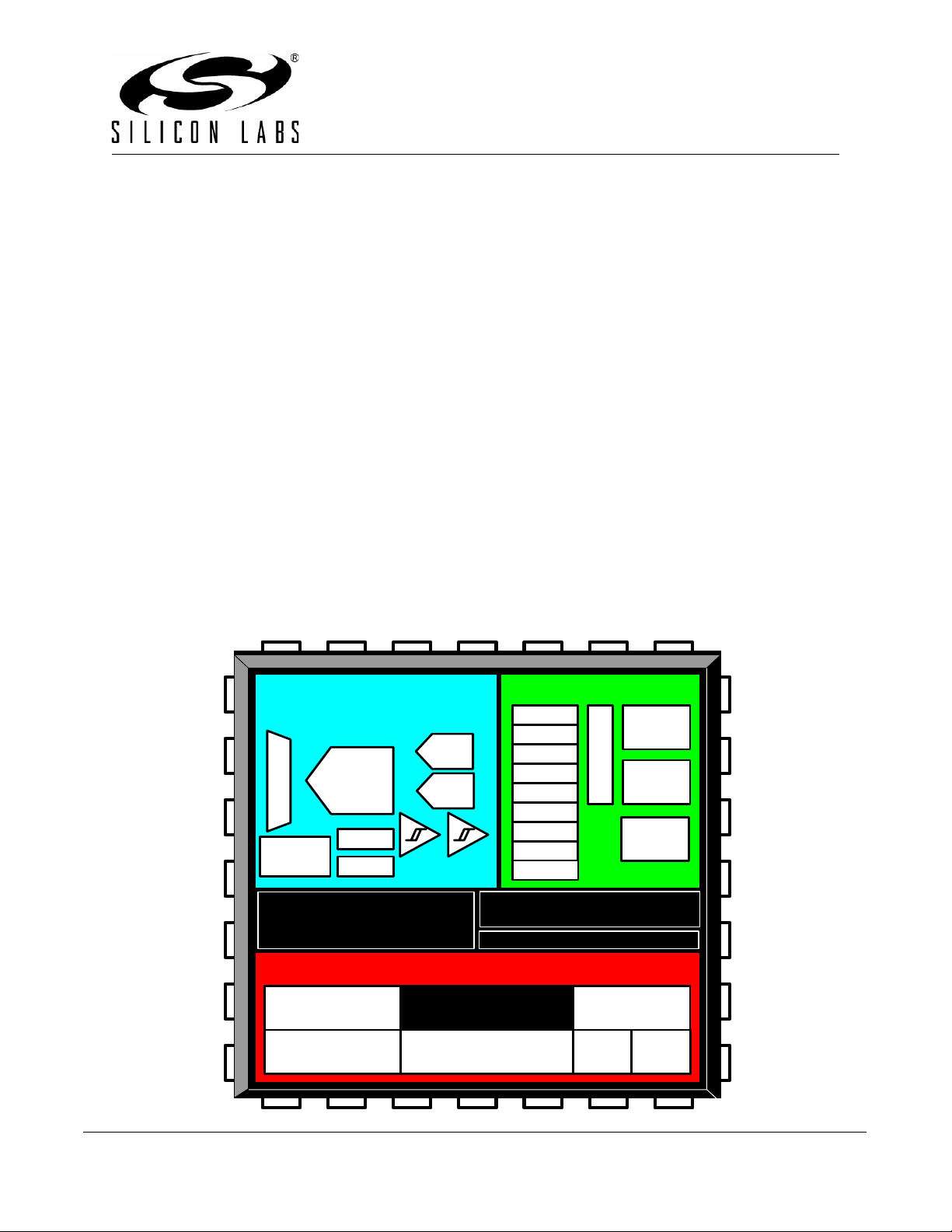
ANALOG
PERIPHERALS
A
M
U
X
TEMP
SENSOR
24.5 MHz PRECISION
INTERNAL OSCILLATOR
WITH CLOCK MULTIPLIER
32/16 kB
ISP FLASH
FLEXIBLE
INTERRUPTS
12-bit
200 ksps
ADC
+
VREF
VREG
-
VOLTAGE
COMPARATORS
HIGH-SPEED CONTROLLER CORE
12-bit
IDAC
12-bit
IDAC
+
-
SMBus
Timer 0
Timer 1
Timer 2
Timer 3
INTERNAL OSCILLATOR
HARDWARE smaRTClock
8051 CPU
(50 MIPS)
DEBUG
CIRCUITRY
DIGITAL I/O
UART
SPI
PCA
CRC
LOW FREQUENCY
POR
Port 0
Port 1
CROSSBAR
Port 2
2368 B
SRAM
WDT
Rev. 1.0 2/07 Copyright © 2007 by Silicon Laboratories C8051F41x
Page 2

C8051F410/1/2/3
NOTES:
2 Rev. 1.0
Page 3

C8051F410/1/2/3
Table of Contents
1. System Overview.................................................................................................... 19
1.1. CIP-51™ Microcontroller................................................................................... 25
1.1.1. Fully 8051 Compatible Instruction Set...................................................... 25
1.1.2. Improved Throughput............................................................................... 25
1.1.3. Additional Features. ..... ..... ............................ .... ..... ..... ............................ . 25
1.2. On-Chip Debug Circuitry................................................................................... 26
1.3. On-Chip Memory............................................................................................... 27
1.4. Operating Modes.... ..... .... ............................ ..... ..... ............................ .... ........... 28
1.5. 12-Bit Analog to Digital Converter..................................................................... 29
1.6. Two 12-bit Current-Mode DACs.................................................... ..... .... ..... ...... 29
1.7. Programmable Comparators............................................................................. 30
1.8. Cyclic Redundancy Check Unit......................................................................... 31
1.9. Voltage Regulator............................................................................................. 31
1.10.Serial Ports................................ .... ............................ ..... ..... .... ......................... 31
1.11.smaRTClock (Real Time Clock)....................................................................... 32
1.12.Port Input/Output.............................................................................................. 33
1.13.Programmable Counter Array........................................................................... 34
2. Absolute Maximum Ratings .................................................................................. 35
3. Global DC Electrical Characteristics.................................................................... 36
4. Pinout and Package Definitions............................................................................ 41
5. 12-Bit ADC (ADC0).................................................................................................. 51
5.1. Analog Multiplexer............................................................................................ 51
5.2. Temperature Sensor......................................................................................... 52
5.3. ADC0 Operation................................................................................................ 52
5.3.1. Starting a Conversion............................................................................... 53
5.3.2. Tracking Modes........................................................................................ 53
5.3.3. Timing....................................................................................................... 54
5.3.4. Burst Mode...............................................................................................56
5.3.5. Output Conversion Code.......................................................................... 57
5.3.6. Settling Time Requirements..................................................................... 58
5.4. Programmable Window Detector...................................................................... 63
5.4.1. Window Detector In Single-Ended Mode................................................. 66
6. 12-Bit Current Mode DACs (IDA0 and IDA1)........................................................ 69
6.1. IDAC Output Scheduling............................................ ..... ............................ ..... . 69
6.1.1. Update Output On-Demand..................................................................... 69
6.1.2. Update Output Based on Timer Overflow ................................................70
6.1.3. Update Output Based on CNVSTR Edge................................................. 70
6.2. IDAC Output Mapping................................................ ............................ ..... ..... . 70
6.3. IDAC External Pin Connections........................................................................ 73
7. Voltage Reference.................................................................................................. 77
8. Voltage Regulator (REG0)...................................................................................... 81
9. Comparators ......................................................................................................... 83
Rev. 1.0 3
Page 4

C8051F410/1/2/3
10.CIP-51 Microcontroller........................................................................................... 93
10.1.Instruction Set................................................................................................... 94
10.1.1.Instruction and CPU Timing..................................................................... 94
10.1.2.MOVX Instruction and Program Memory................................................. 95
10.2.Register Descriptions....................................................................................... 98
10.3.Power Management Modes............................................................................101
10.3.1.Idle Mode............................................ ..... ..... .... ............................ ..... ....102
10.3.2.Stop Mode.............................................................................................. 102
10.3.3.Suspend Mode....................................................................................... 102
11.Memory Organization and SFRs......................................................................... 103
11.1.Program Memory............................................................................................ 103
11.2.Data Memory.................................................................................................. 104
11.3.General Purpose Registers................................................. .... ..... ..... ............. 104
11.4.Bit Addressable Locations....................... .... ............................ ..... ..... .... ......... 104
11.5.Stack............................................................................................................... 104
11.6.Special Function Registers............................................................................. 105
12.Interrupt Handler ........................ ..... .... ............................ ..... ..... .... ....................... 110
12.1.MCU Interrupt Sources and Vectors............ ..... ............................ ..... .... ..... ....110
12.2.Interrupt Priorities........................................................................................... 110
12.3.Interrupt Latency............................................................................................. 110
12.4.Interrupt Register Descriptions....................................................................... 112
12.5.External Interrupts................................................. .... ..... ............................ ....117
13.Prefetch Engine................................................. ..... ..... ............................ .... ..... .... 119
14.Cyclic Redundancy Check Unit (CRC0) ............................................................. 121
14.1.CRC Algorithm......................................... .... ..... ..... ............................ .... ..... ....121
14.2.Preparing for a CRC Calculation.................................................................... 123
14.3.Performing a CRC Calculation....................................................................... 123
14.4.Accessing the CRC0 Result...........................................................................123
14.5.CRC0 Bit Reverse Feature............................................................................. 123
15.Reset Sources....................................................................................................... 127
15.1.Power-On Reset............................................................................................. 128
15.2.Power-Fail Reset / VDD Monitor .................................................................... 129
15.3.External Reset....................................................... .... ..... ............................ ....130
15.4.Missing Clock Detector Reset........................................................................ 130
15.5.Comparator0 Reset........................................................................................ 130
15.6.PCA Watchdog Timer Reset ..........................................................................131
15.7.Flash Error Reset........................................................................................... 131
15.8.smaRTClock (Real Time Clock) Reset........................................................... 132
15.9.Software Reset............................................................................................... 132
16.Flash Memory ....................................................................................................... 135
16.1.Programming The Flash Memory................................................................... 135
16.1.1.Flash Lock and Key Functions............................................................... 135
16.1.2.Flash Erase Procedure.......................................................................... 135
16.1.3.Flash Write Procedure........................................................................... 136
16.2.Non-volatile Data Storage......................................... ..... ..... ........................... 137
4 Rev. 1.0
Page 5

C8051F410/1/2/3
16.3.Security Options............................................................................................. 137
16.4.Flash Write and Erase Guidelines.................................................................. 139
16.4.1.VDD Maintenance and the VDD Monitor............................................... 139
16.4.2.16.4.2 PSWE Maintenance.................................................................... 140
16.4.3.System Clock........................ ..... ............................ ..... .... ..... .................. 140
16.5.Flash Read Timing......................................................................................... 142
17.External RAM........................................................................................................ 145
18.Port Input/Output............................. .... ..... ............................ ..... .... ..... .................. 147
18.1.Priority Crossbar Decoder.............................................................................. 149
18.2.Port I/O Initialization....................................................................................... 151
18.3.General Purpose Port I/O................................. ..... .... ............................ ..... ....154
19.Oscillators............................................................................................................. 165
19.1.Programmable Internal Oscillator...................................................................165
19.1.1.Internal Oscillator Suspend Mode.......................................................... 166
19.2.External Oscillator Drive Circuit...................................................................... 168
19.2.1.Clocking Timers Directly Through the External Oscillator...................... 168
19.2.2.External Crystal Example....................................................................... 168
19.2.3.External RC Example............................................................................. 170
19.2.4.External Capacitor Example................................................................... 170
19.3.Clock Multiplier............................................................................................... 172
19.4.System Clock Selection.................................................................................. 174
20.smaRTClock (Real Time Clock)........................................................................... 177
20.1.smaRTClock Interface.................................................................................... 178
20.1.1.smaRTClock Lock and Key Functions................................................... 178
20.1.2.Using RTC0ADR and RTC0DAT to Access
smaRTClock Internal Registers.............................................................. 178
20.1.3.smaRTClock Interface Autoread Feature............................................... 178
20.1.4.RTC0ADR Autoincrement Feature.........................................................179
20.2.smaRTClock Clocking Sources...................................................................... 182
20.2.1.Using the smaRTClock Oscillator in Crystal Mode................................ 182
20.2.2.Using the smaRTClock Oscillator in Self-Oscillate Mode ...................... 182
20.2.3.Automatic Gain Control (Crystal Mode Only)....................... ..... ............. 183
20.2.4.smaRTClock Bias Doubling...................................................................183
20.2.5.smaRTClock Missing Clock Detector..................................................... 183
20.3.smaRTClock Timer and Alarm Function......................................................... 185
20.3.1.Setting and Reading the smaRTClock Timer Value............................... 185
20.3.2.Setting a smaRTClock Alarm...................................... .... ....................... 186
20.4.Backup Regulator and RAM........................................................................... 187
21.SMBus ................................................................................................................... 191
21.1.Supporting Documents................................................................................... 192
21.2.SMBus Configuration......................................................................................192
21.3.SMBus Operation........................................................................................... 192
21.3.1.Arbitration...............................................................................................193
21.3.2.Clock Low Extension.............................................................................. 193
21.3.3.SCL Low Timeout................................................................................... 194
Rev. 1.0 5
Page 6

C8051F410/1/2/3
21.3.4.SCL High (SMBus Free) Timeout.......................................................... 194
21.4.Using the SMBus.............................................. ............................ ..... .... ..... ....194
21.4.1.SMBus Configuration Register............................... ..... ........................... 195
21.4.2.SMB0CN Control Register..................................................................... 198
21.4.3.Data Register........................ ............................ ..... ..... .... ....................... 201
21.5.SMBus Transfer Modes.................................................................................. 201
21.5.1.Master Transmitter Mode....................................................................... 201
21.5.2.Master Receiver Mode........................................................................... 202
21.5.3.Slave Receiver Mode.............................................................................203
21.5.4.Slave Transmitter Mode......................................................................... 204
21.6.SMBus Status Decoding.................................................................................204
22.UART0.................................................................................................................... 207
22.1.Enhanced Baud Rate Generation................................................................... 208
22.2.Operational Modes................................................ .... ..... ..... ...........................209
22.2.1.8-Bit UART............................................................................................. 209
22.2.2.9-Bit UART............................................................................................. 210
22.3.Multiprocessor Communications.................................................................... 210
23.Enhanced Serial Peripheral Interface (SPI0)...................................................... 217
23.1.Signal Descriptions.........................................................................................218
23.1.1.Master Out, Slave In (MOSI).................................................................. 218
23.1.2.Master In, Slave Out (MISO).................................................................. 218
23.1.3.Serial Clock (SCK)................................................................................. 218
23.1.4.Slave Select (NSS)................................................................................ 218
23.2.SPI0 Master Mode Operation ......................................................................... 219
23.3.SPI0 Slave Mode Operation........................................................................... 220
23.4.SPI0 Interrupt Sources................................................................................... 221
23.5.Serial Clock Timing........................ ..... ..... .... ..... ............................ ..... .... ..... ....221
23.6.SPI Special Function Registers......................................................................222
24.Timers.................................................................................................................... 231
24.1.Timer 0 and Timer 1....................................................................................... 231
24.1.1.Mode 0: 13-bit Counter/Timer................................................................ 231
24.1.2.Mode 1: 16-bit Counter/Timer................................................................ 233
24.1.3.Mode 2: 8-bit Counter/Timer with Auto-Reload...................................... 233
24.1.4.Mode 3: Two 8-bit Counter/Timers (Timer 0 Only)................................. 234
24.2.Timer 2 ..........................................................................................................239
24.2.1.16-bit Timer with Auto-Reload................................................................ 239
24.2.2.8-bit Timers with Auto-Reload................................................................240
24.2.3.External/smaRTClock Capture Mode..................................................... 241
24.3.Timer 3 ..........................................................................................................244
24.3.1.16-bit Timer with Auto-Reload................................................................ 244
24.3.2.8-bit Timers with Auto-Reload................................................................245
24.3.3.External/smaRTClock Capture Mode..................................................... 246
25.Programmable Counter Array (PCA0)................................................................ 249
25.1.PCA Counter/Timer................................. .... ............................ ..... ..... .... ......... 250
25.2.Capture/Compare Modules............................................................................ 251
6 Rev. 1.0
Page 7

C8051F410/1/2/3
25.2.1.Edge-triggered Capture Mode................................................................ 252
25.2.2.Software Timer (Compare) Mode........................................................... 253
25.2.3.High Speed Output Mode....................................................................... 254
25.2.4.Frequency Output Mode........................................ ..... .... ..... .................. 255
25.2.5.8-Bit Pulse Width Modulator Mode......................................................... 256
25.2.6.16-Bit Pulse Width Modulator Mode.......................................................257
25.3.Watchdog Timer Mode................................................................................... 257
25.3.1.Watchdog Timer Operation.................................................................... 258
25.3.2.Watchdog Timer Usage......................................................................... 259
25.4.Register Descriptions for PCA........................................................................ 261
26.C2 Interface........................ .... ..... ..... ............................ .... ..... ..... ........................... 265
26.1.C2 Interface Registers.................................................................................... 265
26.2.C2 Pin Sharing............................................................................................... 267
Document Change List............................................................................................. 268
Contact Information.................................................................................................. 270
Rev. 1.0 7
Page 8

C8051F410/1/2/3
NOTES:
8 Rev. 1.0
Page 9

C8051F410/1/2/3
List of Figures
1. System Overview
Figure 1.1. C8051F410 Block Diagram.................................................................... 21
Figure 1.2. C8051F411 Block Diagram.................................................................... 22
Figure 1.3. C8051F412 Block Diagram.................................................................... 23
Figure 1.4. C8051F413 Block Diagram.................................................................... 24
Figure 1.5. Development/In-System Debug Diagram............................................... 26
Figure 1.6. Memory Map.......................................................................................... 27
Figure 1.7. 12-Bit ADC Block Diagram..................................................................... 29
Figure 1.8. IDAC Block Diagram.............................................................................. 30
Figure 1.9. Comparators Block Diagram.................................................................. 31
Figure 1.10. smaRTClock Block Diagram................................................................ 32
Figure 1.11. Port I/O Functional Block Diagram....................................................... 33
Figure 1.12. PCA Block Diagram.............................................................................. 34
2. Absolute Maximum Ratings
3. Global DC Electrical Characteristics
4. Pinout and Package Definitions
Figure 4.1. LQFP-32 Pinout Diagram (Top View) .................................................... 44
Figure 4.2. QFN-28 Pinout Diagram (Top View)...................................................... 45
Figure 4.3. LQFP-32 Package Diagram................................................................... 46
Figure 4.4. QFN-28 Package Drawing..................................................................... 47
Figure 4.5. Typical QFN-28 Landing Diagram.......................................................... 48
Figure 4.6. Typical QFN-28 Solder Paste Mask....................................................... 49
5. 12-Bit ADC (ADC0)
Figure 5.1. ADC0 Functional Block Diagram............................................................ 51
Figure 5.2. Typical Temperature Sensor Transfer Function..................................... 52
Figure 5.3. ADC0 Tracking Modes........................................................................... 54
Figure 5.4. 12-Bit ADC Tracking Mode Example..................................................... 55
Figure 5.5. 12-Bit ADC Burst Mode Example with Repeat Count Set to 4............... 56
Figure 5.6. ADC0 Equivalent Input Circuits.............................................................. 58
Figure 5.7. ADC Window Compare Example: Right-Justified Single-Ended Data... 66
Figure 5.8. ADC Window Compare Example: Left-Justified Single-Ended Data ..... 66
6. 12-Bit Current Mode DACs (IDA0 and IDA1)
Figure 6.1. IDAC Functional Block Diagram............................................................. 69
Figure 6.2. IDAC Data Word Mapping...................................................................... 70
Figure 6.3. IDAC Pin Connections ........................................................................... 74
7. Voltage Reference
Figure 7.1. Voltage Reference Functional Block Diagram....................................... 77
8. Voltage Regulator (REG0)
Figure 8.1. External Capacitors for Voltage Regulator Input/Output........................ 81
Figure 8.2. External Capacitors for Voltage Regulator Input/Output........................ 81
9. Comparators
Figure 9.1. Comparator0 Functional Block Diagram................................................ 83
Figure 9.2. Comparator1 Functional Block Diagram................................................ 84
Rev. 1.0 9
Page 10

C8051F410/1/2/3
Figure 9.3. Comparator Hysteresis Plot................................................................... 85
10.CIP-51 Microcontroller
Figure 10.1. CIP-51 Block Diagram.......................................................................... 93
11.Memory Organization and SFRs
Figure 11.1. Memory Map......................................................................................103
12.Interrupt Handler
13.Prefetch Engine
14.Cyclic Redunda ncy Check Unit (CRC0)
Figure 14.1. CRC0 Block Diagram......................................................................... 121
Figure 14.2. Bit Reverse Register..........................................................................123
15.Reset Sources
Figure 15.1. Reset Sources.................................................................................... 127
Figure 15.2. Power-On and VDD Monitor Reset Timing ........................................ 128
16.Flash Memory
Figure 16.1. Flash Program Memory Map.............................................................. 137
17.External RAM
18.Port Input/Output
Figure 18.1. Port I/O Functional Block Diagram..................................................... 147
Figure 18.2. Port I/O Cell Block Diagram............................................................... 148
Figure 18.3. Crossbar Priority Decoder with No Pins Skipped............................... 149
Figure 18.4. Crossbar Priority Decoder with Crystal Pins Skipped ........................ 150
Figure 18.5. Port 0 Input Overdrive Current Range..................... .... ....................... 152
19.Oscillators
Figure 19.1. Oscillator Diagram.............................................................................. 165
Figure 19.2. 32.768 kHz External Crystal Example................................................169
Figure 19.3. Example Clock Multiplier Output........................................................ 172
20.smaRTClock (Re al Time Clock)
Figure 20.1. smaRTClock Block Diagram.............................................................. 177
21.SMBus
Figure 21.1. SMBus Block Diagram....................................................................... 191
Figure 21.2. Typical SMBus Configuration............................................................. 192
Figure 21.3. SMBus Transaction............................................................................ 193
Figure 21.4. Typical SMBus SCL Generation.........................................................196
Figure 21.5. Typical Master Transmitter Sequence................................................ 202
Figure 21.6. Typical Master Receiver Sequence.................................................... 202
Figure 21.7. Typical Slave Receiver Sequence...................................................... 203
Figure 21.8. Typical Slave Transmitter Sequence..................................................204
22.UART0
Figure 22.1. UART0 Block Diagram....................................................................... 207
Figure 22.2. UART0 Baud Rate Logic................................................................ ....208
Figure 22.3. UART Interconnect Diagram.............................................................. 209
Figure 22.4. 8-Bit UART Timing Diagram............................................................... 209
Figure 22.5. 9-Bit UART Timing Diagram............................................................... 210
Figure 22.6. UART Multi-Processor Mode Interconnect Diagram.......................... 211
10 Rev. 1.0
Page 11

C8051F410/1/2/3
23.Enhanced Serial Peripheral Interface (SPI0)
Figure 23.1. SPI Block Diagram.............................................................................217
Figure 23.2. Multiple-Master Mode Connection Diagram.......................................220
Figure 23.3. 3-Wire Single Master and Slave Mode Connection Diagram............. 220
Figure 23.4. 4-Wire Single Master and Slave Mode Connection Diagram............. 220
Figure 23.5. Data/Clock Timing Relationship......................................................... 222
Figure 23.6. SPI Master Timing (CKPHA = 0)........................................................ 227
Figure 23.7. SPI Master Timing (CKPHA = 1)........................................................ 227
Figure 23.8. SPI Slave Timing (CKPHA = 0)..........................................................228
Figure 23.9. SPI Slave Timing (CKPHA = 1)..........................................................228
24.Timers
Figure 24.1. T0 Mode 0 Block Diagram.................................................................. 232
Figure 24.2. T0 Mode 2 Block Diagram.................................................................. 233
Figure 24.3. T0 Mode 3 Block Diagram.................................................................. 234
Figure 24.4. Timer 2 16-Bit Mode Block Diagram .................................................. 239
Figure 24.5. Timer 2 8-Bit Mode Block Diagram .................................................... 240
Figure 24.6. Timer 2 Capture Mode Block Diagram............................................... 241
Figure 24.7. Timer 3 16-Bit Mode Block Diagram .................................................. 244
Figure 24.8. Timer 3 8-Bit Mode Block Diagram .................................................... 245
Figure 24.9. Timer 3 Capture Mode Block Diagram............................................... 246
25.Programmable Counter Array (PCA0)
Figure 25.1. PCA Block Diagram............................................................................ 249
Figure 25.2. PCA Counter/Timer Block Diagram....................................................250
Figure 25.3. PCA Interrupt Block Diagram............................................................. 251
Figure 25.4. PCA Capture Mode Diagram.............................................................. 252
Figure 25.5. PCA Software Timer Mode Diagram.................................................. 253
Figure 25.6. PCA High-Speed Output Mode Diagram............................................ 254
Figure 25.7. PCA Frequency Output Mode............................................................255
Figure 25.8. PCA 8-Bit PWM Mode Diagram......................................................... 256
Figure 25.9. PCA 16-Bit PWM Mode...................................................................... 257
Figure 25.10. PCA Module 5 with Watchdog Timer Enabled................................. 258
26.C2 Interface
Figure 26.1. Typical C2 Pin Sharing....................................................................... 267
Rev. 1.0 11
Page 12

C8051F410/1/2/3
NOTES:
12 Rev. 1.0
Page 13

C8051F410/1/2/3
List of Tables
1. System Overview
Table 1.1. Product Selection Guide ......................................................................... 20
Table 1.2. Operating Modes Summary .................................................................... 28
2. Absolute Maximum Ratings
Table 2.1.Absolute Maximum Ratings . . . . . . . . . . . . . . . . . . . . . . . . . . . . . . . . . . 35
3. Global DC Electrical Characteristics
Table 3.1.Global DC Electrical Characteristics. . . . . . . . . . . . . . . . . . . . . . . . . . . . 36
Table 3.2. Index to Electrical Characteristics Tables ............................................... 39
4. Pinout and Package Definitions
Table 4.1. Pin Definitions for the C8051F41x .......................................................... 41
Table 4.2. LQFP-32 Package Dimensions ..............................................................46
Table 4.3. QFN-28 Package Dimensions ................................................................ 47
5. 12-Bit ADC (ADC0)
Table 5.1. ADC0 Examples of Right- and Left-Justified Samples ........................... 57
Table 5.2. ADC0 Repeat Count Examples at Various Input Voltages ..................... 57
Table 5.3.ADC0 Electrical Characteristics (VDD = 2.5 V, V
Table 5.4.ADC0 Electrical Characteristics (VDD = 2.1 V, V
6. 12-Bit Current Mode DACs (IDA0 and IDA1)
Table 6.1.IDAC Electrical Characteristics. . . . . . . . . . . . . . . . . . . . . . . . . . . . . . . . 75
7. Voltage Reference
Table 7.1.Voltage Reference Electrical Characteristics. . . . . . . . . . . . . . . . . . . . . 79
8. Voltage Regulator (REG0)
Table 8.1.Voltage Regulator Electrical Specifications . . . . . . . . . . . . . . . . . . . . . . 82
9. Comparators
Table 9.1.Comparator Electrical Characteristics . . . . . . . . . . . . . . . . . . . . . . . . . . 92
10.CIP-51 Microcontroller
Table 10.1. CIP-51 Instruction Set Summary .......................................................... 95
11.Memory Organization and SFRs
Table 11.1. Special Function Register (SFR) Memory Map ..................... .... ......... 105
Table 11.2. Special Function Registers ................................................................. 106
12.Interrupt Handler
Table 12.1. Interrupt Summary .............................................................................. 111
13.Prefetch Engine
14.Cyclic Redunda ncy Check Unit (CRC0)
Table 14.1. Example 16-bit CRC Outputs ............................................................. 122
15.Reset Sources
Table 15.1.Reset Electrical Characteristics . . . . . . . . . . . . . . . . . . . . . . . . . . . . . 134
16.Flash Memory
Table 16.1. Flash Security Summary .................................................................... 138
Table 16.2.Flash Electrical Characteristics . . . . . . . . . . . . . . . . . . . . . . . . . . . . . 143
17.External RAM
= 2.2 V) . . . . . . . . 67
REF
= 1.5 V) . . . . . . . . 68
REF
Rev. 1.0 13
Page 14

C8051F410/1/2/3
18.Port Input/Output
Table 18.1.Port I/O DC Electrical Characteristics. . . . . . . . . . . . . . . . . . . . . . . . . 163
19.Oscillators
Table 19.1.Oscillator Electrical Characteristics . . . . . . . . . . . . . . . . . . . . . . . . . . 175
20.smaRTClock (Re al Time Clock)
Table 20.1. smaRTClock Internal Registers .......................................................... 179
21.SMBus
Table 21.1. SMBus Clock Source Selection .......................................................... 195
Table 21.2. Minimum SDA Setup and Hold Times ................................................ 196
Table 21.3. Sources for Hardware Changes to SMB0CN ..................................... 200
Table 21.4. SMBus Status Decoding ..................................................................... 205
22.UART0
Table 22.1. Timer Settings for Standard Baud Rates
Using the Internal Oscillator ............................................................... 214
Table 22.2. Timer Settings for Standard Baud Rates
Using an External 25.0 MHz Oscillator ............................................... 214
Table 22.3. Timer Settings for Standard Baud Rates
Using an External 22.1184 MHz Oscillator ......................................... 215
Table 22.4. Timer Settings for Standard Baud Rates
Using an External 18.432 MHz Oscillator ........................................... 215
Table 22.5. Timer Settings for Standard Baud Rates
Using an External 11.0592 MHz Oscillator ......................................... 216
Table 22.6. Timer Settings for Standard Baud Rates
Using an External 3.6864 MHz Oscillator ........................................... 216
23.Enhanced Serial Peripheral Interface (SPI0)
Table 23.1.SPI Slave Timing Parameters . . . . . . . . . . . . . . . . . . . . . . . . . . . . . . 229
24.Timers
25.Programmable Counter Array (PCA0)
Table 25.1. PCA Timebase Input Options ............................................................. 250
Table 25.2. PCA0CPM Register Settings for PCA Capture/Compare Modules .... 251
Table 25.3. Watchdog Timer Timeout Intervals ..................................................... 260
26.C2 Interface
14 Rev. 1.0
Page 15

C8051F410/1/2/3
List of Registers
SFR Definition 5.1. ADC0MX: ADC0 Channel Select . . . . . . . . . . . . . . . . . . . . . . . . . . 59
SFR Definition 5.2. ADC0CF: ADC0 Configuration . . . . . . . . . . . . . . . . . . . . . . . . . . . 60
SFR Definition 5.3. ADC0H: ADC0 Data Word MSB . . . . . . . . . . . . . . . . . . . . . . . . . . 61
SFR Definition 5.4. ADC0L: ADC0 Data Word LSB . . . . . . . . . . . . . . . . . . . . . . . . . . . 61
SFR Definition 5.5. ADC0CN: ADC0 Control . . . . . . . . . . . . . . . . . . . . . . . . . . . . . . . . 62
SFR Definition 5.6. ADC0TK: ADC0 Tracking Mode Select . . . . . . . . . . . . . . . . . . . . 63
SFR Definition 5.7. ADC0GTH: ADC0 Greater-Than Data High Byte . . . . . . . . . . . . . 64
SFR Definition 5.8. ADC0GTL: ADC0 Greater-Than Data Low Byte . . . . . . . . . . . . . . 64
SFR Definition 5.9. ADC0LTH: ADC0 Less-Than Data High Byte . . . . . . . . . . . . . . . . 65
SFR Definition 5.10. ADC0LTL: ADC0 Less-Than Data Low Byte . . . . . . . . . . . . . . . . 65
SFR Definition 6.1. IDA0CN: IDA0 Control . . . . . . . . . . . . . . . . . . . . . . . . . . . . . . . . . .71
SFR Definition 6.2. IDA0H: IDA0 Data High Byte . . . . . . . . . . . . . . . . . . . . . . . . . . . . 71
SFR Definition 6.3. IDA0L: IDA0 Data Low Byte . . . . . . . . . . . . . . . . . . . . . . . . . . . . . 72
SFR Definition 6.4. IDA1CN: IDA1 Control . . . . . . . . . . . . . . . . . . . . . . . . . . . . . . . . . .72
SFR Definition 6.5. IDA1H: IDA0 Data High Byte . . . . . . . . . . . . . . . . . . . . . . . . . . . . . 73
SFR Definition 6.6. IDA1L: IDA1 Data Low Byte . . . . . . . . . . . . . . . . . . . . . . . . . . . . . 73
SFR Definition 7.1. REF0CN: Reference Control . . . . . . . . . . . . . . . . . . . . . . . . . . . . . 78
SFR Definition 8.1. REG0CN: Regulator Control . . . . . . . . . . . . . . . . . . . . . . . . . . . . . 82
SFR Definition 9.1. CPT0CN: Comparator0 Control . . . . . . . . . . . . . . . . . . . . . . . . . . . 86
SFR Definition 9.2. CPT0MX: Comparator0 MUX Selection . . . . . . . . . . . . . . . . . . . . 87
SFR Definition 9.3. CPT0MD: Comparator0 Mode Selection . . . . . . . . . . . . . . . . . . . . 88
SFR Definition 9.4. CPT1MX: Comparator1 MUX Selection . . . . . . . . . . . . . . . . . . . . 89
SFR Definition 9.5. CPT1MD: Comparator1 Mode Selection . . . . . . . . . . . . . . . . . . . . 90
SFR Definition 9.6. CPT1CN: Comparator1 Control . . . . . . . . . . . . . . . . . . . . . . . . . . . 91
SFR Definition 10.1. SP: Stack Pointer . . . . . . . . . . . . . . . . . . . . . . . . . . . . . . . . . . . . . 98
SFR Definition 10.2. DPL: Data Pointer Low Byte . . . . . . . . . . . . . . . . . . . . . . . . . . . . 99
SFR Definition 10.3. DPH: Data Pointer High Byte . . . . . . . . . . . . . . . . . . . . . . . . . . . . 99
SFR Definition 10.4. PSW: Program Status Word . . . . . . . . . . . . . . . . . . . . . . . . . . . 100
SFR Definition 10.5. ACC: Accumulator . . . . . . . . . . . . . . . . . . . . . . . . . . . . . . . . . . . 101
SFR Definition 10.6. B: B Register . . . . . . . . . . . . . . . . . . . . . . . . . . . . . . . . . . . . . . . 101
SFR Definition 10.7. PCON: Power Control . . . . . . . . . . . . . . . . . . . . . . . . . . . . . . . . 102
SFR Definition 12.1. IE: Interrupt Enable . . . . . . . . . . . . . . . . . . . . . . . . . . . . . . . . . . 112
SFR Definition 12.2. IP: Interrupt Priority . . . . . . . . . . . . . . . . . . . . . . . . . . . . . . . . . . 113
SFR Definition 12.3. EIE1: Extended Interrupt Enable 1 . . . . . . . . . . . . . . . . . . . . . . 114
SFR Definition 12.4. EIP1: Extended Interrupt Priority 1 . . . . . . . . . . . . . . . . . . . . . . 115
SFR Definition 12.5. EIE2: Extended Interrupt Enable 2 . . . . . . . . . . . . . . . . . . . . . . 116
SFR Definition 12.6. EIP2: Extended Interrupt Priority 2 . . . . . . . . . . . . . . . . . . . . . . 116
SFR Definition 12.7. IT01CF: INT0/INT1 Configuration . . . . . . . . . . . . . . . . . . . . . . . 118
SFR Definition 13.1. PFE0CN: Prefetch Engine Control . . . . . . . . . . . . . . . . . . . . . . 119
SFR Definition 14.1. CRC0CN: CRC0 Control . . . . . . . . . . . . . . . . . . . . . . . . . . . . . . 124
SFR Definition 14.2. CRC0IN: CRC0 Data Input . . . . . . . . . . . . . . . . . . . . . . . . . . . . 124
SFR Definition 14.3. CRC0DAT: CRC0 Data Output . . . . . . . . . . . . . . . . . . . . . . . . . 125
SFR Definition 14.4. CRC0FLIP: CRC0 Bit Flip . . . . . . . . . . . . . . . . . . . . . . . . . . . . . 125
Rev. 1.0 15
Page 16

C8051F410/1/2/3
SFR Definition 15.1. VDM0CN: VDD Monitor Control . . . . . . . . . . . . . . . . . . . . . . . . 130
SFR Definition 15.2. RSTSRC: Reset Source . . . . . . . . . . . . . . . . . . . . . . . . . . . . . . 133
SFR Definition 16.1. PSCTL: Program Store R/W Control . . . . . . . . . . . . . . . . . . . . . 141
SFR Definition 16.2. FLKEY: Flash Lock and Key . . . . . . . . . . . . . . . . . . . . . . . . . . . 141
SFR Definition 16.3. FLSCL: Flash Scale . . . . . . . . . . . . . . . . . . . . . . . . . . . . . . . . . . 142
SFR Definition 16.4. ONESHOT: Flash Oneshot Period . . . . . . . . . . . . . . . . . . . . . . 143
SFR Definition 17.1. EMI0CN: External Memory Interface Control . . . . . . . . . . . . . . 145
SFR Definition 18.1. XBR0: Port I/O Crossbar Register 0 . . . . . . . . . . . . . . . . . . . . .153
SFR Definition 18.2. XBR1: Port I/O Crossbar Register 1 . . . . . . . . . . . . . . . . . . . . .154
SFR Definition 18.3. P0: Port0 . . . . . . . . . . . . . . . . . . . . . . . . . . . . . . . . . . . . . . . . . .155
SFR Definition 18.4. P0MDIN: Port0 Input Mode . . . . . . . . . . . . . . . . . . . . . . . . . . . . 155
SFR Definition 18.5. P0MDOUT: Port0 Output Mode . . . . . . . . . . . . . . . . . . . . . . . . . 156
SFR Definition 18.6. P0SKIP: Port0 Skip . . . . . . . . . . . . . . . . . . . . . . . . . . . . . . . . . . 156
SFR Definition 18.7. P0MAT: Port0 Match . . . . . . . . . . . . . . . . . . . . . . . . . . . . . . . . .157
SFR Definition 18.8. P0MASK: Port0 Mask . . . . . . . . . . . . . . . . . . . . . . . . . . . . . . . . 157
SFR Definition 18.9. P0ODEN: Port0 Overdrive Mode . . . . . . . . . . . . . . . . . . . . . . . .157
SFR Definition 18.10. P1: Port1 . . . . . . . . . . . . . . . . . . . . . . . . . . . . . . . . . . . . . . . . .158
SFR Definition 18.11. P1MDIN: Port1 Input Mode . . . . . . . . . . . . . . . . . . . . . . . . . . . 158
SFR Definition 18.12. P1MDOUT: Port1 Output Mode . . . . . . . . . . . . . . . . . . . . . . . .159
SFR Definition 18.13. P1SKIP: Port1 Skip . . . . . . . . . . . . . . . . . . . . . . . . . . . . . . . . .159
SFR Definition 18.14. P1MAT: Port1 Match . . . . . . . . . . . . . . . . . . . . . . . . . . . . . . . .160
SFR Definition 18.15. P1MASK: Port1 Mask . . . . . . . . . . . . . . . . . . . . . . . . . . . . . . . 160
SFR Definition 18.16. P2: Port2 . . . . . . . . . . . . . . . . . . . . . . . . . . . . . . . . . . . . . . . . .161
SFR Definition 18.17. P2MDIN: Port2 Input Mode . . . . . . . . . . . . . . . . . . . . . . . . . . . 161
SFR Definition 18.18. P2MDOUT: Port2 Output Mode . . . . . . . . . . . . . . . . . . . . . . . .162
SFR Definition 18.19. P2SKIP: Port2 Skip . . . . . . . . . . . . . . . . . . . . . . . . . . . . . . . . .162
SFR Definition 19.1. OSCICN: Internal Oscillator Control . . . . . . . . . . . . . . . . . . . . .167
SFR Definition 19.2. OSCICL: Internal Oscillator Calibration . . . . . . . . . . . . . . . . . . .167
SFR Definition 19.3. OSCXCN: External Oscillator Control . . . . . . . . . . . . . . . . . . . . 171
SFR Definition 19.4. CLKMUL: Clock Multiplier Control . . . . . . . . . . . . . . . . . . . . . . . 173
SFR Definition 19.5. CLKSEL: Clock Select . . . . . . . . . . . . . . . . . . . . . . . . . . . . . . . . 174
SFR Definition 20.1. RTC0KEY: smaRTClock Lock and Key . . . . . . . . . . . . . . . . . . . 180
SFR Definition 20.2. RTC0ADR: smaRTClock Address . . . . . . . . . . . . . . . . . . . . . . 181
SFR Definition 20.3. RTC0DAT: smaRTClock Data . . . . . . . . . . . . . . . . . . . . . . . . .182
Internal Register Definition 20.4. RTC0CN: smaRTClock Control . . . . . . . . . . . . . . . 184
Internal Register Definition 20.5. RTC0XCN: smaRTClock Oscillator Control . . . . . . 185
Internal Register Definition 20.6. CAPTUREn: smaRTClock Timer Capture . . . . . . . 186
Internal Register Definition 20.7. ALARMn: smaRTClock Alarm . . . . . . . . . . . . . . . . 187
Internal Register Definition 20.8. RAMADDR: smaRTClock Backup RAM Address . . 187
Internal Register Definition 20.9. RAMDATA: smaRTClock Backup RAM Data . . . . . 188
SFR Definition 21.1. SMB0CF: SMBus Clock/Configuration . . . . . . . . . . . . . . . . . . . 197
SFR Definition 21.2. SMB0CN: SMBus Control . . . . . . . . . . . . . . . . . . . . . . . . . . . . . 199
SFR Definition 21.3. SMB0DAT: SMBus Data . . . . . . . . . . . . . . . . . . . . . . . . . . . . . .201
SFR Definition 22.1. SCON0: Serial Port 0 Control . . . . . . . . . . . . . . . . . . . . . . . . . . 212
SFR Definition 22.2. SBUF0: Serial (UART0) Port Data Buffer . . . . . . . . . . . . . . . . . 213
16 Rev. 1.0
Page 17

C8051F410/1/2/3
SFR Definition 23.1. SPI0CFG: SPI0 Configuration . . . . . . . . . . . . . . . . . . . . . . . . . . 223
SFR Definition 23.2. SPI0CN: SPI0 Control . . . . . . . . . . . . . . . . . . . . . . . . . . . . . . . . 224
SFR Definition 23.3. SPI0CKR: SPI0 Clock Rate . . . . . . . . . . . . . . . . . . . . . . . . . . . . 225
SFR Definition 23.4. SPI0DAT: SPI0 Data . . . . . . . . . . . . . . . . . . . . . . . . . . . . . . . . .226
SFR Definition 24.1. TCON: Timer Control . . . . . . . . . . . . . . . . . . . . . . . . . . . . . . . . . 235
SFR Definition 24.2. TMOD: Timer Mode . . . . . . . . . . . . . . . . . . . . . . . . . . . . . . . . . . 236
SFR Definition 24.3. CKCON: Clock Control . . . . . . . . . . . . . . . . . . . . . . . . . . . . . . . 237
SFR Definition 24.4. TL0: Timer 0 Low Byte . . . . . . . . . . . . . . . . . . . . . . . . . . . . . . . . 238
SFR Definition 24.5. TL1: Timer 1 Low Byte . . . . . . . . . . . . . . . . . . . . . . . . . . . . . . . . 238
SFR Definition 24.6. TH0: Timer 0 High Byte . . . . . . . . . . . . . . . . . . . . . . . . . . . . . . . 238
SFR Definition 24.7. TH1: Timer 1 High Byte . . . . . . . . . . . . . . . . . . . . . . . . . . . . . . . 238
SFR Definition 24.8. TMR2CN: Timer 2 Control . . . . . . . . . . . . . . . . . . . . . . . . . . . . . 242
SFR Definition 24.9. TMR2RLL: Timer 2 Reload Register Low Byte . . . . . . . . . . . . . 243
SFR Definition 24.10. TMR2 RLH: Timer 2 Reload Register High Byte . . . . . . . . . . . 243
SFR Definition 24.11. TMR2L: Timer 2 Low Byte . . . . . . . . . . . . . . . . . . . . . . . . . . . . 243
SFR Definition 24.12. TMR2H Timer 2 High Byte . . . . . . . . . . . . . . . . . . . . . . . . . . . . 243
SFR Definition 24.13. TMR3CN: Timer 3 Control . . . . . . . . . . . . . . . . . . . . . . . . . . . . 247
SFR Definition 24.14. TMR3RLL: Timer 3 Reload Register Low Byte . . . . . . . . . . . . 248
SFR Definition 24.15. TMR3 RLH: Timer 3 Reload Register High Byte . . . . . . . . . . . 248
SFR Definition 24.16. TMR3L: Timer 3 Low Byte . . . . . . . . . . . . . . . . . . . . . . . . . . . . 248
SFR Definition 24.17. TMR3H Timer 3 High Byte . . . . . . . . . . . . . . . . . . . . . . . . . . . . 248
SFR Definition 25.1. PCA0CN: PCA Control . . . . . . . . . . . . . . . . . . . . . . . . . . . . . . . 261
SFR Definition 25.2. PCA0MD: PCA Mode . . . . . . . . . . . . . . . . . . . . . . . . . . . . . . . . 262
SFR Definition 25.3. PCA0CPMn: PCA Capture/Compare Mode . . . . . . . . . . . . . . . 263
SFR Definition 25.4. PCA0L: PCA Counter/Timer Low Byte . . . . . . . . . . . . . . . . . . . 264
SFR Definition 25.5. PCA0H: PCA Counter/Timer High Byte . . . . . . . . . . . . . . . . . . . 264
SFR Definition 25.6. PCA0CPLn: PCA Capture Module Low Byte . . . . . . . . . . . . . . . 264
SFR Definition 25.7. PCA0CPHn: PCA Capture Module High Byte . . . . . . . . . . . . . . 264
C2 Register Definition 26.1. C2ADD: C2 Address . . . . . . . . . . . . . . . . . . . . . . . . . . . 265
C2 Register Definition 26.2. DEVICEID: C2 Device ID . . . . . . . . . . . . . . . . . . . . . . . . 265
C2 Register Definition 26.3. REVID: C2 Revision ID . . . . . . . . . . . . . . . . . . . . . . . . . 266
C2 Register Definition 26.4. FPCTL: C2 Flash Programming Control . . . . . . . . . . . . 266
C2 Register Definition 26.5. FPDAT: C2 Flash Programming Data . . . . . . . . . . . . . . 266
Rev. 1.0 17
Page 18

C8051F410/1/2/3
NOTES:
18 Rev. 1.0
Page 19

C8051F410/1/2/3
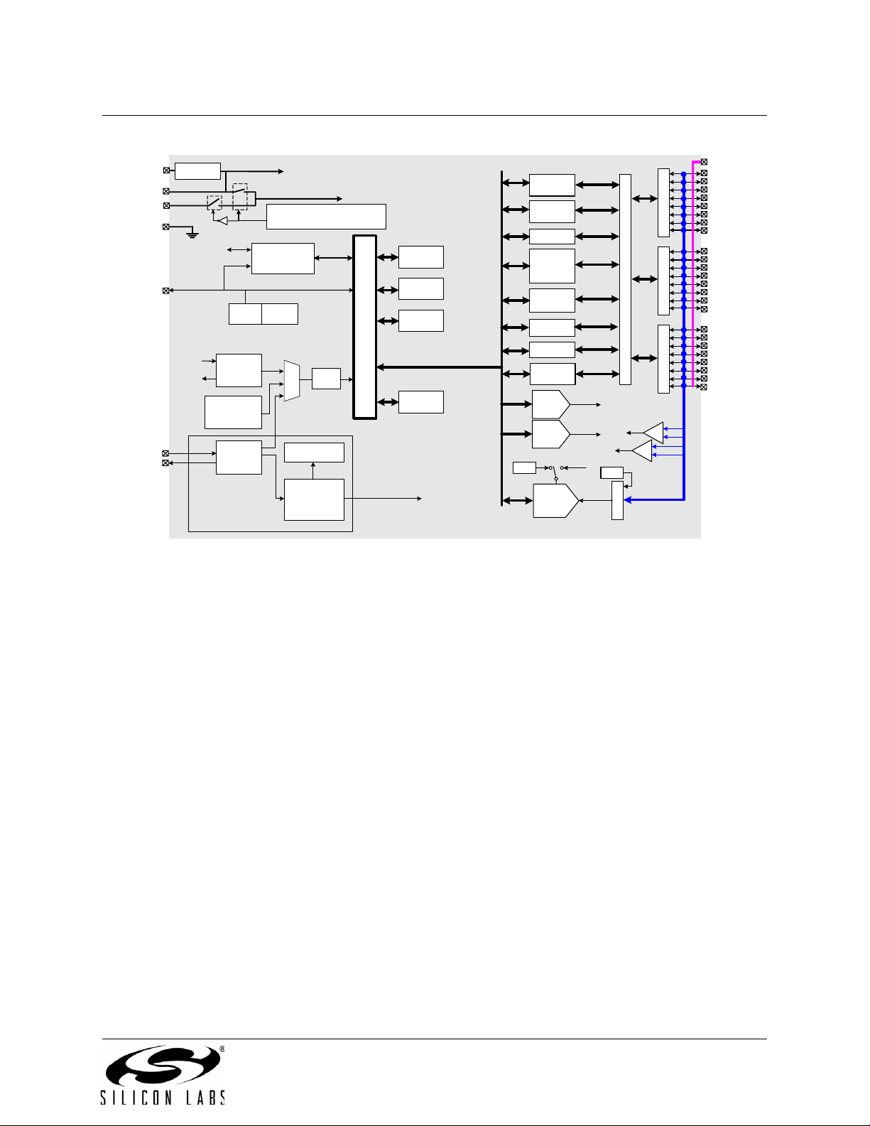
1. System Overview
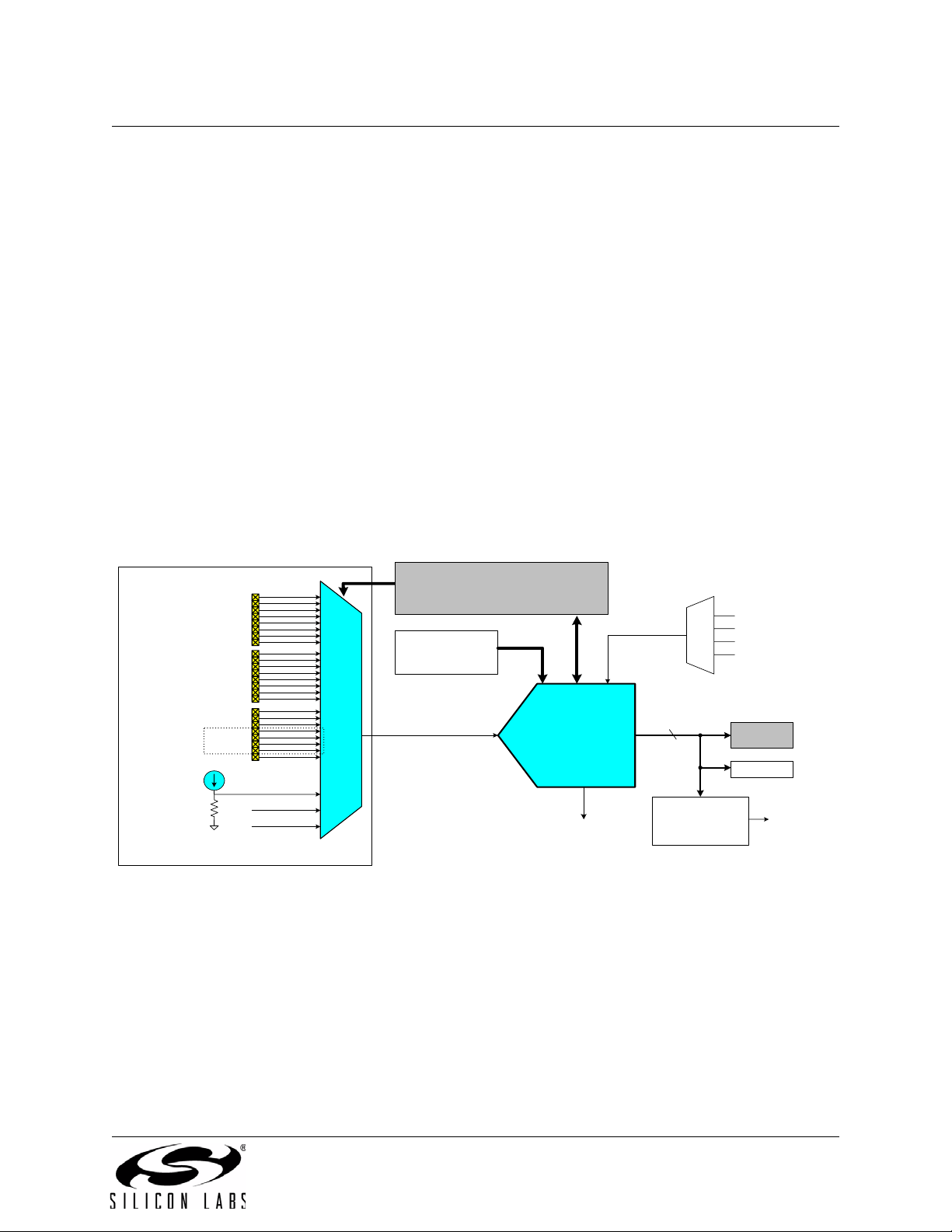
C8051F41x devices are fully integrated, low power, mixed-signal system-on-a-chip MCUs. Highlighted features are listed below. Refer to Table 1.1 for specific product feature selection.
• High-speed pipelined 8051-compatible microcontroller core (up to 50 MIPS)
• In-system, full-speed, non-intrusive debug interface (on-chip)
• True 12-bit 200 ksps ADC with analog multiplexer and 24 analog inputs
• Two 12-bit Current Output DACs
• Precision programmable 24.5 MHz internal oscillator
• Up to 32 kB bytes of on-chip Flash memory
• 2304 bytes of on-chip RAM
• SMBus/I2C, Enhanced UART, and SPI serial interfaces implemented in hardware
• Four general-purpose 16-bit timers
• Programmable Counter/Timer Array (PCA) with six capture/compare modules and Watchdog Timer
function
• Hardware smaRTClock (Real Time Clock) operates down to 1 V with 64 bytes of Backup RAM and a
Backup Voltage Regulator
• Hardware CRC Engine
• On-chip Power-On Reset, VDD Monitor, and Temperature Sensor
• On-chip Voltage Comparators
• Up to 24 Port I/O
With on-chip Power-On Reset, VDD monitor, Watchdog Timer, and clock oscillator , the C8051F41x devices
are truly standalone system-on-a-chip solutions. Th e Fl as h m emo ry c an be re progr am med ev en in -c irc ui t,
providing non-volati le data storage , and also allow ing field upg rades of the 8051 firmware. U ser software
has complete contr ol of all peripherals, a nd may individually shut down any or all peripher als for power
savings.
The on-chip Silicon Laboratories 2-Wire (C2) Development Interface allows non-intrusive (uses no on-chip
resources), full speed, in-circuit debugging using the production MCU installed in the final application. This
debug logic supports inspection and modification of memory and registers, setting breakpoints, single
stepping, run and halt commands. All a nalog and digital peripheral s are fully function al while debugging
using C2. The two C2 i nterface pins can be shared with us er functions, allowi ng in-system pro gramming
and debugging without occupying package pins.
Each device is specified for 2.0-to-2.75 V operation (supply voltage can be up to 5.25 V using on-chip regulator) over the industrial temperature range (–45 to +85 °C). The C8051F41x are available in 28-pin QFN
(also referred to as MLP or MLF) or 32-pin LQFP packages.
Rev. 1.0 19
Page 20
C8051F410/1/2/3
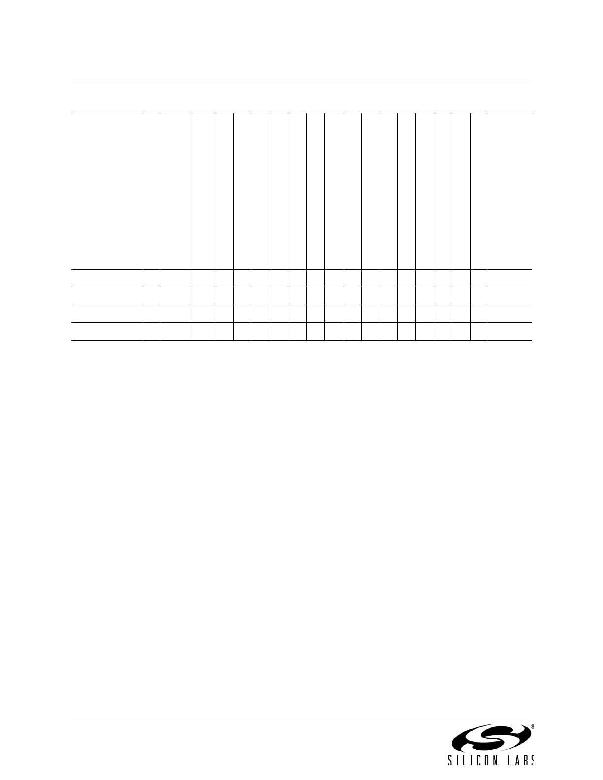
Table 1.1. Product Selection Guide
Ordering Part Number
C8051F410-GQ 50 32 kB 2368
C8051F411-GM 50 32 kB 2368
C8051F412-GQ 50 16 kB 2368
C8051F413-GM 50 16 kB 2368
MIPS (Peak)
Flash Memory
RAM
Calibrated Internal 24.5 MHz Oscillator
Clock Multiplier
SMBus/I2C
SPI
3 3 3 3 3
3 3 3 3 3
3 3 3 3 3
3 3 3 3 3
UART
Timers (16-bit)
Programmable Counter Array
Port I/Os
12-bit ADC ±1 LSB INL
smaRTClock (Real Time Clock)
Two 12-bit Current Output DACs
Internal Voltage Reference
Temperature Sensor
Analog Comparators
Lead-Free (RoHS compliant)
4
3
24
3 3 3 3 3 3 3
4
3
20
3 3 3 3 3 3 3
4
3
24
3 3 3 3 3 3 3
4
3
20
3 3 3 3 3 3 3
Package
LQFP-32
QFN-28
LQFP-32
QFN-28
20 Rev. 1.0
Page 21
C8051F410/1/2/3
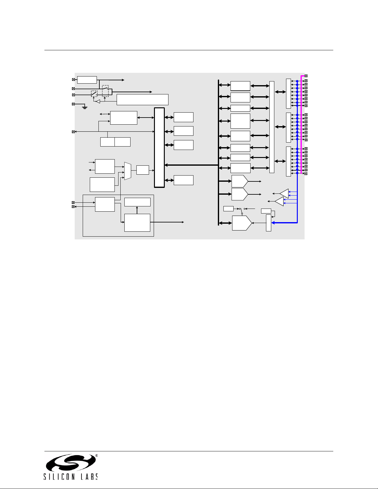
VREGIN
VDD
VRTC-BACKUP
GND
/RST/C2CK
XTAL3
XTAL4
VREG
C2D
XTAL1
XTAL2
24.5 MHz
2% Oscillator
smaRTClock Block
(to rest of chip)
POR
External
Oscillator
Circuit
32 KHz
Oscillator
(to smarRTClock Block)
Battery Switch-Over Circuit
(VDD >= VRTC-BACKUP)
Debug HW
Reset
Brown-
Out
Clock
Mult.
64B RAM
smaRTClock
State
Machine
x16
8
FLASH
0
5
1
C
SFR Bus
o
r
e
smaRTClock Alarm
Engine
32 kB
256 B
SRAM
2 kB
XRAM
CRC
VREF
Port 0
Latch
Port 1
Latch
UART
Timer
0,1,2,3
PCA x6 /
WDT
SMBus
SPI
Port 2
Latch
12-bit
IDAC0
12-bit
IDAC1
12-bit
200 ksps
ADC
VDD
IDAC0
IDAC1
Temp
VIO
P
0
D
r
v
C
R
P
O
1
S
S
D
B
r
A
v
R
P
2
D
r
v
CP0
+
-
CP1
+
-
A
AIN0-AIN23
M
U
X
P0.0/IDAC0
P0.1/IDAC1
P0.2
P0.3
P0.4/TX
P0.5/RX
P0.6/CNVST
P0.7
P1.0/XTAL1
P1.1/XTAL2
P1.2/VREF
P1.3
P1.4
P1.5
P1.6
P1.7
P2.0
P2.1
P2.2
P2.3
P2.4
P2.5
P2.6
P2.7/C2D
Figure 1.1. C8051F410 Block Diagram
Rev. 1.0 21
Page 22
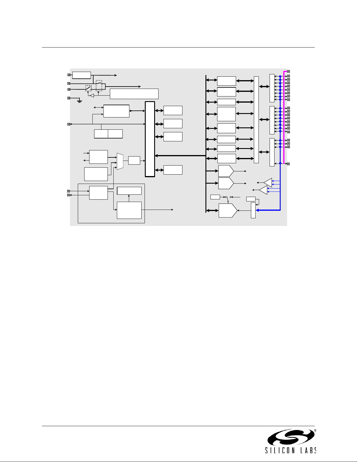
C8051F410/1/2/3
VREGIN
VDD
VRTC-BACKUP
GND
/RST/C2CK
XTAL3
XTAL4
VREG
C2D
XTAL1
XTAL2
24.5 MHz
2% Oscillator
smaRTClock Block
(to rest of chip)
POR
External
Oscillator
Circuit
32 KHz
Oscillator
(to smaRTClock Block)
Battery Sw itch - O ve r C irc ui t
(VDD >= VRTC -BACKUP)
Debug HW
Reset
Brown-
Out
Clock
Mult.
64B RAM
smaRTClock
State
Machine
x16
8
FLASH
0
5
1
C
SFR Bus
o
r
e
smaRTClock Alarm
Engine
32 kB
256 B
SRAM
2 kB
XRAM
CRC
VREF
Port 0
Latch
Port 1
Latch
UART
Timer
0,1,2,3
PCA x6 /
WDT
SMBus
SPI
Port 2
Latch
12-bit
IDAC0
12-bit
IDAC1
12-bit
200 ksps
ADC
VDD
IDAC0
IDAC1
Temp
VIO
P
0
D
r
v
C
R
P
O
1
S
S
D
B
r
A
v
R
P
2
D
r
v
CP0
+
-
CP1
+
-
A
AIN0-AIN20
M
U
X
P0.0/IDAC0
P0.1/IDAC1
P0.2
P0.3
P0.4/TX
P0.5/RX
P0.6/CNVST
P0.7
P1.0/XTAL1
P1.1/XTAL2
P1.2/VREF
P1.3
P1.4
P1.5
P1.6
P1.7
P2.0
P2.1
P2.2
P2.7/C2D
Figure 1.2. C8051F411 Block Diagram
22 Rev. 1.0
Page 23
C8051F410/1/2/3
VREGIN
VDD
VRTC-BACKUP
GND
/RST/C2CK
XTAL3
XTAL4
VREG
C2D
XTAL1
XTAL2
24.5 MHz
2% Oscilla to r
smaRTClock Block
(to rest of chip)
POR
External
Oscillator
Circuit
32 KHz
Oscillator
(to smaRTClocl Block)
Battery Switch-Over Circuit
(VDD >= VRTC-BACKUP)
Debug HW
Reset
Brown-
Out
Clock
Mult.
64B RAM
smaRTClock
State
Machine
x16
8
FLASH
0
5
1
C
SFR Bus
o
r
e
smaRTClock Alarm
Engine
16 kB
256 B
SRAM
2 kB
XRAM
CRC
VREF
Port 0
Latch
Port 1
Latch
UART
Timer
0,1,2,3
PCA x6 /
WDT
SMBus
SPI
Port 2
Latch
12-bit
IDAC0
12-bit
IDAC1
12-bit
200 ksps
ADC
VDD
IDAC0
IDAC1
Temp
VIO
P
0
D
r
v
C
R
P
O
1
S
S
D
B
r
A
v
R
P
2
D
r
v
CP0
+
-
CP1
+
-
A
AIN0-AIN23
M
U
X
P0.0/IDAC0
P0.1/IDAC1
P0.2
P0.3
P0.4/TX
P0.5/RX
P0.6/CNVST
P0.7
P1.0/XTAL1
P1.1/XTAL2
P1.2/VREF
P1.3
P1.4
P1.5
P1.6
P1.7
P2.0
P2.1
P2.2
P2.3
P2.4
P2.5
P2.6
P2.7/C2D
Figure 1.3. C8051F412 Block Diagram
Rev. 1.0 23
Page 24
C8051F410/1/2/3
VREGIN
VDD
VRTC-BACKUP
GND
/RST/C2CK
XTAL3
XTAL4
VREG
C2D
XTAL1
XTAL2
24.5 MHz
2% Oscillato r
smaRTClock Block
(to rest of chip)
POR
External
Oscillator
Circuit
32 KHz
Oscillator
(to smaRTClock Block)
Battery Switch-Over Circuit
(VDD >= VRTC-BACKUP)
Debug HW
Reset
Brown-
Out
Clock
Mult.
64B RAM
smaRTClock
State
Machine
x16
8
FLASH
0
5
1
C
SFR Bus
o
r
e
smaRTClock Alarm
Engine
16 kB
256 B
SRAM
2 kB
XRAM
CRC
VREF
Port 0
Latch
Port 1
Latch
UART
Timer
0,1,2,3
PCA x6 /
WDT
SMBus
SPI
Port 2
Latch
12-bit
IDAC0
12-bit
IDAC1
12-bit
200 ksps
ADC
VDD
IDAC0
IDAC1
Temp
VIO
P
0
D
r
v
C
R
P
O
1
S
S
D
B
r
A
v
R
P
2
D
r
v
CP0
+
-
CP1
+
-
A
AIN0-AIN20
M
U
X
P0.0/IDAC0
P0.1/IDAC1
P0.2
P0.3
P0.4/TX
P0.5/RX
P0.6/CNVST
P0.7
P1.0/XTAL1
P1.1/XTAL2
P1.2/VREF
P1.3
P1.4
P1.5
P1.6
P1.7
P2.0
P2.1
P2.2
P2.7/C2D
Figure 1.4. C8051F413 Block Diagram
24 Rev. 1.0
Page 25

C8051F410/1/2/3
1.1. CIP-51™ Microcontroller
1.1.1. Fully 8051 Compatible Instruction Set
The C8051F41x devices use Silicon Laboratories’ proprietary CIP-51 microcontroller core. The CIP-51 is
fully compatible with the MCS-5 1™ instruc tion se t. Standard 803x/805x assembl ers and compile rs can be
used to develop software. The C8051F41x family has a superset of all the peripherals included with a stan
dard 8052.
1.1.2. Improved Throughput
The CIP-51 employs a pipelined architecture that greatly increases its instruction throughput over the standard 8051 architecture. In a standard 8051, all ins truction s except for MU L and DIV take 12 or 24 syste m
clock cycles to execute, and usually have a maximum system clock of 12-to-24
51 core executes 70% of its instructions in one or two system clock cycles, with no instructions taking more
than eight system clock cycles.
With the CIP-51's system clock running at 50 MHz, it has a peak throughput of 50 MIPS. The CIP-51 has a
total of 109 instructions. The table below shows the total number of instructions that require each execution
time.
MHz. By contrast, the CIP-
-
Clocks to Execute 1 2 2/4 3 3/5 4 5 4/6 6 8
Number of Instructions 26 50 5 10 7 5 2 1 2 1
1.1.3. Additional Features
The C8051F41x SoC famil y includes several key enhancements to the CIP-51 co re and peripherals to
improve performance and ease of use in end applications.
An extended interrupt handler allows the numerous analog and digital peripherals to operate independently of the controller core and interrupt the controller only when necessary. By requiring less intervention
from the microcontrol ler co re, an interru pt-driv en sy stem is more efficient and a llows for eas ier impl emen
tation of multi-tasking, real-time systems.
Eight reset sources are available: power-on reset ci rcuitry (POR), an on-chip VDD monitor, a Watchdog
Timer, a Missing Clock Detector, a voltage level detection from Comparator0, a smaRTClock alarm or
missing smaRTClock cl ock detector reset, a forced software reset, an ex ternal reset pin, and an illegal
Flash access protection circuit. Each reset source except for the POR, Reset Input Pin, or Flash error may
be disabled by the user in so ftware. The WDT may be permanently enab led in software after a pow er-on
reset during MCU initialization.
The internal oscillator is factory calibrated to 24.5 MHz ±2%. An external oscillator drive circuit is also
included, allowing an external crystal, ceramic resonator, capacitor , RC, or CMOS clock source to generate
the system clock. A clock multiplier allows for operation at up to 50
lator can be extremel y useful in low power applications, allowi ng the system to maintain accurate time
while the MCU is not po wered, or its internal oscillator is sus pended. The MCU ca n be reset or have its
oscillator awakened using the smaRTClock alarm function.
MHz. The dedicated smaRTClock oscil-
-
Rev. 1.0 25
Page 26
C8051F410/1/2/3
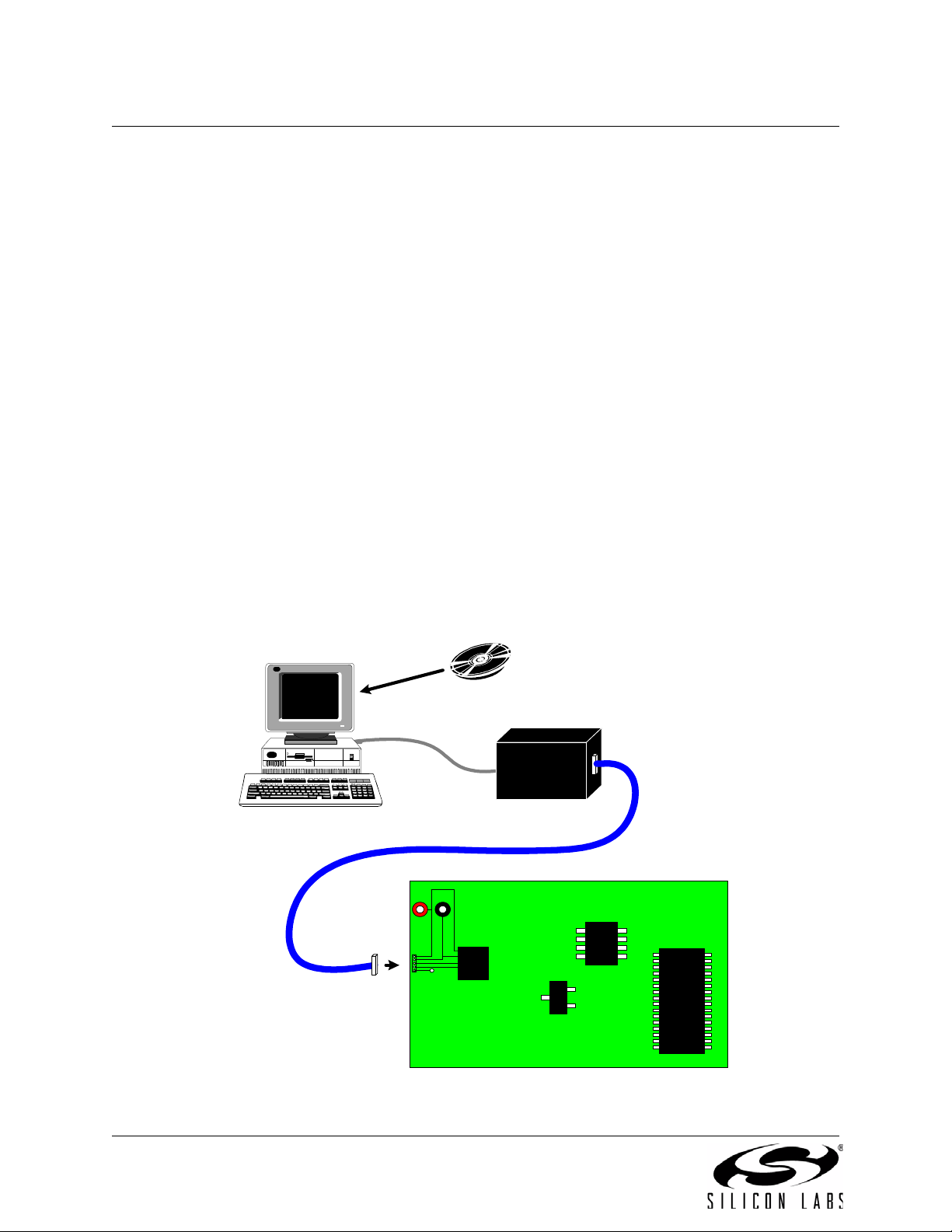
1.2. On-Chip Debug Circuitry
The C8051F41x devices include on-chip Silicon La boratories 2-Wire (C2) debug circuitry that provides
non-intrusive, full speed, in-circuit debugging of the production part installed in the end application.
Silicon Laboratories’ debugging system supports inspection and modification of memory and registers,
breakpoints, and single stepping . No addi tional targe t RAM, prog ram memo ry, timers, or communications
channels are required. All the digital and analog peripherals are functional and work correctly while debug
ging. All the peripherals (except for the ADC and SMBus) are stalled when the MCU is halted, during single
stepping, or at a breakpoint in order to keep them synchronized.
The C8051F410DK development kit provides all the hardware and software necessary to develop application code and perfo rm in-circuit debugging wi th the C8051F41x MCUs. The k it includes software with a
developer's studio and debugger, a USB debug adapter, a target applicati on board with the associated
MCU installed, and the required cables and wall-mount power supply. The development kit requires a com
puter with Windows®98 SE or later installed . As shown in Figure 1.5, the PC is connected to the USB
debug adapter. A six-inch ribbon cable connects th e USB debug ad apter to the user's application boa rd,
picking up the two C2 pins and GND.
The Silicon Labor atories ID E interface is a vastly superior deve loping a nd debugging configuration, compared to standard MCU em ulators that use on-b oard "ICE Chi ps" and requi re the MCU in the app lication
board to be socketed. Sil icon La bor ato rie s’ de bug paradi gm i ncre ases ease of use and preserves the per
formance of the precision analog peripherals.
-
-
-
WINDOWS 98 SE or later
Silicon Laboratories Integrated
Development Environment
USB
Debug
Adapter
C2 (x2), GND
VDD GND
C8051F41x
TARGET PCB
Figure 1.5. Development/In-System Debug Diagram
26 Rev. 1.0
Page 27
C8051F410/1/2/3
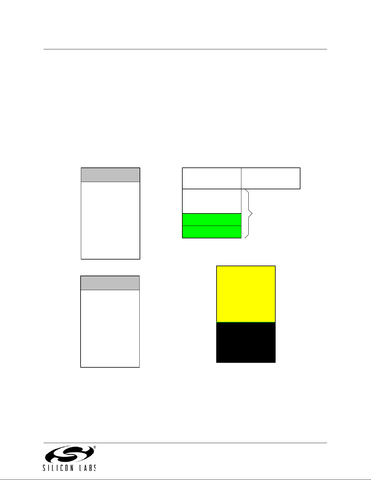
1.3. On-Chip Memory
The CIP-51 has a standa rd 8051 program and data addr ess configuration. It inc ludes 256 bytes of data
RAM, with the upper 128 bytes dual-mapped. Indirect addressing accesses the upper 128 bytes of general
purpose RAM, and d irect addr essing a ccesses the 128-by te SFR add ress space. The lower 128 bytes of
RAM are accessible via direct and indirect addressing. The first 32 bytes are addressable as four banks of
general purpose registers, and the next 16 bytes can be byte addressable or bit addressable.
Program memory con sists of 32 kB (‘F410/1) or 16 kB (‘F41 2/3) of Flash. This memory may be reprogrammed in-system in 512 byte sectors and requires no special off-chip programming voltage.
PROGRAM/DATA MEMORY
(Flash)
‘F410/1
0x7E00
0x7DFF
0x0000
0x4000
0x3FFF
RESERVED
32 kB Flash
(In-System
Programmab le in 51 2
Byte Sectors)
‘F412/3
RESERVED
16 kB Flash
(In-System
Programmable in 512
Byte Sectors)
0xFF
0x80
0x7F
0x30
0x2F
0x20
0x1F
0x00
DATA MEMORY (RAM)
INTERNAL DATA ADDRESS SPACE
Upper 128 RAM
(Indirect Addressing
Only)
(Direct and Indirect
Addressing)
Bit Addressable
General Purpose
Registers
Special Function
Register's
(Direct Addressing Only)
Lower 128 RAM
(Direct and Indirect
Addressing)
EXTERNAL DATA ADDRESS SPACE
0xFFFF
Same 2048 bytes as from
0x0000 to 0x07FF, wrapped
on 2048-byte boundaries
0x0800
0x07FF
XRAM - 2048 Bytes
(accessible using MOVX
instruction)
0x0000
0x0000
Figure 1.6. Memory Map
Rev. 1.0 27
Page 28

C8051F410/1/2/3
1.4. Operating Modes
The C8051F41x devices have four operating modes: Active (Normal), Idle, Suspend, and Stop. Active
mode occurs during normal ope ration when the oscillator and peri pherals are active. Idle mode halts the
CPU while leaving the peripherals and internal clocks active. Suspend mode halts SYSCLK until a waken
ing event occurs, which also halts all peripherals using SYSCLK. In Stop mode, the CPU is halted, all interrupts and timers are inactive, and the internal oscillator is stopped. The various operating modes are
described in
Table 1.2 below:
Table 1.2. Operating Modes Summary
-
Active
Idle
Suspend
Stop
Properties
•SYSCLK active
• CPU active (accessing Flash)
• Peripherals active or inactive
depending on user settings
• smaRTClock active or inactive
•SYSCLK active
• CPU inactive (not accessing
Flash)
• Peripherals active or inactive
depending on user settings
• smaRTClock active or inactive
•SYSCLK inactive
• CPU inactive (not accessing
Flash)
• Peripherals enabled (but not
operating) or disabled depend
ing on user settings
• smaRTClock active or inactive
•SYSCLK inactive
• CPU inactive (not accessing
Flash)
• Digital peripherals inactive;
analog peripherals enabled
(but not operating) or disabled
depending on user settings
• smaRTClock inactive
Power
Consumption
Full — —
Less than Full IDLE
Low SUSPEND
-
Very low STOP
How
Entered?
(PCON.0)
(OSCICN.5)
(PCON.1)
How Exited?
Any enabled
interrupt or
device reset
Wakening
event or exter
nal/MCD reset
External or
MCD reset
-
See Section “10.3. Power Management Modes” on page 101 for Idle and Stop mode details. See Sec-
tion “19.1.1. Internal Oscillator Suspend Mode” on page 166 for more information on Suspend mode.
28 Rev. 1.0
Page 29
C8051F410/1/2/3
1.5. 12-Bit Analog to Digital Converter
The C8051F41x devices include an on-ch ip 12-bit SAR ADC wit h a 27-channel single -ended input mul tiplexer and a maximum throughput of 200 ksps. The ADC system includes a configurable analog m ultiplexer that selects the positive ADC input, which is measured with respect to GND. Ports 0–2 are available
as ADC inputs; additionally, the on-chip Temperature Sensor output and the co re sup ply vo ltage (V
available as ADC inputs. User firmware may shut down the ADC or use it in Burst Mode to save power.
Conversions can be started in four wa ys: a s oftware comman d, an ove rf low of Timer 2 or 3, or an ex ternal
convert start signal. This flexibility allows the start of conversion to be triggered by software events, a peri
odic signal (timer ov erfl ows ), or ex ternal HW si gn als . Co nv ersi on c om pl eti ons ar e i ndicated by a status bit
and an interrupt (if enab led ) and occ ur a fter 1, 4 , 8, o r 1 6 s amp le s h av e be en ac cumulated by a hardware
accumulator. The resulting data word is latched into the ADC data SFRs upon completion of a conversion.
When the system clo ck is slow, Burst Mode allows ADC0 to automa tically wake from a low pow er shut
down state, acquire and accu mulate samples, then re-enter the low power shutdown state without CPU
intervention.
Window compare registers for the ADC data can be configured to interrupt the controller when ADC data is
either within or o utside of a specified range. Th e ADC can monitor a key v oltage continuously in back
ground mode, but not interrupt the controller unless the converted data is within/outside the specified
range.
DD
) are
-
-
-
P2.3-2.6
available on
C8051F410/2
Temp
Sensor
Analog Multiplexer
P0.0
P0.7
P1.0
P1.7
P2.0
P2.7
VDD
GND
19-to-1
AMUX
Configuration, Control, and Data Registers
Burst Mode
Logic
12-Bit
SAR
ADC
End of
Conversion
Interrupt
Start
Conversion
16
Window Compare
Logic
AD0BUSY (W)
Timer 3 Overflow
CNVSTR Rising Edge
Timer 2 Overflow
ADC Data
Registers
Accumulator
Window
Compare
Interrupt
Figure 1.7. 12-Bit ADC Block Diagram
1.6. Two 12-bit Current-Mode DA Cs
The C8051F41x devices in cl ude two 12-bit current-mode Digital-to-Analog Con verte rs (ID ACs ). Th e max imum current output of the IDACs can be adjusted for four different current settings; 0 .25 mA, 0.5 mA,
1
mA, and 2 mA. A flexible output update mechanism allows for seamless full-scale changes, and supports
jitter-free updates for waveform generation. The IDAC outputs can be merged onto a single port I/O pin for
increased full -scale current ou tput or increase d resolution. IDAC updates can be p erformed on-dem and,
scheduled on a Timer overflow, or synchronized with an external signal.
of the IDAC circuitry.
Figure 1.8 shows a block diagram
Rev. 1.0 29
Page 30
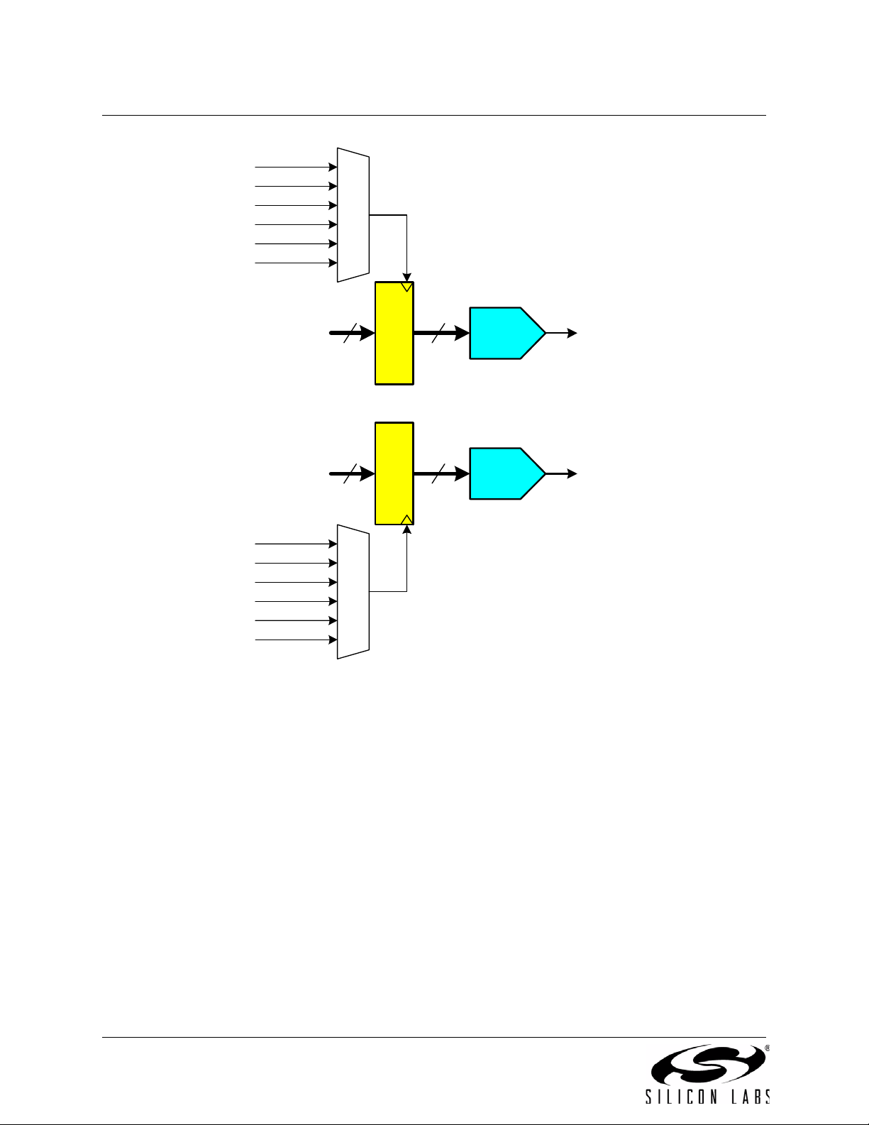
C8051F410/1/2/3
nt
t
1
nt
t
1
Data Write
Timer 0
Timer 1
Timer 2
Timer 3
CNVSTR
2-bit Digital
12
Input
2-bit Digital
12
Input
Data Write
Timer 0
Timer 1
Timer 2
Timer 3
CNVSTR
Figure 1.8. IDAC Block Diagram
1.7. Programmable Compa rat ors
12
IDA0
Latch
12
IDA1
Latch
Curre
Outpu
Curre
Outpu
C8051F41x devices include two software-configurable voltage comparators with an input multiplexer. Each
comparator offers programmable response time and hyst eresis and two outputs that are opti onally avail
able at the Port pins: a synchrono us “latched” output (CP0 and CP1), or an asynch ronous “raw” output
(CP0A and CP1A). Co mparator interrupts may be generated on rising, falling, or both edges. When in
IDLE or SUSPEND mode, these interrupts may be used as a “wake-up” source for the processor.
Comparator0 may also be conf igured as a reset source. A block diagram of the comparato r is shown in
Figure 1.9.
-
30 Rev. 1.0
Page 31

VDD
)
t)
)
t)
C8051F410/1/2/3
Inter rupt
Logic
Port I/O
Pins
Port I/O
Pins
Multiplexer
Multiplexer
+
-
+
-
GND
VDD
GND
Reset
Decision
Tree
SET
D
Q
CLR
Q
(SYNCHRONIZER)
SET
D
CLR
Inter rupt
SET
D
Q
CLR
Q
(SYNCHRONIZER)
SET
D
CLR
Q
Q
Logic
Q
Q
CP0
(synchronous output
CP0A
(asynchronous outpu
CP1
(synchronous output
CP1A
(asynchronous outpu
Figure 1.9. Comparator s Block Diagram
1.8. Cyclic Redundancy Check Unit
C8051F41x devices include a cyclic redundancy check unit (CRC0) that can perform a CRC using a 16-bit
or 32-bit polynomial . CRC0 accepts a stream of 8-bit data and out puts a 16-bi t o r 32-bi t r esul t. CRC 0 al s o
has a hardware bit reverse feature for quick data manipulation.
1.9. Voltage Regulator
C8051F41x devices incl ude an on-chip low dropout voltage regul ator (REG0). The input to REG0 at the
V
enabled, the output of REG0 powers the device and drives the V
to power external devices connected to V
pin can be as high as 5.25 V. The output can be selecte d by software to 2.0 V or 2.5 V. W h e n
REGIN
pin. The vol t ag e r egu la t or c an be used
DD
.
DD
1.10. Serial Ports
The C8051F41x Family includ es an SMBus/I2C interface, a full-duplex UA RT with enhanced baud rate
configuration, an d an Enhanced S PI interface. Eac h of the seri al buses is full y implemented in hardware
and makes extensive use of the CIP-51's interrupts, thus requiring very little CPU intervention.
Rev. 1.0 31
Page 32

C8051F410/1/2/3
1.11. smaRTClock (Real Time Clock)
C8051F41x device s include a smaRTClock Peripher al (Real Time Clock). The smaRTClock has a ded icated 32 kHz o scilla tor th at c an be co nfi gured for u se wi th o r with out a crystal, a 47-bit smaRTClock ti mer
with alarm, a backup supply regulator, and 64
(V
RTC-BACKUP
age (VDD) is lost.
The smaRTClock allows a maximum of 137 year 47-bit independent time-keeping when used with a
32.768
Clock from the backup s upply when the voltage at V
alarm and missing cloc k detector can interrupt the CIP-51, wake the internal oscillator from SUSPEND
mode, or generate a device reset if the smaRTClock timer reaches a pre-set value or the oscillator stops.
kHz Watch Crystal and backup supply voltage of at least 1 V. The switchover logic powers smaRT-
) is powered, the smaRTClock peripheral remains fully functional even if the core supply volt-
bytes of backup SRA M. When the backup su pply voltage
RTC-BACKUP
is greater than VDD. The smaRTClock
XTAL4
smaRTCloc k Os cillator
smaRTClock State Machine
64B
Backup RAM
Backup
Regulator
Switchover
Logic
XTAL3
Interrupt
Internal
Registers
CAPTUREn
RTC0CN
RTC0XCN
ALARMn
RAMADDR
RAMDATA
smaRTClock
47-Bit
smaRTClock
Timer
Interface
Registers
RTC0KEY
RTC0ADR
RTC0DAT
CIP-51 CPU
V
DD
V
RTC-BACKUP
Figure 1.10. smaRTClock Block Diagram
32 Rev. 1.0
Page 33

C8051F410/1/2/3
1.12. Port Input/Output
C8051F41x devices include up to 24 I/O pins. Port pins a re organized as three byte-w ide ports. The p ort
pins behave like ty pi ca l 805 1 p or ts wi th a fe w e nha nc eme nts. E ac h p ort p in can be c onfi gur ed a s a dig ital
or analog I/O pin. Pins se lec te d as dig ital I/O c an be con figured for push-pull or open-dr ai n op erati on. The
“weak pullups” that are fixed on typical 8051 devices may be individually or globally disabled to save
power.
The Digital Crossbar allows mapping of internal digital system resources to port I/O pins. On-chip
counter/timers, ser ial bu ses, hardware i nte rrupts, and oth er dig ital signals can be c onfigu red to a ppear on
the port pins using the Cr ossbar cont rol regis ters. This a llows the us er to select the exact m ix of genera lpurpose port I/O, digital, and analog resources needed for the application.
Highest
Priority
Lowest
Priority
XBR0, XBR1,
PnSKIP Registers
Priority
Decoder
UART
SPI
SMBus
2
4
2
Digital
Crossbar
CP0
CP1
Outputs
SYSCLK
(Internal Digital Signals)
PCA
T0, T1
P0
(P0.0-P0.7)
P1
(P1.0-P1.7)
4
7
2
8
8
P0MASK, P0MATCH
P1MASK, P1MATCH
Registers
PnMDIN Registers
8
8
8
P0
I/O
Cells
P1
I/O
Cells
P2
I/O
Cell
P2.3–2.6 available on
C8051F410/2
PnMDOUT,
P0.0
P0.7
P1.0
P1.7
P2.0
P2.7
(Port Latches)
P2
(P2.0-P2.7)
8
Figure 1.11. Port I/O Functional Block Diagram
Rev. 1.0 33
Page 34

C8051F410/1/2/3
1.13. Programmable Counter Array
The Programmable Count er Arr ay (PCA0 ) provi des en hance d timer functiona lity while req uiri ng less CP U
intervention than the standard 80 51 counter/tim ers. The PCA con sists of a dedicated 16 -bit counter/timer
and six 16-bit capture/co mpare modules. The counter/timer is driven by a programmable timebase that
can select betwee n seven sources: syst em clock, system clock di vided by four, system clock divided by
twelve, the external os cil la tor cl ock source divided by 8, real- tim e c loc k source divided by 8, Timer 0 over
flow, or an external clock signal on the External Clock Input (ECI) pin.
Each capture/com pare module may be configured to operate independently in o ne of six modes: EdgeTriggered Capture, Software Timer, High-Speed Output, Frequency Output, 8-Bit P WM, or 16-Bit PWM.
Additionally, PCA Module 5 may be u sed as a watchd og t imer (WDT ), an d is enab le d in this mode fo llow
ing a system reset. The PCA Cap tur e/Co mpare Modu le I/O and the Ex terna l Clo ck Input may be routed to
Port I/O using the digital crossbar.
SYSCLK/12
SYSCLK/4
Timer 0 Overflow
ECI
SYSCLK
External Clock/8
smaRTClock/8
PCA
CLOCK
MUX
16-Bit Counter/Timer
-
-
Capture/Compare
Module 0
ECI
CEX0
Capture/Compare
Module 1
CEX1
Capture/Compare
Module 2
CEX2
Capture/Compare
Module 3
CEX3
Capture/Compare
Module 4
CEX4
Capture/Compare
Module 5
CEX5
Crossbar
Port I/O
Figure 1.12. PCA Block Diagram
34 Rev. 1.0
Page 35

C8051F410/1/2/3
2. Absolute Maximum Ratings
Table 2.1. Absolute Maximum Ratings*
Parameter Conditions Min Typ Max Units
Ambient temperature under bias –55 — 125 °C
Storage Temperature –65 — 150 °C
Voltage on V
Voltage on V
Voltage on V
Voltage on XTAL1 with respect to GND –0.3 — V
Voltage on XTAL3 with respect to GND –0.3 — 5.5 V
with respect to GND –0.3 — 5.5 V
REGIN
with respect to GND –0.3 — 3.0 V
DD
RTC-BACKUP
with respect to GND –0.3 — 5.5 V
+ 0.3 V
DD
Voltage on any Port I/O Pin (except Port 0 pins) or
RST
with respect to GND
–0.3 — V
+ 0.3 V
IO
Voltage on any Port 0 Pin with respect to GND 0.3 — 5.5 V
Maximum output current sunk by any Port pin — — 100 mA
Maximum output current sourced by any Port pin — — 100 mA
Maximum Total current through V
V
RTC-BACKUP
*Note: S tre sses abov e those lis ted under “Abs olute Maxim um Ratin gs” may cau se permanent d amage to the device.
, V
This is a stress rating only and f unctional operation of the devi ces at th ose or any other cond itions ab ove those
indicated in the o peration l istings of this spe cificati on is not implied. Exposur e to maxim um rating conditio ns for
extended periods may affect device reliability.
REGIN
, and GND
DD
, VIO,
——500mA
Rev. 1.0 35
Page 36

C8051F410/1/2/3
3. Global DC Electrical Characteristics
Table 3.1. Global DC Electrical Characteristics
–40 to +85 °C, 50 MHz System Clock unless otherwise specified. Typical values are given at 25 °C
Parameter Conditions Min Typ Max Units
Supply Input Voltage (V
REGIN
1
)
Core Supply Voltage (VDD) 2.0 — 2.75 V
I/O Supply Voltage (VIO) 2.0 — 5.25 V
Output Current = 1 mA 2.15 — 5.25 V
Backup Supply Voltage (V
RTC-BACKUP
Backup Supply Current
(I
RTC-BACKUP
(V
= 0 V, smaRTClock clock = 32 kHz)
DD
)
2
)
V
RTC-BACKUP
= 1.0 V:
at –40 ºC
at 25 ºC
at 85 ºC
V
RTC-BACKUP
= 1.8 V:
at –40 ºC
at 25 ºC
at 85 ºC
V
RTC-BACKUP
= 2.5 V:
at –40 ºC
at 25 ºC
at 85 ºC
1.0 — 5.25 V
—
—
—
—
—
—
—
—
—
0.65
0.9
1.4
0.7
0.92
1.45
0.72
0.95
1.5
1.5
1.8
2.5
—
—
—
1.6
1.85
2.6
µA
µA
µA
µA
µA
µA
µA
µA
µA
Core Supply RAM Data Retention Voltage — 1.5 — V
SYSCLK (System Clock)
3,4
0 — 50 MHz
Specified Operating Temperature Range –40 — +85 °C
Notes:
1. For more information on V
2. The Backup Supply Voltage (V
characteristics, see Table 8.1 on page 82.
REGIN
RTC-BACKUP
) is used to power the smaRTClock peripheral only.
3. SYSCLK is the internal device clock. For operational speeds in excess of 25 MHz, SYSCLK must
be derived from the internal clock multiplier.
4. SYSCLK must be at least 32 kHz to enable debugging.
5. Based on device character izati on data, not producti on tes ted.
6. Active and Inactive IDD at voltages and frequencies other than those specified can be calculated
using the IDD Supply Sensitivity. For example, if the V
I
= 5.5 mA typical at 2.0 V and f = 25 MHz. From this, IDD = 5.5 mA + 1.14 x (2.2 V –
DD
is 2.2 V instead of 2.0 V at 25 MHz:
DD
2.0 V) = 5.73 mA at 2.2 V and f = 25 MHz.
7. I
can be estimated for frequencies < 15 MHz by simply multiplying the frequency of interest by the
DD
frequency sensitivity number for that range. When using these numbers to estimate I
15
MHz, the estimate should be the current at 25 MHz minus the difference in current indicated by
the frequency sensitivity number. For example: V
= 2.0 V; F = 20 MHz, IDD = 5.5 mA – (25 MHz –
DD
DD
for >
20 MHz) x 0.16 mA/MHz = 4.7 mA.
8. Idle IDD can be estimated for frequencies < 1 MHz by simply multiplying the frequency of interest by
the frequency sensitivity number for that range. When using these numbers to estimate Idle for >
1
MHz, the estimate should be the current at 25 MHz minus the difference in current indica ted by
the frequency sensitivity number. For example: V
= 2.0 V; F = 5 MHz, Idle IDD = 2.8 mA –
DD
(25 MHz – 5 MHz) x 0.1 mA/MHz = 0.8 mA.
36 Rev. 1.0
Page 37

C8051F410/1/2/3
Table 3.1. Global DC Electrical Characteristics (Continued)
–40 to +85 °C, 50 MHz System Clock unless otherwise specified. Typical values are given at 25 °C
Parameter Conditions Min Typ Max Units
Digital Supply Current—CPU Active (Normal Mode, fetching instructions from Flash)
Core Supply Current (IDD)
5
VDD = 2.0 V:
F = 32 kHz
F = 1 MHz
F = 25 MHz
F = 50 MHz
—
—
—
—
13
0.30
5.5
9.5
30
0.5
6.5
12
VDD = 2.5 V:
Supply Sensitivity (IDD)
5,6
Frequency Sensitivity (IDD)
5,7
F = 32 kHz
F = 1 MHz
F = 25 MHz
F = 50 MHz
F = 25 MHz
F = 1 MHz
VDD = 2.0 V:
F < 15 MHz, T = 25 ºC
F > 15 MHz, T = 25 ºC
—
—
—
—
—
—
—
—
17
0.43
8.3
13.5
114
100
0.27
0.16
40
0.65
9.5
15
—
—
—
—
mA/MHz
mA/MHz
VDD = 2.5 V:
F < 15 MHz, T = 25 ºC
F > 15 MHz, T = 25 ºC
—
—
0.39
0.2
—
—
mA/MHz
mA/MHz
Notes:
1.
For more information on V
2. The Backup Supply Voltage (V
characteristics, see Table 8.1 on page 82.
REGIN
RTC-BACKUP
) is used to power the smaRTClock peripheral only.
3. SYSCLK is the internal device clock. For operational speeds in excess of 25 MHz, SYSCLK must
be derived from the internal clock multiplier.
4. SYSCLK must be at least 32 kHz to enable debugging.
5. Based on device character izati on data, not producti on tes ted.
6. Active and Inactive IDD at voltages and frequencies other than those specified can be calculated
using the IDD Supply Sensitivity. For example, if the V
I
= 5.5 mA typical at 2.0 V and f = 25 MHz. From this, IDD = 5.5 mA + 1.1 4 x (2.2 V –
DD
is 2.2 V instead of 2.0 V at 25 MHz:
DD
2.0 V) = 5.73 mA at 2.2 V and f = 25 MHz.
7. I
can be estimated for frequencies < 15 MHz by simply multiplying the frequency of interest by the
DD
frequency sensitivity number for that range. When using these numbers to estimate I
DD
for >
15 MHz, the estimate should be the current at 25 MHz minus the difference in current indicated by
the frequency sensitivity number. For example: V
= 2.0 V; F = 20 MHz, IDD = 5.5 mA – (25 MHz –
DD
20 MHz) x 0.16 mA/MHz = 4.7 mA.
8. Idle IDD can be estimated for frequencies < 1 MHz by simply multiplying the frequency of interest by
the frequency sensitivity number for that range. When using these numbers to estimate Idle for >
1 MHz, the estimate should be the current at 25 MHz minus the difference in current indicated by
the frequency sensitivity number. For example: V
= 2.0 V; F = 5 MHz, Idle IDD = 2.8 mA –
DD
(25 MHz – 5 MHz) x 0.1 mA/MHz = 0.8 mA.
µA
mA
mA
mA
µA
mA
mA
mA
%/V
%/V
Rev. 1.0 37
Page 38

C8051F410/1/2/3
Table 3.1. Global DC Electrical Characteristics (Continued)
–40 to +85 °C, 50 MHz System Clock unless otherwise specified. Typical values are given at 25 °C
Parameter Conditions Min Typ Max Units
Digital Supply Current—CPU Inactive (Idle Mode, not fetching instructions from Flash)
Core Supply Current (IDD)
5
VDD = 2.0 V:
F = 32 kHz
F = 1 MHz
F = 25 MHz
F = 50 MHz
VDD = 2.5 V:
F = 32 kHz
F = 1 MHz
F = 25 MHz
F = 50 MHz
Supply Sensitivity (IDD)
5,6
F = 25 MHz
F = 1 MHz
Frequency Sensitivity (IDD)
5,8
VDD = 2.0 V:
F < 1 MHz, T = 25 ºC
F > 1 MHz, T = 25 ºC
VDD = 2.5 V:
F < 1 MHz, T = 25 ºC
F > 1 MHz, T = 25 ºC
Digital Supply Current (Suspend Mode) Oscillator not running,
VDD = 2.5 V
Digital Supply Current
(Stop Mode, shutdown)
Oscillator not running,
VDD = 2.5 V
—
—
—
—
—
—
—
—
—
—
—
—
—
—
10
0.15
2.8
5
11
0.21
3.8
7.5
75
68
0.14
0.1
0.19
0.13
25
0.25
3.3
11
30
0.37
4.3
8.0
—
—
—
—
—
—
µA
mA
mA
mA
µA
mA
mA
mA
%/V
%/V
mA/MHz
mA/MHz
mA/MHz
mA/MHz
— 0.15 50 µA
— 0.15 50 µA
Notes:
1.
For more information on V
2. The Backup Supply Voltage (V
characteristics, see Table 8.1 on page 82.
REGIN
RTC-BACKUP
) is used to power the smaRTClock peripheral only.
3. SYSCLK is the internal device clock. For operational speeds in excess of 25 MHz, SYSCLK must
be derived from the internal clock multiplier.
4. SYSCLK must be at least 32 kHz to enable debugging.
5. Based on device character izati on data, not producti on tes ted.
6. Active and Inactive IDD at voltages and frequencies other than those specified can be calculated
using the IDD Supply Sensitivity. For example, if the V
I
= 5.5 mA typical at 2.0 V and f = 25 MHz. From this, IDD = 5.5 mA + 1.1 4 x (2.2 V –
DD
is 2.2 V instead of 2.0 V at 25 MHz:
DD
2.0 V) = 5.73 mA at 2.2 V and f = 25 MHz.
7. I
can be estimated for frequencies < 15 MHz by simply multiplying the frequency of interest by the
DD
frequency sensitivity number for that range. When using these numbers to estimate I
DD
for >
15 MHz, the estimate should be the current at 25 MHz minus the difference in current indicated by
the frequency sensitivity number. For example: V
= 2.0 V; F = 20 MHz, IDD = 5.5 mA – (25 MHz –
DD
20 MHz) x 0.16 mA/MHz = 4.7 mA.
8. Idle IDD can be estimated for frequencies < 1 MHz by simply multiplying the frequency of interest by
the frequency sensitivity number for that range. When using these numbers to estimate Idle for >
1 MHz, the estimate should be the current at 25 MHz minus the difference in current indicated by
the frequency sensitivity number. For example: V
= 2.0 V; F = 5 MHz, Idle IDD = 2.8 mA –
DD
(25 MHz – 5 MHz) x 0.1 mA/MHz = 0.8 mA.
38 Rev. 1.0
Page 39

C8051F410/1/2/3
Table 3.2. Index to Electrical Characteristics Tables
Table Title Page #
ADC0 Electrical Characteristics (VDD = 2.5 V, V
ADC0 Electrical Characteristics (VDD = 2.1 V, V
IDAC Electrical Characteristics 75
Voltage Reference Electrical Characteristics 79
Voltage Regulator Electrical Specifications 82
Comparator Electrical Characteristics 92
Reset Electrical Characteristics 134
Flash Electrical Characteri sti cs 143
Port I/O DC Electrical Characteristics 163
Oscillator Electrical Characteristics 175
= 2.2 V) 67
REF
= 1.5 V) 68
REF
Rev. 1.0 39
Page 40

C8051F410/1/2/3
NOTES:
40 Rev. 1.0
Page 41
4. Pinout and Package Definitions
Table 4.1. Pin Definitions for the C8051F41x
C8051F410/1/2/3
Name
V
DD
V
IO
GND
V
RTC-BACKUP
V
REGIN
RST/
C2CK
P2.7/
C2D
XTAL3 5 4 A In
Pin Numbers
‘F410/2 ‘F411/3
7 6
1 28
6 5
3 2
8 7
2 1
32 27
Type Description
Core Supply Voltage.
I/O Supply Voltage.
Ground.
smaRTClock Backup Sup pl y Voltage.
On-Chip Voltage Regulator Input.
D I/O
D I/O
D I/O
D I/O
Device Reset. Open-drain output of internal POR or VDD
monitor. An external source can initiate a system reset by
driving this pin low for at least 15
recommended. See Reset Sources Section for a complete
description.
Clock signal for the C2 Debug Interface.
Port 2.7. See Port I/O Section for a complete description.
Bi-directional data signal for the C2 Debug Interface.
smaRTClock Oscillator Crystal Input.
See Section 20. "smaRTClock (Real Time Clock)" for a
complete description.
µs. A 1 kΩ pullup to VIO is
XTAL4 4 3 A Out
P0.0/
IDAC0
P0.1/
IDAC1
P0.2
P0.3
17 16
18 17
19 18
20 19
D I/O or
A In
A Out
D I/O or
A In
A Out
D I/O or
A In
D I/O or
A In
smaRTClock Oscillator Crystal Input.
See Section 20. "smaRTClock (Real Time Clock)" for a
complete description.
Port 0.0. See Port I/O Section for a complete description.
IDAC0 Output. See IDAC Section for complete description.
Port 0.1. See Port I/O Section for a complete description.
IDAC1 Output. See IDAC Section for complete description.
Port 0.2. See Port I/O Section for a complete description.
Port 0.3. See Port I/O Section for a complete description.
Rev. 1.0 41
Page 42

C8051F410/1/2/3
Table 4.1. Pin Definitions for the C8051F41x (Continued)
Name
P0.4/
TX
P0.5/
RX
P0.6/
CNVSTR
P0.7
P1.0/
XTAL1
Pin Numbers
‘F410/2 ‘F411/3
21 20
22 21
23 22
24 23
9 8
Type Description
D I/O or
A In
D Out
D I/O or
A In
D In
D I/O or
A In
D In
D I/O or
A In
D I/O or
A In
A In
Port 0.4. See Port I/O Section for a complete description.
UART TX Pin. See Port I/O Section for a complete description.
Port 0.5. See Port I/O Section for a complete description.
UART RX Pin. See Port I/O Section for a complete description.
Port 0.6. See Port I/O Section for a complete description.
External Convert Start Input for ADC0, IDA0, and IDA1. See
ADC0 or IDACs section for a complete description.
Port 0.7. See Port I/O Section for a complete description.
Port 1.0. See Port I/O Section for a complete description.
External Clock Input. This pin is the external oscillator
return for a crystal or resonator. See Oscillator Section.
P1.1/
10 9
XTAL2
P1.2
11 10
V
REF
P1.3 12 11
P1.4 13 12
P1.5 14 13
P1.6 15 14
D I/O or
A In
A O or
D In
D I/O or
A In
A In
D I/O or
A In
D I/O or
A In
D I/O or
A In
D I/O or
A In
Port 1.1. See Port I/O Section for a complete description.
External Clock Output. This pin is the excitation driver for an
external crystal or resonator, or an external clock input for
CMOS, capacitor, or RC oscillator configurations. See
Oscillator Secti on.
Port 1.2. See Port I/O Section for a complete description.
External V
Port 1.3. See Port I/O Section for a complete description.
Port 1.4. See Port I/O Section for a complete description.
Port 1.5. See Port I/O Section for a complete description.
Port 1.6. See Port I/O Section for a complete description.
Input. See V
REF
REF
Section.
42 Rev. 1.0
Page 43

C8051F410/1/2/3
Table 4.1. Pin Definitions for the C8051F41x (Continued)
Name
P1.7 16 15
P2.0 25 24
P2.1 26 25
P2.2 27 26
P2.3* 28
P2.4* 29
P2.5* 30
P2.6* 31
*Note: Available only on the C8051F410/2.
Pin Numbers
Type Description
‘F410/2 ‘F411/3
D I/O or
D I/O or
D I/O or
D I/O or
D I/O or
D I/O or
D I/O or
D I/O or
A In
Port 1.7. See Port I/O Section for a complete description.
Port 2.0. See Port I/O Section for a complete description.
A In
Port 2.1. See Port I/O Section for a complete description.
A In
Port 2.2. See Port I/O Section for a complete description.
A In
Port 2.3. See Port I/O Section for a complete description.
A In
Port 2.4. See Port I/O Section for a complete description.
A In
Port 2.5. See Port I/O Section for a complete description.
A In
Port 2.6. See Port I/O Section for a complete description.
A In
Rev. 1.0 43
Page 44

C8051F410/1/2/3
V
RST/C2CK
V
RTC-BACKUP
XTAL4
XTAL3
GND
V
DD
V
REGIN
P2.6
P2.7 / C2D
32
31
1
IO
P2.5
30
P2.4
29
2
3
4
5
C8051F410/2
Top View
6
7
8
9
10
11
12
P2.3
28
13
P2.2
27
14
P2.1
26
15
P2.0
25
16
P0.7
24
P0.6 / CNVSTR
23
P0.5 / RX
22
P0.4 / TX
21
P0.3
20
P0.2
19
P0.1 / ID A C1
18
P0.0 / ID A C0
17
P1.3
P1.4
P1.5
P1.6
P1.7
P1.2 / VREF
P1.1 / XTAL2
P1.0 / XTAL1
Figure 4.1. LQFP-32 Pinout Diagram (Top View)
44 Rev. 1.0
Page 45
C8051F410/1/2/3
GND
RST / C2CK
V
RTC-BACKUP
XTAL4
XTAL3
GND
V
DD
V
REGIN
IO
V
28
1
2
3
P2.7 / C2D
27
P2.2
26
P2.1
25
P2.0
24
P0.7
23
P0.6 / CNVSTR
22
21
20
19
P0.5 / R X
P0.4 / TX
P0.3
C8051F411/3
4
18
P0.2
Top View
5
6
GND
7
8
9
10
11
12
13
14
17
16
15
P0 .1 / IDAC1
P0 .0 / IDAC0
P1.7
P1.3
P1.0 / XTAL1
P1.1 / XTAL2
P1.2 / VREF
P1.4
P1.5
P1.6
Figure 4.2. QFN-28 Pinout Diagram (Top View)
Rev. 1.0 45
Page 46

C8051F410/1/2/3
I
32
PIN 1
DENTIFIER
A2
L
D
Table 4.2. LQFP-32
Package Dimensions
D1
MIN TYP MAX
A--1.60
A1 0.05 - 0.15
A2 1.35 1.40 1.45
b 0.30 0.37 0.45
E1
1
E
D-9.00-
D1 - 7.00 -
e-0.80-
E-9.00E1 - 7.00 -
L 0.45 0.60 0.75
MM
A
A1
eb
Figure 4.3. LQFP-32 Package Diagram
46 Rev. 1.0
Page 47

C8051F410/1/2/3
Bottom View
Table 4.3. QFN-2 8
Package Dimensions
8
9
10
L
7
6
b
5
4
e
3
2
1
DETAIL 1
28
D2
2
27
D2
26
6 x e
D
11
25
E2
12
24
13
14
Min Typ Max
15
16
17
E2
2
23
R
22
18
6 x e
19
20
21
A 0.80 0.90 1.00
A1 0 0.02 0.05
A2 0 0.65 1.00
A3 - 0.25 -
b 0.18 0.23 0.30
D-5.00-
D2 2.90 3.15 3.35
E
E-5.00E2 2.90 3.15 3.35
e-0.5L 0.45 0.55 0.65
N-28-
ND - 7 NE - 7 -
R0.09- -
AA - 0.435 BB - 0.435 CC - 0.18 DD - 0.18 -
MM
Side View
A3
DETAIL 1
A2
e
AA
BB
CC
DD
A
A1
Figure 4.4. QFN-28 Package Drawing
Rev. 1.0 47
Page 48

C8051F410/1/2/3
0.50 mm
0.20 mm
Top View
0.85 mm
0.30 mm
0.20 mm
0.50 mm
0.20 mm
0.20 mm
0.30 mm
0.50 mm
0.10 mm
0.35 mm
b
D2
L
E2
e
D
0.50 mm
0.85 mm
0.35 mm
0.10 mm
E
Figure 4.5. Typical QFN-28 Landing Diagram
48 Rev. 1.0
Page 49

C8051F410/1/2/3
Top View
0.85 mm
0.30 mm
0.50 mm
0.20 mm
0.20 mm
0.50 mm
0.20 mm
0.20 mm
0.30 mm
0.50 mm
0.10 mm
0.60 mm
0.60 mm
0.70 mm
b
L
e
0.30 mm
0.20 mm
0.40 mm
E2
0.35 mm
D2
D
0.85 mm
0.50 mm
0.10 mm
0.35 mm
E
Figure 4.6. Typical QFN-28 Solder Paste Mask
Rev. 1.0 49
Page 50

C8051F410/1/2/3
NOTES:
50 Rev. 1.0
Page 51

C8051F410/1/2/3
5. 12-Bit ADC (ADC0)
The ADC0 subsystem for the C8051F41x consists of an analog multiplexer (AMUX0) with 27 total input
selections, and a 200
programmable window detector, and hardware accumulator. The ADC0 subsystem ha s a special
Mode
which can automatica ll y en abl e A DC0, c ap tur e an d ac cumu late samples, then place ADC0 i n a lo w
power shutdown mode without CPU intervention. The AMUX0,
tor are all configurable under software control via the Special Function Registers shown in Figure 5.1.
ADC0 inputs are single-ended and may be configured to measure P0.0-P2.7, the Temperature Sensor output, VDD, or GND with respect to GND. ADC0 is enabled when the AD0EN bit in the ADC0 Control register
(ADC0CN) is set to logic
down when AD0EN is logic 0 and no Burst Mode conversions are taking place.
ksps, 12-bit successiv e-approximatio n-register ADC with integr ated track-and -hold,
Burst
data conversion modes, and window detec-
1, or when performing con versions in Burst Mode. ADC 0 is in low power shut-
P0.0
P0.7
P1.0
P1.7
P2.0
P2.7
VDD
Temp Sensor
GND
AD0EN
VDD
ADC0CN
AD0INT
BURSTEN
AD0WINT
AD0BUSY
AD0LJST
Conversion
ADC0MX
ADC0MX4
ADC0MX3
Burst Mode
Oscillator
25 MHz Max
ADC0MX2
ADC0MX1
Start
Conversion
SYSCLK
ADC0TK
AD0TK1
AD0TK0
AD0TM1
ADC0MX0
AD0PWR3
AD0PWR2
Burst Mode
FCLK
AD0PWR1
Logic
AD0TM0
AD0PWR0
12-Bit
SAR
27-to-1
AMUX
P2.3-P2.6 available on
‘F410/2
AD0SC2
AD0SC3
AD0SC4
ADC0CF
Figure 5.1. ADC0 Functional Block Diagram
AD0SC0
AD0SC1
ADC
AD0PRE
AD0TM1:0
ADC0LTH
AD0RPT0
AD0RPT1
ADC0GTH ADC0GTL
AD0POST
REF
FCLK
ADC0LTL
AD0CM1
Start
AD0CM0
00 AD0BUSY (W)
01
Timer 3 Overflow
10
CNVSTR Input
Timer 2 Overflow
11
ADC0L
Accumulator
ADC0H
AD0WINT
Window
Compare
32
Logic
5.1. Analog Multiplexer
AMUX0 selects the input channel to the ADC. Any of the following may be selected as an input: P0.0-P2.7,
the on-chip temper ature sensor, the core power sup ply (V
and all signals measured are w ith respect to GND.
ADC0MX register as described in
SFR Definition 5.1.
Important Note About ADC0 Input Configuration: Port pins selected as ADC0 i nputs should be config-
ured as analog i nputs and should be s kipped by the Dig ital Crossbar. To configure a Port pin fo r analog
input, set to ‘0’ the corresponding bit in register PnMDIN (for n = 0,1,2) and write a ‘1’ in the corresponding
Port Latch register Pn (for n = 0, 1,2). To force the Crossbar to skip a Port pin, s et to ‘1’ the corr espondin g
bit in register PnSKIP (for n = 0,1,2). See
Section “18. Port Input/Output” on page 147 for more Port I/O
configuration details.
Rev. 1.0 51
), or ground (GND). AD C0 is single-ended
DD
The ADC0 input cha nnels are selected usi ng the
Page 52

C8051F410/1/2/3
s)
0
0
0
0
0
(
1
5.2. Temperature Sensor
The typical temperature sensor trans fer functi on is shown in Figure 5.2. The output voltage (V
positive ADC input when the temperature sensor is selected by bits AD0MX4-0 in register ADC0MX.
Volts)
TEMP
.000
.900
.800
V
= SLOPE(TEMPC) + Offset
TEMP
.700
.600
) is the
.500
0-50 50 100
(Celsiu
Figure 5.2. Typical Temperature Sensor Transfer Function
5.3. ADC0 Operation
In a typical system, ADC0 is configured using the following steps:
Step 1. Choose the start of conversion source.
Step 2. Choose Normal Mode or Burst Mode operation.
Step 3. If Burst Mode, choose the ADC0 Idle Power State and set the Power-Up Time.
Step 4. Choose the tracking mode. Note that Pre-Tracking Mode can only be used with Normal
Mode.
Step 5. Calculate required settling time and set the post convert-start tracking time using the
AD0TK bits.
Step 6. Choose the repeat count.
Step 7. Choose the output word justification (Right-Justified or Left-Justified).
Step 8. Enable or disable the End of Conversion and Window Comparator Interrupts.
52 Rev. 1.0
Page 53

C8051F410/1/2/3
5.3.1. Starting a Conversion
A conversion can be ini tia ted i n on e of fo ur way s, d epe ndi ng on the p rogr amm ed s tates of the A DC0 Start
of Conversion Mode bits (AD0CM1-0) in register ADC0CN. Conversions may be initiated by one of the fol
lowing:
• Writing a ‘1’ to the AD0BUSY bit of register ADC0CN
•A Timer 3 overflow (i.e., timed continuous conversions)
• A rising edge on the CNVSTR input signal (pin P0.6)
•A Timer 2 overflow (i.e., timed continuous conversions)
Writing a ‘1’ to AD0BUSY p rovides software contr ol of ADC0 whereby conversions are perf ormed "on-
demand.” During conversion, the AD0BUSY bit is set to logic 1 and reset to logic 0 when the conversion is
complete. The falling edge of A D0BUSY trigger s an inter rupt (when enab led ) and sets the ADC0 i nterrup t
flag (AD0INT). Note: When polling for ADC conversion completions, the ADC0 interrupt flag (AD0INT)
should be used. Converted data is available in the ADC0 data registers, ADC0H:ADC0L, when bit AD0INT
is logic 1. Note that when Timer 2 or Timer 3 overflows are used as the conversion source, Low Byte over
flows are used if Timer 2/3 is in 8-bit mode; High byte overflows are used if Timer 2/3 is in 16-bit mode. See
Section “24. Timers” on page 231 for timer configuration.
Important Note About Using CNVST R: The CNVSTR input pin also functions as Port Pi n P0.6 . Wh en the
CNVSTR input is used a s the ADC0 conversion source,
Crossbar. To configure the Crossbar to skip P0.6, se t bit
“18. Port Input/Output” on page 147 for details on Port I/O configuration.
Port Pin P0.6 should be skipped by the Digital
6 in the P0SKIP register to logic 1. See Section
-
-
5.3.2. Tracking Modes
According to Table 5.3 and Table 5.4, each ADC0 conversion must be preceded by a minimum tracking
time for the converted result to be accurate. ADC0 has three tracking modes: Pre-Tracking, Post-Tracking,
and Dual-Tracking. Pre-Tracking Mode pr ovides the mini mum delay b etween the conv ert start signal an d
end of conversion by tracking continuou sly before the conver t start signal. This mode r equires software
management in order to meet mi nimum tracking requirements. In Post- Tracking Mode, a programmable
tracking time starts after the convert start sig nal and is manage d by hardwa re. Dual-Tracking Mode max i
mizes tracking time by tracking before and after the convert start signal. Figure 5.3 shows examples of the
three tracking modes.
Pre-Tracking Mode is selected when AD0TM is se t to 10b. Convers ions are started i mmediatel y followin g
the convert start signal. ADC0 is trac king continu ously when not pe rforming a co nversion . Software must
allow at least the minimum tracking time between each end of conversion and the next convert start signal.
The minimum tracking time must also be met prior to the first convert start signal after ADC0 is enabled.
Post-Tracking Mode is selected when AD0TM is set to 01b. A programmable tracking time based on
AD0TK is started immediately following the con vert start signal. Conversions are started after the pro
grammed tracking time e nds. After a conversion is complete, ADC0 does not track the input. Rather, the
sampling capacitor remains disconnected from the input making the input pin high-impedance until the
next convert start signal.
Dual-Tracking Mode is selected when AD0TM is set to 11b. A programmable tracking time based on
AD0TK is started immediately following the con vert start signal. Conversions are started after the pro
grammed tracking time end s. A fter a con vers ion is co mpl ete , ADC0 tra cks cont inu ous l y until the nex t c onversion is started.
-
-
-
Rev. 1.0 53
Page 54

C8051F410/1/2/3
P
.
D
.
Depending on the output connec ted to the ADC input, additional tracki ng time, more than is specified in
Table 5.3 and Table 5.4, may be required after changing MUX s etti ngs . Se e the se ttli ng tim e r equ irem ents
described in Section “5.3.6. Settling Time Requirements” on page 58.
Convert Start
Pre-Tracking
AD0TM = 10
ost-Tracking
AD0TM= 01
ual-Tracking
AD0TM = 11
Track Convert Track Convert ...
Track Convert IdleIdle Track Convert.
Track Convert TrackTrack Track Convert.
Figure 5.3. ADC0 Tracking Modes
5.3.3. Timing
ADC0 has a max imum conver sion speed spe cified in Table 5.3 and Table 5 .4. ADC0 is clo cked from the
ADC0 Subsystem Clock (FCLK). The source of FCLK is selected based on the BURSTEN bit. When
BURSTEN is logic
derived from the Burst Mode Oscillator, an independent clock source with a maximum frequency of
25
MHz.
When ADC0 is performi ng a co nversi on, it r equir es a clo ck so urce that is typical ly sl ower t han FCLK. T he
ADC0 SAR convers ion clo ck (SA R cl oc k) i s a div i ded v ersi on of F CLK . The divide ratio can be confi gu re d
using the AD0SC bits in the ADC0CF register. The maximum SAR clock frequency is listed in
and Table 5.4.
0, FCLK is der ived f rom the c urrent s yste m clock . When BURSTEN is lo gic 1, FCLK is
Table 5.3
ADC0 can be in one of three states at any gi ven tim e: tracki ng, conver ting, or idl e. Tracking time depends
on the tracking mode selected . For Pre-Tracking Mod e, trackin g is managed by so ftware and ADC0 starts
conversions immediate ly following the convert start signal. For Post -Tracking and Dual-Tracking Modes,
the tracking time a fter the convert star t signal is equa l to the value determined by the AD0TK bits plus 2
FCLK cycles. Tracking is immediately followed by a convers ion. The ADC0 conversio n time is always 13
SAR clock cycles plus an additional 2 FCLK cy cles to start and compl ete a conversion .
timing diagrams for a conversion in Pre-Tracking Mode and tracking plu s conversion in Po st-Tracking or
Dual-Tracking Mode. In this example, repeat count is set to one.
54 Rev. 1.0
Figure 5.4 shows
Page 55

C8051F410/1/2/3
C
onvert Start
Pre-Tracking Mode
Time
ADC0 State
AD0INT Flag
Time F S1 S2 S12 S13
ADC0 State
AD0INT Flag
F S1 S2 S12 S13
Post-Tracking or Dual-Tracking Modes (AD0TK = ‘00')
F S1 S2 F
Track
Key
F
Sn
Equal to one period of FCLK.
Each Sn is equal to one period of the SAR clock.
...
Convert
F
...
Convert
Figure 5.4. 12-Bit ADC Tracking Mode Example
F
Rev. 1.0 55
Page 56

C8051F410/1/2/3
D
D
5.3.4. Burst Mode
Burst Mode is a po wer saving featu re that allows ADC0 to remain i n a low power state be tween conversions. When Burst Mode is enabled, ADC0 wakes from a low power state, accumulates 1, 4, 8, or 16 samples using an internal Bur st Mode clock (approximatel y 25 MHz), then r e-enters a low powe r state. Since
the Burst Mode clock is inde pendent of the system clock, ADC0 can perfor m multiple conversions the n
enter a low power state within a single system clock cycle, even if the system clock is slow (e.g.
32.768
Burst Mode is enabled by setti ng BURSTEN to logic 1. When in Bu rst Mode, AD0EN control s the ADC0
idle power state (i.e. the state ADC0 ente rs wh en no t trac ki ng o r p erfor mi ng con vers ions ) . If A D0E N is set
to logic
each burst. On each convert start signal, ADC0 is awakened from its Idle Power State. If ADC0 is powered
down, it will automatically power up and wait the programmable Power-Up Time controlled by the
AD0PWR bits. Otherwise, ADC0 will start tracking and converting immediately .
ple of Burst Mode Operation with a slow system clock and a repeat count of 4.
Important Note: When Burst Mode is enabled, only Post-Tracking and Dual-Tracking modes can be used.
When Burst Mode is enabled, a single convert start will initiate a number of conversions equal to the repeat
count. When Burst Mode is disabled, a convert start is required to initiate each conversion. In both modes,
the ADC0 End of Conversi on Interrupt Flag (AD0INT) will be set after “re peat count” conversions have
been accumulated. Simil arly, the Window Comparator will not compare the result to the greater-than and
less-than registers until “repeat count” conversions have been accumulated.
kHz), or suspended.
0, ADC0 is powered down after each burst. If AD0EN is set to logic 1, ADC0 remains enabled after
Figure 5.5 shows an exam-
Note: When using Burst Mode, care must be taken to issue a convert start signal no faster than once every
four SYSCLK periods. This includes external convert start signals.
System C lock
Convert S tart
Post-Tracking
AD0TM = 01
AD0EN = 0
ual-Tracking
AD0TM = 11
AD0EN = 0
Post-Tracking
AD0TM = 01
AD0EN = 1
ual-Tracking
AD0TM = 11
AD0EN = 1
Powered
Down
Powered
Down
Idle IdleT C T C T C T C T C..
Track TrackT C T C T C T C T C..
T = Tracking
C = Converting
Po we r-U p
and Idle
Po we r-U p
and Track
AD0PWR
T C
T C T C T C
T C
T C T C T C
T C T C
Powered
Down
Powered
Down
Power-Up
and Idle
Power-Up
and Track
T C T C
T C..
T C..
Figure 5.5. 12-Bit ADC Burst Mode Example with Repeat Count Set to 4
56 Rev. 1.0
Page 57

C8051F410/1/2/3
5.3.5. Output Conversion Code
The registers ADC0H and ADC0L contain the high and low bytes of the output conversion code. When the
repeat count is set to 1, conversion codes are represented in 12-bit unsigned integer format and the output
conversion code is up dated after each conversion. Inputs are measured from ‘0’ to V
Data can be right-justified or left-justified, depending on the setting of the AD0LJST bit (ADC0CN.2).
Unused bits in the ADC0H and ADC0L regis ters are set to ‘0’. Examp le codes are show n in
both right-justified and left-justified data.
Table 5.1. ADC0 Examples of Right- and Left-Justified Samples
x 4095/4096.
REF
Table 5.1 for
Input Voltage Right-Justified ADC0H:ADC0L
(AD0LJST = 0)
V
x 4095/4096
REF
x 2048/4096
V
REF
V
x 2047/4096
REF
0 0x0000 0x0000
When the ADC0 Repeat Count i s greater tha n 1, the output conv ersion co de represen ts the accumulate d
result of the conversions performed and i s updated after the la st convers ion in the serie s is finished . Sets
of 4, 8, or 16 consecutiv e samples can b e accumulated an d represented in unsigned integer format. Th e
repeat count can be select ed using the AD0RPT bits in the ADC0CF register. The value must be rightjustified (AD0LJST
in
Table 5.2 shows the right-justified result for various input voltages and repeat counts. Notice that
accumulating 2n samples is equivalent to left-shifting by n bit positions when all samples returned from the
ADC have the same value.
= “0”), and unused bits in the ADC0H and ADC0 L registe rs ar e set to '0'. The exam ple
0x0FFF 0xFFF0
0x0800 0x8000
0x07FF 0x7FF0
Left-Justified ADC0H:ADC0L
(AD0LJST = 1)
Table 5.2. ADC0 Repeat Count Examples at Various Input Voltages
Input Voltage Repeat Count = 4 Repeat Count = 8 Repeat Count = 16
V
x 4095/4096
REF
V
x 2048/4096
REF
x 2047/4096
V
REF
0 0x0000 0x0000 0x0000
0x3FFC 0x7FF8 0xFFF0
0x2000 0x4000 0x8000
0x1FFC 0x3FF8 0x7FF0
Rev. 1.0 57
Page 58

C8051F410/1/2/3
F
5.3.6. Settling Time Requirements
A minimum tracking time is required before an accurate conversion can be performed. This tracking time is
determined by the AM UX0 resistance, the ADC0 samp ling capacitance, any external sou rce resistance,
and the accuracy required for the conversion.
Figure 5.6 shows the equivalent ADC0 input circuit. The r equired ADC0 settling tim e for a given settling
accuracy (SA) may be approximated by Equation 5.1. When measuring the Temperature Sensor output or
VDD with respect to GND, R
tling time requirements.
Equation 5.1. ADC0 Settling Time Requirements
Where:
SA is the settling accuracy, given as a fraction of an LSB (for example, 0.25 to settle within 1/4 LSB)
t is the required settling time in seconds
R
n is the ADC resolution in bits (12).
is the sum of the AMUX0 resistance and any external source resistance.
TOTAL
reduces to R
TOTAL
t
MUX
n
2
⎛⎞
------ -
×ln=
⎝⎠
SA
. See Table 5.3 and Table 5.4 for ADC0 minimum set-
R
TOTALCSAMPLE
MUX Select
Px.x
MUX
= 5
SAMPLE
kΩ
C
SAMPLE
= 12 p
RC
Input
= R
MUX
R
* C
Figure 5.6. ADC0 Equivalent Input Circuits
58 Rev. 1.0
Page 59

C8051F410/1/2/3
SFR Definition 5.1. ADC0MX: ADC0 Channel Select
R R R R/W R/W R/W R/W R/W Reset Value
- - - AD0MX 00011111
Bit7 Bit6 Bit5 Bit4 Bit3 Bit2 Bit1 Bit0 SFR Address:
Bits7-5: UNUSED. Read = 000b; Write = don’t care.
Bits4-0: AD0MX4-0: AMUX0 Positive Input Selection
AD0MX4-0 ADC0 Input Channel
00000 P0.0
00001 P0.1
00010 P0.2
00011 P0.3
00100 P0.4
00101 P0.5
00110 P0.6
00111 P0.7
01000 P1.0
01001 P1.1
01010 P1.2
01011 P1.3
01100 P1.4
01101 P1.5
01110 P1.6
01111 P1.7
10000 P2.0
10001 P2.1
10010 P2.2
10011 P2.3*
10100 P2.4*
10101 P2.5*
10110 P2.6*
10111 P2.7
11000 Temp Sensor
11001
11010 - 11111 GND
V
DD
0xBB
*Note: Only applies to C8051F410/2; selection RESERVED on C8051F411/3 devices.
Rev. 1.0 59
Page 60

C8051F410/1/2/3
FCLK
1
FCLK
SFR Definition 5.2. ADC0CF: ADC0 Configuration
R/W R/W R/W R/W R/W R/W R/W R/W Reset Value
AD0SC AD0RPT Reserved 11111000
Bit7 Bit6 Bit5 Bit4 Bit3 Bit2 Bit1 Bit0 SFR Address:
Bits7-3: AD0SC4-0: ADC0 SAR Conversion Clock Period Bits.
SAR Conversion clock is derived from FCLK by the following equation, where
to the 5-bit value held in bits AD0SC4-0. SAR Conversion clock requirements are given in
Table 5.3.
BURSTEN = 0: FCLK is the current system clock.
BURSTEN = 1: FCLK is a maximum of 25 MHz, independent of the current system clock.
AD0SC refers
0xBC
AD0SC
*Note: Round the result up.
Bits2-1: AD0RPT1-0: ADC0 Repeat Count.
Controls the number of conversions taken and accumulated between ADC0 End of
Conversion (ADCINT) and ADC0 Window Comparator (ADCWINT) interrupts. A convert
start is required for each conversion unless Burst Mode is enabled. In Burst Mode, a single
convert start can initiate multiple self-timed conversions. Results in both modes are
accumulated in the ADC0H:ADC0L register.
than '00', the AD0LJST bit in the ADC0CN register must be set to '0' (right justified).
00: 1 conversion is performed.
01: 4 conversions are performed and accumulated.
10: 8 conversions are performed and accumulated.
11: 16 conversions are performed and accumulated.
Bit0: RESERVED. Read = 0b; Must write 0b.
--------------------
CLK
SAR
* or
–=
CLK
SAR
When AD0RPT1-0 are set to a value other
----------------------------
=
AD0SC 1+
60 Rev. 1.0
Page 61

C8051F410/1/2/3
SFR Definition 5.3. ADC0H: ADC0 Data Word MSB
R/W R/W R/W R/W R/W R/W R/W R/W Reset Value
00000000
Bit7 Bit6 Bit5 Bit4 Bit3 Bit2 Bit1 Bit0 SFR Address:
Bits7-0: ADC0 Data Word High-Order Bits.
For AD0LJST = 0 and AD0RPT as follows:
00: Bits 3–0 are the upper 4 bits of the accumulated result. Bits 7–4 are 0000b.
01: Bits 5–0 are the upper 6 bits of the accumulated result. Bits 7–6 are 00b.
10: Bits 6–0 are the upper 7 bits of the accumulated result. Bit 7 is 0b.
11: Bits 7–0 are the upper 8 bits of the accumulated result.
For AD0LJST = 1 (AD0RPT must be '00'): Bits 7–0 are the most-significant bits of the ADC0
12-bit result.
SFR Definition 5.4. ADC0L: ADC0 Data Word LSB
0xBE
R/W R/W R/W R/W R/W R/W R/W R/W Reset Value
00000000
Bit7 Bit6 Bit5 Bit4 Bit3 Bit2 Bit1 Bit0 SFR Address:
Bits7-0: ADC0 Data Word Low-Order Bits.
For AD0LJST = 0: Bits 7-0 are the lower 8 bits of the ADC0 accumulated result.
For AD0LJST = 1 (AD0RPT must be '00'): Bits 7-4 are the lower 4 bits of the 12-bit result.
Bits 3-0 are 0000b.
0xBD
Rev. 1.0 61
Page 62

C8051F410/1/2/3
SFR Definition 5.5. ADC0CN: ADC0 Control
R/W R/W R/W R/W R/W R/W R/W R/W Reset Value
AD0EN BURSTEN AD0INT AD0BUSY AD0WINT AD0LJST AD0CM1 AD0CM0 00000000
Bit7 Bit6 Bit5 Bit4 Bit3 Bit2 Bit1 Bit0 SFR Address:
(bit addressable)
Bit7: AD0EN: ADC0 Enable Bit.
0: ADC0 Disabled. ADC0 is in low-power shutdown.
1: ADC0 Enabled. ADC0 is active and ready for data conversions.
Bit6: BURSTEN: ADC0 Burst Mode Enable Bit.
0: ADC0 Burst Mode Disabled.
1: ADC0 Burst Mode Enabled.
Bit5: AD0INT: ADC0 Conversion Complete Interrupt Flag.
0: ADC0 has not completed a data conversion since the last time AD0INT was cleared.
1: ADC0 has completed a data conversion.
Bit4: AD0BUSY: ADC0 Busy Bit.
Read:
0: ADC0 conversion is complete or a conversion is not currently in progress. AD0INT is set
to logic 1 on the falling edge of AD0BUSY.
1: ADC0 conversion is in progress.
Write:
0: No Effect.
1: Initiates ADC0 Conversion if AD0CM1-0 = 00b
Bit3: AD0WINT: ADC0 Window Compare Interrupt Flag.
This bit must be cleared by software.
0: ADC0 Window Comparison Data match has not occurred since this flag was last cleared.
1: ADC0 Window Comparison Data match has occurred.
Bit2: AD0LJST: ADC0 Left Justify Select
0: Data in ADC0H:ADC0L registers is right justified.
1: Data in ADC0H:ADC0L registers is left justified. This option should not be used with a
repeat count greater than 1 (when AD0RPT1-0 is 01b, 10b, or 11b).
Bits1-0: AD0CM1-0: ADC0 Start of Conversion Mode Select.
00: ADC0 conversion initiated on every write of ‘1’ to AD0BUSY.
01: ADC0 conversion initiated on overflow of Timer 3.
10: ADC0 conversion initiated on rising edge of external CNVSTR.
11: ADC0 conversion initiated on overflow of Timer 2.
0xE8
62 Rev. 1.0
Page 63

C8051F410/1/2/3
Tstartup
s
SFR Definition 5.6. ADC0TK: ADC0 T racking Mode Select
R/W R/W R/W R/W R/W R/W R/W R/W Reset Value
AD0PWR AD0TM AD0TK 11111111
Bit7 Bit6 Bit5 Bit4 Bit3 Bit2 Bit1 Bit0 SFR Address:
(bit addressable)
Bits7-4: AD0PWR3-0: ADC0 Burst Power-Up Time.
For BURSTEN = 0:
ADC0 power state controlled by AD0EN.
For BURSTEN = 1 and AD0EN = 1;
ADC0 remains enabled and does not enter the low power state.
For BURSTEN = 1 and AD0EN = 0:
ADC0 enters the low power state as specified in Table 5.3 and Table 5.4 and is enabled
after each convert start signal. The Power Up time is programmed according to the following
equation:
0xBA
AD0PWR
Bits3-2: AD0TM1-0: ADC0 Tracking Mode Select Bits.
00: Reserved.
01: ADC0 is configured to Post-Tracking Mode.
10: ADC0 is configured to Pre-Tracking Mode.
11: ADC0 is configured to Dual-Tracking Mode (default).
Bits1-0: AD0TK1-0: ADC0 Post-Track Time.
Post-Tracking time is controlled by AD0TK as follows:
00: Post-Tracking time is equal to 2 SAR clock cycles + 2 FCLK cycles.
01: Post-Tracking time is equal to 4 SAR clock cycles + 2 FCLK cycles.
10: Post-Tracking time is equal to 8 SAR clock cycles + 2 FCLK cycles.
11: Post-Tracking time is equal to 16 SAR clock cycles + 2 FCLK cycles.
---------------------200ns
or
1–= Tstartup AD0PWR 1+()200n
=
5.4. Programmable Window Detector
The ADC Programmable Win dow Detec tor con tinuousl y compares the ADC0 outp ut reg isters to us er-pr ogrammed limits, and notifies the system when a desired condition is detected. This is especially effective in
an interrupt-driven system, saving code space and CPU bandwidth while delivering faster system
response times. The win dow detector interrupt f lag (AD0WINT in register ADC0C N) can also be used in
polled mode. The ADC0 Greater-Than (ADC0GTH, ADC0GTL) and Less-Than (ADC0L TH, ADC0LTL) reg
isters hold the compariso n values. The window detec tor flag can be programme d to indicate when measured data is inside or outside of the user-pro grammed limits, depending on the contents of the ADC0
Less-Than and ADC0 Greater-Than registers.
-
Rev. 1.0 63
Page 64

C8051F410/1/2/3
SFR Definition 5.7. ADC0GTH: ADC0 Greater-Than Data High Byte
R/W R/W R/W R/W R/W R/W R/W R/W Reset Value
Bit7 Bit6 Bit5 Bit4 Bit3 Bit2 Bit1 Bit0 SFR Address:
Bits7-0: High byte of ADC0 Greater-Than Data Word.
SFR Definition 5.8. ADC0GTL: ADC0 Greater-Than Data Low Byte
R/W R/W R/W R/W R/W R/W R/W R/W Reset Value
Bit7 Bit6 Bit5 Bit4 Bit3 Bit2 Bit1 Bit0 SFR Address:
Bits7-0: Low byte of ADC0 Greater-Than Data Word.
11111111
0xC4
11111111
0xC3
64 Rev. 1.0
Page 65

C8051F410/1/2/3
SFR Definition 5.9. ADC0LTH: ADC0 Less-Than Data High Byte
R/W R/W R/W R/W R/W R/W R/W R/W Reset Value
00000000
Bit7 Bit6 Bit5 Bit4 Bit3 Bit2 Bit1 Bit0 SFR Address:
Bits7-0: High byte of ADC0 Less-Than Data Word.
SFR Definition 5.10. ADC0LTL: ADC0 Less-Than Data Low Byte
R/W R/W R/W R/W R/W R/W R/W R/W Reset Value
00000000
Bit7 Bit6 Bit5 Bit4 Bit3 Bit2 Bit1 Bit0 SFR Address:
0xC6
0xC5
Bits7-0: Low byte of ADC0 Less-Than Data Word.
Rev. 1.0 65
Page 66

C8051F410/1/2/3
1
1
5.4.1. Window Detector In Single-Ended Mode
Figure 5.7 shows two example window comparisons for right-justified data with
ADC0LTH:ADC0LTL = 0x0200 (512d) an d ADC0GTH: ADC0GTL = 0x 0100 (256d). The input voltage can
range from ‘0’ to V
value. The repeat count i s set to one. In the left example, an AD0WI NT interrupt will be generat ed if the
ADC0 conversion word (ADC0H:ADC0L) is within the range defined by ADC0GTH:ADC0GTL and
ADC0LTH:ADC0LTL (if
will be generated if the ADC0 conversion word is outside of the range defined by the ADC0GT and
ADC0LT registers (if
ple using left-justified data with the same comparison values.
Input Voltage
(Px.x - GND)
VREF x (4095/4096)
x (4095/4096) with respect to GND, and is represented by a 12-bit unsigned integer
REF
0x0100 < ADC0H:ADC0L < 0x0200). In the right example, and AD0WINT interrupt
ADC0H:ADC0L < 0x0100 or ADC0H:ADC0L > 0x0200). Figure 5.8 shows an exam-
ADC0H:ADC0L ADC0H:ADC0L
Input Voltage
(Px.x - GND)
0x0FFF
AD0WINT
not affected
VREF x (4095/
4096)
0x0FFF
AD0WINT=1
VREF x (512/4096)
VREF x (256/4096)
0
0x0201
0x0200
0x01FF
0x0101
0x0100
0x00FF
0x0000
ADC0LTH:ADC0LTL
ADC0GTH:ADC0GTL
AD0WINT
not affected
VREF x (512/4096)
AD0WINT=1
VREF x (256/4096)
0
0x0201
0x0200
0x01FF
0x0101
0x0100
0x00FF
0x0000
ADC0GTH:ADC0GTL
AD0WINT
not affected
ADC0LTH:ADC0LTL
AD0WINT=1
Figure 5.7. ADC Window Compare Example: Right-Justified Single-Ended Data
ADC0H:ADC0L ADC0H:ADC0L
Input Volt a g e
(Px.x - GND)
VREF x (4095/4096)
VREF x (512/4096)
VREF x (256/4096)
0xFFF0
0x2010
0x2000
0x1FF0
0x1010
0x1000
0x0FF0
AD0WINT
not affected
ADC0LTH:ADC0LTL
AD0WINT=1
ADC0GTH:ADC0GTL
Input Voltage
(Px.x - GND)
VREF x (4095/4096)
VREF x (512/4096)
VREF x (256/4096)
0xFFF0
0x2010
0x2000
0x1FF0
0x1010
0x1000
0x0FF0
ADC0GTH:ADC0GTL
AD0WINT
not affected
ADC0LTH:ADC0LTL
AD0WINT=
AD0WINT
not affected
0
0x0000
0
0x0000
Figure 5.8. ADC Window Compare Example: Left-Justified Single-Ended Data
66 Rev. 1.0
AD0WINT=
Page 67

C8051F410/1/2/3
Table 5.3. ADC0 Electrical Characteristics (VDD = 2.5 V, V
VDD = 2.5 V, V
ºC.
at 25
= 2.2 V (REFSL=0), –40 to +85 °C unless otherwise specified. Typical values are given
REF
REF
= 2.2 V)
Parameter Conditions Min Typ Max Units
DC Accuracy
Resolution 12 bits
Integral Nonlinearity — — ±1 LSB
Differential Nonlinearity Guaranteed Monotonic — — ±1 LSB
Offset Error — ±3 ±10 LSB
Full Scale Error — ±3 ±10 LSB
Dynamic Performance (10 kHz sine-wave Single-ended input, 0 to 1 dB below Full Scale, 200 ksps)
Signal-to-Noise Plus Distortion
Total Harmonic Distortion
Regular Mode (BURSTEN = '0')
Burst Mode (BURSTEN = '0')
Up to the 5th harmonic
66
60
69
63
—
—
dB
— –77 — dB
Spurious-Free Dynamic Range — –94 — dB
Conversion Rate
SAR Conversion Clock Regular Mode (BURSTEN = '0') — — 3 MHz
Conversion Time in SAR Clocks
Track/Hold Acquisit ion Time
2
1
— 13 — clocks
1 — — µs
Throughput Rate — — 200 ksps
Analog Inputs
Input Voltage Range 0 —
V
REF
V
Input Capacitance — 12 — pF
Temperature Sensor
Linearity
Slope
3,4
4
Slope Error
4
Offset
Offset Error
3
(Temp = 0 °C) — 900 — mV
3
— ±0.2 — °C
— 2.95 — mV/°C
— ±73 — µV/°C
— ±17 — mV
Power Specifications
Power Supply Current
(VDD supplied to ADC0)
Operating Mode, 200 ksps — 680 1000 µA
Burst Mode (Idle) — 100 — µA
Power Supply R eje ct i on — 1 — mV/V
Notes:
1. An additional 2 FCLK cycles are required to start and complete a conversion.
2. Additional tracking time may be required depending on the output impedance connected to the ADC input.
Section “5.3.6. Settling Time Requirements” on page 58.
See
3. Represents one standard deviation from the mean.
4. Includes ADC offset, gain, and linearity variations.
Rev. 1.0 67
Page 68

C8051F410/1/2/3
Table 5.4. ADC0 Electrical Characteristics (VDD = 2.1 V, V
VDD = 2.1 V, V
25
ºC.
= 1.5 V (REFSL = 0), –40 to +85 °C unless otherwise specified. Typical values are given at
REF
REF
= 1.5 V)
Parameter Conditions Min Typ Max Units
DC Accuracy
Resolution 12 bits
Integral Nonlinearity — — ±1 LSB
Differential Nonlinearity Guaranteed Monotonic — — ±1 LSB
Offset Error — ±3 ±10 LSB
Full Scale Error — ±3 ±10 LSB
Dynamic Performance (10 kHz sine-wave Single-ended input, 0 to 1 dB below Full Scale, 200 ksps)
Signal-to-Noise Plus Distortion
Total Harmonic Distortion
Regular Mode (BURSTEN = '0')
Burst Mode (BURSTEN = '0')
Up to the 5th harmonic
66
60
68
62
—
—
dB
— –75 — dB
Spurious-Free Dynamic Range — –90 — dB
Conversion Rate
SAR Conversion Clock Regular Mode (BURSTEN = '0') — — 3 MHz
Conversion Time in SAR Clocks
Track/Hold Acquisit ion Time
2
1
— 13 — clocks
1 — — µs
Throughput Rate — — 200 ksps
Analog Inputs
Input Voltage Range 0 —
V
REF
V
Input Capacitance — 12 — pF
Temperature Sensor
Linearity
Slope
3,4
4
Slope Error
3
— ±0.2 — °C
— 2.95 — mV/°C
— ±73 — µV/°C
Offset (Temp = 0 °C) — 900 — mV
Offset Error
3
— ±17 — mV
Power Specifications
Power Supply Current (VDD supplied to ADC0)
Operating Mode, 200 ksps — 650 1000 µA
Burst Mode (Idle) — 100 — µA
Power Supply R eje ct i on — 1 — mV/V
Notes:
1. An additional 2 FCLK cycles are required to start and complete a conversion.
2. Additional tracking time may be required depending on the output impedance connected to the ADC input.
See
Section “5.3.6. Settling Time Requirements” on page 58.
3. Represents one standard deviation from the mean.
4. Includes ADC offset, gain, and linearity variations.
68 Rev. 1.0
Page 69

C8051F410/1/2/3
ut
6. 12-Bit Current Mode DACs (IDA0 and IDA1)
The C8051F41x devices in cl ude two 12-bit cur rent- mo de Dig ital- to-A nal og Con verte rs (ID ACs ) . The max imum current output of the IDACs can be adjusted for four different current settings; 0.25 mA, 0.5 mA,
1
mA, and 2 mA. The IDACs can be individually enabled or disabled u sing the enable bits in the corresponding IDAC Contro l Regi ster (IDA0 CN or IDA1CN) . When both IDACs ar e enabl ed, their ou tputs may
be routed to individual pins or merged onto a single pin. An internal bandgap bias generator is used to gen
erate a reference curr ent for the IDA Cs whenev er they ar e enabled. IDA C updates can be per formed ondemand, scheduled o n a Timer overflow, or synchronized with an external pin edge.
block diagram of the IDAC circuitry.
Figure 6.1 shows a
-
IDAnEN
IDAnCM2
IDAnCM1
IDAnCM0
IDAnCN
IDAnRJST
IDAnOMD1
IDAnOMD0
IDAnH
Timer 0
Timer 1
Timer 2
Timer 3
CNVSTR
8
IDAnH
12
Latch
4
IDAnL
IDAn
IDAn
Outp
Figure 6.1. IDAC Functional Block Diagram
6.1. IDAC Output Scheduling
A flexible output update mechanism allows for seamless full-scale changes and supports jitter-free
updates for waveform ge neration. Three u pdate modes ar e provided, all owing IDAC outpu t updates on a
write to the IDAC’s data register, on a Timer overflow, or on an external pin edge.
6.1.1. Update Output On-Demand
In its default mode (IDAnCN.[6:4] = ‘111’) the IDAC output is up date d “on- de man d” wit h a wr it e to th e da ta
register high byte ( IDAnH). It is important to note that in this mode, writes to the data register l ow byte
(IDAnL) are held and have no effect on the IDAn output until a write to IDAnH takes place. Since data from
both the high and low bytes of the data register are immediately latched to IDAn after a write to IDAnH,
write sequence when writing a full 12-bit word to the IDAC data registers should be IDAnL followed
by IDAnH
the desired value (typically 0x00), and writing data only to IDA0H.
. When the data word is left justified, the IDAC can be used in 8-bi t mode by initial izi ng IDAn L to
Rev. 1.0 69
the
Page 70

C8051F410/1/2/3
6.1.2. Update Output Based on Timer Overflow
The IDAC output update can be scheduled on a Timer overflow. This feature is useful in systems where the
IDAC is used to generate a waveform of a defined sampling rate, by e liminating the effects of variable
interrupt latency and instruction execution on the timing of the IDAC output. When the IDAnCM bits
(IDAnCN.[6:4]) are set to ‘000’, ‘001’, ‘010’ or ‘011’, writes to both IDAC d ata regis te rs ( IDAnL and IDAnH)
are held until an associated Timer overflow event (Timer
occurs, at which time the IDAnH:IDAnL contents are copied to the IDAC input latch, allowing the IDAC out
put to change to the new value. Wh en updates are scheduled based on Timer 2 or 3, updates occur on
low-byte overflows if Timer
2 or 3 is in 8-bit mode and high-byte overflows if Timer 2 or 3 is in 16-bit mode.
6.1.3. Update Output Based on CNVSTR Edge
The IDAC output ca n also be configured to update on a rising edge, falling ed ge, or both edges of the
external CNVSTR signal. Wh en the IDAnCM bits (IDAnCN.[6:4 ]) are set to ‘100’, ‘10 1’, or ‘110’, writes to
the IDAC data registers (ID AnL and IDA nH) are hel d until a n edge occur s on the CNVS TR input pi n. The
particular setting of the IDAnCM bits determin es whether the IDAC output is upda ted on rising, falling, or
both edges of CNVSTR. When a corresponding edge occurs, the IDAnH:IDAnL contents are copied to the
IDAC input latch, allowing the IDAC output to change to the new value.
6.2. IDAC Output Mapping
0, Timer 1, Timer 2 or Timer 3, respectively)
-
The IDAC data word can be Left Justified or Right Justified as shown in Figure 6.2. When Left Justified, the
8 MSBs of the data word (D11-D4) are mapped to bits 7-0 of the IDAnH register and the 4 LSBs of the data
word (D3-D0) are map ped to bits 7- 4 of the IDA nL registe r. When Right Justified, the 4 MSBs of the da ta
word (D11-D8) are mapped to bits 3-0 of the IDAnH register and the 8 LSBs of the data word (D7-D0) ar e
mapped to bits 7-0 of the IDAnL register. The IDAC data word justification is selected using the IDAnRJST
bit (IDAnCN.2).
The full-scale output curr ent of the IDAC is selected using the IDAnOM D bits (IDAnCN[1:0]). By default,
the IDAC is set to a full-scale output current of 2 mA. The IDAnOMD bits can also be configured to provide
full-scale output currents of 0.25 mA, 0.5 mA, or 1 mA.
Left Justif ied Data (IDAnRJST = 0):
IDAnH IDAnL
D11 D10 D9 D8 D7 D6 D5 D4 D3 D2 D1 D0
Right Justified Data (IDAnRJST = 1):
IDAnH IDAnL
D11 D10 D9 D8 D7 D6 D5 D4 D3 D2 D1 D0
IDAn Data Word
(D11 - D0)
0x000 0 mA 0 mA 0 mA 0 mA
0x001 1/4096 x 2 mA 1/4096 x 1 mA 1/4096 x 0.5 mA 1/4096 x 0.25 mA
0x800 2048/4096 x 2 mA 2048/4096 x 1 mA 2048/4096 x 0.5 mA 2048/4096 x 0.25 mA
0xFFF 4095/4096 x 2 mA 4095/4096 x 1 mA 4095/4096 x 0.5 mA 4095/4096 x 0.25 mA
‘11’ (2 mA) ‘10’ (1 mA) ‘01’ (0.5 mA) ‘00’ (0.25 mA)
Output Current vs IDAnOMD bit setting
Figure 6.2. IDAC Data Word Mapping
70 Rev. 1.0
Page 71

C8051F410/1/2/3
SFR Definition 6.1. IDA0CN: IDA0 Control
R/W R/W R/W R/W R/W R R /W R/W Reset Value
IDA0EN IDA0CM - IDA0RJST IDA0OMD 01110011
Bit7 Bit6 Bit5 Bit4 Bit3 Bit2 Bit1 Bit0
SFR Address:
Bit 7: IDA0EN: IDA0 Enable Bit.
0: IDA0 Disabled.
1: IDA0 Enabled.
Bits 6–4: IDA0CM[2:0]: IDA0 Update Source Select Bits.
000: DAC output updates on Timer 0 overflow.
001: DAC output updates on Timer 1 overflow.
010: DAC output updates on Timer 2 overflow.
011: DAC output updates on Timer 3 overflow.
100: DAC output updates on rising edge of CNVSTR.
101: DAC output updates on falling edge of CNVSTR.
110: DAC output updates on any edge of CNVSTR.
111: DAC output updates on write to IDA0H.
Bit 3: Reserved. Read = 0b, Write = 0b.
Bit 2: IDA0RJST: IDA0 Right Justify Select Bit.
0: IDA0 data in IDA0H:IDA0L is left justified.
1: IDA0 data in IDA0H:IDA0L is right justified.
Bits 1:0: IDA0OMD[1:0]: IDA0 Output Mode Select Bits.
00: 0.25 mA full-scale output current.
01: 0.5 mA full-scale output current.
10: 1.0 mA full-scale output current.
11: 2.0 mA full-scale output current.
0xB9
SFR Definition 6.2. IDA0H: IDA0 Data High Byte
R/W R/W R/W R/W R/W R/W R/W R/W Reset Value
00000000
Bit7 Bit6 Bit5 Bit4 Bit3 Bit2 Bit1 Bit0
SFR Address:
Bits 7–0: IDA0 Data Word High-Order Bits.
For IDA0RJST = 0:
Bits 7-0 hold the most significant 8-bits of the 12-bit IDA0 Data Word.
For IDA0RJST = 1:
Bits 3-0 hold the most significant 4-bits of the 12-bit IDA0 Data Word. Bits 7-4 are 0000b.
Rev. 1.0 71
0x97
Page 72

C8051F410/1/2/3
SFR Definition 6.3. IDA0L: IDA0 Data Low Byte
R/W R/W R/W R/W R/W R/W R/W R/W Reset Value
00000000
Bit7 Bit6 Bit5 Bit4 Bit3 Bit2 Bit1 Bit0
SFR Address:
Bits 7–0: IDA0 Data Word Low-Order Bits.
For IDA0RJST = 0:
Bits 7-4 hold the least significant 4-bits of the 12-bit IDA0 Data Word. Bits 3–0 are 0000b.
For IDA0RJST = 1:
Bits 7–0 hold the least significant 8-bits of the 12-bit IDA0 Data Word.
SFR Definition 6.4. IDA1CN: IDA1 Control
R/W R/W R/W R/W R/W R R /W R/W Reset Value
IDA1EN IDA1CM - IDA1RJST IDA1OMD 01110011
Bit7 Bit6 Bit5 Bit4 Bit3 Bit2 Bit1 Bit0
SFR Address:
0x96
0xB5
Bit 7: IDA1EN: IDA0 Enable Bit.
0: IDA1 Disabled.
1: IDA1 Enabled.
Bits 6–4: IDA1CM[2:0]: IDA1 Update Source Select Bits.
000: DAC output updates on Timer 0 overflow.
001: DAC output updates on Timer 1 overflow.
010: DAC output updates on Timer 2 overflow.
011: DAC output updates on Timer 3 overflow.
100: DAC output updates on rising edge of CNVSTR.
101: DAC output updates on falling edge of CNVSTR.
110: DAC output updates on any edge of CNVSTR.
111: DAC output updates on write to IDA1H.
Bit 3: Reserved. Read = 0b, Write = 0b.
Bit 2: IDA1RJST: IDA1 Right Justify Select Bit.
0: IDA1 data in IDA1H:IDA1L is left justified.
1: IDA1 data in IDA1H:IDA1L is right justified.
Bits 1–0: IDA1OMD[1 :0]: IDA1 Outp ut Mode Sel ect Bits.
00: 0.25 mA full-scale output current.
01: 0.5 mA full-scale output current.
10: 1.0 mA full-scale output current.
11: 2.0 mA full-scale output current.
72 Rev. 1.0
Page 73

C8051F410/1/2/3
SFR Definition 6.5. IDA1H: IDA0 Data High Byte
R/W R/W R/W R/W R/W R/W R/W R/W Reset Value
00000000
Bit7 Bit6 Bit5 Bit4 Bit3 Bit2 Bit1 Bit0
SFR Address:
Bits 7–0: IDA1 Data Word High-Order Bits.
For IDA0RJST = 0:
Bits 7-0 hold the most significant 8-bits of the 12-bit IDA1 Data Word.
For IDA0RJST = 1:
Bits 3-0 hold the most significant 4-bits of the 12-bit IDA1 Data Word. Bits 7–4 are 0000b.
SFR Definition 6.6. IDA1L: IDA1 Data Low Byte
R/W R/W R/W R/W R/W R/W R/W R/W Reset Value
Bit7 Bit6 Bit5 Bit4 Bit3 Bit2 Bit1 Bit0
SFR Address:
0xF5
00000000
0xF4
Bits 7–0: IDA1 Data Word Low-Order Bits.
For IDA0RJST = 0:
Bits 7-4 hold the least significant 4-bits of the 12-bit IDA1 Data Word. Bits 3–0 are 0000b.
For IDA0RJST = 1:
Bits 7–0 hold the least significant 8-bits of the 12-bit IDA1 Data Word.
6.3. IDAC External Pin Connections
The IDA0 output is conn ected to P0.0, and the IDA 1 out put ca n b e con nec te d to P 0.0 or P 0. 1. Th e output
pin for IDA1 is sele cted using IDAM RG (REF0CN.7) . When the en able bits for both ID ACs (IDAnEN) ar e
set to ‘0’, the IDAC outputs behave as a normal GPIO pins. When either IDAC’s enable bit is set to ‘1’, the
digital output driver s and wea k pullup fo r the s elected I DAC pin a re automa tically d isabled, and the p in is
connected to the IDAC o utput. When using the I DACs, the s elected IDA C pin(s) s hould be s kipped in th e
Crossbar by setting the corr esponding PnSKIP bits to a ‘1’.
and IDA1.
When both IDACs are e nabled and IDAMRG is set to logic 1, the output of both IDACs is merged onto
P0.0.
Figure 6.3 shows the pin co nne ct ion s for IDA0
Rev. 1.0 73
Page 74

C8051F410/1/2/3
.0
.1
IDA0 EN
0
IDA0
1
IDA1 EN
1
0
IDA1
0
1
IDAMRG
Figure 6.3. IDAC Pin Connections
P0
P0
74 Rev. 1.0
Page 75

C8051F410/1/2/3
Table 6.1. IDAC Electrical Characteristics
–40 to +85 °C, VDD = 2.0 V Full-scale output current set to 2 mA unless otherwise specified. Typical values are given
ºC.
at 25
Parameter Conditions Min Typ Max Units
Static Performance
Resolution 12 bits
Integral Nonlinearity — — ±10 LSB
Differential Nonlinearity Guaranteed Monotonic — — ±1 LSB
0.5
0.5
0.5
2.1
1.1
0.6
VDD – 1.2
—
—
V
%
%
%
mA
mA
mA
mA
Output Compliance Range Guaranteed by Design — —
Offset Error — 0 — LSB
Gain Error 2 mA Full Scale Output Current — 0.05 2 %
Gain-Error Tempco — 320 — nA/°C
VDD Power Supply Rejection
Ratio
Output Capacitance — 2 — pF
Dynamic Performance
Startup Time — 10 — µs
Gain Variation From 2 mA
range
Power Consumption
Power Supply Current
1 mA Full Scale Output Current
0.5 mA Full Scale Output Current
0.25 mA Full Scale Output Current
2 mA Full Scale Output Current
1 mA Full Scale Output Current
0.5 mA Full Scale Output Current
0.25 mA Full Scale Output Current
— 2 — µA/V
—
—
0.35
Rev. 1.0 75
Page 76

C8051F410/1/2/3
NOTES:
76 Rev. 1.0
Page 77

C8051F410/1/2/3
7. Voltage Reference
The Voltage reference MUX on C8051F41x devices is configurable to use an externally connected voltage
reference, the internal reference voltage generator, or the V
REFSL bit in the Reference Control register (REF0CN) selects the reference source. For an external
source or the interna l refere nce, REF SL should be set to ‘0’. To use V
should be set to ‘1’.
The internal voltage r efere nce ci rcuit c onsi sts of a te mpe rature stable ba ndgap vo ltage refer ence genera -
tor and a gain-of-two ou tput buffer ampli fier. The output voltage is select ed between 1 .5 V and 2.2 V. The
internal voltage refere nce c an be dr i ven o ut on the V
to a ‘1’ (see
Figure 7.1). The load seen by the V
REF
pin must draw less than 200 µA to GND. When us in g
REF
the internal voltage refe rence, bypass capacitors of 0.1 µF and 4.7 µF are r ecommended from the V
pin to GND. If the internal reference is not used, the REFBE bit should be cleared to ‘0’.
The BIASE bit enables the internal voltage bias generator, which is used by the ADC, Temperature Sensor,
internal oscillators, and IDACs. This bit is forced to logic 1 when any of the aforementioned peripherals are
enabled. The bias generator may be enabled manually by writing a ‘1’ to the BIASE bit in register
REF0CN; see
SFR Definition 7.1 for REF0CN register details.
The electrical specifications for the voltage reference circuit are given in Table 7.1.
power supply voltag e (se e Figure 7.1). The
DD
as the reference source, REFSL
DD
pin by setting the REFBE bit in register REF0CN
REF
REFLV
REFLV
Figure 7.1. Voltage Reference Functional Block Diagram
Rev. 1.0 77
Page 78

C8051F410/1/2/3
Important Note About the V
the internal V
. When using either an exter nal voltage refer ence or the in ternal refer ence circuit ry, P1.2
REF
Pin: Port pin P1.2 is used as the external V
REF
input and as an output for
REF
should be configured as an analog pin, and skipped by the Digital Cr ossbar. To config ure P1. 2 as an ana
log pin, clear Bit 2 in r egiste r P1 MDIN to ‘0’ a nd set Bit 2 in register P1 to '1 '. To configure the Crossbar to
skip P1.2, set Bit
2 in register P1SKIP to ‘1’. Refer to Sec tion “18. Port Input/Output” on page 147 for
complete Port I/O configuration details. The TEMPE bit in register REF0CN enables/disables the temperature sensor. While disabled, the temperature sensor defaul ts to a high impedance state and any ADC0
measurements performed on the sensor result in meaningless data.
SFR Definition 7.1. REF0CN: Reference Control
R/W R/W R/W R/W R/W R/W R/W R/W Reset Value
IDAMRG GF ZTCEN REFLV REFSL TEMPE BIASE REFBE 00000000
Bit7 Bit6 Bit5 Bit4 Bit3 Bit2 Bit1 Bit0 SFR Address:
0xD1
Bit7: IDAMRG: IDAC Output Merge Select.
0: IDA1 Output is P0.1.
1: IDA1 Output is P0.0 (Merged with IDA0 Output).
Bit6: GF. General Purpose Flag.
This bit is a general purpose flag for use under software control.
Bit5: ZTCEN: Zero-TempCo Bias Enable Bit.
0: ZeroTC Bias Generator automatically enabled when needed.
1: ZeroTC Bias Generator forced on.
Bit4: REFLV: Voltage Reference Output Level Select.
This bit selects the output voltage level for the internal voltage reference.
0: Internal voltage reference set to 1.5 V.
1: Internal voltage reference set to 2.2 V.
Bit3: REFSL: Voltage Reference Select.
This bit selects the source for the internal voltage reference.
0: V
1: V
Bit2: TEMPE: Temperature Sensor Enable Bit.
0: Internal Temperature Sensor off.
1: Internal Temperature Sensor on.
Bit1: BIASE: Internal Analog Bias Generator Enable Bit.
0: Internal Analog Bias Generator automatically enabled when needed.
1: Internal Analog Bias Generator on.
Bit0: REFBE: Internal Reference Buffer Enable Bit.
0: Internal Reference Buffer disabled.
1: Internal Reference Buffer enabled. Internal voltage reference driven on the V
pin used as voltage reference.
REF
used as voltage reference.
DD
REF
pin.
-
78 Rev. 1.0
Page 79

C8051F410/1/2/3
Table 7.1. Voltage Reference Electrical Charac teristics
VDD = 2.0 V; –40 to +85 °C unless otherwise specified.
Parameter Conditions Min Typ Max Units
Internal Reference (REFBE = 1)
Output Voltage
V
Short-Circuit Current
REF
V
Temperature Coefficient
REF
25 °C ambient (REFLV = 0)
25 °C ambient (REFLV = 1), VDD = 2.5 V
1.47
2.16
— 3.0 — mA
— 35 — ppm/°C
Load Regulation Load = 0 to 200 µA to GND — 10 — ppm/µA
V
Turn-on Time VDD = 2.5 V, V
REF
4.7 µF tantalum, 0.1 µF ceramic bypass
0.1 µF ceramic bypass
VDD = 2.5 V, V
4.7 µF tantalum, 0.1 µF ceramic bypass
0.1 µF ceramic bypass
REF
REF
= 1.5 V:
—
—
= 2.2 V:
—
—
Power Supply R eje ct i on — 2 — mV/V
External Reference (REFBE = 0)
Input Voltage Range 0 —
Input Current
Sample Rate = 200 ksps; V
REF
= 2 V
— 5 — µA
Bias Generators
ADC Bias Generator BIASE = ‘1’ — 22 — µA
Power Consumption (Internal) — 50 — µA
1.5
2.2
2.5
55
6.8
144
1.53
2.24
—
—
—
—
VDD
V
ms
µs
ms
µs
V
Rev. 1.0 79
Page 80

C8051F410/1/2/3
NOTES:
80 Rev. 1.0
Page 81

C8051F410/1/2/3
R
N
N
V
8. Voltage Regulator (REG0)
C8051F41x devices incl ude an on-chip low dropout voltage regul ator (REG0). The input to REG0 at the
V
enabled, the output of REG0 appears on the V
power external devices. On reset, REG0 is enabled and can be disabled by software.
pin can be as high as 5.25 V. The output can be selecte d by software to 2.1 V or 2.5 V. W h e n
REGIN
pin, powers the microcontroller core, and can be used to
DD
The input (V
tor (4.7 µF + 0.1 µF) to ground. This capacitor will eliminate power spikes and provide any immediate
power required by the microcontroller. A settling time associa ted with the voltage regulator is show n in
Table 8.1.
) and output (VDD) of the voltage regulator should both be pr otec ted with a la rge ca paci-
REGIN
EG0
V
DD
4.7 µF
.1 µF
V
V
REGI
DD
4.7 µF .1 µF
Figure 8.1. External Capacitors for Voltage Regulator Input/Output
If the internal voltage regulator is not used, the V
DD
4.7 µF .1 µF
Figure 8.2. External Capacitors for Voltage Regulator Input/Output
input should be tied to VDD, as shown i n Fi g ure 8.2.
REGIN
V
REGI
V
DD
Rev. 1.0 81
Page 82

C8051F410/1/2/3
SFR Definition 8.1. REG0CN: Regulator Control
R/W R/W R R/W R R R R Reset Value
REGDIS Reserved — REG0MD — — — DROPOUT 00010000
Bit7 Bit6 Bit5 Bit4 Bit3 Bit2 Bit1 Bit0
Bit 7: REGDIS: Voltage Regulator Disable Bit.
This bit disables/enables the Voltage Regulator.
0: Voltage Regulator Enabled.
1: Voltage Regulator Disabled.
Bit 6: RESERVED. Read = 0b. Must write 0b.
Bit 5: UNUSED. Read = 0b. Write = don’t care.
Bit 4: REG0MD: Voltage Regulator Mode Select Bit.
This bit selects the Voltage Regulator output voltage.
0: Voltage Regulator output is 2.1 V.
1: Voltage Regulator output is 2.5 V (default).
Bits 3–1: UNUSED. Read = 0b. Write = don’t care.
Bit 0: DROPOUT: Voltage Regulator Dropout Indicator Bit.
0: Voltage Regulator is not in dropout.
1: Voltage Regulator is in or near dropout.
SFR Address:
0xC9
Table 8.1. Voltage Regulator Electrical Specifications
VDD = 2.1 or 2.5 V; –40 to +85 °C unless otherwise specified. Typical values are given at 25 ºC.
Parameter Conditions Min Typ Max Units
Input Voltage Range (V
Dropout Voltage (VDO) — 7 15
Output Voltage (VDD)
Bias Current
Dropout Indicator Detection
Threshold
Output Voltage Tempco — 600 — µV/ºC
VREG Settling Time
*Note: Actual Output Voltage (VDD) = Nominal Output Voltage (VDD) – Dropout Voltage (VDO)(max load).
)* (See Note) — 5.25
REGIN
Output Current = 1 mA
REG0MD = ‘0’
REG0MD = ‘1’
REG0MD = ‘0’
REG0MD = ‘1’
2.0
2.35
—
—
— 65 — mV
50 mA load with V
and V
load capacitor of 4.8 µF
DD
REGIN
= 2.5 V
— 250 — µs
2.1
2.5
1
1
2.25
2.55
1.5
1.5
V
mV/mA
V
µA
82 Rev. 1.0
Page 83
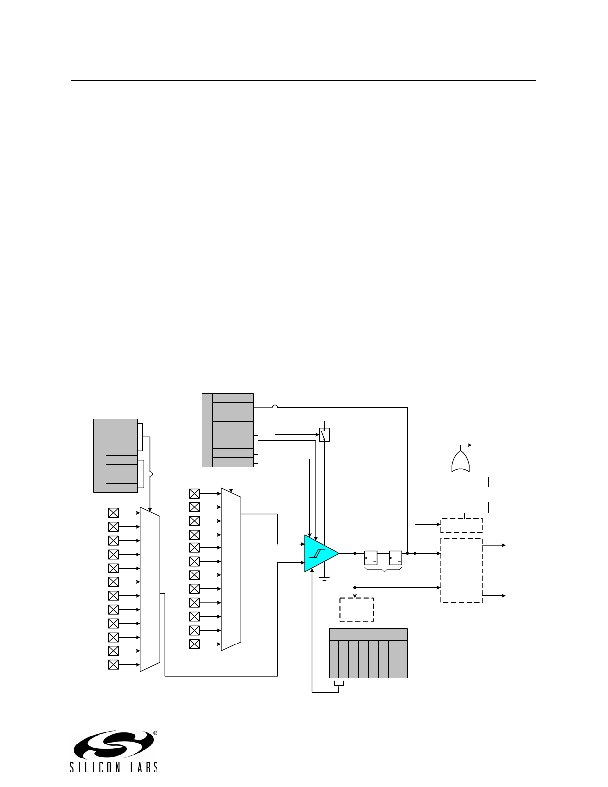
C8051F410/1/2/3
P
P
P
P
P
P
P
P
P
P
P
P
9. Comparators
C8051F41x devices include two on-chip programmable voltage comparators: Comparator0 is shown in
Figure 9.1; Comparator1 is shown in Figure 9.2. The two comparators operate identically, but only
Comparator0 can be used as a reset source.
The Comparator offers programmab le respo nse ti me and hys teres is, an ana log in put m ultiple xer, and two
outputs that are optionally av ailable at the Port pins: a synchronous “ latched” output (CP0, CP1), or an
asynchronous “raw” output (CP0A, CP1A). The asynchronous C P0A signal is available even when the
system clock is not act ive. This allo ws the Comparato r to operate and generate an output with the d evice
in STOP or SUSPEND mo de. When a ssig ned to a P ort pin , the Com parator ou tput m ay b e config ured as
open drain or push-pull (see
be used as a reset source (see Section “15.5. Comparator0 Reset” on page 130).
The Comparator0 inputs are selected in the CPT0MX register (SFR Definition 9.2). The CMX0P3-CMX0P0
bits select the Comparator0 pos itive input; the CMX0N3-CMX0N0 bits select the Comparator0 negative
input. The Comparator1 inputs are selected in the CPT1MX register (
CMX1P0 bits select the Comparator1 po sitive input; the CMX1N3-CMX1N0 bits select the Comparator1
negative input.
Important Note About Comparator Inputs: The Port pins select ed as Com parato r in puts s hou ld be con-
figured as analog inputs in their associated Port configuration register (with a ‘1’ written to the corresponding Port Latch registe r), and configured to be skip ped by the Crossbar (for details on Por t configuration,
see
Section “18.3. General Purpose Port I/O” on page 154)
Section “18.2. Port I/O Initialization” on page 151). Comparator0 may also
SFR Definition 9.4). The CMX1P3-
CP0EN
CP0OUT
CMX0N3
CMX0N2
CMX0N1
CMX0N0
CMX0P3
CPT0MX
CMX0P2
CMX0P1
CMX0P0
0.1
0.3
0.5
0.7
1.1
1.3
1.5
1.7
2.1
2.3
2.5
2.7
P0.0
P0.2
P0.4
P0.6
P1.0
P1.2
P1.4
P1.6
P2.0
P2.2
P2.4
P2.6
Figure 9.1. Comparator0 Functional Block Diagram
CP0RIF
CP0FIF
CP0HYP1
CPT0CN
CP0HYP0
CP0HYN1
CP0HYN0
CP0 +
CP0 -
Rev. 1.0 83
VDD
CP0
Interrupt
CP0
Rising-edge
Interrup t
+
-
GND
Reset
Decision
Tree
SET
SET
D
D
Q
CLR
CLR
Q
(SYNCHRONIZER)
Q
Q
Crossbar
Logic
CP0
Falling-edge
CP0
CP0A
CPT0MD
CP0MD1
CP0MD0
CP0RIE
CP0FIE
Page 84

C8051F410/1/2/3
P
P
P
P
P
P
P
P
P
P
P
P
The Comparator output can be pol led i n software, u sed a s an interru pt sourc e, in ternal o scilla tor sus pend
awakening source and /or rou ted to a P ort pin. W hen rou ted to a P ort pin, th e Comparator output i s avail
able asynchronous or synchronous to the system clock; the asynchronous output is available even in
STOP or SUSPEND mode (with no system clock active). When disabled, the Comparator output (if
assigned to a Port I/O pin via the Crossbar) defaults to the log ic low state, and its supply curren t falls to
less than 100
nA. See Section “18.1. Priority Crossbar Decoder ” on page 149 for details on configuring
Comparator outputs via the dig ital Crossbar. Comparator inputs can be externally driv en from -0.25 V to
(V
) + 0.25 V without dam age or upset. The complete Comparato r electrical specificatio ns are given in
DD
Table 9.1.
The Comparator response time may be configured in software via the CPTnMD registers (see SFR Defini-
tion 9.3 and SFR Definition 9.5). Selecting a longer response time reduces the Comparator supply current.
See Table 9.1 for complete timing and curren t consumption specifications.
CP1EN
CP1OUT
0.1
0.3
0.5
0.7
1.1
1.3
1.5
1.7
2.1
2.3
2.5
2.7
CMX1N3
CMX1N2
CMX1N1
CMX1N0
CMX1P3
CPT1MX
CMX1P2
CMX1P1
CMX1P0
P0.0
P0.2
P0.4
P0.6
P1.0
P1.2
P1.4
P1.6
P2.0
P2.2
P2.4
P2.6
CP1RIF
CP1FIF
CP1HYP1
CPT1CN
CP1HYP0
CP1HYN1
CP1HYN0
CP1 +
CP1 -
VDD
CP1
Interrup t
CP1
Rising-edge
Interrup t
Logic
+
-
GND
SET
SET
Q
D
D
CLR
CLR
Q
(SYNCHRONIZER)
Q
Q
Crossbar
CP1
Falling-edge
CP1
CP1A
CPT1MD
CP1MD1
CP1MD0
CP1RIE
CP1FIE
-
84 Rev. 1.0
Figure 9.2. Comparator1 Functional Block Diagram
Page 85

CP0+
VIN+
CP0-
VIN-
CIRCUIT CONFIGURATION
Positive Hysteresis Voltage
(Programmed with CP0HYP Bits)
VIN-
INPUTS
VIN+
OUTPUT
V
OL
Positive Hysteresis
Disabled
C8051F410/1/2/3
+
CP0
_
V
OH
OUT
Maximum
Positive Hysteresis
Negative Hysteresis
Disabled
Negative Hysteresis Voltage
(Programmed by CP0HYN Bits)
Maximum
Negative Hy steresi s
Figure 9.3. Comparator Hysteresis Plot
The Comparator hysteres is is software-programmable via its Comparator Con trol register CPTnCN (for
n
= 0 or 1). The user can program both the amount of hysteresis voltage (referred to the input voltage) and
the positive and negative-going symmetry of this hysteresis around the threshold voltage.
The Comparator hysteresis is programmed using Bits3-0 in the Comparator Control Register CPTnCN
(shown in
determined by the settings of the CPnHYN bits. As shown in Table 9.1, settings of 20, 10 or 5 mV of
negative hysteresis can be programmed, or negative hysteresis can be disabled. In a similar way, the
amount of positive hysteresis is determined by setting the CPnHYP bits.
Comparator interrupts can be generated on both rising-edge and falling-edge output transitions. (For Interrupt enable and prior ity control, see Sect ion “12. Interrupt Handler” on page 110). The CPnFIF flag is
set to logic 1 upon a C omparator fall ing-e dge det ect, an d the CPnRIF flag is set t o logi c 1 up on the C omparator rising-edge detect. Once set, these bits remain set until cleared by software. The output state of
the Comparator can be obtained at any tim e by reading the CPnOUT bit. The Comparator is enabl ed by
setting the CPnEN bit to logic 1, and is disabled by clearing this bit to logic 0.
The output state of the Comparator can be obtained at any time by reading the CPnOUT bit. The Comparator is enabled by setting the CPnEN bit to logic 1, and is disabled by cl earin g thi s bit t o lo gic 0 . Wh en th e
Comparator is enabled, the internal oscillator is awakened from SUSPEND mode if the Comparator output
is logic
SFR Definition 9.1 and SFR Definition 9.6). The amount of negative hysteresis voltage is
0.
Note that false rising ed ges a nd fa ll in g ed ges can b e d etec ted whe n th e c ompar ator i s firs t po wer ed-on or
if changes are made to the hy ste re sis o r res po ns e tim e c ontro l bi ts. Ther efore, it is recommended that the
rising-edge and falling-edge flags be explicitly cleared to logic
enabled or its mode bits have been changed. This Power Up Time is specified in
Rev. 1.0 85
0 a short time after the comparator is
Table 9.1 on page 92.
Page 86

C8051F410/1/2/3
SFR Definition 9.1. CPT0CN: Comparator0 Control
R/W R R/W R/W R/W R/W R/W R/W Reset Value
CP0EN CP0OUT CP0RIF CP0FIF CP0HYP1 CP0HYP0 CP0HYN1 CP0HYN0 00000000
Bit7 Bit6 Bit5 Bit4 Bit3 Bit2 Bit1 Bit0 SFR Address:
Bit7: CP0EN: Comparator0 Enable Bit.
0: Comparator0 Disabled.
1: Comparator0 Enabled.
Bit6: CP0OUT: Comparator0 Output State Flag.
0: Voltage on CP0+ < CP0–.
1: Voltage on CP0+ > CP0–.
Bit5: CP0RIF: Comparator0 Rising-Edge Flag.
0: No Comparator0 Rising Edge has occurred since this flag was last cleared.
1: Comparator0 Rising Edge has occurred.
Bit4: CP0FIF: Comparator0 Falling-Edge Flag.
0: No Comparator0 Falling-Edge has occurred since this flag was last cleared.
1: Comparator0 Falling-Edge has occurred.
Bits3–2: CP0HYP1–0: Comparator0 Positive Hysteresis Control Bits.
00: Positive Hysteresis Disabled.
01: Positive Hysteresis = 5 mV.
10: Positive Hysteresis = 10 mV.
11: Positive Hysteresis = 20 mV.
Bits1–0: CP0HYN1–0: Comparator0 Negative Hysteresis Control Bits.
00: Negative Hysteresis Disabled.
01: Negative Hysteresis = 5 mV.
10: Negative Hysteresis = 10 mV.
11: Negative Hysteresis = 20 mV.
0x9B
86 Rev. 1.0
Page 87

C8051F410/1/2/3
SFR Definition 9.2. CPT0MX: Comparator0 MUX Selection
R/W R/W R/W R/W R/W R/W R/W R/W Reset Value
CMX0N3 CMX0N2 CMX0N1 CMX0N0 CMX0P3 CMX0P2 CMX0P1 CMX0P0 11111111
Bit7 Bit6 Bit5 Bit4 Bit3 Bit2 Bit1 Bit0 SFR Address:
0x9F
Bits7–4: CMX0N3–CMX0N0: Comparator0 Negative Input MUX Select.
These bits select which Port pin is used as the Comparator0 negative input.
CMX0N3 CMX0N2 CMX0N1 CMX0N0 Negative Input
0000 P0.1
0001 P0.3
0010 P0.5
0011 P0.7
0100 P1.1
0101 P1.3
0110 P1.5
0111 P1.7
1000 P2.1
1001 P2.3
1010 P2.5*
1011 P2.7
11xxReserved
*Note: Available only on the C8051F410/2.
*
Bits1–0: CMX0P3–CMX0P0: Comparator0 Positive Input MUX Select.
These bits select which Port pin is used as the Comparator0 positive input.
CMX0P3 CMX0P2 CMX0P1 CMX0P0 Positive Input
0000 P0.0
0001 P0.2
0010 P0.4
0011 P0.6
0100 P1.0
0101 P1.2
0110 P1.4
0111 P1.6
1000 P2.0
1001 P2.2
1010 P2.4
1011 P2.6*
11xxReserved
*Note: Available only on the C8051F410/2.
*
Rev. 1.0 87
Page 88

C8051F410/1/2/3
SFR Definition 9.3. CPT0MD: Comparator0 Mode Selection
R/W R/W R/W R/W R/W R/W R/W R/W Reset Value
RESERVED - CP0RIE CP0FIE - - CP0MD1 CP0MD0 00000010
Bit7 Bit6 Bit5 Bit4 Bit3 Bit2 Bit1 Bit0 SFR Address:
0x9D
Bit7: RESERVED. Read = 0b. Must Write 0b.
Bit6: UNUSED. Read = 0b. Write = don’t care.
Bit5: CP0RIE: Comparator Rising-Edge Interrupt Enable.
0: Comparator rising-edge interrupt disabled.
1: Comparator rising-edge interrupt enabled.
Bit4: CP0FIE: Comparator Falling-Edge Interrupt Enable.
0: Comparator falling-edge interrupt disabled.
1: Comparator falling-edge interrupt enabled.
Bits3–2: UNUSED. Read = 00b. Write = don’t care.
Bits1–0: CP0MD1–CP0MD0: Comparator0 Mode Select
These bits select the response time for Comparator0.
Mode CP0MD1 CP0MD0 CP0 Falling Edge Response
Time (TYP)
0 0 0 Fastest Response Time
101 —
210 —
3 1 1 Lowest Power Consumption
Note: Rising Edge response times are approximately double the Falling Edge response
times.
88 Rev. 1.0
Page 89

C8051F410/1/2/3
SFR Definition 9.4. CPT1MX: Comparator1 MUX Selection
R/W R/W R/W R/W R/W R/W R/W R/W Reset Value
CMX1N3 CMX1N2 CMX1N1 CMX1N0 CMX1P3 CMX1P2 CMX1P1 CMX1P0 11111111
Bit7 Bit6 Bit5 Bit4 Bit3 Bit2 Bit1 Bit0 SFR Address:
0x9E
Bits7–4: CMX1N3–CMX1N0: Comparator1 Negative Input MUX Select.
These bits select which Port pin is used as the Comparator1 negative input.
CMX1N3 CMX1N2 CMX1N1 CMX1N0 Negative Input
0000 P0.1
0001 P0.3
0010 P0.5
0011 P0.7
0100 P1.1
0101 P1.3
0110 P1.5
0111 P1.7
1000 P2.1
1001 P2.3
1010 P2.5*
1011 P2.7
11xxReserved
*Note: Available only on the C8051F410/2.
*
Bits3–0: CMX1P3–CMX1P0: Comparator1 Positive Input MUX Select.
These bits select which Port pin is used as the Comparator1 positive input.
CMX1P3 CMX1P2 CMX1P1 CMX1P0 Positive Input
0000 P0.0
0001 P0.2
0010 P0.4
0011 P0.6
0100 P1.0
0101 P1.2
0110 P1.4
0111 P1.6
1000 P2.0
1001 P2.2
1010 P2.4
1011 P2.6*
11xxReserved
*Note: Available only on the C8051F410/2.
*
Rev. 1.0 89
Page 90

C8051F410/1/2/3
SFR Definition 9.5. CPT1MD: Comparator1 Mode Selection
R/W R/W R /W R/W R/W R/W R/W R/W Reset Value
RESERVED - CP1RIE CP1FIE - - CP1MD1 CP1MD0 00000010
Bit7 Bit6 Bit5 Bit4 Bit3 Bit2 Bit1 Bit0 SFR Address:
0x9C
Bit7: RESERVED. Read = 0b. Must Write 0b.
Bit6: UNUSED. Read = 0b. Write = don’t care.
Bit5: CP1RIE: Comparator Rising-Edge Interrupt Enable.
0: Comparator rising-edge interrupt disabled.
1: Comparator rising-edge interrupt enabled.
Bit4: CP1FIE: Comparator Falling-Edge Interrupt Enable.
0: Comparator falling-edge interrupt disabled.
1: Comparator falling-edge interrupt enabled.
Bits3–2: UNUSED. Read = 00b. Write = don’t care.
Bits1–0: CP1MD1–CP1MD0: Comparator1 Mode Select.
These bits select the response time for Comparator1.
Mode CP1MD1 CP1MD0 CP1 Falling Edge Response
Time (TYP)
0 0 0 Fastest Response Time
101 —
210 —
3 1 1 Lowest Power Consumption
Note: Rising Edge response times are approximately double the Falling Edge response
times.
90 Rev. 1.0
Page 91

C8051F410/1/2/3
SFR Definition 9.6. CPT1CN: Comparator1 Control
R/W R R/W R/W R/W R/W R /W R/W Reset Value
CP1EN CP1OUT CP1RIF CP1FIF CP1HYP1 CP1HYP0 CP1HYN1 CP1HYN0 00000000
Bit7 Bit6 Bit5 Bit4 Bit3 Bit2 Bit1 Bit0 SFR Address:
0x9A
Bit7: CP1EN: Comparator1 Enable Bit.
0: Comparator1 Disabled.
1: Comparator1 Enabled.
Bit6: CP1OUT: Comparator1 Output State Flag.
0: Voltage on CP1+ < CP1-.
1: Voltage on CP1+ > CP1-.
Bit5: CP1RIF: Comparator1 Rising-Edge Flag.
0: No Comparator1 Rising Edge has occurred since this flag was last cleared.
1: Comparator1 Rising Edge has occurred.
Bit4: CP1FIF: Comparator1 Falling-Edge Flag.
0: No Comparator1 Falling-Edge has occurred since this flag was last cleared.
1: Comparator1 Falling-Edge has occurred.
Bits3–2: CP1HYP1–0: Comparator1 Positive Hysteresis Control Bits.
00: Positive Hysteresis Disabled.
01: Positive Hysteresis = 5 mV.
10: Positive Hysteresis = 10 mV.
11: Positive Hysteresis = 20 mV.
Bits1–0: CP1HYN1–0: Comparator1 Negative Hysteresis Control Bits.
00: Negative Hysteresis Disabled.
01: Negative Hysteresis = 5 mV.
10: Negative Hysteresis = 10 mV.
11: Negative Hysteresis = 20 mV.
Rev. 1.0 91
Page 92

C8051F410/1/2/3
Table 9.1. Comparator Electrical Characteristics
VDD = 2.0 V, –40 to +85 °C unless otherwise noted. All specifications apply to both Comparator0 and Comparator1
unless otherwise noted. Typical values are given at 25
Parameter Conditions Min Typ Max Units
Response Time:
Mode 0, Vcm1 = 1.5 V
CP0+ – CP0– = 100 mV — 120 — ns
CP0+ – CP0– = –100 mV — 160 — ns
ºC.
Response Time:
Mode 1, Vcm1 = 1.5 V
Response Time:
Mode 2, Vcm1 = 1.5 V
Response Time:
Mode 3, Vcm1 = 1.5 V
Common-Mode Rejection Ratio
Positive Hysteresis 1 CP0HYP1-0 = 00 — 0.5 2.0 mV
Positive Hysteresis 2 CP0HYP1-0 = 01 2 4.5 10 mV
Positive Hysteresis 3 CP0HYP1-0 = 10 5 9.0 20 mV
Positive Hysteresis 4 CP0HYP1-0 = 11 13 18.0 40 mV
Negative Hysteresis 1 CP0HYN1-0 = 00 — –0.5 –2.0 mV
Negative Hysteresis 2 CP0HYN1-0 = 01 –2 –4.5 –10 mV
Negative Hysteresis 3 CP0HYN1-0 = 10 –5 –9.0 –20 mV
Negative Hysteresis 4 CP0HYN1-0 = 11 –13 –18.0 –40 mV
Inverting or Non-Inverting Input
Voltage Range
Input Capacitance — 4 — pF
2
CP0+ – CP0– = 100 mV — 200 — ns
CP0+ – CP0– = –100 mV — 340 — ns
CP0+ – CP0– = 100 mV — 360 — ns
CP0+ – CP0– = –100 mV — 720 — ns
CP0+ – CP0– = 100 mV — 2.2 — µs
CP0+ – CP0– = –100 mV — 7.2 — µs
— 1.5 14 mV/V
–0.25 — V
+ 0.25 V
DD
Input Bias Current — 0.5 — nA
Input Offset Voltage –10 — 10 mV
Power Supply
Power Supply R eje ct i on2
Power-up Time — 2.3 — µs
Mode 0 — 13 30 µA
Mode 1 — 6.0 20 µA
Supply Current at DC
Mode 2 — 3.0 10 µA
Mode 3 — 1.0 5 µA
Notes:
1. Vcm is the common-mode voltage on CP0+ and CP0–.
2. Guaranteed by design and/or characterization.
92 Rev. 1.0
— 0.2 4 mV/V
Page 93

C8051F410/1/2/3
10. CIP-51 Microcontroller
The MCU system controller core is the CIP-51 microcontroller. The CIP-51 is fully compatible with the
MCS-51™ instruction s et. Standard 8 03x/805x assemblers and compile rs can be used to develop soft
ware. The C8051F41x family has a superset of all the peripherals included with a standard 8051. See Section “1. System Ov erview” on page 19 for more informat ion about the a vailable peripheral s. The CIP-51
includes on-chi p d ebu g h ar dwa re wh ic h i nte rf ac es di r ect ly wi th the a nal og and di gi tal s ubsy ste ms , p rovi ding a complete data acquisition or control-system solution in a single integrated circuit.
The CIP-51 Microcont roller core implements the standar d 8051 organization and perip herals as well as
additional custo m perip herals an d functi ons to exte nd its capabil ity (see
The CIP-51 core includes the following features:
Figure 10.1 for a block diagram).
-
- Fully Compatible with MCS-51 Instruction
Set
- 50 MIPS Peak Throughput
- 256 Bytes of Internal RAM
DATA BUS
RESET
CLOCK
STOP
IDLE
D8
ACCUMULATOR
PSW
D8
BUFFER
DATA POINTER
PC INCREMENTER
PROGRAM COUNTER (PC)
PRGM. ADDRESS REG.
CONTROL
LOGIC
POWER CONTROL
REGISTER
D8
TMP1 TMP2
ALU
PIPELINE
DATA BUS
D8
D8
DATA BUS
D8
D8
D8
- Extended Interrupt Handler
- Reset Input
- Power Management Modes
- Integrated Debug Logic
D8
DATA BUS
B REGISTER
ADDRESS
REGISTER
D8
INTERFACE
D8
A16
INTERFACE
D8
INTERRUPT
INTERFACE
D8
SRAM
D8
SFR
BUS
MEMORY
STACK POINTER
SRAM
(256 X 8)
D8
SFR_ADDRESS
SFR_CONTROL
SFR_WRITE_DATA
SFR_READ_DATA
MEM_ADDRESS
MEM_CONTROL
MEM_WRITE_DATA
MEM_READ_DATA
SYSTEM_IRQs
EMULATION_IRQ
D8
Figure 10.1. CIP-51 Block Diagram
Rev. 1.0 93
Page 94

C8051F410/1/2/3
Performance
The CIP-51 employs a pipelined architecture that greatly increases its instruction throughput over the standard 8051 architecture. In a standard 8051, all i nstruction s except for MU L and DIV take 12 or 24 syste m
clock cycles to execute, and usually have a maximum syst em clock of 12
core executes 70% of its instructions in one or two syst em clock cycles , with no instruct ions taking more
than eight system clock cycles.
With the CIP-51's system clock running at 50 MHz, it has a peak throughput of 50 MIPS. The CIP-51 has a
total of 109 instructions. The table below shows the total number of instructions that require each execution
time.
Clocks to Execute 1 2 2/4 3 3/5 4 5 4/6 6 8
Number of Instructions 26 50 5 10 7 5 2 1 2 1
Programming and Debugging Support
In-system programming of the Flash program memory and communication with on-chip debug support
logic is accomplished via the Silicon Labs 2-Wire (C 2) inte rfa ce . Note th at the r e- programmable Flash can
also be read and written a singl e byte at a time by the application softwa re using the MOVC and MOVX
instructions. This feature allows program memory to be used for non-volatile data storage as well as updat
ing program code under software control.
MHz. By contrast, the CIP-51
-
The on-chip debug support logic facilitates full speed in-circuit debugging, allowing the setting of hardware
breakpoints, starting, sto pping and single steppi ng through program e xecution (includi ng interr upt servic e
routines), examination of the progra m's call stack, and reading/writin g the contents of re gisters and m em
ory. This method of on-chip debuggi ng is completely non-intrusive, requiring no RAM, Stack, timers, or
other on-chip resources.
The CIP-51 is supported by development tools from Silicon Laboratories, Inc. and third party vendors. Silicon Laboratories prov ides an inte grated de ve lopmen t enviro nment (I DE) inc luding e dit or, evaluation compiler, assembler, debugger and programmer. The IDE's debugger and programmer inte rf ac e to th e CIP-5 1
via the on-chip debug logic to provide fast and efficient in-syst em device programming and debugg ing.
Third party macro assemblers and C compilers are also available.
10.1. Instruction Set
The instruction set of the CIP-51 System Controller is fully compatible with the standard MCS-51™ instruction set. Standard 8051 development to ols can be used to develop software for the CIP-51. All CIP-51
instructions are th e binary and functional equivale nt of their MCS-51™ counterparts, inc luding opcodes,
addressing modes and effect on PSW flags. However, instruction timing is different than tha t of the stan
dard 8051.
10.1.1. Instruction and CPU Timing
In many 8051 implementations, a distinction is made between machine cycles and clock cycles, with
machine cycles varying from 2 to 12 clock cycles in length. However, the CIP-51 implementation is based
solely on clock cycle timing. All instruction timings are specified in terms of clock cycles.
-
-
Due to the pipelined archite cture of the CIP-51, most instructions execute in the same number of clock
cycles as there are program bytes in the instruction. Conditional branch instructions take two less clock
cycles to complete when the branch is not taken as opposed to when the branch is taken.
CIP-51 Instruction Set Sum mary, which inc ludes the mnemonic, number of bytes, a nd number of clock
cycles for each instruction.
94 Rev. 1.0
Table 10.1 is the
Page 95

C8051F410/1/2/3
10.1.2. MOVX Instruction and Program Memory
The MOVX instruc tio n i s ty pi ca ll y us ed to acc ess da ta stored in XDATA memory space . In th e CIP-51, the
MOVX instruction can also be u sed to wri te or erase o n-chip progr am memor y space implement ed as reprogrammable Flash m emory. The Flash access feature pro vides a mechanis m for the CIP-51 to u pdate
program code and use the program memory space for non-volatile data storage. Refer to
“16. Flash Memory” on page 135 for fu rther details.
Table 10.1. CIP-51 Instruction Set Summary1
Section
Mnemonic Description Bytes
Arithmetic Operations
ADD A, Rn Add register to A 1 1
ADD A, direct Add direct byte to A 2 2
ADD A, @Ri Add indirect RAM to A 1 2
ADD A, #data Add immediate to A 2 2
ADDC A, Rn Add register to A with carry 1 1
ADDC A, direct Add direct byte to A with carry 2 2
ADDC A, @Ri Add indirect RAM to A with carry 1 2
ADDC A, #data Add immediate to A with carry 2 2
SUBB A, Rn Subtract register from A with borrow 1 1
SUBB A, direct Subtract direct byte from A with borrow 2 2
SUBB A, @Ri Subtract indirect RAM from A with borrow 1 2
SUBB A, #data Subtract immediate from A with borrow 2 2
INC A Increment A 1 1
INC Rn Increment register 1 1
INC direct Increment direct byte 2 2
INC @Ri Increment indirect RAM 1 2
DEC A Decrement A 1 1
DEC Rn Decrement register 1 1
DEC direct Decrement direct byte 2 2
DEC @Ri Decrement indirect RAM 1 2
INC DPTR Increment Data Pointer 1 1
MUL AB Multiply A and B 1 4
DIV AB Divide A by B 1 8
DA A Decimal adjust A 1 1
Logical Operations
ANL A, Rn AND Register to A 1 1
ANL A, direct AND direct byte to A 2 2
ANL A, @Ri AND indirect RAM to A 1 2
ANL A, #data AND immediate to A 2 2
ANL direct, A AND A to direct byte 2 2
ANL direct, #data AND immediate to direct byte 3 3
ORL A, Rn OR Register to A 1 1
ORL A, direct OR direct byte to A 2 2
Notes:
1. Assumes PFEN = 1 for all instruction timing.
2. MOVC instructions take 4 to 7 clock cycles depending on instruction alignment and the FLRT setting (SFR
Definition 16.3. FLSCL: Flash Scale).
Clock
Cycles
Rev. 1.0 95
Page 96

C8051F410/1/2/3
Table 10.1. CIP-51 Instruction Set Summary1 (Continued)
Mnemonic Description Bytes
ORL A, @Ri OR indirect RAM to A 1 2
ORL A, #data OR immediate to A 2 2
ORL direct, A OR A to direct byte 2 2
ORL direct, #data OR immediate to direct byte 3 3
XRL A, Rn Exclusive-OR Register to A 1 1
XRL A, direct Exclusive-OR direct byte to A 2 2
XRL A, @Ri Exclusive-OR indirect RAM to A 1 2
XRL A, #data Exclusive-OR immediate to A 2 2
XRL direct, A Exclusive-OR A to direct byte 2 2
XRL direct, #data Exclusive-OR immediate to direct byte 3 3
CLR A Clear A 1 1
CPL A Complement A 1 1
RL A Rotate A left 1 1
RLC A Rotate A left through Carry 1 1
RR A Rotate A right 1 1
RRC A Rotate A right through Carry 1 1
SWAP A Swap nibbles of A 1 1
Data Transfer
MOV A, Rn Move Register to A 1 1
MOV A, direct Move direct byte to A 2 2
MOV A, @Ri Move indirect RAM to A 1 2
MOV A, #data Move imm edi ate to A 2 2
MOV Rn, A Move A to Register 1 1
MOV Rn, direct Move direct byte to Register 2 2
MOV Rn, #data Move immediate to Register 2 2
MOV direct, A Move A to direct byte 2 2
MOV direct, Rn Move Register to direct byte 2 2
MOV direct, direct Move direct byte to direct byte 3 3
MOV direct, @Ri Move indirect RAM to direct byte 2 2
MOV direct, #data Move immediate to direct byte 3 3
MOV @Ri, A Move A to indirect RAM 1 2
MOV @Ri, direct Move direct byte to indirect RAM 2 2
MOV @Ri, #data Move immediate to indirec t RAM 2 2
MOV DPTR, #data16 Load DPTR with 16-bit constant 3 3
MOVC A, @A+DPTR Move code byte relative DPTR to A 1
MOVC A, @A+PC Move code byte relative PC to A 1
MOVX A, @Ri Move external data (8-bit address) to A 1 3
MOVX @Ri, A Move A to external data (8-bit address) 1 3
MOVX A, @DPTR Move external data (16-bit address) to A 1 3
MOVX @DPTR, A Move A to external data (16-bit address) 1 3
PUSH direct Push direct byte onto stack 2 2
Notes:
1. Assumes PFEN = 1 for all instruction timing.
2. MOVC instructions take 4 to 7 clock cycles depending on instruction alignment and the FLRT setting (SFR
Definition 16.3. FLSCL: Flash Scale).
Clock
Cycles
4 to 7
4 to 7
2
2
96 Rev. 1.0
Page 97

C8051F410/1/2/3
Table 10.1. CIP-51 Instruction Set Summary1 (Continued)
Mnemonic Description Bytes
POP direct Pop direct byte from stack 2 2
XCH A, Rn Exchange Register with A 1 1
XCH A, direct Exchange direct byte with A 2 2
XCH A, @Ri Exchange indirect RAM with A 1 2
XCHD A, @Ri Exchange low nibble of indirect RAM with A 1 2
Boolean Manipulation
CLR C Clear Carry 1 1
CLR bit Clear direct bit 2 2
SETB C Set Carry 1 1
SETB bit Set direct bit 2 2
CPL C Complement Carry 1 1
CPL bit Complement direct bit 2 2
ANL C, bit AND direct bit to Carry 2 2
ANL C, /bit AND complement of direct bit to Carry 2 2
ORL C, bit OR direct bit to carry 2 2
ORL C, /bit OR complement of direct bit to Carry 2 2
MOV C, bit Move direct bit to Carry 2 2
MOV bit, C Move Carry to direct bit 2 2
JC rel Jump if Carry is set 2 2/4
JNC rel Jump if Carry is not set 2 2/4
JB bit, rel Jump if direct bit is set 3 3/5
JNB bit, rel Jump if direct bit is not set 3 3/5
JBC bit, rel Jump if direct bit is set and clear bit 3 3/5
Program Branching
ACALL addr11 Absolute subroutine call 2 4
LCALL addr16 Long subroutine call 3 5
RET Return from subroutine 1 6
RETI Return from interrupt 1 6
AJMP addr11 Absolute jump 2 4
LJMP addr16 Long jump 3 5
SJMP rel Short jump (relative address) 2 4
JMP @A+DPTR Jump indirect relative to DPTR 1 4
JZ rel Jump if A equals zero 2 2/4
JNZ rel Jump if A does not equal zero 2 2/4
CJNE A, direct, rel Compare direct byte to A and jump if not equal 3 3/5
CJNE A, #data, rel Compare immediate to A and jump if not equal 3 3/5
CJNE Rn, #data, rel Compare immediate to Register and jump if not equal 3 3/5
CJNE @Ri, #data, rel Compare immediate to indirect and jump if not equal 3 4/6
DJNZ Rn, rel Decrement Register and jump if not zero 2 2/4
DJNZ direct, rel Decrement direct byte and jump if not zero 3 3/5
NOP No operation 1 1
Notes:
1. Assumes PFEN = 1 for all instruction timing.
2. MOVC instructions take 4 to 7 clock cycles depending on instruction alignment and the FLRT setting (SFR
Definition 16.3. FLSCL: Flash Scale).
Clock
Cycles
Rev. 1.0 97
Page 98

C8051F410/1/2/3
Notes on Registers, Operands and Addressing Modes:
- Register R0-R7 of the currently selected register bank.
Rn
@Ri - Data RAM location addressed indirectly through R0 or R1.
rel - 8-bit, signed (two’s complement) offset relative to the first byte of the following instruction. Used by
SJMP and all conditional jumps.
direct - 8-bit internal data location’s address. This could be a direct-access Data RAM location (0x00-
0x7F) or an SFR (0x80-0xFF).
#data - 8-bit constant
#data16 - 16-bit constant
bit - Direct-accessed bit in Data RAM or SFR
addr11 - 11-bit destination address used by ACALL and AJMP . The destination must be within the same
2K-byte page of program memory as the first byte of the following instruction.
addr16 - 16-bit destination address used by LCALL and LJMP. The destination may be anywhere within
the 8K-byte program memory space.
There is one unused opcode (0xA5) that performs the same function as NOP.
All mnemonics copyrighted © Intel Corporation 1980.
10.2. Register Descriptions
Following are descriptions of SFRs related to the operation of the CIP-51 System Controller. Reserved bits
should not be set to lo gic
which case the res et valu e of t he bit will be log ic
tions of the remaining SFRs are included in the sections of the datasheet associated with their corresponding system function.
1. Future product v ersions may use these bits to implement new feature s in
0, selecting the feature's defaul t state. Detailed descrip-
SFR Definition 10.1. SP: Stack Pointe r
R/W R/W R/W R/W R/W R/W R/W R/W Reset V alue
00000111
Bit7 Bit6 Bit5 Bit4 Bit3 Bit2 Bit1 Bit0
SFR Address: 0x81
Bits7–0: SP: Stack Pointer.
The Stack Pointer holds the location of the top of the stack. The stack pointer is incremented
before every PUSH operation. The SP register defaults to 0x07 after reset.
98 Rev. 1.0
Page 99

C8051F410/1/2/3
SFR Definition 10.2. DPL: Data Pointer Low Byte
R/W R/W R/W R/W R/W R/W R/W R/W Reset Value
00000000
Bit7 Bit6 Bit5 Bit4 Bit3 Bit2 Bit1 Bit0
SFR Address: 0x82
Bits7–0: DPL: Data Pointer Low.
The DPL register is the low byte of the 16-bit DPTR. DPTR is used to access indirectly
addressed XRAM and Flash memory.
SFR Definition 10.3. DPH: Data Pointer High Byte
R/W R/W R/W R/W R/W R/W R/W R/W Reset Value
00000000
Bit7 Bit6 Bit5 Bit4 Bit3 Bit2 Bit1 Bit0
SFR Address: 0x83
Bits7–0: DPH: Data Pointer High.
The DPH register is the high byte of the 16-bit DPTR. DPTR is used to access indirectly
addressed XRAM and Flash memory.
Rev. 1.0 99
Page 100

C8051F410/1/2/3
SFR Definition 10.4. PSW: Program Status Word
R/W R/W R/W R/W R/W R/W R/W R Reset Value
CY AC F0 RS1 RS0 OV F1 PARITY 00000000
Bit7 Bit6 Bit5 Bit4 Bit3 Bit2 Bit1 Bit0
SFR Address: 0xD0
Bit7: CY: Carry Flag.
This bit is set when the last arithmetic operation resulted in a carry (addition) or a borrow
(subtraction). It is cleared to 0 by all other arithmetic operations.
Bit6: AC: Auxiliary Carry Flag
This bit is set when the last arithmetic operation resulted in a carry into (addition) or a borrow
from (subtraction) the high order nibble. It is cleared to 0 by all other arithmetic operations.
Bit5: F0: User Flag 0.
This is a bit-addressable, general purpose flag for use under software control.
Bits4–3: RS1–RS0: Register Bank Sel ec t.
These bits select which register bank is used during register accesses.
RS1 RS0 Register Bank Address
0 0 0 0x00–0x07
0 1 1 0x08–0x0F
1 0 2 0x10–0x17
1 1 3 0x18–0x1F
Bit
Addressable
Bit2: OV: Overflow Flag.
This bit is set to 1 under the following circumstances:
• An ADD, ADDC, or SUBB instruction causes a sign-change overflow.
• A MUL instruction results in an overflow (result is greater than 255).
• A DIV instruction causes a divide-by-zero condition.
The OV bit is cleared to 0 by the ADD, ADDC, SUBB, MUL, and DIV instructions in all other
cases.
Bit1: F1: User Flag 1.
This is a bit-addressable, general purpose flag for use under software control.
Bit0: PARITY: Parity Flag.
This bit is set to 1 if the sum of the eight bits in the accumulator is odd and cleared if the sum
is even.
100 Rev. 1.0
 Loading...