

Page 1
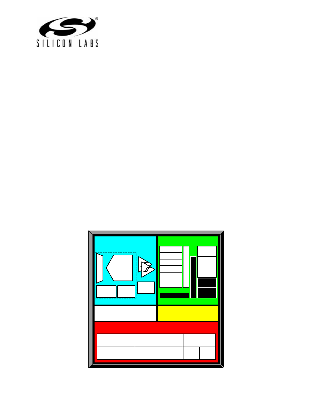
C8051F340/1/2/3/4/5/6/7/8/9/A/B/C/D
ANALOG
PERIPHERALS
10-bit
200 ksps
ADC
64/32 kB
ISP FLASH
4/2 kB RAM
POR
DEBUG
CIRCUITRY
FLEXIBLE
INTERRUPTS
8051 CPU
(48/25 MIPS)
DIGITAL I/O
PRECISION INTERNAL
OSCILLATORS
HIGH-SPEED CONTROLLER CORE
A
M
U
X
CROSSBAR
+
-
WDT
+
-
USB Controller /
Transceiver
Port 0
Port 1
Port 2
Port 3
TEMP
SENSOR
VREG
VREF
Port 4
Ext. Memory I/F
48 Pin Only
UART0
SMBus
PCA
4 Timers
SPI
UART1*
C8051F340/1/2/34/5/6/7/A/B Only * C8051F340/1/4/5/8/A/B/C Only
Full Speed USB Flash MCU Family
Analog Peripherals
- 10-Bit ADC (C8051F340/1/2/3/4/5/6/7/A/B only)
• Up to 200 ksps
• Built-in analog multiplexer with single-ended and
differential mode
• VREF from external pin, internal reference, or V
• Built-in temperature sensor
• External conversion start input option
DD
- Two comparators
- Internal voltage reference
(C8051F340/1/2/3/4/5/6/7/A/B only)
- Brown-out detector and POR Circuitry
USB Function Controller
-
USB specification 2.0 compliant
- Full speed (12 Mbps) or low speed (1.5 Mbps) operation
- Integrated clock recovery; no external crystal required for
full speed or low speed
- Supports eight flexible endpoints
- 1 kB USB buffer memory
- Integrated transceiver; no external resistors required
On-Chip Debug
-
On-chip debug circuitry facilitates full speed, non-intrusive in-system debug (No emulator required)
- Provides breakpoints, single stepping,
inspect/modify memory and registers
- Superior performance to emulation systems using
ICE-chips, target pods, and sockets
Voltage Supply Input: 2.7 to 5.25 V
-
Voltages from 3.6 to 5.25 V supported using On-Chip
Voltage Regulator
HIgh Speed 8051 µC Core
-
Pipelined instruction architecture; executes 70% of
Instructions in 1 or 2 system clocks
- 48 MIPS and 25 MIPS versions available.
- Expanded interrupt handler
Memory
-
4352 or 2304 Bytes RAM
- 64 or 32 kB Flash; In-system programmable in 512-byte
sectors
Digital Peripherals
-
40/25 Port I/O; All 5 V tolerant with high sink current
- Hardware enhanced SPI™, SMBus™, and one or two
enhanced UART serial ports
- Four general purpose 16-bit counter/timers
- 16-bit programmable counter array (PCA) with five cap-
ture/compare modules
- External Memory Interface (EMIF)
Clock Sources
-
Internal Oscillator: ±0.25% accuracy with clock recovery
enabled. Supports all USB and UART modes
- External Oscillator: Crystal, RC, C, or clock (1 or 2 Pin
modes)
- Low Frequency (80 kHz) Internal Oscillator
- Can switch between clock sources on-the-fly
Packages
-
48-pin TQFP (C8051F340/1/4/5/8/C)
- 32-pin LQFP (C8051F342/3/6/7/9/A/B/D)
- 5x5 mm 32-pin QFN (C8051F342/3/6/7/9/A/B)
Temperature Range: –40 to +85 °C
Rev. 1.4 9/09 Copyright © 2009 by Silicon Laboratories C8051F34x
Page 2

C8051F340/1/2/3/4/5/6/7/8/9/A/B/C/D
2 Rev. 1.4
Page 3

C8051F340/1/2/3/4/5/6/7/8/9/A/B/C/D
Table of Contents
1. System Overview.................................................................................................... 17
2. Absolute Maximum Ratings .................................................................................. 24
3. Global DC Electrical Characteristics.................................................................... 25
4. Pinout and Package Definitions............................................................................ 28
5. 10-Bit ADC (ADC0, C8051F340/1/2/3/4/5/6/7/A/B Only)........................................ 41
5.1. Analog Multiplexer ............................................................................................ 42
5.2. Temperature Sensor......................................................................................... 43
5.3. Modes of Operation .......................................................................................... 45
5.3.1. Starting a Conversion............................................................................... 45
5.3.2. Tracking Modes . ....................................................................................... 46
5.3.3. Settling Time Requirements..................................................................... 47
5.4. Programmable Window Detector...................................................................... 52
5.4.1. Window Detector In Single-Ended Mode ................................................. 54
5.4.2. Window Detector In Differential Mode...................................................... 55
6. Voltage Reference (C8051F340/1/2/3/4/5/6/7/A/B Only)....................................... 57
7. Comparators........................................................................................................... 59
8. Voltage Regulator (REG0)...................................................................................... 69
8.1. Regulator Mode Selection................................................................................. 69
8.2. VBUS Detection................................................................................................ 69
9. CIP-51 Microcontroller........................................................................................... 73
9.1. Instruction Set................................................................................................... 74
9.1.1. Instruction and CPU Timing ..................................................................... 74
9.1.2. MOVX Instruction and Program Memory ................................................. 75
9.2. Memory Organization........................................................................................ 79
9.2.1. Program Memory...................................................................................... 80
9.2.2. Data Memory............................................................................................ 81
9.2.3. General Purpose Registers...................................................................... 81
9.2.4. Bit Addressable Locations........................................................................ 81
9.2.5. Stack ....................................................................................................... 81
9.2.6. Special Function Registers....................................................................... 82
9.2.7. Register Descriptions............................................................................... 86
9.3. Interrupt Handler............................................................................................... 88
9.3.1. MCU Interrupt Sources and Vectors ........................................................ 88
9.3.2. External Interrupts.................................................................................... 88
9.3.3. Interrupt Priorities..................................................................................... 89
9.3.4. Interrupt Latency ......................................................................................
9.3.5. Interrupt Register Descriptions................................................................. 90
9.4. Power Management Modes.............................................................................. 97
9.4.1. Idle Mode.................................................................................................. 97
9.4.2. Stop Mode................................................................................................ 97
10.Prefetch Engine ...................................................................................................... 99
11.Reset Sources....................................................................................................... 100
11.1.Power-On Reset............................................................................................. 101
89
Rev. 1.3 3
Page 4

C8051F340/1/2/3/4/5/6/7/8/9/A/B/C/D
11.2.Power-Fail Reset / VDD Monitor .................................................................... 102
11.3.External Reset................................................................................................ 103
11.4.Missing Clock Detector Reset ........................................................................ 103
11.5.Comparator0 Reset........................................................................................ 103
11.6.PCA Watchdog Timer Reset .......................................................................... 103
11.7.Flash Error Reset ........................................................................................... 103
11.8.Software Reset............................................................................................... 104
11.9.USB Reset . ..................................................................................................... 104
12.Flash Memory ....................................................................................................... 107
12.1.Programming The Flash Memory................................................................... 107
12.1.1.Flash Lock and Key Functions............................................................... 107
12.1.2.Flash Erase Procedure .......................................................................... 107
12.1.3.Flash Write Procedure ........................................................................... 108
12.2.Non-Volatile Data Storage.............................................................................. 109
12.3.Security Options............................................................................................. 109
13.External Data Memory Interface and On-Chip XRAM........................................ 114
13.1.Accessing XRAM............................................................................................ 114
13.1.1.16-Bit MOVX Example........................................................................... 114
13.1.2.8-Bit MOVX Example............................................................................. 114
13.2.Accessing USB FIFO Space .......................................................................... 115
13.3.Configuring the External Memory Interface.................................................... 116
13.4.Port Configuration........................................................................................... 116
13.5.Multiplexed and Non-multiplexed Selection.................................................... 119
13.5.1.Multiplexed Configuration....................................................................... 119
13.5.2.Non-multiplexed Configuration............................................................... 120
13.6.Memory Mode Selection................................................................................. 120
13.6.1.Internal XRAM Only ............................................................................... 121
13.6.2.Split Mode without Bank Select.............................................................. 121
13.6.3.Split Mode with Bank Select................................................................... 122
13.6.4.External Only.......................................................................................... 122
13.7.Timing .......................................................................................................... 122
13.7.1.Non-multiplexed Mode........................................................................... 124
13.7.2.Multiplexed Mode................................................................................... 127
14.Oscillators............................................................................................................. 131
14.1.Programmable Internal High-F
14.1.1.Internal H-F Oscillator Suspend Mode................................................... 132
14.2.Programmable Internal Low-Frequency (L-F) Oscillator ................................ 133
14.2.1.Calibrating the Internal L-F Oscillator..................................................... 133
14.3.External Oscillator Drive Circuit...................................................................... 135
14.3.1.Clocking Timers Directly Through the External Oscillator...................... 135
14.3.2.External Crystal Example....................................................................... 135
14.3.3.External RC Example............................................................................. 136
14.3.4.External Capacitor Example................................................................... 136
14.4.4x Clock Multiplier .......................................................................................... 138
14.5.System and USB Clock Selection .................................................................. 139
requency (H-F) Oscillator............................... 132
4 Rev. 1.3
Page 5

C8051F340/1/2/3/4/5/6/7/8/9/A/B/C/D
14.5.1.System Clock Selection ......................................................................... 139
14.5.2.USB Clock Selection.............................................................................. 139
15.Port Input/Output.................................................................................................. 142
15.1.Priority Crossbar Decoder.............................................................................. 144
15.2.Port I/O Initialization ....................................................................................... 147
15.3.General Purpose Port I/O............................................................................... 150
16.Universal Serial Bus Controller (USB0).............................................................. 159
16.1.Endpoint Addressing ...................................................................................... 160
16.2.USB Transceiver ............................................................................................ 160
16.3.USB Register Access..................................................................................... 162
16.4.USB Clock Configuration................................................................................ 166
16.5.FIFO Management ......................................................................................... 167
16.5.1.FIFO Split Mode..................................................................................... 167
16.5.2.FIFO Double Buffering........................................................................... 168
16.5.3.FIFO Access .......................................................................................... 168
16.6.Function Addressing....................................................................................... 169
16.7.Function Configuration and Control................................................................ 169
16.8.Interrupts ........................................................................................................ 172
16.9.The Serial Interface Engine............................................................................ 176
16.10.Endpoint0 ..................................................................................................... 176
16.10.1.Endpoint0 SETUP Transactions .......................................................... 177
16.10.2.Endpoint0 IN Transactions................................................................... 177
16.10.3.Endpoint0 OUT Transactions............................................................... 178
16.11.Configuring Endpoints1-3............................................................................. 180
16.12.Controlling Endpoints1-3 IN.......................................................................... 180
16.12.1.Endpoints1-3 IN Interrupt or Bulk Mode............................................... 180
16.12.2.Endpoints1-3 IN Isochronous Mode..................................................... 181
16.13.Controlling Endpoints1-3 OUT...................................................................... 183
16.13.1.Endpoints1-3 OUT Interrupt or Bulk Mode........................................... 183
16.13.2.Endpoints1-3 OUT Isochronous Mode................................................. 184
17.SMBus ................................................................................................................... 188
17.1.Supporting Documents................................................................................... 189
17.2.SMBus Configuration...................................................................................... 189
17.3.SMBus Operation...........................................................................................
17.3.1.Arbitration............................................................................................... 190
17.3.2.Clock Low Extension.............................................................................. 191
17.3.3.SCL Low Timeout................................................................................... 191
17.3.4.SCL High (SMBus Free) Timeout .......................................................... 191
17.4.Using the SMBus............................................................................................ 191
17.4.1.SMBus Configuration Register............................................................... 192
17.4.2.SMB0CN Control Register..................................................................... 195
17.4.3.Data Register......................................................................................... 198
17.5.SMBus Transfer Modes.................................................................................. 198
17.5.1.Master Transmitter Mode....................................................................... 198
17.5.2.Master Receiver Mode........................................................................... 200
189
Rev. 1.3 5
Page 6

C8051F340/1/2/3/4/5/6/7/8/9/A/B/C/D
17.5.3.Slave Receiver Mode............................................................................. 201
17.5.4.Slave Transmitter Mode......................................................................... 202
17.6.SMBus Status Decoding................................................................................. 202
18.UART0.................................................................................................................... 205
18.1.Enhanced Baud Rate Generation................................................................... 206
18.2.Operational Modes......................................................................................... 206
18.2.1.8-Bit UART............................................................................................. 207
18.2.2.9-Bit UART............................................................................................. 208
18.3.Multiprocessor Communications .................................................................... 208
19.UART1 (C8051F340/1/4/5/8/A/B/C Only).............................................................. 213
19.1.Baud Rate Generator ..................................................................................... 214
19.2.Data Format.................................................................................................... 215
19.3.Configuration and Operation .......................................................................... 216
19.3.1.Data Transmission................................................................................. 216
19.3.2.Data Reception ...................................................................................... 216
19.3.3.Multiprocessor Communications............................................................ 217
20.Enhanced Serial Peripheral Interface (SPI0)...................................................... 222
20.1.Signal Descriptions......................................................................................... 223
20.1.1.Master Out, Slave In (MOSI).................................................................. 223
20.1.2.Master In, Slave Out (MISO).................................................................. 223
20.1.3.Serial Clock (SCK)................................................................................. 223
20.1.4.Slave Select (NSS) ................................................................................ 223
20.2.SPI0 Master Mode Operation......................................................................... 224
20.3.SPI0 Slave Mode Operation........................................................................... 226
20.4.SPI0 Interrupt Sources................................................................................... 226
20.5.Serial Clock Timing......................................................................................... 227
20.6.SPI Special Function Registers...................................................................... 229
21.Timers.................................................................................................................... 235
21.1.Timer 0 and Timer 1....................................................................................... 235
21.1.1.Mode 0: 13-bit Counter/Timer................................................................ 235
21.1.2.Mode 1: 16-bit Counter/Timer................................................................ 236
21.1.3.Mode 2: 8-bit Counter/Timer with Auto-Reload...................................... 237
21.1.4.Mode 3: Two 8-bit Counter/Timers (Timer 0 Only)................................. 238
21.2.Timer 2 ..........................................................................................................
21.2.1.16-bit Timer with Auto-Reload................................................................ 243
21.2.2.8-bit Timers with Auto-Reload................................................................ 244
21.2.3.Timer 2 Capture Modes: USB Start-of-Frame or LFO Falling Edge...... 245
21.3.Timer 3 .......................................................................................................... 249
21.3.1.16-bit Timer with Auto-Reload................................................................ 249
21.3.2.8-bit Timers with Auto-Reload................................................................ 250
21.3.3.USB Start-of-Frame Capture.................................................................. 251
22.Programmable Counter Array (PCA0)................................................................ 255
22.1.PCA Counter/Timer........................................................................................ 256
22.2.Capture/Compare Modules ............................................................................ 257
22.2.1.Edge-triggered Capture Mode................................................................ 258
243
6 Rev. 1.3
Page 7

C8051F340/1/2/3/4/5/6/7/8/9/A/B/C/D
22.2.2.Software Timer (Compare) Mode........................................................... 259
22.2.3.High Speed Output Mode....................................................................... 260
22.2.4.Frequency Output Mode ........................................................................ 261
22.2.5.8-Bit Pulse Width Modulator Mode......................................................... 262
22.2.6.16-Bit Pulse Width Modulator Mode....................................................... 263
22.3.Watchdog Timer Mode................................................................................... 264
22.3.1.Watchdog Timer Operation.................................................................... 264
22.3.2.Watchdog Timer Usage ......................................................................... 265
22.4.Register Descriptions for PCA........................................................................ 266
23.C2 Interface........................................................................................................... 271
23.1.C2 Interface Registers.................................................................................... 271
23.2.C2 Pin Sharing ............................................................................................... 273
Document Change List............................................................................................. 274
Contact Information.................................................................................................. 276
Rev. 1.3 7
Page 8

C8051F340/1/2/3/4/5/6/7/8/9/A/B/C/D
List of Figures
1. System Overview
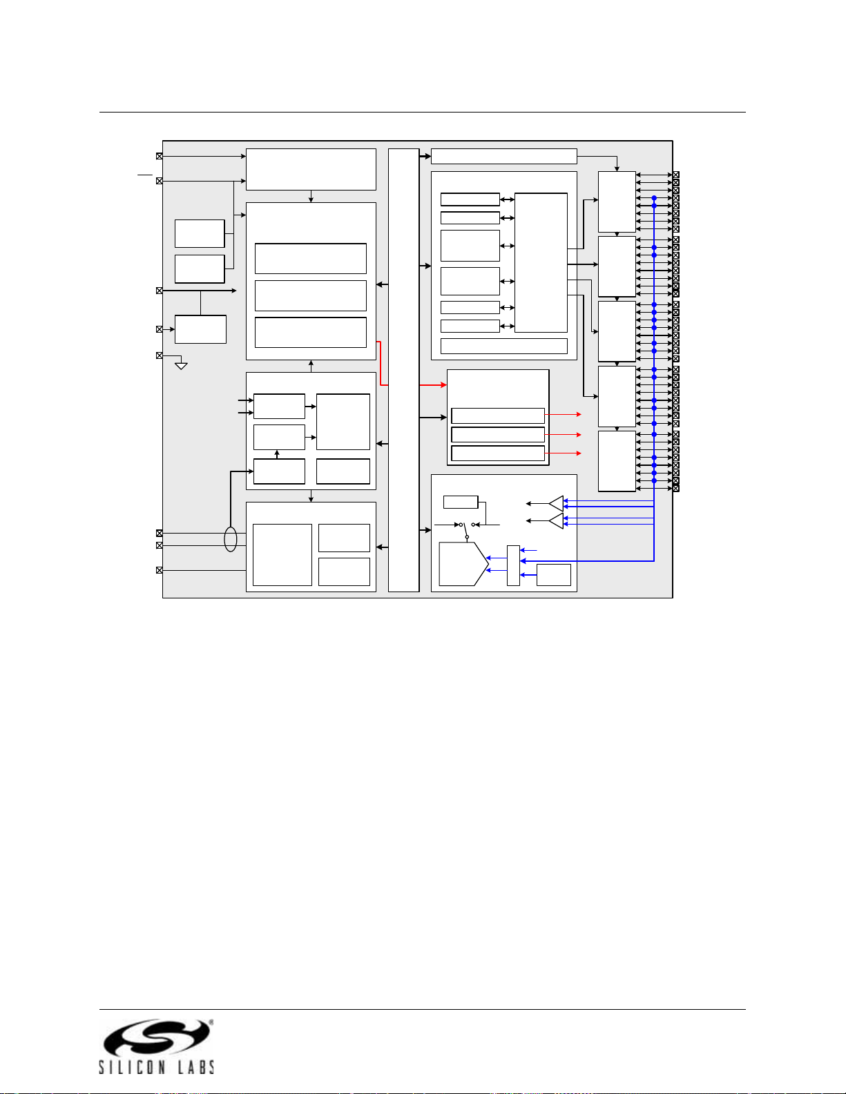
Figure 1.1. C8051F340/1/4/5 Block Diagram........................................................... 19
Figure 1.2. C8051F342/3/6/7 Block Diagram........................................................... 20
Figure 1.3. C8051F348/C Block Diagram................................................................. 21
Figure 1.4. C8051F349/D Block Diagram................................................................. 22
Figure 1.5. C8051F34A/B Block Diagram ................................................................ 23
4. Pinout and Package Definitions
Figure 4.1. TQFP-48 Pinout Diagram (Top View) .................................................... 31
Figure 4.2. TQFP-48 Package Diagram................................................................... 32
Figure 4.3. TQFP-48 Recommended PCB Land Pattern......................................... 33
Figure 4.4. LQFP-32 Pinout Diagram (Top View)..................................................... 34
Figure 4.5. LQFP-32 Package Diagram................................................................... 35
Figure 4.6. LQFP-32 Recommended PCB Land Pattern ......................................... 36
Figure 4.7. QFN-32 Pinout Diagram (Top View) ...................................................... 37
5. 10-Bit ADC (ADC0, C8051F340/1/2/3/4/5/6/7/A/B Only)
Figure 5.1. ADC0 Functional Block Diagram............................................................ 41
Figure 5.2. Temperature Sensor Transfer Function................................................. 43
Figure 5.3. Temperature Sensor Error with 1-Point Calibration (VREF = 2.40 V).... 44
Figure 5.4. 10-Bit ADC Track and Conversion Example Timing .............................. 46
Figure 5.5. ADC0 Equivalent Input Circuits.............................................................. 47
Figure 5.6. ADC Window Compare Example: Right-Justified Single-Ended Data... 54
Figure 5.7. ADC Window Compare Example: Left-Justified Single-Ended Data...... 54
Figure 5.8. ADC Window Compare Example: Right-Justified Differential Data........ 55
Figure 5.9. ADC Window Compare Example: Left-Justified Differential Data.......... 55
6. Voltage Reference (C8051F340/1/2/3/4/5/6/7/A/B Only)
Figure 6.1. Voltage Reference Functional Block Diagram........................................ 57
7. Comparators
Figure 7.1. Comparator Functional Block Diagram .................................................. 60
Figure 7.2. Comparator Hysteresis Plot ................................................................... 61
8. Voltage Regulator (REG0)
Figure 8.1. REG0 Configuration: USB Bus-Powered............................................... 70
Figure 8.2. REG0 Configuration: USB Self-Powered............................................... 70
Figure 8.3. REG0 Configuration: USB Self-Powered, Regulator Disabled............... 71
Figure 8.4. REG0 Configuration: No USB Connection............................................. 71
9. CIP-51 Microcontroller
Figure 9.1. CIP-51 Block Diagram............................................................................ 73
Figure 9.2. On-Chip Memory Map for 64 kB Devices............................................... 79
Figure 9.3. On-Chip Memory Map for 32 kB Devices............................................... 80
11. Reset Sources
Figure 11.1. Reset Sources.................................................................................... 100
Figure 11.2. Power-On and VDD Monitor Reset Timing ........................................ 101
8 Rev. 1.3
Page 9

C8051F340/1/2/3/4/5/6/7/8/9/A/B/C/D
12. Flash Memory
Figure 12.1. Flash Program Memory Map and Security Byte................................. 110
13. External Data Memory Interface and On-Chip XRAM
Figure 13.1. USB FIFO Space and XRAM Memory Map
with USBFAE set to ‘1’...................................................................................... 115
Figure 13.2. Multiplexed Configuration Example.................................................... 119
Figure 13.3. Non-multiplexed Configuration Example............................................ 120
Figure 13.4. EMIF Operating Modes...................................................................... 120
Figure 13.5. Non-multiplexed 16-bit MOVX Timing................................................ 124
Figure 13.6. Non-multiplexed 8-bit MOVX without Bank Select Timing ................. 125
Figure 13.7. Non-multiplexed 8-bit MOVX with Bank Select Timing ...................... 126
Figure 13.8. Multiplexed 16-bit MOVX Timing........................................................ 127
Figure 13.9. Multiplexed 8-bit MOVX without Bank Select Timing......................... 128
Figure 13.10. Multiplexed 8-bit MOVX with Bank Select Timing............................ 129
14. Oscillators
Figure 14.1. Oscillator Diagram.............................................................................. 131
15. Port Input/Output
Figure 15.1. Port I/O Functional Block Diagram (Port 0 through Port 3)................ 142
Figure 15.2. Port I/O Cell Block Diagram ............................................................... 143
Figure 15.3. Peripheral Availability on Port I/O Pins............................................... 144
Figure 15.4. Crossbar Priority Decoder in Example Configuration
(No Pins Skipped)............................................................................................. 145
Figure 15.5. Crossbar Priority Decoder in
Example Configuration (3 Pins Skipped) .......................................................... 146
16. Universal Serial Bus Controller (USB0)
Figure 16.1. USB0 Block Diagram.......................................................................... 159
Figure 16.2. USB0 Register Access Scheme......................................................... 162
Figure 16.3. USB FIFO Allocation.......................................................................... 167
17. SMBus
Figure 17.1. SMBus Block Diagram ....................................................................... 188
Figure 17.2. Typical SMBus Configuration............................................................. 189
Figure 17.3. SMBus Transaction............................................................................ 190
Figure 17.4. Typical SMBus SCL Generation......................................................... 193
Figure 17.5. Typical Master Transmitter Sequence................................................ 199
Figure 17.6. Typical Master Receiver Sequence.................................................... 200
Figure 17.7. Typical Slave Receiver Sequence...................................................... 201
Figure 17.8. Typical Slave Transmitter Sequence.................................................. 202
18. UART0
Figure 18.1. UART0 Block Diagram....................................................................... 205
Figure 18.2. UART0 Baud Rate Logic.................................................................... 206
Figure 18.3. UART Interconnect Diagram.............................................................. 207
Figure 18.4. 8-Bit UART Timing Diagram............................................................... 207
Figure 18.5. 9-Bit UART Timing Diagram............................................................... 208
Figure 18.6. UART Multi-Processor Mode Interconnect Diagram.......................... 209
19. UART1 (C8051F340/1/4/5/8/A/B/C Only)
Rev. 1.3 9
Page 10

C8051F340/1/2/3/4/5/6/7/8/9/A/B/C/D
Figure 19.1. UART1 Block Diagram....................................................................... 213
Figure 19.2. UART1 Timing Without Parity or Extra Bit.......................................... 215
Figure 19.3. UART1 Timing With Parity ................................................................. 215
Figure 19.4. UART1 Timing With Extra Bit............................................................. 215
Figure 19.5. Typical UART Interconnect Diagram.................................................. 216
Figure 19.6. UART Multi-Processor Mode Interconnect Diagram.......................... 218
20. Enhanced Serial Peripheral Interface (SPI0)
Figure 20.1. SPI Block Diagram............................................................................. 222
Figure 20.2. Multiple-Master Mode Connection Diagram....................................... 225
Figure 20.3. 3-Wire Single Master and Slave Mode Connection Diagram............. 225
Figure 20.4. 4-Wire Single Master Mode and Slave Mode Connection Diagram... 225
Figure 20.5. Master Mode Data/Clock Timing........................................................ 227
Figure 20.6. Slave Mode Data/Clock Timing (CKPHA = 0).................................... 228
Figure 20.7. Slave Mode Data/Clock Timing (CKPHA = 1).................................... 228
Figure 20.8. SPI Master Timing (CKPHA = 0)........................................................ 232
Figure 20.9. SPI Master Timing (CKPHA = 1)........................................................ 232
Figure 20.10. SPI Slave Timing (CKPHA = 0)........................................................ 233
Figure 20.11. SPI Slave Timing (CKPHA = 1)........................................................ 233
21. Timers
Figure 21.1. T0 Mode 0 Block Diagram.................................................................. 236
Figure 21.2. T0 Mode 2 Block Diagram.................................................................. 237
Figure 21.3. T0 Mode 3 Block Diagram.................................................................. 238
Figure 21.4. Timer 2 16-Bit Mode Block Diagram .................................................. 243
Figure 21.5. Timer 2 8-Bit Mode Block Diagram .................................................... 244
Figure 21.6. Timer 2 Capture Mode (T2SPLIT = ‘0’).............................................. 245
Figure 21.7. Timer 2 Capture Mode (T2SPLIT = ‘1’).............................................. 246
Figure 21.8. Timer 3 16-Bit Mode Block Diagram .................................................. 249
Figure 21.9. Timer 3 8-Bit Mode Block Diagram .................................................... 250
Figure 21.10. Timer 3 Capture Mode (T3SPLIT = ‘0’)............................................ 251
Figure 21.11. Timer 3 Capture Mode (T3SPLIT = ‘1’)............................................ 252
22. Programmable Counter Array (PCA0)
Figure 22.1. PCA Block Diagram............................................................................ 255
Figure 22.2. PCA Counter/Timer Block Diagram.................................................... 256
Figure 22.3. PCA Interrupt Block Diagram............................................................. 257
Figure 22.4. PCA Capture Mode Diagram.............................................................. 258
Figure 22.5. PCA Software Timer Mode Diagram.................................................. 259
Figure 22.6. PCA High Speed Output Mode Diagram............................................ 260
Figure 22.7. PCA Frequency Output Mode............................................................ 261
Figure 22.8. PCA 8-Bit PWM Mode Diagram......................................................... 262
Figure 22.9. PCA 16-Bit PWM Mode...................................................................... 263
Figure 22.10. PCA Module 4 with Watchdog Timer Enabled................................. 264
23. C2 Interface
Figure 23.1. Typical C2 Pin Sharing
....................................................................... 273
10 Rev. 1.3
Page 11

C8051F340/1/2/3/4/5/6/7/8/9/A/B/C/D
List of Tables
1. System Overview
Table 1.1. Product Selection Guide ......................................................................... 18
2. Absolute Maximum Ratings
Table 2.1. Absolute Maximum Ratings* .................................................................. 24
3. Global DC Electrical Characteristics
Table 3.1. Global DC Electrical Characteristics ....................................................... 25
Table 3.2. Index to Electrical Characteristics Tables ............................................... 27
4. Pinout and Package Definitions
Table 4.1. Pin Definitions for the C8051F340/1/2/3/4/5/6/7/8/9/A/B/C/D ................. 28
Table 4.2. TQFP-48 Package Dimensions .............................................................. 32
Table 4.3. TQFP-48 PCB Land Pattern Dimensions ............................................... 33
Table 4.4. LQFP-32 Package Dimensions .............................................................. 35
Table 4.5. LQFP-32 PCB Land Pattern Dimensions ............................................... 36
5. 10-Bit ADC (ADC0, C8051F340/1/2/3/4/5/6/7/A/B Only)
Table 5.1. ADC0 Electrical Characteristics .............................................................. 56
6. Voltage Reference (C8051F340/1/2/3/4/5/6/7/A/B Only)
Table 6.1. Voltage Reference Electrical Characteristics ......................................... 58
7. Comparators
Table 7.1. Comparator Electrical Characteristics .................................................... 68
8. Voltage Regulator (REG0)
Table 8.1. Voltage Regulator Electrical Specifications ............................................ 69
9. CIP-51 Microcontroller
Table 9.1. CIP-51 Instruction Set Summary ............................................................ 75
Table 9.2. Special Function Register (SFR) Memory Map ...................................... 82
Table 9.3. Special Function Registers ..................................................................... 83
Table 9.4. Interrupt Summary .................................................................................. 90
11. Reset Sources
Table 11.1. Reset Electrical Characteristics .......................................................... 106
12. Flash Memory
Table 12.1. Flash Electrical Characteristics .......................................................... 109
13. External Data Memory Interface and On-Chip XRAM
Table 13.1. AC Parameters for External Memory Interface ................................... 130
14. Oscillators
Table 14.1. Oscillator Electrical Characteristics .................................................... 141
15. Port Input/Output
Table 15.1. Port I/O DC Electrical Characteristics ................................................. 158
16. Universal Serial Bus Controller (USB0)
Table 16.1. Endpoint Addressing Scheme ............................................................ 160
Table 16.2. USB0 Controller Registers ................................................................. 165
Table 16.3. FIFO Configurations ........................................................................... 168
Table 16.4. USB Transceiver Electrical Characteristics ........................................ 187
17. SMBus
Table 17.1. SMBus Clock Source Selection .......................................................... 192
Rev. 1.3 11
Page 12

C8051F340/1/2/3/4/5/6/7/8/9/A/B/C/D
Table 17.2. Minimum SDA Setup and Hold Times ................................................ 193
Table 17.3. Sources for Hardware Changes to SMB0CN ..................................... 197
Table 17.4. SMBus Status Decoding ..................................................................... 203
18. UART0
Table 18.1. Timer Settings for Standard Baud Rates
Using the Internal Oscillator ............................................................... 212
19. UART1 (C8051F340/1/4/5/8/A/B/C Only)
Table 19.1. Baud Rate Generator Settings for Standard Baud Rates ................... 214
20. Enhanced Serial Peripheral Interface (SPI0)
Table 20.1. SPI Slave Timing Parameters ............................................................ 234
22. Programmable Counter Array (PCA0)
Table 22.1. PCA Timebase Input Options ............................................................. 256
Table 22.2. PCA0CPM Register Settings for PCA Capture/Compare Modules .... 257
Table 22.3. Watchdog Timer Timeout Intervals1 ................................................... 265
12 Rev. 1.3
Page 13

C8051F340/1/2/3/4/5/6/7/8/9/A/B/C/D
List of Registers
SFR Definition 5.1. AMX0P: AMUX0 Positive Channel Select . . . . . . . . . . . . . . . . . . . 48
SFR Definition 5.2. AMX0N: AMUX0 Negative Channel Select . . . . . . . . . . . . . . . . . . 49
SFR Definition 5.3. ADC0CF: ADC0 Configuration . . . . . . . . . . . . . . . . . . . . . . . . . . . 50
SFR Definition 5.4. ADC0H: ADC0 Data Word MSB . . . . . . . . . . . . . . . . . . . . . . . . . . 50
SFR Definition 5.5. ADC0L: ADC0 Data Word LSB . . . . . . . . . . . . . . . . . . . . . . . . . . . 50
SFR Definition 5.6. ADC0CN: ADC0 Control . . . . . . . . . . . . . . . . . . . . . . . . . . . . . . . . 51
SFR Definition 5.7. ADC0GTH: ADC0 Greater-Than Data High Byte . . . . . . . . . . . . . 52
SFR Definition 5.8. ADC0GTL: ADC0 Greater-Than Data Low Byte . . . . . . . . . . . . . . 52
SFR Definition 5.9. ADC0LTH: ADC0 Less-Than Data High Byte . . . . . . . . . . . . . . . . 53
SFR Definition 5.10. ADC0LTL: ADC0 Less-Than Data Low Byte . . . . . . . . . . . . . . . 53
SFR Definition 6.1. REF0CN: Reference Control . . . . . . . . . . . . . . . . . . . . . . . . . . . . . 58
SFR Definition 7.1. CPT0CN: Comparator0 Control . . . . . . . . . . . . . . . . . . . . . . . . . . . 62
SFR Definition 7.2. CPT0MX: Comparator0 MUX Selection . . . . . . . . . . . . . . . . . . . . 63
SFR Definition 7.3. CPT0MD: Comparator0 Mode Selection . . . . . . . . . . . . . . . . . . . . 64
SFR Definition 7.4. CPT1CN: Comparator1 Control . . . . . . . . . . . . . . . . . . . . . . . . . . . 65
SFR Definition 7.5. CPT1MX: Comparator1 MUX Selection . . . . . . . . . . . . . . . . . . . . 66
SFR Definition 7.6. CPT1MD: Comparator1 Mode Selection . . . . . . . . . . . . . . . . . . . . 67
SFR Definition 8.1. REG0CN: Voltage Regulator Control . . . . . . . . . . . . . . . . . . . . . . 72
SFR Definition 9.1. DPL: Data Pointer Low Byte . . . . . . . . . . . . . . . . . . . . . . . . . . . . . 86
SFR Definition 9.2. DPH: Data Pointer High Byte . . . . . . . . . . . . . . . . . . . . . . . . . . . . . 86
SFR Definition 9.3. SP: Stack Pointer . . . . . . . . . . . . . . . . . . . . . . . . . . . . . . . . . . . . . . 86
SFR Definition 9.4. PSW: Program Status Word . . . . . . . . . . . . . . . . . . . . . . . . . . . . . 87
SFR Definition 9.5. ACC: Accumulator . . . . . . . . . . . . . . . . . . . . . . . . . . . . . . . . . . . . . 87
SFR Definition 9.6. B: B Register . . . . . . . . . . . . . . . . . . . . . . . . . . . . . . . . . . . . . . . . . 88
SFR Definition 9.7. IE: Interrupt Enable . . . . . . . . . . . . . . . . . . . . . . . . . . . . . . . . . . . . 91
SFR Definition 9.8. IP: Interrupt Priority . . . . . . . . . . . . . . . . . . . . . . . . . . . . . . . . . . . . 92
SFR Definition 9.9. EIE1: Extended Interrupt Enable 1 . . . . . . . . . . . . . . . . . . . . . . . . 93
SFR Definition 9.10. EIP1: Extended Interrupt Priority 1 . . . . . . . . . . . . . . . . . . . . . . . 94
SFR Definition 9.11. EIE2: Extended Interrupt Enable 2 . . . . . . . . . . . . . . . . . . . . . . . 95
SFR Definition 9.12. EIP2: Extended Interrupt Priority 2 . . . . . . . . . . . . . . . . . . . . . . . 95
SFR Definition 9.13. IT01CF: INT0/INT1 Configuration . . . . . . . . . . . . . . . . . . . . . . . . 96
SFR Definition 9.14. PCON: Power Control . . . . . . . . . . . . . . . . . . . . . . . . . . . . . . . . . 98
SFR Definition 10.1. PFE0CN: Prefetch Engine Control . . . . . . . . . . . . . . . . . . . . . . . 99
SFR Definition 11.1. VDM0CN: VDD Monitor Control . . . . . . . . . . . . . . . . . . . . . . . . . 102
SFR Definition 11.2. RSTSRC: Reset Source . . . . . . . . . . . . . . . . . . . . . . . . . . . . . . 105
SFR Definition 12.1. PSCTL: Program Store R/W Control . . . . . . . . . . . . . . . . . . . . . 112
SFR Definition 12.2. FLKEY: Flash Lock and Key . . . . . . . . . . . . . . . . . . . . . . . . . . . 112
SFR Definition 12.3. FLSCL: Flash Scale . . . . . . . . . . . . . . . . . . . . . . . . . . . . . . . . . . 113
SFR Definition 13.1. EMI0CN: External Memory Interface Control . . . . . . . . . . . . . . 117
SFR Definition 13.2. EMI0CF: External Memory Configuration . . . . . . . . . . . . . . . . . 118
SFR Definition 13.3. EMI0TC: External Memory Timing Control . . . . . . . . . . . . . . . . 123
SFR Definition 14.1. OSCICN: Internal H-F Oscillator Control . . . . . . . . . . . . . . . . . . 132
SFR Definition 14.2. OSCICL: Internal H-F Oscillator Calibration . . . . . . . . . . . . . . . 133
Rev. 1.3 13
Page 14

C8051F340/1/2/3/4/5/6/7/8/9/A/B/C/D
SFR Definition 14.3. OSCLCN: Internal L-F Oscillator Control . . . . . . . . . . . . . . . . . . 134
SFR Definition 14.4. OSCXCN: External Oscillator Control . . . . . . . . . . . . . . . . . . . . 137
SFR Definition 14.5. CLKMUL: Clock Multiplier Control . . . . . . . . . . . . . . . . . . . . . . . 138
SFR Definition 14.6. CLKSEL: Clock Select . . . . . . . . . . . . . . . . . . . . . . . . . . . . . . . . 140
SFR Definition 15.1. XBR0: Port I/O Crossbar Register 0 . . . . . . . . . . . . . . . . . . . . . 148
SFR Definition 15.2. XBR1: Port I/O Crossbar Register 1 . . . . . . . . . . . . . . . . . . . . . 149
SFR Definition 15.3. XBR2: Port I/O Crossbar Register 2 . . . . . . . . . . . . . . . . . . . . . 149
SFR Definition 15.4. P0: Port0 Latch . . . . . . . . . . . . . . . . . . . . . . . . . . . . . . . . . . . . . 150
SFR Definition 15.5. P0MDIN: Port0 Input Mode . . . . . . . . . . . . . . . . . . . . . . . . . . . . 150
SFR Definition 15.6. P0MDOUT: Port0 Output Mode . . . . . . . . . . . . . . . . . . . . . . . . 151
SFR Definition 15.7. P0SKIP: Port0 Skip . . . . . . . . . . . . . . . . . . . . . . . . . . . . . . . . . . 151
SFR Definition 15.8. P1: Port1 Latch . . . . . . . . . . . . . . . . . . . . . . . . . . . . . . . . . . . . . 152
SFR Definition 15.9. P1MDIN: Port1 Input Mode . . . . . . . . . . . . . . . . . . . . . . . . . . . . 152
SFR Definition 15.10. P1MDOUT: Port1 Output Mode . . . . . . . . . . . . . . . . . . . . . . . . 152
SFR Definition 15.11. P1SKIP: Port1 Skip . . . . . . . . . . . . . . . . . . . . . . . . . . . . . . . . . 153
SFR Definition 15.12. P2: Port2 Latch . . . . . . . . . . . . . . . . . . . . . . . . . . . . . . . . . . . . 153
SFR Definition 15.13. P2MDIN: Port2 Input Mode . . . . . . . . . . . . . . . . . . . . . . . . . . . 153
SFR Definition 15.14. P2MDOUT: Port2 Output Mode . . . . . . . . . . . . . . . . . . . . . . . . 154
SFR Definition 15.15. P2SKIP: Port2 Skip . . . . . . . . . . . . . . . . . . . . . . . . . . . . . . . . . 154
SFR Definition 15.16. P3: Port3 Latch . . . . . . . . . . . . . . . . . . . . . . . . . . . . . . . . . . . . 155
SFR Definition 15.17. P3MDIN: Port3 Input Mode . . . . . . . . . . . . . . . . . . . . . . . . . . . 155
SFR Definition 15.18. P3MDOUT: Port3 Output Mode . . . . . . . . . . . . . . . . . . . . . . . . 155
SFR Definition 15.19. P3SKIP: Port3 Skip . . . . . . . . . . . . . . . . . . . . . . . . . . . . . . . . . 156
SFR Definition 15.20. P4: Port4 Latch . . . . . . . . . . . . . . . . . . . . . . . . . . . . . . . . . . . . 156
SFR Definition 15.21. P4MDIN: Port4 Input Mode . . . . . . . . . . . . . . . . . . . . . . . . . . . 157
SFR Definition 15.22. P4MDOUT: Port4 Output Mode . . . . . . . . . . . . . . . . . . . . . . . . 157
SFR Definition 16.1. USB0XCN: USB0 Transceiver Control . . . . . . . . . . . . . . . . . . . 161
SFR Definition 16.2. USB0ADR: USB0 Indirect Address . . . . . . . . . . . . . . . . . . . . . . 163
SFR Definition 16.3. USB0DAT: USB0 Data . . . . . . . . . . . . . . . . . . . . . . . . . . . . . . . 164
USB Register Definition 16.4. INDEX: USB0 Endpoint Index . . . . . . . . . . . . . . . . . . . 165
USB Register Definition 16.5. CLKREC: Clock Recovery Control . . . . . . . . . . . . . . . 166
USB Register Definition 16.6. FIFOn: USB0 Endpoint FIFO Access . . . . . . . . . . . . . 168
USB Register Definition 16.7. FADDR: USB0 Function Address . . . . . . . . . . . . . . . . 169
USB Register Definition 16.8. POWER: USB0 Power . . . . . . . . . . . . . . . . . . . . . . . . 171
USB Register Definition 16.9. FRAMEL: USB0 Frame Number Low . . . . . . . . . . . . . 172
USB Register Definition 16.10. FRAMEH: USB0 Frame Number High . . . . . . . . . . . 172
USB Register Definition 16.11. IN1INT: USB0 IN Endpoint Interrupt . . . . . . . . . . . . . 173
USB Register Definition 16.12. OUT1INT: USB0 Out Endpoint Interrupt . . . . . . . . . . 173
USB Register Definition 16.13. CMINT: USB0 Common Interrupt . . . . . . . . . . . . . . . 174
USB Register Definition 16.14. IN1IE: USB0 IN Endpoint Interrupt Enable . . . . . . . . 175
USB Register Definition 16.15. OUT1IE: USB0 Out Endpoint Interrupt Enable . . . . . 175
USB Register Definition 16.16. CMIE: USB0 Common Interrupt Enable . . . . . . . . . . 176
USB Register Definition 16.17. E0CSR: USB0 Endpoint0 Control . . . . . . . . . . . . . . . 179
USB Register Definition 16.18. E0CNT: USB0 Endpoint 0 Data Count . . . . . . . . . . . 180
14 Rev. 1.3
Page 15

C8051F340/1/2/3/4/5/6/7/8/9/A/B/C/D
USB Register Definition 16.19. EINCSRL: USB0 IN Endpoint Control Low Byte . . . . 182
USB Register Definition 16.20. EINCSRH: USB0 IN Endpoint Control High Byte . . . 183
USB Register Definition 16.21. EOUTCSRL: USB0 OUT
Endpoint Control Low Byte . . . . . . . . . . . . . . . . . . . . . . . . . . . . . . . . . . . . . . . . . . . . . 185
USB Register Definition 16.22. EOUTCSRH: USB0 OUT
Endpoint Control High Byte . . . . . . . . . . . . . . . . . . . . . . . . . . . . . . . . . . . . . . . . . . . . . 186
USB Register Definition 16.23. EOUTCNTL: USB0 OUT Endpoint Count Low . . . . . 186
USB Register Definition 16.24. EOUTCNTH: USB0 OUT Endpoint Count High . . . . 186
SFR Definition 17.1. SMB0CF: SMBus Clock/Configuration . . . . . . . . . . . . . . . . . . . 194
SFR Definition 17.2. SMB0CN: SMBus Control . . . . . . . . . . . . . . . . . . . . . . . . . . . . . 196
SFR Definition 17.3. SMB0DAT: SMBus Data . . . . . . . . . . . . . . . . . . . . . . . . . . . . . . 198
SFR Definition 18.1. SCON0: Serial Port 0 Control . . . . . . . . . . . . . . . . . . . . . . . . . . 210
SFR Definition 18.2. SBUF0: Serial (UART0) Port Data Buffer . . . . . . . . . . . . . . . . . 211
SFR Definition 19.1. SCON1: UART1 Control . . . . . . . . . . . . . . . . . . . . . . . . . . . . . . 218
SFR Definition 19.2. SMOD1: UART1 Mode . . . . . . . . . . . . . . . . . . . . . . . . . . . . . . . 219
SFR Definition 19.3. SBUF1: UART1 Data Buffer . . . . . . . . . . . . . . . . . . . . . . . . . . . 220
SFR Definition 19.4. SBCON1: UART1 Baud Rate Generator Control . . . . . . . . . . . 220
SFR Definition 19.5. SBRLH1: UART1 Baud Rate Generator High Byte . . . . . . . . . . 221
SFR Definition 19.6. SBRLL1: UART1 Baud Rate Generator Low Byte . . . . . . . . . . . 221
SFR Definition 20.1. SPI0CFG: SPI0 Configuration . . . . . . . . . . . . . . . . . . . . . . . . . . 229
SFR Definition 20.2. SPI0CN: SPI0 Control . . . . . . . . . . . . . . . . . . . . . . . . . . . . . . . . 230
SFR Definition 20.3. SPI0CKR: SPI0 Clock Rate . . . . . . . . . . . . . . . . . . . . . . . . . . . . 231
SFR Definition 20.4. SPI0DAT: SPI0 Data . . . . . . . . . . . . . . . . . . . . . . . . . . . . . . . . . 231
SFR Definition 21.1. TCON: Timer Control . . . . . . . . . . . . . . . . . . . . . . . . . . . . . . . . . 239
SFR Definition 21.2. TMOD: Timer Mode . . . . . . . . . . . . . . . . . . . . . . . . . . . . . . . . . . 240
SFR Definition 21.3. CKCON: Clock Control . . . . . . . . . . . . . . . . . . . . . . . . . . . . . . . 241
SFR Definition 21.4. TL0: Timer 0 Low Byte . . . . . . . . . . . . . . . . . . . . . . . . . . . . . . . . 242
SFR Definition 21.5. TL1: Timer 1 Low Byte . . . . . . . . . . . . . . . . . . . . . . . . . . . . . . . . 242
SFR Definition 21.6. TH0: Timer 0 High Byte . . . . . . . . . . . . . . . . . . . . . . . . . . . . . . . 242
SFR Definition 21.7. TH1: Timer 1 High Byte . . . . . . . . . . . . . . . . . . . . . . . . . . . . . . . 242
SFR Definition 21.8. TMR2CN: Timer 2 Control . . . . . . . . . . . . . . . . . . . . . . . . . . . . . 247
SFR Definition 21.9. TMR2RLL: Timer 2 Reload Register Low Byte . . . . . . . . . . . . . 248
SFR Definition 21.10. TMR2RLH: Timer 2 Reload Register High Byte . . . . . . . . . . . 248
SFR Definition 21.11. TMR2L: Timer 2 Low Byte . . . . . . . . . . . . . . . . . . . . . . . . . . . . 248
SFR Definition 21.12. TMR2H Timer 2 High Byte . . . . . . . . . . . . . . . . . . . . . . . . . . . . 248
SFR Definition 21.13. TMR3CN: Timer 3 Control . . . . . . . . . . . . . . . . . . . . . . . . . . . . 253
SFR Definition 21.14. TMR3RLL: Timer 3 Reload Register Low Byte . . . . . . . . . . . . 254
SFR Definition 21.15. TMR3RLH: Timer 3 Reload Register High Byte . . . . . . . . . . . 254
SFR Definition 21.16. TMR3L: Timer 3 Low Byte . . . . . . . . . . . . . . . . . . . . . . . . . . . . 254
SFR Definition 21.17. TMR3H Timer 3 High Byte . . . . . . . . . . . . . . . . . . . . . . . . . . . . 254
SFR Definition 22.1. PCA0CN: PCA Control . . . . . . . . . . . . . . . . . . . . . . . . . . . . . . . 266
SFR Definition 22.2. PCA0MD: PCA Mode . . . . . . . . . . . . . . . . . . . . . . . . . . . . . . . . 267
SFR Definition 22.3. PCA0CPMn: PCA Capture/Compare Mode . . . . . . . . . . . . . . . 268
SFR Definition 22.4. PCA0L: PCA Counter/Timer Low Byte . . . . . . . . . . . . . . . . . . . 269
SFR Definition 22.5. PCA0H: PCA Counter/Timer High Byte . . . . . . . . . . . . . . . . . . . 269
Rev. 1.3 15
Page 16

C8051F340/1/2/3/4/5/6/7/8/9/A/B/C/D
SFR Definition 22.6. PCA0CPLn: PCA Capture Module Low Byte . . . . . . . . . . . . . . . 269
SFR Definition 22.7. PCA0CPHn: PCA Capture Module High Byte . . . . . . . . . . . . . . 270
C2 Register Definition 23.1. C2ADD: C2 Address . . . . . . . . . . . . . . . . . . . . . . . . . . . 271
C2 Register Definition 23.2. DEVICEID: C2 Device ID . . . . . . . . . . . . . . . . . . . . . . . . 271
C2 Register Definition 23.3. REVID: C2 Revision ID . . . . . . . . . . . . . . . . . . . . . . . . . 272
C2 Register Definition 23.4. FPCTL: C2 Flash Programming Control . . . . . . . . . . . . 272
C2 Register Definition 23.5. FPDAT: C2 Flash Programming Data . . . . . . . . . . . . . . 272
16 Rev. 1.3
Page 17

C8051F340/1/2/3/4/5/6/7/8/9/A/B/C/D
1. System Overview
C8051F340/1/2/3/4/5/6/7/8/9/A/B/C/D devices are fully integrated mixed-signal System-on-a-Chip MCUs.
Highlighted features are listed below. Refer to Table 1.1 for specific product feature selection.
• High-speed pipelined 8051-compatible microcontroller core (up to 48 MIPS)
• In-system, full-speed, non-intrusive debug interface (on-chip)
• Universal Serial Bus (USB) Function Controller with eigh
ceiver, and 1 kB FIFO RAM
• Supply Voltage Regulator
• True 10-bit 200 ksps differential / single-ended AD
• On-chip Voltage Reference and Temperature Sensor
• On-chip Voltage Comparators (2)
• Precision internal calibrated 12 MHz internal oscillator and 4x clock multiplier
• Internal low-frequency oscillator for additional pow
• Up to 64 kB of on-chip Flash memory
• Up to 4352 Bytes of on-chip RAM (256 + 4 kB)
• External Memory Interface (EMIF) available on 48-pin versions.
• SMBus/I2C, up to 2 UARTs, and Enhanced SPI ser
• Four general-purpose 16-bit timers
• Programmable Counter/Timer Array (PCA) with five capture/compare modules and Watchdog Timer
tion
func
• On-chip Power-On Reset, V
• Up to 40 Port I/O (5 V tolerant)
Monitor, and Missing Clock Detector
DD
t flexible endpoint pipes, integrated trans-
C with analog multiplexer
er savings
ial interfaces implemented in hardware
With on-chip Power-On Reset,
C8051F340/1/2/3/4/5/6/7/8/9/A/B/C/D devices are truly stand-alone System-on-a-Chip solutions. The
Flash memory can be reprogrammed in-circuit, providing non-volatile data storage, and also allowing field
upgrades of the 8051 firmware. User software has comp lete contr ol of all perip he rals, and ma y in dividually
shut down any or all peripherals for power savings.
The on-chip Silicon Labs 2-Wire (C2) D
resources), full speed, in-circuit debugging using the production MCU installed in the final application. This
debug logic supports inspection and modification of memory and registers, setting breakpoints, single
stepping, run and halt commands. All ana log and digital peripherals are fully functional while debugging
using C2. The two C2 interface pins can be shared with user functions, allowing in-system debugging without occupying package pins.
Each device is specified for 2.7–5.25 V operation over the industrial temperature range (–40 to +85 °C).
or voltages above 3.6 V, the on-chip Voltage Regulator must be used. A minimum of 3.0 V is required for
F
USB com
4/5/6/7/8/9/A/B/C/D devices are available in 48-pin TQFP, 32-pin LQFP, or 32-pin QFN packages. See
Table 1.1, “Product Selection Guide,” on page 18 for feature and package choices.
munication. The Port I/O and
VDD monitor, Voltage Regulator, Watchdog Timer, and clock oscillator,
evelopment Interface allows non-intrusive (uses no on-chip
RST pins are tolerant of input signals up to 5 V. C8051F340/1/2/3/
Rev. 1.3 17
Page 18

C8051F340/1/2/3/4/5/6/7/8/9/A/B/C/D
Table 1.1. Product Selection Guide
Ordering Part Number
C8051F340-GQ 48 64k 4352
C8051F341-GQ 48 32k 2304 24 40 2TQFP48
C8051F342-GQ 48 64k 4352 14 25 — 2LQFP32
C8051F342-GM 48 64k 4352
C8051F343-GQ 48 32k 2304 14 25 — 2LQFP32
C8051F343-GM 48 32k 2304 14 25 — 2QFN32
C8051F344-GQ 25 64k 4352
C8051F345-GQ 25 32k 2304 24 40 2TQFP48
C8051F346-GQ 25 64k 4352 — 14 25 — 2LQFP32
C8051F346-GM 25 64k 4352
C8051F347-GQ 25 32k 2304 — 14 25 — 2LQFP32
C8051F347-GM 25 32k 2304 — 14 25 — 2QFN32
C8051F348-GQ 25 32k 2304
MIPS (Peak)
Flash Memory (Bytes)
RAM
Calibrated Internal Oscillator
Low Frequency Oscillator
USB with 1k Endpoint RAM
Supply Voltage Regulator
—
SMBus/I2C
Enhanced SPI
UARTs
Timers (16-bit)
Programmable Counter Array
Digital Port I/Os
2440
1425 —
2440
1425 —
2440
External Memory Interface (EMIF)
10-bit 200 ksps ADC
Temperature Sensor
Voltage Reference
Analog Comparators
2TQFP48
— — — 2 TQFP48
2QFN32
2TQFP48
2QFN32
Package
C8051F349-GQ 25 32k 2304 14 25
C8051F349-GM 25 32k 2304 14 25 ————2 QFN32
C8051F34A-GQ 48 64k 4352
C8051F34A-GM 48 64k 4352 24 25
C8051F34B-GQ 48 32k 2304 24 25
C8051F34B-GM 48 32k 2304
C8051F34C-GQ 48 64k 4352 24 40 — — — 2 TQFP48
C8051F34D-GQ 48 64k 4352 14 25 — — — — 2 LQFP32
18 Rev. 1.3
2425 —
2425 —
— — — — 2 LQFP32
—
2QFN32
—
2LQFP32
2LQFP32
2QFN32
Page 19
C8051F340/1/2/3/4/5/6/7/8/9/A/B/C/D
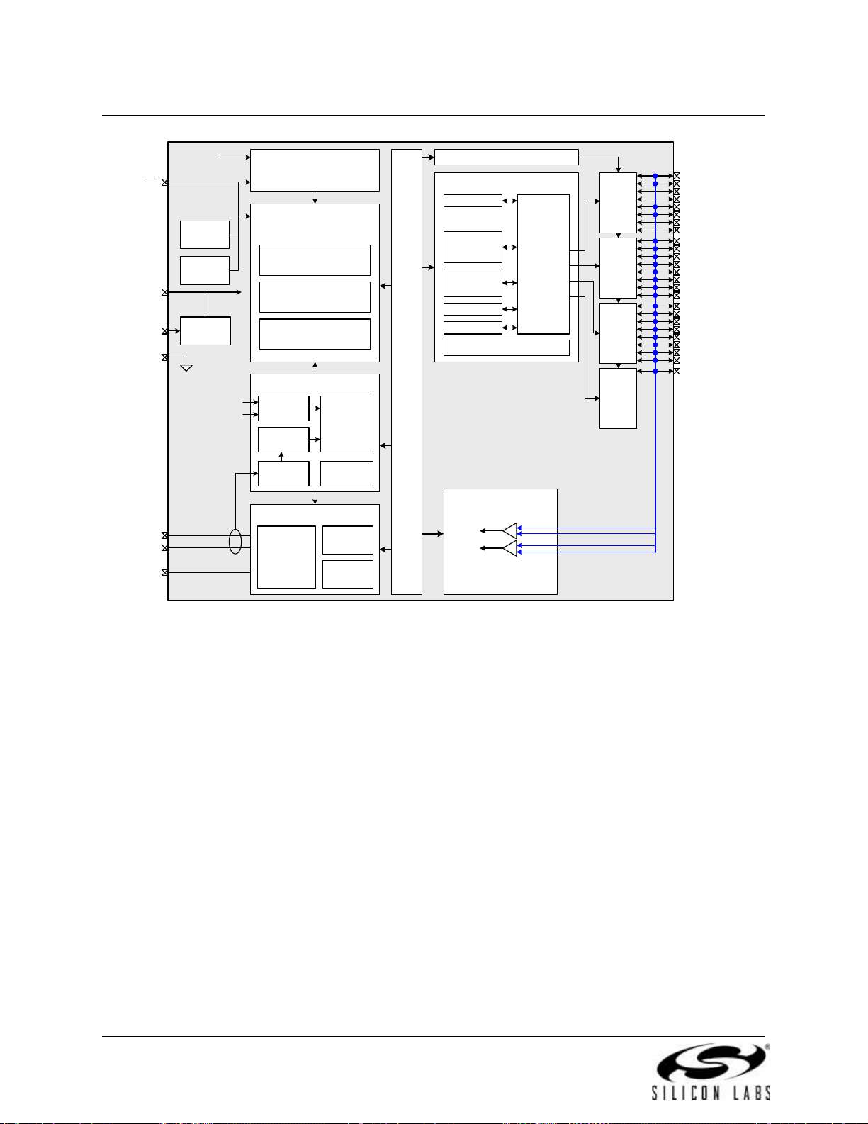
Analog Peripherals
10-bit
200ksps
ADC
A
M
U
X
Temp
Sensor
2 Comparators
+
-
VREFVDD
CP0
VDD
+
-
CP1
VREF
Debug / Programming
Hardware
Port 0
Drivers
P0.0
AIN0 - AIN19
Port I/O Configuration
Digital Peripherals
Priority
Crossbar
Decoder
Crossbar Control
Power-On
Reset
Power
Net
UART0
Timers 0, 1,
2, 3
PCA/WDT
SMBus
UART1
SPI
P0.1
P0.2
P0.3
P0.4
P0.5
P0.6/XTAL1
P0.7/XTAL2
Port 1
Drivers
Port 2
Drivers
Port 3
Drivers
Port 4
Drivers
P1.0
P1.1
P1.2
P1.3
P1.4/CNVSTR
P1.5/VREF
P1.6
P1.7
P2.0
P2.1
P2.2
P2.3
P2.4
P2.5
P2.6
P2.7
P3.0
P3.1
P3.2
P3.3
P3.4
P3.5
P3.6
P3.7
P4.0
P4.1
P4.2
P4.3
P4.4
P4.5
P4.6
P4.7
Supply
Monitor
System Clock Setup
External
Oscillator
Internal
Oscillator
XTAL1
XTAL2
Low Freq.
Oscillator
Clock
Multiplier
Clock
Recovery
USB Peripheral
Controller
1k Byte
RAM
Full / Low
Speed
Transceiver
External Memory
Interface
Control
Address
Data
P1
P2 / P3
P4
SFR
Bus
Voltage
Regulator
D+
D-
VBUS
VDD
VREG
GND
C2CK/RST
Reset
C2D
CIP-51 8051
Controller Core
64/32k Byte ISP FLASH
Program Memory
256 Byte RAM
4/2k Byte XRAM
Figure 1.1. C8051F340/1/4/5 Block Diagram
Rev. 1.3 19
Page 20
C8051F340/1/2/3/4/5/6/7/8/9/A/B/C/D
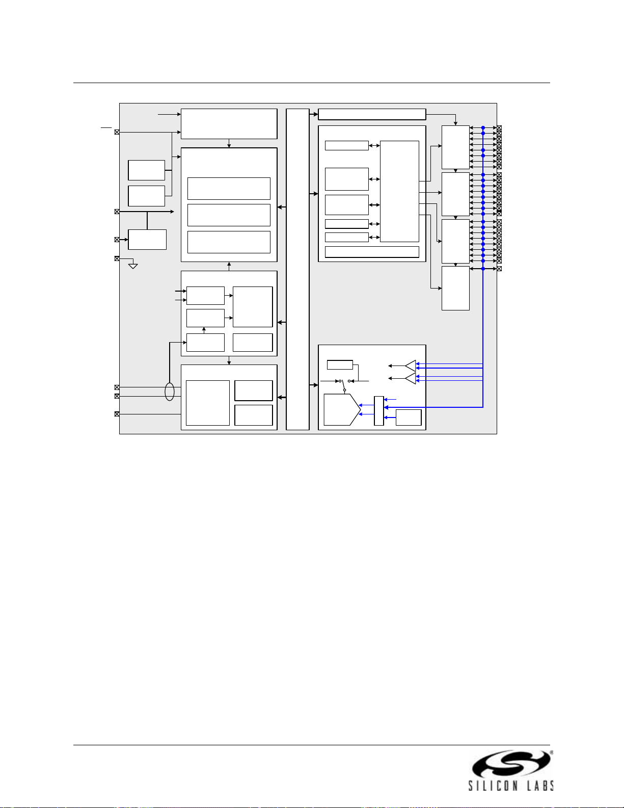
Analog Peripherals
10-bit
200 ksps
ADC
A
M
U
X
Temp
Sensor
2 Comparators
+
-
VREFVDD
CP0
VDD
+
-
CP1
VREF
Debug / Programming
Hardware
Port 0
Drivers
P0.0
AIN0 - AIN20
Port I/O Configuration
Digital Peripherals
Priority
Crossbar
Decoder
Crossbar Control
Power-On
Reset
Power
Net
UART0
Timers 0, 1,
2, 3
PCA/WDT
SMBus
SPI
P0.1
P0.2/XTAL1
P0.3/XTAL2
P0.4
P0.5
P0.6/CNVSTR
P0.7/VREF
Port 1
Drivers
Port 2
Drivers
Port 3
Drivers
P1.0
P1.1
P1.2
P1.3
P1.4
P1.5
P1.6
P1.7
P2.0
P2.1
P2.2
P2.3
P2.4
P2.5
P2.6
P2.7
P3.0/C2D
Supply
Monitor
System Clock Setup
External
Oscillator
Internal
Oscillator
XTAL1
XTAL2
Low Freq.
Oscillator*
Clock
Multiplier
Clock
Recovery
USB Peripheral
Controller
1 kB RAM
Full / Low
Speed
Transceiver
SFR
Bus
Voltage
Regulator
D+
D-
VBUS
VDD
VREG
GND
C2CK/RST
Reset
CIP-51 8051
Controller Core
64/32 kB ISP FLASH
Program Memory
256 Byte RAM
4/2 kB XRAM
C2D
*Low Frequency Oscillator option not available on C8051F346/7
20 Rev. 1.3
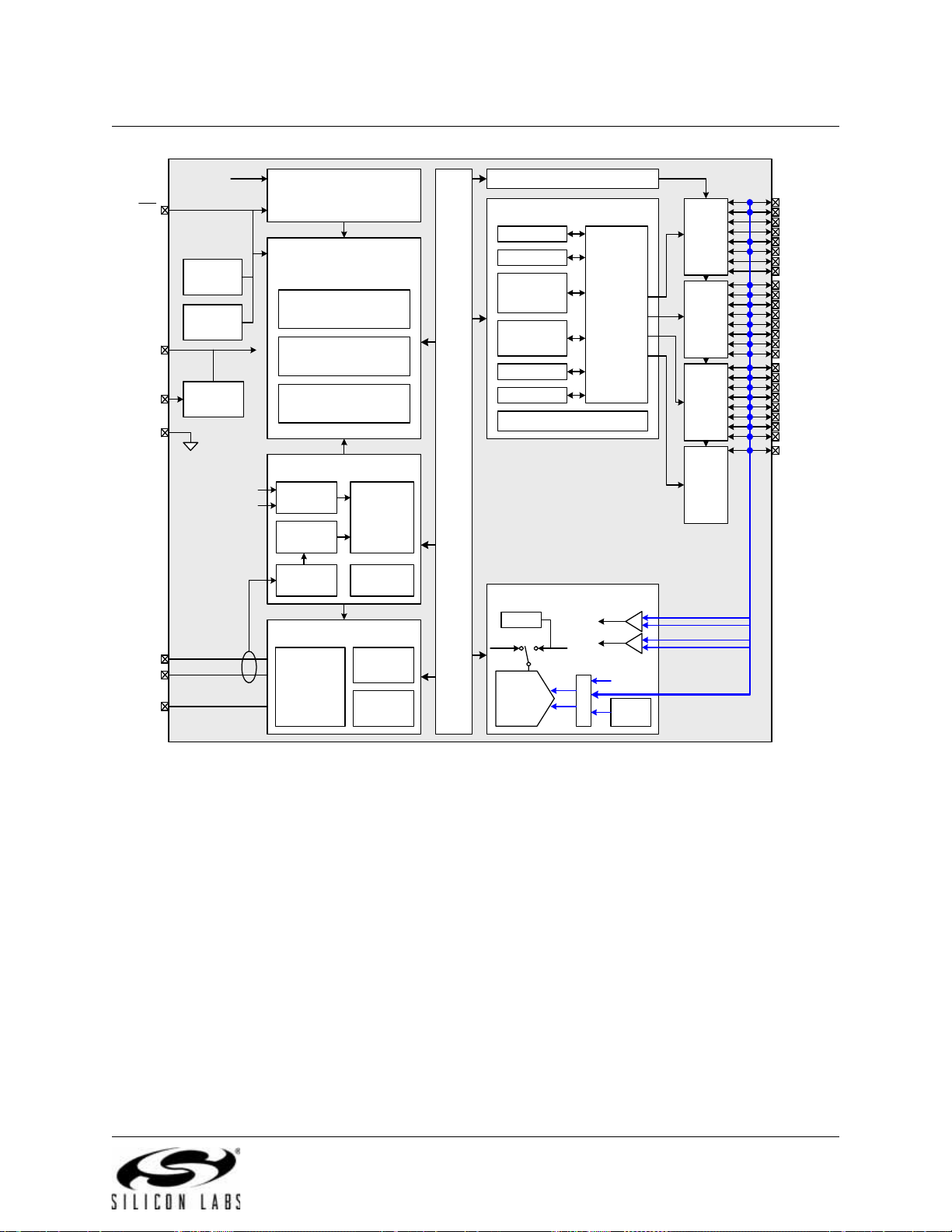
Figure 1.2. C8051F342/3/6/7 Block Diagram
Page 21
C8051F340/1/2/3/4/5/6/7/8/9/A/B/C/D
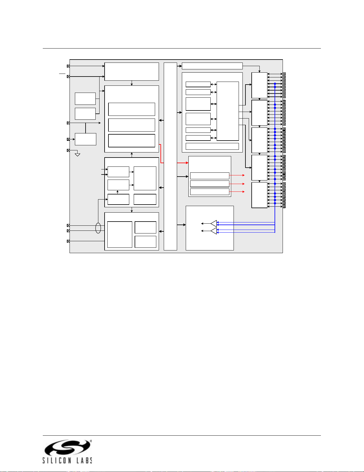
Debug / Programming
Hardware
Port 0
Drivers
P0.0
Port I/O Configuration
Digital Peripherals
Priority
Crossbar
Decoder
Crossbar Control
Power-On
Reset
Power
Net
UART0
Timers 0, 1,
2, 3
PCA/WDT
SMBus
UART1
SPI
P0.1
P0.2
P0.3
P0.4
P0.5
P0.6/XTAL1
P0.7/XTAL2
Port 1
Drivers
Port 2
Drivers
Port 3
Drivers
Port 4
Drivers
P1.0
P1.1
P1.2
P1.3
P1.4/CNVSTR
P1.5/VREF
P1.6
P1.7
P2.0
P2.1
P2.2
P2.3
P2.4
P2.5
P2.6
P2.7
P3.0
P3.1
P3.2
P3.3
P3.4
P3.5
P3.6
P3.7
P4.0
P4.1
P4.2
P4.3
P4.4
P4.5
P4.6
P4.7
Supply
Monitor
System Clock Setup
External
Oscillator
Internal
Oscillator
XTAL1
XTAL2
Low Freq.
Oscillator
Clock
Multiplier
Clock
Recovery
USB Peripheral
Controller
1k Byte
RAM
Full / Low
Speed
Transceiver
External Memory
Interface
Control
Address
Data
P1
P2 / P3
P4
Voltage
Regulator
D+
D-
VBUS
VDD
VREG
GND
C2CK/RST
Reset
C2D
CIP-51 8051
Controller Core
64/32 kB ISP FLASH
Program Memory
256 Byte RAM
4/2 kB XRAM
Analog Peripherals
2 Comparators
+
-
CP0
+
-
CP1
SFR
Bus
Figure 1.3. C8051F348/C Block Diagram
Rev. 1.3 21
Page 22
C8051F340/1/2/3/4/5/6/7/8/9/A/B/C/D
Debug / Programming
Hardware
Port 0
Drivers
P0.0
Port I/O Configuration
Digital Peripherals
Priority
Crossbar
Decoder
Crossbar Control
Power-On
Reset
Power
Net
UART0
Timers 0, 1,
2, 3
PCA/WDT
SMBus
SPI
P0.1
P0.2/XTAL1
P0.3/XTAL2
P0.4
P0.5
P0.6/CNVSTR
P0.7/VREF
Port 1
Drivers
Port 2
Drivers
Port 3
Drivers
P1.0
P1.1
P1.2
P1.3
P1.4
P1.5
P1.6
P1.7
P2.0
P2.1
P2.2
P2.3
P2.4
P2.5
P2.6
P2.7
P3.0/C2D
Supply
Monitor
System Clock Setup
External
Oscillator
Internal
Oscillator
XTAL1
XTAL2
Low Freq.
Oscillator
Clock
Multiplier
Clock
Recovery
USB Peripheral
Controller
1 kB RAM
Full / Low
Speed
Transceiver
SFR
Bus
Voltage
Regulator
D+
D-
VBUS
VDD
VREG
GND
C2CK/RST
Reset
CIP-51 8051
Controller Core
64/32 kB ISP FLASH
Program Memory
256 Byte RAM
4/2 kB XRAM
C2D
Analog Peripherals
2 Comparators
+
-
CP0
+
-
CP1
Figure 1.4. C8051F349/D Block Diagram
22 Rev. 1.3
Page 23
C8051F340/1/2/3/4/5/6/7/8/9/A/B/C/D
Analog Peripherals
10-bit
200 ksps
ADC
A
M
U
X
Temp
Sensor
2 Comparators
+
-
VREFVDD
CP0
VDD
+
-
CP1
VREF
Debug / Programming
Hardware
Port 0
Drivers
P0.0
AIN0 - AIN20
Port I/O Configuration
Digital Peripherals
Priority
Crossbar
Decoder
Crossbar Control
Power-On
Reset
Power
Net
UART0
Timers 0, 1,
2, 3
PCA/WDT
SMBus
SPI
P0.1
P0.2/XTAL1
P0.3/XTAL2
P0.4
P0.5
P0.6/CNVSTR
P0.7/VREF
Port 1
Drivers
Port 2
Drivers
Port 3
Drivers
P1.0
P1.1
P1.2
P1.3
P1.4
P1.5
P1.6
P1.7
P2.0
P2.1
P2.2
P2.3
P2.4
P2.5
P2.6
P2.7
P3.0/C2D
Supply
Monitor
System Clock Setup
External
Oscillator
Internal
Oscillator
XTAL1
XTAL2
Low Freq.
Oscillator*
Clock
Multip lier
Clock
Recovery
USB Peripheral
Controller
1 kB RAM
Full / Lo w
Speed
Transceiver
SFR
Bus
Voltage
Regulator
D+
D-
VBUS
VDD
VREG
GND
C2CK/RST
Reset
CIP-51 8051
Controller Core
64/32 k B IS P FLA SH
Program Memory
256 Byte RAM
4/2 kB XRAM
C2D
UART1
Figure 1.5. C8051F34A/B Block Diagram
Rev. 1.3 23
Page 24
C8051F340/1/2/3/4/5/6/7/8/9/A/B/C/D
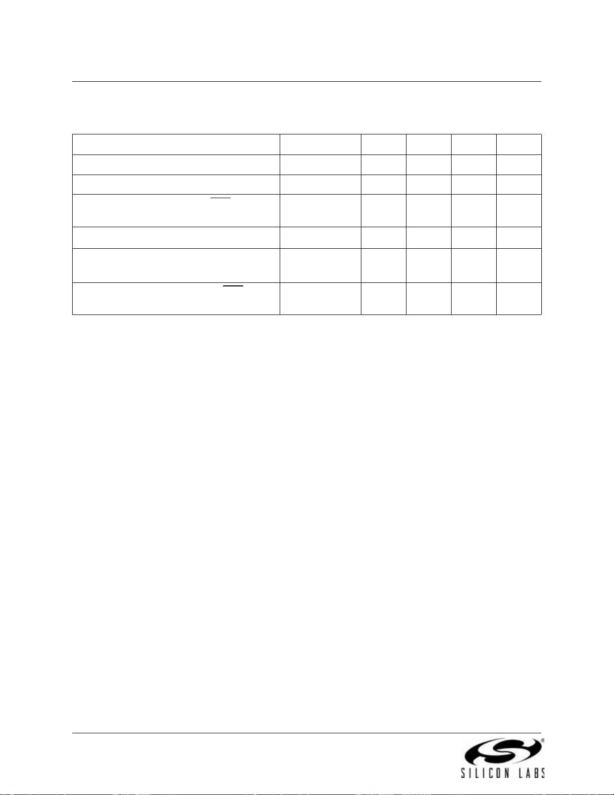
2. Absolute Maximum Ratings
Table 2.1. Absolute Maximum Ratings*
Parameter Conditions Min Typ Max Units
Ambient temperature under bias –55 125 °C
Storage Temperature –65 150 °C
Voltage on any Port I/O Pin or RST
respect to GND
Voltage on V
Maximum Total current through V
GND
Maximum output current sunk by RST
Port pin
*Note: Stresses above those listed under “Absolute Maximum Ratings” may cause permanent damage to the
device. This is a stress rating only and functional operation of the devices at those or any other conditions
above those indicated in the operation listings of this specification is not implied. Exposure to maximum rating
conditions for extended periods may affect device reliability.
with respect to GND –0.3 4.2 V
DD
DD
with
and
or any
–0.3 5.8 V
500 mA
100 mA
24 Rev. 1.3
Page 25
C8051F340/1/2/3/4/5/6/7/8/9/A/B/C/D
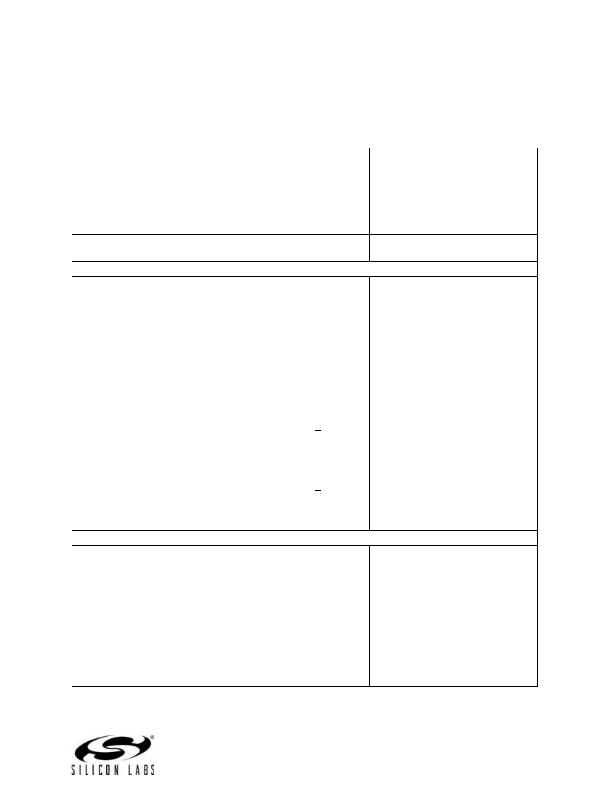
3. Global DC Electrical Characteristics
Table 3.1. Global DC Electrical Characteristics
–40 to +85 °C, 25 MHz System Clock unless otherwise specified.
Parameter Conditions Min Typ Max Units
Digital Supply Voltage
1
Digital Supply RAM Data
Retention Voltage
SYSCLK (System Clock)
2
C8051F340/1/2/3/A/B/C/D
C8051F344/5/6/7/8/9
Specified Operating
Temperature Range
Digital Supply Current - CPU Active (Normal Mode, accessing Flash)
I
DD
3
VDD = 3.3 V, SYSCLK = 48 MHz
= 3.3 V, SYSCLK = 24 MHz
V
DD
= 3.3 V, SYSCLK = 1 MHz
V
DD
= 3.3 V, SYSCLK = 80 kHz
V
DD
VRST 3.3 3.6 V
–40 +85 °C
1.5 V
0
0
25.9
13.9
0.69
55
48
25
.5
28
15.7
MHz
mA
mA
mA
µA
= 3.6 V, SYSCLK = 48 MHz
V
DD
= 3.6 V, SYSCLK = 24 MHz
V
DD
Supply Sensitivity
I
DD
3,4
SYSCLK = 1 MHz,
relative to V
= 3.3 V
DD
SYSCLK = 24 MHz,
= 3.3 V
DD
Frequency Sensitivity
I
DD
3,5
relative to V
VDD = 3.3 V, SYSCLK < 30 MHz,
T = 25 ºC
= 3.3 V, SYSCLK > 30 MHz,
V
DD
T = 25 ºC
= 3.6 V, SYSCLK < 30 MHz,
V
DD
T = 25 ºC
= 3.6 V, SYSCLK > 30 MHz,
V
DD
T = 25 ºC
Digital Supply Current - CPU Inactive (Idle Mode, not accessing Flash)
3
I
DD
Supply Sensitivity
I
DD
3,4
VDD = 3.3 V, SYSCLK = 48 MHz
= 3.3 V, SYSCLK = 24 MHz
V
DD
= 3.3 V, SYSCLK = 1 MHz
V
DD
= 3.3 V, SYSCLK = 80 kHz
V
DD
= 3.6 V, SYSCLK = 48 MHz
V
DD
= 3.6 V, SYSCLK = 24 MHz
V
DD
SYSCLK = 1 MHz,
relative to V
= 3.3 V
DD
SYSCLK = 24 MHz,
relative to V
= 3.3 V
DD
29.7
15.9
47
46
0.69
0.44
0.80
0.50
16.6
8.25
0.44
35
18.6
9.26
41
39
32.3
18
18
9.34
20.9
10.5
.75
mA
mA
%/V
%/V
MHz
mA/
mA/MHz
mA/MHz
mA/MHz
mA
mA
mA
µA
mA
mA
%/V
%/V
Rev. 1.3 25
Page 26
C8051F340/1/2/3/4/5/6/7/8/9/A/B/C/D
Table 3.1. Global DC Electrical Characteristics (Continued)
–40 to +85 °C, 25 MHz System Clock unless otherwise specified.
Parameter Conditions Min Typ Max Units
Frequency Sensitivity
I
DD
3,6
VDD = 3.3 V, SYSCLK < 1 MHz,
T = 25 ºC
= 3.3 V, SYSCLK > 1 MHz,
V
DD
T = 25 ºC
0.44
0.32
MHz
mA/
mA/MHz
= 3.6 V, SYSCLK < 1 MHz,
V
DD
0.49
mA/MHz
T = 25 ºC
= 3.6 V, SYSCLK > 1 MHz,
V
DD
0.36
mA/MHz
T = 25 ºC
Digital Supply Current (Stop
Mode, shutdown)
Digital Supply Current for USB
Module (USB Active Mode)
Digital Supply Current for USB
Module (USB Suspend Mode)
Notes:
1. USB Requires 3.0 V Minimum Supply Voltage.
2. SYSCLK must be at least 32 kHz to enable debugging.
3. Based on
4. Active and Inactive IDD at voltages and frequencies other than those specified can be calculated using the IDD
Supply Sensitivity. For example, if the VDD is 3.0 V instead of 3.3 V at 24 MHz: IDD = 13.9 mA typical at 3.3 V
and SYSCLK = 24 MHz. From this, I
= 24 MHz.
5. IDD can be estimated for frequencies < 30 MHz by multiplying the frequency of interest by the frequency
sensitivity number for that range. When using these numbers to estimate I
be the current at 24 MHz (or 48 MHz) minus the difference in current indicated by the frequency sensitivity
number. For example: VDD = 3.3 V; SYSCLK = 35 MHz, IDD = 13.9 mA – (24 MHz – 35 MHz) x 0.44 mA/MHz =
18.74 mA.
le IDD can be estimated for frequencies < 1 MHz by multiplying the frequency of interest by the frequency
6. Id
sensitivity number for that range. When using these numbers to estimate Idle IDD for > 1 MHz, the estimate
should be the current at 24 MHz (or 48 MHz) minus the difference in current indicated by the frequency
sensitivity number. For example: V
0.32 mA/MHz = 2.17 mA.
device characterization of data; Not production tested.
Oscillator not running,
monitor disabled
V
DD
= 3.3 V, USB Clock = 48 MHz
V
DD
= 3.6 V, USB Clock = 48 MHz
V
DD
Oscillator not running
monitor disabled
V
DD
= 13.9 mA + 0.46 x (3.0 V – 3.3 V) = 13.76 mA at 3.0 V and SYSCLK
DD
= 3.3 V; SYSCLK = 5 MHz, Idle IDD = 8.25 mA – (24 MHz – 5 MHz) x
DD
< 0.1 µA
8.69
9.59
< 0.1 µA
for > 30 MHz, the estimate should
DD
mA
mA
Other electrical characteristics tables are fo und in the data sheet section corresponding to the associated
peripherals. For more information on electrical characteristics for a specific peripheral, refer to the page
indicated in
26 Rev. 1.3
Table 3.2.
Page 27
C8051F340/1/2/3/4/5/6/7/8/9/A/B/C/D
Table 3.2. Index to Electrical Characteristics Tables
Table Title Page No.
ADC0 Electrical Characteristics 56
Voltage Reference Electrical Char
Comparator Electrical Characteristics 68
Voltage Regulator Electrical Specifications 69
Reset Electrical Characteristics 106
Flash Electrical Ch
AC Parameters for Exter
Oscillator Electrical Characteristics 141
Port I/O DC Electrical Characteristics 158
USB Transceiver Electrical Characteristics 187
aracteristics 109
nal Memory Interface 130
acteristics 58
Rev. 1.3 27
Page 28
C8051F340/1/2/3/4/5/6/7/8/9/A/B/C/D
4. Pinout and Package Definitions
Table 4.1. Pin Definitions for the C8051F340/1/2/3/4/5/6/7/8/9/A/B/C/D
Name
V
DD
GND 7 3 Ground.
RST/
C2CK
C2D 14 — D I/O Bi-directional data signal for the C2 Debug Interface.
P3.0 /
C2D
REGIN 11 7 Power In 5 V Regulator Input. This pin is the input to the on-chip volt-
VBUS 12 8 D In VBUS Sense Input. This pin should be connected to the
Pin Numbers
Type Description
48-pin 32-pin
10 6 Power In
Power
Out
13 9 D I/O
D I/O
— 10 D I/O
D I/O
2.7–3.6 V Power Supply Voltage Input.
3.3 V Voltage Regulator Output. See Section 8.
Device Reset. Open-drain output of internal POR or VDD
monitor. An external source can initiate a system reset by
driving this pin low for at least 15 µs. See Section 11.
Clock signal for the C2 Debug Interface.
Port 3.0. See Section 15 for a complete description of Port
3.
Bi-directional data signal for the C2 Debug Interface.
age regulator.
VBUS signal
cates a USB network connection.
of a USB network. A 5 V signal on this pin indi-
D+ 8 4 D I/O USB D+.
D- 9 5 D I/O USB D–.
P0.0 6 2 D I/O or
A In
P0.1 5 1 D I/O or
A In
P0.2 4 32 D I/O or
A In
P0.3 3 31 D I/O or
A In
P0.4 2 30 D I/O or
A In
P0.5 1 29 D I/O or
A In
P0.6 48 28 D I/O or
A In
P0.7 47 27 D I/O or
A In
Port 0.0. See Section 15 for a complete description of Port
0.
Port 0.1.
Port 0.2.
Port 0.3.
Port 0.4.
Port 0.5.
Port 0.6.
Port 0.7.
28 Rev. 1.3
Page 29
C8051F340/1/2/3/4/5/6/7/8/9/A/B/C/D
Table 4.1. Pin Definitions for the C8051F340/1/2/3/4/5/6/7/8/9/A/B/C/D (Continued)
Name
P1.0 46 26 D I/O or
P1.1 45 25 D I/O or
P1.2 44 24 D I/O or
P1.3 43 23 D I/O or
P1.4 42 22 D I/O or
P1.5 41 21 D I/O or
P1.6 40 20 D I/O or
P1.7 39 19 D I/O or
P2.0 38 18 D I/O or
P2.1 37 17 D I/O or
Pin Numbers
Type Description
48-pin 32-pin
A In
A In
A In
A In
A In
A In
A In
A In
A In
A In
Port 1.0. See Section 15 for a complete description of Port
1.
Port 1.1.
Port 1.2.
Port 1.3.
Port 1.4.
Port 1.5.
Port 1.6.
Port 1.7.
Port 2.0. See Section 15 for a complete description of Port
2.
Port 2.1.
P2.2 36 16 D I/O or
A In
P2.3 35 15 D I/O or
A In
P2.4 34 14 D I/O or
A In
P2.5 33 13 D I/O or
A In
P2.6 32 12 D I/O or
A In
P2.7 31 11 D I/O or
A In
P3.0 30 — D I/O or
A In
P3.1 29 — D I/O or
A In
P3.2 28 — D I/O or
A In
Port 2.2.
Port 2.3.
Port 2.4.
Port 2.5.
Port 2.6.
Port 2.7.
Port 3.0. See Section 15 for a complete description of Port
3.
Port 3.1.
Port 3.2.
Rev. 1.3 29
Page 30
C8051F340/1/2/3/4/5/6/7/8/9/A/B/C/D
Table 4.1. Pin Definitions for the C8051F340/1/2/3/4/5/6/7/8/9/A/B/C/D (Continued)
Name
P3.3 27 — D I/O or
P3.4 26 — D I/O or
P3.5 25 — D I/O or
P3.6 24 — D I/O or
P3.7 23 — D I/O or
P4.0 22 — D I/O or
P4.1 21 — D I/O or
P4.2 20 — D I/O or
P4.3 19 — D I/O or
P4.4 18 — D I/O or
Pin Numbers
Type Description
48-pin 32-pin
A In
A In
A In
A In
A In
A In
A In
A In
A In
A In
Port 3.3.
Port 3.4.
Port 3.5.
Port 3.6.
Port 3.7.
Port 4.0. See Section 15 for a complete description of Port
4.
Port 4.1.
Port 4.2.
Port 4.3.
Port 4.4.
P4.5 17 — D I/O or
A In
P4.6 16 — D I/O or
A In
P4.7 15 — D I/O or
A In
Port 4.5.
Port 4.6.
Port 4.7.
30 Rev. 1.3
Page 31

C8051F340/1/2/3/4/5/6/7/8/9/A/B/C/D
1
2
3
4
5
6
7
8
9
10
11
12
36
35
34
33
32
31
30
29
28
27
26
25
48
47
46
45
44
43
42
41
40
39
38
37
VBUS
P2.2
P2.0
P1.7
P1.6
P1.2
P2.4
P2.3
P3.5
P3.4
P3.2
P3.1
P2.1
P0.6
P3.3
P0.7
P0.2
D-
REGIN
P0.3
P3.0
P1.4
P1.5
P0.5
P1.1
P1.0
P0.4
P1.3
13
14
15
16
17
18
19
20
21
22
23
24
P2.6
P2.5
C8051F340/1/4/5/8/C-GQ
Top View
GND
D+
P0.1
P0.0
VDD
P2.7
P3.6
P4.1
P4.0
P3.7
P4.2
P4.5
P4.4
P4.3
P4.6
RST / C2CK
C2D
P4.7
Figure 4.1. TQFP-48 Pinout Diagram (Top View)
Rev. 1.3 31
Page 32
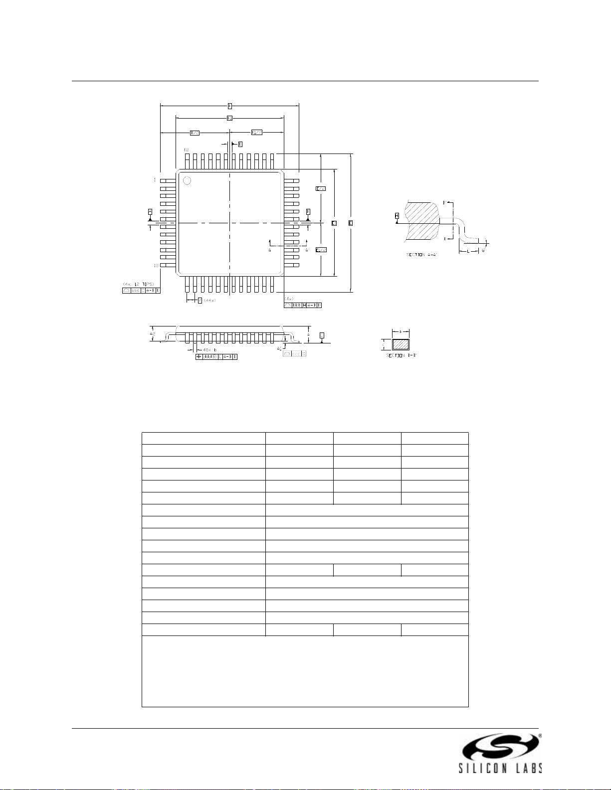
C8051F340/1/2/3/4/5/6/7/8/9/A/B/C/D
Figure 4.2. TQFP-48 Package Diagram
Table 4.2. TQFP-48 Package Dimensions
Dimension Min Nom Max
A——1.20
A1 0.05 — 0.15
A2 0.95 1.00 1.05
b 0.170.220.27
c 0.09 — 0.20
D9.00 BSC
D1 7.00 BSC
e0.50 BSC
E9.00 BSC
E1 7.00 BSC
L 0.450.600.75
aaa 0.20
bbb 0.20
ccc 0.08
ddd 0.08
0° 3.5° 7°
Notes:
1. All dimen
2. Dimensi
3. Thi
4. The
specification for Small Body Components.
sions shown are in millimeters (mm) unless otherwise noted.
oning and Tolerancing per ANSI Y14.5M-1994.
s drawing conforms to JEDEC outline MS-026, variation ABC.
recommended card reflow profile is per the JEDEC/IPC J-STD-020
32 Rev. 1.3
Page 33
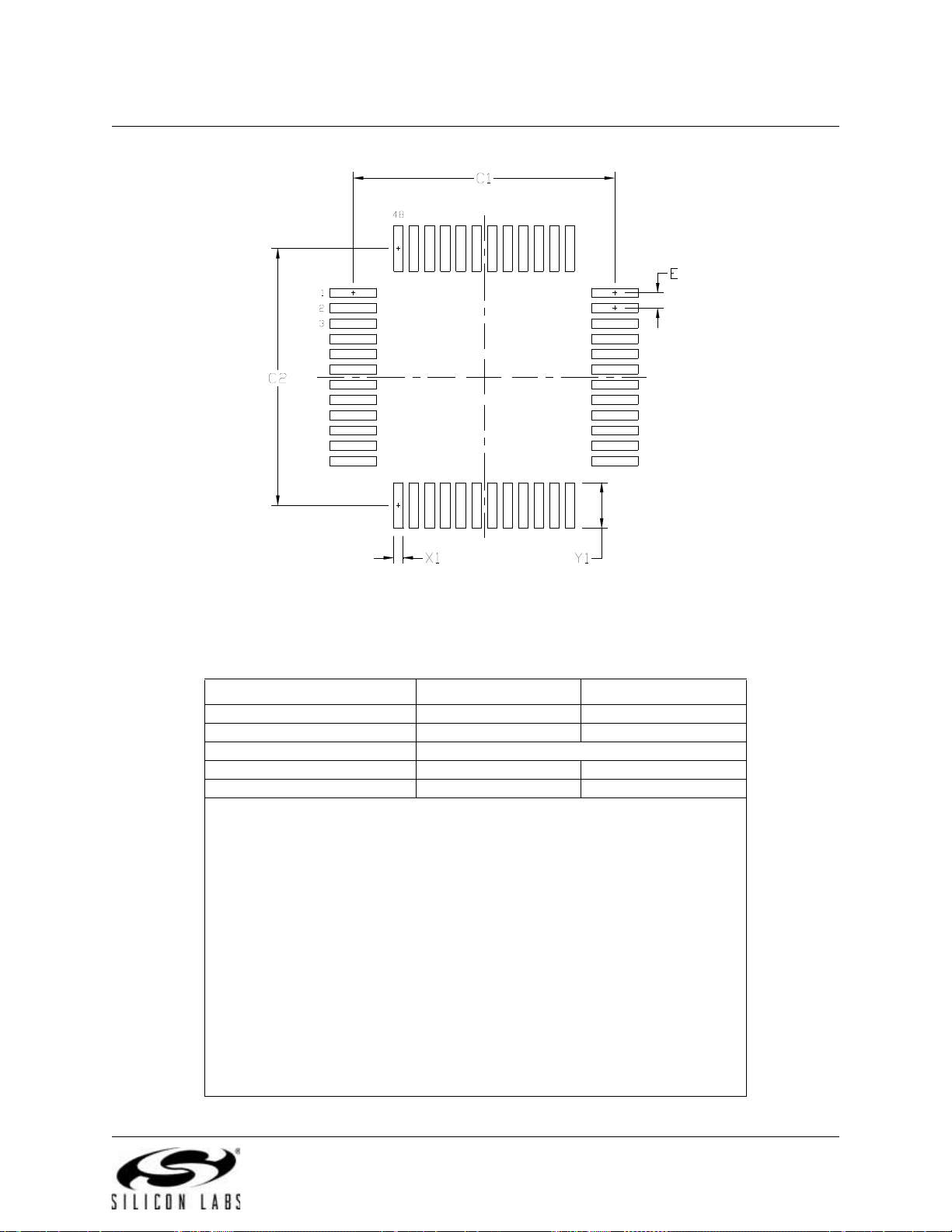
C8051F340/1/2/3/4/5/6/7/8/9/A/B/C/D
Figure 4.3. TQFP-48 Recommended PCB Land Pattern
Table 4.3. TQFP-48 PCB Land Pattern Dimensions
Dimension Min Max
C1 8.30 8.40
C
2 8.30 8.40
E 0.50 BSC
X1 0.20 0.30
Y1 1.40 1.50
Notes:
General:
1. All dimensions shown
his Land Pattern Design is based on the IPC-7351 guidelines.
2. T
Solder Mask Design:
3. All metal pads are to be non-solder mask defined (NSMD). Clearance between
the solder mask and the metal pad is to be 60 µm minimum, all the way around
the pad.
Stencil Design:
ainless steel, laser-cut and electro-polished stencil with trapezoidal walls
4. A st
should be used to assure good solder paste release.
5. The stencil thickness should be 0.125 mm (5 mils).
he ratio of stencil aperture to land pad size should be 1:1 for all pads.
6. T
Card Assembly:
7. A No-Cle
8. T
he recommended card reflow profile is per the JEDEC/IPC J-STD-020
specification for Small Body Components.
an, Type-3 solder paste is recommended.
are in millimeters (mm) unless otherwise noted.
Rev. 1.3 33
Page 34
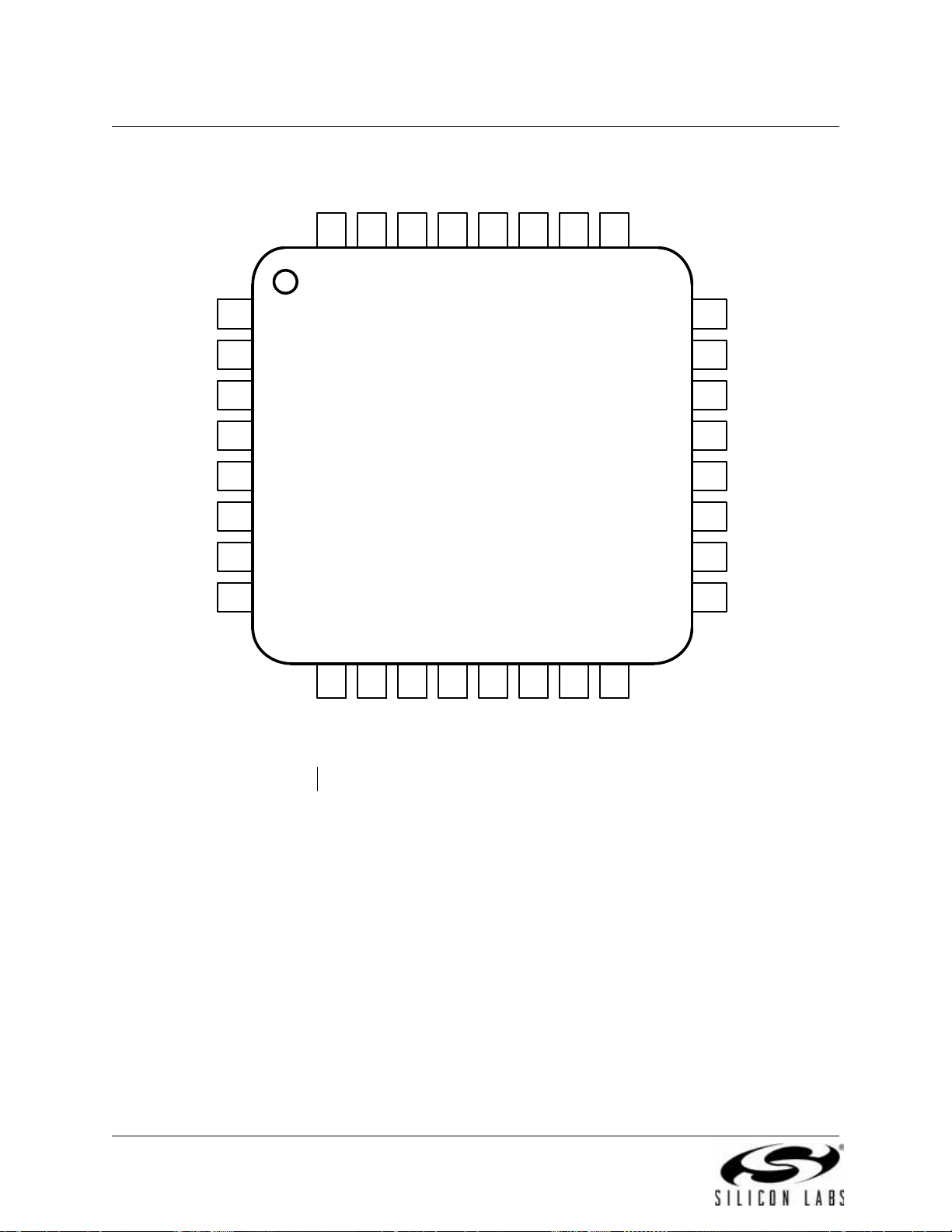
C8051F340/1/2/3/4/5/6/7/8/9/A/B/C/D
1
VBUS
P1.2
P1.7
P1.4
P1.3
P1.5D+
D-
GND
P0.1
P0.0
P2.0
P2.1
2
3
4
5
6
7
8
24
23
22
21
20
19
18
17
9
10
11
12
13
14
15
16
32
31
30
29
28
27
26
25
P1.6
C8051F342/3/6/7/9/A/B/D-GQ
Top View
VDD
REGIN
RST / C2CK
P3.0 / C2D
P2.7
P2.6
P2.5
P2.4
P2.3
P2.2
P1.1
P1.0
P0.7
P0.6
P0.5
P0.4
P0.3
P0.2
Figure 4.4. LQFP-32 Pinout Diagram (Top View)
34 Rev. 1.3
Page 35
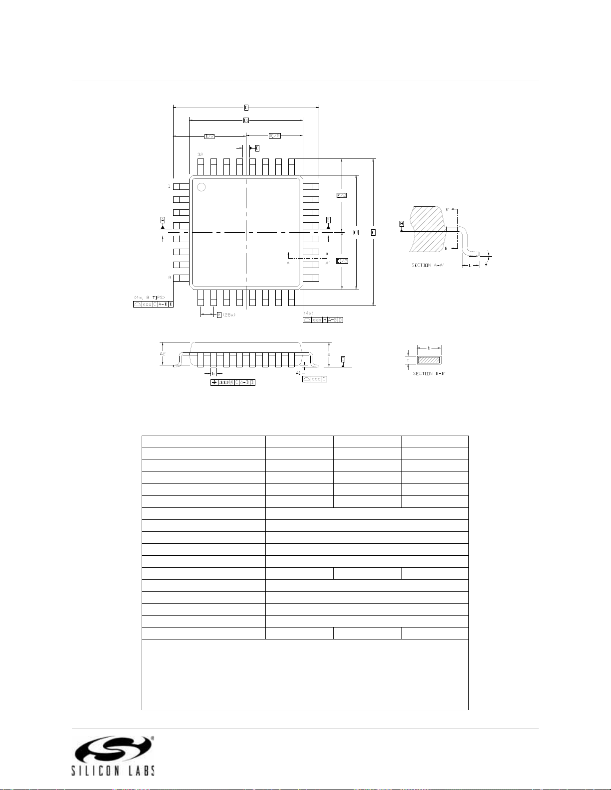
C8051F340/1/2/3/4/5/6/7/8/9/A/B/C/D
Figure 4.5. LQFP-32 Package Diagram
Table 4.4. LQFP-32 Package Dimensions
Dimension Min Nom Max
A——1.60
A1 0.05 — 0.15
A2 1.35 1.40 1.45
b 0.300.370.45
Notes:
1. All dimen
2. Dimensioning and Tolerancing per ANSI Y14.5M-1994.
3. Thi
4. The
c 0.09 — 0.20
D9.00 BSC
D1 7.00 BSC
e0.80 BSC
E9.00 BSC
E1 7.00 BSC
L 0.450.600.75
aaa 0.20
bbb 0.20
ccc 0.10
ddd 0.20
0° 3.5° 7°
sions shown are in millimeters (mm) unless otherwise noted.
s drawing conforms to JEDEC outline MS-026, variation BBA.
recommended card reflow profile is per the JEDEC/IPC J-STD-020
specification for Small Body Components.
Rev. 1.3 35
Page 36
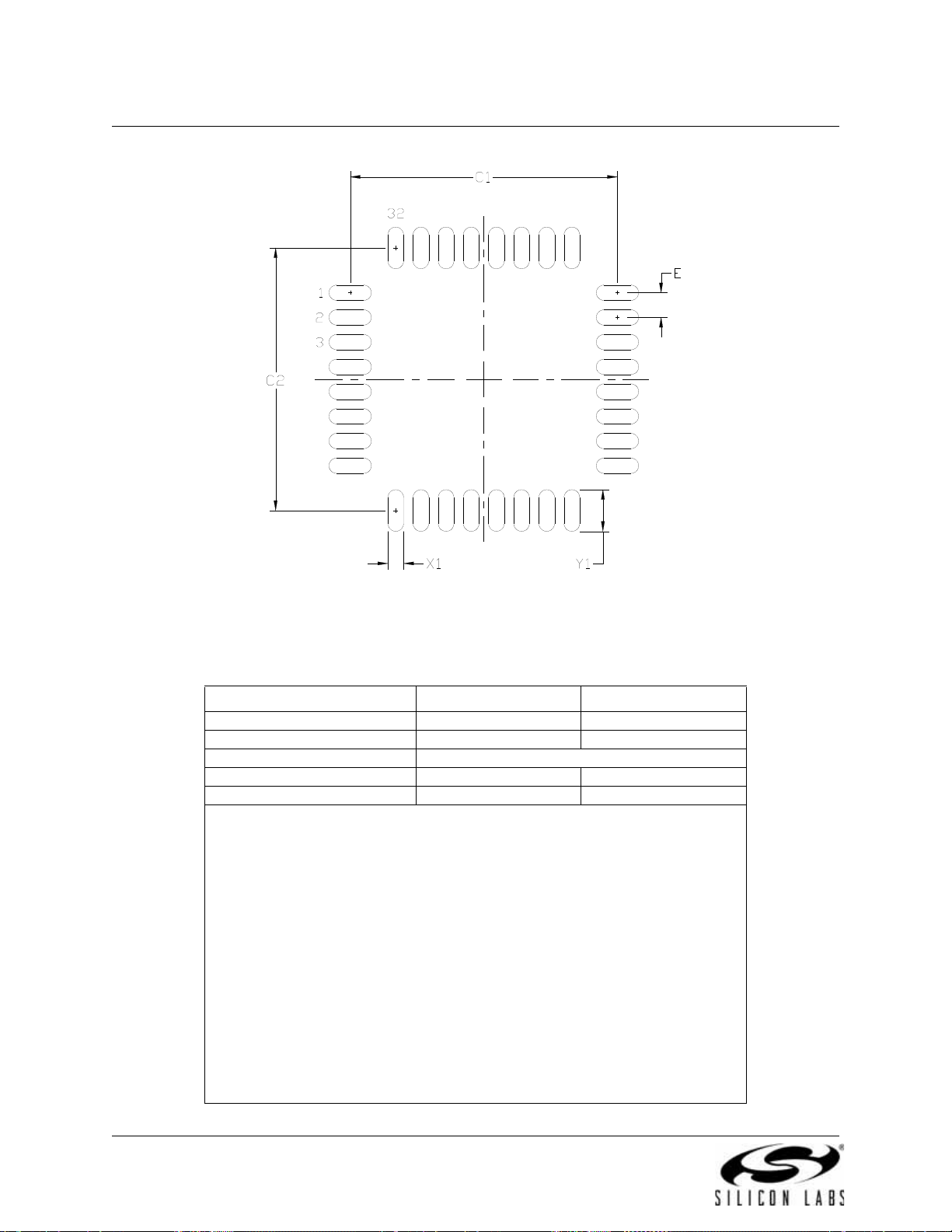
C8051F340/1/2/3/4/5/6/7/8/9/A/B/C/D
Figure 4.6. LQFP-32 Recommended PCB Land Pattern
Table 4.5. LQFP-32 PCB Land Pattern Dimensions
Dimension Min Max
C1 8.40 8.50
C
2 8.40 8.50
E 0.80 BSC
X1 0.40 0.50
Y1 1.25 1.35
Notes:
General:
1. All dimensions shown
his Land Pattern Design is based on the IPC-7351 guidelines.
2. T
Solder Mask Design:
3. All metal pads are to be non-solder mask defined (NSMD). Clearance between
the solder mask and the metal pad is to be 60 µm minimum, all the way around
the pad.
Stencil Design:
ainless steel, laser-cut and electro-polished stencil with trapezoidal walls
4. A st
should be used to assure good solder paste release.
5. The stencil thickness should be 0.125 mm (5 mils).
he ratio of stencil aperture to land pad size should be 1:1 for all pads.
6. T
Card Assembly:
7. A No-Cle
8. T
he recommended card reflow profile is per the JEDEC/IPC J-STD-020
specification for Small Body Components.
an, Type-3 solder paste is recommended.
are in millimeters (mm) unless otherwise noted.
36 Rev. 1.3
Page 37
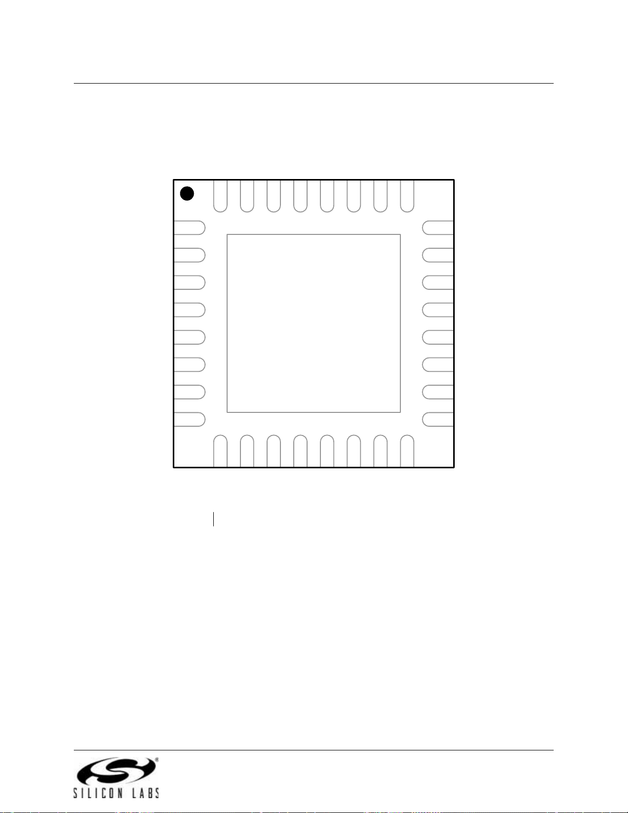
C8051F340/1/2/3/4/5/6/7/8/9/A/B/C/D
25 P1.1
17 P2.1
16P2.2
8VBUS
32
31
30
29
28
27
26
1
2
3
4
5
6
7
9
10
11
12
13
14
15
24
23
22
21
20
19
18
GND (optional)
C8051F342/3/6/7/9/A/B-GM
Top View
P1.0
P0.7
P0.6
P0.5
P0.4
P0.3
P0.2
P0.1
P0.0
GND
D+
D-
VDD
REGIN
RST / C2CK
P3.0 / C2D
P2.7
P2.6
P2.5
P2.4
P2.3
P2.0
P1.7
P1.6
P1.5
P1.4
P1.3
P1.2
Figure 4.7. QFN-32 Pinout Diagram (Top View)
Rev. 1.3 37
Page 38
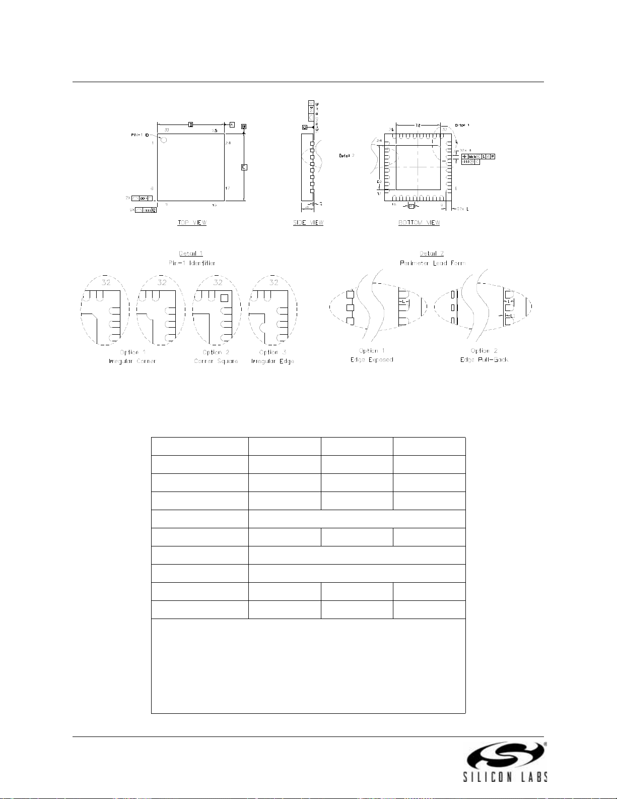
C8051F340/1/2/3/4/5/6/7/8/9/A/B/C/D
Figure 4.8. QFN-32 Package Drawing
Table 4.6. QFN-32 Package Dimensions
Dimension Min Nom Max
A 0.80 0.9 1.00
A1 0.00 0.02 0.05
b 0.18 0.25 0.30
D 5.00 BSC
D2 3.20 3.30 3.40
e 0.50 BSC
E 5.00 BSC
E2 3.20 3.30 3.40
L 0.30 0.40 0.50
Notes:
1. All dimensions shown
mensioning and T o lerancing per ANSI Y14.5M-1994.
2. Di
3. This drawing conforms to the JEDEC Solid State Outline MO-220,
variation VHHD except for custom features D2, E2, and L which are
toleranced per supplier designation.
commended card reflow profile is per the JEDEC/IPC J-STD-020
4. Re
specification for Small Body Components.
are in millimeters (mm) unless otherwise noted.
38 Rev. 1.3
Page 39
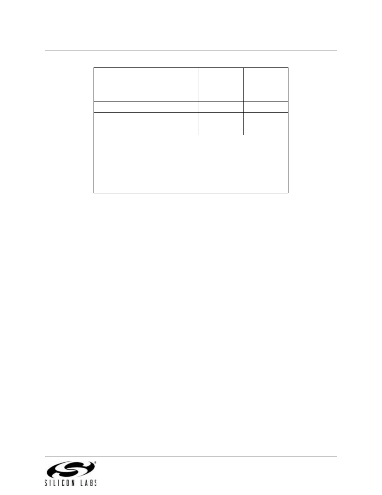
C8051F340/1/2/3/4/5/6/7/8/9/A/B/C/D
Table 4.6. QFN-32 Package Dimensions (Continued)
Dimension Min Nom Max
L1 0.00 — 0.15
aaa — — 0.15
bb
b — — 0.10
ddd — — 0.05
eee — — 0.08
Notes:
1. All dimensions shown are in millimeters (mm) unless otherwise noted.
2. Dimensioning and Tolerancing per ANSI Y14.5M-1994.
3. This drawing conforms to the JEDEC Solid State Outline MO-220,
variation VHHD except for custom features D2, E2, and L which are
toleranced per supplier designation.
4. Recommended card reflow profile is per the JEDEC/IPC J-STD-020
specification for Small Body Components.
Rev. 1.3 39
Page 40
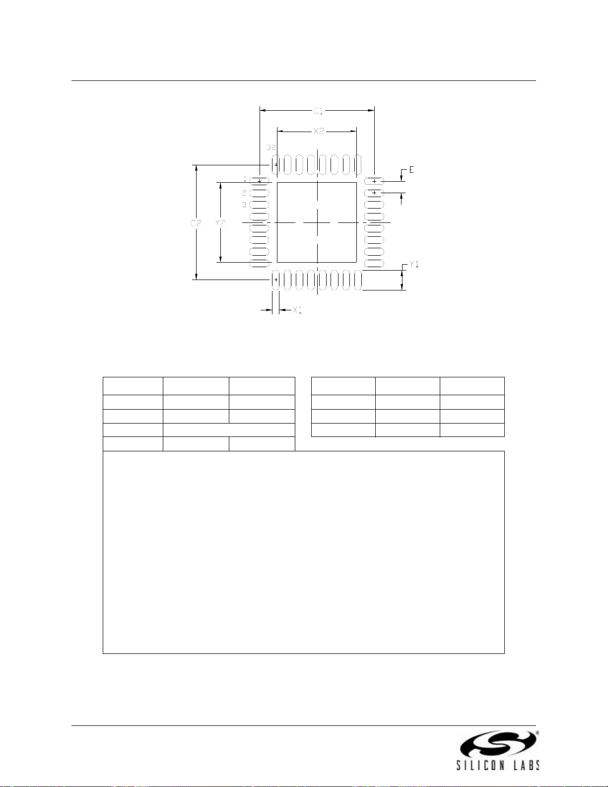
C8051F340/1/2/3/4/5/6/7/8/9/A/B/C/D
Figure 4.9. QFN-32 Recommended PCB Land Pattern
Table 4.7. QFN-32 PCB Land Pattern Dimesions
Dimension Min Max Dimension Min Max
C1 4.80 4.90 X2 3.20 3.40
C2 4.80 4.90 Y1 0.75 0.85
E 0.50 BSC Y2 3.20 3.40
X1 0.20 0.30
Notes:
General:
l dimensions shown are in millimeters (mm) unless otherwise noted.
1. Al
his Land Pattern Design is based on the IPC-7351 guidelines.
2. T
Solder Mask Design:
l metal pads are to be non-solder mask defined (NSMD). Clearance between the solder
3. Al
mask and the metal pad is to be 60m minimum, all the way around the pad.
Stencil Design:
4. A st
5. Th
6. T
7. A
Card Assembly:
8. A No-Cl
9. T
ainless steel, laser-cut and electro-polished stencil with trapezoidal walls should be used
to assure good solder paste release.
e stencil thickness should be 0.125 mm (5 mils).
he ratio of stencil aperture to land pad size should be 1:1 for all perimeter pins.
3x3 array of 1.0 mm openings on a 1.2mm pitch should be used for the center pad to assure
the proper paste volume.
ean, Type-3 solder paste is recommended.
he recommended card reflow profile is per the JEDEC/IPC J-STD-020 specification for Small
Body Components.
40 Rev. 1.3
Page 41
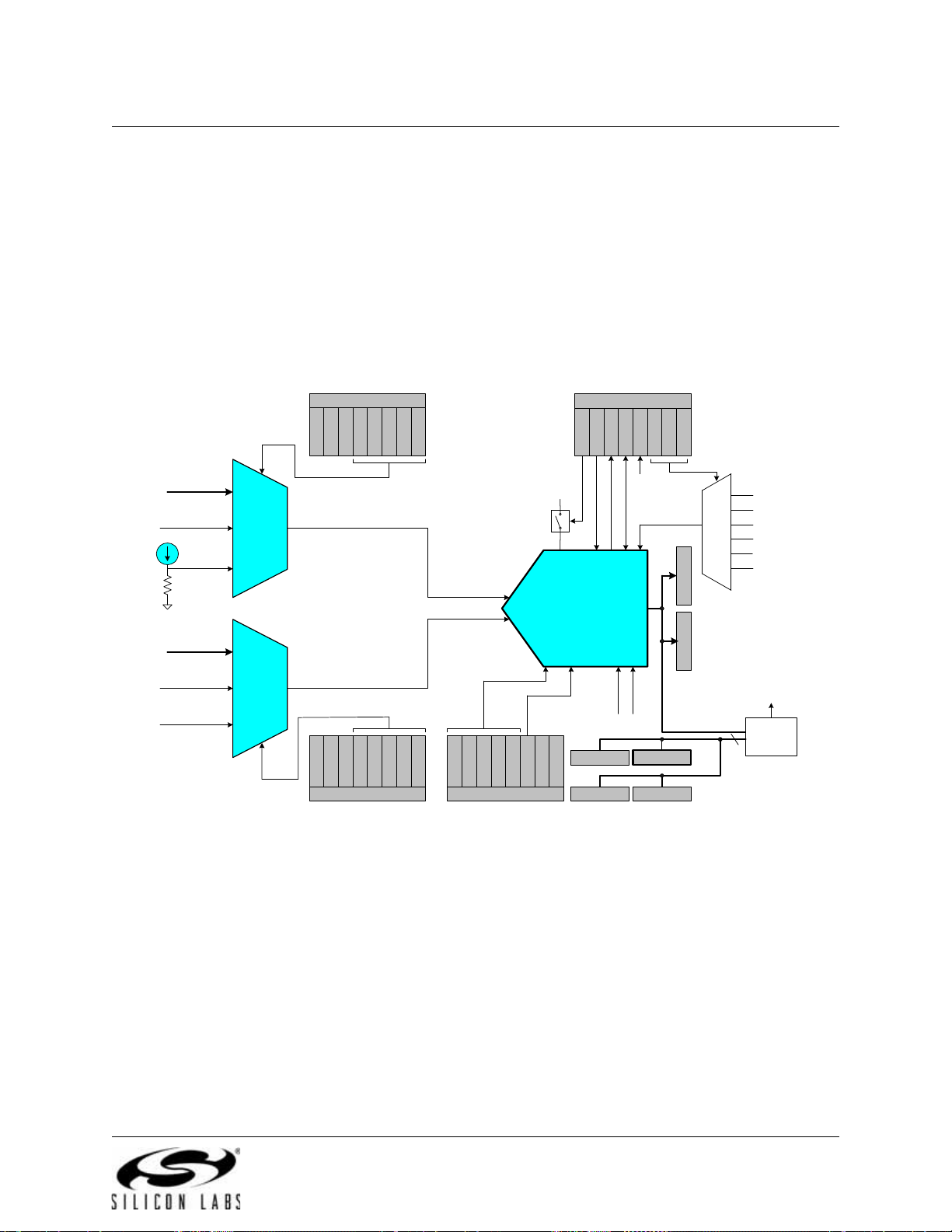
C8051F340/1/2/3/4/5/6/7/8/9/A/B/C/D
ADC0CF
AD0LJST
AD0SC0
AD0SC1
AD0SC2
AD0SC3
AD0SC4
10-Bit
SAR
ADC
REF
SYSCLK
ADC0H
32
ADC0CN
AD0CM0
AD0CM1
AD0CM2
AD0WINT
AD0BUSY
AD0INT
AD0TM
AD0EN
Timer 0 Overflow
Timer 2 Overflow
Timer 1 Overflow
Start
Conversion
000 AD0BUSY (W)
VDD
ADC0LTH
AD0WINT
001
010
011
100
CNVSTR Input
Window
Compare
Logic
GND
101 Timer 3 Overflow
ADC0LTL
ADC0GTH ADC0GTL
ADC0L
AMX0P
AMX0P4
AMX0P3
AMX0P2
AMX0P1
AMX0P0
AMX0N
AMX0N4
AMX0N3
AMX0N2
AMX0N1
AMX0N0
AIN+
AIN-
VREF
Positive
Input
(AIN+)
AMUX
VDD
Negative
Input
(AIN-)
AMUX
Temp
Sensor
Port I/O
Pins*
Port I/O
Pins*
* 21 Selections on 32-pin package
20 Selections on 48-pin package
5. 10-Bit ADC (ADC0, C8051F340/1/2/3/4/5/6/7/A/B Only)
The ADC0 subsystem for the C8051F34x devices consists of two analog multiplexers (referred to collectively as AMUX0), and a 200 ksps, 10-bit successive-approximation-register ADC with integrated
ck-and-hold and programmable window detector. The AMUX0, data conversion modes, and window
tra
detector are all configured und er software control via the Special Function Regi sters shown in Figure 5.1.
ADC0 operates in both Single-ended and Differential modes, and may be configured to measure voltages
t port pins, the Temperature Sensor output, or V
a
tion options for AMUX0 are detailed in SFR Definition 5.1 and SFR Definition 5.2. The ADC0 subsystem is
enabled only when the AD0EN bit in the ADC0 Control register (ADC0CN
system is in low power shutdown when
this bit is logic 0.
with respect to a port pin, VREF, or GND. The connec-
DD
) is set to logic 1. The ADC0 sub-
Figure 5.1. ADC0 Functional Block Diagram
Rev. 1.3 41
Page 42

C8051F340/1/2/3/4/5/6/7/8/9/A/B/C/D
5.1. Analog Multiplexer
AMUX0 selects the positive and negative inputs to the ADC. The positive input (AIN+) can be conn ected to
individual Port pins, the on-chip temperature sensor, or the positive power supply (V
input (AIN-) can be connected to individual Port pins, VREF, or GND. When GND is selected as the neg-
ative input, ADC0 operates in Single-ended Mode; at all other times, ADC0 operates in Differential
Mo
de. The ADC0 input channels are selected in the AMX0P and AMX0N registers as described in SFR
Definition 5.1 and SFR Definition 5.2.
). The negative
DD
The conversion code format differs between Single-en
and ADC0L contain the high and low bytes of the output conversion code from the ADC at the completion
of each conversion. Data can be right-justified or left- justified , depending o n the setting of the AD0 LJST bit
(ADC0CN.0). When in Single-ended Mode, conversion codes are represented as 10- bit unsigned integers.
Inputs are measured from ‘0’ to VREF x 1023/1024. Example codes are shown below for both right-justified and left-justified data. Unused bits in the ADC0H and ADC0L registers are set to ‘0’.
Input Voltage
Single-Ended)
(
VREF x 1023/1024 0x03FF 0xFFC0
VREF x 512/1024 0x0200 0x8000
VREF x 256/1024 0x0100 0x4000
0 0x0000 0x0000
When in Differential Mode, conversion codes are represented as 10-bit signed 2’s complement numbers.
uts are measured from –VREF to VREF x 511/512. Example codes are shown below for both right-jus-
Inp
tified and left-justified data. For right-justified data, the
data word. For left-justified data, the unused LSBs in the ADC0L regi ster are set to ‘0’.
Input Voltage
(Differential)
VREF x 511/512 0x01FF 0x7FC0
VREF x 256/512 0x0100 0x4000
0 0x0000 0x0000
–VREF x 256/512 0xFF00 0xC000
–VREF 0xFE00 0x8000
Right-Justified ADC0H:ADC0L
(AD0LJST = 0)
Right-Justified ADC0H:ADC0L
(AD0LJST = 0)
ded and Differential modes. The registers ADC0H
Left-Justified ADC0H:ADC0L
(AD0LJST = 1)
unused MSBs of ADC0H are a sign-extension of the
Left-Justified ADC0H:ADC0L
(AD0LJST = 1)
Important Note About ADC0 Input Configuration: Por
ured as analog inputs, and should be skipped by the Dig
input, set to ‘0’ the corresponding bit in register PnMDIN (for n = 0,1,2,3). To force the Crossbar to skip a
Port pin, set to ‘1’ the corresponding bit in register PnSKIP (for n = 0,1,2). See Section “15. Port Input/
Output” on page 142 for more Port I/O co
42 Rev. 1.3
nfiguration details.
t pins selected as ADC0 inputs should be config-
ital Crossbar. To configure a Port pin for analog
Page 43

C8051F340/1/2/3/4/5/6/7/8/9/A/B/C/D
Temperature
Voltage
V
TEMP
= (Gain x TempC) + Offset
Offset (V at 0 Celsius)
Gain (V / deg C)
Temp
C
= (V
TEMP
- Offset) / Gain
5.2. Temperature Sensor
The temperature sensor transfer function is shown in Figure 5.2. The outp ut volt age (V
ADC input when the temperature sensor is selected by bits AMX0P4-0 in register AMX0P. Values for the
fset and Slope parameters can be found in Table 5.1.
Of
) is the positive
TEMP
Figure 5.2. Temperature Sensor Transfer Function
The uncalibrated temperature sensor output is extreme
surements (see Table 5.1 for linearity specifications). For absolute tem
or gain calibration is recommended. Typically a 1-point (of
Step 1. Control/measure the ambient temperatur
Step 2. Power the device, and delay for a few seconds to allow for self-heating.
Step 3. Perform an ADC conversion with the temperature sensor selected as the positive input
and GND selected as the negative input.
Step 4. Calculate the o ffset characteristics, and store this value in non-volatile memory for use
with subsequent temperature sensor measurements.
Figure 5.3 shows the typical temperature sensor error
parameters which affect ADC measurement, in particular the voltage reference value, will also
ffect temperature measurement.
a
ly linear and suitable for relative temperature mea-
perature measurements, offset and/
fset) calibration includes the following steps:
e (this temperature must be known).
assuming a 1-point calibration at 25 °C. Note that
Rev. 1.3 43
Page 44

C8051F340/1/2/3/4/5/6/7/8/9/A/B/C/D
-40.00 -20.00
0.0
0
20.0
0
40.0
0
60.0
0
80.0
0
Temperature (degrees C)
Error (degrees C)
-5.00
-4.00
-3.00
-2.00
-1.00
0.0
0
1.0
0
2.0
0
3.0
0
4.0
0
5.0
0
-5.00
-4.00
-3.00
-2.00
-1.00
0.0
0
1.0
0
2.0
0
3.0
0
4.0
0
5.0
0
Figure 5.3. Temperature Sensor Error with 1-Point Calibration (VREF = 2.40 V)
44 Rev. 1.3
Page 45

C8051F340/1/2/3/4/5/6/7/8/9/A/B/C/D
5.3. Modes of Operation
ADC0 has a maximum conversion speed of 200 ksps. The ADC0 conversion clock is a divided version of
the system clock, determined by the AD0SC bits in the ADC0CF register (system clock divided by
(AD0SC + 1) for 0 AD0SC 31).
5.3.1. Starting a Conversion
A conversion can be initiated in one of five way s, depending on the programmed states of the ADC0 Start
of Conversion Mode bits (AD0CM2–0) in registe r ADC0CN. Conversions may be initia ted by one of the following:
1. Writing a ‘1’ to the AD0BUSY bit of register ADC0CN
2. A Timer 0 overflow (i.e., timed co
3. A Timer 2 overflow
4. A Timer 1 overflow
5. A rising edge on the CNVSTR input signal
6. A Timer 3 overflow
ntinuous conversions)
Writing a ‘1’ to AD0BUSY provides software contro
"on-demand". During conversion, the AD0BUSY bit is set to logic 1 and reset to logic 0 when the conversion is complete. The falling edge of A
interrupt flag (AD0INT). Note: When polling for ADC conversion completions, the ADC0 interrupt flag
(AD0INT) should be used. Converted data is available in the ADC0 data registers, ADC0H:ADC0L, when
bit AD0INT is logic 1. Note that when Timer 2 or Timer 3 overflows are used as the conversion source, Low
Byte overflows are used if Timer 2/3 is in 8-bit mode; High byte overflows are used if Timer 2/3 is in 16-bit
mode. See Section “21. Timers” on pag e 235 for timer configuration.
Important Note About Using CNVSTR: The
CNVSTR input is used as the ADC0 conversion source, the associated Port pin should be skipped by the
Digital Crossbar. To configure the Crossbar to skip a pin, se t the correspondin g bit in the PnSKIP regis ter
to ‘1’. See Section “15. Port Input/Output” on page 142 for details on Port I/O configuration.
D0BUSY triggers an interrupt (when enabled) and sets the ADC0
CNVSTR input pin also functions as a Port pin. When the
l of ADC0 whereby conversions are performed
Rev. 1.3 45
Page 46

C8051F340/1/2/3/4/5/6/7/8/9/A/B/C/D
Write '1' to AD0BUSY,
Timer 0, Timer 2,
Timer 1, Timer 3 Overflow
(AD0CM[2:0]=000, 001,010
011, 101)
AD0TM=1
Track Convert Low Power Mode
AD0TM=0
Track or
Convert
Convert Track
Low Po wer
or Convert
SAR Clocks
123456789101112
123456789
SAR Clocks
B. ADC0 Timing for Internal Trigger Source
123456789
CNVSTR
(AD0CM[2:0]=100)
AD0TM=1
A. ADC0 Timing for External Trigger Source
SAR Clocks
Track or Convert Convert TrackAD0TM=0
Track Convert
Low Po wer
Mode
Low Power
or Convert
10 11
13 14
10
11
5.3.2. Tracking Modes
The AD0TM bit in register ADC0CN controls the ADC0 track-and-hold mode. In its default state, the ADC0
input is continuously tracked, except when a conversion is in progress. When the AD0TM bit is logic 1,
ADC0 operates in low-power track-and-hold mode. In this mode, each conversion is preceded by a tracking period of 3 SAR clocks (after the start-of-conversion s
ate conversions in low-power tracking mode, ADC0 trac
on the rising edge of CNVSTR (see Figure 5.4). Tr acking can also be disabled (shut down) when the device
is in low power standby or sleep mod
es. Low-power track-and-hold mode is also useful when AMUX set-
tings are frequently changed, due to the settling time requirements described in Section “5.3.3. Settling
Time Requirements” on page 47.
ignal). When the CNVSTR signal is used to initi-
ks only when CNVSTR is low; conversion begins
46 Rev. 1.3
Figure 5.4. 10-Bit ADC Track and Conversion Example Timing
Page 47

C8051F340/1/2/3/4/5/6/7/8/9/A/B/C/D
t
2
n
SA
------ -
R
TOTALCSAMPLE
ln=
R
MUX
= 5k
RC
Input
= R
MUX
* C
SAMPLE
R
MUX
= 5k
C
SAMPLE
= 5pF
C
SAMPLE
= 5pF
MUX
Select
MUX Select
Differential Mode
Px.x
Px.x
R
MUX
= 5k
C
SAMPLE
= 5pF
RC
Input
= R
MUX
* C
SAMPLE
MUX Select
Single-Ended Mode
Px.x
5.3.3. Settling Time Requirements
When the ADC0 input configuration is changed (i.e., a different AMUX0 selection is made), a minimum
tracking time is required before an accurate conversion can be performed. This tracking time is determined
by the AMUX0 resistance, the ADC0 sampling capacitance, any external source resistance, and the accuracy required for the conversion. Note that in low-powe
tracking at the start of every conversion. For most applications, these three SAR clocks will meet the minimum tracking time requirements.
r tracking mode, three SAR clocks are used for
Figure 5.5 shows the equivalent ADC0 input circu its for b
that the equivalent time constant for both input circuit
oth Differential and Single-ended modes. Notice
s is the same. The required ADC0 settling time for a
given settling accuracy (SA) may be approximated by Equation 5.1. When measuring the Temperature
Sensor output or
V
with respect to GND, R
DD
reduces to R
TOTAL
. See Table 5.1 for ADC0 minimum
MUX
settling time requirements.
Equation 5.1. ADC0 Settling Time Requirements
Where:
SA is the
t is the r
R
TOTAL
n is the AD
settling accuracy, given as a fraction of an LSB (for example, 0.25 to settle within 1/4 LSB)
equired settling time in seconds
is the sum of the AMUX0 resistance and any external source resistance.
C resolution in bits (10).
Figure 5.5. ADC0 Equivalent Input Circuits
Rev. 1.3 47
Page 48
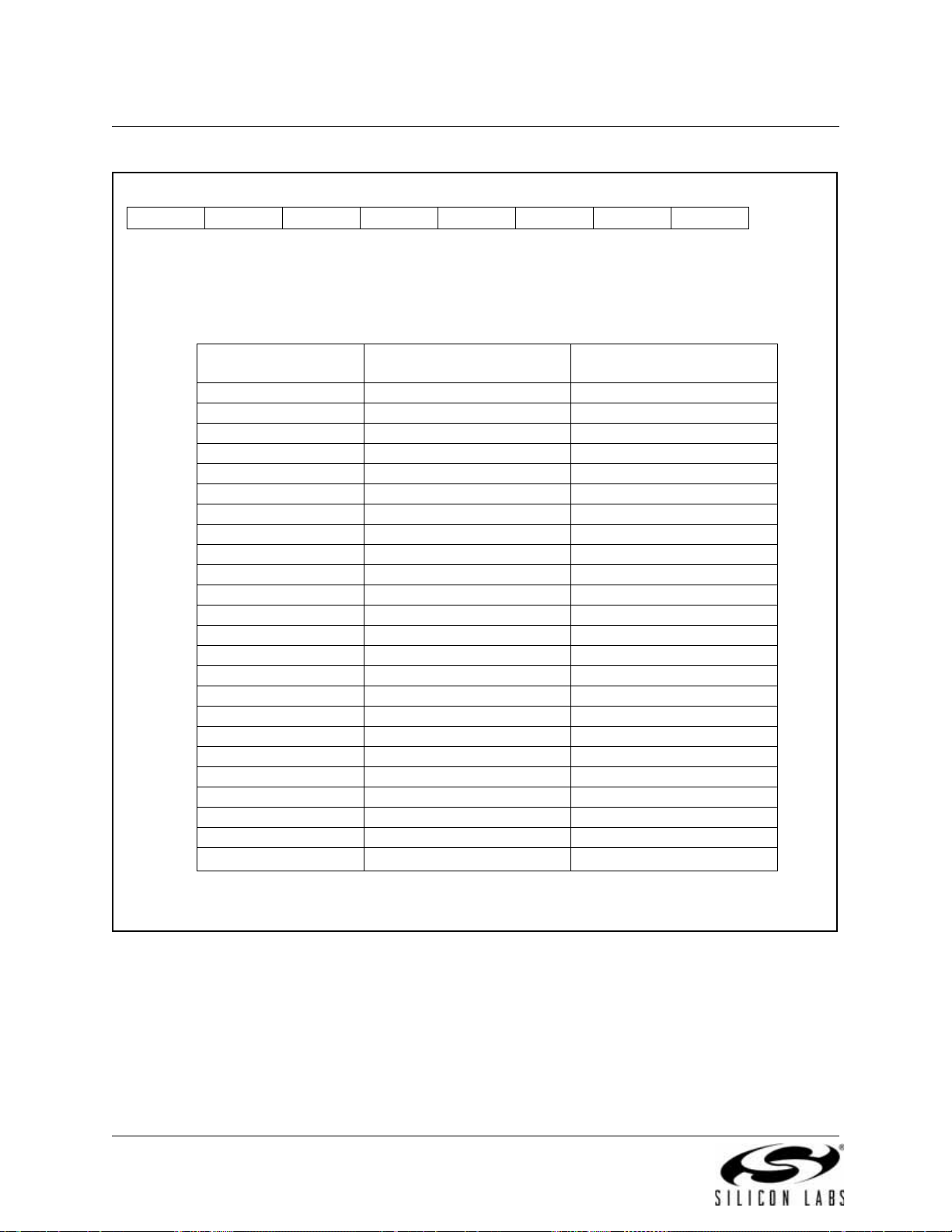
C8051F340/1/2/3/4/5/6/7/8/9/A/B/C/D
Bits7–5: UNUSED. Read = 000b; Write = don’t care.
Bits4–0: AMX0P4–0: AMUX0 Positive Input Selection
R R R R/W R/W R/W R/W R/W Reset Value
- - - AMX0P4 AMX0P3 AMX0P2 AMX0P1 AMX0P0 00000000
Bit7 Bit6 Bit5 Bit4 Bit3 Bit2 Bit1 Bit0 SFR Address:
0xBB
AMX0P4-0 ADC0 Positive Input
(32-pin Package)
ADC0 Positive Input
(48-pin Package)
00000 P1.0 P2.0
00001 P1.1 P2.1
00010 P1.2 P2.2
00011 P1.3 P2.3
00100 P1.4 P2.5
00101 P1.5 P2.6
00110 P1.6 P3.0
00111 P1.7 P3.1
01000 P2.0 P3.4
01001 P2.1 P3.5
01010 P2.2 P3.7
01011 P2.3 P4.0
01100 P2.4 P4.3
01101 P2.5 P4.4
01110 P2.6 P4.5
01111 P2.7 P4.6
10000 P3.0 RESERVED
10001 P0.0 P0.3
10010 P0.1 P0.4
10011 P0.4 P1.1
10100 P0.5 P1.2
10101 - 11101 RESERVED RESERVED
11110 Temp Sensor Temp Sensor
11111
V
DD
V
DD
SFR Definition 5.1. AMX0P: AMUX0 Positive Channel Select
48 Rev. 1.3
Page 49
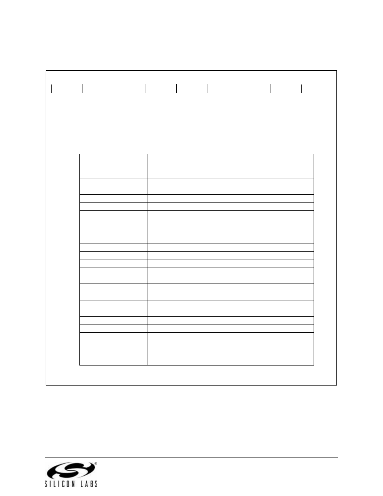
C8051F340/1/2/3/4/5/6/7/8/9/A/B/C/D
Bits7–5: UNUSED. Read = 000b; Write = don’t care.
Bits4–0: AMX0N4–0: AMUX0 Negative Input Selection.
Note that when GND is selected as the Negative Input, ADC0 operates in Single-ended
mode. For all other Negative Input selections, ADC0 operates in Differential mode.
R R R R/W R/W R/W R/W R/W Reset Value
- - - AMX0N4 AMX0N3 AMX0N2 AMX0N1 AMX0N0 00000000
Bit7 Bit6 Bit5 Bit4 Bit3 Bit2 Bit1 Bit0 SFR Address:
0xBA
AMX0N4-0 ADC0 Negative Input
(32-pin Package)
ADC0 Negative Input
(48-pin Package)
00000 P1.0 P2.0
00001 P1.1 P2.1
00010 P1.2 P2.2
00011 P1.3 P2.3
00100 P1.4 P2.5
00101 P1.5 P2.6
00110 P1.6 P3.0
00111 P1.7 P3.1
01000 P2.0 P3.4
01001 P2.1 P3.5
01010 P2.2 P3.7
01011 P2.3 P4.0
01100 P2.4 P4.3
01101 P2.5 P4.4
01110 P2.6 P4.5
01111 P2.7 P4.6
10000 P3.0 RESERVED
10001 P0.0 P0.3
10010 P0.1 P0.4
10011 P0.4 P1.1
10100 P0.5 P1.2
10101 - 11101 RESERVED RESERVED
11110 VREF VREF
11111 GND (Single-Ended Mode) GND (Single-Ended Mode)
SFR Definition 5.2. AMX0N: AMUX0 Negative Channel Select
Rev. 1.3 49
Page 50
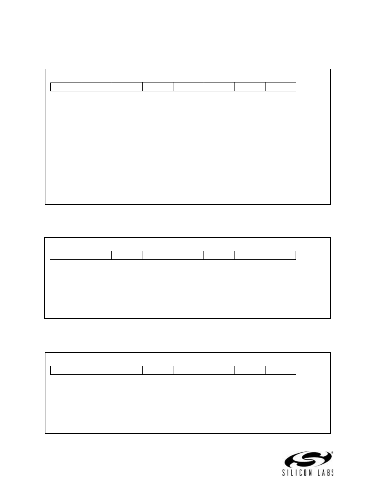
C8051F340/1/2/3/4/5/6/7/8/9/A/B/C/D
Bits7–3: AD0SC4–0: ADC0 SAR Conversion Clock Period Bits.
SAR Conversion clock is derived from system clock by the following equation, where
AD0SC refers to the 5-bit value held in bits AD0SC4-0. SAR Conversion clock requirement s
are given in Table 5.1.
Bit2: AD0LJST: ADC0 Left Justify Select.
0: Data in ADC0H:ADC0L registers are right-justified.
1: Data in ADC0H:ADC0L registers are left-justified.
Bits1–0: UNUSED. Read = 00b; Write = don’t care.
R/W R/W R/W R/W R/W R/W R/W R/W Reset Value
AD0SC4 AD0SC3 AD0SC2 AD0SC1 AD0SC0 AD0LJST - - 11111000
Bit7 Bit6 Bit5 Bit4 Bit3 Bit2 Bit1 Bit0 SFR Address:
0xBC
AD0SC
SYSCLK
CLK
SAR
----------------------
1–=
Bits7–0: ADC0 Data Word High-Order Bits.
For AD0LJST = 0: Bits 7–2 are the sign extension of Bit1. Bits 1-0 are the upper 2 bits of the
10-bit ADC0 Data Word.
For AD0LJST = 1: Bits 7–0 are the most-significant bits of the 10-bit ADC0 Data Word.
R/W R/W R/W R/W R/W R/W R/W R/W Reset Value
00000000
Bit7 Bit6 Bit5 Bit4 Bit3 Bit2 Bit1 Bit0 SFR Address:
0xBE
Bits7–0: ADC0 Data Word Low-Order Bits.
For AD0LJST = 0: Bits 7–0 are the lower 8 bits of the 10-bit Data Word.
For AD0LJST = 1: Bits 7–6 are the lower 2 bits of the 10-bit Data Word. Bits 5–0 will always
read ‘0’.
R/W R/W R/W R/W R/W R/W R/W R/W Reset Value
00000000
Bit7 Bit6 Bit5 Bit4 Bit3 Bit2 Bit1 Bit0 SFR Address:
0xBD
SFR Definition 5.3. ADC0CF: ADC0 Configuration
SFR Definition 5.4. ADC0H: ADC0 Data Word MSB
SFR Definition 5.5. ADC0L: ADC0 Data Word LSB
50 Rev. 1.3
Page 51

C8051F340/1/2/3/4/5/6/7/8/9/A/B/C/D
Bit7: AD0EN: ADC0 Enable Bit.
0: ADC0 Disabled. ADC0 is in low-power shutdown.
1: ADC0 Enabled. ADC0 is active and ready for data conversions.
Bit6: AD0TM: ADC0 Track Mode Bit.
0: Normal Track Mode: When ADC0 is enabled, tracking is continuous unless a conversion
is in progress.
1: Low-power Track Mode: Tracking Defined by AD0CM2-0 bits (see below).
Bit5: AD0INT: ADC0 Conversion Complete Interrupt Flag.
0: ADC0 has not completed a data conversion since the last time AD0INT was cleared.
1: ADC0 has completed a data conversion.
Bit4: AD0BUSY: ADC0 Busy Bit.
Read:
0: ADC0 conversion is complete or a conversion is not currently in progress. AD0INT is set
to logic 1 on the falling edge of AD0BUSY.
1: ADC0 conversion is in progress.
Write:
0: No Effect.
1: Initiates ADC0 Conversion if AD0CM2-0 = 000b
Bit3: AD0WINT: ADC0 Window Compare Interrupt Flag.
0: ADC0 Window Comparison Data match has not occurred since this flag was last cleared.
1: ADC0 Window Comparison Data match has occurred.
Bits2–0: AD0CM2–0: ADC0 Start of Conversion Mode Select.
When AD0TM = 0:
000: ADC0 conversion initiated on every write of ‘1’ to AD0BUSY.
001: ADC0 conversion initiated on overflow of Timer 0.
010: ADC0 conversion initiated on overflow of Timer 2.
011: ADC0 conversion initiated on overflow of Timer 1.
100: ADC0 conversion initiated on rising edge of external CNVSTR.
101: ADC0 conversion initiated on overflow of Timer 3.
11x: Reserved.
When AD0TM = 1:
000: Tracking initiated on write of ‘1’ to AD0BUSY and lasts 3 SAR clocks, followed by conversion.
001: Tracking initiated on overflow of Timer 0 and lasts 3 SAR clocks, followed by conversion.
010: Tracking initiated on overflow of Timer 2 and lasts 3 SAR clocks, followed by conversion.
011: Tracking initiated on overflow of Timer 1 and lasts 3 SAR clocks, followed by conversion.
100: ADC0 tracks only when CNVSTR input is logic low; conversion starts on rising CNVSTR edge.
101: Tracking initiated on overflow of Timer 3 and lasts 3 SAR clocks, followed by conversion.
11x: Reserved.
R/W R/W R/W R/W R/W R/W R/W R/W Reset Value
AD0EN AD0TM AD0INT AD0BUSY AD0WINT AD0CM2 AD0CM1 AD0CM0 00000000
Bit7 Bit6 Bit5 Bit4 Bit3 Bit2 Bit1 Bit0 SFR Address:
(bit addressable)
0xE8
SFR Definition 5.6. ADC0CN: ADC0 Control
Rev. 1.3 51
Page 52
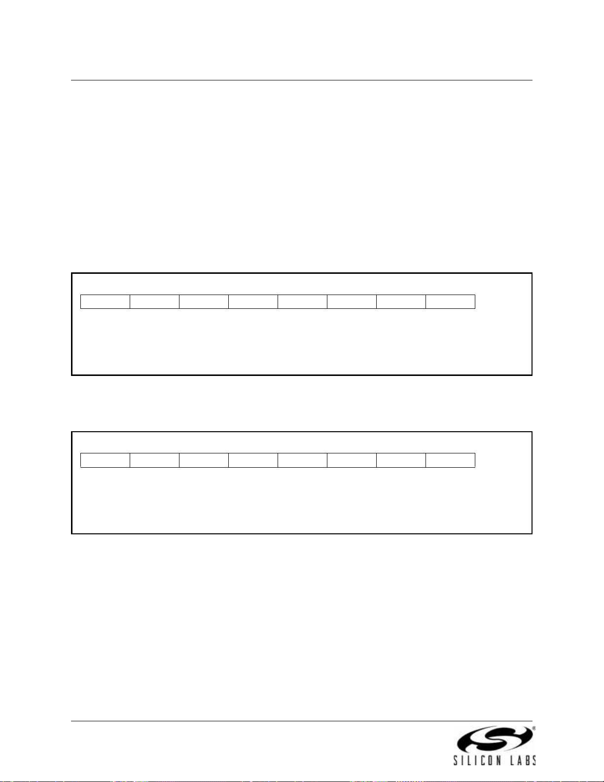
C8051F340/1/2/3/4/5/6/7/8/9/A/B/C/D
Bits7–0: High byte of ADC0 Greater-Than Data Word.
R/W R/W R/W R/W R/W R/W R/W R/W Reset Value
11111111
Bit7 Bit6 Bit5 Bit4 Bit3 Bit2 Bit1 Bit0 SFR Address:
0xC4
Bits7–0: Low byte of ADC0 Greater-Than Data Word.
R/W R/W R/W R/W R/W R/W R/W R/W Reset Value
11111111
Bit7 Bit6 Bit5 Bit4 Bit3 Bit2 Bit1 Bit0 SFR Address:
0xC3
5.4. Programmable Window Detector
The ADC Programmable Window Detector continuously compares the ADC0 conversion results to
user-programmed limits, and notifies the system when a desired condition is detected. This is especially
effective in an interrupt-driven system, saving code space and CPU bandwidth while delivering faster system response times. The window detector interrupt flag (A
in polled mode. The ADC0 Greater-Than (ADC0GTH, ADC0GTL) and Less-Than (ADC0LTH, ADC0LTL)
registers hold the comparison values. The window detector flag can be progra mmed to indicate when measured data is inside or outside of the user-program
Less-Than and ADC0 Greater-Than registers.
D0WINT in register ADC0CN) can also be used
med limits, depending on the contents of the ADC0
The Window Detector registers must be written with the same
as that of the current ADC configuration (left/right justified, single-ended/differential).
format (left/right justified, signed/unsigned)
SFR Definition 5.7. ADC0GTH: ADC0 Greater-Than Data High Byte
SFR Definition 5.8. ADC0GTL: ADC0 Greater-Than Data Low Byte
52 Rev. 1.3
Page 53
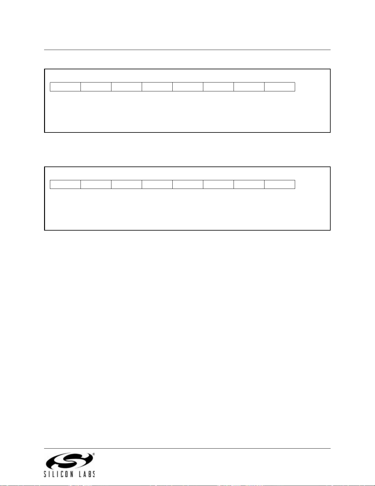
C8051F340/1/2/3/4/5/6/7/8/9/A/B/C/D
Bits7–0: High byte of ADC0 Less-Than Data Word.
R/W R/W R/W R/W R/W R/W R/W R/W Reset Value
00000000
Bit7 Bit6 Bit5 Bit4 Bit3 Bit2 Bit1 Bit0 SFR Address:
0xC6
Bits7–0: Low byte of ADC0 Less-Than Data Word.
R/W R/W R/W R/W R/W R/W R/W R/W Reset Value
00000000
Bit7 Bit6 Bit5 Bit4 Bit3 Bit2 Bit1 Bit0 SFR Address:
0xC5
SFR Definition 5.9. ADC0LTH: ADC0 Less-Than Data High Byte
SFR Definition 5.10. ADC0LTL: ADC0 Less-Than Data Low Byte
Rev. 1.3 53
Page 54
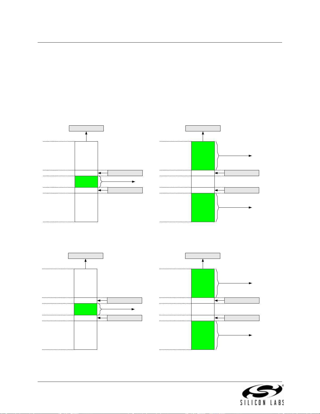
C8051F340/1/2/3/4/5/6/7/8/9/A/B/C/D
0x03FF
0x0081
0x0080
0x007F
0x0041
0x0040
0x003F
0x0000
0
Input Voltage
(Px.x - GND)
VREF x (1023/1024)
VREF x (128/1024)
VREF x (64/1024)
AD0WINT=1
AD0WINT
not affected
AD0WINT
not affected
ADC0LTH:ADC0LTL
ADC0GTH:ADC0GTL
0x03FF
0x0081
0x0080
0x007F
0x0041
0x0040
0x003F
0x0000
0
Input Voltage
(Px.x - GND)
VREF x (1023/1024)
VREF x (128/1024)
VREF x (64/1024)
AD0WINT
not affected
AD0WINT=1
AD0WINT=1
ADC0H:ADC0L ADC0H:ADC0L
ADC0GTH:ADC0GTL
ADC0LTH:ADC0LTL
0xFFC0
0x2040
0x2000
0x1FC0
0x1040
0x1000
0x0FC0
0x0000
0
Input Voltage
(Px.x - GND)
VREF x (1023/1024)
VREF x (128/1024)
VREF x (64/1024)
AD0WINT=1
AD0WINT
not affected
AD0WINT
not affected
ADC0LTH:ADC0LTL
ADC0GTH:ADC0GTL
0xFFC0
0x2040
0x2000
0x1FC0
0x1040
0x1000
0x0FC0
0x0000
0
Input Voltage
(Px.x - GND)
VREF x (1023/1024)
VREF x (128/1024)
VREF x (64/1024)
AD0WINT
not affected
AD0WINT=1
AD0WINT=1
ADC0H:ADC0L ADC0H:ADC0L
ADC0LTH:ADC0LTL
ADC0GTH:ADC0GTL
5.4.1. Window Detector In Single-Ended Mode
Figure 5.6 shows two example window comparisons for right-justified, single-ended data, with
ADC0LTH:ADC0LTL = 0x0080 (128d) and ADC0GTH:ADC0G TL = 0x0040 (64d). In single-ended mode,
input voltage can range from ‘0’ to VREF x (1023/1024) with respect to GND, and is represented by a
the
10-bit unsigned integer value. In the left example, an AD0WINT interrupt will be generated if the ADC0
conversion word (ADC0H:ADC0L) is within the range defined by ADC0GTH:ADC0GTL and
ADC0LTH:ADC0LTL (if 0x0040 < ADC0H:ADC0L < 0x0080). In the right example, and AD0WINT interrupt
will be generated
ADC0LT registers (if ADC0H:ADC0L < 0x0040 or ADC0H:ADC0L > 0x0080). Figure 5.7 shows an example using left-justified data with equivale
if the ADC0 conversion word is outside of the range defined by the ADC0GT and
nt ADC0GT and ADC0LT register settings.
Figure 5.6. ADC Window Compare Example: Right-Justified Single-Ended Data
Figure 5.7. ADC Window Compare Example: Left-Justified Single-Ended Data
54 Rev. 1.3
Page 55
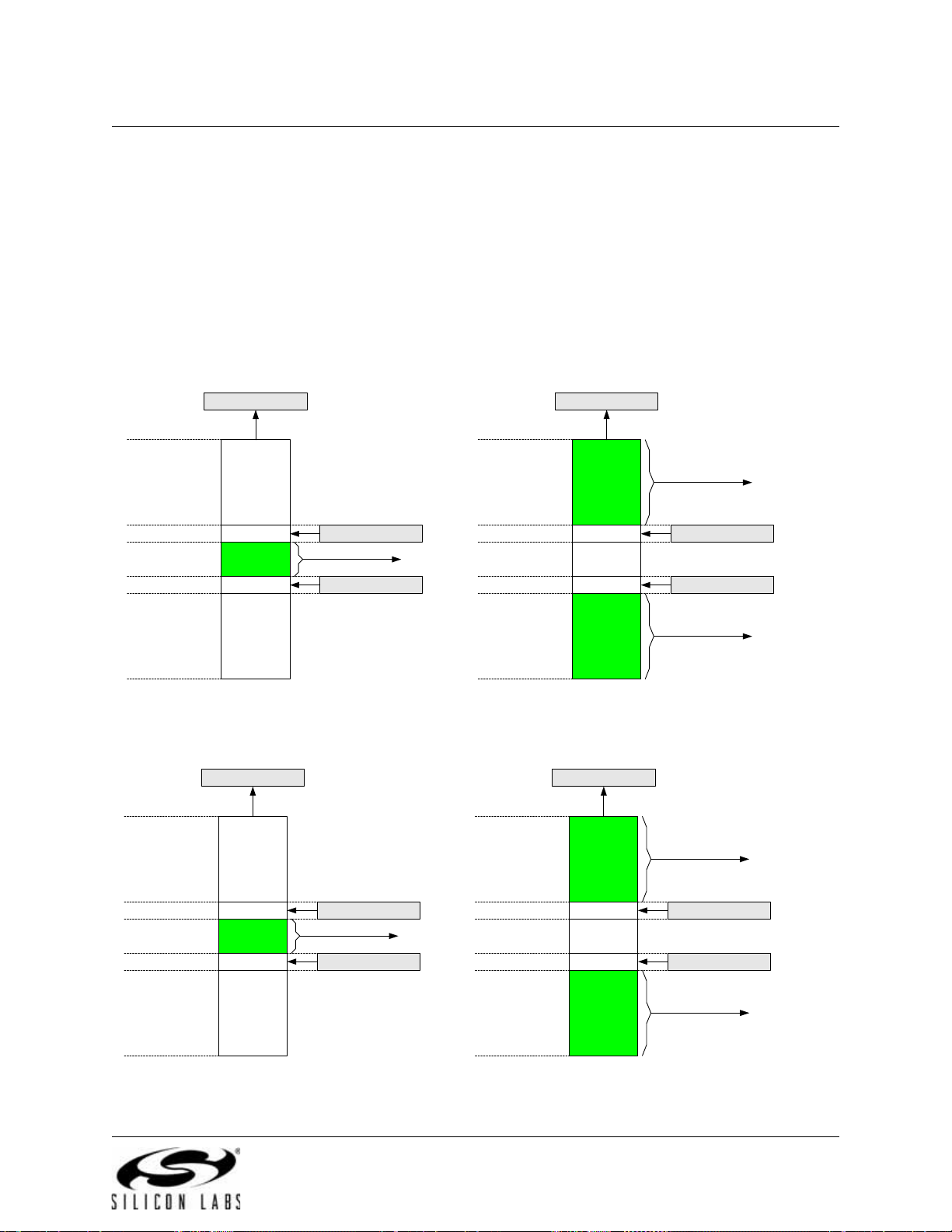
C8051F340/1/2/3/4/5/6/7/8/9/A/B/C/D
0x01FF
0x0041
0x0040
0x003F
0x0000
0xFFFF
0xFFFE
0x0200
-VREF
Input Voltage
(Px.x - Px.x)
VREF x (511/512)
VREF x (64/512)
VREF x (-1/512)
0x01FF
0x0041
0x0040
0x003F
0x0000
0xFFFF
0xFFFE
0x0200
-VREF
Input Voltage
(Px.x - Px.x)
VREF x (511/512)
VREF x (64/512)
VREF x (-1/512)
AD0WINT=1
AD0WINT
not affected
AD0WINT
not affected
ADC0LTH:ADC0LTL
ADC0GTH:ADC0GTL
AD0WINT
not affected
AD0WINT=1
AD0WINT=1
ADC0H:ADC0LADC0H:ADC0L
ADC0GTH:ADC0GTL
ADC0LTH:ADC0LTL
0x7FC0
0x1040
0x1000
0x0FC0
0x0000
0xFFC0
0xFF80
0x8000
-VREF
Input Voltage
(Px.x - Px.y)
VREF x (511/512)
VREF x (64/512)
VREF x (-1/512)
0x7FC0
0x1040
0x1000
0x0FC0
0x0000
0xFFC0
0xFF80
0x8000
-VREF
Input Voltage
(Px.x - Px.x)
VREF x (511/512)
VREF x (64/512)
VREF x (-1/512)
AD0WINT=1
AD0WINT
not affected
AD0WINT
not affected
ADC0LTH:ADC0LTL
ADC0GTH:ADC0GTL
AD0WINT
not affected
ADC0GTH:ADC0GTL
AD0WINT=1
AD0WINT=1
ADC0H:ADC0LADC0H:ADC0L
ADC0LTH:ADC0LTL
5.4.2. Window Detector In Differential Mode
Figure 5.8 shows two example window comparisons for right-justified, differential data, with
ADC0LTH:ADC0LTL = 0x0040 (+64d) and ADC0GTH:ADC0GTH = 0xFFFF (-1d). In differential mode, the
asurable voltage between the input pins is between -VREF a nd VREF*(511/512). Output codes are rep-
me
resented as 10-bit 2’s complement s
erated if the ADC0 conversion word
and ADC0LTH:ADC0LTL (if 0xFFFF (-1d) < ADC0H:ADC0L < 0x0040 (64d)). In the rig
AD0WINT interrupt will be generated if the ADC0 conversion word is outside of the range defined by the
ADC0GT and ADC0LT registers (if ADC0H:ADC0L < 0xFFFF (-1d) or ADC0H:ADC0L > 0x0040 (+64d)).
Figure 5.9 shows an example using left-justified data with equivalent ADC0GT and ADC0LT register settings.
igned integers. In the left example, an AD0WINT interrupt will be gen(ADC0H:ADC0L) is within the range defined by ADC0GTH:ADC0GTL
ht example, an
Figure 5.8. ADC Window Compare Example: Right-Justified Differential Data
Figure 5.9. ADC Window Compare Example: Left-Justified Differential Data
Rev. 1.3 55
Page 56
C8051F340/1/2/3/4/5/6/7/8/9/A/B/C/D
Table 5.1. ADC0 Electrical Characteristics
VDD = 3.0 V, VREF = 2.40 V, –40 to +85 °C unless otherwise specified
Parameter Conditions Min Typ Max Units
DC Accuracy
Resolution 10 bits
Integral Nonlinearity ±0.5 ±1 LSB
Differential Nonlinearity Guaranteed Monotonic ±0.5 ±1 LSB
Offset Error –15 0 +15 LSB
Full Scale Error –15 –1 +15 LSB
Offset Temperature Coefficient 10 ppm/°C
Dynamic Performance (10 kHz sine-wave Single-en
Signal-to-Noise Plus Distortion 51 52.5 dB
Total Harmonic Distortion
Up to the 5
th
harmonic
Spurious-Free Dynamic Range 78 dB
Conversion Rate
SAR Conversion Clock 3 MHz
Conversion Time in SAR Clocks 10 clocks
Track/Hold Acquisition Time 300 ns
Throughput Rate 200 ksps
Analog Inputs
ADC Input Voltage Range Single Ended (AIN+ – GND)
Differential (AIN+ – AIN–)
Absolute Pin V oltage with respect
to G
ND
Single Ended or Differential 0
Input Capacitance 5 pF
Temperature Sensor
Linearity
1
Gain 2.86 mV/°C
Gain Error
Offset
Offset Error
2
1
2
(Temp = 0 °C) 776 mV
Power Specifications
Power Supply Current (V
plied to ADC0)
DD
sup-
Operating Mode, 200 ksps 400 900 µA
Power Supply Rejection ±0.3 mV/V
ded input, 1 dB below Full Scale, 200 ksps)
–67 dB
0
–VREF
VREF
VREF
V
DD
V
V
V
±0.1 °C
±33.5 µV/ºC
±8.51 mV
Notes:
1. Includes ADC offset, gain, and linearity variations.
2. Re
presents one standard deviation from the mean.
56 Rev. 1.3
Page 57
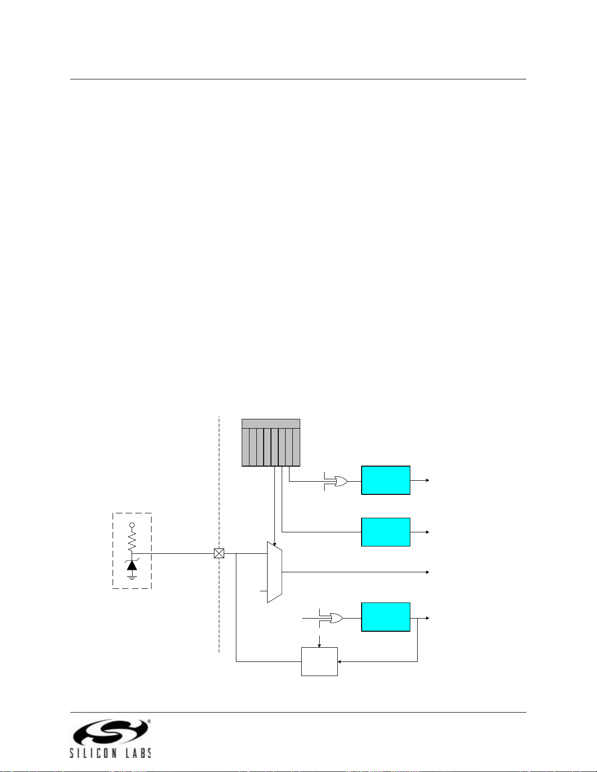
C8051F340/1/2/3/4/5/6/7/8/9/A/B/C/D
VREF
(to ADC)
To Analog Mux
VDD
VREF
R1
VDD
External
Voltage
Reference
Circuit
GND
Temp Sensor
EN
0
1
REF0CN
REFSL
TEMPE
BIASE
REFBE
REFBE
Internal
Reference
EN
Reference
Bias
EN
CLKMUL
Enable
TEMPE
To Clock Multiplier,
Temp Sensor
ADC Bias
To ADC,
Internal Oscillator
EN
IOSCEN
AD0EN
6. Voltage Reference (C8051F340/1/2/3/4/5/6/7/A/B Only)
The Voltage reference MUX on C8051F34x devices is configurable to use an externally conn ected vo ltage
reference, the on-chip reference voltage generator, or the power supply voltage V
REFSL bit in the Reference Control register (REF0CN) selects the reference source. For the internal refe rence or an external source, REFSL should be set to ‘0’; For V
as the reference source, REFSL should
DD
be set to ‘1’.
(see Figure 6.1). The
DD
The BIASE bit enables the internal ADC bias
generator, which is used by the ADC and Internal Oscillator.
This enable is forced to logic 1 when either of the aforementioned peripherals is enabled. The ADC bias
generator may be enabled manually by writing a ‘1’ to the BIASE bit in register REF0CN; see SFR Definition 6.1 for REF0CN register details. The Re
Voltage Reference, Temperature Sensor, and Clock Multiplier
ference bias generator (see Figure 6.1) is used by the Internal
. The Reference bias is automatically
enabled when any of the aforementioned peripherals are enabled. The electrical specifications for the voltage reference and bias circuits are given in Table 6.1.
Important Note About the VREF Pin: T
he VREF pin, when not using the on-chip voltage reference or an
external precision reference, ca n be co n fig ur ed a s a G P IO Po rt p in. Wh en u sin g an e xte r na l vo ltage ref erence or the on-chip reference, the VREF pin
should be configured as analog pin and skipped by the Digital
Crossbar. To configure the VREF pin for analog mode, set the corresponding bit in the PnMDIN register to
‘0’. To configure the Crossbar to skip the VREF pin, set the corresponding bit in register PnSKIP to ‘1’.
Refer to Section “15. Port Input/Output” on page 142 for complete Port I/O configuration details.
The temperature sensor connects to the ADC0 positive input multiplexe r (see Section “5.1. Analog Multi-
plexer” on page 42 for details). The TEMPE bit in register REF0CN enables/disables the temperature
sensor. While disabled, the temperature sensor defaults to a high impedance state and any ADC0 measurements performed on the sensor result in meanin gless data.
Figure 6.1. Voltage Reference Functional Block Diagram
Rev. 1.3 57
Page 58

C8051F340/1/2/3/4/5/6/7/8/9/A/B/C/D
Bits7–3: UNUSED. Read = 00000b; Write = don’t care.
Bit3: REFSL: Voltage Referenc e Sele ct .
This bit selects the source for the internal voltage reference.
0: VREF pin used as voltage reference.
1: V
DD
used as voltage reference.
Bit2: TEMPE: Temperature Sensor Enable Bit.
0: Internal Temperature Sensor off.
1: Internal Temperature Sensor on.
Bit1: BIASE: Internal Analog Bias Generator Enable Bit.
0: Internal Bias Generator off.
1: Internal Bias Generator on.
Bit0: REFBE: Internal Reference Buffer Enable Bit.
0: Internal Reference Buffer disabled.
1: Internal Reference Buffer enabled. Internal voltage reference driven on the VREF pin.
R/W R/W R/W R/W R/W R/W R/W R/W Reset Value
- - - - REFSL TEMPE BIASE REFBE 00000000
Bit7 Bit6 Bit5 Bit4 Bit3 Bit2 Bit1 Bit0 SFR Address:
0xD1
SFR Definition 6.1. REF0CN: Reference Control
Table 6.1. Voltage Reference Electrical Characteristics
VDD = 3.0 V; –40 to +85 °C Unless Otherwise Specified
Parameter Conditions Min Typ Max Units
Internal Reference (REFBE = 1)
Output Voltage 25 °C ambient 2.38 2.44 2.50 V
VREF Short-Circuit Current 10 mA
VREF Temperature Coeffi-
cient
Load Regulation Load = 0 to 200 µA to GND 1.5 ppm/µA
VREF Turn-on Time 1
VREF Turn-on Time 2 0.1 µF ceramic bypass 20 µs
VREF Turn-on Time 3 no bypass cap 10 µs
Power Supply Rejection 140 ppm/V
Input Voltage Range 0
Input Current
ADC Bias Generator BIASE = ‘1’ 100 µA
Reference Bias Generator 40 µA
58 Rev. 1.3
4.7 µF tantalum, 0.1 µF ceramic
ass
byp
External Reference (REFBE = 0)
Sample Rate = 200 ksps; VREF =
3.0 V
Bias Generators
15 ppm/°C
2 ms
V
DD
12 µA
V
Page 59

C8051F340/1/2/3/4/5/6/7/8/9/A/B/C/D
7. Comparators
C8051F34x devices include two on-chip programmable voltage Comparators. A block diagram of the comparators is shown in Figure 7.1, where “n” is the comparator number (0 or 1). The two Comparators operate identically with the following excep tions: (1) Their input sele ctions differ, and (2) Comparator0 can be
sed as a reset source. For input selection details, refer to SFR Definition 7.2 and SFR Definition 7.5.
u
Each Comparator offers pro grammable re sponse time a nd hysteresis, an an alog input multip lexer, and two
utputs that are optionally available at the Port pins: a synchronous “latched” output (CP0, CP1), or an
o
asynchronous “raw” output (CP0A, CP1A). The asynchronous signal is available even when the system
clock is not active. This allows the Comparators to operate and generate an output with the device in
STOP mode. When assigned to a Port pin, the Comparator outputs may be configured as open drain or
push-pull (see Section “15.2. Port I/O Initialization” on page 147). Comparator0 may also be used as a
reset source (see Section “11.5. Comparator0 Reset” on page 103).
The Comparator0 inputs are se lected in the CPT0 MX register (SFR Definition 7.2). The CMX0P1-CMX0P0
bits select the Comparator0 positive input; the CMX0N1input. The Comparator1 inputs are selected in the CPT1MX register (SFR Definition 7.5). The
CMX1P1-CMX1P0 bits select the Comparator1 positive input; the CMX1N1-CMX1N0 bits select the
mparator1 negative input.
Co
CMX0N0 bits select the Comparator0 negative
Important Note About Comparator Inputs: Th
figured as analog inputs in their associated Po rt configur
Crossbar (for details on Port configuration, see Section “15.3. General Purpose Port I/O” on page 150).
e Port pins selected as Comparator inputs should be con-
ation register , a nd config ured to be skipped by th e
Rev. 1.3 59
Page 60

C8051F340/1/2/3/4/5/6/7/8/9/A/B/C/D
VDD
CPTnCN
Reset Decision Tree
(Comprator 0 Only)
+
-
Crossbar
Interrupt
Logic
Q
Q
SET
CLR
D
Q
Q
SET
CLR
D
(SYNCHRONIZER)
GND
CPn +
CPn -
CPnEN
CPnOUT
CPnRIF
CPnFIF
CPnHYP1
CPnHYP0
CPnHYN1
CPnHYN0
CPTnMD
CPnRIE
CPnFIE
CPnMD1
CPnMD0
CPn
CPnA
CPn
Rising-edge
CPn
Falling-edge
CPn
Interrupt
CPnRIE
CPnFIE
CPTnMX
CMXnN1
CMXnN0
CMXnP1
CMXnP0
CMXnN2
CMXnP2
Port I/O connection options vary with
package (32-pin or 48-pin)
Comparator outputs can be polled in software, used as an interr upt source, and/or routed to a Port pin.
When routed to a Port pin, Comparator outputs are available asynchronous or synchronous to the system
clock; the asynchronous output is available even in STOP mode (with no system clock active). When disabled, the Comparator output (if assigned to a Port I/O pin via th
and supply current falls to less than 100 nA. See Section “15.1. Priority Crossbar Decoder” on
page 144 for details on configuring Comparator outputs via the dig
externally driven from –0.25 V to (V
trical specifications are given in Table 7.1.
Comparator response time may be configured in software via the CPTnMD registers (see SFR Definition
7.3 and SFR Definition 7.6). Selecting a longer response time reduce
Table 7.1 for complete timing and supply current specifications.
60 Rev. 1.3
Figure 7.1. Comparator Functional Block Diagram
) + 0.25 V without damage or upset. The complete Comparator elec-
DD
e Crossbar) defaults to the logic low state,
ital Crossbar . Comparator inputs can be
s the Comparator supply current. See
Page 61

C8051F340/1/2/3/4/5/6/7/8/9/A/B/C/D
Posi t ive Hystere sis Voltag e
(Programmed with CP0HYP Bits)
Negative Hysteresis Voltage
(Programmed by CP0HYN Bits)
VIN-
VIN+
INPUTS
CIRCUIT CONFIGURATION
+
_
CP0+
CP0-
CP0
VIN+
VIN-
OUT
V
OH
Posi t ive Hystere sis
Disabled
Maximum
Posi tive Hysteresis
Negative Hysteresis
Disabled
Maximum
Negative Hysteresis
OUTPUT
V
OL
Comparator hysteresis is programmed using Bits3-0 in the Comparator Control Register CPTnCN (shown
in SFR Definition 7.1 and SFR Definition 7.4). The amount of negative hyster
the settings of the CPnHYN bits. As shown in Figure 7.2, various levels of negative hysteresis can be
programmed, or negative hysteresis can be disabled. In a sim
determined by the setting the CPnHYP bits.
Comparator interrupts can be generated on
rupt enable and priority control, see Section “9.3. Interrupt Handler” on page 88.) The CPnFIF flag is set
to ‘1’ upon a Comparator falling-edge,
Once set, these bits remain set until cleared by software. The output state of the Comparator can be
obtained at any time by reading the CPnOUT bit. The Comparator is enabled by setting the CPnEN bit to
‘1’, and is disabled by clearing this bit to ‘0’.
Figure 7.2. Comparator Hysteresis Plot
ilar way, the amount of positive hysteresis is
both rising-edge and falling-edge output transitions. (For Inter-
and the CPnRIF flag is set to ‘1’ upon the Comparator rising-edge.
esis voltage is determined by
Rev. 1.3 61
Page 62

C8051F340/1/2/3/4/5/6/7/8/9/A/B/C/D
Bit7: CP0EN: Comparator0 Enable Bit.
0: Comparator0 Disabled.
1: Comparator0 Enabled.
Bit6: CP0OUT: Comparator0 Output State Flag.
0: Voltage on CP0+ < CP0–.
1: Voltage on CP0+ > CP0–.
Bit5: CP0RIF: Comparator0 Rising-Edge Flag.
0: No Comparator0 Rising Edge has occurred since this flag was last cleared.
1: Comparator0 Rising Edge has occurred.
Bit4: CP0FIF: Comparator0 Falling-Edge Flag.
0: No Comparator0 Falling-Edge has occurred since this flag was last cleared.
1: Comparator0 Falling-Edge Interrupt has occurred.
Bits3–2: CP0HYP1–0: Comparator0 Positive Hysteresis Control Bits.
00: Positive Hysteresis Disabled.
01: Positive Hysteresis = 5 mV.
10: Positive Hysteresis = 10 mV.
11: Positive Hysteresis = 20 mV.
Bits1–0: CP0HYN1–0: Comparator0 Negative Hysteresis Control Bits.
00: Negative Hysteresis Disabled.
01: Negative Hysteresis = 5 mV.
10: Negative Hysteresis = 10 mV.
11: Negative Hysteresis = 20 mV.
R/W R R/W R/W R/W R/W R/W R/W Reset Value
CP0EN CP0OUT CP0RIF CP0FIF CP0HYP1 CP0HYP0 CP0HYN1 CP0HYN0 00000000
Bit7 Bit6 Bit5 Bit4 Bit3 Bit2 Bit1 Bit0 SFR Address:
0x9B
SFR Definition 7.1. CPT0CN: Comparator0 Control
62 Rev. 1.3
Page 63

C8051F340/1/2/3/4/5/6/7/8/9/A/B/C/D
Bit7: UNUSED. Read = 0b, Write = don’t care.
Bits6–4: CMX0N2–CMX0N0: Comparator0 Negative Input MUX Select.
These bits select which Port pin is used as the Comparator0 negative input.
Bit3: UNUSED. Read = 0b, Write = don’t care.
Bits2–0: CMX0P2–CMX0P0: Comparator0 Positive Input MUX Select.
These bits select which Port pin is used as the Comparator0 positive input.
Note that the port pins used by the comparator depend on the package type (32-pin or 48-pin).
R/W R/W R/W R/W R/W R/W R/W R/W Reset Value
- CMX0N2 CMX0N1 CMX0N0 - CMX0P2 CMX0P1 CMX0P0 00000000
Bit7 Bit6 Bit5 Bit4 Bit3 Bit2 Bit1 Bit0 SFR Address:
0x9F
CMX0N1 CMX0N1 CMX0N0 Negative Input
(32-pin Package)
Negative Input
(48-pin Package)
0 0 0 P1.1 P2.1
0 0 1 P1.5 P2.6
0 1 0 P2.1 P3.5
0 1 1 P2.5 P4.4
1 0 0 P0.1 P0.4
CMX0P1 CMX0P1 CMX0P0 Positive Input
(32-pin Package)
Positive Input
(48-pin Package)
000 P1.0 P2.0
001 P1.4 P2.5
010 P2.0 P3.4
011 P2.4 P4.3
100 P0.0 P0.3
SFR Definition 7.2. CPT0MX: Comparator0 MUX Selection
Rev. 1.3 63
Page 64
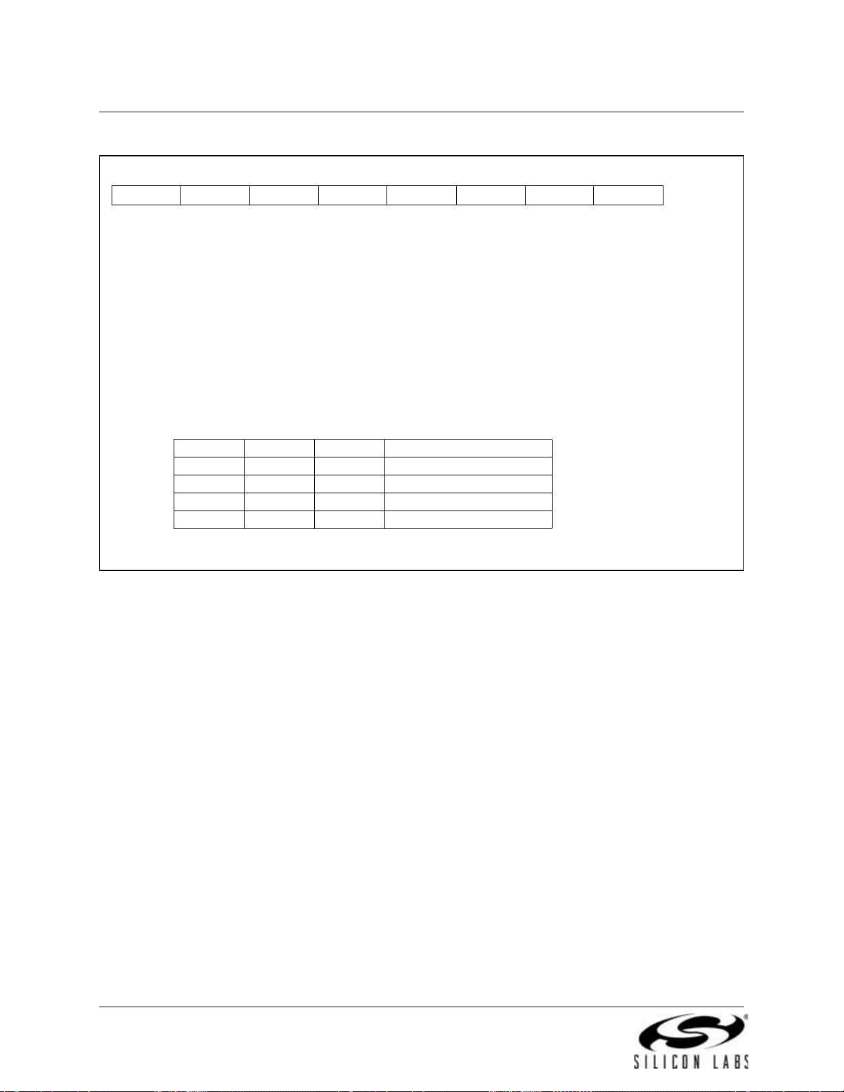
C8051F340/1/2/3/4/5/6/7/8/9/A/B/C/D
Bits7–6: UNUSED. Read = 00b. Write = don’t care.
Bit5: CP0RIE: Comparator0 Rising-Edge Interrupt Enable.
0: Comparator0 rising-edge interrupt disabled.
1: Comparator0 rising-edge interrupt enabled.
Bit4: CP0FIE: Comparator0 Falling-Edge Interrupt Enable.
0: Comparator0 falling-edge interrupt disabled.
1: Comparator0 falling-edge interrupt enabled.
Bits3–2: UNUSED. Read = 00b. Write = don’t care.
Bits1–0: CP0MD1–CP0MD0: Comparator0 Mode Select
These bits select the response time for Comparator0.
* See Table 7.1 for response time parameters.
R/W R/W R/W R/W R/W R/W R/W R/W Reset Value
- - CP0RIE CP0FIE - - CP0MD1 CP0MD0 00000010
Bit7 Bit6 Bit5 Bit4 Bit3 Bit2 Bit1 Bit0 SFR Address:
0x9D
Mode CP0MD1 CP0MD0 CP0 Response Time*
0 0 0 Fastest Response
101
210
311 Lowest Power
SFR Definition 7.3. CPT0MD: Comparator0 Mode Selection
64 Rev. 1.3
Page 65

C8051F340/1/2/3/4/5/6/7/8/9/A/B/C/D
Bit7: CP1EN: Comparator1 Enable Bit.
0: Comparator1 Disabled.
1: Comparator1 Enabled.
Bit6: CP1OUT: Comparator1 Output State Flag.
0: Voltage on CP1+ < CP1–.
1: Voltage on CP1+ > CP1–.
Bit5: CP1RIF: Comparator1 Rising-Edge Flag.
0: No Comparator1 Rising Edge has occurred since this flag was last cleared.
1: Comparator1 Rising Edge has occurred.
Bit4: CP1FIF: Comparator1 Falling-Edge Flag.
0: No Comparator1 Falling-Edge has occurred since this flag was last cleared.
1: Comparator1 Falling-Edge has occurred.
Bits3–2: CP1HYP1–0: Comparator1 Positive Hysteresis Control Bits.
00: Positive Hysteresis Disabled.
01: Positive Hysteresis = 5 mV.
10: Positive Hysteresis = 10 mV.
11: Positive Hysteresis = 20 mV.
Bits1–0: CP1HYN1–0: Comparator1 Negative Hysteresis Control Bits.
00: Negative Hysteresis Disabled.
01: Negative Hysteresis = 5 mV.
10: Negative Hysteresis = 10 mV.
11: Negative Hysteresis = 20 mV.
R/W R R/W R/W R/W R/W R/W R/W Reset Value
CP1EN CP1OUT CP1RIF CP1FIF CP1HYP1 CP1HYP0 CP1HYN1 CP1HYN0 00000000
Bit7 Bit6 Bit5 Bit4 Bit3 Bit2 Bit1 Bit0 SFR Address:
0x9A
SFR Definition 7.4. CPT1CN: Comparator1 Control
Rev. 1.3 65
Page 66
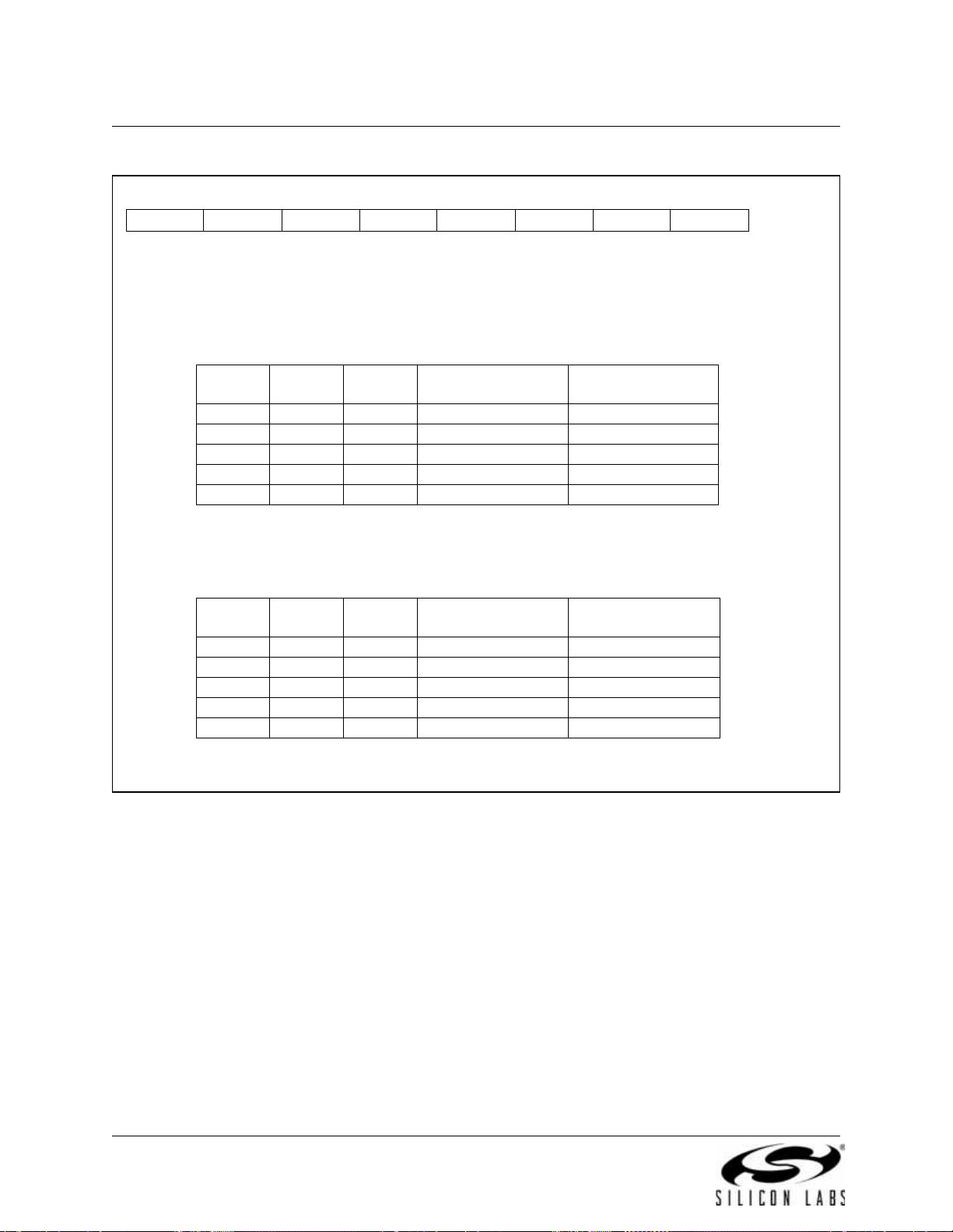
C8051F340/1/2/3/4/5/6/7/8/9/A/B/C/D
Bit7: UNUSED. Read = 0b, Write = don’t care.
Bits6–4: CMX1N2–CMX1N0: Comparator1 Negative Input MUX Select.
These bits select which Port pin is used as the Comparator1 negative input.
Bit3: UNUSED. Read = 0b, Write = don’t care.
Bits2–0: CMX1P1–CMX1P0: Comparator1 Positive Input MUX Select.
These bits select which Port pin is used as the Comparator1 positive input.
Note that the port pins used by the comparator depend on the pa ckage type (32-pin or 48-pin).
R/W R/W R/W R/W R/W R/W R/W R/W Reset Value
- CMX1N2 CMX1N1 CMX1N0 - CMX1P2 CMX1P1 CMX1P0 00000000
Bit7 Bit6 Bit5 Bit4 Bit3 Bit2 Bit1 Bit0 SFR Address:
0x9E
CMX1N2 CMX1N1 CMX1N0 Negative Input
(32-pin Package)
Negative Input
(48-pin Package)
000 P1.3 P2.3
001 P1.7 P3.1
010 P2.3 P4.0
011 P2.7 P4.6
100 P0.5 P1.2
CMX1P2 CMX1P1 CMX1P0 Positive Input
(32-pin Package)
Positive Input
(48-pin Package)
0 0 0 P1.2 P2.2
0 0 1 P1.6 P3.0
0 1 0 P2.2 P3.7
0 1 1 P2.6 P4.5
1 0 0 P0.4 P1.1
SFR Definition 7.5. CPT1MX: Comparator1 MUX Selection
66 Rev. 1.3
Page 67
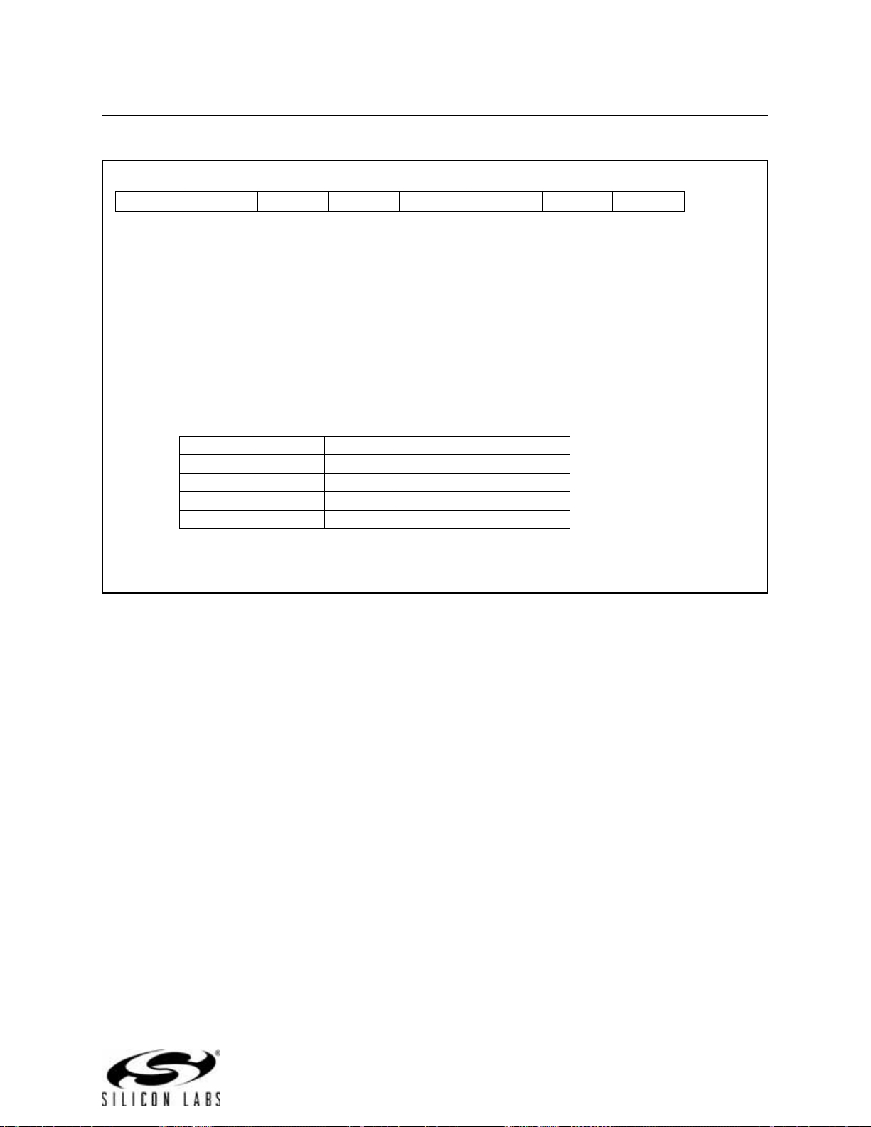
C8051F340/1/2/3/4/5/6/7/8/9/A/B/C/D
Bits7–6: UNUSED. Read = 00b, Write = don’t care.
Bit5: CP1RIE: Comparator1 Rising-Edge Interrupt Enable.
0: Comparator1 rising-edge interrupt disabled.
1: Comparator1 rising-edge interrupt enabled.
Bit4: CP1FIE: Comparator1 Falling-Edge Interrupt Enable.
0: Comparator1 falling-edge interrupt disabled.
1: Comparator1 falling-edge interrupt enabled.
Bits1–0: CP1MD1–CP1MD0: Comparator1 Mode Select.
These bits select the response time for Comparator1.
* See Table 7.1 for response time parameters.
R/W R/W R/W R/W R/W R/W R/W R/W Reset Value
- - CP1RIE CP1FIE - - CP1MD1 CP1MD0 00000010
Bit7 Bit6 Bit5 Bit4 Bit3 Bit2 Bit1 Bit0 SFR Address:
0x9C
Mode CP1MD1 CP1MD0 CP1 Response Time*
0 0 0 Fastest Response
101
210
311 Lowest Power
SFR Definition 7.6. CPT1MD: Comparator1 Mode Selection
Rev. 1.3 67
Page 68
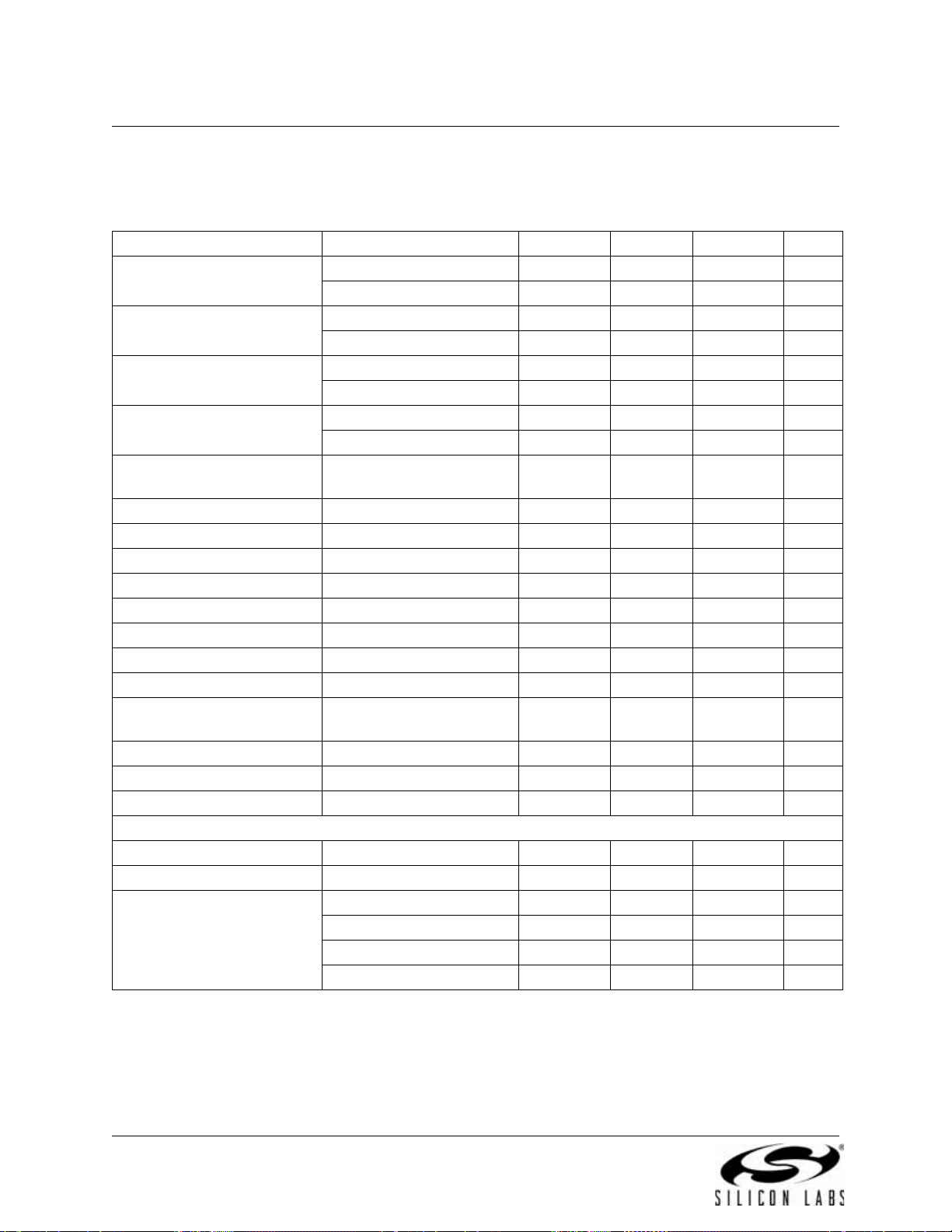
C8051F340/1/2/3/4/5/6/7/8/9/A/B/C/D
Table 7.1. Comparator Electrical Characteristics
VDD = 3.0 V, –40 to +85 °C unless otherwise noted.
All specifications apply to both Comparator0 and Comparator1 unless otherwise noted.
Parameter Conditions Min Typ Max Units
Response Time:
Mode 0, Vcm* = 1.5 V
Response Time:
Mode 1, Vcm* = 1.5 V
Response Time:
Mode 2, Vcm* = 1.5 V
Response Time:
Mode 3, Vcm* = 1.5 V
Common-Mode Rejection
Ratio
Positive Hysteresis 1 CP0HYP1–0 = 00 0 1 mV
Positive Hysteresis 2 CP0HYP1–0 = 01 2 5 10 mV
Positive Hysteresis 3 CP0HYP1–0 = 10 7 10 20 mV
Positive Hysteresis 4 CP0HYP1–0 = 11 15 20 30 mV
Negative Hysteresis 1 CP0HYN1–0 = 00 0 1 mV
Negative Hysteresis 2 CP0HYN1–0 = 01 2 5 10 mV
Negative Hysteresis 3 CP0HYN1–0 = 10 7 10 20 mV
Negative Hysteresis 4 CP0HYN1–0 = 11 15 20 30 mV
Inverting or Non-Inverting
Inpu
t Voltage Range
Input Capacitance 3 pF
Input Bias Current 0.001 nA
Input Offset Voltage –5 +5 mV
Power Supply Rejection 0.1 mV/V
Power-up Time 10 µs
Supply Current at DC
CP0+ – CP0– = 100 mV 100 ns
CP0+ – CP0– = –100 mV 250 ns
CP0+ – CP0– = 100 mV 175 ns
CP0+ – CP0– = –100 mV 500 ns
CP0+ – CP0– = 100 mV 320 ns
CP0+ – CP0– = –100 mV 1100 ns
CP0+ – CP0– = 100 mV 1050 ns
CP0+ – CP0– = –100 mV 5200 ns
1.5 4 mV/V
+ 0.25
–0.25
Power Supply
Mode 0 7.6 µA
Mode 1 3.2 µA
Mode 2 1.3 µA
Mode 3 0.4 µA
V
DD
V
*Note: Vcm is the common-mode voltage on CP0+ and CP0–.
68 Rev. 1.3
Page 69
C8051F340/1/2/3/4/5/6/7/8/9/A/B/C/D
8. Voltage Regulator (REG0)
C8051F34x devices include a voltage regulator (REG0). When enabled, the REG0 output appears on the
pin and can be used to power external devi ces. REG0 can be en abled/disa bled by software using bit
V
DD
REGEN in register REG0CN. See Table 8.1 for REG0 electrical characteristics.
Note that the VBUS signal must be connected to the VBUS pin
when using the device in a USB network.
The VBUS signal should only be connected to the REGIN pin when operating the device as a bus-powere d
function. REG0 configuration options are shown in Figure 8.1–Figure 8.4.
8.1. Regulator Mode Selection
REG0 offers a low power mode intended for use when the device is in suspend mode. In this low power
mode, the REG0 output remains as specified; however the REG0 dynami c performa nce (respo nse time) is
degraded. See Table 8.1 for normal and low power mode supply cu
selection is controlled via the REGMOD
bit in register REG0CN.
rrent specifications. The REG0 mode
8.2. VBUS Detection
When the USB Function Controller is used (see section Section “16. Universal Serial Bus Controller
(USB0)” on page 159), the VBUS signal should be connected to the VBUS pin.
REG0CN) indicates the current logic level of the VBUS s
ignal. If enabled, a VBUS interrupt will be generated when the VBUS signal matches the polarity selected by the VBPOL bit in register REG0CN. The
VBUS
interrupt is level-sensitive, and has no associated interrupt pending flag. The VBUS interrupt will be
active as long as the VBUS signal matc hes the polarity selected by VBPOL. See Table 8.1 for VBUS input
parameters.
Important Note: When USB is
selected as a reset source, a system reset will be generated when the
VBUS signal matches the polarity selected by the VBPOL bit. See Section “11. Reset Sources” on
page 100 for details on selecting USB as a reset source
The VBSTAT bit (register
Table 8.1. Voltage Regulator Electrical Specifications
–40 to +85 °C unless otherwise specified.
Parameter Conditions Min Typ Max Units
Input Voltage Range
Output Voltage (V
Output Current
1
2
)
DD
2
Output Current = 1 to 100 mA 3.0 3.3 3.6 V
VBUS Detection Input Low Voltage 1.0 V
VBUS Detection Input High Voltage 3.0 V
Bias Current
3
Dropout Voltage (V
Notes:
1. Inpu
2. Output cu
3. The minimum input voltage is 2.70 V or VDD + VDO (max load), whichever is greater.
t range specified for regulation. When an external regulator is used, should be tied to VDD.
)
DO
rrent is total regulator output, including any current required by the C8051F34x.
Normal Mode (REGMOD = ‘0’)
Low Power Mode (REGMOD = ‘1’)
Rev. 1.3 69
2.7 5.25 V
100 mA
65
35
111
61
µA
1 mV/mA
Page 70
C8051F340/1/2/3/4/5/6/7/8/9/A/B/C/D
Voltage Regulator (REG0)5 V In
3 V Out
VBUS Sense
REGIN
VBUS
From VBUS
To 3 V
Power Net
Device
Power Net
VDD
Voltage Regulator (REG0)5 V In
3 V Out
VBUS Sense
REGIN
VBUS
To 3 V
Power Net
Device
Power Net
VDD
From 5 V
Power Net
From VBUS
Figure 8.1. REG0 Configuration: USB Bus-Powered
Figure 8.2. REG0 Configuration: USB Self-Powered
70 Rev. 1.3
Page 71
C8051F340/1/2/3/4/5/6/7/8/9/A/B/C/D
Voltage Regulator (REG0)5 V In
3 V Out
VBUS Sense
REGIN
VBUS
From 3 V
Power Net
Device
Power Net
VDD
From VBUS
Voltage Regulator (REG0)5 V In
3 V Out
VBUS Sense
REGIN
VBUS
To 3 V
Power Net
Device
Power Net
VDD
From 5 V
Power Net
Figure 8.3. REG0 Configuration: USB Self-Powered, Regulator Disabled
Figure 8.4. REG0 Configuration: No USB Connection
Rev. 1.3 71
Page 72

C8051F340/1/2/3/4/5/6/7/8/9/A/B/C/D
Bit7: REGDIS: Voltage Regulator Disable.
0: Voltage Regulator Enabled.
1: Voltage Regulator Disabled.
Bit6: VBSTAT: VBUS Signal Status.
0: VBUS signal currently absent (device not attached to USB network).
1: VBUS signal currently present (device attached to USB network).
Bit5: VBPOL: VBUS Interrupt Polarity Select.
This bit selects the VBUS interrupt polarity.
0: VBUS interrupt active when VBUS is low.
1: VBUS interrupt active when VBUS is high.
Bit4: REGMOD: Voltage Regulator Mode Select.
This bit selects the Voltage Regulator mode. When REGMOD is set to ‘1’, the voltage regulator operates in low power (suspend) mode.
0: USB0 Voltage Regulator in normal mode.
1: USB0 Voltage Regulator in low power mode.
Bits3–0: Reserved. Read = 0000b. Must Write = 0000b.
R/W R R/W R/W R/W R/W R/W R/W Reset Value
REGDIS VBSTAT VBPOL REGMOD Reserved Reserved Reserved Reserved 00000000
Bit7 Bit6 Bit5 Bit4 Bit3 Bit2 Bit1 Bit0 SFR Address:
0xC9
SFR Definition 8.1. REG0CN: Voltage Regulator Control
72 Rev. 1.3
Page 73
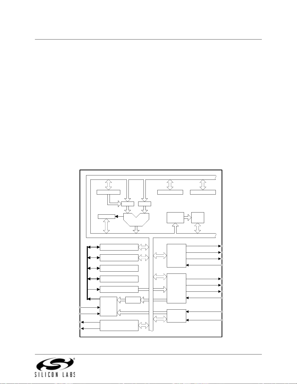
C8051F340/1/2/3/4/5/6/7/8/9/A/B/C/D
- Fully Compatible with MCS-51 Instruction
Set
- 0 to 48 MHz Clock Frequency
- 256 Bytes of Internal RAM
- 25 Port I/O
- Extended Interrupt Handler
- Reset Input
- Power Management Modes
- On-chip Debug Logic
- Program and Data Memory Security
DATA BUS
TMP1 TMP2
PRGM. ADDRESS REG.
PC INCREMENTER
ALU
PSW
DATA BUS
DATA BUS
MEMORY
INTERFACE
MEM_ADDRESS
D8
PIPELINE
BUFFER
DATA POINTER
INTERRUPT
INTERFACE
SYSTEM_IRQs
EMULATION_IRQ
MEM_CONTROL
CONTROL
LOGIC
A16
PROGRAM COUNTER (PC)
STOP
CLOCK
RESET
IDLE
POWER CONTROL
REGISTER
DATA BUS
SFR
BUS
INTERFACE
SFR_ADDRESS
SFR_CONTROL
SFR_WRITE_DATA
SFR_READ_DATA
D8
D8
B REGISTER
D8
D8
ACCUMULATOR
D8
D8
D8
D8
D8
D8
D8
D8
MEM_WRITE_DATA
MEM_READ_DATA
D8
SRAM
ADDRESS
REGISTER
SRAM
(256 X 8)
D8
STACK POINTER
D8
9. CIP-51 Microcontroller
The MCU system controller core is the CIP-51 microcontroller. The CIP-51 is fully compatible with the
MCS-51™ instruction set; standard 803x/805x assemblers and compilers can be used to develop software. The MCU family has a superset of all the peripherals included with a standard 8051. Included are
r 16-bit counter/timers (see description in Section 21), an enhanced full-duplex UART (see description
fou
in Section 18), an Enhanced SPI (see description in Section 20), 256 bytes of internal RAM, 128 byte
Special Function Register (SFR) address space (Section 9.2.6), and 25 Port I/O (see description in Sec-
tion 15). The CIP-51 also includes on-chip debug hardware (see description in Se ction 23 ), and interf aces
directly with the analog and digit
solution in a single integrated circuit.
The CIP-51 Microcontroller core implements the standard 8051 organization and peripherals as well as
additional c
ustom peripherals and functions to extend its capability (see Figure 9.1 for a block diagram).
The CIP-51 includes the following features:
al subsystems providing a complete data acquisition or control-system
Figure 9.1. CIP-51 Block Diagram
Rev. 1.3 73
Page 74

C8051F340/1/2/3/4/5/6/7/8/9/A/B/C/D
Performance
The CIP-51 employs a pipelined architecture that gre a tly increases its instruction throughput over the stan dard 8051 architecture. In a standard 8051, all inst
clock cycles to execute, and usually have a maximum system clock of 12 MHz. By contrast, the CIP-51
core exec
than eight system clock cycles.
With the CIP-51's maximum system clock at 25 MHz, it has a peak throughput of 25 MIPS. The CIP-51 has
total of 109 instructions. The table below shows the total number of instructions that for execution time.
a
Programming and Debugging Support
In-system programming of the Flash program memory and communication with on-chip debug support
logic is ac
mable Flash can also be read and changed a single byte
MOVC and MOVX instructions. T his feat ure allows progra m me mory to be us ed for no n-volatile data storage as well as updating program code under software control.
utes 70% of its instructions in one or two system clock cycles, with no instructions taking more
Clocks to Execute 1 2 2/4 3 3/5 4 5 4/6 6 8
Number of Instructions 26 50 5 10 7 5 2 1 2 1
complished via the Silicon Labs 2-Wire Development Interface (C2). Note that the re-program-
ructions except for MUL and DIV take 12 or 24 system
at a time by the application software using the
The on-chip Silicon Labs 2-Wire (C2) D
resources), full speed, in-circuit debugging using the production MCU installed in the final application. This
debug logic supports inspection and modification of memory and registers, setting breakpoints, single
stepping, run and halt commands. All ana log and digital peripherals are fully functional while debugging
using C2. The two C2 interface pins can be shared with user functions, allowing in-system debugging without occupying package pins. C2 details can be found in Section “23. C2 Interface” on page 271.
The CIP-51 is supported by devel
vides an integrated development environment (IDE) including editor, debugger, and programmer. The
debugger and programmer interface to the CIP-51 via the C2 interface to provide fast and efficient
IDE's
in-system device programming and debugging. An 8051 assembler, linker and evaluation ‘C’ compiler are
included in the Development Kit. Many third party macro assemblers and C compilers are also available,
which can be used directly with the IDE.
opment tools from Silicon Labs and third party vendors. Silicon Labs pro-
evelopment Interface allows non-intrusive (uses no on-chip
9.1. Instruction Set
The instruction set of the CIP-51 System Controller is fully compatible with the standard MCS-51™ instruction set. Standard 8051 development tools can be used to develop software for the CIP-51. All CIP-51
structions are the binary and functional equivalent of their MCS-51™ counterparts, including opcodes,
in
addressing modes and effect on PSW flags. However, instruction timing is different than that of the standard 8051.
9.1.1. Instruction and CPU Timing
In many 8051 implementations, a distinction is made between machine cycles and clock cycles, with
machine cycles varying from 2 to 12 clock cycles in length. However, the CIP-51 implementation is based
solely on clock cycle timing. All instruction timings are specified in terms of clock cycles.
Due to the pipelined architecture of the CIP-51, most in
cycles as there are program bytes in the instruction. Conditional branch instructions take two fewer clock
cycles to complete when the branch is not taken as opposed to when the branch is taken. Table 9.1 is the
CIP-51 Instruction Set Summary, which includes the mn
cycles for each instruction.
74 Rev. 1.3
structions execute in the same number of clo ck
emonic, number of bytes, and number of clock
Page 75

C8051F340/1/2/3/4/5/6/7/8/9/A/B/C/D
9.1.2. MOVX Instruction and Program Memory
In the CIP-51, the MOVX instruction serves th ree purposes: accessing on-chip XRAM, accessing off-chip
data XRAM (only on C8051F340/1/4/5/8 devices), and accessing on-chip program Flash memory. The
Flash access feature provides a mechanism for user software to update program code and use the program memory space for non-volatile data storage (see Section “12. Flash Memory” on page 107). The
External Memory Interface (only on C8051F340/1/4/5/8 devices) provides a fast access interface to
f-chip data XRAM (or memory-mapped peripherals) via the MOVX instruction. Refer to Section
of
“13. External Data Memory Inter face and On-Chip XRAM” on
Table 9.1. CIP-51 Instruction Set Summary
page 114. for details.
Mnemonic Description Bytes
Arithmetic Operations
ADD A, Rn Add register to A 1 1
ADD A, direct Add direct byte to A 2 2
ADD A, @Ri Add indirect RAM to A 1 2
ADD A, #data Add immediate to A 2 2
ADDC A, Rn Add register to A with carry 1 1
ADDC A, direct Add direct byte to A with carry 2 2
ADDC A, @Ri Add indirect RAM to A with carry 1 2
ADDC A, #data Add immediate to A with carry 2 2
SUBB A, Rn Subtract register fro m A with bo rr ow 1 1
SUBB A, direct Subtract direct byte from A with borrow 2 2
SUBB A, @Ri Subtract indirect RAM from A with borrow 1 2
SUBB A, #data Subtract imm e dia te fro m A with bo rr ow 2 2
INC A Increment A 1 1
INC Rn Increment register 1 1
INC direct Increment direct byte 2 2
INC @Ri Increment indirect RAM 1 2
DEC A Decrement A 1 1
DEC Rn Decrement register 1 1
DEC direct Decrement direct byte 2 2
DEC @Ri Decrement indirect RAM 1 2
INC DPTR Increment Data Pointer 1 1
MUL AB Multiply A and B 1 4
DIV AB Divide A by B 1 8
DA A Decimal adjust A 1 1
Logical Operations
ANL A, Rn AND Register to A 1 1
ANL A, direct AND direct byte to A 2 2
ANL A, @Ri AND indirect RAM to A 1 2
ANL A, #data AND immediate to A 2 2
ANL direct, A AND A to direct byte 2 2
ANL direct, #data AND immediate to direct byte 3 3
ORL A, Rn OR Register to A 1 1
ORL A, direct OR direct byte to A 2 2
ORL A, @Ri OR indirect RAM to A 1
Clock
Cycles
2
Rev. 1.3 75
Page 76

C8051F340/1/2/3/4/5/6/7/8/9/A/B/C/D
Table 9.1. CIP-51 Instruction Set Summary (Continued)
Mnemonic Description Bytes
ORL A, #data OR immediate to A 2 2
ORL direct, A OR A to direct byte 2 2
ORL direct, #data OR immediate to direct byte 3 3
XRL A, Rn Exclusive-OR Register to A 1 1
XRL A, direct Exclusive-OR direct byte to A 2 2
XRL A, @Ri Exclusive-OR indirect RAM to A 1 2
XRL A, #data Exclusive-OR immediate to A 2 2
XRL direct, A Exclusive-OR A to direct byte 2 2
XRL direct, #data Exclusive-OR immediate to direct byte 3 3
CLR A Clear A 1 1
CPL A Complement A 1 1
RL A Rotate A left 1 1
RLC A Rotate A left through Carry 1 1
RR A Rotate A right 1 1
RRC A Rotate A right through Carry 1 1
SWAP A Swap nibbles of A 1 1
Data Transfer
MOV A, Rn Move Register to A 1 1
MOV A, direct Move direct byte to A 2 2
MOV A, @Ri Move indirect RAM to A 1 2
MOV A, #data Move immediate to A 2 2
MOV Rn, A Move A to Register 1 1
MOV Rn, direct Move direct byte to Register 2 2
MOV Rn, #data Move immediate to Register 2 2
MOV direct, A Move A to direct byte 2 2
MOV direct, Rn Move Register to direct byte 2 2
MOV direct, direct Move direct byte to direct byte 3 3
MOV direct, @Ri Move indirect RAM to direct byte 2 2
MOV direct, #data Move immediate to direct byte 3 3
MOV @Ri, A Move A to indirect RAM 1 2
MOV @Ri, direct Move direct byte to indirect RAM 2 2
MOV @Ri, #data Move immediate to indirect RAM 2 2
MOV DPTR, #data16 Load DPTR with 16-bit constant 3 3
MOVC A, @A+DPTR Move code byte relative DPTR to A 1 3
MOVC A, @A+PC Move code byte relative PC to A
MOVX A, @Ri Move external data (8-bit address) to A 1 3
MOVX @Ri, A Move A to external data (8-bit address) 1 3
MOVX A, @DPTR Move external data (16-bit address) to A 1 3
MOVX @DPTR, A Move A to external data (16-bit address) 1 3
PUSH direct Push direct byte onto stack 2 2
POP direct Pop direct byte from stack 2 2
XCH A, Rn Exchange Register with A 1 1
XCH A, direct Exchange direct byte with A 2 2
XCH A, @Ri Exchange indirect RAM with A 1 2
XCHD A, @Ri Exchange low nibble of indirect RAM with A 1 2
1 3
Clock
Cycles
76 Rev. 1.3
Page 77

C8051F340/1/2/3/4/5/6/7/8/9/A/B/C/D
Table 9.1. CIP-51 Instruction Set Summary (Continued)
Mnemonic Description Bytes
Boolean Manipulation
CLR C Clear Carry 1 1
CLR bit Clear direct bit 2 2
SETB C Set Carry 1 1
SETB bit Set direct bit 2 2
CPL C Complement Carry 1 1
CPL bit Complement direct bit 2 2
ANL C, bit AND direct bit to Carry 2 2
ANL C, /bit AND complement of direct bit to Carry 2 2
ORL C, bit OR direct bit to carry 2 2
ORL C, /bit OR complement of direct bit to Carry 2 2
MOV C, bit Move direct bit to Carry 2 2
MOV bit, C Move Carry to direct bit 2 2
JC rel Jump if Carry is set 2 2/4
JNC rel Jump if Carry is not set 2 2/4
JB bit, rel Jump if direct bit is set 3 3/5
JNB bit, rel Jump if direct bit is not set 3 3/5
JBC bit, rel Jump if direct bit is set and clear bit 3 3/5
Program Branching
ACALL addr11 Absolute subroutine call 2 4
LCALL addr16 Long subroutine call 3 5
RET Return from subroutine 1 6
RETI Return from interrupt 1 6
AJMP addr11 Absolute jump 2 4
LJMP addr16 Long jump 3 5
SJMP rel Short jump (relative address) 2 4
JMP @A+DPTR Jump indirect relative to DPTR 1 4
JZ rel Jump if A equals zero 2 2/4
JNZ rel Jump if A does not equal zero 2 2/4
CJNE A, direct, rel Compare direct byte to A and jump if not equal 3 3/5
CJNE A, #data, rel Compare immediate to A and jump if not equal 3 3/5
CJNE Rn, #data, rel Compare immediate to Register and jump if not equal 3 3/5
CJNE @Ri, #data, rel Compare immediate to indirect and jump if not equal 3 4/6
DJNZ Rn, rel Decrement Register and jump if not zero 2 2/4
DJNZ direct, rel Decrement direct byte and jump if not zero 3 3/5
NOP
No operation 1 1
Clock
Cycles
Rev. 1.3 77
Page 78

C8051F340/1/2/3/4/5/6/7/8/9/A/B/C/D
Notes on Registers, Operands and Addressing Modes:
Rn - Register R0-R7 of the currently selected register bank.
@Ri - Data RAM location addressed indirectly through R0 or R1.
rel - 8-bit, signed (two’s complement) offset r elative to the first byte of the following instruction. Used by
SJMP and all conditional jumps.
direct - 8-bit internal data location’s address. This could be a direct-access Data RAM location
(0x00-0x7F) or an SFR (0x80-0xFF).
#data - 8-bit constant
#data16 - 16-bit constant
bit - Direct-accessed bit in Data RAM or SFR
addr11 - 11-bit destination address used by ACALL and AJMP. The destination must be within the same
2K-byte page of program memory as the first byte of the following instruction.
addr16 - 16-bit destination address used by LCALL and LJMP. The destination may be anywher e within
the 8K-byte program memory space.
There is one unused opcode (0xA5) that performs the same function as NOP.
All mnemonics copyrighted © Intel Corporation 1980.
78 Rev. 1.3
Page 79

C8051F340/1/2/3/4/5/6/7/8/9/A/B/C/D
PROGRAM/DATA MEMORY
(FLASH)
(Direct and Indirect
Addressing)
0x00
0x7F
Upper 128 RAM
(Indirect Addressing
Only)
0x80
0xFF
Special Function
Register's
(Direct Addressing Only)
DATA MEMORY (RAM)
General Purpose
Registers
0x1F
0x20
0x2F
Bit Addressable
Lower 128 RAM
(Direct and Indirect
Addressing)
0x30
INTERNAL DATA ADDRESS SPACE
EXTERNAL DATA ADDRESS SPACE
XRAM - 4096 Bytes
(Accessable using MOVX
instruction)
0x0000
0x0FFF
Off-Chip XRAM
(Available only on devices
with EMIF)
0x0400
0xFFFF
FLASH
(In-System
Programmable in 512
Byte Sectors)
0x0000
RESERVED
0xFC00
0xFBFF
USB FIFOs
1024 Bytes
0x07FF
0x1000
0xFFFF
9.2. Memory Organization
The memory organization of the CIP-51 System Controller is similar to that of a standard 8051. There are
two separate memory spaces: program memory and data memory. Program and data memory share the
same address space but are accessed via different instruction types. The CIP-51 memory organization is
shown in Figure 9.2 and Figure 9.3.
Figure 9.2. On-Chip Memory Map for 64 kB Devices
Rev. 1.3 79
Page 80
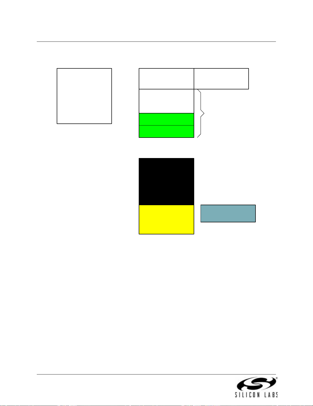
C8051F340/1/2/3/4/5/6/7/8/9/A/B/C/D
PROGRAM/DATA MEMORY
(FLASH)
(Direct and Indirect
Addressing)
0x00
0x7F
Upper 128 RAM
(Indirect Addressing
Only)
0x80
0xFF
Special Function
Register's
(Direct Addressing Only)
DATA MEMORY (RAM)
General Purpose
Registers
0x1F
0x20
0x2F
Bit Addressable
Lower 128 RAM
(Direct and Indirect
Addressing)
0x30
INTERNAL DATA ADDRESS SPACE
EXTERNAL DATA ADDRESS SPACE
XRAM - 2048 Bytes
(Accessable using MOVX
instruction)
0x0000
0x07FF
Off-Chip XRAM
(Available only on devices
with EMIF)
0x0400
0xFFFF
FLASH
(In-System
Programmable in 512
Byte Sectors)
0x0000
0x7FFF
USB FIFOs
1024 Bytes
0x07FF
0x0800
9.2.1. Program Memory
The CIP-51 core has a 64k-byte program memory space. The C8051F34x implements 64k or 32k bytes of
this program memory space as in-system, re-programmable Flash memory. Note that on the 64k versions
of the C8051F34x, addresses above 0xFBFF are reserved.
Program memory is normally assumed to be read-only.
by setting the Program Store Write Enable bit (PSCTL.0) and using the MOVX instruction. This feature provides a mechanism for the CIP-51 to update program code and use the program memory space for
non-volatile dat
80 Rev. 1.3
Figure 9.3. On-Chip Memory Map for 32 kB Devices
a storage. Refer to Section “12. Flash Memory” on page 107 for further details.
However , th e CIP-51 can wr ite to pro gram m emory
Page 81

C8051F340/1/2/3/4/5/6/7/8/9/A/B/C/D
9.2.2. Data Memory
The CIP-51 includes 256 of internal RAM mapped into the data memory space from 0x00 through 0xFF.
The lower 128 bytes of data memory are used for general purpose registers and scratch pad memory.
r direct or indirect addressing may be used to access the lower 128 bytes of data memory. Locations
Eithe
x00 through 0x1F are addressable as four banks of general purpose registers, each bank consisting of
0
eight byte-wide registers. The next 16 bytes, locations 0x20 through 0x2F, may either be addressed as
tes or as 128 bit locations accessible with the direct addressing mode.
by
The upper 128 bytes of data memory are accessible only by i ndir
same address space as the Special Function Registers (SFR) but is physically separate from the SFR
space. The addressing mode used by an instruction when accessing locations above 0x7F determines
whether the CPU accesses the upper 128 bytes of data memory space or the SFRs. In
direct addressing will access the SFR space. Instructions using indirect addressing above 0x7F access the
upper 128 bytes of data memory. Figure 9.2 illustrates the data memory organization
ect addressing. This region occupies the
structions that use
of the CIP-51.
9.2.3. General Purpose Registers
The lower 32 bytes of data memory, locations 0x00 through 0x1F, may be addressed as four banks of general-purpose registers. Each bank consists of eight b
one of these banks may be enabled at a time. Two bits in the program st atus wo rd , RS0 (PSW.3) and RS1
(PSW.4), select the active register bank (see description of the PSW in SFR Definition 9.4). This allows
fast context switching when entering subroutines and inte
use registers R0 and R1 as index registers.
yte-wide registers designated R0 through R7. Only
rrupt service routines. Indirect addressing modes
9.2.4. Bit Addressable Locations
In addition to direct access to data memory or ganize d as bytes, the sixteen d ata memory locations at 0x20
through 0x2F are also accessible as 128 individually addressable bits. Each bit has a bit address from
00 to 0x7F. Bit 0 of the byte at 0x20 has bit address 0x00 while bit7 of the by te at 0x20 has b it address
0x
x07. Bit 7 of the byte at 0x2F has bit address 0x7F. A bit access is distinguished from a full byte access by
0
the type of instruction used (bit source or destination operands as opposed to a byte source or destination).
The MCS-51™ assembly language allows an alternate no
XX is the byte address and B is the bit position within the byte. For example, the instruction:
tation for bit addressing of the form XX.B where
MOV C, 22h.3
moves the Boolean value at 0x13 (bit 3 of the byte at location 0x22) into the Carry flag.
9.2.5. Stack
A programmer's stack can be located anywhe re in the 256-byte data memory. The stack area is designated using the Stack Pointer (SP, 0x81) SFR.
pushed on the stack is placed at SP+1 and then SP is incremented. A reset initializes the stack pointer to
location 0x07. Therefore, the fir st value pushed on the stack is placed at location 0x08, which is also the
first register (R0) of registe r bank 1. Th us, if more than one register bank is to be used, the SP should be
initialized to a location in the data memory not being used for data storage. The stack de pth can exte nd up
to 256 bytes.
The SP will point to the last location used. The next value
Rev. 1.3 81
Page 82
C8051F340/1/2/3/4/5/6/7/8/9/A/B/C/D
Table 9.2. Special Function Register (SFR) Memory Map
F8 SPI0CN PCA0L PCA0H PCA0CPL0 PCA0CPH0 PCA0CPL4 PCA0CPH4 VDM0CN
F0
B P0MDIN P1MDIN P2MDIN P3MDIN P4MDIN EIP1 EIP2
E8
ADC0CN PCA0CPL1 PCA0CPH1 PCA0CPL2 PCA0CPH2 PCA0CPL3 PCA0CPH3 RSTSRC
E0
ACC XBR0 XBR1 XBR2 IT01CF SMOD1 E IE1 EIE2
D8
PCA0CN PCA0MD PCA0CPM0 PCA0CPM1 PCA0CPM2 PCA0CPM3 PCA0CPM4 P3SKIP
D0
PSW REF0CN SCON1 SBUF1 P0SKIP P1SKIP P2SKIP USB0XCN
C8
TMR2CN REG0CN TMR2RLL TMR2RLH TMR2L TMR2H - -
C0
SMB0CN SMB0CF SMB0DAT ADC0GTL ADC0GTH ADC0LTL ADC0LTH P4
B8
IP CLKMUL AMX0N AMX0P ADC0CF ADC0L ADC0H -
B0
P3 OSCXCN OSCICN OSCICL SBRLL1 SBRLH1 FLSCL FLKEY
A8
IE CLKSEL EMI0CN - SBCON1 - P4MDOUT PFE0CN
A0
P2 SPI0CFG SPI0CKR SPI0DAT P0MDOUT P1MDOUT P2MDOUT P3MDOUT
98
SCON0 SBUF0 CPT1CN CPT0CN CPT1MD CPT0MD CPT1MX CPT0MX
90
P1 TMR3CN TMR3RLL TMR3RLH TMR3L TMR3H USB0ADR USB0DAT
88
TCON TMOD TL0 TL1 TH0 TH1 CKCON PSCTL
80
P0 SP DPL DPH EMI0TC EMI0CF OSCLCN PCON
0(8) 1(9) 2(A) 3(B) 4(C) 5(D) 6(E) 7(F)
(bit addressable)
9.2.6. Special Function Registers
The direct-access data memory locations from 0x80 to 0xFF constitute the special function registers
(SFRs). The SFRs provide control and data exchange with the CIP-51's resources and peripherals. The
CIP-51 duplicates the SFRs found in a typical 8051 implementation as well as implementing additional
SFRs used to configure and access the sub-systems unique to the MCU. This allows the addition of new
functionality while retaining compatibility with the MCS-51™ instruction set. Table 9.2 list
mented in the CIP-51 System Controller.
s the SFRs imple-
The SFR registers are accessed anyt ime the dire ct addr
from 0x80 to 0xFF. SFRs with addresses ending in 0x0 or 0x8 (e.g. P0, TCON, SCON0, IE, etc.) are
bit-addressable as well as byte-addressable. All other SFRs are byte-addressable only. Unoccupied
addresses in the SFR space are reserved for future use. Accessing these areas will have an indeterminate
effect and should be avoided. Refer to the cor responding p a ges of the dat asheet, as indicated in Table 9.3,
for a detailed description of each register.
essing mode is used to access memory locations
82 Rev. 1.3
Page 83

C8051F340/1/2/3/4/5/6/7/8/9/A/B/C/D
Table 9.3. Special Function Registers
SFRs are listed in alphabetical order. All undefined SFR locations are reserved.
Register Address Description Page
ACC 0xE0 Accumulator 87
ADC0CF 0xBC ADC0 Configuration 50
ADC0CN 0xE8 ADC0 Control 51
ADC0GTH 0xC4 ADC0 Gr ea te r- Th a n Co mpare High 52
ADC0GTL 0xC3 ADC0 Greater-Th a n Co mpare Low 52
ADC0H 0xBE ADC0 High 50
ADC0L 0xBD ADC0 Low 50
ADC0LTH 0xC6 ADC0 Less-Than Compare Word High 53
ADC0LTL 0xC5 ADC0 Less-Than Compare Word Low 53
AMX0N 0xBA AMUX0 Negative Channel Select 49
AMX0P 0xBB AMUX0 Positive Channel Select 48
B 0xF0 B Register 88
CKCON 0x8E Clock Control 241
CLKMUL 0xB9 Clock Multiplier 138
CLKSEL 0xA9 Clock Select 140
CPT0CN 0x9B Comparator0 Control 62
CPT0MD 0x9D Comparator0 Mode Selection 64
CPT0MX 0x9F Comparator0 MUX Selection 63
CPT1CN 0x9A Comparator1 Control 65
CPT1MD 0x9C Comparator1 Mode Selection 67
CPT1MX 0x9E Comparator1 MUX Selection 66
DPH 0x83 Data Pointer High 86
DPL 0x82 Data Pointer Low 86
EIE1 0xE6 Extended Interrupt Enable 1 93
EIE2 0xE7 Extended Interrupt Enable 2 95
EIP1 0xF6 Extended Interrupt Priority 1 94
EIP2 0xF7 Extended Interrupt Priority 2 95
EMI0CN 0xAA External Memory Interface Control 117
EMI0CF 0x85 External Memory Interface Configuration 118
EMI0TC 0x84 External Memory Interface Timing 123
FLKEY 0xB7 Flash Lock and Key 112
FLSCL 0xB6 Flash Scale 113
IE 0xA8 Interrupt Enable 91
IP
IT01CF 0xE4 INT0/INT1 Configuration 96
OSCICL 0xB3 Internal Oscillator Calibration 133
OSCICN 0xB2 Internal Oscillator Control 132
OSCLCN 0x86 Internal Low-Frequency
OSCXCN 0xB1 External Oscillator Control 137
P0 0x80 Port 0 Latch 150
P0MDIN 0xF1 Port 0 Input Mo de Con fig ur at ion 150
P0MDOUT 0xA4 Port 0 Output Mode Configuration 151
P0SKIP 0xD4 Port 0 Skip 151
P1 0x90 Port 1 Latch 152
0xB8 Interrupt Priority 92
Oscillator Control 134
Rev. 1.3 83
Page 84

C8051F340/1/2/3/4/5/6/7/8/9/A/B/C/D
Table 9.3. Special Function Registers (Continued)
SFRs are listed in alphabetical order. All undefined SFR locations are reserved.
Register Address Description Page
P1MDIN 0xF2 Port 1 Input Mo de Con fig ur at ion 152
P1MDOUT 0xA5 Port 1 Output Mode Configuration 152
P1SKIP 0xD5 Port 1 Skip 153
P2 0xA0 Port 2 Latch 153
P2MDIN 0xF3 Port 2 Input Mo de Con fig ur at ion 153
P2MDOUT 0xA6 Port 2 Output Mode Configuration 154
P2SKIP 0xD6 Port 2 Skip 154
P3 0xB0 Port 3 Latch 155
P3MDIN 0xF4 Port 3 Input Mo de Con fig ur at ion 155
P3MDOUT 0xA7 Port 3 Output Mode Configuration 155
P3SKIP 0xDF Port 3Skip 156
P4 0xC7 Port 4 Latch 156
P4MDIN 0xF5 Port 4 Input Mo de Con fig ur at ion 157
P4MDOUT 0xAE Port 4 Output Mode Configuration 157
PCA0CN 0xD8 PCA Control 266
PCA0CPH0 0xFC PCA Capture 0 High 270
PCA0CPH1 0xEA PCA Capture 1 High 270
PCA0CPH2 0xEC PCA Capture 2 High 270
PCA0CPH3 0xEE PCA Capture 3High 270
PCA0CPH4 0xFE PCA Capture 4 High 270
PCA0CPL0 0xFB PCA Capture 0 Low 269
PCA0CPL1 0xE9 PCA Capture 1 Low 269
PCA0CPL2 0xEB PCA Capture 2 Lo w 269
PCA0CPL3 0xED PCA Capture 3 Low 269
PCA0CPL4 0xFD PCA Captur e 4 Lo w 269
PCA0CPM0 0xDA PCA Module 0 Mode Register 268
PCA0CPM1 0xDB PCA Module 1 Mode Register 268
PCA0CPM2 0xDC PCA Module 2 Mode Register 268
PCA0CPM3 0xDD PCA Module 3 Mode Register 268
PCA0CPM4 0xDE PCA Module 4 Mode Register 268
PCA0H 0xFA PCA Counter High 269
PCA0L 0xF9 PCA Counter Low 269
PCA0MD 0xD9 PCA Mode 267
PCON 0x87 Power Control
PFE0CN 0xAF Prefetch Engine Control 99
PSCTL 0x8F Program Store R/W Control 112
PSW 0xD0 Program Status Word 87
REF0CN 0xD1 Voltage Reference Control 58
REG0CN 0xC9 Voltage Regulator Control 72
RSTSRC 0xEF Reset Source Configuration/Status 105
SBCON1 0xAC UART1 Baud Rate Generator Control 220
SBRLH1 0xB5 UART1 Baud Rate Generator High 221
SBRLL1 0xB4 UART1 Baud Rate Generator Low 221
SBUF1 0xD3 UART1 Data Buffer 220
SCON1 0xD2 UART1 Control 218
98
84 Rev. 1.3
Page 85

C8051F340/1/2/3/4/5/6/7/8/9/A/B/C/D
Table 9.3. Special Function Registers (Continued)
SFRs are listed in alphabetical order. All undefined SFR locations are reserved.
Register Address Description Page
SBUF0 0x99 UART0 Data Buffer 211
SCON0 0x98 UART0 Control 210
SMB0CF 0xC1 SMBus Configuration 194
SMB0CN 0xC0 SMBus Control 196
SMB0DAT 0xC2 SMBus Data 198
SMOD1 0xE5 UART1 Mode 219
SP 0x81 Stack Pointer 86
SPI0CFG 0xA1 SPI Configuration 229
SPI0CKR 0xA2 SPI Clock Rate Control 231
SPI0CN 0xF8 SPI Control 230
SPI0DAT 0xA3 SPI Data 231
TCON 0x88 Timer/Counter Control 239
TH0 0x8C Timer/Counter 0 High 242
TH1 0x8D Timer/Counter 1 High 242
TL0 0x8A Timer/Counter 0 Low 242
TL1 0x8B Timer/Counter 1 Low 242
TMOD 0x89 Timer/Counter Mode 240
TMR2CN 0xC8 T imer/Counter 2 Control 247
TMR2H 0xCD Timer/Counter 2 High 248
TMR2L 0xCC Timer/Counter 2 Low 248
TMR2RLH 0xCB Timer/Counter 2 Reload High 248
TMR2RLL 0xCA Timer/Counter 2 Reload Low 248
TMR3CN 0x91 Timer/Counter 3Control 253
TMR3H 0x95 Timer/Counter 3 High 254
TMR3L 0x94 Timer/Counter 3Low 254
TMR3RLH 0x93 Timer/Counter 3 Reload High 254
TMR3RLL 0x92 Timer/Counter 3 Reload Low 254
V
VDM0CN 0xFF
USB0ADR 0x96 USB0 Indirect Address Register 163
USB0DAT 0x97 USB0 Data Register 164
USB0XCN 0xD7 USB0 Transceiver Control 161
XBR0 0xE1 Port I/O Crossbar Control 0 148
XBR1 0xE2 Port I/O Crossbar Control 1 149
XBR2
All Other Addresses Reserved
0xE3 Port I/O Crossbar Control 2 149
Monitor Control
DD
102
Rev. 1.3 85
Page 86
C8051F340/1/2/3/4/5/6/7/8/9/A/B/C/D
Bits7–0: DPL: Data Pointer Low.
The DPL register is the low byte of the 16-bit DPTR. DPTR is used to access indirectly
addressed memory.
R/W R/W R/W R/W R/W R/W R/W R/W R eset Value
00000000
Bit7 Bit6 Bit5 Bit4 Bit3 Bit2 Bit1 Bit0 SFR Address:
0x82
Bits7–0: DPH: Data Pointer High.
The DPH register is the high byte of the 16-bit DPTR. DPTR is used to access indirectly
addressed memory.
R/W R/W R/W R/W R/W R/W R/W R/W Reset Value
00000000
Bit7 Bit6 Bit5 Bit4 Bit3 Bit2 Bit1 Bit0 SFR Address:
0x83
Bits7–0: SP: Stack Pointer.
The Stack Pointer holds the location of the top of the stack. The stack pointer is incremented
before every PUSH operation. The SP register defaults to 0x07 afte r reset.
R/W R/W R/W R/W R/W R/W R/W R/W Reset Value
00000111
Bit7 Bit6 Bit5 Bit4 Bit3 Bit2 Bit1 Bit0 SFR Address:
0x81
9.2.7. Register Descriptions
Following are descriptions of SFRs related to the operation of the CIP-51 System Controller . Reserved bit s
should not be set to logic l. Future product versions may use these bits to implement new features in which
the reset value of the bit will be logic 0, selecting the feature's default st
case
the remaining SFRs are included in the sections of the datasheet associated with their corresponding system function.
SFR Definition 9.1. DPL: Data Pointer Low Byte
ate. Detailed descriptions of
SFR Definition 9.2. DPH: Data Pointer High Byte
SFR Definition 9.3. SP: Stack Pointer
86 Rev. 1.3
Page 87

C8051F340/1/2/3/4/5/6/7/8/9/A/B/C/D
Bit7: CY: Carry Flag.
This bit is set when the last arithmetic operation resulted in a carry (addition) or a borrow
(subtraction). It is cleared to logic 0 by all other arithmetic operations.
Bit6: AC: Auxiliary Carry Flag
This bit is set when the last arithmetic operation resulted in a carry into (addition) or a borrow
from (subtraction) the high order nibble. It is cleared to logic 0 by a ll other arithmetic oper ations.
Bit5: F0: User Flag 0.
This is a bit-addressable, general purpose flag for use under software contr ol.
Bits4–3: RS1–RS0: Register Bank Select.
These bits select which register bank is used during register accesses.
Bit2: OV: Overflow Flag.
This bit is set to 1 under the following circumstances:
• An ADD, ADDC, or SUBB instruction causes a sign-change overflow.
• A MUL instruction results in an overflow (result is greater than 255) .
• A DIV instruction causes a divide-by-zero condition.
The OV bit is cleared to 0 by the ADD, ADDC, SUBB, MUL, and DIV instructions in all other
cases.
Bit1: F1: User Flag 1.
This is a bit-addressable, general purpose flag for use under software contr ol.
Bit0: PARITY: Parity Flag.
This bit is set to logic 1 if the sum of the eight bits in the accumulator is odd and cleared if the
sum is even.
R/W R/W R/W R/W R/W R/W R/W R Reset Value
CY AC F0 RS1 RS0 OV F1 PARITY 00000000
Bit7 Bit6 Bit5 Bit4 Bit3 Bit2 Bit1 Bit0 SFR Address:
(bit addressable)
0xD0
RS1 RS0 Register Bank Address
0 0 0 0x00 - 0x07
0 1 1 0x08 - 0x0F
1 0 2 0x10 - 0x17
1 1 3 0x18 - 0x1F
Bits7–0: ACC: Accumulator.
This register is the accumulator for arithmetic operations.
R/W R/W R/W R/W R/W R/W R/W R/W Reset Value
ACC.7 ACC.6 ACC.5 ACC.4 ACC.3 ACC.2 ACC.1 ACC.0 00000000
Bit7 Bit6 Bit5 Bit4 Bit3 Bit2 Bit1 Bit0 SFR Address:
(bit addressable)
0xE0
SFR Definition 9.4. PSW: Program Status Word
SFR Definition 9.5. ACC: Accumulator
Rev. 1.3 87
Page 88

C8051F340/1/2/3/4/5/6/7/8/9/A/B/C/D
Bits7–0: B: B Register.
This register serves as a second accumulator for certain arithmetic operations.
R/W R/W R/W R/W R/W R/W R/W R/W Reset Value
B.7 B.6 B.5 B.4 B.3 B.2 B.1 B.0 00000000
Bit7 Bit6 Bit5 Bit4 Bit3 Bit2 Bit1 Bit0 SFR Address:
(bit addressable)
0xF0
SFR Definition 9.6. B: B Register
9.3. Interrupt Handler
The CIP-51 includes an extended interrupt system supporting multiple interrupt sources with two priority
levels. The allocation of interrupt sources between on-chip peripherals and external inputs pins varies
according to the specific version of the device. Each interrupt source has one or more associated interrupt-pending flag(s) located in an SFR. When a periph
tion, the associated interrupt-pending flag
is set to logic 1.
eral or external source meets a valid interrupt condi-
If interrupts are enabled for the source, an interrupt request
set. As soon as execution of the current instruction is complete, the CPU generates an LCALL to a predetermined address to begin execution of an interrupt service ro
instruction, which returns program execution to the next instruction that would have been executed if the
interrupt request had not occurred. If interrupts are not en abled, the inter rupt-pending flag is ignored by the
hardware and program execution continues as normal. (The interrupt-pending flag is set to logic 1 regardless of the interrupt's enable/disable state.)
Each interrupt source can be individually enabled or di
enable bit in an SFR (IE-EIE2). However, interrupts must first be globally enabled by setting the EA bit
(IE.7) to logic 1 before the individual interrupt enables are re cogn
all interrupt sources regardless of the individual interrupt-enable settings.
Some interrupt-pending flags are automatically cleared
However, most are not cle ared by the hardwar e and must be cleared by so f tware befo re returning from the
ISR. If an interrupt-pending flag remains set after the CPU completes the return-from-interrupt (RETI)
instruction, a new interrupt request will be generated immediately and the CPU will re-enter the ISR after
the completion of the next instruction.
is generated when the interrupt-pending flag is
utine (ISR). Each ISR must end with an RETI
sabled through the use of an associated interrupt
ized. Setting the EA bit to logic 0 disables
by the hardware when the CPU vectors to the ISR.
9.3.1. MCU Interrupt Sources and Vectors
The MCU supports multiple interrupt sources. Software can simulate an interrupt by setting any interrupt-pending flag to logic 1. If interrupts are enabled for the flag,
the CPU will vector to the ISR address associated with the interrupt-pending flag. MCU interrupt sources,
associated vector addresses, priority order and control bits are summarized in Table 9.4 on page 90. Refer
to the datasheet section associated with a particular on-chip peripheral for information regarding valid
terrupt conditions for the peripheral and the behavior of its interrupt-pending flag(s).
in
an interrupt request will be generated and
9.3.2. External Interrupts
The INT0 and INT1 external interrupt sources are configurable as active high or low, edge or level sensitive. The IN0PL (
active low; the IT0 and IT1 bits in TCON (Section “21.1. Timer 0 and Timer 1” on page 235) select level
or edge sensitive. The following table list
88 Rev. 1.3
INT0 Polarity) and IN1PL (INT1 Polarity) bits in the IT01CF register select active high or
s the possible configurations.
Page 89

C8051F340/1/2/3/4/5/6/7/8/9/A/B/C/D
IT0 IN0PL INT0 Interrupt IT1 IN1PL INT1 Interrupt
10
11Active high, edge sensitive 11Active high, edge sensitive
00Active low, level sensitive 00Active low, level sensitive
01Active high, level sensitive 01Active high, level sensitive
INT0 and INT1 are assigned to Port pins as defined in the IT01CF reg ister (see SFR Definition 9.13). Note
INT0 and INT0 Port pin assignments are independent of any Crossbar assignments. INT0 and INT1
that
will monitor their assigned Port pins without disturbing the peripheral that was assigned the Port pin via the
Crossbar . To assign a Port pin only to
This is accomplished by setting the associated bit in register XBR0 (se e Section “15.1. Priority Crossbar
Decoder” on page 144 for complete details on configuring the Crossbar
external interrupt pin should be skipped in the crossbar and configured as open-drain with the pin latch set
to '1'.
Active low, edge sensitive 10Active low, edge sensitive
INT0 and/or INT1, configure the Crossbar to skip the selected pin(s).
). In the typical configuration, the
IE0 (TCON.1) and IE1 (TCON.3) serve as the in
rupts, respectively. If an
interrupt-pending flag is automatically cleared by the hardware when the CPU vectors to the ISR. When
configured as level sensitive, the interrupt-pending flag remains logic 1 while the input is active as defined
by the corresponding polarity bit (IN0PL or IN1PL); the flag remains logic 0 while the input is inactive. The
external interrupt source must hold the input active until the inter rupt request is recognized. It must then
deactivate the interrupt request before execution of the ISR completes or another interrupt request will be
generated.
INT0 or INT1 external interrupt is configured as edge-sensitive, the correspondin g
terrupt-pending flags for the INT0 and INT1 external inter-
9.3.3. Interrupt Priorities
Each interrupt source can be individually programmed to one of two priority levels: low or high. A low priority interrupt service routine can be preempted
preempted. Each interrupt has an associated interrupt priority bit in an SFR (IP or EIP2) used to configure
its priority level. Low priority is the default. If two interrupts are re cognized simult aneously, the interrupt with
the higher priority is serviced first. If both interrupts have the same priority level, a fixed priority order is
used to arbitrate, given in Table 9.4.
by a high priority interrupt. A high priority interrupt cannot be
9.3.4. Interrupt Latency
Interrupt response time depends on the state of the CPU whe n the in terr upt occur s. Pending inter rupts are
sampled and priority decoded each system clock cycle. Therefore, the fastest possible response time is 6
system clock cycles: 1 clock cycle to detect the interrupt and 5 clock cycles to complete the LCALL to the
If an interrupt is pending when a RETI is executed, a single instruction is executed before an LCALL
ISR.
is made to service the pending interrup t. Th eref ore, the maxim um r espo nse time for an inter rupt (when no
other interrupt is currently being serviced or the new interrupt is of greater priority) occurs when the CPU is
performing an RETI instruction followed by a DIV as the next instruction. In this case, the response time is
20 system clock cycles: 1 clock cycle to detect the interrupt, 6 clock cycles to execute the RETI, 8 clock
les to complete the DIV instruction and 5 clock cycles to execute the LCALL to the ISR. If the CPU is
cyc
ecuting an ISR for an interrupt with equal or higher priority , the new interrupt will not be serviced until the
ex
current ISR completes, including the RETI and following instruction.
Note that the CPU is stalled during Flash write/e
Section “13.2. Accessing USB FIFO Sp ac e” on page 115). Interrupt service latency
interrupts occurring while the CPU is st
standard interrupt service procedure (as described above) and the amount of time the CPU is stalled.
alled. The latency for these situations will be determined by the
rase operations and USB FIFO MOVX accesses (see
will be increased for
Rev. 1.3 89
Page 90

C8051F340/1/2/3/4/5/6/7/8/9/A/B/C/D
Table 9.4. Interrupt Summary
Interrupt Source
Reset 0x0000 Top None N/A N/A
External Interrupt 0
INT0)
(
Timer 0 Overflow 0x000B 1 TF0 (TCON.5) Y Y ET0 (IE.1) PT0 (IP.1)
External Interrupt 1
INT1)
(
Timer 1 Overflow 0x001B 3 TF1 (TCON.7) Y Y ET1 (IE.3) PT1 (IP.3)
UART0 0x0023 4
Timer 2 Overflow 0x002B 5
SPI0 0x0033 6
SMB0 0x003B 7 SI (SMB0CN.0) Y N
USB0 0x0043 8 Special N N
ADC0 Window
Comp
are
ADC0 Conversion
Complete
Programmable Counter
Array
Comparator0 0x0063 12
Comparator1 0x006B 13
Timer 3 Overflow 0x0073 14
VBUS Level 0x007B 15 N/A N/A N/A
UART1 0x0083 16
Interrupt
Vector
0x0003 0 IE0 (TCON.1) Y Y EX0 (IE.0) PX0 (IP.0)
0x0013 2 IE1 (TCON.3) Y Y EX1 (IE.2) PX1 (IP.2)
0x004B 9
0x0053 10 AD0INT (ADC0CN.5) Y N
0x005B 11
Priority
Order
Pending Flag
RI0 (SCON0.0)
TI0 (SCON0.1)
TF2H (TMR2CN.7)
TF2L (TMR2CN.6)
SPIF (SPI0CN.7)
WCOL (SPI0CN.6)
MODF (SPI0CN.5)
RXOVRN (SPI0CN.4)
AD0WINT
(ADC0CN
CF (PCA0CN.7)
CCFn (PCA0CN.n)
CP0FIF (CPT0CN.4)
P0RIF (CPT0CN.5)
C
CP1FIF (CPT1CN.4)
P1RIF (CPT1CN.5)
C
TF3H (TMR3CN.7)
TF3L (TMR3CN.6)
RI1 (SCON1.0)
TI1 (SCON1.1)
.3)
Enable
Flag
Cleared by HW?
Bit addressable?
Always
abled
En
Y N ES0 (IE.4) PS0 (IP.4)
Y N ET2 (IE.5) PT2 (IP.5)
Y N
Y N
Y N
N N
N N
N N
N N
ESPI0
)
(IE.6
ESMB0
(EIE1.0)
EUSB0
(EIE1.1)
EWADC0
(EIE1.2)
EADC0
(EIE1.3)
EPCA0
(EIE1.4)
ECP0
(EIE1.5)
ECP1
(EIE1.6)
ET3
(EIE1.7)
EVBUS
(EIE2.0)
ES1
(EIE2.1)
Priority
Control
Always
Highest
PSPI0
(IP.6)
PSMB0
.0)
(EIP1
PUSB0
.1)
(EIP1
PWADC0
.2)
(EIP1
PADC0
.3)
(EIP1
PPCA0
.4)
(EIP1
PCP0
.5)
(EIP1
PCP1
.6)
(EIP1
PT3
.7)
(EIP1
PVBUS
.0)
(EIP2
PS1
.1)
(EIP2
9.3.5. Interrupt Register Descriptions
The SFRs used to enable the interrupt sources and set their pr iority le vel are de scri bed below. Refer to the
datasheet section associated with a particular on-chip peripheral for information regarding valid interrup t
conditions for the peripheral and the behavio r of its interrupt-p en ding flag (s) .
90 Rev. 1.3
Page 91

C8051F340/1/2/3/4/5/6/7/8/9/A/B/C/D
Bit7: EA: Enable All Interrupts.
This bit globally enables/disables all interrupts. It overrides the individual interrupt mask settings.
0: Disable all interrupt sources.
1: Enable each interrupt according to its individual mask setting.
Bit6: ESPI0: Enable Serial Peripheral Interface (SPI0) Interrupt.
This bit sets the masking of the SPI0 interrupts.
0: Disable all SPI0 interrupts.
1: Enable interrupt requests generated by SPI0.
Bit5: ET2: Enable Timer 2 Interrupt.
This bit sets the masking of the Timer 2 interrupt.
0: Disable Timer 2 interrupt.
1: Enable interrupt requests generated by the TF2L or TF2H flags.
Bit4: ES0: Enable UART0 Interrupt.
This bit sets the masking of the UART0 interrupt.
0: Disable UART0 interrupt.
1: Enable UART0 interrupt.
Bit3: ET1: Enable Timer 1 Interrupt.
This bit sets the masking of the Timer 1 interrupt.
0: Disable all Timer 1 interrupt.
1: Enable interrupt requests generated by the TF1 flag.
Bit2: EX1: Enable External Interrupt 1.
This bit sets the masking of External Interrupt 1.
0: Disable external interrupt 1.
1: Enable interrupt requests generated by the INT1
input.
Bit1: ET0: Enable Timer 0 Interrupt.
This bit sets the masking of the Timer 0 interrupt.
0: Disable all Timer 0 interrupt.
1: Enable interrupt requests generated by the TF0 flag.
Bit0: EX0: Enable External Interrupt 0.
This bit sets the masking of External Interrupt 0.
0: Disable external interrupt 0.
1: Enable interrupt requests generated by the INT0
input.
R/W R/W R/W R/W R/W R/W R/W R/W Reset Value
EA ESPI0 ET2 ES0 ET1 EX1 ET0 EX0 00000000
Bit7 Bit6 Bit5 Bit4 Bit3 Bit2 Bit1 Bit0 SFR Address:
(bit addressable)
0xA8
SFR Definition 9.7. IE: Interrupt Enable
Rev. 1.3 91
Page 92

C8051F340/1/2/3/4/5/6/7/8/9/A/B/C/D
Bit7: UNUSED. Read = 1, Write = don't care.
Bit6: PSPI0: Serial Peripheral Interface (SPI0) Interrupt Priority Control.
This bit sets the priority of the SPI0 interrupt.
0: SPI0 interrupt set to low priority level.
1: SPI0 interrupt set to high priority level.
Bit5: PT2: Timer 2 Interrupt Priority Control.
This bit sets the priority of the Timer 2 interrupt.
0: Timer 2 interrupt set to low priority level.
1: Timer 2 interrupts set to high priority level.
Bit4: PS0: UART0 Interrupt Priority Control.
This bit sets the priority of the UART0 interrupt.
0: UART0 interrupt set to low priority level.
1: UART0 interrupts set to high priority level.
Bit3: PT1: Timer 1 Interrupt Priority Control.
This bit sets the priority of the Timer 1 interrupt.
0: Timer 1 interrupt set to low priority level.
1: Timer 1 interrupts set to high priority level.
Bit2: PX1: External Interrupt 1 Priority Control.
This bit sets the priority of the External Interrupt 1 interrupt.
0: External Interrupt 1 set to low priority level.
1: External Interrupt 1 set to high priority level.
Bit1: PT0: Timer 0 Interrupt Priority Control.
This bit sets the priority of the Timer 0 interrupt.
0: Timer 0 interrupt set to low priority level.
1: Timer 0 interrupt set to high priority level.
Bit0: PX0: External Interrupt 0 Priority Control.
This bit sets the priority of the External Interrupt 0 interrupt.
0: External Interrupt 0 set to low priority level.
1: External Interrupt 0 set to high priority level.
R/W R/W R/W R/W R/W R/W R/W R/W Reset Value
- PSPI0 PT2 PS0 PT1 PX1 PT0 PX0 10000000
Bit7 Bit6 Bit5 Bit4 Bit3 Bit2 Bit1 Bit0 SFR Address:
(bit addressable)
0xB8
SFR Definition 9.8. IP: Interrupt Priority
92 Rev. 1.3
Page 93

C8051F340/1/2/3/4/5/6/7/8/9/A/B/C/D
Bit7: ET3: Enable Timer 3 Interrupt.
This bit sets the masking of the Timer 3 interrupt.
0: Disable Timer 3 interrupts.
1: Enable interrupt requests generated by the TF3L or TF3H flags.
Bit6: ECP1: Enable Comparator1 (CP1) Interrupt.
This bit sets the masking of the CP1 interrupt.
0: Disable CP1 interrupts.
1: Enable interrupt requests generated by the CP1RIF or CP1FIF flags.
Bit5: ECP0: Enable Comparator0 (CP0) Interrupt.
This bit sets the masking of the CP0 interrupt.
0: Disable CP0 interrupts.
1: Enable interrupt requests generated by the CP0RIF or CP0FIF flags.
Bit4: EPCA0: Enable Programmable Counter Array (PCA0) Interrupt.
This bit sets the masking of the PCA0 interrupts.
0: Disable all PCA0 interrupts.
1: Enable interrupt requests generated by PCA0.
Bit3: EADC0: Enable ADC0 Conversion Complete Interrupt.
This bit sets the masking of the ADC0 Conversion Complete interrupt.
0: Disable ADC0 Conversion Complete interrupt.
1: Enable interrupt requests generated by the AD0INT flag.
Bit2: EWADC0: Enable Window Comparison ADC0 Interrupt.
This bit sets the masking of ADC0 Window Comparison interrupt.
0: Disable ADC0 Window Comparison interrupt.
1: Enable interrupt requests generated by ADC0 Window Compare flag (AD0WINT).
Bit1: EUSB0: Enable USB0 Interrupt.
This bit sets the masking of the USB0 interrupt.
0: Disable all USB0 interrupts.
1: Enable interrupt requests generated by USB0.
Bit0: ESMB0: Enable SMBus (SMB0) Interrupt.
This bit sets the masking of the SMB0 interrupt.
0: Disable all SMB0 interrupts.
1: Enable interrupt requests generated by SMB0.
R/W R/W R/W R/W R/W R/W R/W R/W Reset Value
ET3 ECP1 ECP0 EPCA0 EADC0 EWADC0 EUSB0 ESMB0 00000000
Bit7 Bit6 Bit5 Bit4 Bit3 Bit2 Bit1 Bit0 SFR Address:
0xE6
SFR Definition 9.9. EIE1: Extended Interrupt Enable 1
Rev. 1.3 93
Page 94

C8051F340/1/2/3/4/5/6/7/8/9/A/B/C/D
Bit7: PT3: Timer 3 Interrupt Priority Control.
This bit sets the priority of the Timer 3 interrupt.
0: Timer 3 interrupts set to low priority level.
1: Timer 3 interrupts set to high priority level.
Bit6: PCP1: Comparator1 (CP1) Interrupt Priority Control.
This bit sets the priority of the CP1 interrupt.
0: CP1 interrupt set to low priority level.
1: CP1 interrupt set to high priority level.
Bit5: PCP0: Comparator0 (CP0) Interrupt Priority Control.
This bit sets the priority of the CP0 interrupt.
0: CP0 interrupt set to low priority level.
1: CP0 interrupt set to high priority level.
Bit4: PPCA0: Programmable Counter Array (PCA0) Interrupt Priority Control.
This bit sets the priority of the PCA0 interrupt.
0: PCA0 interrupt set to low priority level.
1: PCA0 interrupt set to high priority level.
Bit3: PADC0 ADC0 Conversion Complete Interrupt Priority Control.
This bit sets the priority of the ADC0 Conversion Complete interrupt.
0: ADC0 Conversion Complete interrupt set to low priority level.
1: ADC0 Conversion Complete interrupt set to high priority level.
Bit2: PWADC0: ADC0 Window Comparator Interrupt Priority Control.
This bit sets the priority of the ADC0 Window interrupt.
0: ADC0 Window interrupt set to low priority level.
1: ADC0 Window interrupt set to high priority level.
Bit1: PUSB0: USB0 Interrupt Priority Control.
This bit sets the priority of the USB0 interrupt.
0: USB0 interrupt set to low priority level.
1: USB0 interrupt set to high priority level.
Bit0: PSMB0: SMBus (SMB0) Interrupt Priority Control.
This bit sets the priority of the SMB0 interrupt.
0: SMB0 interrupt set to low priority level.
1: SMB0 interrupt set to high priority level.
R/W R/W R/W R/W R/W R/W R/W R/W R eset Value
PT3 PCP1 PCP0 PPCA0 PADC0 PWADC0 PUSB0 PSMB0 00000000
Bit7 Bit6 Bit5 Bit4 Bit3 Bit2 Bit1 Bit0 SFR Address:
0xF6
SFR Definition 9.10. EIP1: Extended Interrupt Priority 1
94 Rev. 1.3
Page 95

C8051F340/1/2/3/4/5/6/7/8/9/A/B/C/D
Bits7–2: UNUSED. Read = 000000b. Write = don’t care.
Bit1: ES1: Enable UART1 Interrupt.
This bit sets the masking of the UART1 interrupt.
0: Disable UART1 interrupt.
1: Enable UART1 interrupt.
Bit0: EVBUS: Enable VBUS Level Interrupt.
This bit sets the masking of the VBUS interrupt.
0: Disable all VBUS interrupts.
1: Enable interrupt requests generated by VBUS level sense.
R/W R/W R/W R/W R/W R/W R/W R/W Reset Value
- - - - - - ES1 EVBUS 00000000
Bit7 Bit6 Bit5 Bit4 Bit3 Bit2 Bit1 Bit0 SFR Address:
0xE7
Bits7–2: UNUSED. Read = 000000b. Write = don’t care.
Bit1: PS1: UART1 Interrupt Priority Control.
This bit sets the priority of the UART1 interrupt.
0: UART1 interrupt set to low priority level.
1: UART1 interrupts set to high priority level.
Bit0: PVBUS: VBUS Level Interrupt Priority Control.
This bit sets the priority of the VBUS interrupt.
0: VBUS interrupt set to low priority level.
1: VBUS interrupt set to high priority level.
R/W R/W R/W R/W R/W R/W R/W R/W Reset Value
- - - - - - PS1 PVBUS 00000000
Bit7 Bit6 Bit5 Bit4 Bit3 Bit2 Bit1 Bit0 SFR Address:
0xF7
SFR Definition 9.11. EIE2: Extended Interrupt Enable 2
SFR Definition 9.12. EIP2: Extended Interrupt Priority 2
Rev. 1.3 95
Page 96
C8051F340/1/2/3/4/5/6/7/8/9/A/B/C/D
Bit7: IN1PL: INT1 Polarity
0: INT1
input is active low.
1: INT1
input is active high.
Bits6–4: IN1SL2–0: INT1
Port Pin Selection Bits
These bits select which Port pin is assigned to INT1
. Note that this pin assignment is inde-
pendent of the Crossbar; INT1
will monitor the assigned Port pin without disturbing the
peripheral that has been assigned the Port pin via the Crossbar. The Crossbar will not
assign the Port pin to a peripheral if it is configure d to skip the selected pin (accomplished by
setting to ‘1’ the corresponding bit in register P0SKIP).
Bit3: IN0PL: INT0
Polarity
0: INT0
interrupt is active low.
1: INT0
interrupt is active high.
Bits2–0: INT0SL2–0: INT0
Port Pin Selection Bits
These bits select which Port pin is assigned to INT0
. Note that this pin assignment is inde-
pendent of the Crossbar. INT0
will monitor the assigned Port pin without disturbing the
peripheral that has been assigned the Port pin via the Crossbar. The Crossbar will not
assign the Port pin to a peripheral if it is configure d to skip the selected pin (accomplished by
setting to ‘1’ the corresponding bit in register P0SKIP).
R/W R/W R/W R/W R/W R/W R/W R/W Reset Value
IN1PL IN1SL2 IN1SL1 IN1SL0 IN0PL IN0SL2 IN0SL1 IN0SL0 00000001
Bit7 Bit6 Bit5 Bit4 Bit3 Bit2 Bit1 Bit0 SFR Address:
0xE4
Note: Refer to SFR Definition 21.1 for INT0/1 edge- or level-sensitive interrupt selection.
IN1SL2–0
INT1
Port Pin
000 P0.0
001 P0.1
010 P0.2
011 P0.3
100 P0.4
101 P0.5
110 P0.6
111 P0.7
IN0SL2–0 INT0
Port Pin
000 P0.0
001 P0.1
010 P0.2
011 P0.3
100 P0.4
101 P0.5
110 P0.6
111 P0.7
SFR Definition 9.13. IT01CF: INT0/INT1 Configuration
96 Rev. 1.3
Page 97

C8051F340/1/2/3/4/5/6/7/8/9/A/B/C/D
9.4. Power Management Modes
The CIP-51 core has two software programmable power management modes: Idle and Stop. Idle mode
halts the CPU while leaving the peripherals and clocks active. In Stop mode, the CPU is halted, all interrupts, are inactive, and the
the external oscillator is not affected). Since clocks are running in Idle mode, power consumption is dependent upon the system clock frequency and the number of p
Idle. Stop mode consumes the least power. Figure 1.15 describes the Power Control Register (PCON )
used to control the CIP-51's power management modes.
internal oscillator is stopped (analog peripherals remain in their selected states;
eripherals left in active mode before entering
Although the CIP-51 has Idle and Stop modes built in (
management of the entire MCU is better accomplished through system clock and individual peripheral
management. Each analog peripheral can be disabled when not in use and placed in low power mode.
Digital peripherals, such as timers or serial buses, draw little power when they are not in us e. Turning off
the oscillators lowers power consumption considerably; however a reset is required to restart the MCU.
The internal oscillator can be
Suspend mode, the internal
signal matches the polarity selected by the VBPOL bit in register REG0CN (SFR Definition 8.1).
placed in Suspend mode (see Section “14. Oscillators” on page 131). In
oscillator is stopped until a non-idle USB event is detected, or the VBUS input
as with any standard 8051 architecture), power
9.4.1. Idle Mode
Setting the Idle Mode Select bit (PCON.0) causes the CIP-51 to halt the CPU and enter Idle mode as soon
as the instruction that sets the bit completes execution. All internal registers and memory maintain their
original data. All analog and digital peripherals can remain active during Idle mode.
Idle mode is terminated when an enabled interrupt is asserted or a reset occurs. The assertion of an
enabled
operation. The pending interrupt will be serviced and the next instruction to be executed after the return
from interrupt (RETI) will be the instruction immediately following the one that set the Idle Mode Select bit.
If Idle mode is terminated by an internal or external reset, the CIP-51 performs a normal reset sequence
and begins program execution at address 0x0000.
If enabled, the Watchdog Timer (WDT) will eventually cause an
nate the Idle mode. This feature protects the system from an unintended per manent shutdown in the event
f an inadvertent write to the PCON register. If this behavior is not desired, the WDT may be disabled by
o
software prior to entering the Idle mode if the WDT was initially configured to allow this operation. This provides the opportunity for additional power savings, allow
nitely, waiting for an external stimulus to wake up the system. Refer to Section “11.6. PCA Watchdog
Timer Reset ” on page 103 for more information on the use and configuration of the WDT.
interrupt will cause the Idle Mode Selection bit (PCON.0) to be cleared and the CPU to resume
internal watchdog reset and thereby termi-
ing the system to remain in the Idle mode indefi-
9.4.2. Stop Mode
Setting the Stop Mode Select bit (PCON.1) causes the CIP-51 to enter Stop mode as soon as the instruction that sets the bit completes execution. In S
als are stopped; the state of
the external oscillator circuit) may be shut down individually prior to entering Stop Mode. Stop mode can
only be terminated by an internal or external reset. On reset, the CIP-51 performs the normal reset
sequence and begins program execution at address 0x0000.
If enabled, the Missing Clock Detector will cause
The Missing Clock Detector should be disabled if the CPU is to be put to in STOP mode for longer than the
MCD timeout of 100 µsec.
the external oscillator circuit is not affected. Each analog peripheral (including
top mode the internal oscillator, CPU, and all digita l peripher-
an internal reset and thereby terminate the Stop mode.
Rev. 1.3 97
Page 98

C8051F340/1/2/3/4/5/6/7/8/9/A/B/C/D
Bits7–2: GF5–GF0: General Purpose Flags 5–0.
These are general purpose flags for use under software control.
Bit1: STOP: Stop Mode Select.
Setting this bit will place the CIP-51 in Stop mode. This bit will always be read as 0.
1: CPU goes into Stop mode (internal oscillator stopped).
Bit0: IDLE: Idle Mode Select.
Setting this bit will place the CIP-51 in Idle mode. This bit will always be read as 0.
1: CPU goes into Idle mode. (Shuts off clock to CPU, but clock to Timers, Interrupts, Serial
Ports, and Analog Peripherals are still active.)
R/W R/W R/W R/W R/W R/W R/W R/W Reset Value
GF5 GF4 GF3 GF2 GF1 GF0 STOP IDLE 00000000
Bit7 Bit6 Bit5 Bit4 Bit3 Bit2 Bit1 Bit0 SFR Address:
0x87
SFR Definition 9.14. PCON: Power Control
98 Rev. 1.3
Page 99

C8051F340/1/2/3/4/5/6/7/8/9/A/B/C/D
Bits 7–6: Unused. Read = 00b; Write = Don’t Care
Bit 5: PFEN: Prefetch Enable.
This bit enables the prefetch engine.
0: Prefetch engine is disabled.
1: Prefetch engine is enabled.
Bits 4–1: Unused. Read = 0000b; Write = Don’t Care
Bit 0: FLBWE: FLASH Block Write Enable.
This bit allows block writes to FLASH memory from software.
0: Each byte of a software FLASH write is written individually.
1: FLASH bytes are written in groups of two.
R R R/W R R R R R/W Reset Value
PFEN FLBWE 00100000
Bit7 Bit6 Bit5 Bit4 Bit3 Bit2 Bit1 Bit0
SFR Address: 0xAF
10. Prefetch Engine
The 48 MHz versions of the C8051F34x family of devices incorporate a 2-byte prefetch engine. Because
the access time of the FLASH memory is 40 ns, and the minimum instruction time is roughly 20 ns, the
refetch engine is necessary for full-speed code exec ution. Instr uctions are re ad from FLASH m emory two
p
bytes at a time by the prefetc h engine, and given to the CIP-51 processor core to execute. When running
linear code (code without any jumps or branches), the prefetch engine allows instructions to be executed
at full speed. When a code branch occurs, the processor may be stalled for up to two clock cycles while the
next set of code bytes is retrieved from FLASH memory. The FLRT bit (FLSCL.4) determines how many
clock cycles are used to read each set of two code bytes from FLASH. When operating from a system
clock of 25 MHz or less, the FLRT bit should be set to ‘0’ so that the
cycle for each read. When operating with a system clock of greater than 25 MHz (up to 48 MHz), the FLRT
it should be set to ‘1’, so that each prefetch code read lasts for two clock cycles.
b
SFR Definition 10.1. PFE0CN: Prefetch Engine Control
prefetch engine takes only one clock
Rev. 1.3 99
Page 100
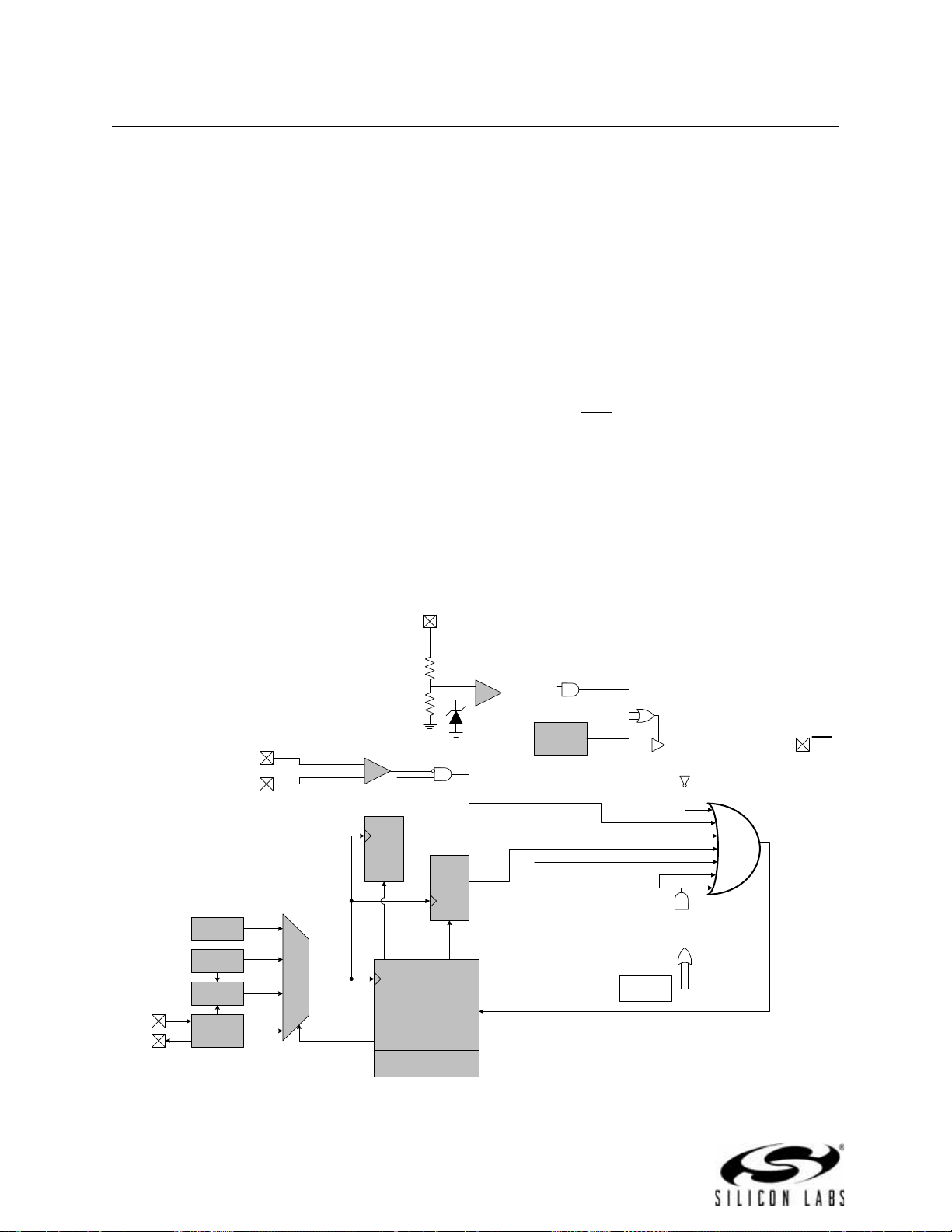
C8051F340/1/2/3/4/5/6/7/8/9/A/B/C/D
PCA
WDT
Missing
Clock
Detector
(oneshot)
Software Reset (SWRSF)
System Reset
Reset
Funnel
Px.x
Px.x
EN
System
Clock
CIP-51
Microcontroller
Core
Extended Interrupt
Handler
Clock Select
EN
WDT
Enable
MCD
Enable
Errant
FLASH
Operation
+
-
Comparator 0
C0RSEF
RST
(wired-OR)
Power On
Reset
+
-
VDD
Supply
Monitor
Enable
'0'
Internal HF
Oscillator
XTAL1
XTAL2
External
Oscillator
Drive
Clock
Multiplier
USB
Controller
VBUS
Transition
Enable
Internal LF
Oscillator
11. Reset Sources
Reset circuitry allows the controller to be easily placed in a predefined default condition. On entry to this
reset state, the following occur:
• CIP-51 halts program execution
• Special Function Registers (SFRs) are initialized to their defined reset values
• External Port pins are forced to a known state
• Interrupts and timers are disabled.
All SFRs are reset to the predefined values noted in the SFR detailed descriptions. The contents of internal
ata memory are unaffected during a reset; any previously stored data is preserved. However, since the
d
stack pointer SFR is reset, the stack is effectively lost even though the data on the stack is not altered.
The Port I/O latches are reset to 0xFF (all logic ones)
ing and after the reset. For V
Monitor and Power-On Resets, the RST pin is driven low until the device
DD
in open-drain mode. Weak pull-ups are enabled dur-
exits the reset state.
On exit from the reset state, the program counter (PC) is
reset, and the system clock defaults to the internal oscillator. Refer to Sectio n “14. Oscillators” on page 131 for information on selecting and configuring
the system clock source. The Watchdog Timer is enabled with the system clock divide
d by 12 as its clock
source (Section “22.3. Watchdog Timer Mode” on page 264 details the use of the Watchdog Timer).
Program execution begins at location 0x0000.
Figure 1 1.1. Reset Sources
100 Rev. 1.3
 Loading...