

Page 1
C8051F326/7
PC
USB
Cable
USB Debug Adapter
AC/DC
Adapter
Target Board
SILICON LABORATORIES
PWR
P1.6
P3.7RESET
Port 4Port 3Port 1
Port 2 Port 0
MCU
Silicon Laboratories
USB DEBUG ADAPTER
Run
StopPower
C8051F326 DEVELOPMENT KIT USER’S GUIDE
1. Kit Contents
The C8051F326/7 Development Kit contains the following items:
• C8051F326 Target Board
• C8051Fxxx Development Kit Quick-Start Guide
• USB Cable
• AC to DC Power Adapter
• USB Debug Adapter (USB to Debug Interface)
• USB Cable
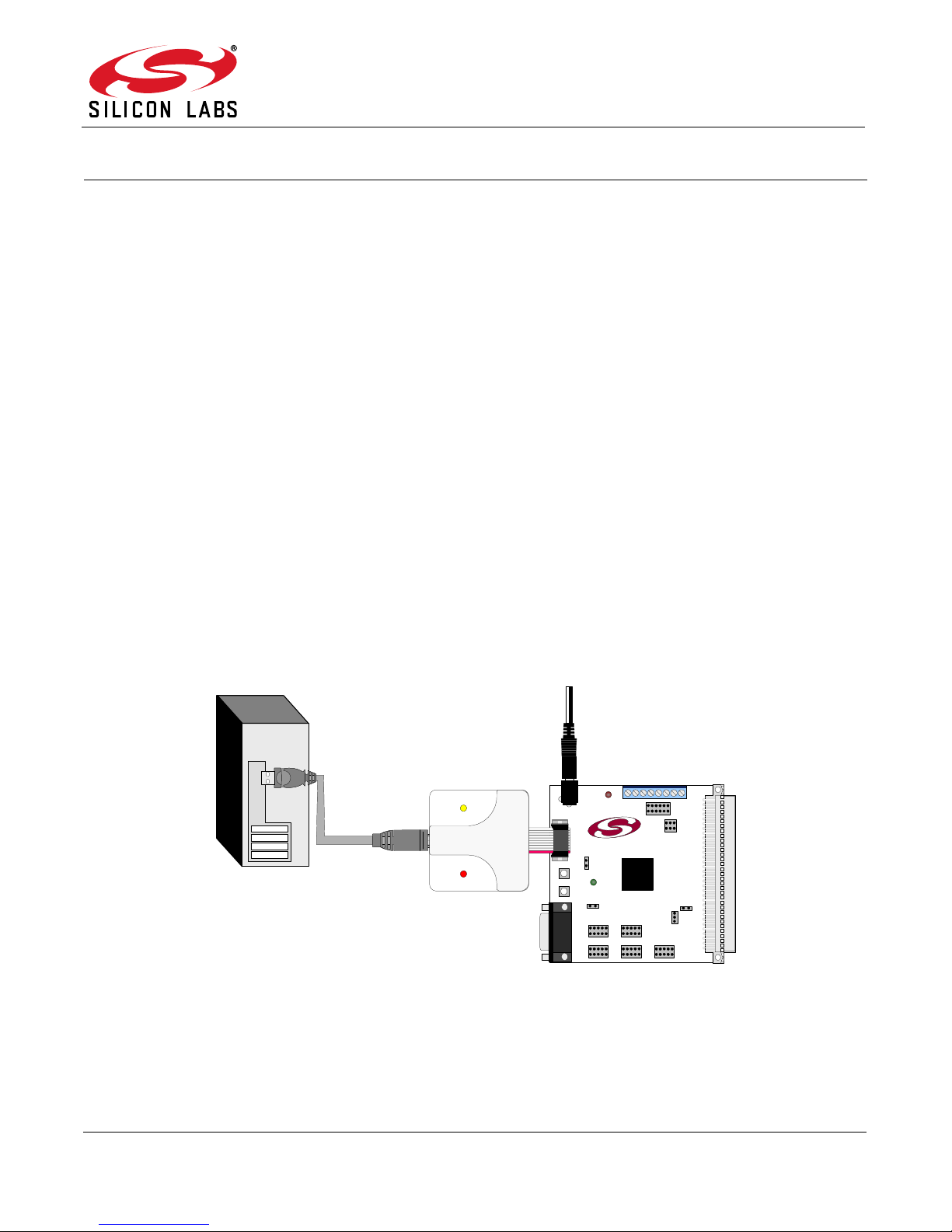
2. Hardware Setup using a USB Debug Adapter
The target board is connected to a PC running the Silicon Laboratories IDE via the USB Debug Adapter as shown
in Figure 1.
1. Connect the USB Debug Adapter to the
DEBUG
connector on the target board with the 10-pin ribbon cable.
2. Connect one end of the USB cable to the USB connector on the USB Debug Adapter.
3. Connect the other end of the USB cable to a USB Port on the PC.
P1
4. Connect the ac/dc power adapter to power jack
on the target board.
Notes:
•Use the Reset button in the IDE to reset the target when connected using a USB Debug Adapter.
• Remove power from the target board and the USB Debug Adapter before connecting or disconnecting the
ribbon cable from the target board. Conn ecting or disconnecting the cable whe n the devices have power can
damage the device and/or the USB Debug Adapter.
Figure 1. Hardware Setup using a USB Debug Adapter
Rev. 0.3 5/14 Copyright © 2014 by Silicon Laboratories C8051F326/7
Page 2
C8051F326/7
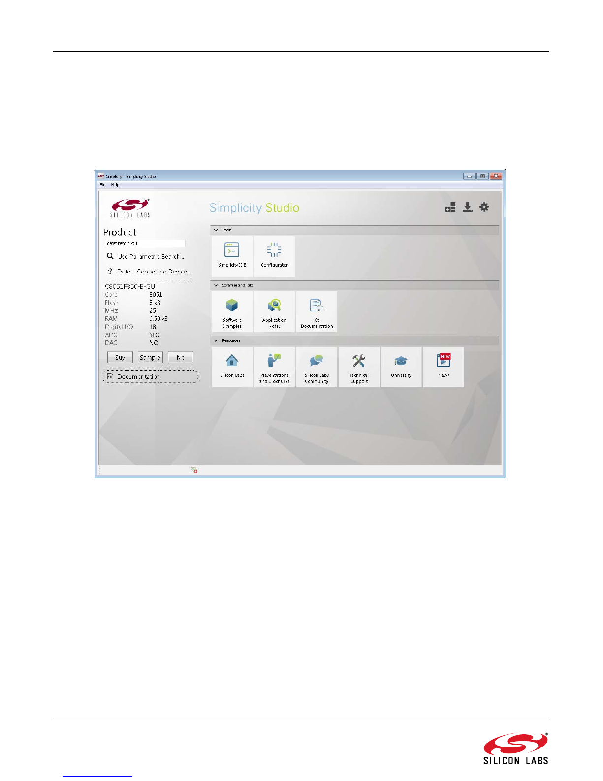
3. Software Setup
Simplicity Studio greatly reduces development time and complexity with Silicon Labs EFM32 and 8051 MCU
products by providing a high-powered IDE, tools for hardware configuration, and links to helpful resources, all in
one place.
Once Simplicity Studio is installed, the application itself can be used to install additional software and
documentation components to aid in the development and evaluation process.
The following Simplicity Studio components are required for the C8051F326 Development Kit:
8051 Products Part Support
Simplicity Developer Platform
Download and install Simplicity Studio from www.silabs.com/8bit-software or www.silabs.com/simplicity-studio.
Once installed, run Simplicity Studio by selecting St art
from the start menu or clicking the Simplicity Studio shortcut on the desktop. Follow the instructions to install the
software and click Simplicity IDE to launch the IDE.
The first time the project creation wizard runs, the Setup Environment wizard will guide the user through the
process of configuring the build tools and SDK selection.
In the Part Selection step of the wizard, select from the list of installed parts only the parts to use during
development. Choosing parts and families in this step affects the displayed or filtered parts in the later device
selection menus. Choose the C8051F326/7 family by checking the C8051F32x check box. Modify the part
selection at any time by accessing the Part Management dialog from the Window
Studio
Simplicity Studio can detect if certain toolchains are not activated. If the Licensing Helper is displayed after
completing the Setup Environment wizard, follow the instructions to activate the toolchain.
2 Rev. 0.3
Part Management menu item.
Figure 2. Simplicity Studio
Silicon LabsSimplicity StudioSimplicity Studio
PreferencesSimplicity
Page 3
C8051F326/7
3.1. Running Blinky
Each project has its own source files, target configuration, SDK configuration, and build configurations such as the
Debug and Release build configurations. The IDE can be used to manage multiple projects in a collection called a
workspace. Workspace settings are applied globally to all projects within the workspace. This can include settings
such as key bindings, window preferences, and code style and formatting options. Project actions, such as build
and debug are context sensitive. For example, the user must select a project in the Project Explorer view in order
to build that project.
To create a project based on the Blinky example:
1. Click the Software Examples tile from the Simplicity Studio home screen.
2. In the Kit drop-down, select C8051F326 Development Kit, in the Part drop-down, select C8051F326, and
in the SDK drop-down, select the desired SDK. Click Next.
3. Select Example and click Next.
4. Under C8051F326 Development Kit in the Blinky folder, select F326-7 BlinkyC and click Next, then
Finish.
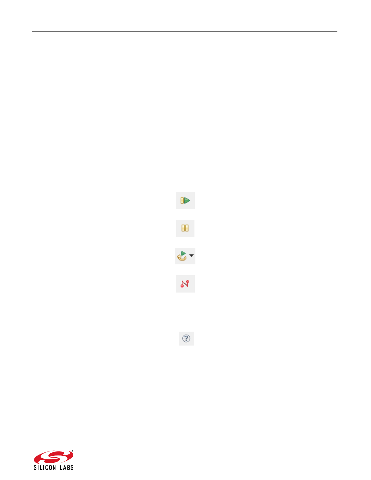
5. Click on the project in the Project Explorer and click Build, the hammer icon in the top bar. Alternatively,
go to Project
6. Click Debug to download the project to the hardware and start a debug session.
7. Press the Resume button to start the code running. The LED should blink.
Build Project.
8. Press the Suspend button to stop the code.
9. Press the Reset the device button to reset the target MCU.
10. Press the Disconnect button to return to the development perspective.
3.2. Simplicity Studio Help
Simplicity Studio includes detailed help information and device documentation within the tool. The help contains
descriptions for each dialog window. To view the documentation for a dialog, click the question mark icon in the
window:
This will open a pane specific to the dialog with additional details.
The documentation within the tool can also be viewed by going to Help
Help Contents or HelpSearch.
Rev. 0.3 3
Page 4
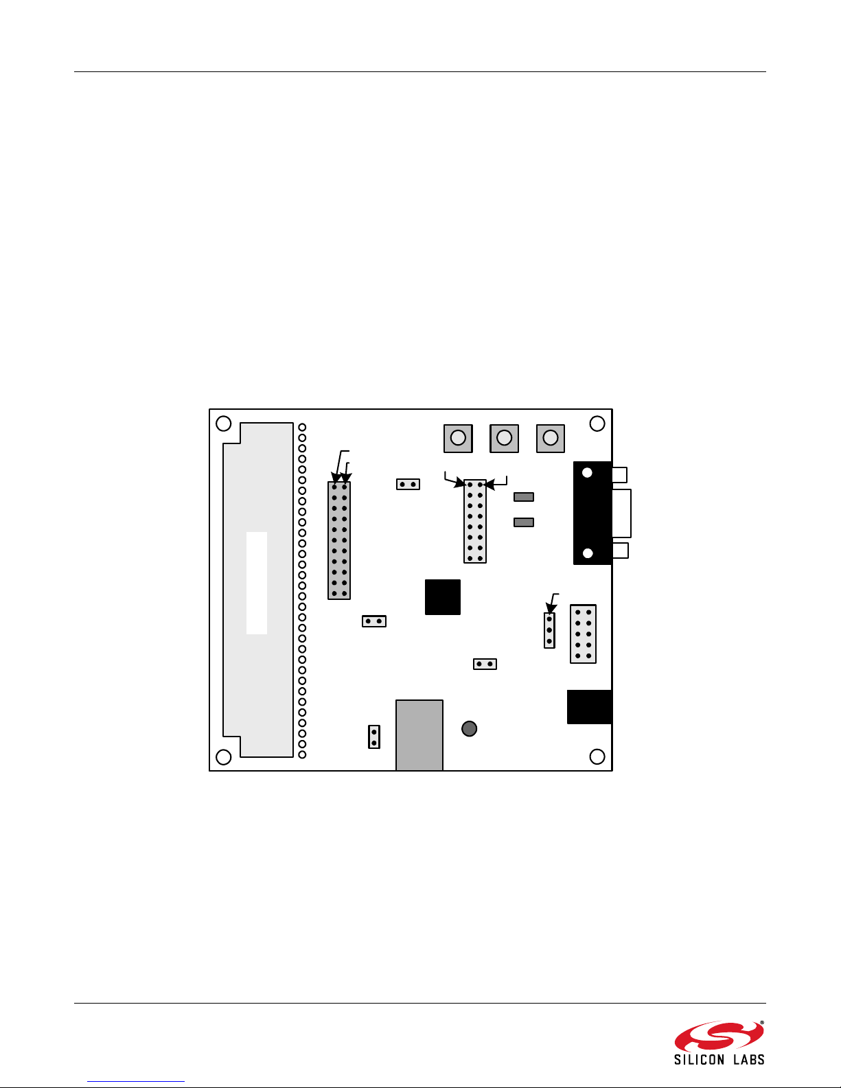
C8051F326/7
DEBUG
P1
J5
Prototype Area
J4
Pin 2
J1
Pin 1
C8051
F326
Pin 1
J8
P2.1 P2.0 RESET
PWR
P2.3
P2.2
J10
J7
J2
Pin 1
Pin 2
J3
J11
J9
4. Target Board
The
C8051F326/7
and preliminary software development. Numerous input/output (I/O) connections are prov ided to facil itate prototy ping using the target board. Refer to
P1Power connector (accepts input from 7 to 15 VDC unregulated power adapter)
J122-pin Expansion I/O connector
J2Power Target Board from power adapter at P1
J3Port I/O Configuration connector
J4DEBUG connector for Debug Adapter interface
J5DB-9 connector for UART0 RS232 interface
J7VIO to VDD connector
J8USB Debug Adapter target board power connector
J9USB connector for USB interface
J10External CMOS oscillator connector
J11Power Target Board from USB at J9
Development Kit includes a target board with a
Figure 3
for the locations of the various I/O connectors.
C8051F326
device pre-installed for evaluation
4 Rev. 0.3
Figure 3. C8051F326 Target Board
Page 5

C8051F326/7
4.1. System Clock Sources
The
C8051F326
enabled as the system clock source on reset. After reset, the internal oscillator operates at a frequency of 1.5 MHz
(±1.5%) by default but may be configured by software to operate at other frequencies. Therefore, in many applications an external oscillator is not required. However , if you wish to opera te the C8051F326 device at a frequency not
available with the internal oscillator, an external CMOS oscillator may be used. Refer to the
for more information on configuring the system clock source.
The target board is designed to facilitate the installation of an external CMOS oscillator. Remove shorting block at
header J10 and connect the oscillator output to the header. Refer to the C8051F326/7 datasheet for more information on the use of external oscillators.
4.2. Switches and LEDs
Three switches are provided on the targe t board. Switch S1 is connected to the /RST pin of the C8051F326. Pressing S1 puts the device into its hardware-reset state. Switches S2 and S3 are connected to the C8051F326’s general purpose I/O (GPIO) pins through headers. Pressing S2 or S3 generates a logic low signal on the port pin.
Remove the shorting blocks from the header to disconnect S2 and S3 from the port pins. The port pin signals are
also routed to pins on the J1 I/O connector. See Table 1 for the port pins and headers corresponding to each
switch.
Three LEDs are also provided on the tar get board . The r ed LED labeled PWR LED is used to indicate a power connection to the target board. The green surface mount LEDs labeled with port pin names are connected to the
C8051F326’s GPIO pins through headers. Remove the shorting blocks from the header to disconnect the LEDs
from the port pin. The port pin signals are also routed to pins on the J1 I/O connector. See Table 1 for the port pins
and headers corresponding to each LED.
device installed on the target board features a calibrated programmable internal oscillator which is
C8051F326/7
datasheet
Table 1. Target Board I/O Descriptions
Description I/O Header
S1 Reset none
S2 P2.0 J3[1–2]
S3 P2.1 J3[3–4]
Green LED (D4) P2.2 J3[5–6]
Green LED (D2) P2.3 J3[7–8]
Red LED PWR none
4.3. Universal Serial Bus (USB) Interface (J9)
A Universal Serial Bus (USB) connector (J9) is provided to facilitate connections to the USB interface on the
C8051F326. Table 2 shows the J9 pin definitions.
Table 2. J9 USB Connector Pin Descriptions
Pin # Description
1 VBUS
2D–
3D+
4 GND (Ground)
Rev. 0.3 5
Page 6

C8051F326/7
4.4. Expansion I/O Connector (J1)
The 22-pin Expansion I/O connector J1 provides access to all signal pins of the C8051F326 device. Pins for +3V,
and digital ground are also available. A through-hole prototyping area is also provided. Each connection point is
labeled indicating the signal availabl e at th e co nn e ction point. See Table 3 for a list of pin descriptions for J1.
Table 3. J1 Pin Descriptions
Pin # Description Pin # Description
1 P0.0 12 P2.3
2 P0.1 13 P2.4
3 P0.2 14 P2.5
4 P0.3 15 P3.0
5P0.4 16C2CK/RST
6P0.5 17VREGIN
7P0.6 18VIO
8 P0.7 19 VBUS
9P2.0 20VDD
10 P2.1 21 +3VD
11 P2.2 22 GND
4.5. USB Self-powered Configuration
The C8051F326 target board can be powered from three different sources. The sources are the ac/dc adapter
(P1), USB connection (J9), and the USB Debug adapter (J4). Only one p owe r so urce sho uld be enab le d at an y
time. See Section 4.8. for infomation on using the USB Debug Adapter as a power source for the board.
The C8051F326 target board can be configured as a self-powered USB device to take power from the USB cable
at J9 instead of the ac/dc adapter connected at P1. To configure the target boards as a self-powered USB device,
remove the shorting block from J2 and install on J11. (A shorting block should only be installed on J2 or J11, never
both at the same time.) Install shorting blocks in the following manner:
J2(ON) & J1 1(OFF)
J2(OFF) & J11(ON)
Notes:
• When the C8051F326 target board is self-p owered fr om th e USB connection ( J9), the EC2 Seri al Adapter is
not powered from the target board. The EC2 Serial Adapter must be powered directly by connecting the ac/
dc adapter to the Serial Adapter’s dc power jack.
• The RS232 Serial Interface (J5) cannot be used when powering the target board from the USB connection (J9).
6 Rev. 0.3
Target Board is powered from the ac/dc Adapter (P1).
Target Board is powered from the USB connection (J9)
Page 7

C8051F326/7
4.6. Target Board DEBUG Interface (J4)
The
DEBUG
Serial Adapter or the USB Debug Adapter to the target board for in-circuit debugging and Flash programming.
Table 4 shows the
4.7. Serial Interface (J5)
A RS232 transceiver circuit and DB-9 (J5) connector are provided on the target board to facilitate serial connections to UART0 of the C8051F326. The TX, RX, RTS and CTS signals of UART0 may be connected to the DB-9
connector and transceiver by installing shorting blocks on head e r J3.
connector (J4) provides access to the
DEBUG
pin definitions.
Table 4. DEBUG Connector Pin Descriptions
Pin # Description
1 +3VD (+3.3VDC)
2, 3, 9 GND (Ground)
4C2D
5/RST (Reset)
6P3.0
7C2CK
8 Not Connected
10 USB Power
DEBUG
(C2) pins of the C8051F326. It is used to connect the
J3[9–10]- Install shorting block to connect UART0 TX (P0.4) to the transceiver.
J3[11–12]- Install shorting block to connect UART0 RX (P0.5) to the transceiver.
J3[13–14]- Install shorting block to connect UART0 RTS (P2.4) to the transceiver.
J3[15–16]- Install shorting block to connect UART0 CTS (P2.5) to the transceiver.
4.8. USB Debug Adapter Target Board Power Connector (J8)
The USB Debug Adapter includes a connection to provide power to the target board. This connection is routed
from J4[10] to J8[1]. Place a shorting block at header J8[2-3] to power the board directly from an ac/dc power
adapter. Place a shorting block at header J8[1–2] to power the board from the USB Debug Adapter. Please note
that the second option is not supported with either the EC1 or EC2 Serial Adapters.
Rev. 0.3 7
Page 8
C8051F326/7
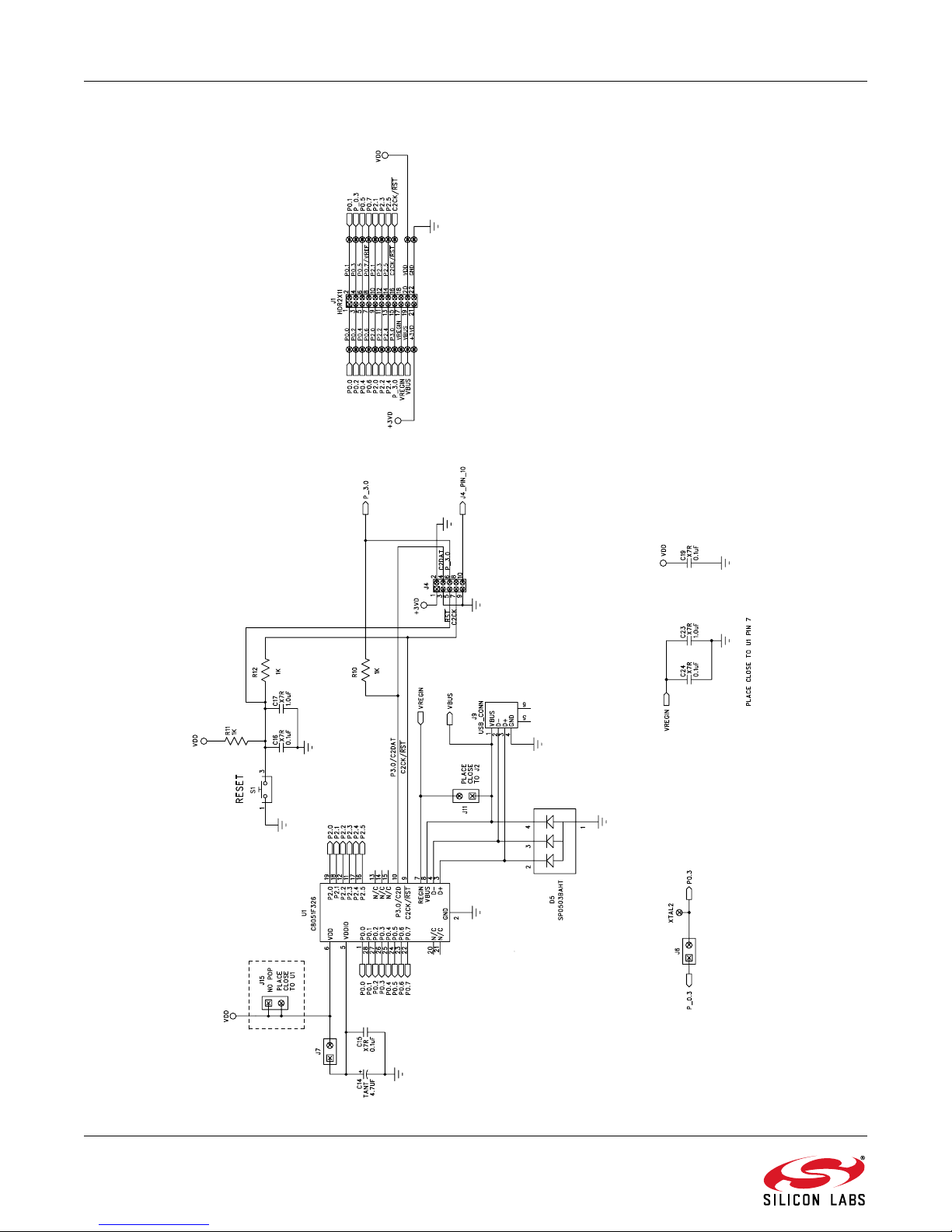
Figure 4. C8051F326 Target Board Schematic (Page 1)
5. Schematics
8 Rev. 0.3
Page 9

C8051F326/7
Figure 5. C8051F326 Target Board Schematic (Page 2)
Rev. 0.3 9
Page 10

C8051F326/7
DOCUMENT CHANGE LIST
Revision 0.1 to Revision 0.2
Removed EC2 Serial Adapter from Kit Contents.
Removed Section 2. Hardware Setup using an EC2 Serial Adapter. See RS232 Serial Adapter (EC2)
User's Guide.
Removed Section 8. EC2 Serial Adapter. See RS232 Serial Adapter (EC2) User's Guide.
Removed Section 9. USB Debug Adapter. See USB Debug Adapter User's Guide.
Revision 0.2 to Revision 0.3
Updated "Software Setup‚" on page 2.
10 Rev. 0.3
Page 11

Simplicity Studio
One-click access to MCU and
wireless tools, documentation,
software, source code libraries &
more. Available for Windows,
Mac and Linux!
IoT Portfolio
www.silabs.com/IoT
Disclaimer
Silicon Laboratories intends to provide customers with the latest, accurate, and in-depth documentation of all peripherals and modules available for system and software implementers
using or intending to use the Silicon Laboratories products. Characterization data, available modules and peripherals, memory sizes and memory addresses refer to each specific
device, and "Typical" parameters provided can and do vary in different applications. Application examples described herein are for illustrative purposes only. Silicon Laboratories
reserves the right to make changes without further notice and limitation to product information, specifications, and descriptions herein, and does not give warranties as to the accuracy
or completeness of the included information. Silicon Laboratories shall have no liability for the consequences of use of the information supplied herein. This document does not imply
or express copyright licenses granted hereunder to design or fabricate any integrated circuits. The products must not be used within any Life Support System without the specific
written consent of Silicon Laboratories. A "Life Support System" is any product or system intended to support or sustain life and/or health, which, if it fails, can be reasonably expected
to result in significant personal injury or death. Silicon Laboratories products are generally not intended for military applications. Silicon Laboratories products shall under no
circumstances be used in weapons of mass destruction including (but not limited to) nuclear, biological or chemical weapons, or missiles capable of delivering such weapons.
Trademark Information
Silicon Laboratories Inc., Silicon Laboratories, Silicon Labs, SiLabs and the Silicon Labs logo, CMEMS®, EFM, EFM32, EFR, Energy Micro, Energy Micro logo and combinations
thereof, "the world’s most energy friendly microcontrollers", Ember®, EZLink®, EZMac®, EZRadio®, EZRadioPRO®, DSPLL®, ISOmodem ®, Precision32®, ProSLIC®, SiPHY®,
USBXpress® and others are trademarks or registered trademarks of Silicon Laboratories Inc. ARM, CORTEX, Cortex-M3 and THUMB are trademarks or registered trademarks of
ARM Holdings. Keil is a registered trademark of ARM Limited. All other products or brand names mentioned herein are trademarks of their respective holders.
Silicon Laboratories Inc.
400 West Cesar Chavez
Austin, TX 78701
USA
SW/HW
www.silabs.com/simplicity
Quality
www.silabs.com/quality
Support and Community
community.silabs.com
http://www.silabs.com
 Loading...