

C8051F320/1
Full Speed USB, 16 k ISP FLASH MCU Family
Analog Peripherals
- 10-Bit ADC
• Up to 200 ksps
• Up to 17 or 13 external single-ended or differential
inputs
• VREF from external pin, internal reference, or VDD
• Built-in temperature sensor
• External conversion start input
- Tw o Comparators
- Internal Voltage Reference
- POR/Brown-Out Detector
USB Function Controller
- USB specification 2.0 compliant
- Full speed (12 Mbps) or low speed (1.5 Mbps)
operation
- Integrated clock recovery; no external crystal
required for full speed or low speed
- Supports eight flexible endpoints
- 1 kB USB buffer memory
- Integrated transceiver; no externa l resi sto rs required
On-Chip Debug
- On-chip debug circuitry facilitates full speed,
non-intrusive in- sy ste m d ebu g (n o em ul ato r req uire d)
- Provides breakpoints, single stepping,
inspect/modify memory and registers
- Superior performance to emulation systems using
ICE-chips, target pods, and sockets
Voltage Regulator Input: 4.0 to 5.25 V
High Speed 8051 µC Core
- Pipelined instruction architecture; executes 70% of
instructions in 1 or 2
system clocks
- Up to 25 MIPS throughput with 25 MHz clock
- Expanded interrupt handler
Memory
- 2304 bytes internal RAM (1k + 256 + 1k USB FIFO)
- 16 kB Flash; In-system programmable in 512-byte
sectors
Digital Peripherals
- 25/21 Port I/O; All 5 V tolerant with high sink current
- Hardware enhanced SPI™, enhanced UART, and
SMBus™ serial ports
- Four gen eral purpose 16-bit c ounter/timers
- 16-bit programmable counter array (PCA) with five
capture/compare modules
- Real time clock mode using external clock source
and PCA or timer
Clock Sources
- Internal Oscillator: 0.25% accuracy with clock
recovery enabled. Supports all USB and UART
modes
- External oscillator: Crystal, RC, C, or Clock
(1 or 2 pin modes)
- Can switch between clock sources on-the-fly;
useful in power saving strategies
RoHS Compliant Packages
- 32-pin LQFP (C8051F320)
- 28-pin QFN (C8051F321)
T e mperature Range: –40 to +85 °C
ANALOG
PERIPHERALS
A
M
U
X
TEMP
SENSOR
10-bit
200 ksps
ADC
PRECISION INTERNAL
OSCILLATOR
+
+
-
VREGVREF
DIGITAL I/O
UART
SPI
SMBus
PCA
Timer 0
Timer 1
Timer 2
Timer 3
USB Controller /
Transceiver
CROSSBAR
Port 0
Port 1
Port 2
Port 3
HIGH-SPEED CONTROLLER CO R E
16 kB
ISP FLASH
16
INTERRUPTS
Rev. 1.2 6/07 Copyright © 2007 by Silicon Laboratories C8051F32x
This information applies to a product under development. Its characteristics and specifications are subject to change without notice.
8051 CPU
(25MIPS)
DEBUG
CIRCUITRY
2304 B
SRAM
POR
WDT

C8051F320/1
2 Rev. 1.2

C8051F320/1
Table of Contents
1. System Overview.................................................................................................... 15
1.1. CIP-51™ Microcontroller Core.......................................................................... 18
1.1.1. Fully 8051 Compatible.............................................................................. 18
1.1.2. Improved Throughput............................................................................... 18
1.1.3. Additional Features. ..... ..... .... ............................ ..... ..... ............................ . 18
1.2. On-Chip Memory............................................................................................... 19
1.3. Universal Serial Bus Controller................................................ ......................... 20
1.4. Voltage Regulator............................................................................................. 21
1.5. On-Chip Debug Circuitry................................................................................... 21
1.6. Programmable Digital I/O and Crossbar........................................................... 22
1.7. Serial Ports....................................................................................................... 23
1.8. Programmable Counter Array........................................................................... 23
1.9. 10-Bit Analog to Digital Converter..................................................................... 24
1.10.Comparators..................................................................................................... 25
2. Absolute Maximum Ratings .................................................................................. 27
3. Global Electrical Characteristics .......................................................................... 28
4. Pinout and Package Definitions............................................................................ 30
5. 10-Bit ADC (ADC0).................................................................................................. 38
5.1. Analog Multiplexer............................................................................................ 39
5.2. Temperature Sensor......................................................................................... 40
5.3. Modes of Operation..........................................................................................42
5.3.1. Starting a Conversion............................................................................... 42
5.3.2. Tracking Modes........................................................................................ 43
5.3.3. Settling Time Requirements..................................................................... 44
5.4. Programmable Window Detector...................................................................... 49
5.4.1. Window Detector In Single-Ended Mode................................................. 51
5.4.2. Window Detector In Differential Mode...................................................... 52
6. Voltage Reference.................................................................................................. 54
7. Comparators ......................................................................................................... 56
8. Voltage Regulator (REG0)...................................................................................... 66
8.1. Regulator Mode Selection................................................................................. 66
8.2. VBUS Detection................................................................................................ 66
9. CIP-51 Microcontroller .......................................................................................... 70
9.1. Instruction Set................................................................................................... 71
9.1.1. Instruction and CPU Timing..................................................................... 71
9.1.2. MOVX Instruction and Program Memory ................................................. 72
9.2. Memory Organization............................................. .... ..... ............................ ..... . 76
9.2.1. Program Memory...................................................................................... 76
9.2.2. Data Memory............................................................................................ 77
9.2.3. General Purpose Registers...................................................................... 77
9.2.4. Bit Addressable Locations........................................................................ 77
9.2.5. Stack ....................................................................................................... 77
9.2.6. Special Function Registers.............. .... ..... ............................ ..... .... ..... ...... 78
Rev. 1.2 3

C8051F320/1
9.2.7. Register Descriptions............................................................................... 82
9.3. Interrupt Handler............................................................................................... 86
9.3.1. MCU Interrupt Sources and Vectors........................................................ 86
9.3.2. External Interrupts.................................................................................... 87
9.3.3. Interrupt Priorities..................................................................................... 87
9.3.4. Interrupt Latency...................................................................................... 88
9.3.5. Interrupt Register Descriptions................................................................. 89
9.4. Power Management Modes.............................................................................. 96
9.4.1. Idle Mode.................................................................................................. 96
9.4.2. Stop Mode................................................................................................ 96
10.Reset Sources ....................................................................................................... 98
10.1.Power-On Reset............................................................................................... 99
10.2.Power-Fail Reset / VDD Monitor .................................................................... 100
10.3.External Reset.................................... ..... .... ..... ............................ ..... .... ..... ....101
10.4.Missing Clock Detector Reset........................................................................ 101
10.5.Comparator0 Reset........................................................................................ 101
10.6.PCA Watchdog Timer Reset ..........................................................................101
10.7.Flash Error Reset........................................................................................... 101
10.8.Software Reset............................................................................................... 102
10.9.USB Reset............................................... .... ..... ..... ............................ .... ..... ....102
11.Flash Memory ..................................................................................................... 105
11.1.Programming The Flash Memory...................................................................105
11.1.1.Flash Lock and Key Functions............................................................... 105
11.1.2.Flash Erase Procedure.......................................................................... 105
11.1.3.Flash Write Procedure........................................................................... 106
11.2.Non-volatile Data Storage......................................... ..... ..... ........................... 106
11.3.Security Options............................................................................................. 107
11.4.Flash Write and Erase Guidelines.................................................................. 109
11.4.1.VDD Maintenance and the VDD Monitor............................................... 109
11.4.2.16.4.2 PSWE Maintenance....................................................................110
11.4.3.System Clock........................ ..... ............................ ..... .... ..... .................. 110
12.External RAM ...................................................................................................... 113
12.1.Accessing User XRAM................................ ..... ..... ............................ .... ..... ....113
12.2.Accessing USB FIFO Space..........................................................................113
13.Oscillators............................................................................................................. 115
13.1.Programmable Internal Oscillator................................................................... 115
13.1.1.Programming the Internal Oscillator on C8051F320/1 Devices............. 116
13.1.2.Internal Oscillator Suspend Mode.......................................................... 117
13.2.External Oscillator Drive Circuit...................................................................... 118
13.2.1.Clocking Timers Directly Through the External Oscillator...................... 118
13.2.2.External Crystal Example....................................................................... 118
13.2.3.External RC Example............................................................................. 119
13.2.4.External Capacitor Example................................................................... 119
13.3.4x Clock Multiplier ........... ..... ..... ............................ .... ..... ..... ........................... 121
13.4.System and USB Clock Selection .................................................................. 122
4 Rev. 1.2

C8051F320/1
13.4.1.System Clock Selection.................................................. ..... .................. 122
13.4.2.USB Clock Selection.............................................................................. 122
14.Port Input/Output ................. ..... ............................ ..... .... ..... ............................ .... 125
14.1.Priority Crossbar Decoder.............................................................................. 127
14.2.Port I/O Initialization....................................................................................... 129
14.3.General Purpose Port I/O.......................................... ..... ............................ ....131
15.Universal Serial Bus Controller (USB)................................................................ 138
15.1.Endpoint Addressing............................................. .... ............................ ..... ....139
15.2.USB Transceiver................................................... .... ............................ ..... ....139
15.3.USB Register Access.............................. .... ............................ ..... ..... .... ..... ....141
15.4.USB Clock Configuration................................................................... .... ..... ....145
15.5.FIFO Management......................................................................................... 146
15.5.1.FIFO Split Mode.....................................................................................146
15.5.2.FIFO Double Buffering........................................................................... 147
15.5.3.FIFO Access.......................................................................................... 147
15.6.Function Addressing.......................................................................................148
15.7.Function Configuration and Control................................................................ 148
15.8.Interrupts........................................................................................................151
15.9.The Serial Interface Engine............................................................................ 156
15.10.Endpoint0..................................................................................................... 156
15.10.1.Endpoint0 SETUP Transactions .......................................................... 157
15.10.2.Endpoint0 IN Transactions................................................................... 157
15.10.3.Endpoint0 OUT Transactions............................................................... 158
15.11.Configuring Endpoints1– 3................ ..... .... ............................ ..... ..... ............. 160
15.12.Controlling Endpoints1–3 IN......................................................................... 161
15.12.1.Endpoints1-3 IN Interrupt or Bulk Mode............................................... 161
15.12.2.Endpoints1-3 IN Isochronous Mode..................................................... 161
15.13.Controlling Endpoints1–3 OUT..................................................................... 164
15.13.1.Endpoints1-3 OUT Interru pt or Bulk Mode.............................. ............. 164
15.13.2.Endpoints1-3 OUT Isochronous Mode................................................. 165
16.SMBus ................................................................................................................... 169
16.1.Supporting Documents................................................................................... 170
16.2.SMBus Configuration......................................................................................170
16.3.SMBus Operation........................................................................................... 170
16.3.1.Arbitration...............................................................................................171
16.3.2.Clock Low Extension.............................................................................. 171
16.3.3.SCL Low Timeout................................................................................... 171
16.3.4.SCL High (SMBus Free) Timeout.......................................................... 172
16.4.Using the SMBus.............................................. ............................ ..... .... ..... ....172
16.4.1.SMBus Configuration Register............................... ..... ........................... 173
16.4.2.SMB0CN Control Register..................................................................... 176
16.4.3.Data Register........................ ............................ ..... ..... .... ....................... 179
16.5.SMBus Transfer Modes.................................................................................. 180
16.5.1.Master Transmitter Mode....................................................................... 180
16.5.2.Master Receiver Mode........................................................................... 181
Rev. 1.2 5

C8051F320/1
16.5.3.Slave Receiver Mode.............................................................................182
16.5.4.Slave Transmitter Mode.........................................................................183
16.6.SMBus Status Decoding.................................................................................184
17.UART0.................................................................................................................... 187
17.1.Enhanced Baud Rate Generation................................................................... 188
17.2.Operational Modes.................... ............................ .... ..... ............................ ....188
17.2.1.8-Bit UART.............................................................................................189
17.2.2.9-Bit UART.............................................................................................190
17.3.Multiprocessor Communications.................................................................... 190
18.Enhanced Serial Peripheral Interface (SPI0)...................................................... 195
18.1.Signal Descriptions.........................................................................................196
18.1.1.Master Out, Slave In (MOSI).................................................................. 196
18.1.2.Master In, Slave Out (MISO).................................................................. 196
18.1.3.Serial Clock (SCK)................................................................................. 196
18.1.4.Slave Select (NSS)................................................................................ 196
18.2.SPI0 Master Mode Operation ......................................................................... 197
18.3.SPI0 Slave Mode Operation........................................................................... 198
18.4.SPI0 Interrupt Sources................................................................................... 199
18.5.Serial Clock Timing........................ ..... ..... .... ..... ............................ ..... .... ..... ....199
18.6.SPI Special Function Registers...................................................................... 202
19. Timers ................................................................................................................... 209
19.1.Timer 0 and Timer 1....................................................................................... 209
19.1.1.Mode 0: 13-bit Counter/Timer................................................................ 209
19.1.2.Mode 1: 16-bit Counter/Timer................................................................ 211
19.1.3.Mode 2: 8-bit Counter/Timer with Auto-Reload...................................... 211
19.1.4.Mode 3: Two 8-bit Counter/Timers (Timer 0 Only)................................. 212
19.2.Timer 2 ..........................................................................................................217
19.2.1.16-bit Timer with Auto-Reload................................................................ 217
19.2.2.8-bit Timers with Auto-Reload................................................................218
19.2.3.USB Start-of-Frame Capture.................................................................. 219
19.3.Timer 3 ..........................................................................................................222
19.3.1.16-bit Timer with Auto-Reload................................................................ 222
19.3.2.8-bit Timers with Auto-Reload................................................................223
19.3.3.USB Start-of-Frame Capture.................................................................. 224
20.Programmable Counter Array (PCA0) ............. ..... ............................ ..... .... ..... .... 227
20.1.PCA Counter/Timer................................. .... ............................ ..... ..... .... ......... 228
20.2.Capture/Compare Modules............................................................................ 229
20.2.1.Edge-triggered Capture Mode................................................................ 230
20.2.2.Software Timer (Compare) Mode........................................................... 232
20.2.3.High Speed Output Mode....................................................................... 233
20.2.4.Frequency Output Mode........................................ ..... .... ..... .................. 234
20.2.5.8-Bit Pulse Width Modulator Mode......................................................... 235
20.2.6.16-Bit Pulse Width Modulator Mode.......................................................236
20.3.Watchdog Timer Mode................................................................................... 236
20.3.1.Watchdog Timer Operation....................................................................237
6 Rev. 1.2

C8051F320/1
20.3.2.Watchdog Timer Usage......................................................................... 238
20.4.Register Descriptions for PCA........................................................................ 239
21.C2 Interface................................. ..... .... ..... ............................ ..... .... ....................... 245
21.1.C2 Interface Registers.................................................................................... 245
21.2.C2 Pin Sharing............................................................................................... 247
Rev. 1.2 7

C8051F320/1
List of Figures and Tables
1. System Overview
Table 1.1. Product Selection Guide........................................................................ 16
Figure 1.1. C8051F320 Block Diagram.................................................................... 16
Figure 1.2. C8051F321 Block Diagram.................................................................... 17
Figure 1.3. On-Chip Clock and Reset ...................................................................... 19
Figure 1.4. On-Board Memory Map.......................................................................... 20
Figure 1.5. USB Controller Block Diagram............................................................... 21
Figure 1.6. Development/In-System Debug Diagram............................................... 22
Figure 1.7. Digital Crossbar Diagram....................................................................... 23
Figure 1.8. PCA Block Diagram ............................................................................... 24
Figure 1.9. PCA Block Diagram ............................................................................... 24
Figure 1.10. 10-Bit ADC Block Diagram................................................................... 25
Figure 1.11. Comparator0 Block Diagram................................................................ 26
2. Absolute Maximum Ratings
Table 2.1. Absolute Maximum Ratings .................................................................... 27
3. Global Electrical Characteristics
Table 3.1. Global Electrical Characteristics ............................................................. 28
Table 3.2. Index to Electrical Characteristics Tables.............................................. 29
4. Pinout and Package Definitions
Table 4.1. Pin Definitions for the C8051F320/1...................................................... 30
Figure 4.1. LQFP-32 Pinout Diagram (Top View) .................................................... 32
Figure 4.2. LQFP-32 Package Diagram................................................................... 33
Table 4.2. LQFP-32 Package Dimensions.............................................................. 33
Figure 4.3. QFN-28 Pinout Diagram (Top View)...................................................... 34
Figure 4.4. QFN-28 Package Drawing..................................................................... 35
Table 4.3. QFN-28 Package Dimensions................................................................ 35
Figure 4.5. Typical QFN-28 Landing Diagram.......................................................... 36
Figure 4.6. QFN-28 Solder Paste Recommendation................................................37
5. 10-Bit ADC (ADC0)
Figure 5.1. ADC0 Functional Block Diagram............................................................ 38
Figure 5.2. Temperature Sensor Transfer Function................................................. 40
Figure 5.3. Temperature Sensor Error with 1-Point Calibration (VREF = 2.40 V).... 41
Figure 5.4. 10-Bit ADC Track and Conversion Example Timing.............................. 43
Figure 5.5. ADC0 Equivalent Input Circuits.............................................................. 44
Figure 5.6. ADC Window Compare Example: Right-Justified Single-Ended Data... 51
Figure 5.7. ADC Window Compare Example: Left-Justified Single-Ended Data ..... 51
Figure 5.8. ADC Window Compare Example: Right-Justified Differential Data ....... 52
Figure 5.9. ADC Window Compare Example: Left-Justified Differential Data.......... 52
Table 5.1. ADC0 Electrical Characteristics ............................................................. 53
6. Voltage Reference
Figure 6.1. Voltage Reference Functional Block Diagram....................................... 54
Table 6.1. Voltage Reference Electrical Characteristics ......................................... 55
8 Rev. 1.2

C8051F320/1
7. Comparators
Figure 7.1. Comparator0 Functional Block Diagram................................................ 56
Figure 7.2. Comparator1 Functional Block Diagram................................................ 57
Figure 7.3. Comparator Hysteresis Plot................................................................... 58
Table 7.1. Comparator Electrical Characteristics .................................................... 65
8. Voltage Regulator (REG0)
Figure 8.1. External Capacitors for Voltage Regulator Input/Output........................ 66
Table 8.1. Voltage Regulator Electrical Specifications ............................................ 67
Figure 8.2. REG0 Configuration: USB Bus-Powered............................................... 67
Figure 8.3. REG0 Configuration: USB Self-Powered............................................... 68
Figure 8.4. REG0 Configuration: USB Self-Powered, Regulator Disabled .............. 68
Figure 8.5. REG0 Configuration: No USB Connection............................................. 69
9. CIP-51 Microc ontroller
Figure 9.1. CIP-51 Block Diagram............................................................................ 70
Table 9.1. CIP-51 Instruction Set Summary............................................................ 72
Figure 9.2. Memory Map.......................................................................................... 76
Table 9.2. Special Function Register (SFR) Memory Map...................................... 78
Table 9.3. Special Function Registers ............... ..... ..... .... ............................ ..... ..... . 79
Table 9.4. Interrupt Summary ................................................................................. 88
10.Reset Sources
Figure 10.1. Reset Sources...................................................................................... 98
Figure 10.2. Power-On and VDD Monitor Reset Timing .......................................... 99
Table 10.1. Reset Electrical Characteristics .......................................................... 104
11.Flash Memory
Table 11.1. Flash Electrical Characteristics .......................................................... 106
Figure 11.1. Flash Program Memory Map and Secu rity Byte............................. ....107
Table 11.2. Flash Security Summary..................................................................... 108
12.External RAM
Figure 12.1. External Ram Memory Map................................................................113
Figure 12.2. XRAM Memory Map Expanded View................................................. 114
13.Oscillators
Figure 13.1. Oscillator Diagram.............................................................................. 115
Table 13.1. Typical USB Full Speed Clock Settings...............................................122
Table 13.2. Typical USB Low Speed Clock Settings..............................................123
Table 13.3. Internal Oscillator Electrical Characteristics ....................................... 124
14.Port Input/Output
Figure 14.1. Port I/O Functional Block Diagram..................................................... 125
Figure 14.2. Port I/O Cell Block Diagram............................................................... 126
Figure 14.3. Crossbar Priority Decoder with No Pins Skipped............................... 127
Figure 14.4. Crossbar Priority Decoder with Crystal Pins Skipped ........................ 128
Table 14.1. Port I/O DC Electrical Characteristics ................................................ 137
15.Universal Serial Bus Controller (USB)
Figure 15.1. USB0 Block Diagram.......................................................................... 138
Table 15.1. Endpoint Addressing Scheme............................................................. 139
Figure 15.2. USB0 Register Access Scheme ......................................................... 141
Rev. 1.2 9

C8051F320/1
Table 15.2. USB0 Controller Registers ..................................................................143
Figure 15.3. USB FIFO Allocation..........................................................................146
Table 15.3. FIFO Configurations............................................................................ 147
Table 15.4. USB Transceiver Electrical Characteristics ........................................ 168
16.SMBus
Figure 16.1. SMBus Block Diagram....................................................................... 169
Figure 16.2. Typical SMBus Configuration............................................................. 170
Figure 16.3. SMBus Transaction............................................................................ 171
Table 16.1. SMBus Clock Source Selection ........................................................... 173
Figure 16.4. Typical SMBus SCL Generation.........................................................174
Table 16.2. Minimum SDA Setup and Hold Times................................................. 174
Table 16.3. Sources for Hardware Changes to SMB0CN...................................... 178
Figure 16.5. Typical Master Transmitter Sequence................................................ 180
Figure 16.6. Typical Master Receiver Sequence.................................................... 181
Figure 16.7. Typical Slave Receiver Sequence...................................................... 182
Figure 16.8. Typical Slave Transmitter Sequence..................................................183
Table 16.4. SMBus Status Decoding...................................................................... 184
17.UART0
Figure 17.1. UART0 Block Diagram....................................................................... 187
Figure 17.2. UART0 Baud Rate Logic............................................. ..... ..... .... ..... ....188
Figure 17.3. UART Interconnect Diagram.............................................................. 189
Figure 17.4. 8-Bit UART Timing Diagram............................................................... 189
Figure 17.5. 9-Bit UART Timing Diagram............................................................... 190
Figure 17.6. UART Multi-Processor Mode Interconnect Diagram.......................... 191
Table 17.1. Timer Settings for Standard Baud Rates Using The Internal Oscillator 194
18.Enhanced Serial Peri pheral Interfac e (SPI0)
Figure 18.1. SPI Block Diagram............................................................................. 195
Figure 18.2. Multiple-Master Mode Connection Diagram....................................... 198
Figure 18.3. 3-Wire Single Master and Slave Mode Connection Diagram............. 198
Figure 18.4. 4-Wire Single Master Mode and 4-Wire
Slave Mode Connection Diagram.............................................. ..... ....198
Figure 18.5. Master Mode Data/Clock Timing........................................................ 200
Figure 18.6. Slave Mode Data/Clock Timing (CKPHA = 0).................................... 200
Figure 18.7. Slave Mode Data/Clock Timing (CKPHA = 1).................................... 201
Figure 18.8. SPI Master Timing (CKPHA = 0)........................................................ 206
Figure 18.9. SPI Master Timing (CKPHA = 1)........................................................ 206
Figure 18.10. SPI Slave Timing (CKPHA = 0)........................................................207
Figure 18.11. SPI Slave Timing (CKPHA = 1)........................................................207
Table 18.1. SPI Slave Timing Parameters ............................................................. 208
19.Timers
Figure 19.1. T0 Mode 0 Block Diagram.................................................................. 210
Figure 19.2. T0 Mode 2 Block Diagram.................................................................. 211
Figure 19.3. T0 Mode 3 Block Diagram.................................................................. 212
Figure 19.4. Timer 2 16-Bit Mode Block Diagram .................................................. 217
Figure 19.5. Timer 2 8-Bit Mode Block Diagram .................................................... 218
10 Rev. 1.2

C8051F320/1
Figure 19.6. Timer 2 SOF Capture Mode (T2SPLIT = ‘0’)...................................... 219
Figure 19.7. Timer 2 SOF Capture Mode (T2SPLIT = ‘1’)...................................... 219
Figure 19.8. Timer 3 16-Bit Mode Block Diagram .................................................. 222
Figure 19.9. Timer 3 8-Bit Mode Block Diagram .................................................... 223
Figure 19.10. Timer 3 SOF Capture Mode (T3SPLIT = ‘0’).................................... 224
Figure 19.11. Timer 3 SOF Capture Mode (T3SPLIT = ‘1’).................................... 224
20.Programmable Counter Array (PCA0)
Figure 20.1. PCA Block Diagram............................................................................ 227
Table 20.1. PCA Timebase Input Options.............................................................. 228
Figure 20.2. PCA Counter/Timer Block Diagram....................................................228
Table 20.2. PCA0CPM Register Settings for PCA Capture/Compare Modules..... 229
Figure 20.3. PCA Interrupt Block Diagram............................................................. 230
Figure 20.4. PCA Capture Mode Diagram.............................................................. 231
Figure 20.5. PCA Software Timer Mode Diagram.................................................. 232
Figure 20.6. PCA High Speed Output Mode Diagram............................................233
Figure 20.7. PCA Frequency Output Mode............................................................234
Figure 20.8. PCA 8-Bit PWM Mode Diagram......................................................... 235
Figure 20.9. PCA 16-Bit PWM Mode...................................................................... 236
Figure 20.10. PCA Module 4 with Watchdog Timer Enabled................................. 237
Table 20.3. Watchdog Timer Timeout Intervals...................................................... 239
21.C2 Interface
Figure 21.1. Typical C2 Pin Sharing....................................................................... 247
Rev. 1.2 11

C8051F320/1
List of Registers
SFR Definition 5.1. AMX0P: AMUX0 Positive Channel Select . . . . . . . . . . . . . . . . . . 45
SFR Definition 5.2. AM X0 N: AMU X0 Ne ga ti ve Ch an nel Select . . . . . . . . . . . . . . . . . . 46
SFR Definition 5.3. ADC0CF: ADC0 Configuration . . . . . . . . . . . . . . . . . . . . . . . . . . . 47
SFR Definition 5.4. ADC0H: ADC0 Data Word MSB . . . . . . . . . . . . . . . . . . . . . . . . . . 47
SFR Definition 5.5. ADC0L: ADC0 Data Word LSB . . . . . . . . . . . . . . . . . . . . . . . . . . . 47
SFR Definition 5.6. ADC0CN: ADC0 Control . . . . . . . . . . . . . . . . . . . . . . . . . . . . . . . . 48
SFR Definition 5.7. ADC0GTH: ADC0 Greater-Than Data High Byte . . . . . . . . . . . . . 49
SFR Definition 5.8. ADC0GTL: ADC0 Greater-Than Data Low Byte . . . . . . . . . . . . . 49
SFR Definition 5.9. ADC0LTH: ADC0 Less-Than Data High Byte . . . . . . . . . . . . . . . . 50
SFR Definition 5.10. ADC0LTL: ADC0 Less-Than Data Low Byte . . . . . . . . . . . . . . . 50
SFR Definition 6.1. REF0CN: Reference Control . . . . . . . . . . . . . . . . . . . . . . . . . . . . . 55
SFR Definition 7.1. CPT0CN: Comparator0 Control . . . . . . . . . . . . . . . . . . . . . . . . . . . 59
SFR Definition 7.2. CPT0MX: Comparator0 MUX Selection . . . . . . . . . . . . . . . . . . . . 60
SFR Definition 7.3. CPT0MD: Comparator0 Mode Selection . . . . . . . . . . . . . . . . . . . . 61
SFR Definition 7.4. CPT1CN: Comparator1 Control . . . . . . . . . . . . . . . . . . . . . . . . . . . 62
SFR Definition 7.5. CPT1MX: Comparator1 MUX Selection . . . . . . . . . . . . . . . . . . . . 63
SFR Definition 7.6. CPT1MD: Comparator1 Mode Selection . . . . . . . . . . . . . . . . . . . . 64
SFR Definition 8.1. REG0CN: Voltage Regulator Control . . . . . . . . . . . . . . . . . . . . . . 69
SFR Definition 9.1. DPL: Data Pointer Low Byte . . . . . . . . . . . . . . . . . . . . . . . . . . . . . 82
SFR Definition 9.2. DPH: Data Pointer High Byte . . . . . . . . . . . . . . . . . . . . . . . . . . . . . 83
SFR Definition 9.3. SP: Stack Pointer . . . . . . . . . . . . . . . . . . . . . . . . . . . . . . . . . . . . . . 83
SFR Definition 9.4. PSW: Program Status Word . . . . . . . . . . . . . . . . . . . . . . . . . . . . . 84
SFR Definition 9.5. ACC: Accumulator . . . . . . . . . . . . . . . . . . . . . . . . . . . . . . . . . . . . . 85
SFR Definition 9.6. B: B Register . . . . . . . . . . . . . . . . . . . . . . . . . . . . . . . . . . . . . . . . . 85
SFR Definition 9.7. IE: Interrupt Enable . . . . . . . . . . . . . . . . . . . . . . . . . . . . . . . . . . . . 90
SFR Definition 9.8. IP: Interrupt Priority . . . . . . . . . . . . . . . . . . . . . . . . . . . . . . . . . . . . 91
SFR Definition 9.9. EIE1: Extended Interrupt Enable 1 . . . . . . . . . . . . . . . . . . . . . . . . 92
SFR Definition 9.10. EIP1: Extended Interrupt Priority 1 . . . . . . . . . . . . . . . . . . . . . . . 93
SFR Definition 9.11. EIE2: Extended Interrupt Enable 2 . . . . . . . . . . . . . . . . . . . . . . . 94
SFR Definition 9.12. EIP2: Extended Interrupt Priority 2 . . . . . . . . . . . . . . . . . . . . . . . 94
SFR Definition 9.13. IT01CF: INT0/INT1 Configuration . . . . . . . . . . . . . . . . . . . . . . . . 95
SFR Definition 9.14. PCON: Power Control . . . . . . . . . . . . . . . . . . . . . . . . . . . . . . . . . 97
SFR Definition 10.1. VDM0CN: VDD Monitor Control . . . . . . . . . . . . . . . . . . . . . . . . 100
SFR Definition 10.2. RSTSRC: Reset Source . . . . . . . . . . . . . . . . . . . . . . . . . . . . . . 103
SFR Definition 11.1. PSCTL: Program Store R/W Control . . . . . . . . . . . . . . . . . . . . . 111
SFR Definition 11.2. FLKEY: Flash Lock and Key . . . . . . . . . . . . . . . . . . . . . . . . . . . 111
SFR Definition 11.3. FLSCL: Flash Scale . . . . . . . . . . . . . . . . . . . . . . . . . . . . . . . . . . 112
SFR Definition 12.1. EMI0CN: External Memory Interface Control . . . . . . . . . . . . . . 114
SFR Definition 13.1. OSCICN: Internal Oscillator Control . . . . . . . . . . . . . . . . . . . . .117
SFR Definition 13.2. OSCICL: Internal Oscillator Calibration . . . . . . . . . . . . . . . . . . .117
SFR Definition 13.3. OSCXCN: External Oscillator Control . . . . . . . . . . . . . . . . . . . . 120
SFR Definition 13.4. CLKMUL: Clock Multiplier Control . . . . . . . . . . . . . . . . . . . . . . . 121
SFR Definition 13.5. CLKSEL: Clock Select . . . . . . . . . . . . . . . . . . . . . . . . . . . . . . . . 123
12 Rev. 1.2

C8051F320/1
SFR Definition 14.1. XBR0: Port I/O Crossbar Register 0 . . . . . . . . . . . . . . . . . . . . . 130
SFR Definition 14.2. XBR1: Port I/O Crossbar Register 1 . . . . . . . . . . . . . . . . . . . . . 131
SFR Definition 14.3. P0: Port0 Register . . . . . . . . . . . . . . . . . . . . . . . . . . . . . . . . . . .132
SFR Definition 14.4. P0MDIN: Port0 Input Mode Register . . . . . . . . . . . . . . . . . . . . . 132
SFR Definition 14.5. P0MDOUT: Port0 Output Mode Register . . . . . . . . . . . . . . . . . 132
SFR Definition 14.6. P0SKIP: Port0 Skip Register . . . . . . . . . . . . . . . . . . . . . . . . . . . 133
SFR Definition 14.7. P1: Port1 Register . . . . . . . . . . . . . . . . . . . . . . . . . . . . . . . . . . .133
SFR Definition 14.8. P1MDIN: Port1 Input Mode Register . . . . . . . . . . . . . . . . . . . . . 133
SFR Definition 14.9. P1MDOUT: Port1 Output Mode Register . . . . . . . . . . . . . . . . . 134
SFR Definition 14.10. P1SKIP: Port1 Skip Register . . . . . . . . . . . . . . . . . . . . . . . . . .134
SFR Definition 14.11. P2: Port2 Register . . . . . . . . . . . . . . . . . . . . . . . . . . . . . . . . . .134
SFR Definition 14.12. P2MDIN: Port2 Input Mode Register . . . . . . . . . . . . . . . . . . . . 135
SFR Definition 14.13. P2MDOUT: Port2 Output Mode Register . . . . . . . . . . . . . . . .135
SFR Definition 14.14. P2SKIP: Port2 Skip Register . . . . . . . . . . . . . . . . . . . . . . . . . .135
SFR Definition 14.15. P3: Port3 Register . . . . . . . . . . . . . . . . . . . . . . . . . . . . . . . . . .136
SFR Definition 14.16. P3MDIN: Port3 Input Mode Register . . . . . . . . . . . . . . . . . . . . 136
SFR Definition 14.17. P3MDOUT: Port3 Output Mode Register . . . . . . . . . . . . . . . .136
SFR Definition 15.1. USB0XCN: USB0 Transceiver Control . . . . . . . . . . . . . . . . . . . 140
SFR Definition 15.2. USB0ADR: USB0 Indirect Address . . . . . . . . . . . . . . . . . . . . . . 142
SFR Definition 15.3. USB0DAT: USB0 Data . . . . . . . . . . . . . . . . . . . . . . . . . . . . . . . 143
USB Register Definition 15.4. INDEX: USB0 Endpoint Index . . . . . . . . . . . . . . . . . . . 144
USB Register Definition 15.5. CLKREC: Clock Recovery Control . . . . . . . . . . . . . . . 145
USB Register Definition 15.6. FIFOn: USB0 Endpoint FIFO Access . . . . . . . . . . . . . 147
USB Register Definition 15.7. FADDR: USB0 Function Address . . . . . . . . . . . . . . . . 148
USB Register Definition 15.8. POWER: USB0 Power . . . . . . . . . . . . . . . . . . . . . . . . 150
USB Register Definition 15.9. FRAMEL: USB0 Frame Number Low . . . . . . . . . . . . . 151
USB Register Definition 15.10. FRAMEH: USB0 Frame Number High . . . . . . . . . . . 151
USB Register Definition 15.11. IN1INT: USB0 IN Endpoint Interrupt . . . . . . . . . . . . 152
USB Register Definition 15.12. OUT1INT: USB0 Out Endpoint Interrupt . . . . . . . . . . 153
USB Register Definition 15.13. CMINT: USB0 Common Interrupt . . . . . . . . . . . . . . .154
USB Register Definition 15.14. IN1IE: USB0 IN Endpoint Interrupt Enable . . . . . . . . 155
USB Register Definition 15.15. OUT1IE: USB0 Out Endpoint Interrupt Enable . . . . . 155
USB Register Definition 15.16. CMIE: USB0 Common Interrupt Enable . . . . . . . . . . 156
USB Register Definition 15.17. E0CSR: USB0 Endpoint0 Control . . . . . . . . . . . . . . . 159
USB Register Definition 15.18. E0CNT: USB0 Endpoint 0 Data Count . . . . . . . . . . . 160
USB Register Definition 15.19. INMAX: USB0 IN Endpoint n Maximum Packet Size 160
USB Register Definition 15.20. EINCSRL: USB0 IN Endpoint Con trol Low Byte . . . . 163
USB Register Definition 15.21. EINCSRH: USB0 IN Endpoint Control High Byte . . . 164
USB Register Definition 15.22. OUTMAX: USB0 Out Endpoint Max Packet Size . . . 165
USB Register Definition 15.23. EOUTCSRL: USB0 OUT Endpoint Control High Byte 166
USB Register Definition 15.24. EOUTCSRH: USB0 OUT Endpoint Control Low Byte 167
USB Register Definition 15.25. EOUTCNTL: USB0 OUT Endpoint Count Low . . . . .167
USB Register Definition 15.26. EOUTCNTH: USB0 OUT Endpoint Count High . . . . 167
SFR Definition 16.1. SMB0CF: SMBus Clock/Configuration . . . . . . . . . . . . . . . . . . . 175
SFR Definition 16.2. SMB0CN: SMBus Control . . . . . . . . . . . . . . . . . . . . . . . . . . . . . 177
Rev. 1.2 13

C8051F320/1
SFR Definition 16.3. SMB0DAT: SMBus Data . . . . . . . . . . . . . . . . . . . . . . . . . . . . . .179
SFR Definition 17.1. SCON0: Serial Port 0 Control . . . . . . . . . . . . . . . . . . . . . . . . . . 192
SFR Definition 17.2. SBUF0: Serial (UART0) Port Data Buffer . . . . . . . . . . . . . . . . . 193
SFR Definition 18.1. SPI0CFG: SPI0 Configuration . . . . . . . . . . . . . . . . . . . . . . . . . . 203
SFR Definition 18.2. SPI0CN: SPI0 Control . . . . . . . . . . . . . . . . . . . . . . . . . . . . . . . . 204
SFR Definition 18.3. SPI0CKR: SPI0 Clock Rate . . . . . . . . . . . . . . . . . . . . . . . . . . . . 205
SFR Definition 18.4. SPI0DAT: SPI0 Data Register . . . . . . . . . . . . . . . . . . . . . . . . . . 205
SFR Definition 19.1. TCON: Timer Control . . . . . . . . . . . . . . . . . . . . . . . . . . . . . . . . . 213
SFR Definition 19.2. TMOD: Timer Mode . . . . . . . . . . . . . . . . . . . . . . . . . . . . . . . . . .214
SFR Definition 19.3. CKCON: Clock Control . . . . . . . . . . . . . . . . . . . . . . . . . . . . . . . 215
SFR Definition 19.4. TL0: Timer 0 Low Byte . . . . . . . . . . . . . . . . . . . . . . . . . . . . . . . . 216
SFR Definition 19.5. TL1: Timer 1 Low Byte . . . . . . . . . . . . . . . . . . . . . . . . . . . . . . . . 216
SFR Definition 19.6. TH0: Timer 0 High Byte . . . . . . . . . . . . . . . . . . . . . . . . . . . . . . . 216
SFR Definition 19.7. TH1: Timer 1 High Byte . . . . . . . . . . . . . . . . . . . . . . . . . . . . . . . 216
SFR Definition 19.8. TMR2CN: Timer 2 Control . . . . . . . . . . . . . . . . . . . . . . . . . . . . . 220
SFR Definition 19.9. TMR2RLL: Timer 2 Reload Register Low Byte . . . . . . . . . . . . . 221
SFR Definition 19.10. TMR2 RLH: Timer 2 Reload Register High Byte . . . . . . . . . . . 221
SFR Definition 19.11. TMR2L: Timer 2 Low Byte . . . . . . . . . . . . . . . . . . . . . . . . . . . . 221
SFR Definition 19.12. TMR2H Timer 2 High Byte . . . . . . . . . . . . . . . . . . . . . . . . . . . . 221
SFR Definition 19.13. TMR3CN: Timer 3 Control . . . . . . . . . . . . . . . . . . . . . . . . . . . . 225
SFR Definition 19.14. TMR3RLL: Timer 3 Reload Register Low Byte . . . . . . . . . . . . 226
SFR Definition 19.15. TMR3 RLH: Timer 3 Reload Register High Byte . . . . . . . . . . . 226
SFR Definition 19.16. TMR3L: Timer 3 Low Byte . . . . . . . . . . . . . . . . . . . . . . . . . . . . 226
SFR Definition 19.17. TMR3H Timer 3 High Byte . . . . . . . . . . . . . . . . . . . . . . . . . . . . 226
SFR Definition 20.1. PCA0CN: PCA Control . . . . . . . . . . . . . . . . . . . . . . . . . . . . . . . 240
SFR Definition 20.2. PCA0MD: PCA Mode . . . . . . . . . . . . . . . . . . . . . . . . . . . . . . . . 241
SFR Definition 20.3. PCA0CPMn: PCA Capture/Compare Mode . . . . . . . . . . . . . . . 242
SFR Definition 20.4. PCA0L: PCA Counter/Timer Low Byte . . . . . . . . . . . . . . . . . . . 243
SFR Definition 20.5. PCA0H: PCA Counter/Timer High Byte . . . . . . . . . . . . . . . . . . 243
SFR Definition 20.6. PCA0CPLn: PCA Capture Module Low Byte . . . . . . . . . . . . . . . 243
SFR Definition 20.7. PCA0CPHn: PCA Capture Module High Byte . . . . . . . . . . . . . . 244
C2 Register Definition 21.1. C2ADD: C2 Address . . . . . . . . . . . . . . . . . . . . . . . . . . . 245
C2 Register Definition 21.2. C2 Device ID . . . . . . . . . . . . . . . . . . . . . . . . . . . . . . . . . 245
C2 Register Definition 21.3. REVID: C2 Revision ID . . . . . . . . . . . . . . . . . . . . . . . . . 246
C2 Register Definition 21.4. FPCTL: C2 Flash Programming Control . . . . . . . . . . . . 246
C2 Register Definition 21.5. FPDAT: C2 Flash Programming Data . . . . . . . . . . . . . . 246
14 Rev. 1.2

C8051F320/1
1. System Overview
C8051F320/1 devices a r e fu ll y int egrate d m ix ed-s ig nal S ystem - on-a- Chip MCUs. Highlighted fe atu res ar e
listed below. Refer to
• High-speed pipelined 8051-compatible microcontroller core (up to 25 MIPS)
• In-system, full-speed, non-intrusive debug interface (on-chip)
• Universal Serial Bus (USB) Function Controller with eight flexible endpoint pipes, integrated transceiver, and 1 k FIFO RAM
• Supply Voltage Regulator (5-to-3 V)
• True 10-bit 200 ksps 17-channel single-ended/differential ADC with analog multiplexer
• On-chip Voltage Reference and Temperature Sensor
• On-chip Voltage Comparators (2)
• Precision programmable 12 MHz internal oscillator and 4x clock multiplier
• 16 kB of on-chip Flash memory
• 2304 total bytes of on-chip RAM (256 + 1k + 1 k USB FIFO)
•SMBus/I2C, Enhanced UART, and Enhanced SPI serial interfaces implemented in hardware
• Four general-purpose 16-bit timers
• Programmable Counter/Timer Array (PCA) with five capture/compare modules and Watchdog Timer
function
• On-chip Power-On Reset, VDD Monitor, and Missing Clock Detector
• 25/21 Port I/O (5 V tolerant)
With on-chip Power-On Reset, VDD monitor, Voltage Regulator, Watchdog Timer, and clock oscillator,
C8051F320/1 devices ar e truly stand-alo ne Sy s tem -on- a- Chip sol uti ons. T he Flas h mem ory can be repr o
grammed in-circuit, prov iding non -volatile data stor age, and also al lowing fiel d upgrades of the 8051 firmware. User software has c omplete control of all peripherals, and may individually shut down an y or all
peripherals for power savings.
Table 1.1 for specific product feature selection.
-
The on-chip Silicon Labs 2-Wire (C2) Development Interface allows non-intrusive (uses no on-chip
resources), full speed, in-circuit debugging using the production MCU installed in the final application. This
debug logic supports inspection and modification of memory and registers, setting breakpoints, single
stepping, run and halt commands. All a nalog and digital peripheral s are fully function al while debugging
using C2. The two C2 interface pins can be shared with user functions, allowing in-system debugging with
out occupying package pins.
Each device i s specifi ed for 2.7- to-3.6 V ope ration ove r the industr ial temper ature range (–4 0 to +85 °C).
(Note that 3.0-to-3.6
input signals up to 5
V is required for USB commu nication.) The Port I/O and /RST pins are tolerant of
V. C8051F320/1 are available in a 32-pin LQFP or a 28-pin QFN package.
-
Rev. 1.2 15
C8051F320/1
Table 1.1. Product Selection Guide
C
2
MIPS (Peak)
Flash Memory
C8051F320-GQ 25 16 k 2304 999999 4 9 25 999 2LQFP-32
C8051F321-GM 25 16 k 2304 999999 4 9 21 999 2QFN-28
RAM
Calibrated Internal Oscillator
USB
Supply Voltage Regulator
SMBus/I
Enhanced SPI
UART
Timers (16-bit)
Programmable Counter Array
Digital Port I/Os
10-bit 200ksps ADC
Temperature Sensor
Voltage Reference
Analog Comparators
Package
REGIN
VDD
GND
/RST/C2CK
VBUS
D+
D-
Analog/Digital
C2D
XTAL1 XTAL2
External
Oscillator
Circuit
12MHz
Internal
Oscillator
Clock
Recovery
5.0V
Power
IN
Regulator
POR
Voltage
OUT
Debug HW
Brown-
Out
x4 2
2
1,2,3,4
USB
Transceiver
Enable
USB Clock
Controller
1K byte USB
System
Clock
USB
SRAM
Reset
8
0
5
1
C
o
r
SFR Bus
e
16kbyte
FLASH
256 byte
SRAM
1K byte
XRAM
VREF
VDD
Port 0
Latch
Port 1
Latch
UART
Timer
0,1,2,3 /
RTC
PCA/
WDT
SMBus
SPI
Port 2
Latch
Port 3
Latch
VREF
10-bit
200ksps
ADC
P
0
D
r
v
C
P
R
1
O
S
D
S
r
B
v
A
R
P
2
D
r
v
P
3
D
r
v
CP0
+
-
CP1
+
-
Temp
A
AIN0-AIN16
M
VDD
U
X
VREF
P0.0
P0.1
P0.2/XTAL1
P0.3/XTAL2
P0.4
P0.5
P0.6/CNVSTR
P0.7/VREF
P1.0
P1.1
P1.2
P1.3
P1.4
P1.5
P1.6
P1.7
P2.0
P2.1
P2.2
P2.3
P2.4
P2.5
P2.6
P2.7
P3.0/C2D
Figure 1.1. C8051F320 Block Diagram
16 Rev. 1.2
C8051F320/1
REGIN
VDD
GND
/RST/C2CK
VBUS
D+
D-
Analog/Digital
C2D
XTAL1 XTAL2
External
Oscillator
Circuit
12MHz
Internal
Oscillator
Clock
Recovery
5.0V
Power
IN
Regulator
POR
Voltage
OUT
Debug HW
Brown-
Out
x4 2
2
1,2,3,4
USB
Transceiver
Enable
USB Clock
Controller
1K byte USB
System
USB
SRAM
Reset
Clock
8
0
5
1
C
o
SFR Bus
r
e
16kbyte
FLASH
256 byte
SRAM
1K byte
XRAM
VREF
VDD
Port 0
Latch
Port 1
Latch
UART
Timer
0,1,2,3 /
RTC
PCA/
WDT
SMBus
SPI
Port 2
Latch
Port 3
Latch
VREF
10-bit
200ksps
ADC
P
0
D
r
v
C
P
R
1
O
S
D
S
r
B
v
A
R
P
2
D
r
v
P
3
D
r
v
CP0
+
-
CP1
+
-
Temp
A
AIN0-AIN11
M
VDD
U
X
VREF
P0.0
P0.1
P0.2/XTAL1
P0.3/XTAL2
P0.4
P0.5
P0.6/CNVSTR
P0.7/VREF
P1.0
P1.1
P1.2
P1.3
P1.4
P1.5
P1.6
P1.7
P2.0
P2.1
P2.2
P2.3
P3.0/C2D
Figure 1.2. C8051F321 Block Diagram
Rev. 1.2 17

C8051F320/1
1.1. CIP-51™ Microcontroller Core
1.1.1. Fully 8051 Compatible
The C8051F320/1 fami ly utilize s Silico n Labs' pr oprietary CIP-5 1 microcontr oller cor e. The CIP-51 is fully
compatible with the MCS-51™ instruction set; standard 803x/805x assemblers and compilers can be used
to develop software. The CIP-51 core offers all the perip herals included with a standard 8052, including
four 16-bit counter/time rs, a full-duplex UART with extended b aud rate configuration, an enha nced SPI
port, 2304
pins.
1.1.2. Improved Throughput
The CIP-51 employs a pipelined architecture that greatly increases its instruction throughput over the standard 8051 architecture. In a standard 8051, all ins truction s except for MU L and DIV take 12 or 24 syste m
clock cycles to execute wi th a maxi mum sys tem clo ck of 12-t o-24
cutes 70% of its instructions in one or two system clock cycles, with only four instructions taking more than
four system clock cycles.
The CIP-51 has a total of 109 instructions. The table below shows the total number of instructions that
require each execution time.
Number of Instructions 26 50 5 14 7 3 1 2 1
bytes of on-chip RAM, 128 by te Special Function Reg is ter ( SFR) ad dr ess s pace, a nd 2 5/2 1 I/O
MHz. By contrast, the CIP- 51 core exe-
Clocks to Execute 1 2 2/3 3 3/4 4 4/5 5 8
1.1.3. Additional Features
The C8051F320/1 SoC family in cludes several key enha ncements to the CIP-51 core and peripher als to
improve performance and ease of use in end applications.
The extended interrupt handler provides 16 interrupt sources into the CIP-51 (as opposed to 7 for the standard 8051), allowing numerous analog and digital peripherals to interrupt the controller. An interrupt driven
system requires less intervention by the MCU, giving it more effective throughput. The extra interrupt
sources are very useful when building multi-tasking, real-time systems.
Nine reset sources are av ailable: power-on reset circuitry (PO R), an on-chip VDD monitor (forces rese t
when power supply vo ltage drops below V
(USB bus reset or a VB US tr an si tio n), a Watchdog Timer, a Missing Clock Detec tor, a voltage leve l d ete ction from Comparator0, a forc ed software reset, an extern al reset pi n, and an err ant Flash read /write protection circuit. Each reset source except for the POR, Reset Inpu t Pin, or Flash error ma y be disabled by
the user in software. The W DT may be permanently enabled in softw are after a power-on reset during
MCU initialization.
The internal oscillator is factory calibrated to 12 MHz ±1.5%, and the internal oscillator period may be user
programmed in ~0.2 5% incremen ts. A clock r ecovery mechani sm allo ws the int ernal osc illator to b e used
with the 4x Clock Multiplier as the USB clock source in Full Speed mode; the internal oscillator can also be
used as the USB clock source in Low Speed mode. External oscillators may also be used with the 4x Clock
Multiplier. An external oscillato r driv e circ uit is also incl uded, a llowin g an ex terna l crys tal, cer amic reso na
tor, capacitor, RC, or CMOS clock source to generate the system clock. The system clock may be configured to use the internal oscill ator, external oscillator, or the Clock Multip lier ou tput divid ed by 2. If desir ed,
the system clock s our ce may be switched on-the-fly between os c illato r sour c es. A n ex te rn al osci ll ato r ca n
be extremely useful in low power appl ications , allowi ng the MCU to run from a slow (pow er saving ) exter
nal clock source, while periodically switching to the internal oscillator as needed.
as given in Table 10.1 on page 104), the USB controller
RST
-
-
18 Rev. 1.2
XTAL1
XTAL2
Internal
Oscillator
Clock
Multiplier
External
Oscillator
Drive
Px.x
Px.x
System
Clock
Clock Select
Comparator 0
+
-
Missing
Clock
Detector
(one-
shot)
EN
MCD
Enable
Microcontroller
Extended Interrupt
VDD
C0RSEF
CIP-51
Core
Handler
PCA
WDT
EN
WDT
Enable
Supply
Monitor
+
-
System Reset
Enable
Power On
Reset
Software Reset (SWRSF)
Errant
FLASH
Operation
C8051F320/1
'0'
(wired-OR)
Reset
Funnel
Enable
USB
Controller
VBUS
Transition
/RST
Figure 1.3. On-Chip Clock and Reset
1.2. On-Chip Memory
The CIP-51 has a standa rd 8051 program and data addr ess configuration. It inc ludes 256 bytes of data
RAM, with the upper 128 bytes dual-mapped. Indirect addressing accesses the upper 128 bytes of general
purpose RAM, and direct add ressing acce sses the 128 byte SF R address space. The lower 128 bytes of
RAM are accessible via direct and indirect addressing. The first 32 bytes are addressable as four banks of
general purpose registers, and the next 16 bytes can be byte addressable or bit addressable.
Program memory consists of 16 kB of Flash. This m emory may be r eprogrammed in-s ystem in 512 byte
sectors, and requir es no speci al off-chip progr amming vol tage. See
ory map.
Figure 1.4 for the MCU syst em mem-
Rev. 1.2 19
C8051F320/1
t
0
PROGRAM/DATA MEMORY
(Flash)
0x3E00
x3DFF
RESERVED
16 K Flash
(In-System
Programm ab le in 512
Byte Sectors)
0xFF
0x80
0x7F
0x30
0x2F
0x20
0x1F
0x00
INTERNAL DATA ADDRESS SPACE
Upper 128 RAM
(Indirect Addressing
(Direct and Indirect
Bit Addressable
General Purp os e
DATA MEMORY (RAM)
Only)
Addressing)
Registers
(Direct Addre ss ing Only)
Special Function
Register's
Lower 128 RAM
(Direct and Indirec
Addressing )
EXTERNAL DATA ADDRESS SPACE
0x0000
0xFFFF
Same 2048 bytes as from
0x0000 to 0x07FF, wrapped
on 2 kB boundaries
0x0800
0x07FF
USB FIFOs
0x0400
0x03FF
0x0000
1024 Bytes
XRAM - 1024 Bytes
(accessable using MOVX
instruction)
Figure 1.4. On-Board Memory Map
1.3. Universal Serial Bus Controller
The Universal Ser ial Bus Co ntroller (USB 0) is a US B 2.0 co mpliant Full or Low Speed function with integrated transceiver and endpoint FIFO RAM. A total of eight en dpoint pipes are available: a bi -directional
control endpoint (Endpoint0) and three pairs of IN/OUT endpoints (Endpoints1-3 IN/OUT).
A 1 k block of XRAM is used as dedicated USB FIFO space. This FIFO space is distributed among
Endpoints0–3; Endpoint1–3 FIFO slots can be c onfigured as IN, OUT, or both IN and OUT (split mode).
The maximum FIFO size is 512 bytes (Endpoint3).
USB0 can be operated as a Full or Low Speed function. On-chip 4x Clock Multiplier and clock recovery circuitry allow both Full and Low Speed options to be implemented with the on-chip precision oscillator as the
USB clock source. An ex ternal oscill ator sourc e can also be used with the 4x Cl ock Multi plier to generat e
the USB clock. The CPU clock source is independent of the USB clock.
20 Rev. 1.2
C8051F320/1
The USB Transceiver is USB 2.0 compliant, and includes on-chip matching and pull-up resistors. The pullup resistors can be enabled/disabled in software, and will appear on the D+ or D– pin according to the soft
ware-selected speed setting (Full or Low Speed).
Transceiver Serial Interface Engine (SIE)
-
VDD
D+
Data
Transfer
Control
D-
Endpoint0
IN/OUT
Endpoint1
Endpoint2
Endpoint3
IN OUT
IN OUT
IN OUT
USB FIFOs
(1k RAM)
USB
Control,
Status, and
Interrupt
Registers
CIP-51 Core
Figure 1.5. USB Controller Block Diagram
1.4. Voltage Regulator
C8051F320/1 devices include a 5-to-3 V voltage regulator (REG0). When enabled, the REG0 output
appears on the VDD pin and can be us ed to power external devices. REG 0 can be enabled/disabled by
software.
1.5. On-Chip Debug Circuitry
The C8051F320/1 devices include on-chip Silicon Labs 2-Wire (C2) debug circuitry that provides non-intrusive, full speed, in-circuit debugging of the production part installed in the end application.
Silicon Labs' debugging system supports inspection and modification of memory and registers, breakpoints, and single stepping. No additi onal target RAM , progra m memory, timers, or communication s channels are required. A ll th e digital and analog peri pher a ls ar e func ti ona l a nd work co rre ctl y whi le deb ugg ing .
All the peripherals (ex cep t for the US B, AD C, a nd S MBu s) are stall ed whe n the MCU is halted, during sin
gle stepping, or at a breakpoint in order to keep them synchronized.
The C8051F320DK development kit provides all the hardware and software necessary to develop application code and pe rform in- circuit debuggin g with the C8051F320/ 1 MCUs. T he kit in cludes software with a
developer's studio and debugger, 8051 assembler and linker, evaluation ‘C’ compiler, and a debug
adapter. It also has a target application board with the C8051F320 MCU installed, the necessary cables for
connection to a PC, and a wall-mount power supply. The development kit c ontents may also be used to
program and debug the de vi ce on the production PCB using the appro priat e c onn ec tio ns for th e pr og ram
ming pins.
The Silicon Labs IDE interf ace is a vas tly superio r developing and debuggi ng configur ation, compared t o
standard MCU emulators that use on-b oard "ICE Chips" and require the MCU in the application board t o
Rev. 1.2 21
-
-
C8051F320/1
be socketed. Silico n Labs' debug paradigm inc reases ease of use and p reserves the perfor mance of the
precision analog peripherals.
AC/DC
PC
Adapter
Target Board
PWR
SILICON LABORATORIES
MCU
P1.6
Port 2 Port 0
Port 4Port 3Port 1
USB
Cable
USB Debug Adapter
USB DEBUG ADAPTER
Silicon Laboratories
StopPower
Run
P3.7RESET
Figure 1.6. Development/In-System Debug Diagram
1.6. Programmable Digital I/O and Crossbar
C8051F320 devices include 25 I/O pins (three byte-wide Ports and one 1-bit-wide Port); C8051F321
devices include 21 I/O pins (two byte-wide Ports, one 4-bit-wide Port, and one 1-bit-wide Port). The
C8051F320/1 Ports behave like typical 8051 Ports with a few enhancements. Each Port pin may be config
ured as an analog inp ut o r a di gital I/ O pin . Pi ns s ele ct ed a s d ig ital I/Os may a ddi tio nal ly be co nfi gured for
push-pull or open-dr a in outp ut. Th e “weak pull-ups” that are fix ed on ty pic al 80 51 dev ices m ay be globally
disabled, providing power savings capabilities.
The Digital Crossbar all ows m apping of internal digital sys tem r eso urces to Port I/O pins ( Se e Fig ur e 1.7).
On-chip counter/tim ers, serial buses, HW inter rupts, comparator outputs, and other d igital signals in the
controller can be configured to appear on the Port I/O pins specified in the Crossbar Control registers. This
allows the user to select the exact mix of general purpose Po rt I/O and digital resources needed fo r the
particular application.
-
22 Rev. 1.2
C8051F320/1
Highest
Priority
Lowest
Priority
XBR0, XBR1,
PnSKIP Registers
PnMDOUT,
PnMDIN Registers
Priority
Decoder
(P0.0-P0.7)
(P1.0-P1.7)
(P2.0-P2.7)
(P3.0)
2
P0
4
2
2
2
6
2
8
8
8
8
Digital
Crossbar
8
I/O
Cells
P1
8
I/O
Cells
P2
8
I/O
Cells
P3
1
I/O
Cells
Note: P2.4-P2.7 only available
on the C8051F320
P0.0
P0.7
P1.0
P1.7
P2.0
P2.7
P3.0
UART
SPI
SMBus
CP0
Outputs
CP1
Outputs
SYSCLK
(Internal Dig it al Sign al s)
PCA
T0, T1
P0
P1
P2
(Port Latches)
P3
Figure 1.7. Digital Crossbar Diagram
1.7. Serial P orts
The C8051F320/1 F amily inc ludes an SM Bus/I2C interface, a full-duplex UA RT with enhanced baud rate
configuration, an d an Enhanced S PI interface. Eac h of the serial buses is fully implemented in hardware
and makes extensive use of the CIP-51's interrupts, thus requiring very little CPU intervention.
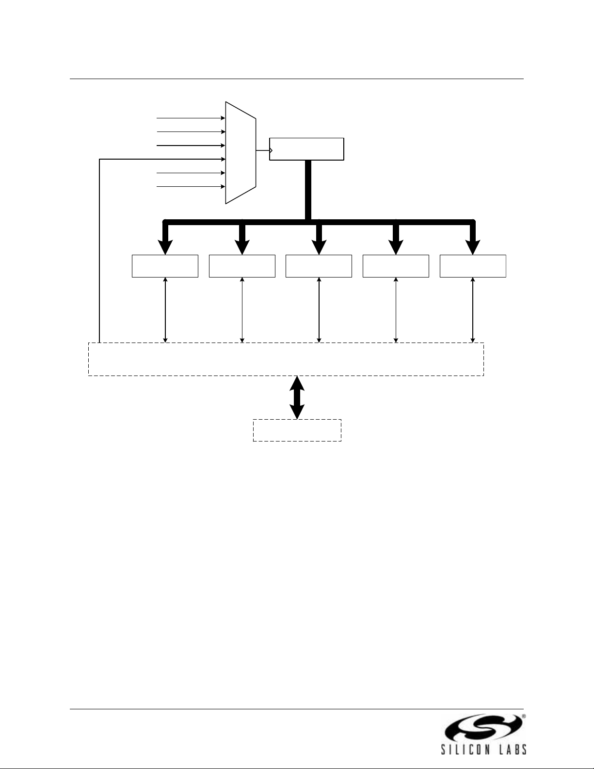
1.8. Programmable Counter Array
An on-chip Programmable Counter/Timer Array (PCA) is included in addition to the four 16-bit general purpose counter/timers. The PCA consists of a dedicated 16-bit counter/timer time base with five programmable capture/compare modules. The PCA clock is derived from one of six sources: the system clock divided
by 12, the system clock divided by 4, Timer 0 overflows, an External Clock Input (ECI), the system clock, or
the external oscilla tor c lock s ourc e di vi de d by 8 . T he ext er nal cloc k sour c e s ele ct ion is u sef ul for real - tim e
clock functional ity, where the PCA is cl ocked by an ext ernal sou rce while the int ernal osc illator d rives the
system clock.
Each capture/compare module can be configured to operate in one of six modes: Edge-Triggered Capture,
Software Timer, High Speed Output, 8- or 16-bit Pulse Width Modulator, or Frequency Output. Additionally,
Capture/Compare Module 4 offers watchdog timer (WDT) capabilities. Following a system reset, Module 4
is configured and enabled in WDT mode. The PCA Capture/Compare Module I/O and External Clock Input
may be routed to Port I/O via the Digital Crossbar.
Rev. 1.2 23
C8051F320/1
SYSCLK/12
SYSCLK/4
Timer 0 Overflow
ECI
SYSCLK
External Clock/8
PCA
CLOCK
MUX
16-Bit Counter/Timer
Capture/Compare
Module 0
ECI
CEX0
Capture/Compare
Module 1
CEX1
Capture/Compare
Module 2
CEX2
Capture/Compare
Module 3
CEX3
Capture/Compare
Module 4 / WDT
CEX4
Crossbar
Port I/O
Figure 1.9. PCA Block Diagram
1.9. 10-Bit Analog to Digital Converter
The C8051F320/1 devices inclu de an on-chip 10-bit SAR ADC with a 17-channel differential input multiplexer. With a maximum throughput of 200 ksps, th e AD C offers tru e 10 -bit l in eari ty w ith an INL of ±1LSB.
The ADC system includ es a configurable ana log multiplexer that selects both positiv e and negative ADC
inputs. Ports1-3 are available as ADC inpu ts; additional ly, the on-chip Te mperat ure Sens or outpu t and the
power supply voltage (VDD) a re avai lable as ADC inputs. Us er firm ware ma y sh ut down the A DC to s ave
power.
Conversions can be started in six ways: a software command, an overflow of Timer 0, 1, 2, or 3, or an
external convert start signal. This flexibility allows the start of conversion to be triggered by software
events, a periodic sig nal (timer ove rflows), or e xternal HW sig nals. Convers ion completi ons are ind icated
by a status bit and an interrupt (if enable d). The resulting 10-bit data word is latched into the ADC da ta
SFRs upon completion of a conversion.
Window compare registers for the ADC data can be configured to interrupt the controller when ADC data is
either within or o utside of a specified range. Th e ADC can monitor a key v oltage continuously in back
ground mode, but not interrupt the controller unless the converted data is within/outside the specified
range.
24 Rev. 1.2
P2.4-2.7
available on
C8051F320
Temp
Sensor
Analog Multiplexer
P1.0
P1.7
P2.0
P2.7
P3.0
VDD
P1.0
19-to-1
AMUX
Configuration, Control, and Data Registers
(+)
10-Bit
SAR
(-)
ADC
C8051F320/1
000 AD0BUSY (W)
Start
Conversion
16
001
010
011
100
101
Timer 0 Overflow
Timer 2 Overflow
Timer 1 Overflow
CNVSTR Input
Timer 3 Overflow
ADC Data
Registers
P2.4-2.7
available on
C8051F320
P1.7
P2.0
P2.7
P3.0
VREF
GND
19-to-1
AMUX
End of
Conversion
Interrupt
Window Compare
Logic
Window
Compare
Interrupt
Figure 1.10. 10-Bit ADC Block Diagram
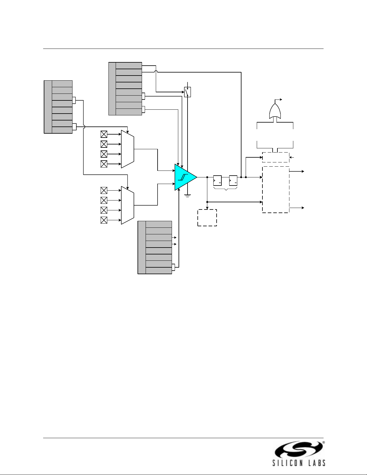
1.10. Comparators
C8051F320/1 devices include two on- chip voltage comparators tha t are enabled/disabled and configured
via user software. Port I/O pins may be configured as comparator inputs via a selection mux. Two compar
ator outputs may be routed to a Port pin if desired: a latched out put and/or an unlatch ed (asynchronous)
output. Comparator response tim e is programmable, allowin g the user to select between hig h-speed and
low-power modes. Positive and negative hysteresis are also configurable.
Comparator interrupts may be generated on rising, falling, or both edges. When in IDLE mode, these interrupts may be used as a “wake-up” source. Comparator0 may also be configured as a reset source.
Figure 1.11 shows the Comparator0 block diagram.
-
Rev. 1.2 25
C8051F320/1
CMX0N1
CMX0N0
CPT0MX
CMX0P1
CMX0P0
P1.0
P1.4
P2.0
P2.4
P1.1
P1.5
P2.1
P2.5
CP0EN
CP0OUT
CP0RIF
CP0FIF
CP0HYP1
CPT0CN
CP0HYP0
CP0HYN1
CP0HYN0
CP0 +
CP0 -
VDD
CP0
Interrupt
CP0
Rising-edg e
Interrupt
Logic
+
-
SET
D
(SYNCHRONIZER)
SET
D
Q
Q
CLR
CLR
Q
Q
Crossbar
GND
CP0
Falling-edge
CP0RIE
CP0FIE
CP0
CP0A
Reset
Decision
Tree
Note: P2.4 and P2.5 availab le
only on C8051F320
Figure 1.11. Comparator0 Block Diagram
CP0RIE
CP0FIE
CPT0MD
CP0MD1
CP0MD0
26 Rev. 1.2
C8051F320/1
2. Absolute Maximum Ratings
Table 2.1. Absolute Maximum Ratings
Parameter Conditions Min Typ Max Units
Ambient temperature under bias
Storage Temperature –65 — 150 °C
Voltage on any Port I/O Pin or /RST with
respect to GND
Voltage on VDD with respect to GND –0.3 — 4.2 V
Maximum Total current through VDD and
GND
Maximum output current sunk by /RST or any
Port pin
Note: Stresses above tho se list ed under “Abs olute Maximum Rating s” may ca use perm anent damage to the devic e.
This is a stress rating only and f unctional operation of the d evices a t those or a ny other c onditions ab ove tho se
indicated in the o peration l istings of this spe cificati on is not implied . Exposur e to max imum rati ng condi tions for
extended periods may affect device reliability.
–55 — 125 °C
–0.3 — 5.8 V
— — 500 mA
— — 100 mA
Rev. 1.2 27
C8051F320/1
3. Global Electrical Characteristics
Table 3.1. Global Electrical Characteristics
–40 to +85 °C, 25 MHz system clock unless otherwise noted.
Parameter Conditions Min Typ Max Units
1,2
Digital Supply Voltage
Digital Supply RAM Data
V
RST
- 1.5 — V
Retention Voltage
SYSCLK (System Clock)
T
(SYSCLK High Ti me)
SYSH
T
(SYSCLK Low Time)
SYSL
Specificed Operating Tem-
3
0 — 25 MHz
18 — — ns
18 — — ns
–40 — +85 °C
perature Range
Digital Supply Current - CPU Active (Normal Mode, fetching instructions from Flash)
IDD
4
VDD = 3.6 V; F = 25 MHz — 12.3 13.6 mA
VDD = 3.3 V, F = 24 MHz — 10.6 11.5 mA
VDD = 3.3 V, F = 6 MHz — 3.2 — mA
VDD = 3.3 V, F = 32 kHz — 38 — uA
VDD = 3.0 V, F = 24 MHz — 9.0 9.8 mA
VDD = 3.0 V, F = 6 MHz — 2.7 — mA
VDD = 3.0 V, F = 32 kHz — 32 — uA
IDD Supply Sensitivity
4
F = 24 MHz — 0.66 — %/V
F = 6 MHz — 0.63 — %/V
4,5
IDD Frequency Sensitivity
VDD = 3.0 V, F < 15 MHz, T = 25 °C — 0.45 — mA/MHz
VDD = 3.0 V, F > 15 MHz, T = 25 °C — 0.26 — mA/MHz
VDD = 3.3 V, F < 15 MHz, T = 25 °C — 0.53 — mA/MHz
VDD = 3.3 V, F > 15 MHz, T = 25 °C — 0.29 — mA/MHz
Digital Supply Current - CPU and USB Active (USB Transceiver Enabled and Connected to PC)
IDD
4
VDD = 3.3 V, F = 24 MHz, Full Speed — 16.8 — mA
VDD = 3.0 V, F = 24 MHz, Full Speed — 14.4 — mA
VDD = 3.3 V, F = 6 MHz, Low Speed — 7.2 — mA
VDD = 3.0 V, F = 6 MHz, Low Speed — 6.0 — mA
3.0 3.6 V
Digital Supply Current - CPU Inactive (Idle Mode, not fetching instructions from Flash)
IDD
4
VDD = 3.6 V; F = 25 Mhz — 5.8 6.5 mA
VDD = 3.3 V, F = 24 MHz — 5.2 5.9 mA
VDD = 3.3 V, F = 6 MHz — 1.7 — mA
VDD = 3.3 V, F = 32 kHz — 14 — uA
VDD = 3.0 V, F = 24 MHz — 4.6 5.2 mA
VDD = 3.0 V, F = 6 MHz — 1.5 — mA
VDD = 3.0 V, F = 32 kHz — 11 — uA
28 Rev. 1.2
C8051F320/1
Table 3.1. Global Electrical Characteristics (Continued)
–40 to +85 °C, 25 MHz system clock unless otherwise noted.
Parameter Conditions Min Typ Max Units
IDD Supply Sensitivity
IDD Frequency Sensitivity
4
4,6
VDD = 3.0 V, F < 1 MHz, T = 25 °C — 0.25 — mA/MHz
VDD = 3.0 V, F > 1 MHz, T = 25 °C — 0.17 — mA/MHz
VDD = 3.3 V, F < 1 MHz, T = 25 °C — 0.29 — mA/MHz
VDD = 3.3 V, F > 1 MHz, T = 25 °C — 0.20 — mA/MHz
Digital Supply Current
(Stop Mode)
Notes:
1. Given in Table 10.1, “Reset Electrical Characteristics,” on page 104.
2. USB requires a minimum supply voltage of 3.0 V.
3. SYSCLK must be at least 32 kHz to enable debugging.
4. Based on device characterization data; Not production tested.
5. IDD can be estimated for frequencies < 15 MHz by simply multiplying the frequency of interest by the
frequency sensitivity number for that range. When using these numbers to estimate IDD for >15
estimate should b e the cur rent at 24
number. For example: VDD
20 MHz) x 0.26 mA/MHz = 7.96 mA.
6. Idle IDD can be estimated for frequencies < 1 MHz by simply multiplying the frequency of interest by the
frequency sensitivity number for that range. When using these numbers to estimate Idle IDD for >1
estimate should b e the cur rent at 24
number. For example: VDD
5 MHz) x 0.17 mA/MHz = 1.37 mA.
= 3.0 V; F = 20 MHz, IDD = 9.0 mA – (24 MHz –
= 3.0 V; F = 5 MHz, Idle IDD = 4.6 mA – (24 MHz –
F = 24 MHz — 0.47 — %/V
F = 6 MHz — 0.50 — %/V
Oscillator not running,
Monitor disabled
V
DD
MHz minus the d if fere nce i n curre nt ind icated by th e frequ ency sens itivit y
MHz minus the d if fere nce i n curre nt ind icated by th e frequ ency sens itivit y
— <0.1 — uA
MHz, the
MHz, the
Table 3.2. Index to Electrical Characteristics Tables
Peripheral Electrical Characteristics Page #
ADC0 Electrical Characteristics
Voltage Reference Electrical Characteristics
Comparator Electrical Characteristics
Voltage Regulator Electrical Characteristics
Reset Electrical Characteristics
Flash Electrical Characteristics
Internal Oscillato r Elec tri cal Char ac teri st ic s
Port I/O DC Electrical Characteristics
53
55
65
67
104
106
124
137
Rev. 1.2 29
C8051F320/1
4. Pinout and Package Definitions
Table 4.1. Pin Definitions for the C8051F320/1
Name
VDD 6 6
GND 3 3 Ground.
/RST/
C2CK
P3.0/
C2D
REGIN
VBUS 8 8 D In
D+ 4 4 D I/O USB D+.
D- 5 5 D I/O USB D–.
P0.0 2 2 D I/O Port 0.0. See Section 14 for a complete description of Port 0.
P0.1 1 1 D I/O Port 0.1.
P0.2/
Pin Numbers
‘F320 ‘F321
9 9
10 10
7 7
Type Description
Power In
Power
Out
D I/O
D I/O
D I/O
D I/O
Power In 5 V Regulator Input. This pin is the input to the on-chip volt-
D I/O
2.7-3.6 V Power Supply Voltage Input.
3.3 V Voltage Regulator Output. See Section 8.
Device Reset. Open-drain output of internal POR or VDD
monitor. An external source can initiate a system reset by
driving this pin low for at least 15
Clock signal for the C2 Debug Interface.
Port 3.0. See Section 14 for a complete description.
Bi-directional data signal for the C2 Debug Interface.
age regulator.
VBUS Sense Input. This pin should be connected to the
VBUS signal of a USB network. A 5
cates a USB network connection.
Port 0.2.
µs. S ee Section 10.
V signal on this pin indi-
32 28
XTAL1
P0.3/
31 27
XTAL2
P0.4 30 26 D I/O Port 0.4.
P0.5 29 25 D I/O Port 0.5.
P0.6/
28 24
CNVSTR
P0.7/
27 23
VREF
P1.0 26 22
30 Rev. 1.2
A In
D I/O
A I/O or
D In
D I/O
A I/O
D I/O or
A In
External Clock Input. This pin is the external oscillator return
for a crystal or resonator. See
Port 0.3.
External Clock Output. This pin is the excitation driver for an
external crystal or resonator, or an external clock input for
CMOS, capacitor, or RC oscillator configurations. See
tion 13.
Port 0.6.
ADC0 External Convert Start Input. See Section 5.
Port 0.7.
External VREF input or output. See Section 6.
Port 1.0. See Section 14 for a complete description of Port 1.
Section 13.
Sec-

C8051F320/1
Table 4.1. Pin Definitions for the C8051F320/1 (Continued)
Name
P1.1 25 21
P1.2 24 20
P1.3 23 19
P1.4 22 18
P1.5 21 17
P1.6 20 16
P1.7 19 15
P2.0 18 14
P2.1 17 13
P2.2 16 12
P2.3 15 11
P2.4 14
P2.5 13
P2.6 12
P2.7 11
Pin Numbers
‘F320 ‘F321
Type Description
D I/O or
A In
D I/O or
A In
D I/O or
A In
D I/O or
A In
D I/O or
A In
D I/O or
A In
D I/O or
A In
D I/O or
A In
D I/O or
A In
D I/O or
A In
D I/O or
A In
D I/O or
A In
D I/O or
A In
D I/O or
A In
D I/O or
A In
Port 1.1.
Port 1.2.
Port 1.3.
Port 1.4.
Port 1.5.
Port 1.6.
Port 1.7.
Port 2.0. See Section 14 for a complete description of Port 2.
Port 2.1.
Port 2.2.
Port 2.3.
Port 2.4.
Port 2.5.
Port 2.6.
Port 2.7.
Rev. 1.2 31

C8051F320/1
P0.2
32
P0.3
31
P0.4
30
P0.5
29
P0.6
28
P0.7
27
P1.0
26
P1.1
25
P0.1
P0.0
GND
D-
VDD
REGIN
VBUS
1
2
3
4
5
6
7
8
9
/RST / C2CK
C8051F320
Top View
10
11
12
P2.6
P2.7
P3.0 / C2D
13
P2.5
14
P2.4
15
P2.3
16
P2.2
24
23
22
21
20
19
18
17
P1.2
P1.3
P1.4
P1.5D+
P1.6
P1.7
P2.0
P2.1
Figure 4.1. LQFP-32 Pinout Diagram (Top View)
32 Rev. 1.2

C8051F320/1
Figure 4.2. LQFP-32 Package Diagram
Table 4.2. LQFP-32 Package Dimensions
Dimension Min Nom Max Dimension Min Nom Max
A - - - - - - 1.60 E 9.00 BSC.
A1 0.05 - - - 0.15 E1 7.00 BSC.
A2 1.35 1.40 1.45 L 0.45 0.60 0.75
b 0.30 0.37 0.45 aaa 0.20
c 0.09 - - - 0.20 bbb 0.20
D 9.00 BSC. ccc 0.10
D1 7.00 BSC. ddd 0.20
e 0.80 BSC. θ 0° 3.5° 7°
Notes:
1. All dimensions shown are in millimeters (mm) unless otherwise noted.
2. Dimensioning and Tolerancing per ANSI Y14.5M-1994.
3. This drawing conforms to JEDEC outline MS-026, variation BBA.
4. Recommended card reflow profile is per the JEDEC/IPC J-STD-0 20C specifica tion for Small Body
Components.
Rev. 1.2 33

C8051F320/1
GND
P0.1
P0.0
GND
D+
D-
VDD
REGIN
P0.2
28
1
2
3
P0.3
27
P0.4
26
P0.5
25
P0.6
24
P0.7
23
P1.0
22
21
20
19
P1.1
P1.2
P1.3
C8051F321
4
18
P1.4
Top View
5
6
GND
7
17
16
15
P1.5
P1.6
P1.7
8
VBUS
9
/RST / C2CK
10
P3.0 / C2D
11
P2.3
Figure 4.3. QFN-28 Pinout Diagram (Top View)
34 Rev. 1.2
12
P2.2
13
P2.1
14
P2.0

C8051F320/1
Figure 4.4. QFN-28 Package Drawing
Dimension Min Nom Max Dimension Min Nom Max
A 0.80 0.90 1.00 E2 2.90 3.15 3.35
A1 0.03 0.07 0.11 L 0.45 0.55 0.65
A3 0.25 REF aaa 0.15
b 0.18 0.25 0.30 bbb 0.10
D 5.00 BSC. ddd 0.05
D2 2.90 3.15 3.35 eee 0.08
e 0.50 BSC. Z 0.435
E 5.00 BSC. Y 0.18
Notes:
1. All dimensions shown are in millimeters (mm) unless otherwise noted.
2. Dimensioning and Tolerancing per ANSI Y14.5M-1994.
3. This drawing conforms to JEDEC outline MO-243, variation VHHD except for custom features D2,
E2, L, Z, and Y which are toleranced per supplier designation.
4. Recommended card reflow profile is per the JEDEC/ IPC J-STD-02 0C speci fication for Small Body
Components.
Table 4.3. QFN-28 Package Dimensions
Rev. 1.2 35
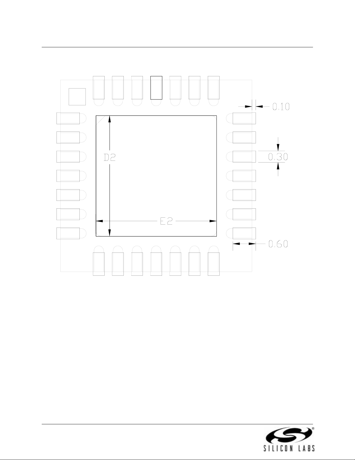
C8051F320/1
Figure 4.5. Typical QFN-28 Landing Diagram
36 Rev. 1.2

C8051F320/1
Figure 4.6. QFN-28 Solder Paste Recommendation
Rev. 1.2 37

C8051F320/1
5. 10-Bit ADC (ADC0)
The ADC0 subsystem for the C8 051F3 20/1 co nsists of two anal og mult iplex ers (refe rred to coll ectivel y as
AMUX0) with 17 total input selections, and a 200
integrated track-and- hold and prog rammable window de tector. The AMUX0, data conversion modes, an d
window detector are all configurable under so ftware control via the Special Function Regi sters shown in
Figure 5.1. ADC0 operates in both Sin gle-ended and Differential modes, and may be configured to measure P1.0-P3.0, the Temperature Sensor output, or VDD with respect to P1.0 -P3.0, VREF, or GND. The
ADC0 subsystem is enabled only when the AD0EN bit in the ADC0 Control register (ADC0C N) is set to
logic
1. The ADC0 subsystem is in low power shutdown when this bit is logic 0.
ksps, 10-bit successive-approximation-register ADC with
P2.4-2.7
available on
C8051F320
Temp
Sensor
P2.4-2.7
availabl e o n
C8051F320
P1.0
P1.7
P2.0
P2.7
P3.0
VDD
P1.0
P1.7
P2.0
P2.7
P3.0
VREF
GND
19-to-1
AMUX
AMX0P
AMX0P4
AMX0P3
AMX0P2
AMX0P1
AMX0P0
VDD
(+)
10-Bit
AD0EN
ADC0CN
AD0TM
AD0INT
AD0BUSY
SAR
19-to-1
AMUX
AMX0N
AMX0N4
(-)
AD0SC2
AD0SC3
AMX0N3
AMX0N2
AD0SC4
AMX0N1
AMX0N0
ADC0CF
AD0SC1
AD0SC0
AD0LJST
ADC
ADC0LTH
ADC0GTH ADC0GTL
REF
SYSCLK
ADC0LTL
Figure 5.1. ADC0 Functional Block Diagram
AD0CM1
AD0CM2
AD0WINT
Start
Conversion
AD0CM0
000 AD0BUSY (W)
Timer 0 Overflow
001
Timer 2 Overflow
010
Timer 1 Overflow
011
100
CNVSTR Input
101 Timer 3 Overflow
ADC0L
ADC0H
AD0WINT
Window
Compare
32
Logic
38 Rev. 1.2

C8051F320/1
5.1. Analog Multiplexer
AMUX0 selects the positiv e and negative inpu ts to the ADC. Any of the foll owing may be selec ted as the
positive input: P 1.0-P3.0, t he on-chip temperature s ensor, or the positive power sup ply (V
following may be selecte d as the negative input: P1.0-P3. 0, VREF, or GND. When GND is selected as
the negative input, ADC0 operates in Single-ended Mode; all other times, ADC0 operates in Differ
ential Mode. The ADC0 inpu t cha nnels are s elec ted in the AMX0 P and AMX 0N r egist ers as des cribed in
Figure 5.2 and Figure 5.2.
The conversion code forma t differs between Single-ended and Differen tial modes. The registers ADC0 H
and ADC0L contain the high and low bytes of the ou tput conver sion cod e from the ADC at the comple tion
of each conversion. Data can be right-justified or left-justified, depending on the setting of the AD0LJST bit
(ADC0CN.0). When in Single-ended Mode, conversion codes are represented as 10-bit unsigned integers.
Inputs are measured from ‘ 0’ to VREF x 1 023/1024. Exampl e codes are sho wn below for bo th right-justi
fied and left-justified data. Unused bits in the ADC0H and ADC0L registers are set to ‘0’.
). Any of the
DD
-
-
Input Voltage
(Single-Ended)
VREF x 1023/1024 0x03FF 0xFFC0
VREF x 512/1024 0x0200 0x8000
VREF x 256/1024 0x0100 0x4000
0 0x0000 0x0000
When in Differential Mo de, conversi on codes are r epresented as 10-bit signe d 2’s complement numbers.
Inputs are measured from –V RE F to VRE F x 511/512. Example co des a re s how n be lo w fo r both r ight- ju s
tified and left-justified data. For right-justified data, the unused MSBs of ADC0H are a sign-extension of the
data word. For left-justified data, the unused LSBs in the ADC0L register are set to ‘0’.
Input Voltage
(Differential)
VREF x 511/512 0x01FF 0x7FC0
VREF x 256/512 0x0100 0x4000
0 0x0000 0x0000
–VREF x 256/512 0xFF00 0xC000
–VREF 0xFE00 0x8000
Important Note About ADC0 Input Configuration: Port pins selected as ADC0 inputs s hould be c onfigured as analog inpu ts, and should be skipped by the Di gital Crossbar. To con figure a Por t pin for analog
input, set to ‘0’ the corresp onding b it in r egister Pn MDIN (for n = 0,1,2,3 ). To force the Crossbar to skip a
Port pin, set to ‘1’ the corresponding bit in register PnSKIP (for n = 0,1,2). See
put” on page 125 for more Port I/O configuration details.
Right-Justified ADC0H:ADC0L
(AD0LJST = 0)
Right-Justified ADC0H:ADC0L
(AD0LJST = 0)
Left-Justified ADC0H:ADC0L
(AD0LJST = 1)
Left-Justified ADC0H:ADC0L
(AD0LJST = 1)
Section “14. Port Input/Out-
-
Rev. 1.2 39

C8051F320/1
5.2. Temperature Sensor
The temperature sensor transfer function is shown in Figure 5.2. The output voltage (V
ADC input when th e temperatur e sensor is selected by bits AM X0P4-0 in register AM X0P. Values for the
Offset and Slope parameters can be found in
V
= (Gain x TempC) + Offset
TEMP
Temp
= (V
C
Table 5.1.
- Offset) / Gain
TEMP
) is the positive
TEMP
Gain (V / deg C)
Voltage
Offset (V at 0 Celsius)
Temperature
Figure 5.2. Temperature Sensor Transfer Function
The uncalibrated temperat ure sen sor output is extremel y linear and suitable for relativ e temper ature measurements (see Table 5.1 for linearity specifications). For absolute temperature measurements, offset and/
or gain calibration is recommended. Typically a 1-point (offset) calibration includes the following steps:
Step 1. Control/measure the ambient temperature (this temperature must be known).
Step 2. Power the device, and delay for a few seconds to allow for self-heating.
Step 3. Perform an ADC conversion with the temperature sensor selected as the positive input
and GND selected as the negative input.
Step 4. Calculate the offset characteristics, and store this value in non-volatile memory for use
with subsequent temperature sensor measurements.
Figure 5.3 shows the typical temperature sensor error assuming a 1-point calibration at 25 °C. Note that
parameters which affect ADC measurement, in particular the voltage reference value, will also
affect temperature measurement.
40 Rev. 1.2

C8051F320/1
0
0
0
0
0
5.0
0
4.0
0
3.0
0
2.0
0
1.0
0
0.0
0
-40.00 -20.00
-1.00
Error (degrees C)
-2.00
-3.00
-4.00
-5.00
0.0
0
20.0
0
Temperature (degrees C)
40.0
0
60.0
0
80.0
0
5.0
0
4.0
0
3.0
0
2.0
0
1.0
0
0.0
0
-1.0
-2.0
-3.0
-4.0
-5.0
Figure 5.3. Temperature Sensor Error with 1-Point Calibration (VREF = 2.40 V)
Rev. 1.2 41

C8051F320/1
5.3. Modes of Operation
ADC0 has a maximum c onversion s peed of 200 ksps. The ADC0 conversion clock is a divided version of
the system clock, determined by the AD0SC bits in the ADC0CF register (system clock divided by
(AD0SC
5.3.1. Starting a Conversion
A conversion can be initia ted in one of fiv e ways, depen ding on the program med states of the ADC0 Start
of Conversion Mode bits (AD0CM2–0) in register ADC0CN. Conversions may be initiated by one of the fol
lowing:
Writing a ‘1’ to AD0BUSY p rovides software contr ol of ADC0 whereby conversions are perfor med "ondemand". During conversion, the AD0BUSY bit is set to logic 1 and reset to logic 0 when the conversion is
complete. The falling edge of A D0BUSY trigger s an inter rupt (wh en enab led) a nd sets the ADC0 i nterrup t
flag (AD0INT). Note: When polling for ADC conversion completions, the ADC0 interrupt flag (AD0INT)
should be used. Converted data is available in the ADC0 data registers, ADC0H:ADC0L, when bit AD0INT
is logic 1. Note that when Timer 2 or Timer 3 overflows are used as the conversion source, Low Byte over
flows are used if Timer 2/3 is in 8-bit mode; High byte overflows are used if Timer 2/3 is in 16-bit mode. See
Section “19. Timers” on page 209 for timer configuration.
+ 1) for 0 ≤ AD0SC ≤ 31).
-
1. Writing a ‘1’ to the AD0BUSY bit of register ADC0CN
2. A Timer 0 overflow (i.e., timed continuous conversions)
3. A Timer 2 overflow
4. A Timer 1 overflow
5. A rising edge on the CNVSTR input signal (pin P0.6)
6. A Timer 3 overflow
-
Important Note About Using CNVSTR: The CNVSTR input pin also functions as Port pin P0.6. When the
CNVSTR input is used as the ADC0 c onversion source, P ort pin P0.6 should be skipped by th e Digital
Crossbar. To configure the Crossbar to skip P0.6 , set to ‘1’ Bit6 i n register P 0SKIP. See
Input/Output” on page 125 for details on Port I/O configuration.
Section “14. Port
42 Rev. 1.2

C8051F320/1
(
5.3.2. Tracking Modes
The AD0TM bit in register ADC0CN controls the ADC0 track-and-hold mode. In its default state, the ADC0
input is continuous ly tracked, except when a conversion is in prog ress. When the AD0TM bit is logic 1,
ADC0 operates in low-power track-and-ho ld mode. In this mode, ea ch convers ion is preceded by a trac k
ing period of 3 SAR clo cks (after the start-of-c onversion sig nal). When th e CNVSTR signal is used to initiate conversions in l ow-power tracking mode, A DC0 tr ack s o nly wh en CNV S TR is lo w; co nv er sion begi ns
on the rising edge of CNVSTR (see
is in low power standby or sleep mo des. Low -power tr ack-and- hold mode i s also u seful wh en AMUX settings are frequently ch anged, due to the settling time requirements descr ibed in Section “5.3.3. Settling
Time Requirements” on page 44.
CNVSTR
(AD0CM[2:0] = 100)
Figure 5.4). Tracking can also be disabled (shutdown) when the device
A. ADC0 Timing for External Trigger Source
-
SAR Clocks
AD0TM = 1
Write '1' to AD0BUSY,
Timer 0, Timer 2,
Timer 1, Timer 3 Overflow
AD0CM[2:0] = 000, 001,010
011, 101)
SAR
Clocks
AD0TM = 1
SAR
Clocks
AD0TM = 0
Low Power
or Convert
Track or Convert Convert TrackAD0TM = 0
123456789
Track Convert
10 11
B. ADC0 Timing for Internal Trigger Source
Low Power
or Convert
Track or
Convert
123456789101112
Track Convert Low Power Mode
123456789
Convert Track
10
11
13 14
12 13 14
15 16 17
12 13 14
Low Power
Mode
Figure 5.4. 10-Bit ADC Track and Conversion Example Timing
Rev. 1.2 43

C8051F320/1
5.3.3. Settling Time Requirements
When the ADC0 input confi guration is changed (i.e., a di fferent AMUX0 selection is made), a minimum
tracking time is required before an accurate conversion can be performed. This tracking time is determined
by the AMUX0 resistance, the A DC0 sa mpl in g ca pacitanc e, any ex ter nal sou rce re sis tance, and the acc u
racy required for the conv ersion. Note that in low-power tracking mode, th ree SAR clocks are used for
tracking at the start of every conve rsi on. F or mos t app li ca tio ns, these three SAR clocks will meet th e min i
mum tracking time requirements.
Figure 5.5 shows the equivalent A DC0 input circ uits for both D ifferential and S ingle-ended modes. Noti ce
that the equivalent time c onstant f or both inp ut circu its is the same . The req uired ADC0 settling time for a
given settling accuracy (SA) may be approximated by
Sensor output or VDD with respec t to GND, R
TOTAL
settling time requirements.
Equation 5.1. ADC0 Settling Time Requirements
n
2
⎛⎞
t
Where:
SA is the settling accuracy, given as a fraction of an LSB (for example, 0.25 to settle within 1/4 LSB)
t is the required settling time in seconds
R
n is the ADC resolution in bits (10).
is the sum of the AMUX0 resistance and any external source resistance.
TOTAL
------ -
×ln=
⎝⎠
SA
R
Equation 5.1. When measuring the Temperature
reduces to R
TOTALCSAMPLE
. See Table 5.1 for ADC0 minimum
MUX
-
-
Differential Mode
MUX
Select
Px.x
RC
= R
Input
MUX
Px.x
MUX Select
Single-Ended Mode
MUX Select
R
* C
R
MUX
MUX
= 5k
SAMPLE
= 5k
C
SAMPLE
C
SAMPLE
= 5pF
= 5pF
Px.x
RC
Input
= R
MUX
R
* C
MUX
= 5k
SAMPLE
Figure 5.5. ADC0 Equivalent Input Circuits
C
SAMPLE
= 5pF
44 Rev. 1.2
C8051F320/1
SFR Definition 5.1. AMX0P: AMUX0 Positive Channel Select
R R R R/W R/W R/W R/W R/W Reset Value
- - - AMX0P4 AMX0P3 AMX0P2 AMX0P1 AMX0P0 00000000
Bit7 Bit6 Bit5 Bit4 Bit3 Bit2 Bit1 Bit0 SFR Address:
Bits7–5: UNUSED. Read = 000b; Write = don’t care.
Bits4–0: AMX0P4–0: AMUX0 Positive Input Selection
AMX0P4–0 ADC0 Positive Input
00000 P1.0
00001 P1.1
00010 P1.2
00011 P1.3
00100 P1.4
00101 P1.5
00110 P1.6
00111 P1.7
01000 P2.0
01001 P2.1
01010 P2.2
01011 P2.3
01100* P2.4*
01101* P2.5*
01110* P2.6*
01111* P2.7*
10000 P3.0
10001–11101 RESERVED
1111 0 Temp Sensor
11111 VDD
*Note: Only applies to C8051F320; selection RESERVED on
C8051F321 devices.
0xBB
Rev. 1.2 45
C8051F320/1
SFR Definition 5.2. AMX0N: AMUX0 Negative Channel Select
R R R R/W R/W R/W R/W R/W Reset Value
- - - AMX0N4 AMX0N3 AMX0N2 AMX0N1 AMX0N0 00000000
Bit7 Bit6 Bit5 Bit4 Bit3 Bit2 Bit1 Bit0 SFR Address:
Bits7–5: UNUSED. Read = 000b; Write = don’t care.
Bits4–0: AMX0N4–0: AMUX0 Negative Input Selection.
Note that when GND is selected as the Negative Input, ADC0 operates in Single-ended
mode. For all other Negative Input selections, ADC0 operates in Differential mode.
AMX0N4–0 ADC0 Negative Input
00000 P1.0
00001 P1.1
00010 P1.2
00011 P1.3
00100 P1.4
00101 P1.5
00110 P1.6
00111 P1.7
01000 P2.0
01001 P2.1
01010 P2.2
01011 P2.3
01100* P2.4*
01101* P2.5*
01110* P2.6*
01111* P2.7*
10000 P3.0
10001–11101 RESERVED
11110 VREF
11111 GND (ADC in Single-Ended Mode)
*Note: Only applies to C8051F320; selection RESERVED on
C8051F321 devices.
0xBA
46 Rev. 1.2

C8051F320/1
A
SYSCLK
SAR
1
SFR Definition 5.3. ADC0CF: ADC0 Configuration
R/W R/W R/W R/W R/W R/W R/W R/W Reset Value
AD0SC4 AD0SC3 AD0SC2 AD0SC1 AD0SC0 AD0LJST - - 11111000
Bit7 Bit6 Bit5 Bit4 Bit3 Bit2 Bit1 Bit0 SFR Address:
0xBC
Bits7–3: AD0SC4–0: ADC0 SAR Conversion Clock Period Bits.
SAR Conversion clock is derived from system clock by the following equation, where
AD0SC refers to the 5-bit value held in bits AD0SC4-0. SAR Conversion clock requirements
are given in Table 5.1.
D0SC
Bit2: AD0LJST: ADC0 Left Justify Select.
0: Data in ADC0H:ADC0L registers are right-justified.
1: Data in ADC0H:ADC0L registers are left-justified.
Bits1–0: UNUSED. Read = 00b; Write = don’t care.
--------------------- -
CLK
–=
SFR Definition 5.4. ADC0H: ADC0 Data Word MSB
R/W R/W R/W R/W R/W R/W R/W R/W Reset Value
00000000
Bit7 Bit6 Bit5 Bit4 Bit3 Bi t2 Bit1 Bit0 SFR Address:
Bits7–0: ADC0 Data Word High-Order Bits.
For AD0LJST = 0: Bits 7-2 are the sign extension of Bit1. Bits 1–0 are the upper 2 bits of the
10-bit ADC0 Data Word.
For AD0LJST = 1: Bits 7–0 are the most-significant bits of the 10-bit ADC0 Data Word.
0xBE
SFR Definition 5.5. ADC0L: ADC0 Data Word LSB
R/W R/W R/W R/W R/W R/W R/W R/W Reset Value
00000000
Bit7 Bit6 Bit5 Bit4 Bit3 Bit2 Bit1 Bit0 SFR Address:
0xBD
Bits7–0: ADC0 Data Word Low-Order Bits.
For AD0LJST = 0: Bits 7–0 are the lower 8 bits of the 10-bit Data Word.
For AD0LJST = 1: Bits 7–6 are the lower 2 bits of the 10-bit Data Word. Bits 5–0 will always
read ‘0’.
Rev. 1.2 47

C8051F320/1
SFR Definition 5.6. ADC0CN: ADC0 Control
R/W R/W R/W R/W R/W R/W R/W R/W Reset Value
AD0EN AD0TM AD0INT AD0BUSY AD0WINT AD0CM2 AD0CM1 AD0CM0 00000000
Bit7 Bit6 Bit5 Bit4 Bit3 Bi t2 Bit1 Bit0 SFR Address:
(bit addressable)
Bit7: AD0EN: ADC0 Enable Bi t.
0: ADC0 Disabled. ADC0 is in low-power shutdown.
1: ADC0 Enabled. ADC0 is active and ready for data conversions.
Bit6: AD0TM: ADC0 Track Mode Bit.
0: Normal Track Mode: When ADC0 is enabled, tracking is continuous unless a conversion
is in progress.
1: Low-power Track Mode: Tracking Defined by AD0CM2-0 bits (see below).
Bit5: AD0INT: ADC0 Conversion Complete Interrupt Flag.
0: ADC0 has not completed a data conversion since the last time AD0INT was cleared.
1: ADC0 has completed a data conversion.
Bit4: AD0BUSY: A DC0 Busy Bit.
Read:
0: ADC0 conversion is complete or a conversion is not currently in progress. AD0INT is set
to logic 1 on the falling edge of AD0BUSY.
1: ADC0 conversion is in progress.
Write:
0: No Effect.
1: Initiates ADC0 Conversion if AD0CM2–0 = 000b
Bit3: AD0WINT: ADC0 Window Compare Interrupt Flag.
0: ADC0 Window Comparison Data match has not occurred since this flag was last cleared.
1: ADC0 Window Comparison Data match has occurred.
Bits2–0: AD0CM2–0: ADC0 Start of Conversion Mode Select.
When AD0TM = 0:
000: ADC0 conversion initiated on every write of ‘1’ to AD0BUSY.
001: ADC0 conversion initiated on overflow of Timer 0.
010: ADC0 conversion initiated on overflow of Timer 2.
011: ADC0 conversion initiated on overflow of Timer 1.
100: ADC0 conversion initiated on rising edge of external CNVSTR.
101: ADC0 conversion initiated on overflow of Timer 3.
11x: Reserved.
When AD0TM = 1:
000: Tracking initiated on write of ‘1’ to AD0BUSY and lasts 3 SAR clocks, followed by conversion.
001: Tracking initiated on overflow of Timer 0 and lasts 3 SAR clocks, followed by conversion.
010: Tracking initiated on overflow of Timer 2 and lasts 3 SAR clocks, followed by conversion.
011: Tracking initiated on overflow of Timer 1 and lasts 3 SAR clocks, followed by conversion.
100: ADC0 tracks only when CNVSTR input is logic low; conversion starts on rising CNVSTR
edge.
101: Tracking initiated on overflow of Timer 3 and lasts 3 SAR clocks, followed by conversion.
11x: Reserved.
0xE8
48 Rev. 1.2

C8051F320/1
5.4. Programmable Window Detector
The ADC Programm able Window Detector continuously com pares the ADC0 conversi on results to userprogrammed limits, and noti fies the s ystem when a de sired cond ition is dete cted. Thi s is espec ially effec
tive in an interr upt-driven system, saving code space and CPU bandwidth while delivering fast er system
response times. The win dow detector interrupt flag (AD0WINT in register ADC0C N) can also be used in
polled mode. The ADC0 Greater-Than (ADC0GTH, ADC0GTL) and Less-Than (ADC0LTH, ADC0LTL) reg
isters hold the compariso n values. The window detec tor flag can be programme d to indicate when mea sured data is inside or outside of the user-progr ammed limits, depending on the contents of the ADC0
Less-Than and ADC0 Greater-Than registers.
The Window Detector registers must be w ritten with t he same f ormat (left/ right justi fied, si gned/unsign ed)
as that of the current ADC configuration (left/right justified, single-ended/differential).
SFR Definition 5.7. ADC0GTH: ADC0 Greater-Than Data High Byte
R/W R/W R/W R/W R/W R/W R/W R/W Reset Value
11111111
Bit7 Bit6 Bit5 Bit4 Bit3 Bit2 Bit1 Bit0 SFR Address:
0xC4
-
-
Bits7–0: High byte of ADC0 Greater-Than Data Word.
SFR Definition 5.8. ADC0GTL: ADC0 Greater-Than Data Low Byte
R/W R/W R/W R/W R/W R/W R/W R/W Reset Value
Bit7 Bit6 Bit5 Bit4 Bit3 Bit2 Bit1 Bit0 SFR Addres s:
Bits7–0: Low byte of ADC0 Greater-Than Data Word.
11111111
0xC3
Rev. 1.2 49

C8051F320/1
SFR Definition 5.9. ADC0LTH: ADC0 Less-Than Data High Byte
R/W R/W R/W R/W R/W R/W R/W R/W Reset Value
Bit7 Bit6 Bit5 Bit4 Bit3 Bit2 Bit1 Bit0 SFR Address:
Bits7–0: High byte of ADC0 Less-Than Data Word.
SFR Definition 5.10. ADC0LTL: ADC0 Less-Than Data Low Byte
R/W R/W R/W R/W R/W R/W R/W R/W Reset Value
Bit7 Bit6 Bit5 Bit4 Bit3 Bit2 Bit1 Bit0 SFR Address:
00000000
0xC6
00000000
0xC5
Bits7–0: Low byte of ADC0 Less-Than Data Word.
50 Rev. 1.2

C8051F320/1
5.4.1. Window Detector In Single-Ended Mode
Figure 5.6 shows two example window comparisons for right-justified, single-ended data, with
ADC0LTH:ADC0LTL = 0x0080 ( 128d) and ADC0GTH:ADC0GTL = 0x0040 (64d). In single-ended mode ,
the input voltage can range from ‘0’ to VREF * (1023/1 024) with respec t to GND, and is re presented by a
10-bit unsigned integer v alue. In the left example, an AD0WINT interrupt will be generated if the ADC0
conversion word (ADC0H:ADC0L) is within the range defined by ADC0GTH:ADC0GTL and
ADC0LTH:ADC0LTL (if
will be generated if the ADC0 conversion word is outside of the range defined by the ADC0GT and
ADC0LT registers (if
ple using left-justified data with equivalent ADC0GT and ADC0LT register settings.
Input Voltage
(Px.x - GND)
VREF x (1023/1024)
0x0040 < ADC0H:ADC0L < 0x0080). In the right example, and AD0WINT interrupt
ADC0H:ADC0L < 0x0040 or ADC0H:ADC0L > 0x0080). Figure 5.7 shows an exam-
ADC0H:ADC0L ADC0H:ADC0L
Input Voltage
(Px.x - GND)
0x03FF
VREF x (1023/1024)
0x03FF
VREF x (128/1024)
VREF x (64/1024)
0
0x0081
0x0080
0x007F
0x0041
0x0040
0x003F
0x0000
AD0WINT
not affected
ADC0LTH:ADC0LTL
ADC0GTH:ADC0GTL
AD0WINT
not affected
AD0WINT=1
VREF x (128/1024)
VREF x (64/1024)
0
0x0081
0x0080
0x007F
0x0041
0x0040
0x003F
0x0000
ADC0GTH:ADC0GTL
AD0WINT
not affected
ADC0LTH:ADC0LTL
AD0WINT=1
AD0WINT=1
Figure 5.6. ADC Window Compare Example: Right-Justified Single-Ended Data
ADC0H:ADC0L ADC0H:ADC0L
Input Voltage
(Px.x - GND)
VREF x (1023/1024)
VREF x (128/1024)
VREF x (64/1024)
0xFFC0
0x2040
0x2000
0x1FC0
0x1040
0x1000
0x0FC0
AD0WINT
not affected
ADC0LTH:ADC0LTL
ADC0GTH:ADC0GTL
AD0WINT=1
Input Voltage
(Px.x - GND)
VREF x (1023/1024)
VREF x (128/1024)
VREF x (64/1024)
0xFFC0
0x2040
0x2000
0x1FC0
0x1040
0x1000
0x0FC0
ADC0GTH:ADC0GTL
AD0WINT
not affected
ADC0LTH:ADC0LTL
AD0WINT=1
AD0WINT
not affected
0
0x0000
0
0x0000
AD0WINT=1
Figure 5.7. ADC Window Compare Example: Left-Justified Single-Ended Data
Rev. 1.2 51

C8051F320/1
5.4.2. Window Detector In Differential Mode
Figure 5.8 shows two example window comparisons for right-justified, differential data, with
ADC0LTH:ADC0LTL = 0x004 0 (+64d) and ADC0GTH:ADC0GTH = 0xFFFF (-1d). In differential mode, the
measurable voltage between the input pins is between -VREF and VREF*(511/512). Output codes are rep
resented as 10-bit 2’s complement sign ed in tege rs. In the le ft exampl e, an AD0WINT interrupt will be generated if the ADC0 co nv ersi on wor d (ADC0H :ADC0L) is within the rang e d efin ed by A DC0GTH:ADC0GTL
and ADC0LTH:ADC0LTL (if
0xFFFF (-1d) < ADC0H:ADC0L < 0x0040 (64d)). In the right example, an
AD0WINT interrupt will be ge nerated if the ADC0 co nversion word is outside of the range defined by the
ADC0GT and ADC0LT registers (if
ADC0H:ADC0L < 0xFFFF (-1d) or ADC0H:ADC0L > 0x0040 (+64d)).
Figure 5.9 shows an example using left-justi fied data with equivalent ADC0 GT and ADC0LT register settings.
ADC0H:ADC0LADC0H:ADC0L
Input Voltage
(Px.x - Px.x)
VREF x (511/512)
0x01FF
Input Voltage
(Px.x - Px.x)
VREF x (511/512)
0x01FF
-
VREF x (64/512)
VREF x (-1/512)
-VREF
0x0041
0x0040
0x003F
0x0000
0xFFFF
0xFFFE
0x0200
AD0WINT
not affected
ADC0LTH:ADC0LTL
AD0WINT=1
ADC0GTH:ADC0GTL
AD0WINT
not affected
VREF x (64/512)
VREF x (-1/512)
-VREF
0x0041
0x0040
0x003F
0x0000
0xFFFF
0xFFFE
0x0200
ADC0GTH:ADC0GTL
AD0WINT
not affected
ADC0LTH:ADC0LTL
AD0WINT=1
AD0WINT=1
Figure 5.8. ADC Window Compare Example: Right-Justified Differential Data
ADC0H:ADC0LADC0H:ADC0L
Input Voltage
(Px.x - Px.x)
VREF x (511/512)
VREF x (64/512)
VREF x (-1/512)
0x7FC0
0x1040
0x1000
0x0FC0
0x0000
0xFFC0
0xFF80
AD0WINT
not affected
ADC0LTH:ADC0LTL
AD0WINT=1
ADC0GTH:ADC0GTL
Input Voltage
(Px.x - Px.y)
VREF x (511/512)
VREF x (64/512)
VREF x (-1/512)
0x7FC0
0x1040
0x1000
0x0FC0
0x0000
0xFFC0
0xFF80
ADC0GTH:ADC0GTL
AD0WINT
not affected
ADC0LTH:ADC0LTL
AD0WINT=1
AD0WINT
not affected
-VREF
0x8000
-VREF
0x8000
Figure 5.9. ADC Window Compare Example: Left-Justified Differential Data
52 Rev. 1.2
AD0WINT=1

C8051F320/1
Table 5.1. ADC0 Electrical Characteristics
VDD = 3.0 V, VREF = 2.40 V, –40 to +85 °C unless otherwise specified.
Parameter Conditions Min Typ Max Units
DC Accuracy
Resolution 10 bits
Integral Nonlinearity — ±0.5 ±1 LSB
Differential Nonlinearity Guaranteed Monotonic — ±0.5 ±1 LSB
Offset Error –15 0 15 LSB
Full Scale Error –15 –1 15 LSB
Offset Temperature Coefficient — 10 — ppm/°C
Dynamic Performance (10 kHz sine-wave Single-ended input, 1 dB below Full Scale, 200 ksps)
Signal-to-Noise Plus Distortion 53 55.5 — dB
Total Harmonic Distortion Up to the 5th harmonic — –67 — dB
Spurious-Free Dynamic Range — 78 — dB
Conversion Rate
SAR Conversion Clock — — 3 MHz
Conversion Time in SAR Clocks 10 — — clocks
Track/Hold Acquisit ion Time 300 — — ns
Throughput Rate — — 200 ksps
Analog Inputs
ADC Input Voltage Range Single Ended (AIN+ – GND)
Differential (AIN+ – AIN–)
Absolute Pin Voltage with respect
to GND
Input Capacitance — 5 — pF
Temperature Sensor — — —
Linearity
Gain
Offset
Power Specifications
Power Supply Current
(VDD supplied to ADC0)
Power Supply R eje ct i on — ±0.3 mV/V
Notes:
1
2
1,2
1. Includes ADC offset, gain, and linearity variations.
2. Represents one standard deviation from the mean.
Single Ended or Differential 0 — VDD V
(Temp = 0 °C) — 0.776
Operating Mode, 200 ksps — 400 900 µA
0
–VREF
— ±0.1 — °C
— 2.86 — mV/°C
— VREF
VREF
— mV
±8.5
V
V
Rev. 1.2 53
C8051F320/1
6. Voltage Reference
The Voltage reference MUX on C8051 F320/1 d evic es is confi gurable to use an exte rnally conne cted voltage reference, the internal reference voltage generator, or the power supply voltage VDD (see Figure 6.1).
The REFSL bit in the Referenc e Control regi ster (REF0CN ) selects the refer ence source. F or the inter nal
reference or an external sour ce, REFSL should be set to ‘0’; For VDD as the reference source, REFSL
should be set to ‘1’.
The BIASE bit enables the int ernal ADC bias ge nerator, which is used by th e ADC and Internal O scill ator.
This enable is forc ed to logic 1 wh en either of the afor ementioned periph erals is enabl ed. The ADC bias
generator may be enabled manually by writing a ‘1’ to the BIASE bit in register REF0CN; see
REF0CN register details. The Reference bias gene rator (see Figure 6.1) is used by the Internal Voltage
Reference, Temperature Sensor, and Clock Multiplier. The Reference bias is aut omatically enabled when
any of the aforementioned per ipherals are enabl ed. The electrical specification s for the voltage referenc e
and bias circuits are given in
Table 6.1.
Important Note About the VREF Input: Port pin P0.7 is used as the external VREF input. When using an
external voltage reference, P0.7 should be configured as analog input and skipped by the Digital Crossbar.
To con figure P0.7 as analog input, set to ‘0’ Bit7 in register P0MDIN. To configure the Crossbar to sk ip
P0.7, set to ‘1’ Bi t7 in reg ister P0SKI P. Refer to
Section “14. Port Input/Output” on page 125 for complete
Port I/O configuration details.
Figure 6.1 for
The temperature sensor connects to the ADC0 posit ive input multiplex er (see Section “5.1. Analog Multiplexer” on page 39 for details). The TEMPE bit in register REF0CN enables/disables the temperature sensor. While disabled, the temperature sensor defaults to a high impedance state and any ADC0
measurements performed on the sensor result in meaningless data.
REF0CN
BIASE
REFSL
REFBE
TEMPE
AD0EN
To ADC,
Internal Oscillator
To Analog Mux
VREF
(to ADC)
To Clock Multiplier,
Temp Sensor
VDD
GND
R1
External
Voltage
Reference
Circuit
VREF
VDD
0
1
TEMPE
IOSCEN
CLKMUL
Enable
REFBE
EN
EN
EN
ADC Bias
Temp Sensor
Reference
Bias
Internal
Reference
Figure 6.1. Voltage Reference Functional Block Diagram
54 Rev. 1.2
EN

C8051F320/1
SFR Definition 6.1. REF0CN: Reference Control
R/W R/W R/W R/W R/W R/W R/W R/W Reset Value
- - - - REFSL TEMPE BIASE REFBE 00000000
Bit7 B it6 Bit5 Bit4 B it3 Bit2 Bit1 Bi t0 SFR Address:
Bits7–3: UNUSED. Read = 00000b; Write = don’t care.
Bit3: REFSL: Voltage Reference Select.
This bit selects the source for the internal voltage reference.
0: VREF pin used as voltage reference.
1: VDD used as voltage reference.
Bit2: TEMPE: Temperature Sensor Enable Bit.
0: Internal Temperature Sensor off.
1: Internal Temperature Sensor on.
Bit1: BIASE: Internal Analog Bias Generator Enable Bit.
0: Internal Bias Generator off.
1: Internal Bias Generator on.
Bit0: REFBE: Internal Reference Buffer Enable Bit.
0: Internal Reference Buffer disabled.
1: Internal Reference Buffer enabled. Internal voltage reference driven on the VREF pin.
0xD1
Table 6.1. Voltage Reference Electrical Charac te rist ic s
VDD = 3.0 V; –40 to +85 °C unless otherwise specified.
Parameter Conditions Min Typ Max Units
Internal Reference (REFBE = 1)
Output Voltage 25 °C ambient 2.38 2.44 2.50 V
VREF Short-Circuit Current 10 mA
VREF Temperature Coeffi-
cient
Load Regulation Load = 0 to 200 µA to GND 1.5 ppm/µA
VREF Turn-on Time 1 4.7 µF tantalum, 0.1 µF ceramic bypass 2 ms
VREF Turn-on Time 2 0.1 µF ceramic bypass 20 µs
VREF Turn-on Time 3 no bypass cap 10 µs
Power Supply R eje ct i on 140 ppm/V
External Reference (REFBE = 0)
Input Voltage Range 0 VDD V
Input Current Sample Rate = 200 ksps; VREF = 3.0 V 12 µA
Bias Generators
ADC Bias Generator BIASE = ‘1’ 106 148 µA
Reference Bias Generator 42 60 µA
15 ppm/°C
Rev. 1.2 55

C8051F320/1
7. Comparators
C8051F320/1 devices i nclude tw o on-chip programmab le voltage Co mparators: Comparator0 is shown in
Figure 7.1; Comparator1 is shown in Figure 7.2. The two Comparators operate identi cally with the following exceptions: (1) Their input selections differ as shown in Figure 7.1 and Figure 7.2; (2) Comparator0 can
be used as a reset source.
Each Comparator offers programmable response time and hysteresis, an analog input multiplexer, and two
outputs that are optionally av ailable at the Port pins: a synchronous “ latched” output (CP0, CP1), or an
asynchronous “ra w” output (CP0A, CP1A). The asyn chronous signal is availabl e even when the system
clock is not active. This allows the Comparators to operate and generate an output with the device in
STOP mode. When assigned to a Port pin, the Comparator ou tputs may be configured as open drain or
push-pull (see
reset source (see Section “10.5. Comparator0 Reset” on page 101).
The Comparator0 inputs are selected in the CPT0MX register (Fi gure 7.2). The CMX0P1–CMX0P0 b its
select the Comparato r0 po si ti ve in put ; th e CMX0N1–CMX0N0 bits selec t the Com parator 0 ne gati ve i npu t.
The Comparator1 inputs are selected in the CPT1MX register (
select the Comparator1 positive input; the CMX1N1–CMX1N0 bits select the Comparator1 negative input.
Important Note About Comparator Inputs: The Port pins selected as Comparator inputs should be configured as analog inputs in their associated Port configuration register, and configured to be skipped by the
Crossbar (for details on Port configuration, see
Section “14.2. Port I/O I nitialization” on page 129). Comparator 0 may also be used as a
Figure 7.5). The C MX1P1–CMX1P0 bits
Section “14.3. General Purpose Port I/O” on page 131).
CMX0N1
CMX0N0
CPT0MX
CMX0P1
CMX0P0
Note: P2.4 and P2.5 available
only on C8051F320
P1.0
P1.4
P2.0
P2.4
P1.1
P1.5
P2.1
P2.5
CP0EN
CP0OUT
CP0RIF
CP0FIF
CP0HYP1
CPT0CN
CP0HYP0
CP0HYN1
CP0HYN0
CP0 +
CP0 -
CPT0MD
CP0RIE
CP0FIE
CP0MD1
CP0MD0
VDD
CP0
Interrupt
CP0
Rising-edge
Interrupt
+
-
GND
Reset
Decision
Tree
SET
SET
D
D
Q
Q
CLR
CLR
(SYNCHRONIZER)
Q
Q
Crossbar
Logic
CP0
Falling-edge
CP0RIE
CP0FIE
CP0
CP0A
Figure 7.1. Comparator0 Functional Block Diagram
56 Rev. 1.2

C8051F320/1
Comparator outputs can be polled in software, used as an interrupt source , and/or routed to a Port pin.
When routed to a Port pin, C omparator outp uts are ava ilable as ynch ronou s or sync hronous to the syste m
clock; the asyn chro nous output is avai labl e ev en in STOP m ode ( with no s ystem cloc k a ctive) . Whe n di s
abled, the Comparator output (if assigned to a Port I/O pin via the Crossbar) defaults to the logic low state,
and supply current falls to less than 100
for details on configuring Comparator outputs via the digital Crossbar. Comparator inputs can be externally
driven from –0.25
V to (VDD) + 0.25 V without damage or upset. The complete Comparator electrical spec-
ifications are given in Table 7.1.
Comparator response time may be c onfigured in software via the C PTnMD registers (see Figure 7.3 and
Figure 7.6). Selecting a longer response time reduces the Comparator supply current. See Table 7.1 for
complete timing and supply current specifications.
CP1EN
CP1OUT
CP1RIF
CP1FIF
CMX1N1
CMX1N0
CPT1MX
CMX1P1
CMX1P0
P1.2
P1.6
P2.2
P2.6
P1.3
P1.7
P2.3
P2.7
CP1HYP1
CPT1CN
CP1HYP0
CP1HYN1
CP1HYN0
nA. See Section “1 4.1. Priority Crossb ar Decoder” on page 127
VDD
CP1
Interrupt
CP1 +
CP1 -
CP1
Rising-edge
Interrupt
Logic
+
-
GND
SET
SET
Q
D
D
Q
CLR
CLR
(SYNCHRONIZER)
Q
Q
Crossbar
CP1
Falling-edge
CP1RIE
CP1FIE
CP1
CP1A
-
Note: P2.6 and P2.7 available
only on C8051F320
Figure 7.2. Comparator1 Functional Block Diagram
CP1RIE
CP1FIE
CPT1MD
CP1MD1
CP1MD0
Rev. 1.2 57

C8051F320/1
CP0+
VIN+
CP0-
VIN-
CIRCUIT CONFIGURATION
Positive Hysteresis Voltage
(Programmed with CP0HYP Bits)
VIN-
INPUTS
VIN+
OUTPUT
V
OL
Positive Hysteresis
Disabled
Figure 7.3. Comparator Hysteresis Plot
+
CP0
_
V
OH
OUT
Maximum
Positive Hysteresis
Negative Hysteresis
Disabled
Negative Hysteresis Voltag e
(Programmed by CP0HYN Bits)
Maximum
Negative Hysteresis
Comparator hysteresis is program med using Bi ts3–0 in the Comparator Contr ol Reg ister CPTnCN (shown
in
Figure 7.1 and Figure 7.4). The amount of negative hy steresis vol tage is determin ed by the setti ngs of
the CPnHYN bits. As shown in Figure 7.3, settings of 20, 10 or 5 mV of negative hysteresis can be
programmed, or negativ e hys ter es is ca n be di sa bled. In a similar way, the amount of positive hysteresis is
determined by the setting the CPnHYP bits.
Comparator interrupts can be generated on both rising-edge and falling-edge output transitions. (For Interrupt enable and priority control, see Section “9.3. Interrupt Handler” on page 86.) The CPnFIF flag is set to
‘1’ upon a Comparator fallin g-edge, and the CPnRIF flag is set to ‘1’ upo n the Comparator rising-edge.
Once set, these bits remain set until cleared by software. The output state of the Comparator can be
obtained at any time by read ing the CPn OUT bit. The Com parator is enable d by setti ng the CPnEN bit to
‘1’, and is disabled by clearing this bit to ‘0’.
58 Rev. 1.2

C8051F320/1
SFR Definition 7.1. CPT0CN: Comparator0 Control
R/W R R/W R/W R/W R/W R/W R/W Reset Value
CP0EN CP0OUT CP0RIF CP0FIF CP0HYP1 CP0HYP0 CP0HYN1 CP0HYN0 00000000
Bit7 Bit6 Bit5 Bit4 Bit3 Bit2 Bit1 Bit0 SFR Address:
0x9B
Bit7: CP0EN: Comparator0 Enable Bit.
0: Comparator0 Disabled.
1: Comparator0 Enabled.
Bit6: CP0OUT: Comparator0 Output State Flag.
0: Voltage on CP0+ < CP0–.
1: Voltage on CP0+ > CP0–.
Bit5: CP0RIF: Comparator0 Rising-Edge Flag.
0: No Comparator0 Rising Edge has occurred since this flag was last cleared.
1: Comparator0 Rising Edge has occurred.
Bit4: CP0FIF: Comparator0 Fallin g- Ed ge Flag.
0: No Comparator0 Falling-Edge has occurred since this flag was last cleared.
1: Comparator0 Falling-Edge Interrupt has occurred.
Bits3–2: CP0HYP1–0: Comparator0 Positive Hysteresis Control Bits.
00: Positive Hysteresis Disabled.
01: Positive Hysteresis = 5 mV.
10: Positive Hysteresis = 10 mV.
11: Positive Hysteresis = 20 mV.
Bits1–0: CP0HYN1–0: Comparator0 Negative Hysteresis Control Bits.
00: Negative Hysteresis Disabled.
01: Negative Hysteresis = 5 mV.
10: Negative Hysteresis = 10 mV.
11: Negative Hysteresis = 20 mV.
Rev. 1.2 59
C8051F320/1
SFR Definition 7.2. CPT0MX: Comparator0 MUX Selection
R/W R/W R/W R/W R/W R/W R/W R/W Reset Value
- - CMX0N1 CMX0N0 - - CMX0P1 CMX0P0 00000000
Bit7 Bit6 Bit5 Bit4 Bit3 Bit2 Bit1 Bit0 SFR Address:
Bits7–6: UNUSED. Read = 00b, Write = don’t care.
Bits5–4: CMX0N1–CMX0N0: Comparator0 Negative Input MUX Select.
These bits select which Port pin is used as the Comparator0 negative input.
CMX0N1 CMX0N0 Negative Input
00 P1.1
01 P1.5
10 P2.1
11 P2.5*
Bits3–2: UNUSED. Read = 00b, Write = don’t care.
Bits1–0: CMX0P1–CMX0P0: Comparator0 Positive Input MUX Select.
These bits select which Port pin is used as the Comparator0 positive input.
0x9F
CMX0P1 CMX0P0 Positive Input
00 P1.0
01 P1.4
10 P2.0
11 P2.4*
*Note: P2.4 and P2.5 available only on
C8051F320 devices; sele cti on
reserved on C8051F321 devices.
60 Rev. 1.2
C8051F320/1
SFR Definition 7.3. CPT0MD: Comparator0 Mode Selection
R/W R/W R/W R/W R/W R/W R/W R/W Reset Value
- - CP0RIE CP0FIE - - CP0MD1 CP0MD0 00000010
Bit7 Bit6 Bit5 Bit4 Bit3 Bit2 Bit1 Bit0 SFR Address:
Bits7–6: UNUSED. Read = 00b. Write = don’t care.
Bit5: CP0RIE: Comparator0 Rising-Edge Interrupt Enable.
0: Comparator0 rising-edge interrupt disabled.
1: Comparator0 rising-edge interrupt enabled.
Bit4: CP0FIE: Comparator0 Falling-Edge Interrupt Enable.
0: Comparator0 falling-edge interrupt disabled.
1: Comparator0 falling-edge interrupt enabled.
Bits3–2: UNUSED. Read = 00b. Write = don’t care.
Bits1–0: CP0MD1–CP0MD0: Comparator0 Mode Select
These bits select the response time for Comparator0.
Mode CP0MD1 CP0MD0 CP0 Response Time (TYP)
000 100 ns
101 175 ns
210 320 ns
3 1 1 1050 ns
0x9D
Rev. 1.2 61

C8051F320/1
SFR Definition 7.4. CPT1CN: Comparator1 Control
R/W R R/W R/W R/W R/W R/W R/W Reset Value
CP1EN CP1OUT CP1RIF CP1FIF CP1HYP1 CP1HYP0 CP1HYN1 CP1HYN0 00000000
Bit7 Bit6 Bit5 Bit4 Bit3 Bit2 Bit1 Bit0 SFR Address:
Bit7: CP1EN: Comparator1 Enable Bit.
0: Comparator1 Disabled.
1: Comparator1 Enabled.
Bit6: CP1OUT: Comparator1 Output State Flag.
0: Voltage on CP1+ < CP1–.
1: Voltage on CP1+ > CP1–.
Bit5: CP1RIF: Comparator1 Rising-Edge Flag.
0: No Comparator1 Rising Edge has occurred since this flag was last cleared.
1: Comparator1 Rising Edge has occurred.
Bit4: CP1FIF: Comparator1 Fallin g- Ed ge Flag.
0: No Comparator1 Falling-Edge has occurred since this flag was last cleared.
1: Comparator1 Falling-Edge has occurred.
Bits3–2: CP1HYP1–0: Comparator1 Positive Hysteresis Control Bits.
00: Positive Hysteresis Disabled.
01: Positive Hysteresis = 5 mV.
10: Positive Hysteresis = 10 mV.
11: Positive Hysteresis = 20 mV.
Bits1–0: CP1HYN1–0: Comparator1 Negative Hysteresis Control Bits.
00: Negative Hysteresis Disabled.
01: Negative Hysteresis = 5 mV.
10: Negative Hysteresis = 10 mV.
11: Negative Hysteresis = 20 mV.
0x9A
62 Rev. 1.2
C8051F320/1
SFR Definition 7.5. CPT1MX: Comparator1 MUX Selection
R/W R/W R/W R/W R/W R/W R/W R/W Reset Value
- - CMX1N1 CMX1N0 - - CMX1P1 CMX1P0 00000000
Bit7 Bit6 Bit5 Bit4 Bit3 Bit2 Bit1 Bit0 SFR Address:
Bits7–6: UNUSED. Read = 00b, Write = don’t care.
Bits5–4: CMX1N1–CMX1N0: Comparator1 Negative Input MUX Select.
These bits select which Port pin is used as the Comparator1 negative input.
CMX1N1 CMX1N0 Negative Input
00 P1.3
01 P1.7
10 P2.3
11 P2.7*
Bits3–2: UNUSED. Read = 00b, Write = don’t care.
Bits1–0: CMX1P1–CMX1P0: Comparator1 Positive Input MUX Select.
These bits select which Port pin is used as the Comparator1 positive input.
0x9E
CMX1P1 CMX1P0 Positive Input
00 P1.2
01 P1.6
10 P2.2
11 P2.6*
*Note: P2.6 and P2.7 available only on
C8051F320 devices; selection
reserved on C8051F321 devices.
Rev. 1.2 63

C8051F320/1
SFR Definition 7.6. CPT1MD: Comparator1 Mode Selection
R/W R/W R/W R/W R/W R/W R/W R/W Reset Value
- - CP1RIE CP1FIE - - CP1MD1 CP1MD0 00000010
Bit7 Bit6 Bit5 Bit4 Bit3 Bit2 Bit1 Bit0 SFR Address:
Bits7–6: UNUSED. Read = 00b, Write = don’t care.
Bit5: CP1RIE: Comparator1 Rising- Edge Inter r upt Ena ble.
0: Comparator1 rising-edge interrupt disabled.
1: Comparator1 rising-edge interrupt enabled.
Bit4: CP1FIE: Comparator1 Falling-Edge Interrupt Enable.
0: Comparator1 falling-edge interrupt disabled.
1: Comparator1 falling-edge interrupt enabled.
Bits3–2: UNUSED. Read = 00b. Write = don’t care.
Bits1–0: CP1MD1–CP1MD0: Comparator1 Mode Select.
These bits select the response time for Comparator1.
Mode CP1MD1 CP1MD0 CP1 Response Time (TYP)
000 100 ns
101 175 ns
210 320 ns
3 1 1 1050 ns
0x9C
64 Rev. 1.2

C8051F320/1
Table 7.1. Comparator Electrical Ch aracteristics
VDD = 3.0 V, –40 to +85 °C unless otherwise noted. All specifications apply to both Comparator0 and Comparator1
unless otherwise noted.
Parameter Conditions Min Typ Max Units
Response Time:
Mode 0, Vcm* = 1.5 V
Response Time:
Mode 1, Vcm* = 1.5 V
Response Time:
Mode 2, Vcm* = 1.5 V
Response Time:
Mode 3, Vcm* = 1.5 V
Common-Mode Rejection Ratio — 1.5 4 mV/V
Positive Hysteresis 1 CP0HYP1–0 = 00 — 0 1 mV
Positive Hysteresis 2 CP0HYP1–0 = 01 2 5 10 mV
Positive Hysteresis 3 CP0HYP1–0 = 10 7 10 20 mV
Positive Hysteresis 4 CP0HYP1–0 = 11 15 20 30 mV
Negative Hysteresis 1 CP0HYN1–0 = 00 0 1 mV
Negative Hysteresis 2 CP0HYN1–0 = 01 2 5 10 mV
Negative Hysteresis 3 CP0HYN1–0 = 10 7 10 20 mV
Negative Hysteresis 4 CP0HYN1–0 = 11 15 20 30 mV
Inverting or Non-Inverting Input
Voltage Range
Input Capacitance — 3 — pF
Input Bias Current — 0.001 — nA
Input Offset Voltage –5 — +5 mV
Power Supply
Power Supply R eje ct i on — 0.1 — mV/V
Power-up Time — 10 — µs
Supply Current at DC
*Note: Vcm is the common-mode voltage on CP0+ and CP0-.
CP0+ – CP0– = 100 mV — 100 — ns
CP0+ – CP0– = –100 mV — 250 — ns
CP0+ – CP0– = 100 mV — 175 — ns
CP0+ – CP0– = –100 mV — 500 — ns
CP0+ – CP0– = 100 mV — 320 — ns
CP0+ – CP0– = –100 mV — 1100 — ns
CP0+ – CP0– = 100 mV — 1050 — ns
CP0+ – CP0– = –100 mV — 5200 — ns
–0.25 VDD + 0.25 V
Mode 0 — 7.6 20 µA
Mode 1 — 3.2 10 µA
Mode 2 — 1.3 5 µA
Mode 3 — 0.4 2.5 µA
Rev. 1.2 65

C8051F320/1
8. Voltage Regulator (REG0)
C8051F320/1 devices include a 5-to-3 V voltage regulator (REG0). When enabled, the REG0 output
appears on the VDD pin and can be us ed to power external devices. REG 0 can be enabled/disabled by
software using bit REGEN in register REG0CN. See
Note that the VBUS signal mus t be connec ted to the VBUS pin when us ing the dev ice in a USB ne twork.
The VBUS signal should only be connected to the REGIN pin when operating the device as a bus-powered
function. REG0 configuration options are shown in
The input (VREGIN) and outpu t (V DD) of the vo ltage r egul ato r shou ld both be pro tec ted by add ing decoupling and bypass capacitors on each pin to ground. Suggested values for the two capacitors are
4.7
µF + 0.1 µF. These capacitors will increase noise immunity and stabilize the voltage supply.
Table 8.1 for REG0 electrical characteristics.
Figure 8.2–Figure 8.5.
REG0
V
DD
4.7 µF
0.1 µF
V
V
REGIN
DD
4.7 µF 0.1 µF
Figure 8.1. External Capacitors for Voltage Regulator Input/Output
8.1. Regulator Mode Selection
REG0 offers a low power mode int ended for use when the d evice is in suspend mode. In this low power
mode, the REG0 output remains as specified; however the REG0 dynamic performance (response time) is
degraded. See
selection is controlled via the REGMOD bit in register REG0CN.
Table 8.1 for normal and low po wer mode s upply cu rrent specific ations. The REG0 mod e
8.2. VBUS Detection
When the USB Function Controller is used (see section Section “15. Universal Serial Bus Controller
(USB)” on page 138), the VBUS signal should be con nected to the VBUS pin. The V BSTAT bit (register
REG0CN) indicates th e cur rent l ogic leve l of the VB US s ignal. If enabl ed, a VBUS interr upt wi ll be gener ated when the VBUS signa l matches the polarity selected by the V BPOL bit in register REG0CN. The
VBUS interrupt is level-sensitive, and has no associated interrupt pending flag. The VBUS interrupt will be
active as long as the VBUS signa l matc he s the pola ri ty sel ec ted by VB PO L. S ee
parameters.
66 Rev. 1.2
Table 8.1 for VBUS input

C8051F320/1
Important Note: When USB is selected as a reset so urce, a system reset will be generat ed when the
VBUS signal matches the polarity selected by the VBPOL bit. See
for details on selecting USB as a reset source.
Table 8.1. Voltage Regulator Electrical Specifications
VDD = 3.0 V; –40 to +85 °C unless otherwise specified.
Parameter Conditions Min Typ Max Units
Input Voltage Range* 4.0* 5.25 V
Section “10. Reset Sources” on page 98
Dropout Voltage (VDO)
IDD = 1 mA
IDD = 100 mA
— 10
1000
— mV
Output Voltage Output Current = 1 to 100 mA 3.0 3.3 3.6 V
VBUS Detection Input Threshold 1.0 1.8 4.0 V
Bias Current
*Note: The minimum input voltage is 4.0 V or VDD + VDO(max load), whichever is greater.
From VBUS
Normal Mode (REGMOD = ‘0’)
Low Power Mode (REGMOD = ‘1’)
C8051F320/1
VBUS
REGIN
5V In
Voltage Regulator (REG0)
VBUS Sense
3V Out
— 95
66
211
170
µA
To 3V
Power Net
VDD
Figure 8.2. REG0 Configuration: USB Bus-Powered
Rev. 1.2 67
Device
Power Net

C8051F320/1
C8051F320/1
From VBUS
From 5V
Power Net
To 3V
Power Net
Figure 8.3. REG0 Configuration: USB Self-Powered
From VBUS
VBUS
REGIN
VDD
VBUS
C8051F320/1
5V In
VBUS Sense
Voltage Regulator (REG0)
3V Out
Device
Power Net
VBUS Sense
From 3V
Power Net
REGIN
VDD
5V In
Voltage Regulator (REG0)
3V Out
Device
Power Net
Figure 8.4. REG0 Configuration: USB Self-Powered, Regulator Disabled
68 Rev. 1.2

VBUS
C8051F320/1
C8051F320/1
VBUS Sense
From 5V
Power Net
To 3V
Power Net
REGIN
VDD
5V In
Voltage Regulator (REG0)
3V Out
Device
Power Net
Figure 8.5. REG0 Configuration: No USB Connection
SFR Definition 8.1. REG0CN: Voltage Regulator Control
R/W R R/W R/W R/W R/W R/W R/W Reset Value
REGDIS VBSTAT VBPOL REGMOD Reserved Reserved Reserved Reserved 00000000
Bit7 Bit 6 Bit5 Bit4 Bit 3 Bit2 Bit1 Bit0 SFR Address:
0xC9
Bit7: REGDIS: Voltage Regulator Disable.
0: Voltage Regulator Enabled.
1: Voltage Regulator Disabled.
Bit6: VBSTAT: VBUS Signal S tatus.
0: VBUS signal currently absent (device not attached to USB network).
1: VBUS signal currently present (device attached to USB network).
Bit5: VBPOL: VBUS Interrupt Polarity Select.
This bit selects the VBUS interrupt polarity.
0: VBUS interrupt active when VBUS is low.
1: VBUS interrupt active when VBUS is high.
Bit4: REGMOD: Voltage Regulator Mode Select.
This bit selects the Voltage Regulator mode. When REGMOD is set to ‘1’, the voltage regu-
lator operates in low power (suspend) mode.
0: USB0 Voltage Regulator in normal mode.
1: USB0 Voltage Regulator in low power mode.
Bits3–0: Reserved. Read = 0000b. Must Write = 0000b.
Rev. 1.2 69

C8051F320/1
- Fully Compatible with MCS-51 Instruction
- 25 Port I/O ('F320) / 21 Port I/O ('F321)
9. CIP-51 Microcontroller
The MCU system controller core is the CIP-51 microcontroller. The CIP-51 is fully compatible with the
MCS-51™ instructio n set; standard 803x/805x assemblers and comp ilers can be used to develop soft
ware. The MCU family has a superset of all the p eripherals included with a standard 8051. Included are
four 16-bit counter/timer s (see d escription in
in Section 17), an Enhanced SPI (see description in Section 18), 256 bytes of internal RAM, 128 byte Spe cial Function Regist er (SFR) address space (Sectio n 9.2.6), and 25 Port I/O (see desc ription in Section
14). The CIP-51 also includes on-chip debug hardware (see description in Section 21), and interfaces
directly with the analog and di gital subsystems provid ing a complete data acquisition or control-syste m
solution in a single integrated circuit.
The CIP-51 Microcont roller core implements the standard 8 051 organization and peripher als as well as
additional custom per ipherals and functions to exten d its capability (see
The CIP-51 includes the following features:
Section 19), an enha nced full- duplex U ART (see desc riptio n
Figure 9.1 for a block diagram).
-
Set
- 25 MIPS Peak Throughput with 25 MHz
Clock
- 0 to 25 MHz Clock Frequency
- 256 Bytes of Internal RAM
ACCUMULATOR
PSW
DATA BUS
PROGRAM COUNTER (PC)
PRGM. ADDRESS REG.
CONTROL
RESET
CLOCK
STOP
IDLE
D8
D8
DATA POINTER
PC INCREMENTER
LOGIC
POWER CONTROL
REGISTER
D8
TMP1 TMP2
BUFFER
PIPELINE
ALU
D8
DATA BUS
D8
DATA BUS
D8
D8
DATA BU S
D8
- Extended Interrupt Handler
- Reset Input
- Power Management Modes
- On-chip Debug Logic
- Program and Da ta Memory Security
B REGISTER
ADDRESS
REGISTER
D8
INTERFACE
D8
A16
INTERFACE
D8
INTERRUPT
INTERFACE
D8
D8
SRAM
D8
SFR
BUS
MEMORY
D8
STACK POINT ER
SRAM
(256 X 8)
D8
SFR_ADDRESS
SFR_CONTROL
SFR_WRITE_DATA
SFR_READ_DATA
MEM_ADDRESS
MEM_CONTROL
MEM_WRITE_DATA
MEM_READ_DATA
SYSTEM_IRQs
EMULATION_IRQ
70 Rev. 1.2
Figure 9.1. CIP-51 Block Diagram

C8051F320/1
Performance
The CIP-51 employs a pipelined architecture that greatly increases its instruction throughput over the standard 8051 architecture. In a standard 8051, all ins truction s except for MU L and DIV take 12 or 24 syste m
clock cycles to ex ecute, and usually have a maximum syst em clock of 12
core executes 70% of its instructions in one or two system clock cycles , with no instructi ons taking more
than eight system clock cycles.
With the CIP-51's maximum system clock at 25 MHz, it has a peak throughput of 25 MIPS. The CIP-51 has
a total of 109 instructions. The table below shows the total number of instructions that for execution time.
Clocks to Execute 1 2 2/3 3 3/4 4 4/5 5 8
Number of Instructions 26 50 5 14 7 3 1 2 1
Programming and Debugging Support
In-system programming of the Flash program memory and communicat ion with on-chip debug support
logic is accompl ished via the Sil icon Labs 2-Wi re Development Int erface (C2). Note that the re-prog ram
mable Flash can also be read an d changed a s ingle byte at a time by the application so ftware using the
MOVC and MOVX instructi ons. This featur e allows pr ogram memory to be used for non-vola tile data stor
age as well as updating program code under software control.
MHz. By contrast, the CIP-51
-
-
The on-chip debug support logic facilitates full speed in-circuit debugging, allowing the setting of hardware
breakpoints, starting, sto pping and single stepping through program e xecution (including interrupt servic e
routines), examination of the program's c all stack, and rea ding/writin g the contents of regis ters and m em
ory. This method of on-chip debuggi ng is completely non-intrusive, requiring no RAM, Stack, timers, or
other on-chip resources. C2 details can be found in
The CIP-51 is supported by development tools from Silicon Labs and third party vendors. Silicon Labs provides an integrated d evelopment environment ( IDE ) in cl ud ing edit or, macro assemble r, debugger and programmer. The IDE's debugger and programmer interface to the CIP-51 via the C2 interface to provide fast
and efficient in-system device pr ogramming an d debug ging. Thir d party macro assembl ers and C co mpil
ers are also available.
Section “21. C2 Interface” on page 245.
9.1. Instruction Set
The instruction set of the CIP-51 System Controller is fully compatible with the standard MCS-51™ instruction set. Standard 8051 development to ols can be used to develop software for the CIP-51. All CIP-51
instructions are th e binary and functional equivale nt of their MCS-51™ counter parts, including opcodes,
addressing modes and effect on PSW flags. However, instruction timing is different than tha t of the stan
dard 8051.
9.1.1. Instruction and CPU Timing
In many 8051 implementations, a distinction is made between machine cycles and clock cycles, with
machine cycles varying from 2 to 12 clock cycles in length. However, the CIP-51 implementation is based
solely on clock cycle timing. All instruction timings are specified in terms of clock cycles.
-
-
-
Due to the pipelined archite cture of the CIP-51, most instructions execute in the same number of clock
cycles as there a re program bytes in the instruction. Condi tional branch inst ructions take one less clock
cycle to complete when th e branch is not taken as opp osed to when the branch i s taken.
CIP-51 Instruction Set Sum mary, whi ch includes the mnemonic, number of byte s, and number of clock
cycles for each instruction.
Rev. 1.2 71
Table 9.1 is the

C8051F320/1
9.1.2. MOVX Instruction and Program Memory
The MOVX instruct ion i s typ ic ally us ed to ac ce ss external data memory (Note: the C8051F320/ 1 d oes not
support off-chip data or program m emory). In the CIP-51, the M OVX write in structi on is used to ac cesses
external RAM (XRAM) and the on-chip program memory space impleme nted as re-programmable Flas h
memory. The Flash access feature provides a mechanism for the CIP-51 to update program code and use
the program memory space for non-volatile data storage. Refer to
page 105 for further details.
Table 9.1. CIP-51 Instruction Set Summary
Section “11. Flash Memory” on
Mnemonic Description Bytes
Arithmetic Operations
ADD A, Rn Add register to A 1 1
ADD A, direct Add direct byte to A 2 2
ADD A, @Ri Add indirect RAM to A 1 2
ADD A, #data Add immediate to A 2 2
ADDC A, Rn Add register to A with carry 1 1
ADDC A, direct Add direct byte to A with carry 2 2
ADDC A, @Ri Add indirect RAM to A with carry 1 2
ADDC A, #data Add immediate to A with carry 2 2
SUBB A, Rn Subtract register from A with borrow 1 1
SUBB A, direct Subtract direct byte from A with borrow 2 2
SUBB A, @Ri Subtract indirect RAM from A with borrow 1 2
SUBB A, #data Subtract immediate from A with borrow 2 2
INC A Increment A 1 1
INC Rn Increment register 1 1
INC direct Increment direct byte 2 2
INC @Ri Increment indirect RAM 1 2
DEC A Decrement A 1 1
DEC Rn Decrement register 1 1
DEC direct Decrement direct byte 2 2
DEC @Ri Decrement indirect RAM 1 2
INC DPTR Increment Data Pointer 1 1
MUL AB Multiply A and B 1 4
DIV AB Divide A by B 1 8
DA A Decimal adjust A 1 1
Logical Operations
ANL A, Rn AND Register to A 1 1
ANL A, direct AND direct byte to A 2 2
ANL A, @Ri AND indirect RAM to A 1 2
ANL A, #data AND immediate to A 2 2
ANL direct, A AND A to direct byte 2 2
ANL direct, #data AND immediate to direct byte 3 3
ORL A, Rn OR Register to A 1 1
ORL A, direct OR direct byte to A 2 2
ORL A, @Ri OR indirect RAM to A 1 2
ORL A, #data OR immediate to A 2 2
Clock
Cycles
72 Rev. 1.2

C8051F320/1
Table 9.1. CIP-51 Instruction Set Summary (Continued)
Mnemonic Description Bytes
ORL direct, A OR A to direct byte 2 2
ORL direct, #data OR immediate to direct byte 3 3
XRL A, Rn Exclusive-OR Register to A 1 1
XRL A, direct Exclusive-OR direct byte to A 2 2
XRL A, @Ri Exclusive-OR indirect RAM to A 1 2
XRL A, #data Exclusive-OR immediate to A 2 2
XRL direct, A Exclusive-OR A to direct byte 2 2
XRL direct, #data Exclusive-OR immediate to direct byte 3 3
CLR A Clear A 1 1
CPL A Complement A 1 1
RL A Rotate A left 1 1
RLC A Rotate A left through Carry 1 1
RR A Rotate A right 1 1
RRC A Rotate A right through Carry 1 1
SWAP A Swap nibbles of A 1 1
Data Transfer
MOV A, Rn Move Register to A 1 1
MOV A, direct Move direct byte to A 2 2
MOV A, @Ri Move indirect RAM to A 1 2
MOV A, #data Move imm ediate to A 2 2
MOV Rn, A Move A to Register 1 1
MOV Rn, direct Move direct byte to Register 2 2
MOV Rn, #data Move immediate to Register 2 2
MOV direct, A Move A to direct byte 2 2
MOV direct, Rn Move Register to direct byte 2 2
MOV direct, direct Move direct byte to direc t byte 3 3
MOV direct, @Ri Move indirect RAM to direct byte 2 2
MOV direct, #data Move immediate to direct byte 3 3
MOV @Ri, A Move A to indirect RAM 1 2
MOV @Ri, direct Move direct byte to indirect RAM 2 2
MOV @Ri, #data Move immediate to indirec t RAM 2 2
MOV DPTR, #data16 Load DPTR with 16-bit constant 3 3
MOVC A, @A+DPTR Move code byte relative DPTR to A 1 3
MOVC A, @A+PC Move code byte relative PC to A 1 3
MOVX A, @Ri Move external data (8-bit address) to A 1 3
MOVX @Ri, A Move A to external data (8-bit address) 1 3
MOVX A, @DPTR Move external data (16-bit address) to A 1 3
MOVX @DPTR, A Move A to external data (16-bit address) 1 3
PUSH direct Push direct byte onto stack 2 2
POP direct Pop direct byte from stack 2 2
XCH A, Rn Exchange Register with A 1 1
XCH A, direct Exchange direct byte with A 2 2
XCH A, @Ri Exchange indirect RAM with A 1 2
XCHD A, @Ri Exchange low nibble of indirect RAM with A 1 2
Clock
Cycles
Rev. 1.2 73

C8051F320/1
Table 9.1. CIP-51 Instruction Set Summary (Continued)
Mnemonic Description Bytes
Boolean Manipulation
CLR C Clear Carry 1 1
CLR bit Clear direct bit 2 2
SETB C Set Carry 1 1
SETB bit Set direct bit 2 2
CPL C Complement Carry 1 1
CPL bit Complement direct bit 2 2
ANL C, bit AND direct bit to Carry 2 2
ANL C, /bit AND complement of direct bit to Carry 2 2
ORL C, bit OR direct bit to carry 2 2
ORL C, /bit OR complement of direct bit to Carry 2 2
MOV C, bit Move direct bit to Carry 2 2
MOV bit, C Move Carry to direct bit 2 2
JC rel Jump if Carry is set 2 2/3
JNC rel Jump if Carry is not set 2 2/3
JB bit, rel Jump if direct bit is set 3 3/4
JNB bit, rel Jump if direct bit is not set 3 3/4
JBC bit, rel Jump if direct bit is set and clear bit 3 3/4
Program Branching
ACALL addr11 Absolute subroutine call 2 3
LCALL addr16 Long subroutine call 3 4
RET Return from subroutine 1 5
RETI Return from interrupt 1 5
AJMP addr11 Absolute jump 2 3
LJMP addr16 Long jump 3 4
SJMP rel Short jump (relative address) 2 3
JMP @A+DPTR Jump indirect relative to DPTR 1 3
JZ rel Jump if A equals zero 2 2/3
JNZ rel Jump if A does not equal zero 2 2/3
CJNE A, direct, rel Compare direct byte to A and jump if not equal 3 3/4
CJNE A, #data, rel Compare immediate to A and jump if not equal 3 3/4
CJNE Rn, #data, rel
CJNE @Ri, #data, rel
DJNZ Rn, rel Decrement Register and jump if not zero 2 2/3
DJNZ direct, rel Decrement direct byte and jump if not zero 3 3/4
NOP No operation 1 1
Compare immediate to Register and jump if not
equal
Compare immediate to indirect and jump if not
equal
3 3/4
3 4/5
Clock
Cycles
74 Rev. 1.2

C8051F320/1
Notes on Registers, Operands and Addressing Modes:
Rn - Register R0-R7 of the currently selected register bank.
@Ri - Data RAM location addressed indirectly through R0 or R1.
rel - 8-bit, signed (two’s complement) offset relative to the first byte of the following instruction. Used by
SJMP and all conditional jumps.
direct - 8-bit internal data location’s address. This could be a direct-access Data RAM location (0x00-
0x7F) or an SFR (0x80-0xFF).
#data - 8-bit constant
#data16 - 16-bit constant
bit - Direct-accessed bit in Data RAM or SFR
addr11 - 11-bit destination address used by ACALL and AJMP. The destination must be within the same
2 kB page of program memory as the first byte of the following instruction.
addr16 - 16-bit destination address used by LCALL and LJMP . The destination may be anywhere within
the 16 kB program memory space.
There is one unused opcode (0xA5) that performs the same function as NOP.
All mnemonics copyrighted © Intel Corporation 1980.
Rev. 1.2 75
C8051F320/1
t
0
9.2. Memory Organization
The memory organizat ion of th e CIP- 51 System Contr oller is simila r to tha t of a standa rd 805 1. The re are
two separate memory spaces: program mem ory and data memory. Program and data memory share the
same address space b ut are ac cessed via different in structi on types . The CIP-5 1 memory organiz ation is
shown in
Figure 9.2.
PROGRAM/DATA MEMORY
(Flash)
0x3E00
x3DFF
RESERVED
16 K Flash
(In-System
Programmable in 512
Byte Sectors)
0xFF
0x80
0x7F
0x30
0x2F
0x20
0x1F
0x00
INTERNAL DATA ADDRESS SPACE
(Indirect Addressing
(Direct and Indirect
General Purpose
DATA MEMORY (RAM)
Upper 128 RAM
Only)
Addressing )
Bit Addressable
Registers
Special Function
Register's
(Direct Addressing Only)
Lower 128 RAM
(Direct and Indire c
Addressing)
EXTERNAL DATA ADDRESS SPACE
0x0000
0xFFFF
Same 2048 bytes as from
0x0000 to 0x0 7FF, wrapped
on 2 kB boundaries
0x0800
0x07FF
0x0400
0x03FF
0x0000
Figure 9.2. Memory Map
USB FIFOs
1024 Bytes
XRAM - 1024 Bytes
(accessable using MOVX
instruction)
9.2.1. Program Memory
The CIP-51 core has a 64 k-by te progr am mem ory space. The C8051 F320/ 1 impl ements 16k by tes of th is
program memory space as in-s ystem, re-programmable Flash memory, organized in a contiguous blo ck
from addresses 0x0000 to 0x3FFF. Addresses above 0x3DFF are reserved.
Program memory is normally assumed to be read-only. However, the CIP-51 can write to program memory
by setting the Program Store Write Enable bit (PSCTL.0) and using the MOVX instruction. This feature pro
vides a mechani sm for the CIP-51 t o update prog ram code an d use the program memory space for nonvolatile data storage. Refer to
76 Rev. 1.2
Section “11. Flash Memory” on page 105 for further details.
-

C8051F320/1
9.2.2. Data Memory
The CIP-51 includes 25 6 of internal RAM mapped into the da ta memory space from 0x00 through 0xFF.
The lower 128
Either direct or indi re ct add re ss ing may b e us ed to ac ce ss t he lower 128
0x00 through 0x1F are add ressable as four bank s of general purpose regis ters, each bank consi sting of
eight byte-wide register s. The next 16
bytes or as 128
The upper 128 bytes of data memory are acces sible onl y by ind irect add ress ing. T his region oc cupi es the
same address space as the Special Function R egisters (SFR) but is physically separate from the SFR
space. The addressing mode used by an instruction whe n accessing locations above 0x7 F determines
whether the CPU accesses t he uppe r 128
direct addressing will access the SFR space. Instructions using indirect addressing above 0x7F access the
upper 128
9.2.3. General Purpose Registers
The lower 32 bytes of data memory, locations 0x00 through 0x1F, may be addressed as four banks of general-purpose register s. Each bank consists of eight byte-wide regi sters designated R0 through R7. Only
one of these banks may be enabled at a time. Two bits in the program status word, RS0 (PSW.3) and RS1
(PSW.4), select the active register bank (see description of the PSW in
switching when ent ering subrou tines and in terrupt serv ice routines . Indirect addr essing modes use registers R0 and R1 as index registers.
bytes of data memory are used for gene ral purpose registers and scratch pad memory.
bytes of data memory. Locations
bytes, locations 0x20 throu gh 0x2F, may either be addressed as
bit locations accessible with the direct addressing mode.
bytes of data memory space or the SFRs. Instructions that use
bytes of data memory. Figure 9.2 illustrates the data memory organization of the CIP-51.
Figure 9.4). This allows fast context
9.2.4. Bit Addressable Locations
In addition to direct access to data memory organized as bytes, the sixteen data memory locations at 0x20
through 0x2F are also accessib le as 128
0x00 to 0x7F. Bit
0x07. Bit 7 of the byte at 0x2F has bit address 0x7F . A bit access is distinguished from a full byte access by
the type of instruction u sed (bit source or destination operands as opposed to a byte sourc e or destina
tion).
The MCS-51™ assembly lan guage al lows an al ternate notatio n for bit ad dressi ng of the for m XX.B wher e
XX is the byte address and B is the bit position within the byte. For example, the instruction:
MOV C, 22h.3
moves the Boolean value at 0x13 (bit 3 of the byte at location 0x22) into the Carry flag.
0 of the byte at 0 x20 has bit ad dress 0x00 while bi t7 of th e byte at 0x 20 has b it add ress
individually addr essable bits. Each bit has a bit address from
9.2.5. Stack
A programmer's stack can be located anywhere in the 256-b yte data memory. The stack area is designated using the Stack Pointer (SP, 0x81) SFR. The SP will point to the la st location used. T he next value
pushed on the stack is placed a t SP+ 1 and t hen SP is i ncreme nted. A rese t init ializes the s tack pointe r to
location 0x07. Th erefore, th e first value p ushed on th e stack is pla ced at locati on 0x08, whi ch is also the
first register (R0) of regi ster bank 1. Thus , if more than on e register ba nk is to be used, the SP should be
initialized to a location in the data memory not being used for data storage. The stack depth can extend up
to 256
bytes.
-
Rev. 1.2 77

C8051F320/1
9.2.6. Special Function Registers
The direct-access data memory locations from 0x80 to 0xFF constitute the special function registers
(SFRs). The SFRs provide control an d data exchange wit h the CIP-51's resour ces and periphera ls. The
CIP-51 duplicates the SFRs found in a typical 8051 implementation as well as impleme nting additional
SFRs used to configure and acces s the sub-systems uni que to the MCU. This allows the ad dition of new
functionality while retaining compatibility with the MCS-51™ instruction set.
mented in the CIP-51 System Controller.
The SFR registers are acc essed any time th e direct a ddress ing mod e is used to acces s memor y locati ons
from 0x80 to 0xFF. SFRs with addresses ending in 0x0 or 0 x8 (e.g. P0, TCON, SCON0, IE, etc.) a re bitaddressable as well as byte-addressable. All other SFRs are byte-addressable only. Unoccupied
addresses in the SFR space are reserved for future use. Accessing these areas will have an indeterminate
effect and should be avoided. Refer to the corresponding pages of the datasheet, as indicated in
for a detailed description of each register.
Table 9.2. Special Function Register (SFR) Memory Map
F8 SPI0CN PCA0L PCA0H PCA0CPL0 PCA0CPH0 PCA0CPL4 PCA0CPH4 VDM0CN
F0 B P0MDIN P1MDIN P2MDIN P3MDIN EIP1 EIP2
E8 ADC0CN PCA0CPL1 PCA0CPH1 PCA0CPL2 PCA0CPH2 PCA0CPL3 PCA0CPH3 RSTSRC
E0 ACC XBR0 XBR1 IT01CF EIE1 EIE2
D8 PCA0CN PCA0MD
D0 PSW REF0CN P0SKIP P1SKIP P2SKIP USB0XCN
C8 TMR2CN REG0CN TMR2RLL TMR2RLH TMR2L TMR2H
C0 SMB0CN SMB0CF SMB0DAT ADC0GTL ADC0GTH ADC0LTL ADC0LTH
B8 IP CLKMUL AMX0N AMX0P ADC0CF ADC0L ADC0H
B0 P3 OSCXCN OSCICN OSCICL FLSCL FLKEY
A8 IE CLKSEL EMI0CN
A0 P2 SPI0CFG SPI0CKR SPI0DAT P0MDOUT P1MDOUT P2MDOUT P3MDOUT
98 SCON0 SBUF0 CPT1CN CPT0CN CPT1MD CPT0MD CPT1MX CPT0MX
90 P1 TMR3CN TMR3RLL TMR3RLH TMR3L TMR3H USB0ADR USB0DAT
88 TCON TMOD TL0 TL1 TH0 TH1 CKCON PSCTL
80 P0 SP DPL DPH PCON
0(8) 1(9) 2(A) 3(B) 4(C) 5(D) 6(E) 7(F)
(bit addressable)
PCA0CPM0PCA0CPM1PCA0CPM2PCA0CPM3PCA0CPM
Table 9.2 lists the SFRs imple-
Table 9.3,
4
78 Rev. 1.2

C8051F320/1
Table 9.3. Special Function Registers
SFRs are listed in alphabetical order. All undefined SFR locations are res e rved.
Register Address Description Page
ACC 0xE0 Accumulator 85
ADC0CF 0xBC ADC0 Configuration 47
ADC0CN 0xE8 ADC0 Control 48
ADC0GTH 0xC4 ADC0 Greater-Than Compare High 49
ADC0GTL 0xC3 ADC0 Greater-Than Compare Low 49
ADC0H 0xBE ADC0 High 47
ADC0L 0xBD ADC0 Low 47
ADC0LTH 0xC6 ADC0 Less-Than Compare Word High 50
ADC0LTL 0xC5 ADC0 Less-Than Compare Word Low 50
AMX0N 0xBA AMUX0 Negative Channel Select 46
AMX0P 0xBB AMUX0 Positive Channel Select 45
B 0xF0 B Register 85
CKCON 0x8E Clock Control 215
CLKSEL 0xA9 Clock Select 123
CLKMUL 0xB9 Clock Multiplier Control 121
CPT0CN 0x9B Comparator0 Control 59
CPT0MD 0x9D Comparator0 Mode Selection 61
CPT0MX 0x9F Comparator0 MUX Selection 60
CPT1CN 0x9A Comparator1 Control 62
CPT1MD 0x9C Comparator1 Mode Selection 64
CPT1MX 0x9E Comparator1 MUX Selection 63
DPH 0x83 Data Pointer High 83
DPL 0x82 Data Pointer Low 82
EIE1 0xE6 Extended Interrupt Enable 1 92
EIE2 0xE7 Extended Interrupt Enable 2 94
EIP1 0xF6 Extended Interrupt Priority 1 93
EIP2 0xF7 Extended Interrupt Priority 2 94
EMI0CN 0xAA External Memory Interface Control 114
FLKEY 0xB7 Flash Lock and Key 111
FLSCL 0xB6 Flash Scale 112
IE 0xA8 Interrupt Enable 90
IP 0xB8 Interrupt Priority 91
Rev. 1.2 79

C8051F320/1
Table 9.3. Special Function Registers (Continued)
SFRs are listed in alphabetical order. All undefined SFR locations are res e rved.
Register Address Description Page
IT01CF 0xE4 INT0/INT1 Configuration 95
OSCICL 0xB3 Internal Oscillator Calibration 117
OSCICN 0xB2 Internal Oscillator Control 117
OSCXCN 0xB1 External Oscillator Control 120
P0 0x80 Port 0 Latch 132
P0MDIN 0xF1 Port 0 Input Mode Configuration 132
P0MDOUT 0xA4 Port 0 Output Mode Configuration 132
P0SKIP 0xD4 Port 0 Skip 133
P1 0x90 Port 1 Latch 133
P1MDIN 0xF2 Port 1 Input Mode Configuration 133
P1MDOUT 0xA5 Port 1 Output Mode Configuration 134
P1SKIP 0xD5 Port 1 Skip 134
P2 0xA0 Port 2 Latch 134
P2MDIN 0xF3 Port 2 Input Mode Configuration 135
P2MDOUT 0xA6 Port 2 Output Mode Configuration 135
P2SKIP 0xD6 Port 2 Skip 135
P3 0xB0 Port 3 Latch 136
P3MDIN 0xF4 Port 3 Input Mode Configuration 136
P3MDOUT 0xA7 Port 3 Output Mode Configuration 136
PCA0CN 0xD8 PCA Control 240
PCA0CPH0 0xFC PCA Capture 0 High 244
PCA0CPH1 0xEA PCA Capture 1 High 244
PCA0CPH2 0xEC PCA Capture 2 High 244
PCA0CPH3 0xEE PCA Capture 3High 244
PCA0CPH4 0xFE PCA Capture 4 High 244
PCA0CPL0 0xFB PCA Capture 0 Low 243
PCA0CPL1 0xE9 PCA Capture 1 Low 243
PCA0CPL2 0xEB PCA Capture 2 Low 243
PCA0CPL3 0xED PCA Capture 3Low 243
PCA0CPL4 0xFD PCA Capture 4 Low 243
PCA0CPM0 0xDA PCA Module 0 Mode Register 242
PCA0CPM1 0xDB PCA Module 1 Mode Register 242
80 Rev. 1.2

C8051F320/1
Table 9.3. Special Function Registers (Continued)
SFRs are listed in alphabetical order. All undefined SFR locations are res e rved.
Register Address Description Page
PCA0CPM2 0xDC PCA Module 2 Mode Register 242
PCA0CPM3 0xDD PCA Module 3 Mode Register 242
PCA0CPM4 0xDE PCA Module 4 Mode Register 242
PCA0H 0xFA PCA Counter High 243
PCA0L 0xF9 PCA Counter Low 243
PCA0MD 0xD9 PCA Mode 241
PCON 0x87 Power Control 97
PSCTL 0x8F Program Store R/W Control 111
PSW 0xD0 Program Status Word 84
REF0CN 0xD1 Voltage Reference Control 55
REG0CN 0xC9 Voltage Regulator Control 69
RSTSRC 0xEF Reset Source Configuration/Status 103
SBUF0 0x99 UART0 Data Buffer 193
SCON0 0x98 UART0 Control 192
SMB0CF 0xC1 SMBus Configuration 175
SMB0CN 0xC0 SMBus Cont rol 177
SMB0DAT 0xC2 SMBus Data 179
SP 0x81 Stack Pointer 83
SPI0CFG 0xA1 SPI Configuration 203
SPI0CKR 0xA2 SPI Clock Rate Control 205
SPI0CN 0xF8 SPI Control 204
SPI0DAT 0xA3 SPI Data 205
TCON 0x88 Timer/Counter Control 213
TH0 0x8C Timer/Counter 0 High 216
TH1 0x8D Timer/Counter 1 High 216
TL0 0x8A Timer/Counter 0 Low 216
TL1 0x8B Timer/Counter 1 Low 216
TMOD 0x89 Timer/Counter Mode 214
TMR2CN 0xC8 Timer/Counter 2 Control 220
TMR2H 0xCD Timer/Counter 2 High 221
TMR2L 0xCC Timer/Counter 2 Low 221
TMR2RLH 0xCB Timer/Counter 2 Reload High 221
Rev. 1.2 81

C8051F320/1
Table 9.3. Special Function Registers (Continued)
SFRs are listed in alphabetical order. All undefined SFR locations are res e rved.
Register Address Description Page
TMR2RLL 0xCA Timer/Counter 2 Reload Low 221
TMR3CN 0x91 Timer/Counter 3Control 225
TMR3H 0x95 Timer/Counter 3 High 226
TMR3L 0x94 Timer/Counter 3Low 226
TMR3RLH 0x93 Timer/Counter 3 Reload High 226
TMR3RLL 0x92 Timer/Counter 3 Reload Low 226
USB0ADR 0x96 USB0 Indirect Address Register 142
USB0DAT 0x97 USB0 Data Register 143
USB0XCN 0xD7 USB0 Transceiver Control 140
VDM0CN 0xFF VDD Monitor Control 100
XBR0 0xE1 Port I/O Crossbar Control 0 130
XBR1 0xE2 Port I/O Crossbar Control 1 131
0x84–0x86, 0xAB-0xAF,
0xB4, 0xB5, 0xBF, 0xC7,
0xCE, 0xCF, 0xD2, 0xD3,
0xDF, 0xE3, 0xE5, 0xF5
Reserved
9.2.7. Register Descriptions
Following are descriptions of SFRs related to the operation of the CIP-51 System Controller. Reserved bits
should not be set to logic
case the reset va lue of the bit wi ll be lo gic
the remaining SFRs are inc lu ded in the secti ons of the datashee t assoc i ated with th eir co r re spondi ng sy s
tem function.
l. Future product versions may use these bits to implement new features in which
0, selecting the fea ture's de fault state. De tailed descripti ons of
SFR Definition 9.1. DPL: Data Pointer Low Byte
R/W R/W R/W R/W R/W R/W R/W R/W Reset Value
00000000
Bit7 B it6 Bit5 Bit4 B it3 Bit2 Bit1 B it0 SFR Address:
0x82
Bits7–0: DPL: Data Pointer Low.
The DPL register is the low byte of the 16-bit DPTR. DPTR is used to access indirectly
addressed memory.
-
82 Rev. 1.2

C8051F320/1
SFR Definition 9.2. DPH: Data Pointer High Byte
R/W R/W R/W R/W R/W R/W R/W R/W Reset Value
00000000
Bit7 Bit6 Bit5 Bit4 Bit3 Bit2 Bit1 Bit0 SFR Address:
Bits7–0: DPH: Data Pointer High.
The DPH register is the high byte of the 16-bit DPTR. DPTR is used to access indirectly
addressed memory.
SFR Definition 9.3. SP: St a ck Point er
R/W R/W R/W R/W R/W R/W R/W R/W Reset Value
00000111
Bit7 B it6 Bit5 Bit4 B it3 Bit2 Bit1 Bi t0 SFR Address:
0x83
0x81
Bits7–0: SP: Stack Pointer.
The Stack Pointer holds the location of the top of the stack. The stack pointer is incremented
before every PUSH operation. The SP register defaults to 0x07 after reset.
Rev. 1.2 83
C8051F320/1
SFR Definition 9.4. PSW: Program Status Word
R/W R/W R/W R/W R/W R/W R/W R Reset Value
CY AC F0 RS1 RS0 OV F1 PARITY 00000000
Bit7 Bit6 Bit5 Bit4 Bit3 Bit2 Bit1 Bit0 SFR Address:
(bit addressable)
Bit7: CY: Carry Flag.
This bit is set when the last arithmetic operation resulted in a carry (addition) or a borrow
(subtraction). It is cleared to logic 0 by all other arithmetic operations.
Bit6: AC: Auxiliary Carry Flag
This bit is set when the last arithmetic operation resulted in a carry into (addition) or a borrow
from (subtraction) the high order nibble. It is cleared to logic 0 by all other arithmetic operations.
Bit5: F0: User Flag 0.
This is a bit-addressable, general purpose flag for use under software control.
Bits4–3: RS1–RS0: Register Bank Select.
These bits select which register bank is used during register accesses.
RS1 RS0 Register Bank Address
0 0 0 0x00–0x07
0 1 1 0x08–0x0F
1 0 2 0x10–0x17
1 1 3 0x18–0x1F
0xD0
Bit2: OV: Overflow Flag.
This bit is set to 1 under the following circumstances:
• An ADD, ADDC, or SUBB instruction causes a sign-change overflow.
• A MUL instruction results in an overflow (result is greater than 255).
• A DIV instruction causes a divide-by-zero condition.
The OV bit is cleared to 0 by the ADD, ADDC, SUBB, MUL, and DIV instructions in all other
cases.
Bit1: F1: User Flag 1.
This is a bit-addressable, general purpose flag for use under software control.
Bit0: PARITY: Parity Flag.
This bit is set to logic 1 if the sum of the eight bits in the accumulator is odd and cleared if the
sum is even.
84 Rev. 1.2

C8051F320/1
SFR Definition 9.5. ACC: Accumulator
R/W R/W R/W R/W R/W R/W R/W R/W Reset Value
ACC.7 ACC.6 ACC.5 ACC.4 ACC.3 ACC.2 ACC.1 ACC.0 00000000
Bit7 Bit6 Bit5 Bit4 Bit3 Bit2 Bit1 Bit0 SFR Address:
(bit addressable)
Bits7–0: ACC: Accumulator.
This register is the accumulator for arithmetic operations.
SFR Definition 9.6. B: B Register
R/W R/W R/W R/W R/W R/W R/W R/W Reset Value
B.7B.6B.5B.4B.3B.2B.1B.000000000
Bit7 Bit6 Bit5 Bit4 Bit3 Bit2 Bit1 Bit0 SFR Address:
(bit addressable)
0xE0
0xF0
Bits7–0: B: B Register.
This register serves as a second accumulator for certain arithmetic operations.
Rev. 1.2 85

C8051F320/1
9.3. Interrupt Handler
The CIP-51 includes an extended interrupt system supporting a total of 16 interrupt sources with two priority levels. The alloc ation of interrupt so urces between on- chip peripheral s and external inputs pins va ries
according to the specific version of the device. Each interrupt source has one or more associated interruptpending flag(s) located in an SFR. W hen a per ipher al or ex ternal so urce meets a valid i nterrupt condi tion,
the associated interrupt-pending flag is set to logic
If interrupts are enabled for the source, an interrupt request is generated when the interrupt-pending flag is
set. As soon as executi on o f the current instructi on is co mpl ete , the CPU generates an LCALL t o a p re de
termined address to begin execution of an interrupt service routine (ISR). Each ISR must end with an RETI
instruction, which r eturns program e xecution to the next i nstruction that would have been ex ecuted if the
interrupt request had not occurred. If interrupts are not enabled, the interrupt-pending flag is ignored by the
hardware and program ex ec uti on co nti nue s a s norma l. (The interrupt-pendin g fl ag is s et to logic
less of the interrupt's enable/disable state.)
Each interrupt s ource can be indivi dually enabled or disabled through the use of an as sociated interrup t
enable bit in an SFR (I E-EIE2). However, interrupts must first be globally enabled by setting the EA bi t
(IE.7) to logic
all interrupt sources regardless of the individual interrupt-enable settings.
Note: any instruction which clear s the EA bit should be im mediatel y followed by an instructio n which has
two or more opcode bytes. For example:
1 before the individual interrupt enables are recognized. Setting the EA bit to logic 0 disables
1.
1 regard-
-
// in 'C':
EA = 0; // clear EA bit
EA = 0; // ... followed by another 2-byte opcode
; in assembly:
CLR EA ; clear EA bit
CLR EA ; ... followed by another 2-byte opcode
If an interrupt is pos te d d ur ing the ex ecut ion phase of a "CL R E A" o pc ode ( or an y instruction which cl ea rs
the EA bit), and the instructi on is followed by a singl e-cycle inst ruction, the int errupt may be taken. If the
EA bit is read inside the interrupt service routine, it will return a '0'. When the "CLR EA" opcode is followed
by a multi-cycle instruction, the interrupt will not be taken.
Some interrupt-pending flags are automatically cleared by the hardware when the CPU vectors to the ISR.
However, most are not cleared by the hardware and must be cleared by software before returning from the
ISR. If an interrupt-pending flag remains set after the CPU completes the return-from-interrupt (RETI)
instruction, a new interr upt request will be generated imme diately and the CPU will re-ente r the ISR after
the completion of the next instruction.
9.3.1. MCU Interrupt Sources and Vectors
The MCU supports 16 interrup t sourc es. S oftware can s imula te an i nterrupt by se tting a ny inter rupt-pe nding flag to logic 1. If interrupts are enabled for the flag , an i nterr up t re quest wi ll be ge nerate d and the CPU
will vector to the ISR address assoc iated with the interrupt-pending flag. MCU interrupt sources, ass oci
ated vector addresses, priority order and control bits are summarized in Table 9.4 on page 88. Refer to the
datasheet section as sociated with a particular on-chip peripheral for i nformation regarding valid interrupt
conditions for the peripheral and the behavior of its interrupt-pending flag(s).
-
86 Rev. 1.2

C8051F320/1
9.3.2. External Interrupts
The /INT0 and /INT1 ex terna l i nte rrup t s ourc es are c onf igu ra ble as ac tive high or low, edge or level sensitive. The IN0PL (/INT0 Polarity) and IN1PL (/INT1 Polarity) bits in the IT01CF register select active high or
active low; the IT0 a nd IT1 bi ts in TC ON (
edge sensitive. The table below lists the possible configurations.
IT0 IN0PL /INT0 Interrupt IT1 IN1PL /INT1 Interrupt
10
11Active high, edge sensitive 11
00Active low, level sensitive 00Active low, level sensitiv e
01Active high, level sensitive 01Active high, leve l se nsit i ve
/INT0 and /INT1 are assigned to Port pins as defined in the IT01CF register (see Figure 9.13). Note that
/INT0 and /INT0 Port pin assignments are indep endent of any Crossbar assignments. /INT0 and /INT 1 will
monitor their assigned Port pin s without disturbing the peripheral that was ass igned the Port pin via the
Crossbar. To assign a Po rt pin only to /INT0 and/or /INT1, configure the Crossbar to skip the se lected
pin(s). This is accomplished by setting the associated bit in register XBR0 (see
Crossbar Decoder” on page 127 for complete details on configuring the Crossbar).
Active low, edge sensitive 10Active low, edge sensitive
Section “19.1. Timer 0 and Timer 1” on page 209) select level or
Active high, edge sensitive
Section “14.1. Priority
IE0 (TCON.1) and IE1 (TCON.3) serve as the interrupt-pending flags for the /INT0 and /INT1 external
interrupts, respectively. If an /INT0 or /INT1 externa l interrupt is configured as edge-sensitive, the corr e
sponding interrupt-pending flag is automatically cleared by the hardware when the CPU vectors to the ISR.
When configured as lev el sensitive, the interr upt-pending flag remains logic 1 while the input is active as
defined by the corresp ondi ng pol arity bi t (I N0 PL o r IN1P L) ; the fla g rem a in s logi c 0 whi le the input is inac
tive. The external inter rupt source must hold the inpu t active until the interrupt reques t is recognized. It
must then deactivate the interrupt request before execution of the ISR completes or another interrupt
request will be generated.
9.3.3. Interrupt Priorities
Each interrupt source can be individually programmed to one of two priority levels: low or high. A low priority interrupt service routine can be preempted by a high priority interrupt. A high priority interrupt cannot be
preempted. Each interr upt has an as so ci ate d i nterr upt pr iori ty bit in an S F R (IP or EIP 2) us ed to c on fig ur e
its priority level. Low priority is the default. If two interrupts are recognized simultaneously , the interrupt with
the higher priority is servic ed first. If both interrupts have the same priori ty level, a fixed priority order is
used to arbitrate, given in
Table 9.4.
-
-
Rev. 1.2 87

C8051F320/1
9.3.4. Interrupt Latency
Interrupt response time depends on the state of the CPU when the interrupt occurs. Pending interrupts are
sampled and priority de coded e ach sy stem c lock c ycle. Ther efore , the fas test poss ible res ponse time is 5
system clock cycles: 1
ISR. If an interru pt is pe nding when a RETI is e xecuted, a sin gle i nstruc tion i s execu ted be fore a n LC ALL
is made to service the pen din g interrupt. Therefore, the m aximu m r es pon se time for an i nter rup t (wh en n o
other interrupt is currently being serviced or the new interrupt is of greater priority) occurs when the CPU is
performing an RETI instru cti on fol lo wed by a DIV as the nex t instr uc tio n. In thi s case , the r esp ons e ti me is
18
system clock cycles: 1 clock cycle to detect the interrupt, 5 clock cycles to execute the RETI, 8 clock
cycles to complete the DIV instruction and 4
executing an ISR for an interrupt with equal or higher priority, the new interrupt will not be serviced until the
current ISR completes, including the RETI and following instruction.
Note that the CPU is stalled during Flash write/erase operations and USB FIFO MOVX accesses (see Section “12.2. Accessing USB FIFO Space” on page 113). Interrupt se rvice la tency will be incr eased for inter rupts occuring while the CPU is stalled. The latency for these situations will be determined by the standard
interrupt service procedure (as described above) and the amount of time the CPU is stalled.
clock cycle to de tect t he interru pt and 4 cl ock cycles to compl ete the LCALL to the
clock cycles to exec ute the LCALL to the ISR. If the CPU is
Table 9.4. Interrupt Summary
Interrupt Source
Reset 0x0000 Top None N/A N/A
External Interrupt 0
(/INT0)
Timer 0 Overflow 0x000B 1 TF0 (TCON.5) Y Y ET0 (IE.1) PT0 (IP.1)
External Interrupt 1
(/INT1)
Timer 1 Overflow 0x001B 3 TF1 (TCON.7) Y Y ET1 (IE.3) PT1 (IP.3)
UART0 0x0023 4
Timer 2 Overflow 0x002B 5
SPI0 0x0033 6
SMB0 0x003B 7 SI (SMB0CN.0) Y N
USB0 0x0043 8 Special N N
ADC0 Window
Compare
Interrupt
Vector
0x0003 0 IE0 (TCON.1) Y Y EX0 (IE.0)
0x0013 2 IE1 (TCON.3) Y Y EX1 (IE.2)
0x004B 9
Priority
Order
Pending Fl ag
RI0 (SCON0.0)
TI0 (SCON0.1)
TF2H (TMR2CN.7)
TF2L (TMR2CN.6)
SPIF (SPI0CN.7)
WCOL (SPI0CN.6)
MODF (SPI0CN.5)
RXOVRN
(SPI0CN.4)
AD0WINT
(ADC0CN.3)
Enable
Flag
Cleared by HW?
Bit addressable?
Always
Enabled
Y N ES0 (IE.4)
Y N ET2 (IE.5) PT2 (IP.5)
Y N
Y N
ESPI0
(IE.6)
ESMB0
(EIE1.0)
EUSB0
(EIE1.1)
EWADC0
(EIE1.2)
Priority
Control
Always
Highest
PX0
(IP.0)
PX1
(IP.2)
PS0
(IP.4)
PSPI0
(IP.6)
PSMB0
(EIP1.0)
PUSB0
(EIP1.1)
PWADC0
(EIP1.2)
88 Rev. 1.2

Table 9.4. Interrupt Summary (Continued)
C8051F320/1
Interrupt Source
ADC0 Conversion
Complete
Programmable
Counter Array
Comparator0 0x0063 12
Comparator1 0x006B 13
Timer 3 Overflow 0x0073 14
VBUS Level 0x007B 15 N/A N/A N/A
Interrupt
Vector
0x0053 10 AD0INT (ADC0CN.5) Y N
0x005B 11
Priority
Order
Pending Fl ag
CF (PCA0CN.7)
CCFn (PCA0CN.n)
CP0FIF (CPT0CN.4)
CP0RIF (CPT0CN.5)
CP1FIF (CPT1CN.4)
CP1RIF (CPT1CN.5)
TF3H (TMR3CN.7)
TF3L (TMR3CN.6)
Bit addressable?
Y N
N N
N N
N N
Enable
Flag
Cleared by HW?
EADC0
(EIE1.3)
EPCA0
(EIE1.4)
ECP0
(EIE1.5)
ECP1
(EIE1.6)
ET3
(EIE1.7)
EVBUS
(EIE2.0)
Priority
Control
PADC0
(EIP1.3)
PPCA0
(EIP1.4)
PCP0
(EIP1.5)
PCP1
(EIP1.6)
PT3
(EIP1.7)
PVBUS
(EIP2.0)
9.3.5. Interrupt Register Descriptions
The SFRs used to enable the interrupt sources and set their priority level are described below. Refer to the
datasheet section as sociated with a particular on-chip peripheral for i nformation regarding valid interrupt
conditions for the peripheral and the behavior of its interrupt-pending flag(s).
Rev. 1.2 89

C8051F320/1
SFR Definition 9.7. IE: Interrupt Enable
R/W R/W R/W R/W R/W R/W R/W R/W Reset Value
EA ESPI0 ET2 ES0 ET1 EX1 ET0 EX0 00000000
Bit7 Bit6 Bit5 Bit4 Bit3 Bit2 Bit1 Bit0 SFR Address:
(bit addressable)
Bit7: EA: Enable All Interrupts.
This bit globally enables/disables all interrupts. It overrides the individual interrupt mask settings.
0: Disable all interrupt sources.
1: Enable each interrupt according to its individual mask setting.
Bit6: ESPI0: Enable Serial Peripheral Interface (SPI0) Interrupt.
This bit sets the masking of the SPI0 interrupts.
0: Disable all SPI0 interrupts.
1: Enable interrupt requests generated by SPI0.
Bit5: ET2: Enable Timer 2 Interrupt.
This bit sets the masking of the Timer 2 interrupt.
0: Disable Timer 2 interrupt.
1: Enable interrupt requests generated by the TF2L or TF2H flags.
Bit4: ES0: Enable UART0 Interrupt.
This bit sets the masking of the UART0 interrupt.
0: Disabl e UART0 interrupt.
1: Enable UART0 interrupt.
Bit3: ET1: Enable Timer 1 Interrupt.
This bit sets the masking of the Timer 1 interrupt.
0: Disable all Timer 1 interrupt.
1: Enable interrupt requests generated by the TF1 flag.
Bit2: EX1: Enable External Interrupt 1.
This bit sets the masking of External Interrupt 1.
0: Disable external interrupt 1.
1: Enable interrupt requests generated by the /INT1 input.
Bit1: ET0: Enable Timer 0 Interrupt.
This bit sets the masking of the Timer 0 interrupt.
0: Disable all Timer 0 interrupt.
1: Enable interrupt requests generated by the TF0 flag.
Bit0: EX0: Enable External Interrupt 0.
This bit sets the masking of External Interrupt 0.
0: Disable external interrupt 0.
1: Enable interrupt requests generated by the /INT0 input.
0xA8
90 Rev. 1.2

C8051F320/1
SFR Definition 9.8. IP: Interrupt Priority
R/W R/W R/W R/W R/W R/W R/W R/W Reset Value
- PSPI0 PT2 PS0 PT1 PX1 PT0 PX0 10000000
Bit7 Bit6 Bit5 Bit4 Bit3 Bit2 Bit1 Bit0 SFR Address:
(bit addressable)
Bit7: UNUSED. Read = 1b, Write = don't care.
Bit6: PSPI0: Serial Peripheral Interface (SPI0) Interrupt Priority Control.
This bit sets the priority of the SPI0 interrupt.
0: SPI0 interrupt set to low priority level.
1: SPI0 interrupt set to high priority level.
Bit5: PT2: Timer 2 Interrupt Priority Control.
This bit sets the priority of the Timer 2 interrupt.
0: Timer 2 interrupt set to low priority level.
1: Timer 2 interrupts set to high priority level.
Bit4: PS0: UART0 Interrupt Priority Control.
This bit sets the priority of the UART0 interrupt.
0: UART0 interrupt set to low priority level.
1: UART0 interrupts set to high priority level.
Bit3: PT1: Timer 1 Interrupt Priority Control.
This bit sets the priority of the Timer 1 interrupt.
0: Timer 1 interrupt set to low priority level.
1: Timer 1 interrupts set to high priority level.
Bit2: PX1: External Interrupt 1 Priority Control.
This bit sets the priority of the External Interrupt 1 interrupt.
0: External Interrupt 1 set to low priority level.
1: External Interrupt 1 set to high priority level.
Bit1: PT0: Timer 0 Interrupt Priority Control.
This bit sets the priority of the Timer 0 interrupt.
0: Timer 0 interrupt set to low priority level.
1: Timer 0 interrupt set to high priority level.
Bit0: PX0: External Interrupt 0 Priority Control.
This bit sets the priority of the External Interrupt 0 interrupt.
0: External Interrupt 0 set to low priority level.
1: External Interrupt 0 set to high priority level.
0xB8
Rev. 1.2 91

C8051F320/1
SFR Definition 9.9. EIE1: Extended Interrupt Enable 1
R/W R/W R/W R/W R/W R/W R/W R/W Reset Value
ET3 ECP1 ECP0 EPCA0 EADC0 EWADC0 EUSB0 ESMB0 00000000
Bit7 Bit6 Bit5 Bit4 Bit3 Bit2 Bit1 Bit0 SFR Address:
Bit7: ET3: Enable Timer 3 Interrupt.
This bit sets the masking of the Timer 3 interrupt.
0: Disable Timer 3 interrupts.
1: Enable interrupt requests generated by the TF3L or TF3H flags.
Bit6: ECP1: Enable Comparator1 (CP1) Interrupt.
This bit sets the masking of the CP1 interrupt.
0: Disable CP1 interrupts.
1: Enable interrupt requests generated by the CP1RIF or CP1FIF flags.
Bit5: ECP0: Enable Comparator0 (CP0) Interrupt.
This bit sets the masking of the CP0 interrupt.
0: Disable CP0 interrupts.
1: Enable interrupt requests generated by the CP0RIF or CP0FIF flags.
Bit4: EPCA0: Enable Programmable Counter Array (PCA0) Interrupt.
This bit sets the masking of the PCA0 interrupts.
0: Disable all PCA0 interrupts.
1: Enable interrupt requests generated by PCA0.
Bit3: EADC0: Enable ADC0 Conversion Complete Interrupt.
This bit sets the masking of the ADC0 Conversion Complete interrupt.
0: Disable ADC0 Conversion Complete interrupt.
1: Enable interrupt requests generated by the AD0INT flag.
Bit2: EWADC0: Enable Window Comparison ADC0 Interrupt.
This bit sets the masking of ADC0 Window Comparison interrupt.
0: Disable ADC0 Window Comparison interrupt.
1: Enable interrupt requests generated by ADC0 Window Compare flag (AD0WINT).
Bit1: EUSB0: Enable USB0 Interrupt.
This bit sets the masking of the USB0 interrupt.
0: Disable all USB0 interrupts.
1: Enable interrupt requests generated by USB0.
Bit0: ESMB0: Enable SMBus (SMB0) Interrupt.
This bit sets the masking of the SMB0 interrupt.
0: Disable all SMB0 interrupts.
1: Enable interrupt requests generated by SMB0.
0xE6
92 Rev. 1.2

C8051F320/1
SFR Definition 9.10. EIP1: Extended Interrupt Priority 1
R/W R/W R/W R/W R/W R/W R/W R/W Reset Value
PT3 PCP1 PCP0 PPCA0 PADC0 PWADC0 PUSB0 PSMB0 00000000
Bit7 Bit6 Bit5 Bit4 Bit3 Bit2 Bit1 Bit0 SFR Address:
Bit7: PT3: Timer 3 Interrupt Priority Control.
This bit sets the priority of the Timer 3 interrupt.
0: Timer 3 interrupts set to low priority level.
1: Timer 3 interrupts set to high priority level.
Bit6: PCP1: Comparator1 (CP1) Interrupt Priority Control.
This bit sets the priority of the CP1 interrupt.
0: CP1 interrupt set to low priority level.
1: CP1 interrupt set to high priority level.
Bit5: PCP0: Comparator0 (CP0) Interrupt Priority Control.
This bit sets the priority of the CP0 interrupt.
0: CP0 interrupt set to low priority level.
1: CP0 interrupt set to high priority level.
Bit4: PPCA0: Programmable Counter Array (PCA0) Interrupt Priority Control.
This bit sets the priority of the PCA0 interrupt.
0: PCA0 interrupt set to low priority level.
1: PCA0 interrupt set to high priority level.
Bit3: PADC0 ADC0 Conversion Complete Interrupt Priority Control.
This bit sets the priority of the ADC0 Conversion Complete interrupt.
0: ADC0 Conversion Complete interrupt set to low priority level.
1: ADC0 Conversion Complete interrupt set to high priority level.
Bit2: PWADC0: ADC0 Window Comparator Interrupt Priority Control.
This bit sets the priority of the ADC0 Window interrupt.
0: ADC0 Window interrupt set to low priority level.
1: ADC0 Window interrupt set to high priority level.
Bit1: PUSB0: USB0 Interrupt Priority Control.
This bit sets the priority of the USB0 interrupt.
0: USB0 interrupt set to low priority level.
1: USB0 interrupt set to high priority level.
Bit0: PSMB0: SMBus (SMB0) Interrupt Priority Control.
This bit sets the priority of the SMB0 interrupt.
0: SMB0 interrupt set to low priority level.
1: SMB0 interrupt set to high priority level.
0xF6
Rev. 1.2 93

C8051F320/1
SFR Definition 9.11. EIE2: Extended Interrupt Enable 2
R/W R/W R/W R/W R/W R/W R/W R/W Reset Value
- - - - - - - EVBUS 00000000
Bit7 Bit6 Bit5 Bit4 Bit3 Bit2 Bit1 Bit0 SFR Address:
Bits7–1: UNUSED. Read = 0000000b. Write = don’t care.
Bit0: EVBUS: Enable VBUS Level Interrupt.
This bit sets the masking of the VBUS interrupt.
0: Disable all VBUS interrupts.
1: Enable interrupt requests generated by VBUS level sense.
SFR Definition 9.12. EIP2: Extended Interrupt Priority 2
R/W R/W R/W R/W R/W R/W R/W R/W Reset Value
-------PVBUS00000000
Bit7 Bit6 Bit5 Bit4 Bit3 Bit2 Bit1 Bit0 SFR Address:
0xE7
0xF7
Bits7–1: UNUSED. Read = 0000000b. Write = don’t care.
Bit0: PVBUS: VBUS Level Interrupt Priority Control.
This bit sets the priority of the VBUS interrupt.
0: VBUS interrupt set to low priority level.
1: VBUS interrupt set to high priority level.
94 Rev. 1.2

C8051F320/1
SFR Definition 9.13. IT01CF: INT0/INT1 Configuration
R/W R/W R/W R/W R/W R/W R/W R/W Reset Value
IN1PL IN1SL2 IN1SL1 IN1SL0 IN0PL IN0SL2 IN0SL1 IN0SL0 00000001
Bit7 Bit6 Bit5 Bit4 Bit3 Bit2 Bit1 Bit0 SFR Addres s:
0xE4
Note: Refer to Figure 19.1 for INT0/1 edge- or level-sensitive interrupt selection.
Bit7: IN1PL: /INT1 Polarity
0: /INT1 input is active low.
1: /INT1 input is active high.
Bits6–4: IN1SL2–0: /INT1 Port Pin Selection Bits
These bits select which Port pin is assigned to /INT1. Note that this pin assignment is independent of the Crossbar; /INT1 will monitor the assigned Port pin without disturbing the
peripheral that has been assigned the Port pin via the Crossbar. The Crossbar will not
assign the Port pin to a peripheral if it is configured to skip the selected pin (accomplished by
setting to ‘1’ the corresponding bit in register P0SKIP).
IN1SL2-0 /INT1 Port Pin
000 P0.0
001 P0.1
010 P0.2
011 P0.3
100 P0.4
101 P0.5
110 P0.6
111 P0.7
Bit3: IN0PL: /INT0 Polarity
0: /INT0 interrupt is active low.
1: /INT0 interrupt is active high.
Bits2–0: INT0SL2–0: /INT0 Port Pin Selection Bits
These bits select which Port pin is assigned to /INT0. Note that this pin assignment is independent of the Crossbar. /INT0 will monitor the assigned Port pin without disturbing the
peripheral that has been assigned the Port pin via the Crossbar. The Crossbar will not
assign the Port pin to a peripheral if it is configured to skip the selected pin (accomplished by
setting to ‘1’ the corresponding bit in register P0SKIP).
IN0SL2-0 /INT0 Port Pin
000 P0.0
001 P0.1
010 P0.2
011 P0.3
100 P0.4
101 P0.5
110 P0.6
111 P0.7
Rev. 1.2 95

C8051F320/1
9.4. Power Management Modes
The CIP-51 core has two software pr ogrammable power management mode s: Idle and Stop. Idle mode
halts the CPU while leaving the perip herals and clocks acti ve. In Stop mode, the CPU is halted, all inter
rupts, are inactive, and the internal oscillator is stopped (analog peripherals remain in their selected states;
the external oscillator is not affected). Since clocks are running in Idle mode, power consumption is depen
dent upon the system clo ck frequency and the number of peripherals left in act ive mode before entering
Idle. Stop mode consumes the le ast power. Figure 1.15 descri bes the Power Control Register (PCO N)
used to control the CIP-51's power management modes.
Although the CIP-51 has Idle and Stop modes built in (as with any standard 8051 arch itecture), power
management of the entire MCU is better accomplished through system clock and individual peripheral
management. Each an alog peripheral can be disab led when not in use and placed in low power mode.
Digital peripherals, suc h as timers or seri al buses, draw l ittle power when the y are not in use. Turning off
the oscillators lowers power consumption considerably; however a reset is required to restart the MCU.
The internal oscillator can be placed in Suspend mode (see Section “13. Oscillators” on page 115). In Suspend mode, the internal oscillator is stopped until a non-idle USB event is detected, or the VBUS input signal matches the polarity selected by the VBPOL bit in register REG0CN (Figure 8.1 on Page 69).
9.4.1. Idle Mode
-
-
Setting the Idle Mode Select bit (PCON.0) causes the CIP-51 to halt the CPU and enter Idle mode as soon
as the instruction that sets the bit completes execution. All in ternal registers and memory mai ntain their
original data. All analog and digital peripherals can remain active during Idle mode.
Idle mode is terminated when an enabled interrupt is asserted or a reset occurs. The assertion of an
enabled interrupt will cau se the Idle Mode Sele ction bit (PCON.0) to be c leared and the CPU to resum e
operation. The pending i nterrupt will be serviced and the next i nstruction to be executed after the return
from interrupt (RETI) wil l be the ins tru ct ion imm edi ate ly follow ing the one that set the Idle Mode Sel ec t bi t.
If Idle mode is terminate d by an internal or exte rnal reset, the C IP-51 performs a nor mal reset sequenc e
and begins program execution at address 0x0000.
If enabled, the Watchdog Timer (WDT) will eventually cause an internal watchdog reset and thereby terminate the Idle mode. This feature protects the system from an unintended permanent shutdown in the event
of an inadvertent write to the P CON register. If this behavior is not de sired, the WDT may be disabled by
software prior to entering the Idle mode if the WDT was initially configured to allow this operation. This pro
vides the opportunity for additi onal power savings, all owing the system to remain in the Idle mode indefinitely, waiting for an external stimulus to wake up the system. Refer to Section “10.6. PCA Watchdog Timer
Reset” on page 101 for more information on the use and configuration of the WDT.
-
9.4.2. Stop Mode
Setting the Stop Mode Select bit (PCON.1) ca uses th e CIP-51 to en ter Stop mode as soon as the in stru ction that sets the bit completes execution. In Stop mode the internal oscillator, CPU, and all digital peripherals are stopped; the state of the external oscillator circuit is not affected. Each analog peripheral (including
the external osci llator circuit) m ay be shut do wn individually prior to enter ing Stop Mode. Stop mode can
only be terminated by an internal or external reset. On reset, the CIP-51 performs the normal reset
sequence and begins program execution at address 0x0000.
If enabled, the Missing Cloc k Detector will cause an internal reset and the reby terminate the Stop mode.
The Missing Clock Detector should be disabled if the CPU is to be put to in STOP mode for longer than the
MCD timeout of 100
96 Rev. 1.2
µsec.

C8051F320/1
SFR Definition 9.14. PCON: Power Control
R/W R/W R/W R/W R/W R/W R/W R/W Reset Value
GF5 GF4 GF3 GF2 GF1 GF0 STOP IDLE 00000000
Bit7 Bit6 Bit5 Bit4 Bit3 Bit2 Bit1 Bit0 SFR Address:
Bits7–2: GF5–GF0: General Purpose Flags 5–0.
These are general purpose flags for use under software control.
Bit1: STOP: Stop Mode Select.
Setting this bit will place the CIP-51 in Stop mode. This bit will always be read as 0.
1: CPU goes into Stop mode (internal oscillator stopped).
Bit0: IDLE: Idle Mode Select.
Setting this bit will place the CIP-51 in Idle mode. This bit will always be read as 0.
1: CPU goes into Idle mode. (Shuts off clock to CPU, but clock to Timers, Interrupts, Serial
Ports, and Analog Peripherals are still active.)
0x87
Rev. 1.2 97

C8051F320/1
10. Reset Sources
Reset circuitry all ows the controll er to be easily placed in a pre defined defau lt condition. On e ntry to this
reset state, the following occur:
• CIP-51 halts program execution
• Special Function Registers (SFRs) are initialized to their defined reset values
• External Port pins are forced to a known state
• Interrupts and timers are disabled.
All SFRs are reset to the predefined values noted in the SFR detailed descriptions. The contents of internal
data memory are unaffected durin g a reset; any previously stored data is preserved. How ever, since the
stack pointer SFR is reset, the stack is effectively lost even though the data on the stack is not altered.
The Port I/O latches are reset to 0xFF (all logic ones) in open-drain mode. Weak pull-ups are enabled during and after the reset. For VDD Monito r an d Pow er -On Rese ts, the /RST pi n is d riv en lo w unti l the devi ce
exits the reset state.
On exit from the reset state, the program cou nter (PC) is reset, an d the sy stem c lock def aults to the internal oscillator. Refer to Section “13. Oscillators” on page 115 for information on se lecting and configuring
the system clock sour ce. The Watchdog Timer is enab led wi th the sy stem c lock d ivid ed by 12 as its clock
source (
gram execution begins at location 0x0000.
Section “20.3. Watchdog Timer Mode” on page 236 details the use of the Watchdog Timer). Pro-
XTAL1
XTAL2
Internal
Oscillator
Clock
Multiplier
External
Oscillator
Drive
Px.x
Px.x
System
Clock
Clock Select
Comparator 0
+
-
Missing
Clock
Detector
(oneshot)
EN
MCD
Enable
Microcontroller
Extended Interrupt
C0RSEF
CIP-51
Core
Handler
VDD
PCA
WDT
EN
WDT
Enable
Supply
Monitor
+
-
System Reset
Enable
Power On
Reset
Software Reset (SWRSF)
Errant
FLASH
Operation
'0'
USB
Controller
(wired-OR)
Enable
Reset
Funnel
VBUS
Transition
/RST
Figure 10.1. Reset Sources
98 Rev. 1.2

C8051F320/1
t
10.1. Power-On Reset
During power-up, the device is held in a reset state and the /RST pin is driven low until VDD se ttles above
V
. A Power-On Reset del ay (T
RST
typically less than 0.3
ms. Figure 10.2. plots the power-on and VDD monitor reset timing.
PORDelay
On exit from a power-on reset, the PORSF flag (RSTSRC.1) is set by hardware to logic 1. When PORSF is
set, all of the other reset flag s in the RSTSRC Reg ister are indeterm inate (PORS F is cleared by all ot her
resets). Since all resets ca use program execution to begin at the same lo cation (0x0000) software can
read the PORSF flag to determine if a power-up was the cause of reset. The content of internal data mem
ory should be assumed to be undefined after a power-on r eset. The VDD monitor is enabled following a
power-on reset.
Software can force a power-on reset by writing ‘1’ to the PINRSF bit in register RSTSRC.
) occurs before th e device is rele ased from rese t; this delay is
-
VDD
2.70
2.4
2.0
1.0
Logic HIGH
Logic LOW
volts
V
RST
D
D
V
/RST
T
PORDelay
VDD
Power-On
Reset
Monitor
Reset
Figure 10.2. Power-On and VDD Monitor Reset Timing
Rev. 1.2 99

C8051F320/1
10.2. Power-Fail Reset / VDD Monitor
When a power-down transiti on or power irregularity causes VDD to drop bel ow V
monitor will drive th e /RST pin low and hold the CIP-51 in a reset state (see
returns to a level above V
nal data memory contents are not altered by the power-fail reset, it is impossible to determine if VDD
dropped below the level required for data retention. If the PORSF flag reads ‘1’, the data may no longer be
valid. The VDD moni tor is enabled a fter power-on resets; howe ver its defined state (enabled/disab led) is
not altered by any other reset sour ce. For example, if the VDD monitor is enabled and a software reset is
performed, the VDD monitor will still be enabled after the reset.
Important Note: The VDD monitor must be enabled before it is selected as a rese t source . Selecting th e
VDD monitor as a reset source before it is enabled and stabilized will cause a system reset. The procedure
for configuring the VDD monitor as a reset source is shown below:
Step 1. Enable the VDD monitor (VDM0CN.7 = ‘1’).
Step 2. Wait for the VDD monitor to stabilize (see Table 10.1 for the VDD Monitor turn-on time).
Step 3. Select t he VDD monitor as a reset source (RSTSRC.1 = ‘1’).
See Figure 10.2 for V DD mo nitor timing. See Table 10.1 for complete electrical characteristics of the V DD
monitor.
, the CIP-51 will be released from the reset state. Note that even though inter-
RST
, the power supply
RST
Figure 10.2). When VDD
SFR Definition 10.1. VDM0CN: VDD Monitor Control
R/WRRRRRRRReset Value
VDMEN VDDSTAT Reserved Reserved Reserved Reserved Reserved Reserved Variable
Bit7 Bit6 Bit5 Bit4 Bit3 Bit2 Bit1 Bit0 SFR Address:
0xFF
Bit7: VDMEN: VDD Monitor Enable.
This bit turns the VDD monitor circuit on/off. The VDD Monitor cannot generate system
resets until it is also selected as a reset source in register RSTSRC (Figure 10.2). The VDD
Monitor must be allowed to stabilize before it is selected as a reset source. Selecting the
VDD monitor as a reset source before it has stabilized will generate a system reset.
See Table 10.1 for the minimum VDD Monitor turn-on time. The VDD Monitor is enabled following all POR resets.
0: VDD Monitor Disabled.
1: VDD Monitor Enabled.
Bit6: VDDSTAT: VDD Status.
This bit indicates the current power supply status (VDD Monitor output).
0: VDD is at or below the VDD monitor threshold.
1: VDD is above the VDD monitor threshold.
Bits5–0: Reserved. Read = Variable. Write = don’t care.
100 Rev. 1.2
 Loading...