

Page 1

(1/27)
© silex technology, Inc.
Title:
SX-SDMAC-2832S/SX-SDMAC-2832S+
Drawing Type :
User’s Manual
Drawing No.:
JW204430XX
Date :
July 13, 2017
Page 2
Drawing No.:JW204430XX
Date:July 13, 2017
(2/27)
CONFIDENTIAL
© silex technology, Inc.
Revision history
Rev.
Description
Date
Prepared by
Checked by
Approved by
XX
The 1st draft version.
Jul.13,17
K.Yoshikawa
Y.Kuroda
Y.Shibuya
Page 3

Drawing No.:JW204430XX
Date:July 13, 2017
(3/27)
CONFIDENTIAL
© silex technology, Inc.
Index
1. Product introduction ....................................................................................................................................................................................... 4
2. Hardware block diagram................................................................................................................................................................................ 6
3. Board specifications ....................................................................................................................................................................................... 7
3.1. General specifications .....................................................................................................................................................7
3.2. Environmental conditions ................................................................................................................................................7
3.3. Electrical specifications ...................................................................................................................................................8
3.4. Current consumption specifications .......................................................................................................................... 10
3.5. Wireless LAN general specifications ......................................................................................................................... 11
3.6. Wireless LAN transmitter specifications ................................................................................................................... 13
3.7. Wireless LAN Receiver specifications ....................................................................................................................... 14
3.8. Bluetooth general specifications ................................................................................................................................ 16
3.9. Bluetooth Transmitter specifications ......................................................................................................................... 16
3.10. Bluetooth Receiver specifications .............................................................................................................................. 16
4. Signal pin specifications .............................................................................................................................................................................. 17
4.1. Pin locations.................................................................................................................................................................... 17
4.2. Signal specifications...................................................................................................................................................... 18
5. Mechanical Specifications .......................................................................................................................................................................... 20
6. Indication specifications .............................................................................................................................................................................. 21
7. System requirements and quick start guide .......................................................................................................................................... 22
8. Notifications .................................................................................................................................................................................................... 24
Page 4
Drawing No.:JW204430XX
Date:July 13, 2017
(4/27)
CONFIDENTIAL
© silex technology, Inc.
This document describes about SX-SDMAC-2832S and SX-SDMAC-2832S+. Hereinafter called “SX-SDMAC-2832”.
1. Product introduction
The SX-SDMAC-2832S is a 2.4 GHz / 5GHz dual band IEEE802.11 a/b/g/n/ac Wave2 WLAN + Bluetooth 4.2 BR/EDR/LE SDIO3.0
combo radio module based on Qualcomm QCA9377-3 chipset. The SX-SDMAC-2832 highly integrates MAC, Base band, RF, RF
front end and peripheral circuitry like power unit, reference clock, etc.
The SX-SDMAC-2832 has a MHF-I connector as connection interface for an add-on antenna.
SX-SDMAC-2832S/SX-SDMAC-2832S+
Page 5

Drawing No.:JW204430XX
Date:July 13, 2017
(5/27)
CONFIDENTIAL
© silex technology, Inc.
Features
■ IEEE802.11a/b/g/n/ac Wave2 compliant (2.4 GHz, 5 GHz)
■ 1 spatial data stream system (1T1R)
■ 5 GHz : Support 20/40/80 MHz bandwidth mode (PHY Data rate 433 Mbps)
2.4 GHz : Support 20/40 MHz bandwidth mode (PHY Data rate 150 Mbps,Extra PHY Data rate 200Mbps)
*20/40MHz Co-existence is not supported.
PHY Data Rate
■ 802.11b/g 1-54 Mbps
■ 802.11a 6-54 Mbps
■ 802.11n MCS0-7 High Speed mode (HT mode)
■ 802.11ac MCS0-9 Very High Speed mode (VHT mode)
■ Bluetooth 4.2 BR/EDR/LE(Class2). Backward-compatible to Bluetooth 1.x, 2.x, 3.0, 4.0 (Support LE Data Length Extension)
■ SDIO3.0 as the Wireless LAN host interface
■ UART as the Bluetooth host interface
■ +3.3V main power supply and selectable +1.8V/+3.3V IO power supply
■ EU RoHS directive 2011/65/EC (Lead Free), (EU)/2015/863 compliant
Page 6
Drawing No.:JW204430XX
Date:July 13, 2017
(6/27)
CONFIDENTIAL
© silex technology, Inc.
2. Hardware block diagram
Acronyms
PMU
Power Management Unit
IPD LPF
Integrated Passive Device type Low Pass Filter
IPD DPX
Integrated Passive Device type Diplexer
MHF-I
MHF-I co-axial connector (I-PEX) or compatible connector
NOTE1:WLAN and Bluetooth don’t work in the same time because of TDMA (Time Domain Multiple Access) protocol.
NOTE2:All power input (+3.3V and +1.1V) used for RF are regulated/compensated in the module.
Page 7
Drawing No.:JW204430XX
Date:July 13, 2017
(7/27)
CONFIDENTIAL
© silex technology, Inc.
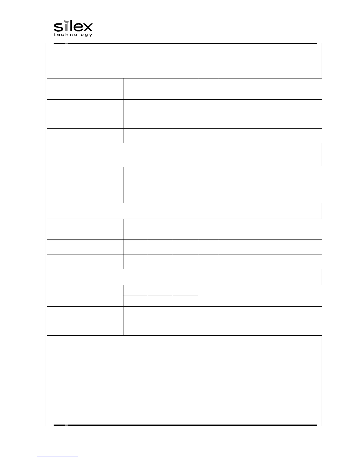
3. Board specifications
3.1. General specifications
Items
Specifications
Units
Remarks
Connection with the host board
44-pin Land Grid Array (Direct solder)
-
Antenna port
MHF1 connector x1
pc
Host interface
SDIO v3.0
-
For Wireless LAN
UART
-
For Bluetooth, up to 4Mbps
RF interface
IEEE802.11a/b/g/n/ac
-
IEEE802.11-2012
IEEE802.11ac-2013
Bluetooth 4.2 BR/EDR/LE
-
Dimensions
W x H x D
17.0 x 18.0 x 2.6
mm
3.2. Environmental conditions
Items
Specifications
Units
Remarks
Min.
Typ.
Max.
Recommended operating temperature
-20 - +85
℃
Ambient temperature
Recommended operating humidity
15 - 93
%RH
No condensing
Recommended strage temperature
-20 - +95
℃
Ambient temperature
Recommended strage humidity
10 - 95
%RH
No condensing
Page 8
Drawing No.:JW204430XX
Date:July 13, 2017
(8/27)
CONFIDENTIAL
© silex technology, Inc.
3.3. Electrical specifications
Absolute maximum rating
Items
Specifications
Units
Remarks
Min.
Typ.
Max.
Main power supply
(VDD)
-0.30
-
+3.65
V
IO power supply voltage
(VDD_GPIO_1, VDD_GPIO_2)
-0.30
-
+4.00
V
SDIO power supply voltage
(VDD_SDIO)
-0.30
-
+4.00
V
Recommended operating conditions
Main power supply/Bluetooth power supply
Items
Specifications
Units
Remarks
Min.
Typ.
Max.
Main power supply
(VDD)
+3.135
+3.30
+3.465
V
IO power supply/SDIO power supply with +3.3V operation
Items
Specifications
Units
Remarks
Min.
Typ.
Max.
IO power supply voltage
(VDD_GPIO_1, VDD_GPIO_2)
+3.14
+3.30
+3.46
V
SDIO power supply voltage
(VDD_SDIO)
+3.14
+3.30
+3.46
V
IO power supply/SDIO power supply with +1.8V operation
Items
Specifications
Units
Remarks
Min.
Typ.
Max.
IO power supply voltage
(VDD_GPIO_1, VDD_GPIO_2)
+1.71
+1.80
+1.89
V
SDIO power supply voltage
(VDD_SDIO)
+1.71
+1.80
+1.89
V
※All voltage source for the analog RF power supply is internally regulated in the module, and RF performance described in this
document is not affected by any variation for external power source.
Page 9
Drawing No.:JW204430XX
Date:July 13, 2017
(9/27)
CONFIDENTIAL
© silex technology, Inc.
Digital logic signal level
1) VIO (VDD_GPIO_1, VDD_GPIO_2, VDD_SDIO) = +3.3V operation
Items
Parameters
Specifications
Units
Remarks
Output/Input
current
Min.
Typ.
Max.
VIH
Input High voltage
-
0.7 x VIO
+3.3
VIO + 0.3
V
VIL
Input Low voltage
-
-0.3
-
0.3 x VIO
V
VOH
Output High voltage
IOH = 3mA
VIO - 0.4
- - V
VOL
Output Low voltage
IOL = -11mA
-
-
0.1 x VIO
V
2) VIO (VDD_GPIO_1, VDD_GPIO_2, VDD_SDIO) = +1.8V operation
Items
Parameters
Specifications
Units
Remarks
Output/Input
current
Min.
Typ.
Max.
VIH
Input High voltage
-
0.7 x VIO
+1.8
VIO + 0.2
V
VIL
Input Low voltage
-
-0.3
-
0.3 x VIO
V
VOH
Output High voltage
IOH = 3mA
VIO - 0.4
-
VIO
V
VOL
Output Low voltage
IOL = -11mA
-
-
0.1 x VIO
V
Page 10

Drawing No.:JW204430XX
Date:July 13, 2017
(10/27)
CONFIDENTIAL
© silex technology, Inc.
3.4. Current consumption specifications
VDD (WLAN Operation)
Items
Specifications
Units
Remarks
Mode
Standards
Typ.
Max.
Current consumption
Tx
11b
280
430
mA
2.4GHz
11g
280
430
mA
11ng HT20
280
430
mA
11ng HT40
280
430
mA
Rx
All mode
70
90
mA
Current consumption
Tx
11a
480
630
mA
5GHz
11na HT20
480
630
mA
11na HT40
480
630
mA
11ac VHT80
480
630
mA
Rx
All mode
90
110
mA
Page 11

Drawing No.:JW204430XX
Date:July 13, 2017
(11/27)
CONFIDENTIAL
© silex technology, Inc.
3.5. Wireless LAN general specifications
Items
Specifications
Units
Remarks
Chipset
QCA9377-3 (Qualcomm Atheros)
-
Operating frequencies
Band
Modes
Min
Max
2.4GHz
11b
2412
2462
MHz
11g/n/ac 20MHz
2412
2462
MHz
11g/n/ac 40MHz
2422
2452
MHz
5GHz
11a/n/ac 20MHz
5180
5825
MHz
11n/ac 40MHz
5190
5795
MHz
11ac 80MHz
5210
5775
MHz
Frequency steps
2.4GHz
11b/g/n
5
MHz
5GHz
11a/n/ac 20MHz
20
MHz
11n/ac 40MHz
40
MHz
11ac 80MHz
80
MHz
Data rates
11b
1,2,5.5L,5.5S,11L,11S
Mbps
11a/g
6,9,12,18,24,36,48,54
Mbps
11n
MCS 0,1,2,3,4,5,6,7
-
11ac
MCS 0,1,2,3,4,5,6,7,8,9
- Modulation types
11b
DSSS(DBPSK,DQPSK,CCK)
-
11a/g/n
OFDM(BPSK,QPSK,16QAM,64QAM)
-
11ac
OFDM(BPSK,QPSK,16QAM,64QAM,256QAM)
-
Page 12

Drawing No.:JW204430XX
Date:July 13, 2017
(12/27)
CONFIDENTIAL
© silex technology, Inc.
Operatable channel list
2.4GHz
US/CA
20MHz
Ch.1, 2, 3, 4, 5, 6, 7, 8, 9, 10, 11
40MHz
Ch.3, 4, 5, 6, 7, 8, 9
5GHz
US
20MHz
Ch.36,40,44,48,52,56,60,64,100,104,108,112,116,120,124,128,132,136,140,149,153,157,161,165
40MHz
Ch.38,46,54,62,102,110,118,126,134,151,159
80MHz
Ch.42,58,106,122,155
CA
20MHz
Ch.36,40,44,48,52,56,60,64,100,104,108,112,116,132,136,140,145,149,153,157,161,165
40MHz
Ch.38,46,54,62,102,110,134,151,159
80MHz
Ch.42,58,106,155
・Above region code relating channel list is programmed in the module by module manufacturer (Silex).
・Since programmed region code and channel list is binary data and user cannot know the structure of program, any customers
cannot change usable channels.
Operation theory
Client mode (Station)
Operation frequencies
Active/Passive
ad-hoc mode
2.4GHz band
11b/g/n
2412-2462MHz
Active scan
No
W52
11a/an/ac
5180-5240MHz
Active scan
No
W53
11a/an/ac
5260-5320MHz
Passive scan
No
W56
11a/an/ac
5500-5700MHz
※IC:5600-5650MHz disable
Passive scan
No
W58
11a/an/ac
5745-5825MHz
Active scan
No
Compliance with FCC requirement 15.407(c)
Data transmission is always initiated by software, which is the passed down through the MAC, through the digital and analog
baseband, and finally to the RF chip. Several special packets are initiated by the MAC. These are the only ways the digital baseband
portion will turn on the RF transmitter, which it then turns off at the end of the packet. Therefore, the transmitter will be on only
while one of the aforementioned packets is being transmitted. In other words, this device automatically discontinue transmission in
case of either absence of information to transmit or operational failure.
Page 13

Drawing No.:JW204430XX
Date:July 13, 2017
(13/27)
CONFIDENTIAL
© silex technology, Inc.
3.6. Wireless LAN transmitter specifications
2.4GHz (+25℃)
Items
Specifications
Remarks
Modes
Channels
Target Power
Units
Transmit Power
11b
Ch.1-Ch.11
+18.0
dBm
11g
Ch.1-Ch.11
+16.5
dBm
11n 20MHz
Ch.1-Ch.11
+16.5
dBm
11n 40MHz
Ch.3-Ch.9
+16.5
dBm
5GHz (+25℃)
Items
Specifications
Remarks
Modes
Channels
Target Power
Units
Transmit Power
11a
Ch.36-Ch.48
+10.0
dBm
Ch.52-Ch.64
+10.0
dBm
Ch.100-Ch.140
+10.0
dBm
Ch.149-Ch.165
+10.0
dBm
11n/ac 20MHz
Ch.36-Ch.48
+11.0
dBm
Ch.52-Ch.64
+11.0
dBm
Ch.100-Ch.140
+11.0
dBm
Ch.149-Ch.165
+11.0
dBm
11n/ac 40MHz
Ch.38-Ch.46
+10.0
dBm
Ch.54-Ch.62
+10.0
dBm
Ch.102-Ch.134
+10.0
dBm
Ch.151-Ch.159
+10.0
dBm
11ac 80MHz
Ch.42
+9.0
dBm
Ch.58
+9.0
dBm
Ch.106-Ch.122
+9.0
dBm
Ch.155
+9.5
dBm
Page 14

Drawing No.:JW204430XX
Date:July 13, 2017
(14/27)
CONFIDENTIAL
© silex technology, Inc.
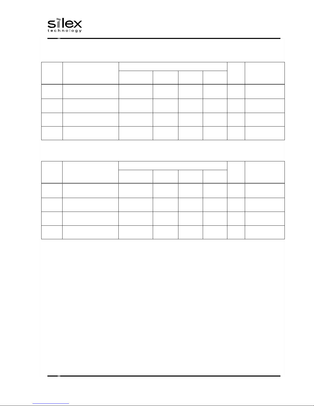
3.7. Wireless LAN Receiver specifications
2.4GHz (Operating temperature)
Items
Specifications
Remarks
Modes
Max.
Units
Receiver minimum
11b
1Mbps
-80
dBm
sensitivity
(FER<8%)
2Mbps
-80
dBm
5.5Mbps
-76
dBm
11Mbps
-76
dBm
11g
6Mbps
-82
dBm
(PER<10%)
9Mbps
-81
dBm
12Mbps
-79
dBm
18Mbps
-77
dBm
24Mbps
-74
dBm
36Mbps
-70
dBm
48Mbps
-66
dBm
54Mbps
-65
dBm
11n/ac 20MHz
MCS0
-82
dBm
HT/VHT
(PER<10%)
MCS1
-79
dBm
HT/VHT
MCS2
-77
dBm
HT/VHT
MCS3
-74
dBm
HT/VHT
MCS4
-70
dBm
HT/VHT
MCS5
-66
dBm
HT/VHT
MCS6
-65
dBm
HT/VHT
MCS7
-64
dBm
HT/VHT
MCS8
-59
dBm
VHT
11n/ac 40MHz
MCS0
-79
dBm
HT/VHT
(PER<10%)
MCS1
-76
dBm
HT/VHT
MCS2
-74
dBm
HT/VHT
MCS3
-71
dBm
HT/VHT
MCS4
-67
dBm
HT/VHT
MCS5
-63
dBm
HT/VHT
MCS6
-62
dBm
HT/VHT
MCS7
-61
dBm
HT/VHT
MCS8
-56
dBm
VHT
MCS9
-54
dBm
VHT
Page 15

Drawing No.:JW204430XX
Date:July 13, 2017
(15/27)
CONFIDENTIAL
© silex technology, Inc.
5GHz (Operating temperature)
Items
Specifications
Remarks
Modes
Max.
Units
Receiver minimum
11a
6Mbps
-82
dBm
sensitivity
(PER<10%)
9Mbps
-81
dBm
12Mbps
-79
dBm
18Mbps
-77
dBm
24Mbps
-74
dBm
36Mbps
-70
dBm
48Mbps
-66
dBm
54Mbps
-65
dBm
11n/ac 20MHz
MCS0
-82
dBm
HT/VHT
(PER<10%)
MCS1
-79
dBm
HT/VHT
MCS2
-77
dBm
HT/VHT
MCS3
-74
dBm
HT/VHT
MCS4
-70
dBm
HT/VHT
MCS5
-66
dBm
HT/VHT
MCS6
-65
dBm
HT/VHT
MCS7
-64
dBm
HT/VHT
MCS8
-59
dBm
VHT 11n/ac 40MHz
MCS0
-79
dBm
HT/VHT
(PER<10%)
MCS1
-76
dBm
HT/VHT
MCS2
-74
dBm
HT/VHT
MCS3
-71
dBm
HT/VHT
MCS4
-67
dBm
HT/VHT
MCS5
-63
dBm
HT/VHT
MCS6
-62
dBm
HT/VHT
MCS7
-61
dBm
HT/VHT
MCS8
-56
dBm
VHT
MCS9
-54
dBm
VHT
11ac 80MHz
MCS0
-76
dBm
HT/VHT
(PER<10%)
MCS1
-73
dBm
HT/VHT
MCS2
-71
dBm
HT/VHT
MCS3
-68
dBm
HT/VHT
MCS4
-64
dBm
HT/VHT
MCS5
-60
dBm
HT/VHT
MCS6
-59
dBm
HT/VHT
MCS7
-58
dBm
HT/VHT
MCS8
-53
dBm
VHT
MCS9
-51
dBm
VHT
Page 16

Drawing No.:JW204430XX
Date:July 13, 2017
(16/27)
CONFIDENTIAL
© silex technology, Inc.
3.8. Bluetooth general specifications
Items
Specifications
Units
Remarks
Chipset
QCA9377-3 (Qualcomm Atheros)
-
Core specification
Bluetooth 4.2
-
Max antenna gain
+3.25dBi@2.4GHz
Operating Frequency range
Mode
Min
Max
BR/EDR/LE
2402
2480
MHz
Frequency step
BR/EDR
1
MHz
Ch.1-Ch.79
LE 2 MHz
Ch.0-Ch.39
Modulation type
GFSK(1Mbps),Π/4 DQPSK(2Mbps),8DQPSK(3Mbps)
-
3.9. Bluetooth Transmitter specifications
Bluetooth BR/EDR/LE (+25℃)
Items
Specifications
Units
Remarks
Standards
Min.
Typ.
Max.
Maximum TX power
BR
Class 2
Ch.1-Ch.79
-3.7
+0.5
+4.0
dBm
Class 2
EDR
Class 2
Ch.1-Ch.79
-6.7
-2.5
+1.0
dBm
Class 2
LE
Ch.0-Ch.39
-4.2
+1.5
+3.5
dBm
3.10. Bluetooth Receiver specifications
Bluetooth BR/EDR/LE (Operating temperature)
Items
Specifications
Units
Remarks
Receiver minimum
Standards
Packet Types
Min.
Typ.
Max.
Sensitivity
BR (BER<0.1%)
GFSK (1Mbps)
-
-90
-70
dBm
EDR
(BER<0.01%)
Π/4 DQPSK (2Mbps)
-
-89
-70
dBm
8DQPSK (3Mbps)
-
-84
-70
dBm
LE (PER<30%)
GFSK (1Mbps)
-
-94
-70
dBm
Page 17

Drawing No.:JW204430XX
Date:July 13, 2017
(17/27)
CONFIDENTIAL
© silex technology, Inc.
4. Signal pin specifications
4.1. Pin locations
Top view
Bottom view
Pin 1 marking
Page 18

Drawing No.:JW204430XX
Date:July 13, 2017
(18/27)
CONFIDENTIAL
© silex technology, Inc.
4.2. Signal specifications
Num
Signal name
Type
I/O Domain
Descriptions
1
GND
GND
GND
Ground
2
NC
NC
NC
NC pin
3
WLAN_PWD_L
PD
VDD_GPIO_1
WLAN reset. (0=Disable, 1=Enable) Internal Pull-down.
4
VDD P P
+3.135~+3.465V
5
VDD P P
+3.135~+3.465V
6
VDD P P
+3.135~+3.465V
7
VDD P P
+3.135~+3.465V
8
VDD_GPIO_1
P
P
+1.71 ~ +3.46V
9
VDD_GPIO_2
P
P
+1.71 ~ +3.46V
10
GND
GND
GND
Ground
11
GND
GND
GND
Ground
12
SD_D3
B
VDD_SDIO
SDIO Data[3] for WLAN. Since this pin is used for Bootstrap option, you must not drive this
pin until releasing the reset signal. Internal Pull-up.
13
SD_D2
B
VDD_SDIO
SDIO Data[2] for WLAN. Since this pin is used for Bootstrap option, you must not drive this
pin until releasing the reset signal. Interal Pull-up
14
SD_D1
B
VDD_SDIO
SDIO Data[1] for WLAN. Since this pin is used for Bootstrap option, you must not drive this
pin until releasing the reset signal. Interal Pull-up
15
SD_D0
B
VDD_SDIO
SDIO Data[0] for WLAN.
16
SD_CMD
B
VDD_SDIO
SDIO command for WLAN.
17
GND
GND
GND
Ground
18
SD_CLK
DI
VDD_SDIO
SDIO Clock for WLAN.
19
GND
GND
GND
Ground
20
RESERVED
DO
VDD_SDIO
Un-used signal. Keep Open. Since this pin is used for Bootstrap option, you must not drive
this pin until releasing the reset signal. Internal Pull-up.
21
VDD_SDIO P P
+1.71 ~ +3.46V
22
GND
GND
GND
Ground
23
GND
GND
GND
Ground
24
BT_UART_RXD
DI
VDD_GPIO_1
UART RXD for BT. Since this pin is used for Bootstrap option, you must not drive this pin
until releasing the reset signal.Keep Open if BT is not used.
Interal Pull-up.
25
BT_UART_CTS
DI
VDD_GPIO_1
UART CTS for BT. Since this pin is used for Bootstrap option, you must not drive this pin
until releasing the reset signal. Keep Open if BT is not used. Interal Pull-up.
Page 19

Drawing No.:JW204430XX
Date:July 13, 2017
(19/27)
CONFIDENTIAL
© silex technology, Inc.
Num
Signal name
Type
I/O Domain
Descriptions
26
BT_UART_TXD
DO
VDD_GPIO_1
UART TXD for BT. Since this pin is used for Bootstrap option, you must not drive this pin
until releasing the reset signal. Keep Open if BT is not used. Interal Pull-up.
27
BT_UART_RTS
DO
VDD_GPIO_1
UART RTS for BT. Keep Open if BT is not used.
28
NC
NC
NC
NC pin
29
RESERVED
DI
VDD
Un-used signal. Keep Open.
30
RESERVED
OD
Open drain
Un-used signal (Debug port).. Open drain output. Recommended to connect to a test pad
and need external pull-up to IO power rail of the connected external system if the debug
function is used. Keep Open if the debug function is not used.
31
GND
GND
GND
Ground
32
VDD P P
+3.135~+3.465V
33
GND
GND
GND
Ground
34
GND
GND
GND
Ground
35
BT_WKUP_HOST
OD
Open drain
BT wake-up HOST. Active High. Keep Open if BT is not used. Need external pull-up to IO
power rail of the host system. *No testing function. Need to verify with your host board. If
you need this function please contact silex support.
36
WOW
OD
Open drain
Wake on wireless signal. Active High. Open drain output. Need external pull-up to IO power
rail of the host system.
37
RESERVED
PD
VDD
Un-used signal. Keep Open. Internal Pull-down
38
BT_I2S_SCK
PD
VDD_GPIO_1
BT PCM BCK. Bootstrap option, you must not drive this pin until releasing the reset signal.
Keep Open if Bluetooth Audio is not used. Internal Pull-down.
*No testing function. Need to verify with your I2S device or CODEC. If you need this function
please contact silex support.
39
BT_I2S_WS
B
VDD_GPIO_1
BT PCM SYNC. Keep Open if Bluetooth Audio is not used. Internal pull-down.
*No testing function. Need to verify with your I2S device or CODEC. If you need this function
please contact silex support.
40
BT_I2S_SDI
DI
VDD_GPIO_1
BT PCM IN. Keep Open if Bluetooth Audio is not used.
*No testing function. Need to verify with your I2S device or CODEC. If you need this function
please contact silex support.
41
BT_I2S_SDO
DO
VDD_GPIO_1
BT PCM OUT. Keep Open if Bluetooth Audio is not used.
*No testing function. Need to verify with your I2S device or CODEC. If you need this function
please contact silex support.
42
GND
GND
GND
Ground
43
BT_PWD_L
PD
VDD_GPIO_1
BT HW reset. (0=Disable, 1=Enable) Internal Pull-down.
44
GND
GND
GND
Ground
Num
Signal name
Type
I/O
Domain
Descriptions
EXPGND
Exposed Ground
GND
GND
Exposed Ground 72 pads
Page 20

Drawing No.:JW204430XX
Date:July 13, 2017
(20/27)
CONFIDENTIAL
© silex technology, Inc.
5. Mechanical Specifications
Top view
Page 21

Drawing No.:JW204430XX
Date:July 13, 2017
(21/27)
CONFIDENTIAL
© silex technology, Inc.
6. Indication specifications
The Label is placed on the RF shielding cas.
Country of origin
Board number
Manufacturer name
Model name
+
Warning message of W52/53 for Japan
MIC Mark and number
FCC ID
IC ID
2D Code
Format:Data Matrix
(Serial number)
Serial number
(MAC Address the last 6 digits)
Family product indication
Page 22

Drawing No.:JW204430XX
Date:July 13, 2017
(22/27)
CONFIDENTIAL
© silex technology, Inc.
7. System requirements and quick start guide
1) System requirements
Prepare the host CPU board whose spec requirements are shown below.
System pecifications
Items
Descriptions
MCU (CPU)
ARM based 1.0GHz or greater SoC from any companies.
Eg. Freescale i.MX6SX – 1200MHz
Memory size
ROM : 512MB, RAM : 1GB or greater
OS
Linux any kernel distribution
Host interface
SDIO 3.0 / UART
2) Solder down SX-SDMAC-2832 on the CPU board. See “system block diagram”.
3) Connect the Antenna to the SX-SDAMC-2832S. See “Antenna location”.
4) Install the driver which is provided by Silex to the CPU board.
Any other 3rd party’s software shall be rejected due to Subsystem ID mismatch.
5) Set wireless setting via serial console and connect to the AP.
System block diagram
SX-SDMAC-2832S
SX-SDMAC-2832S+
CPU board
Page 23

Drawing No.:JW204430XX
Date:July 13, 2017
(23/27)
CONFIDENTIAL
© silex technology, Inc.
Antenna location
Attach the PCB antenna to MHF-1 connector on the SX-SDMAC module which is mounted on the 3rd vendor’s CPU board. The
PCB antenna must be placed on the dielectric material like the plastic case and must be 20 mm or more far from the CPU board.
Page 24

Drawing No.:JW204430XX
Date:July 13, 2017
(24/27)
CONFIDENTIAL
© silex technology, Inc.
8. Notifications
FCCID :N6C-PMACS
IC :4908A-PMACS
Regulatory notice
Channel Selection
For product available in the USA/Canada market, only channel 1~11 can be operated. Selection of other channels is not possible.
Fcc Rules Part 15
FCC CAUTION
Changes or modifications not expressly approved by the party responsible for compliance could void the user’s
authority to operate the equipment.
FCC Rules, Part 15 §15.19(a)(3) / IC RSS Gen §8.4
Below sentences must be indicated on the final product which contains this module inside.
This device complies with part 15 of FCC Rules and Industry Canada’s licence-exempt RSSs. Operation is subject
to the following two conditions: (1) this device may not cause harmful interference, and (2) this device must accept any
interference received, including interference that may cause undesired operation.
Le présent appareil est conforme aux CNR d’Industrie Canada applicables aux appareils radio exempts de licence. L’exploitation
est autorisée aux deux conditions suivantes : 1) l’appareil ne doit pas produire de brouillage; 2) l’utilisateur de l’appareil doit
accepter tout brouillage radioélectrique subi, même si le brouillage est susceptible d’en compromettre le fonctionnement.
FCC Rules Part 15 Subpart C §15.247 and Subpart E / IC RSS-102 §2.6
This equipment complies with FCC/IC radiation exposure limits set forth for an uncontrolled environment and meets the FCC radio
frequency (RF) Exposure Guidelines and RSS-102 of the IC radio frequency (RF) Exposure rules. This equipment should be installed
and operated keeping the radiator at least 20cm or more away from person’s body.
Cet équipement est conforme aux limites d’exposition aux rayonnements énoncées pour un environnement non contrôlé et
respecte les règles les radioélectriques (RF) de la FCC lignes directrices d'exposition et d ’ exposition aux fréquences
radioélectriques (RF) CNR-102 de l’IC. Cet équipement doit être installé et utilisé en gardant une distance de 20 cm ou plus entre le
radiateur et le corps humain.
Page 25

Drawing No.:JW204430XX
Date:July 13, 2017
(25/27)
CONFIDENTIAL
© silex technology, Inc.
FCC Rules Part 15 Subpart E §15.407(c)
Compliance with FCC requirement 15.407(c)
Data transmission is always initiated by software, which is the passed down through the MAC, through the digital and analog
baseband, and finally to the RF chip. Several special packets are initiated by the MAC. These are the only ways the digital baseband
portion will turn on the RF transmitter, which it then turns off at the end of the packet. Therefore, the transmitter will be on only
while one of the aforementioned packets is being transmitted. In other words, this device automatically discontinue transmission in
case of either absence of information to transmit or operational failure.
FCC Rules Part 15 Subpart E §15.407(g)
Frequency Tolerance: +/-20 ppm
FCC Rules Part 15 Subpart C §15.247(g) / Subpart E
This device and its antenna(s) must not be co-located or operation in conjunction with any other antenna or transmitter.
RSS-Gen §8.3
This radio transmitter 4908A-PMACS has been approved by Industry Canada to operate with the antenna types listed below with
the maximum permissible gain and required antenna impedance for each antenna type indicated. Antenna types not included in this
list, having a gain greater than the maximum gain indicated for that type, are strictly prohibited for use with this device.
Le numéro IC du présent émetteur radio 4908A-PMACS a été approuvé par Industrie Canada pour fonctionner avec les types
d'antenne énumérés ci-dessous et ayant un gain admissible maximal et l'impédance requise pour chaque type d'antenne. Les types
d'antenne non inclus dans cette liste, ou dont le gain est supérieur au gain maximal indiqué pour ce type, sont strictement interdits
pour l'exploitation avec cet appareil.
Certified antenna list
Part number
Vendors
Antenna type
Antenna Gain
Remarks
2.4GHz
W52
W53
W56
W58
Units
146153
Molex
PCB type di-pole antenna
+3.25
+5.00
+5.00
+5.00
+5.00
dBi
Exclude cable loss
AA258 (H2B1PC1A1C)
Unictron
PCB type di-pole antenna
+2.90
+4.40
+4.40
+4.40
+4.40
dBi
Exclude cable loss
AA222 (H2B1PD1A1C)
Unictron
PCB type di-pole antenna
+2.80
+4.20
+4.20
+4.20
+4.20
dBi
Exclude cable loss
PA391-222
PFU
PCB type di-pole antenna
+3.00
+3.00
+3.00
+3.00
+3.00
dBi
Exclude cable loss
Page 26

Drawing No.:JW204430XX
Date:July 13, 2017
(26/27)
CONFIDENTIAL
© silex technology, Inc.
RSS-247 Issue 1 May 2015
Radio Standards Specification RSS-247, Issue 1, Digital Transmission Systems (DTSs), Frequency Hopping Systems (FHSs) and
Licence-Exempt Local Area Network (LE-LAN) Devices, is a new standard to replace annexes 8 and 9 of RSS-210, Issue 8,
Licence-exempt Radio Apparatus (All Frequency Bands): Category I Equipment.
At the date of publication of this standard, devices covered under the scope of this document will no longer be certified under
RSS-210, Issue 8.
Le Cahier des normes radioélectriques 247, 1re édition, Les systèmes de transmission numérique (STN), les systèmes à sauts de
fréquence (SSF) et les dispositifs de réseaux locaux exempts de licence (RL-EL), remplace les annexes 8 et 9 du CNR-210, 8e
édition, Appareils radio exempts de licence (pour toutes les bandes de fréquences) : matériel de catégorie I.
À la date de publication de la présente norme, les dispositifs visés par ce document ne seront plus certifiés conformément au
CNR-210, 8e édition.
Frequency Band 5150 – 5250 MHz
LE-LAN devices are restricted to indoor operation only in the band 5150-5250 MHz.
Les dispositifs LAN-EL sont restreints à une utilisation à l'intérieur, dans la bande 5150-5250MHz.
High-power radars are allocated as primary users (i.e. priority users) of the bands 5250-5350 MHz and 5650-5850 MHz and that
these radars could cause interference and/or damage to LE-LAN devices.
Les radars de haute puissance sont désignés comme utilisateurs principaux (c’est-à dire utilisateurs prioritaires) pour les bandes
5250-5350 MHz et 5650-5850 MHz, et que ces radars peuvent provoquer du brouillage et/ou des dommages aux dispositifs
LAN-EL.
Page 27

Drawing No.:JW204430XX
Date:July 13, 2017
(27/27)
CONFIDENTIAL
© silex technology, Inc.
WARNING:
The FCC / The Industry Canadaregulations provide that changes or modifications not expressly approved by the party responsible
for compliance could void the user’sauthority to operate the equipment.
Manual and Product Labeling information To The End User
The end user manual shall include all required regulatory information/warning as show in this manual.And when this module is
installed in the host product, you must include a “Contain FCC ID : N6C-PMACS”and a “Contain IC: 4908A-PMACS” in the label of
the host product.
This module is designed for embedded purpose into the general electric devices, and is not designed for high reliability demands
like aircraft instruments, nuclear control instruments, high reliability medical instruments, high reliability security instruments or
any other devices required extremely high reliability and quality.
• As this module communicates by radio wave, it is strongly recommended to use some security system to prevent unexpected
information leakage to others.
• This module is a radio module for embedded purpose. Please understand functions and features of this module, and evaluate as
the final product which has this module embedded. Also, as evaluation of EMC conformity of this module has not been performed,
EMC conformity evaluation and application must be performed with the final product which this module is embedded.
• This module will effect to some other device or be affected by the some other device using the same frequency band.Please
investigate the environment to use this module beforehand.
• Disassembling or modifying the radio module leads to punishment based on radio law.
• This module is the embedded module that has the exposed connectors or some devices.Please be careful for electro static,
condensing, and other dusts.
• “The OEM integrator has to be aware not to provide information to the end user regarding how to install or remove this RF module
in the user’s manual of the end product which integrates this module.”
IMPORTANT NOTE: In the event that these conditions cannot be met (for example co-location with another transmitter), then the
FCC / IC authorization is no longer considered valid and the FCC / IC ID cannot be used on the final product. In these
circumstances, the OEM integrator will be responsible for reevaluating the end product (including the transmitter) and obtaining a
separate FCC / IC authorization. As long as a condition above is met, further transmitter test will not be required. However, the
OEM integrator is still responsible for testing their end product for any additional compliance requirements required with this
module installed (for example, digital device emissions, PC peripheral requirements, etc.
 Loading...