

Page 1
(1/58)
CONFIDENTIAL
© silex technology, Inc.
Title:
IEEE802.11ac wave2
SDIO wireless LAN module
SX-SDMAC2-2830
Drawing Type :
製品仕様書
Product specifications
Drawing No.:
JW205100XX
Date :
May 30, 2019
Page 2
Drawing No.:JW205100XX
Date:May 30, 2019
(2/58)
CONFIDENTIAL
© silex technology, Inc.
改版履歴 (Revision history)
Rev.
Description
Date
Prepared by
Checked by
Approved by
XX
初版 The first edtion
May. 30, 19
Y.Kuroda
K.Hamada
Y.Shibuya
Page 3
Drawing No.:JW205100XX
Date:May 30, 2019
(3/58)
CONFIDENTIAL
© silex technology, Inc.
目次 (Index)
1. 製品概要 (Product introduction) ........................................................................................................... 4
2. ハードウェアブロック図 (Hardware block diagram) ................................................................................. 6
3. 基板仕様 (Board specifications) ........................................................................................................... 7
3.1. 一般仕様 (General specifications) .....................................................................................................7
3.2. 環境条件 (Environmental conditions) ................................................................................................8
3.3. 電気的仕様 (Electrical specifications) .................................................................................................9
3.4. 消費電流仕様 (Current consumption specifications) ........................................................................... 11
3.5. 無線 LAN 一般仕様 (Wireless LAN general specifications) .................................................................... 13
3.6. 無線 LAN 送信仕様 (Wireless LAN transmitter specifications) ............................................................... 15
3.7. 無線 LAN 受信仕様 (Wireless LAN Receiver specifications)................................................................... 18
3.8. Bluetooth 一般仕様 (Bluetooth general specifications) ....................................................................... 20
3.9. Bluetooth 送信仕様 (Bluetooth Transmitter specifications) .................................................................. 21
3.10. Bluetooth 受信仕様 (Bluetooth Receiver specifications) ...................................................................... 21
4. 信号仕様 (Signal pin specifications) .................................................................................................... 22
4.1. ピン配置 (Pin locations) ................................................................................................................ 22
4.2. 信号仕様 (Signal specifications) ..................................................................................................... 23
4.3. 信号定義 (Signal definitions) .......................................................................................................... 28
5. インターフェイス/タイミング仕様 (Interface / timing specifications) ........................................................ 29
5.1. WLAN SDIO AC タイミング仕様 (WLAN SDIO AC timing specifications) ................................................ 29
5.2. Bluetooth UART 仕様 (Bluetooth UART interface specifications) .......................................................... 33
5.3. Bluetooth 音声インターフェイス仕様(Bluetooth audio interface specifications) ........................................ 34
5.4. パワーON/OFF, リセットタイミング (Power on/off and reset timing) ..................................................... 35
6. 適合規格 (Standards Compliance) ...................................................................................................... 36
6.1. 規格一覧 (Standard list) ................................................................................................................ 36
6.2. 推奨アンテナリスト(Recommended Antenna List) .............................................................................. 37
6.3. Federal Communications Commission (FCC) Statement .................................................................... 38
6.4. Canada, Industry Canada (IC) ...................................................................................................... 40
7. 機械的仕様 (Mechanical Specifications) ............................................................................................... 42
8. 表示仕様 (Indication specifications) .................................................................................................... 43
9. 構成リスト (Components composition List) ......................................................................................... 44
10. 梱包仕様 (Packing specifications) ....................................................................................................... 45
11. 信頼性試験 (Reliability test) ............................................................................................................... 48
12. 使用上の注意 (Notifications) .............................................................................................................. 51
13. 付録 A 参考ランド設計 (Appendix-A Reference land design) ............................................................... 53
14. 付録 B SMT リフロー条件 (Appendix -B SMT reflow profiles) .............................................................. 54
15. 付録 C 仕向け毎の送信電力 (Appendix -C TX power at each destination) .............................................. 55
15.1. Japan ......................................................................................................................................... 55
15.2. EU ............................................................................................................................................. 56
15.3. US ............................................................................................................................................. 57
Page 4
Drawing No.:JW205100XX
Date:May 30, 2019
(4/58)
CONFIDENTIAL
© silex technology, Inc.
本書は SX-SDMAC2 について説明するものです。
モデル名/ハードウェアバージョン識別番号(HVIN)は「SX-SDMAC2」です。
This document describes about SX-SDMAC2.
Model name/Hardware Version Identification Number (HVIN) of this module is “SX-SDMAC2”.
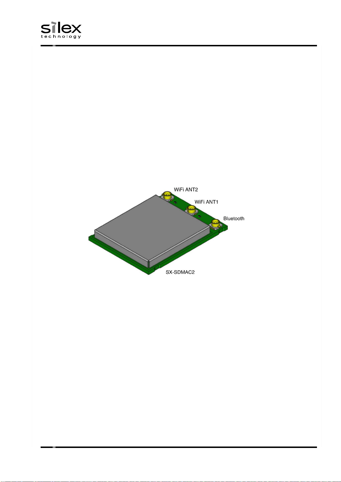
1. 製品概要 (Product introduction)
SX-SDMAC2 は、QCA9379-3 (Qualcomm Atheros 社)を採用した、2.4GHz/5GHz Dual Band IEEE 802.11
a/b/g/n/ac、Bluetooth 5.0 BR/EDR/LE (Class1) 及び SDIO3.0 準拠の無線モジュールです。本モジュールは、
MAC/BBP/RF/RF フロントエンド及び各種電源/クロックなどの外部回路を内蔵しています。
The SX-SDMAC2 is a 2.4 GHz / 5GHz dual band IEEE802.11 a/b/g/n/ac WLAN and Bluetooth 5.0
BR/EDR/LE (Class1) module based on Qualcomm QCA9379-3 chipset. The SX-SDMAC2 highly integrates
MAC, Base band, RF, RF front end and peripheral circuitry like power unit, reference clock, etc.
Page 5
Drawing No.:JW205100XX
Date:May 30, 2019
(5/58)
CONFIDENTIAL
© silex technology, Inc.
特徴 (Features)
■ IEEE802.11a/b/g/n/ac 準拠(2.4 GHz, 5 GHz)
IEEE802.11a/b/g/n/ac compliant (2.4 GHz, 5 GHz)
■ 2 スペーシャルデータストリームシステム (2T2R)
2 spatial data stream system (2T2R)
■ 5 GHz:20/40/80 MHz 帯域幅モード対応 (PHY データレート 867 Mbps)
2.4 GHz:20/40 MHz 帯域幅モード対応 (PHY データレート 300Mbps,拡張 PHY データレート 400Mbps)
5 GHz: 20/40/80 MHz bandwidth mode (PHY Data rate 867 Mbps)
2.4 GHz: 20/40 MHz bandwidth mode (PHY Data rate 300 Mbps, Extra PHY Data rate 400Mbps)
PHY Data Rate
▢ 802.11b/g 1-54 Mbps
▢ 802.11a 6-54 Mbps
▢ 802.11n 1T1R MCS0-7, 2T2R MCS8-15
▢ 802.11ac MCS0-9
■ Bluetooth 5.0 BR/EDR/LE (Class1)。Bluetooth 1.x, 2.x, 3.0, 4.0, 4.1, 4.2 後方互換
Bluetooth 5.0 BR/EDR/LE (Class1). Backward-compatible to Bluetooth 1.x, 2.x, 3.0, 4.0, 4.1, 4.2
■ Wireless LAN ホストインターフェイスとして SDIO 3.0 対応
SDIO3.0 as the Wireless LAN host interface
■ Bluetooth ホストインターフェイスとして UART 対応
UART as the Bluetooth host interface
■ 主電源+3.3V, IO 電源(VDD_GPIO1, VDD_SDIO)+1.8V/+3.3V 選択
+3.3V main power supply, selectable +1.8V/+3.3V IO power supply (VDD_GPIO1, VDD_SDIO)
■ EU RoHS 指令 2011/65/EC (Lead Free)適合
EU RoHS directive 2011/65/EC (Lead Free) compliant
Page 6
Drawing No.:JW205100XX
Date:May 30, 2019
(6/58)
CONFIDENTIAL
© silex technology, Inc.
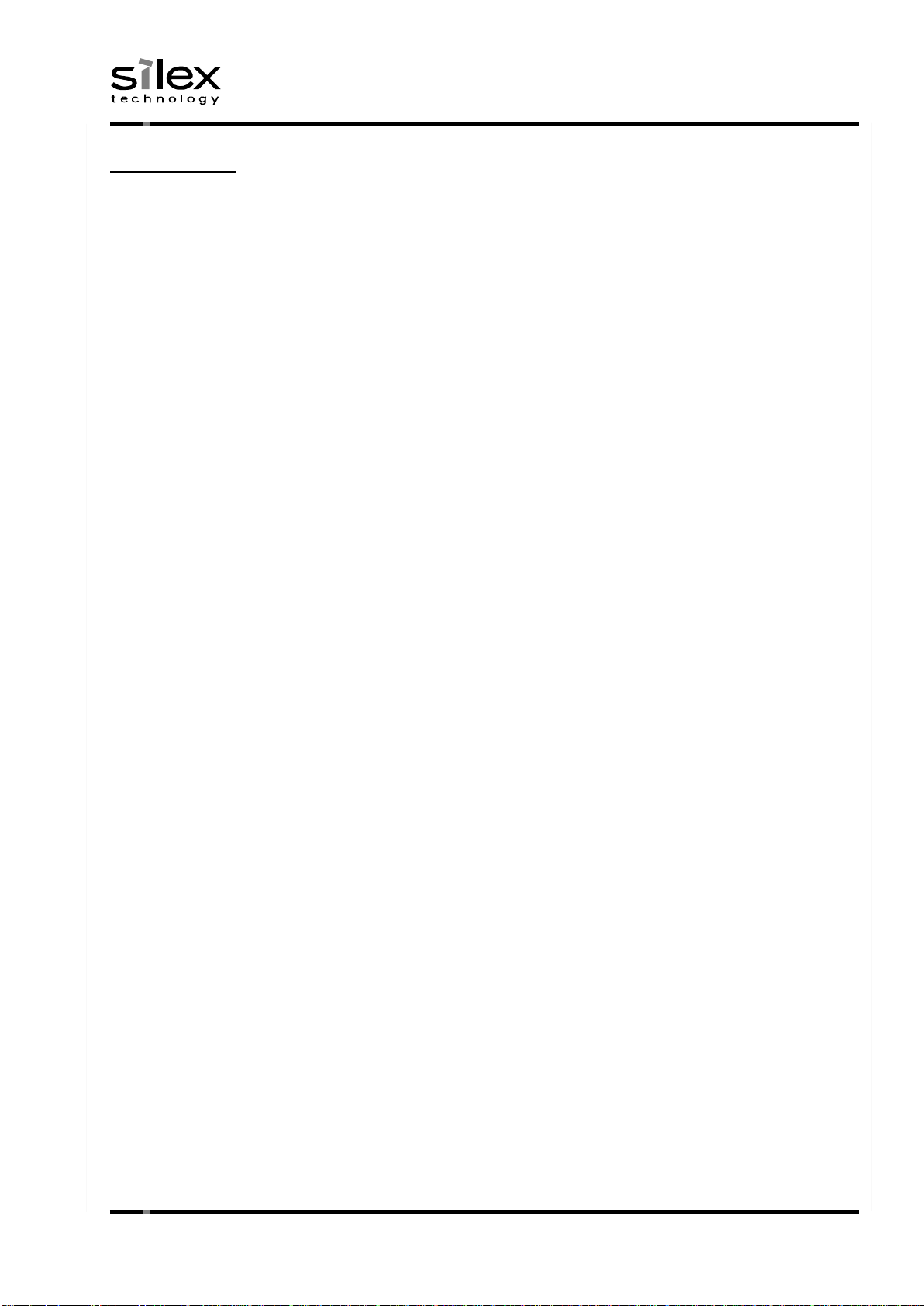
2. ハードウェアブロック図 (Hardware block diagram)
略語 (Acronyms)
PMU
Power Management Unit
DPX
Integrated Passive Device type Diplexer
MHF I
MHF-I co-axial connector (I-PEX) or compatible connector
Page 7
Drawing No.:JW205100XX
Date:May 30, 2019
(7/58)
CONFIDENTIAL
© silex technology, Inc.
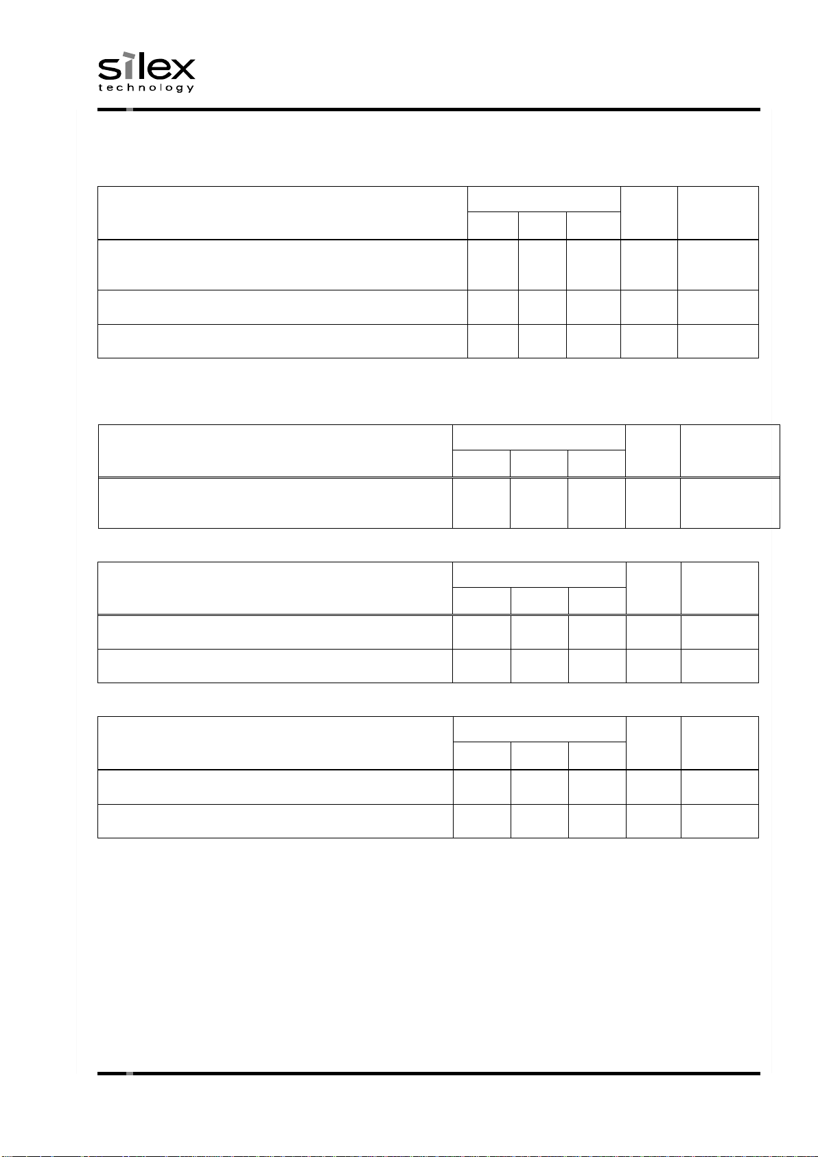
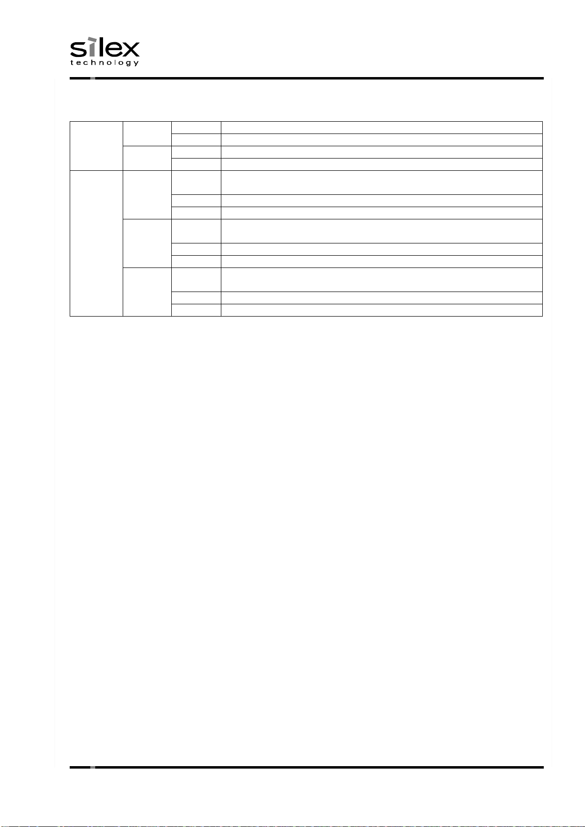
3. 基板仕様 (Board specifications)
3.1. 一般仕様 (General specifications)
Items
Specifications
Units
Remarks
ホストボードへの接続方式
Connection
with the host board
68-pin Land Grid Array
(Direct solder)
-
アンテナポート
Antenna port
MHF I connector x 3
pcs
アンテナポート特性
Antenna port characteristics
50
Ω
SWR < 3 : 1
(2.4-2.5GHz,
5.18-5.85GHz)
ホストインターフェイス
Host interface
SDIO v3.0
-
For Wireless LAN
UART
-
For Bluetooth
無線接続方式
RF interface
IEEE802.11a/b/g/n/ac
-
IEEE802.11-2012
IEEE802.11ac-2013
Bluetooth 5.0 BR/EDR/LE
-
Max antenna gain
+4.0dBi@2.4GHz
重さ
Weight
5.1 g Typ.
寸法
Dimensions
W x H x D
20.5 x 27.0 x 3.1
mm
§7 参照 (See §7)
MTTF
90,000
h
Min.
アンテナコネクタ着脱回数
Antenna connector
Desorption number of times
10
Times
Max.
リフロー回数
Reflow number of times
1
Time
Max.
ESD 耐性
ESD resistance
信号線
Signal pins
+/-2000
V
Human Body Model
JESD22-A114-F
非通電状態
(with/ no power supply)
アンテナピン
Antenna connector
+/-2000
Page 8
Drawing No.:JW205100XX
Date:May 30, 2019
(8/58)
CONFIDENTIAL
© silex technology, Inc.
3.2. 環境条件 (Environmental conditions)
Items
Specifications
Units
Remarks
Min.
Typ.
Max.
推奨動作温度
Recommended operating
temperature
-30 - +70
℃
周囲温度
Ambient temperature
実装後電源電圧印加時
After assembled with powered
推奨動作湿度
Recommended operating humidity
15 - 95
%RH
結露無きこと
No condensing
実装後電源電圧印加時
After assembled with powered
推奨保存温度 (実装後)
Recommended storage temperature
(After assembly)
-40 - +85
℃
実装後電源電圧無印加時
After assembled with no-powered
推奨保存湿度 (実装後)
Recommended storage humidity
(After assembly)
15 - 95
%RH
結露無きこと
No condensing
実装後電源電圧無印加時
After assembled with no-powered
推奨保管温度
*NOTE 1
Recommended storage temperature
(In the warehouse, before assembly)
+5 - +35
℃
梱包時。開封後は MSL に従う。
Packaged. Apply MSL after unpackaged.
推奨保管湿度
*NOTE 1
Recommended storage temperature
(In the warehouse, before assembly)
20 - 60
%RH
結露無きこと
No condensing
梱包時。開封後は MSL に従う。
Packaged. Apply MSL after unpackaged.
Moisture Sensitivity Level (MSL)
3
-
IPC/JEDEC J-STD-020D
取り扱いについては下記を参照。
See below standard for handling
IPC/JEDEC J-STD-033C
*NOTE 1
NOTE1
部品倉庫などで長期間 (弊社出荷後 1 年間)保管する際の推奨条件です。ドライパック未開封状態の場合、
この条件下でドライパック内の湿度が 10%RH 未満に保たれます。ドライパック内の湿度が 10%RH 以上
となったかどうかの判断は、保管期間に関わらず、§10 に示す湿度表示シートでご確認ください。保管期
間 1 年以上経過後や輸送時に保管条件を超えた可能性が有った場合は、製造前に湿度表示シートの確認や
ハンダ濡れ性の確認を実施することを推奨いたします。
This is condition to keep the product in the warehouse for long term (1 year after shipping from
Silex). In case of unpacked of the dry pack, humidity of inside shall be keep less than 10%RH.
To know whether humidity in the dry pack is exceed 10%RH or not, please check out the
humidity indication card (HIC). After 1 year from shipping or in case it might be exceeded this
condition due to transportation, checking HIC or checking solderability before production is
strongly recommended.
NOTE2
推奨ベーキング条件 (Recommended baking conditions)
基板単独 (Board only):125℃+10/-0℃ 24 hours
リール状態 (With reel):40℃+5/-0℃ ≦5%RH 13 days
ドライパック開封後 JEDEC J-STD-033 の取扱い条件下で≦30℃/60%RH でのフロアタイムが 168 時間
を超えた場合ベーキングが必要です。ドライパック未開封時でも、§10 に示す湿度表示シートが 10%RH
以上の色に変色している場合ベーキングが必要です。
In case ≦30℃/60%RH with handling rule of JEDEC-STD-033 and floor time is exceeded 168hrs,
baking must be necessary. Even before unpacking the dry pack, baking must be necessary if
color of HIC is changed to color of 10%RH or more.
Page 9
Drawing No.:JW205100XX
Date:May 30, 2019
(9/58)
CONFIDENTIAL
© silex technology, Inc.
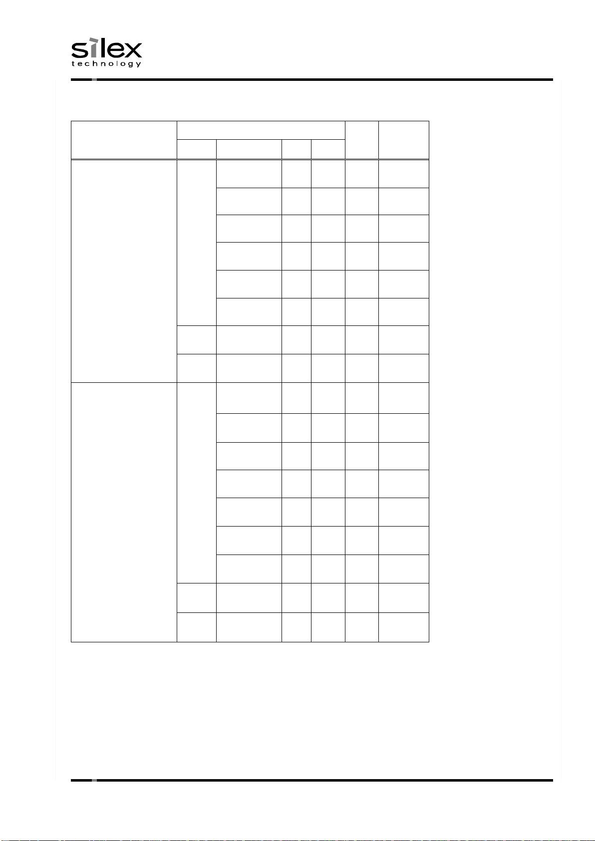
3.3. 電気的仕様 (Electrical specifications)
絶対最大定格 (Absolute maximum rating)
Items
Specifications
Units
Remarks
Min.
Typ.
Max.
主電源電圧
Main power supply
(VDD33)
-0.3
-
+3.6
V
IO 電源電圧 (VDDIO_GPIO1)
IO Power supply voltage
-0.3
-
+3.6
V
SDIO 電源電圧(VDDIO_SDIO)
SDIO Power supply voltage
-0.3
-
+3.6
V
推奨動作条件 (Recommended operating conditions)
主電源 (Main power supply)
Items
Specifications
Units
Remarks
Min.
Typ.
Max.
主電源電圧
Main power supply
(VDD33)
+3.14
+3.30
+3.46
V
IO 電源/SDIO 電源 +3.3V 動作 (IO power supply/SDIO power supply, +3.3V operation)
Items
Specifications
Units
Remarks
Min.
Typ.
Max.
IO 電源電圧 (VDDIO_GPIO1)
IO Power supply voltage
+3.14
+3.30
+3.46
V
SDIO 電源電圧(VDDIO_SDIO)
SDIO Power supply voltage
+3.14
+3.30
+3.46
V
IO 電源/SDIO 電源 +1.8V 動作 (IO power supply/SDIO power supply, +1.8V operation)
Items
Specifications
Units
Remarks
Min.
Typ.
Max.
IO 電源電圧 (VDDIO_GPIO1)
IO Power supply voltage
+1.71
+1.80
+1.89
V
SDIO 電源電圧(VDDIO_SDIO)
SDIO Power supply voltage
+1.71
+1.80
+1.89
V
Page 10
Drawing No.:JW205100XX
Date:May 30, 2019
(10/58)
CONFIDENTIAL
© silex technology, Inc.
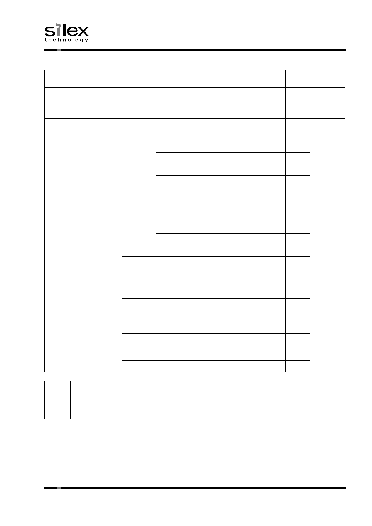
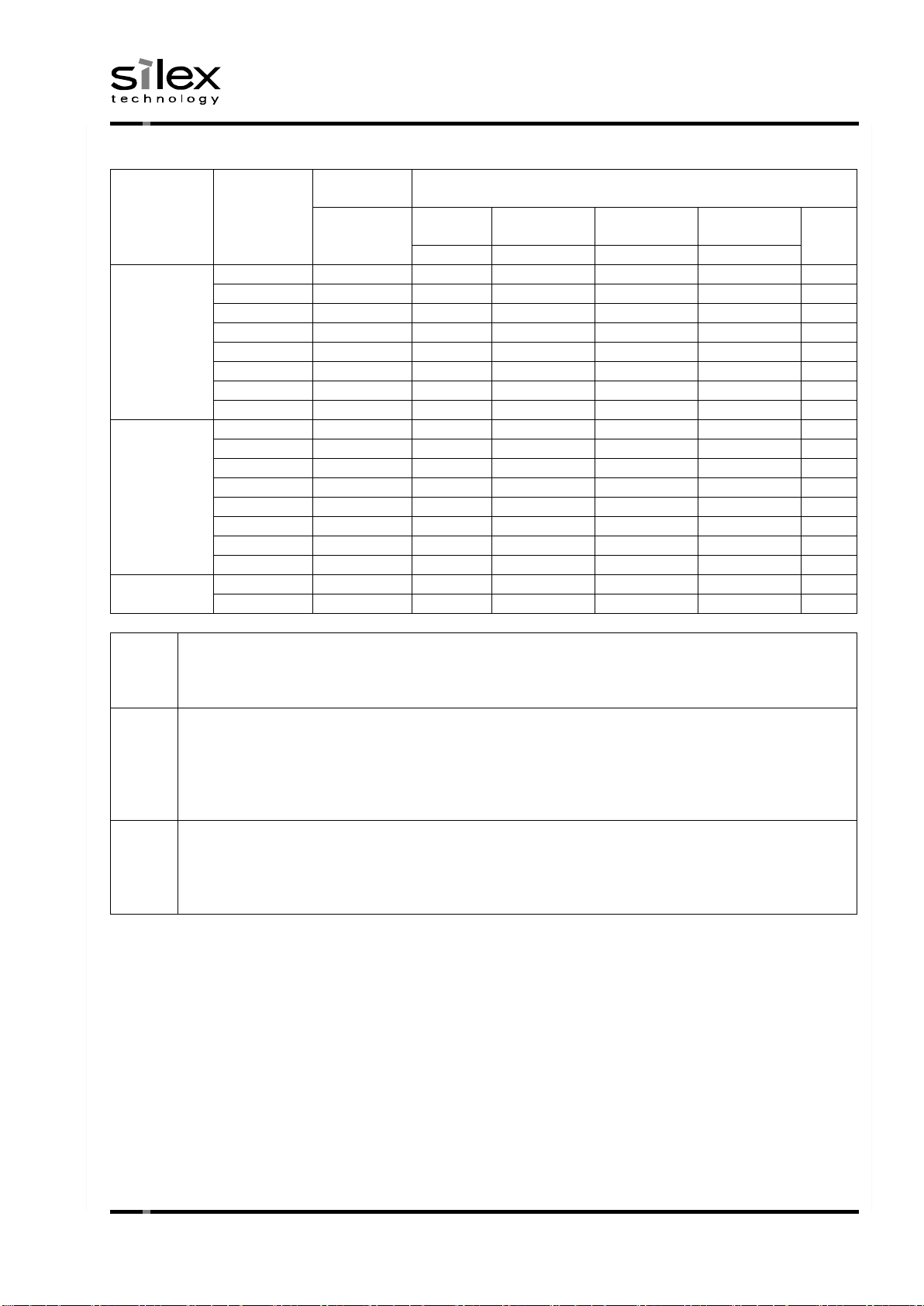
デジタル論理信号レベル (Digital logic signal level)
1) VIO (VDDIO_GPIO1, VDDIO_SDIO) = +3.3V operation
Items
Parameters
Specifications
Units
Remarks
Output/Input
current
Min.
Typ.
Max.
VIH
入力 High レベル電圧
Input High voltage
-
0.7 x VIO
+3.3
VIO +
0.3
V
VIL
入力 Low レベル電圧
Input Low voltage
-
-0.3
-
0.3 x VIO
V
VOH
出力 High レベル電圧
Output High voltage
IOH = 3mA
VIO - 0.4
-
-
V
VOL
出力 Low レベル電圧
Output Low voltage
IOL = -11mA
-
-
0.1 x VIO
V
2) VIO (VDDIO_GPIO1, VDDIO_SDIO) = +1.8V operation
Items
Parameters
Specifications
Units
Remarks
Output/Input
current
Min.
Typ.
Max.
VIH
入力 High レベル電圧
Input High voltage
-
0.7 x VIO
+1.8
VIO +
0.2
V
VIL
入力 Low レベル電圧
Input Low voltage
-
-0.3
-
0.3 x VIO
V
VOH
出力 High レベル電圧
Output High voltage
IOH = 3mA
VIO - 0.4
-
VIO
V
VOL
出力 Low レベル電圧
Output Low voltage
IOL = -11mA
-
-
0.1 x VIO
V
NOTE1
全ての I/O ピンにはシュミットトリガ回路が入っています。
シュミットヒステリシスは +1.8V IO:375mV (Typ.), +3.3V IO:645mV (Typ.)です。
Schmitt trigger is prepared for all I/O pins.
Schmitt hysteresis is +1.8V IO:375mV (Typ.), +3.3V IO:645mV (Typ.).
NOTE2
UHS-I(Ultra High Speed)モードでは VDDIO_SDIO は+1.8V のみ対応となります。
HS(High Speed)/DS(Default Speed)モードでは VDDIO_SDIO は+3.3V / +1.8V 対応となります。
Supported only VDDIO_SDIO=+1.8V as UHS-I (Ultra High Speed) mode.
Supported only VDDIO_SDIO=+1.8V/+3.3V as HS (High Speed) and DS (Default Speed) mode.
Page 11
Drawing No.:JW205100XX
Date:May 30, 2019
(11/58)
CONFIDENTIAL
© silex technology, Inc.
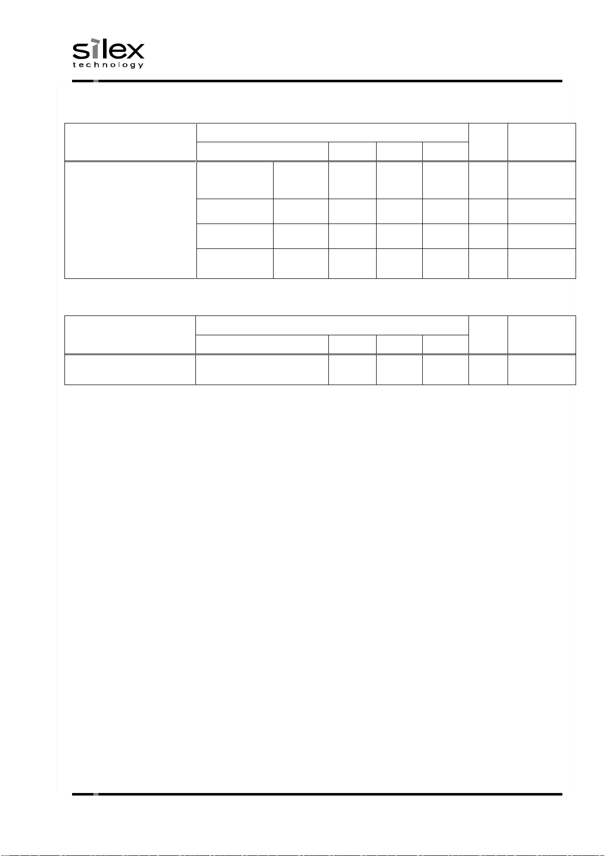
3.4. 消費電流仕様 (Current consumption specifications)
VDD (WLAN operating)
Items
Specifications
Units
Remarks
Modes
Standards
Typ.
Max.
消費電流
Current consumption
TX
11b
300
410
mA
2.4GHz
11g
330
430
mA
11ng HT20
330
400
mA
1T1R
11ng HT20
640
710
mA
2T2R
11ng HT40
330
420
mA
1T1R
11ng HT40
640
770
mA
2T2R
Rx
All mode
120
150
mA
1T1R
Rx
All mode
150
170
mA
2T2R
消費電流
Current consumption
TX
11a
490
610
mA
5GHz
11na HT20
480
580
mA
1T1R
11na HT20
920
1080
mA
2T2R
11na HT40
470
580
mA
1T1R
11na HT40
870
1040
mA
2T2R
11ac VHT80
470
580
mA
1T1R
11ac VHT80
890
1050
mA
2T2R
Rx
All mode
120
140
mA
1T1R
Rx
All mode
130
150
mA
2T2R
Page 12

Drawing No.:JW205100XX
Date:May 30, 2019
(12/58)
CONFIDENTIAL
© silex technology, Inc.
NOTE1:
Typ.: テストツールの連続送信/受信時における平均電流の個体バラつきの平均値。
Average value of unevenness of average current per unit with continuous transmit/receive
mode of the test tool.
Max.: テストツールの連続送信/受信時におけるピーク電流の個体バラつきの最大値。
Maximum value of unevenness of peak current per unit with continuous transmit/receive mode
of the test tool.
NOTE2:
総電力は VDD33(WLAN operating)と VDDIO_GPIO1 の総和になります。
モードによる組合せにご注意ください。
Total power consumption is total of VDD33 (WLAN operating) and VDDIO_GPIO1. Note that
combination of each mode.
Page 13
Drawing No.:JW205100XX
Date:May 30, 2019
(13/58)
CONFIDENTIAL
© silex technology, Inc.
3.5. 無線 LAN 一般仕様 (Wireless LAN general specifications)
Items
Specifications
Units
Remarks
チップセット
Chipset
QCA9379-3 (Qualcomm Atheros)
-
国/地域コード
Country/Region code
0x0000
-
*NOTE1
動作周波数
Band
Modes
Min
Max
Operating frequencies
2.4GHz
11b
2412
2472
MHz
11g/n/ac 20MHz
2412
2472
MHz
11g/n/ac 40MHz
2422
2462
MHz
5GHz
11a/n/ac 20MHz
5180
5825
MHz
11n/ac 40MHz
5190
5795
MHz
11ac 80MHz
5210
5775
MHz
周波数間隔
2.4GHz
11b/g/n
5
MHz
Frequency steps
5GHz
11a/n/ac 20MHz
20
MHz
11n/ac 40MHz
40
MHz
11ac 80MHz
80
MHz
データレート
11b
1,2,5.5L,5.5S,11L,11S
Mbps
Data rates
11a/g
6,9,12,18,24,36,48,54
Mbps
11n
1stream
MCS 0,1,2,3,4,5,6,7
-
11n
2stream
MCS 8,9,10,11,12,13,14,15
-
11ac
MCS 0,1,2,3,4,5,6,7,8,9
-
変調型
11b
DSSS(DBPSK,DQPSK,CCK)
-
Modulation types
11a/g/n
OFDM(BPSK,QPSK,16QAM,64QAM)
-
11ac
OFDM
(BPSK,QPSK,16QAM,64QAM,256QAM)
-
暗号化
RC4
128
bits
Encryptions
AES
128
bits
NOTE1
国/地域コードについて (Country/Region code)
モジュールにはデフォルトで国/地域コードとして 0x0000 が書かれています。
モジュールのロード時にドライバにより任意のコードに書き換えてご使用ください。
0x0000 is programed into the memory of the module as the default value. This code is assumed
to be changed to the other code by driver when the module is loaded.
Page 14
Drawing No.:JW205100XX
Date:May 30, 2019
(14/58)
CONFIDENTIAL
© silex technology, Inc.
利用可能チャネルリスト (Operatable channel list)
2.4GHz
US/CA
20MHz
Ch.1, 2, 3, 4, 5, 6, 7, 8, 9, 10, 11
40MHz
Ch.3, 4, 5, 6, 7, 8, 9
EU/JP
20MHz
Ch.1, 2, 3, 4, 5, 6, 7, 8, 9, 10, 11, 12, 13
40MHz
Ch.3, 4, 5, 6, 7, 8, 9, 10, 11
5GHz
US
20MHz
Ch.36,40,44,48,52,56,60,64,100,104,108,112,116,120,
124,128,132,136,140,149,153,157,161,165
40MHz
Ch.38,46,54,62,102,110,118,126,134,151,159
80MHz
Ch.42,58,106,122,155
CA
20MHz
Ch.36,40,44,48,52,56,60,64,100,104,108,112,116,132,
136,140,149,153,157,161,165
40MHz
Ch.38,46,54,62,102,110,134,151,159
80MHz
Ch.42,58,106,155
EU/JP
20MHz
Ch.36,40,44,48,52,56,60,64,100,104,108,112,116,120,
124,128,132,136,140
40MHz
Ch.38,46,54,62,102,110,118,126,134
80MHz
Ch.42,58,106,122
Page 15
Drawing No.:JW205100XX
Date:May 30, 2019
(15/58)
CONFIDENTIAL
© silex technology, Inc.
3.6. 無線 LAN 送信仕様 (Wireless LAN transmitter specifications)
IEEE 802.11 規格に準拠した最大送信電力値を示すものです。
ただし、各チャネルの最終的な送信電力値は、各国の電波法認証により制限を受けます。
There is maximum TX power which is compliant with IEEE 802.11 standard.
Actual TX Power value of each channel is limited by the regulatory certification of each country, however.
2.4GHz (+25℃)
Standard
Modulation
Data Rates
2.4 GHz TX Power with IEEE 802.11
EVM and Spectral Mask at +25℃
Index
802.11b/g
802.11n/ac
20 MHz
802.11n/ac
40 MHz
Units
Typical
Typical
Typical
802.11b
BPSK
1Mbps
+21.5
dBm
QPSK
2 Mbps
+21.5
dBm
CCK
5.5 Mbps
+21.5
dBm
CCK
11 Mbps
+21.5
dBm
802.11g
BPSK
6 Mbps
+21.0
dBm
BPSK
9 Mbps
+21.0
dBm
QPSK
12 Mbps
+21.0
dBm
QPSK
18 Mbps
+21.0
dBm
16 QAM
24 Mbps
+21.0
dBm
16 QAM
36 Mbps
+20.5
dBm
64 QAM
48 Mbps
+20.0
dBm
64 QAM
54 Mbps
+19.0
dBm
802.11n/ac
BPSK
MCS0
+21.0
+19.5
dBm
QPSK
MCS1
+21.0
+19.5
dBm
QPSK
MCS2
+21.0
+19.5
dBm
16 QAM
MCS3
+21.0
+19.5
dBm
16 QAM
MCS4
+21.0
+19.5
dBm
64 QAM
MCS5
+19.5
+19.5
dBm
64 QAM
MCS6
+19.0
+19.5
dBm
64 QAM
MCS7
+18.5
+18.5
dBm
802.11ac
(optional)
256 QAM
MCS8
+17.5
+17.5
dBm
256 QAM
MCS9
+17.0
dBm
Page 16
Drawing No.:JW205100XX
Date:May 30, 2019
(16/58)
CONFIDENTIAL
© silex technology, Inc.
5GHz (+25℃)
Standard
Modulation
Data Rates
5 GHZ TX Power with IEEE 802.11
EVM and Spectral Mask at +25℃
Index
802.11a
802.11n/ac
20 MHz
802.11n/ac
40 MHz
802.11n/ac
80 MHz
Units
Typical
Typical
Typical
Typical
802.11a
BPSK
6 Mbps
+19.5
dBm
BPSK
9 Mbps
+19.5
dBm
QPSK
12 Mbps
+19.5
dBm
QPSK
18 Mbps
+19.5
dBm
16 QAM
24 Mbps
+19.5
dBm
16 QAM
36 Mbps
+18.5
dBm
64 QAM
48 Mbps
+18.0
dBm
64 QAM
54 Mbps
+17.0
dBm
802.11n/ac
BPSK
MCS0
+19.0
+18.0
+18.0
dBm
QPSK
MCS1
+19.0
+18.0
+18.0
dBm
QPSK
MCS2
+19.0
+18.0
+18.0
dBm
16 QAM
MCS3
+19.0
+18.0
+18.0
dBm
16 QAM
MCS4
+19.0
+18.0
+18.0
dBm
64 QAM
MCS5
+18.0
+18.0
+18.0
dBm
64 QAM
MCS6
+17.5
+17.5
+17.0
dBm
64 QAM
MCS7
+17.0
+16.5
+16.0
dBm
802.11ac
(optional)
256 QAM
MCS8
+15.5
+15.0
+14.0
dBm
256 QAM
MCS9
+14.0
+13.0
dBm
NOTE1
送信電力は各アンテナ Chain 単独の値です。2 Data stream 時の総電力は+3.0dB されます。
Transmit power is the value from each single chain.
When the device transmits 2 streams of data, total power can be +3.0dB.
NOTE2
各チャネルの最終的な送信電力値は、認証により制限を受けます。
FCC/CE および MIC により制限された送信電力値は§15 に記載されています。
Actual TX Power value of each channel is limited by the regulatory certification.
Please refer to the product specifications §15 regarding limited TX Power by FCC/CE and
MIC.
NOTE3
ノーマルモード(非テストモード)で測定する際は Green TX などの送信電力を動的に変える機能
は無効として測定してください。
The function that changes transmit power dynamically such as Green TX must be disabled
when measure transmit power in normal mode (Non-test mode).
Page 17
Drawing No.:JW205100XX
Date:May 30, 2019
(17/58)
CONFIDENTIAL
© silex technology, Inc.
送信パワーの不確かさ (Transmit power uncertainty) 動作温度 (Operating temperature)
Items
Specifications
Units
Remarks
Modes
Min.
Typ.
Max.
周囲環境条件による
送信パワーの不確かさ
802.11a
6-54Mbps
-2.0
-
+2.0
dB
Power uncertainty due to
environmental conditions
802.11b
1-11Mbps
-2.0
-
+2.0
dB
※温度、電源条件
Temperature, Power supply
802.11g
6-54Mbps
-2.0
-
+2.0
dB
802.11n/ac
MSC0-9
-2.0
-
+2.0
dB
周波数精度 (Frequency accuracy) 動作温度 (Operating temperature)
Item
Specifications
Unit
Remark
Standards
Min.
Typ.
Max.
周波数精度
Frequency accuracy
11a/11b/11g/11n/11ac
-20
0
+20
ppm
Page 18
Drawing No.:JW205100XX
Date:May 30, 2019
(18/58)
CONFIDENTIAL
© silex technology, Inc.
3.7. 無線 LAN 受信仕様 (Wireless LAN Receiver specifications)
2.4GHz (動作温度 / Operating temperature)
Items
Specifications
Units
Remarks
Modes
Min.
Typ.
Max.
Receiver minimum
11b
1Mbps
-
-97.0
-76.0
dBm
sensitivity
(FER<8%)
2Mbps
-
-93.0
-76.0
dBm
5.5Mbps
-
-93.0
-76.0
dBm
1x1 (1SS)
11Mbps
-
-90.0
-76.0
dBm
11g
6Mbps
-
-92.0
-82.0
dBm
(PER<10%)
9Mbps
-
-90.5
-81.0
dBm
12Mbps
-
-89.5
-79.0
dBm
18Mbps
-
-87.5
-77.0
dBm
24Mbps
-
-84.0
-74.0
dBm
36Mbps
-
-81.0
-70.0
dBm
48Mbps
-
-77.0
-66.0
dBm
54Mbps
-
-75.5
-65.0
dBm
11n/ac 20MHz
MCS0
-
-91.5
-82.0
dBm
HT/VHT
(PER<10%)
MCS1
-
-89.0
-79.0
dBm
HT/VHT
MCS2
-
-87.0
-77.0
dBm
HT/VHT
MCS3
-
-84.5
-74.0
dBm
HT/VHT
MCS4
-
-81.5
-70.0
dBm
HT/VHT
MCS5
-
-77.5
-66.0
dBm
HT/VHT
MCS6
-
-76.0
-65.0
dBm
HT/VHT
MCS7
-
-74.0
-64.0
dBm
HT/VHT
MCS8
-
-70.0
-59.0
dBm
VHT
11n/ac 40MHz
MCS0
-
-89.0
-79.0
dBm
HT/VHT
(PER<10%)
MCS1
-
-87.0
-76.0
dBm
HT/VHT
MCS2
-
-84.0
-74.0
dBm
HT/VHT
MCS3
-
-81.5
-71.0
dBm
HT/VHT
MCS4
-
-78.5
-67.0
dBm
HT/VHT
MCS5
-
-74.0
-63.0
dBm
HT/VHT
MCS6
-
-73.0
-62.0
dBm
HT/VHT
MCS7
-
-71.5
-61.0
dBm
HT/VHT
MCS8
-
-67.5
-56.0
dBm
VHT
MCS9
-
-65.5
-54.0
dBm
VHT
Page 19

Drawing No.:JW205100XX
Date:May 30, 2019
(19/58)
CONFIDENTIAL
© silex technology, Inc.
5GHz (動作温度 / Operating temperature)
Items
Specifications
Units
Remarks
Modes
Min.
Typ.
Max.
Receiver minimum
11a
6Mbps
-
-89.0
-82.0
dBm
sensitivity
(PER<10%)
9Mbps
-
-88.5
-81.0
dBm
12Mbps
-
-87.0
-79.0
dBm
1x1 (1SS)
18Mbps
-
-85.0
-77.0
dBm
24Mbps
-
-81.0
-74.0
dBm
36Mbps
-
-78.5
-70.0
dBm
48Mbps
-
-74.0
-66.0
dBm
54Mbps
-
-72.5
-65.0
dBm
11n/ac 20MHz
MCS0
-
-89.0
-82.0
dBm
HT/VHT
(PER<10%)
MCS1
-
-86.5
-79.0
dBm
HT/VHT
MCS2
-
-85.0
-77.0
dBm
HT/VHT
MCS3
-
-81.5
-74.0
dBm
HT/VHT
MCS4
-
-78.5
-70.0
dBm
HT/VHT
MCS5
-
-75.0
-66.0
dBm
HT/VHT
MCS6
-
-73.0
-65.0
dBm
HT/VHT
MCS7
-
-71.5
-64.0
dBm
HT/VHT
MCS8
-
-67.0
-59.0
dBm
VHT
11n/ac 40MHz
MCS0
-
-86.5
-79.0
dBm
HT/VHT
(PER<10%)
MCS1
-
-84.5
-76.0
dBm
HT/VHT
MCS2
-
-82.0
-74.0
dBm
HT/VHT
MCS3
-
-79.0
-71.0
dBm
HT/VHT
MCS4
-
-76.0
-67.0
dBm
HT/VHT
MCS5
-
-71.5
-63.0
dBm
HT/VHT
MCS6
-
-70.0
-62.0
dBm
HT/VHT
MCS7
-
-69.0
-61.0
dBm
HT/VHT
MCS8
-
-64.5
-56.0
dBm
VHT
MCS9
-
-63.0
-54.0
dBm
VHT
11ac 80MHz
MCS0
-
-83.5
-76.0
dBm
HT/VHT
(PER<10%)
MCS1
-
-81.5
-73.0
dBm
HT/VHT
MCS2
-
-79.0
-71.0
dBm
HT/VHT
MCS3
-
-76.0
-68.0
dBm
HT/VHT
MCS4
-
-73.0
-64.0
dBm
HT/VHT
MCS5
-
-68.0
-60.0
dBm
HT/VHT
MCS6
-
-67.0
-59.0
dBm
HT/VHT
MCS7
-
-66.0
-58.0
dBm
HT/VHT
MCS8
-
-61.0
-53.0
dBm
VHT
MCS9
-
-58.5
-51.0
dBm
VHT
Page 20

Drawing No.:JW205100XX
Date:May 30, 2019
(20/58)
CONFIDENTIAL
© silex technology, Inc.
3.8. Bluetooth 一般仕様 (Bluetooth general specifications)
Items
Specifications
Units
Remarks
チップセット
Chipset
QCA9379-3 (Qualcomm Atheros)
-
コア仕様
Core specification
Bluetooth 5.0
-
動作周波数
Mode
Min
Max
Operating Frequency range
BR/EDR/LE
2402
2480
MHz
周波数間隔
BR/EDR
1
MHz
Ch.1-Ch.79
Frequency step
LE 2 MHz
Ch.0-Ch.39
変調方式
Modulation type
GFSK(1Mbps),
Π/4 DQPSK(2Mbps),8DPSK(3Mbps)
-
LE 最大 PDU サイズ
LE maximum PDU size
123
Octets
暗号化
E0
128
bits
BR/EDR
Encryption
AES
128
bits
LE
Page 21

Drawing No.:JW205100XX
Date:May 30, 2019
(21/58)
CONFIDENTIAL
© silex technology, Inc.
3.9. Bluetooth 送信仕様 (Bluetooth Transmitter specifications)
Bluetooth BR/EDR/LE (+25℃)
Items
Specifications
Units
Remarks
Standards
Min.
Typ.
Max.
最大送信電力
BR
Class 1
Ch.1-Ch.79
-3.0
+2.5
+4.5
dBm
Maximum TX power
EDR
Class 1
Ch.1-Ch.79
-6.6
-0.9
+1.0
dBm
LE
Ch.0-Ch.39
-1.6
+2.5
+6.1
dBm
送信電力ステップ
BR
Ch.1-Ch.79
2 - 8
dB
TX power step
EDR
Ch.1-Ch.79
2.5 - 8
dB
Frequency accuracy 動作温度 (Operating temperature)
Items
Specifications
Units
Remarks
Standards
Min.
Typ.
Max.
中心周波数精度
Center frequency accuracy
BR/EDR/LE
-20 - +20
ppm
3.10. Bluetooth 受信仕様 (Bluetooth Receiver specifications)
Bluetooth BR/EDR/LE (動作温度 / Operating temperature)
Items
Specifications
Units
Remarks
最小受信感度
Standards
Packet Types
Min.
Typ.
Max.
Receiver minimum
BR (BER<0.1%)
GFSK (1Mbps)
-
-95.5
-70
dBm
Sensitivity
EDR (BER<0.01%)
Π/4
DQPSK (2Mbps)
-
-99.5
-70
dBm
8DPSK (3Mbps)
-
-87.0
-70
dBm
LE (PER<30%)
GFSK (1Mbps)
-
-96.5
-70
dBm
Page 22

Drawing No.:JW205100XX
Date:May 30, 2019
(22/58)
CONFIDENTIAL
© silex technology, Inc.
4. 信号仕様 (Signal pin specifications)
4.1. ピン配置 (Pin locations)
Page 23

Drawing No.:JW205100XX
Date:May 30, 2019
(23/58)
CONFIDENTIAL
© silex technology, Inc.
4.2. 信号仕様 (Signal specifications)
Num
Signal name
Type
I/O Domain
Descriptions
1
VDDIO_SDIO
P
P
WLAN SDIO 電源。SDIO power supply for WLAN.
+1.71 ~ +3.46V
2
VDDIO_GPIO1
P
P
IO 電源。IO power supply.
+1.71 ~ +3.46V
3
VDD33 P P
主電源。Main power supply.
+3.135~+3.465V
4
GND
GND
GND
Ground
5
SDIO_D3
B
VDDIO_SDIO
WLAN 用 SDIO Data[3]信号。Bootstrap option に使用されているため、
Reset 解除まではドライブしないでください。内部 Pull-up。
SDIO Data [3] for WLAN. Since this pin is used for Bootstrap option, you must not
drive this pin until releasing the reset signal. Internal Pull-up.
6
RESERVED
DI
VDDIO_SDIO
未使用信号。未接続処理(Open)とする。Bootstrap option に使用されているため、Reset 解
除まではドライブしないください。内部 Pull-up
Un-used signal. Keep Open. Since this pin is used for Bootstrap option, you must
not drive this pin until releasing the reset signal. Internal Pull-up.
7
SDIO_CLK
DI
VDDIO_SDIO
WLAN 用 SDIO clock 信号。
SDIO Clock for WLAN.
8
SDIO_D2
B
VDDIO_SDIO
WLAN 用 SDIO Data[2]信号。Bootstrap option に使用されているため、Reset 解除までは
ドライブしないでください。内部 Pull-up。
SDIO Data [2] for WLAN. Since this pin is used for Bootstrap option, you must not
drive this pin until releasing the reset signal. Internal Pull-up
9
SDIO_D0
B
VDDIO_SDIO
WLAN 用 SDIO Data[0]信号。
SDIO Data [0] for WLAN.
10
SDIO_D1
B
VDDIO_SDIO
WLAN 用 SDIO Data[1]信号。Bootstrap option に使用されているため、Reset 解除までは
ドライブしないでください。内部 Pull-up。
SDIO Data [1] for WLAN. Since this pin is used for Bootstrap option, you must not
drive this pin until releasing the reset signal. Internal Pull-up
11
SDIO_CMD
B
VDDIO_SDIO
WLAN 用 SDIO Command 信号。
SDIO command for WLAN.
12
GND
GND
GND
Ground
13
WLAN_PWD_L
DI
VDD33
WLAN HW リセット信号。(0=Disable, 1=Enable)内部 Pull-down。
WLAN reset. (0=Disable, 1=Enable) Internal Pull-down.
14
BT_PWD_L
DI
VDD33
BT の HW リセット信号。(0=Disable, 1=Enable) 内部 Pull-down。
BT HW reset. (0=Disable, 1=Enable) Internal Pull-down.
15
RESERVED
DO
VDD33
未使用信号(デバッグポート)。オープンドレイン出力。接続する外部システムの IO 電圧へ外
部 Pull-up 及び Test pad へ接続する。デバッグ機能を使用しない場合は、未接続処理(Open)
とする。
Un-used signal (Debug port). Open drain output. Recommended to connect to a test
pad and need external pull-up to IO power rail of the connected external system if
the debug function is used. Keep Open if the debug function is not used.
Page 24

Drawing No.:JW205100XX
Date:May 30, 2019
(24/58)
CONFIDENTIAL
© silex technology, Inc.
Num
Signal name
Type
I/O Domain
Descriptions
16
GND
GND
GND
Ground
17
GND
GND
GND
Ground
18
BT_WKUP_HOST
OD
VDD33
Bluetooth wakeup the host. Active high.
19
RESERVED
DI
VDD33
未使用信号。未接続処理(Open)とする。
Un-used signal. Keep Open.
20
QoW B VDD33
Wake on wireless 信号。アクティブ High。オープンドレイン出力。要ホストシステムの IO
電源への外部 Pull-up。
Wake on wireless signal. Active High. Open drain output. Need external pull -up to
IO power rail of the host system.
21
GND
GND
GND
Ground
22
GND
GND
GND
Ground
23
GND
GND
GND
Ground
24
GND
GND
GND
Ground
25
GND
GND
GND
Ground
26
GND
GND
GND
Ground
27
GND
GND
GND
Ground
28
VDD33 P P
主電源。Main power supply.
+3.135~+3.465V
29
VDD33 P P
主電源。Main power supply.
+3.135~+3.465V
30
VDD33 P P
主電源。Main power supply.
+3.135~+3.465V
31
VDD33 P P
主電源。Main power supply.
+3.135~+3.465V
32
VDD33 P P
主電源。Main power supply.
+3.135~+3.465V
33
GND
GND
GND
Ground
34
GND
GND
GND
Ground
Page 25

Drawing No.:JW205100XX
Date:May 30, 2019
(25/58)
CONFIDENTIAL
© silex technology, Inc.
Num
Signal name
Type
I/O Domain
Descriptions
35
GND
GND
GND
Ground
36
GND
GND
GND
Ground
37
GND
GND
GND
Ground
38
GND
GND
GND
Ground
39
GND
GND
GND
Ground
40
GND
GND
GND
Ground
41
GND
GND
GND
Ground
42
GND
GND
GND
Ground
43
GND
GND
GND
Ground
44
GND
GND
GND
Ground
45
GND
GND
GND
Ground
46
GND
GND
GND
Ground
47
GND
GND
GND
Ground
48
GND
GND
GND
Ground
49
GND
GND
GND
Ground
Page 26

Drawing No.:JW205100XX
Date:May 30, 2019
(26/58)
CONFIDENTIAL
© silex technology, Inc.
Num
Signal name
Type
I/O Domain
Descriptions
50
GND
GND
GND
Ground
51
GND
GND
GND
Ground
52
VDD33 P P
主電源。Main power supply.
+3.135~+3.465V
53
RESERVED
DI
VDD33
未使用信号。未接続処理(Open)とする。
Un-used signal. Keep Open.
54
PCM_IN
DI
VDDIO_GPIO1
BT PCM IN 信号。BT Audio 未使用時は未接続処理(Open)とする。
*動作未検証機能。接続する I2S デバイスまたは CODEC との組み合わせで別途検証が必要と
なります。使用する場合はお問い合わせください。
BT PCM IN. Keep Open if BT Audio is not used.
*No testing function. Need to verify with your I2S device or CODEC. If you need this
function please contact silex support.
55
BT_UART_CTS
DI
VDDIO_GPIO1
BT 用 UART CTS 信号。Bootstrap option に使用されているため、Reset 解除まではドライ
ブしないでください。BT 未使用時は未接続処理(Open)とする。内部 Pull-up。
UART CTS for BT. Since this pin is used for Bootstrap option, you must not drive this
pin until releasing the reset signal. Keep Open if BT is not used. Internal Pull-up.
56
BT_UART_TXD
DO
VDDIO_GPIO1
BT 用 UART TXD 信号。Bootstrap option に使用されているため、Reset 解除まではドライ
ブしないでください。BT 未使用時は未接続処理(Open)とする。内部 Pull-up。
UART TXD for BT. Since this pin is used for Bootstrap option, you must not drive this
pin until releasing the reset signal. Keep Open if BT is not used. Internal Pull-up.
57
BT_UART_RXD
DI
VDDIO_GPIO1
BT 用 UART RXD 信号。Bootstrap option に使用されているため、Reset 解除まではドライ
ブしないでください。BT 未使用時は未接続処理(Open)とする。
内部 Pull-up。
UART RXD for BT. Since this pin is used for Bootstrap option, you must not drive this
pin until releasing the reset signal.Keep Open if BT is not used.
Internal Pull-up.
58
GND
GND
GND
Ground
59
3D_FRAME_SYNC
DI
VDDIO_GPIO1
Frame sync signals from TV to sync with 3D glass via Bluetooth.
60
HOST_WKUP_BT
DI
VDDIO_GPIO1
Host wakeup Bluetooth through UART. Active Low.
61
GND
GND
GND
Ground
Page 27

Drawing No.:JW205100XX
Date:May 30, 2019
(27/58)
CONFIDENTIAL
© silex technology, Inc.
Num
Signal name
Type
I/O Domain
Descriptions
62
PCM_SYNC
DI
VDDIO_GPIO1
BT PCM SYNC 信号。BT Audio 未使用時は未接続処理(Open)とする。
内部 Pull-down. *動作未検証機能。接続する I2S デバイスまたは CODEC との組み合わせで
別途検証が必要となります。使用する場合はお問い合わせください。
BT PCM SYNC. Keep Open if BT Audio is not used. Internal pull-down.
*No testing function. Need to verify with your I2S device or CODEC. If you need this
function please contact silex support.
63
PCM_OUT
DO
VDDIO_GPIO1
BT PCM OUT 信号。BT Audio 未使用時は未接続処理(Open)とする。
*動作未検証機能。接続する I2S デバイスまたは CODEC との組み合わせで別途検証が必要と
なります。使用する場合はお問い合わせください。
BT PCM OUT. Keep Open if BT Audio is not used.
*No testing function. Need to verify with your I2S device or CODEC. If you need this
function please contact silex support.
64
GND
GND
GND
Ground
65
GND
GND
GND
Ground
66
RESERVED
DO
VDDIO_GPIO1
未使用信号。未接続処理(Open)とする。
Un-used signal. Keep Open.
67
BT_UART_RTS
DO
VDDIO_GPIO1
BT 用 UART RTS 信号。BT 未使用時は未接続処理(Open)とする。
UART RTS for BT. Keep Open if BT is not used.
68
PCM_BCK
DI
VDDIO_GPIO1
BT PCM BCK 信号。Bootstrap option に使用されているため、Reset 解除まではドライブし
ないでください。BT Audio 未使用時は未接続処理(Open)とする。内部 Pull-down. *動作未
検証機能。接続する I2S デバイスまたは CODEC との組み合わせで別途検証が必要となりま
す。使用する場合はお問い合わせください。
BT PCM BCK. Bootstrap option, you must not drive this pin until releasing the reset
signal. Keep Open if BT Audio is not used. Internal Pull-down.
*No testing function. Need to verify with your I2S device or CODEC. If you need this
function please contact silex support.
EXPGND
Exposed Ground
GND
GND
Exposed Ground 6 pads
Page 28

Drawing No.:JW205100XX
Date:May 30, 2019
(28/58)
CONFIDENTIAL
© silex technology, Inc.
4.3. 信号定義 (Signal definitions)
Symbols
Descriptions
B
CMOS 双方向デジタル信号
CMOS bidirectional digital signal
DI
CMOS デジタルインプット
CMOS digital input
DO
CMOS デジタルアウトプット
CMOS digital output
OD
オープンドレインデジタルアウトプット
Open drain digital output
P
電源
Voltage supply
GND
グランド
Ground
Page 29

Drawing No.:JW205100XX
Date:May 30, 2019
(29/58)
CONFIDENTIAL
© silex technology, Inc.
5. インターフェイス/タイミング仕様 (Interface / timing specifications)
5.1. WLAN SDIO AC タイミング仕様 (WLAN SDIO AC timing specifications)
Default Speed
Symbols
Items
Specifications
Units
Remarks
Min.
Max.
fPP
Clock frequency Data Transfer Mode
0
25
MHz fOD
Clock frequency Identification Mode
100
400
kHz
Stop:0Hz
tWL
Clock low time
10 - nsec tWH
Clock high time
10 - nsec t
TLH
Clock rise time
-
10
nsec t
THL
Clock fall time
-
10
nsec t
ISU
Input setup time
5 - nsec tIH
Input hold time
5 - nsec t
ODLY
Output Delay time during Data Transfer Mode
0
14
nsec t
ODLY
Output Delay time during Identification Mode
0
50
nsec
Page 30

Drawing No.:JW205100XX
Date:May 30, 2019
(30/58)
CONFIDENTIAL
© silex technology, Inc.
High Speed
Symbols
Items
Specifications
Units
Remarks
Min.
Max.
fPP
Clock frequency Data Transfer Mode
0
50
MHz tWL
Clock low time
7 - nsec tWH
Clock high time
7 - nsec t
TLH
Clock rise time
-
3
nsec t
THL
Clock fall time
-
3
nsec t
ISU
Input setup time
6 - nsec tIH
Input hold time
2 - nsec t
ODLY
Output Delay time during Identification Mode
-
14
nsec tOH
Output Hold time
2.5
-
nsec
Page 31

Drawing No.:JW205100XX
Date:May 30, 2019
(31/58)
CONFIDENTIAL
© silex technology, Inc.
Ultra High Speed (UHS/SDR mode)
Symbols
Items
Specifications
Units
Remarks
Min.
Max.
f
CLK
Clock frequency Data Transfer Mode
0
208
MHz
tCR
Clock rise time
-
0.2*1/ f
CLK
nsec
NOTE1
tCF
Clock fall time
-
0.2*1/ f
CLK
nsec
NOTE1
tIS
Input setup time
1.4 - nsec
SDR104
tIH
Input hold time
0.8 - nsec
SDR104
tIS
Input setup time
3.0 - nsec
SDR50
tIH
Input hold time
0.8 - nsec
SDR50
t
ODLY
Output Delay time during Identification Mode
-
7.5
nsec
SDR50
t
ODLY
Output Delay time during Identification Mode
-
14
nsec
SDR25
t
OHLD
Output Hold time
1.5 - nsec tOP
Card Output phase
0
9.6
nsec
SDR104
t
ODW
Output valid data window
2.88
-
nsec
SDR104
NOTE1:
0.96 nsec(Max.) at SDR104 (208MHz)
2.00 nsec(Max.) at SDR50 (100MHz)
40.00 nsec(Max.) at SDR25 (50MHz)
Page 32

Drawing No.:JW205100XX
Date:May 30, 2019
(32/58)
CONFIDENTIAL
© silex technology, Inc.
SDIO 信号の配線について (SDIO signal length)
SDIO 信号は SD_CLK を基準に外部回路等遅延配線としてください。
Skew of SDIO signal lines are recommended on the host board.
Signals
PCB
Difference from
SD_CLK signal
Units
SD_CLK
5.6581
0
mm
SD_CMD
4.1752
-1.483
mm
SD_DATA3
6.5884
+0.9303
mm
SD_DATA2
5.4256
-0.2325
mm
SD_DATA1
4.5592
-1.0989
mm
SD_DATA0
3.727
-1.9311
mm
表内の各数値はモジュール上での各信号配線長を、Diff from CLK の数値は SD_CLK との配線長差を示しています。Diff
from CLK の値が”+”の場合は SD_CLK より短く、”-”の場合は SD_CLK より長くホストボード上で配線することで等
遅等長配線となるようにしてください。
The value of tables means the length of SDIO signals on the module, and Diff from CLK means the difference
of each SD signal’s length from SD_CLK. “+” means the length of SD signal should be shorter from SD_CLK,
“-” means the length of SD signal should be longer from SD_CLK on your board to equate the length of SD
signals.
Page 33

Drawing No.:JW205100XX
Date:May 30, 2019
(33/58)
CONFIDENTIAL
© silex technology, Inc.
5.2. Bluetooth UART 仕様 (Bluetooth UART interface specifications)
本モジュールは HCI 上位レイヤーBluetooth スタック互換の HCI-UART 規格をサポートしています。
This module supports standard HCI-UART interface so it’s compatible with HCI upper layer Bluetooth
stacks.
Items
Specification
Units
Remarks
Baud rates
115200, 375000, 460800,
750000, 1500000, 3000000, 4000000
bps
Number of data bits
8
bits Parity bit
None
-
Stop bit
1
bit Flow control
RTS/CTS
-
※フロー制御が必要です。
Flow control is necessary.
※詳しくは Bluetooth SIG の最新の Bluetooth Core 仕様書を参照してください。
See Bluetooth core specifications from Bluetooth SIG for further information.
https://www.bluetooth.com/specifications/
リンク URL は予告なく変更または削除される可能性がございます。
The Link URL might be changed or be removed without notification.
Page 34

Drawing No.:JW205100XX
Date:May 30, 2019
(34/58)
CONFIDENTIAL
© silex technology, Inc.
5.3. Bluetooth 音声インターフェイス仕様(Bluetooth audio interface specifications)
本モジュールの Bluetooth オーディオインターフェイスは、ソフトウェアによるレジスタ設定によって PCM と I2S
のプロトコルを切り替えて使用することができます。
The audio interface of this module is configurable either PCM or I2S protocol by top-level register setting
of software.
CODEC types
Items
Specifications
Remarks
Codec
CVSD, SBC
Over PCM/I2S or HCI
Synchronous audio interface (SCO profile)
Items
Specifications
Units
Remarks
インターフェイスモード
Interface modes
PCM/I2S
Master/Slave(Default)
-
ソフトウェアで切り替え
Switch by Software
サンプリング周波数
Sampling frequencies
8kHz / 16 kHz サンプリング動作
8kHz / 16 kHz Sample-based operations
-
PCM データフォーマット
PCM data formats
A-law,μ-law
8-bit,13-bit,14-bit,16-bit
-
Linear mono
8K,16K,32K,48K,96K Samples
PCM クロック周波数
PCM clock frequencies
64,96,128,192,256,384,512,768,1024,1536,
1544,2048,3072,4096
kHz
I2S クロック周波数
I2S clock frequencies
2.4
MHz
Max.
Asynchronous audio interface (A2DP profile)
Items
Specifications
Units
Remarks
モード
Mode
HCI UART
Page 35

Drawing No.:JW205100XX
Date:May 30, 2019
(35/58)
CONFIDENTIAL
© silex technology, Inc.
5.4. パワーON/OFF, リセットタイミング (Power on/off and reset timing)
Power Up Sequence
Power Down Sequence
VDDIO_GPIO1
WLAN_PWD_L
BT_PWD_L
WLAN load process
(Software)
WLAN load process
(insmod or load script)
TC
VDD33
TA
TB
TD TE
BT load process
(Software)
BT load process
(insmod or load script)
Symbols
Descriptions
Specification
Units
Min.
Max.
TA
If VDDIO_GPIO1 connected to 1.8 V
1
-
μsec
If VDDIO_GPIO1 connected to 3.3 V
0
0
μsec
TB
VDDIO_GPIO1 が 90%に達してから
WLAN/BT のリセット解除(De-assert)までの時間
Time from VDDIO_GPIO1 reaches 90%
to WLAN/BT reset release (De-assert).
10
-
μsec
TC
WLAN_PWD_L=High(De-assert)から
WLAN load process を開始するまでの時間
Time from BT_PWD_L = High(De-assert)
to WLAN load process start
0 - msec
TD
WLAN/BT のリセットが Low(Assert)になってか
VDDIO_GPIO が OFF になるまでの時間
Time from WLAN/BT reset = Low to VDDIO_GPIO = OFF.
10
-
μsec
TE
If VDDIO_GPIO1 connected to 1.8 V
0
-
μsec
If VDDIO_GPIO1 connected to 3.3 V
- - μsec
Page 36

Drawing No.:JW205100XX
Date:May 30, 2019
(36/58)
CONFIDENTIAL
© silex technology, Inc.
6. 適合規格 (Standards Compliance)
6.1. 規格一覧 (Standard list)
適合規格 (Standards conformity)
■IEEE802.11-2012 (a/b/g/n)
■ IEEE802.11ac-2013
■ Bluetooth 5.0 BR/EDR/LE (DID: D036525) *アンテナ利得 (Antenna Gain) +4.0dBi (Max.)
■ SDIO v3.0
適合法規制 (Law regulation compliance)
■ 日本電波法 (MIC)
証明規則第 2 項第 1 条 第 19 号 (Infra 親機/子機, Wi-Fi Direct, Bluetooth)
証明規則第 2 項第 1 条 第 19 号の 3 (W52 Infra 親機/子機、W53 Infra 子機)
証明規則第 2 項第 1 条 第 19 号の 3 の 2 (Infra 子機)
Article 2 paragraph 1 item (19) (Infra Master/Slave mode, Wi-Fi Direct, Bluetooth)
Article 2 paragraph 1 item (19)-3 (W52 Infra Master/Slave mode、W53 Infra Slave mode)
Article 2 paragraph 1 item (19)-3-2 (Infra Slave mode)
認証番号 (Certification number) : 007-AH0068
■ FCC Part15 (Subpart C, Subpart E)
Subpart C (2.4GHz Infra 子機, Wi-Fi Direct, Bluetooth. 2.4GHz Infra Slave mode Wi-Fi Direct, Bluetooth.)
Subpart E (W52/W58 Infra 子機, W53/W56 Infra 子機. W52/W58 Infra Slave mode, W53/W56 Infra Slave
mode.)
ID: N6C-SDMAC2
■ ISED RSS-247
Subpart C (2.4GHz Infra 子機, Wi-Fi Direct, Bluetooth. 2.4GHz Infra Slave mode Wi-Fi Direct, Bluetooth.)
Subpart E (W52/W58 Infra 子機, W53/W56 Infra 子機. W52/W58 Infra Slave mode, W53/W56 Infra Slave
mode.)
ID: 4908A-SDMAC2
■ ETSI (EN 300 328, EN 301 893)
EN 300 328 (2.4GHz Infra 子機, Wi-Fi Direct, Bluetooth. 2.4GHz Infra Slave mode Wi-Fi Direct, Bluetooth.)
EN 301 893 (W52 Infra 子機, W53/W56 Infra 子機. W52 Infra Slave mode, W53/W56 Infra Slave mode.)
■ CE RoHS Directive
対応国 (Countries)
■ Asia
・ Japan
■ North America
・ US
・ Canada
■ EU
Page 37

Drawing No.:JW205100XX
Date:May 30, 2019
(37/58)
CONFIDENTIAL
© silex technology, Inc.
6.2. 推奨アンテナリスト(Recommended Antenna List)
日本 (Japan) MIC
Antennas
Vendors
Antenna
Type
2.4GHz
Gain
5GHz
Gain
No.19
2.4GHz
No.19-2
2.484GHz
No.19-3
W52/53
No.19-3-2
W56
AA258 (H2B1PC1A1C)
(Exclude cable loss)
Unictron
PCB
+2.9dBi
+4.4dBi
✔ - ✔
✔
AA222 (H2B1PD1A1C)
(Exclude cable loss)
Unictron
PCB
+2.8dBi
+4.2dBi
✔ - ✔
✔
146153
(Exclude cable loss)
Molex
PCB
+3.25dBi
+5.0dBi
✔ - ✔
✔
1000418
(Exclude cable loss)
Ethertronics
PIFA
+2.5dBi
+3.5dBi
✔ - ✔
✔
GRF1762/GRF1802
(Exclude cable loss)
VSO
Rod
+2.0dBi
+2.0dBi
✔ - ✔
✔
GRF1763
(Exclude cable loss)
VSO
Rod
+1.5dBi
+2.1dBi
✔ - ✔
✔
ANTDC-081A0/B0
(Exclude cable loss)
Sansei-Denki
Rod
+2.0dBi
+2.0dBi
✔ - ✔
✔
ANTDP-027A0
(Exclude cable loss)
Sansei-Denki
Rod
+1.5dBi
+2.1dBi
✔ - ✔
✔
アメリカ・カナダ・ヨーロッパ (USA・Canada・Europe) FCC/IC/ETSI
Antennas
Vendors
Antenna
Type
2.4GHz
Gain
5GHz
Gain
FCC Subpart-C
(2.4GHz)
FCC Subpart-E
W52/53/56/58
ETSI
EN300329
2.4GHz
ETSI
EN300329
W52/53/56
146153
(Exclude cable loss)
Molex
PCB
+3.25dBi
+5.0dBi
✔ ✔ ✔
✔
ANTDC-081A0/B0
(Exclude cable loss)
Sansei-Denki
Rod
+2.0dBi
+2.0dBi
✔ ✔ ✔
✔
NOTE1
これらの認証は silex 推奨アンテナ、silex 製ボードデータファイルと silex 製ドライバでのみ有効です。但
し、silex の推奨アンテナを使用していたとしても最終製品の形態、または silex 製ドライバ以外を使う場
合は再認証試験が必要になる可能性があります。
The above certification is effective only with the silex recommended antennas, silex
recommended board data file and driver. However, the re-certification might be required in the
case of the final product form even if the silex recommended antennas are used or no use of
the silex driver.
NOTE2
各国の EMC 認証は最終製品形態での試験が必要です。
EMC certification of each country might be required as the final product.
NOTE3
三省電機 Rod アンテナは認可済みですが、非推奨です。VSO 互換品が推奨です。
The rod antenna of Sansei-Denki’s been certified, but not recommended.
VSO’s compatible one is recommended
Page 38

Drawing No.:JW205100XX
Date:May 30, 2019
(38/58)
CONFIDENTIAL
© silex technology, Inc.
6.3. Federal Communications Commission (FCC) Statement
This device complies with Part 15 of the FCC Rules.
Operation is subject to the following two conditions:
1) this device may not cause harmful interference and
2) this device must accept any interference received, including interference that may cause undesired operation of the
device.
15.21
You are cautioned that changes or modifications not expressly approved by the part responsible for compliance could
void the user’s authority to operate the equipment.
15.105(b)
This equipment has been tested and found to comply with the limits for a Class B digital device, pursuant to part 15 of
the FCC rules. These limits are designed to provide reasonable protection against harmful interference in a residential
installation. This equipment generates, uses and can radiate radio frequency energy and, if not installed and used in
accordance with the instructions, may cause harmful interference to radio communications. However, there is no
guarantee that interference will not occur in a particular installation. If this equipment does cause harmful interference
to radio or television reception, which can be determined by turning the equipment off and on, the user is encouraged
to try to correct the interference by one or more of the following measures:
-Reorient or relocate the receiving antenna.
-Increase the separation between the equipment and receiver.
-Connect the equipment into an outlet on a circuit different from that to which the receiver is connected.
-Consult the dealer or an experienced radio/TV technician for help.
This device complies with Part 15 of the FCC Rules. Operation is subject to the following two conditions:
1) this device may not cause harmful interference and
2) this device must accept any interference received, including interference that may cause undesired operation of the
device.
Page 39

Drawing No.:JW205100XX
Date:May 30, 2019
(39/58)
CONFIDENTIAL
© silex technology, Inc.
FCC RF Radiation Exposure Statement:
1) This Transmitter must not be co-located or operating in conjunction with any other antenna or transmitter.
2) This equipment complies with RF radiation exposure limits set forth for an uncontrolled environment. This equipment
should be installed and operated with a minimum distance of 20 cm between the radiator and your body.
Test Modes
silex technology, Inc. uses various test mode programs for test set up which operate separate from production firmware.
Host integrators should contact silex technology, Inc. for assistance with test modes needed for module/host compliance
test requirements.
Additional testing, Part 15 Subpart B disclaimer
The SX-SDMAC2 modular transmitter is only FCC authorized for the specific rule parts (i.e., FCC transmitter rules) listed
on the grant, and that the host product manufacturer is responsible for compliance to any other FCC rules that apply to
the host not covered by the modular transmitter grant of certification.
Antennas
The following external antenna type have been approved for use with the “SX-SDMAC2.”
Antenna Type
Supplier
Antenna Part No.
Freq. (MHz)
Peak Antenna Gain (dBi)
PCB
ACON
AEP8P-100000
2.4GHz 2 PCB
ACON
AEP8P-100001
2.4GHz 2 PCB
ACON
AEP8P-100003
2.4GHz 2 PCB
ACON
AEP8P-100004
2.4GHz 2 PCB
ACON
AEP8P-100005
2.4GHz 2 PCB
molex
1461530100
2.4GHz
3.25
Dipole
SANSEI
TD16081A0C0
2.4GHz 2 Dipole
SANSEI
TD16081B0C0
2.4GHz 2 Dipole
JOYMAX
IWF-145XMPXX
2.4GHz
4
Antenna Type
Supplier
Antenna Part No.
Freq. (MHz)
Peak Antenna Gain (dBi)
PCB
ACON
AEP8P-100000
5GHz 3 PCB
ACON
AEP8P-100001
5GHz 3 PCB
ACON
AEP8P-100003
5GHz 3 PCB
ACON
AEP8P-100004
5GHz 3 PCB
ACON
AEP8P-100005
5GHz 3 PCB
molex
1461530100
5GHz 5 Dipole
SANSEI
TD16081A0C0
5GHz 2 Dipole
SANSEI
TD16081B0C0
5GHz
2
Page 40

Drawing No.:JW205100XX
Date:May 30, 2019
(40/58)
CONFIDENTIAL
© silex technology, Inc.
6.4. Canada, Industry Canada (IC)
This device complies with Industry Canada licence-exempt RSS standard(s).
Operation is subject to the following two conditions:
(1) this device may not cause interference, and
(2) this device must accept any interference, including interference that may cause undesired operation of the device
Le présent appareil est conforme aux CNR d'Industrie Canada applicables aux appareils
radio exempts de licence
.L'exploitation est autorisée aux deux conditions suivantes:
(1) l'appareil ne doit pas produire de brouillage, et
(2) l'utilisateur de l'appareil doit accepter tout brouillage radioélectrique subi,
même si le brouillage est susceptible d'en compromettre le fonctionnement.
Caution: Exposure to Radio Frequency Radiation.
To comply with RSS 102 RF exposure compliance requirements, a separation distance of at least 20 cm must be
maintained between the antenna of this device and all persons.
Pour se conformer aux exigences de conformité CNR 102 RF exposition, une distance de séparation d'au moins 20 cm
doit être maintenue entre l'antenne de cet appareil et toutes les personnes.
Manual Information to the End User
The OEM integrator has to be aware not to provide information to the end user regarding how to install or remove this
RF module in the user’s manual of the end product which integrates this module.
The end user manual shall include all required regulatory information/warning as shown in this manual.
Required End Product Labeling
Any device incorporating this module must include an external, visible, permanent marking or label which states:
“Contains FCC ID : N6C-SDMAC2” and “Contains IC: 4908A-SDMAC2”
Obligation d'étiquetage du produit final:
Tout dispositif intégrant ce module doit comporter un externe, visible, marquage permanent
où une étiquette qui dit: "Contient IC: 4908A-SDMAC2”
Antennas
This radio transmitter (IC: 4908A-SDMAC2, HVIN: SX-SDMAC2) has been approved by Industry Canada to operate with
the antenna types listed below with the maximum permissible gain indicated. Antenna types not included in this list,
having a gain greater than the maximum gain indicated for that type, are strictly prohibited for use with this device.
Cet émetteur radio (IC: 4908A-SDMAC2, HVIN: SX-SDMAC2) a été approuvé par Industrie Canada pour fonctionner avec
les types d'antenne énumérés ci-dessous avec le gain maximal admissible indiqué. types d'antennes non inclus dans
cette liste , ayant un gain supérieur au gain maximum indiqué pour ce type , sont strictement interdits pour une utilisation
avec cet appareil.
Page 41

Drawing No.:JW205100XX
Date:May 30, 2019
(41/58)
CONFIDENTIAL
© silex technology, Inc.
Antenna Type
Supplier
Antenna Part No.
Freq. (MHz)
Peak Antenna Gain (dBi)
PCB
ACON
AEP8P-100000
2.4GHz 2 PCB
ACON
AEP8P-100001
2.4GHz 2 PCB
ACON
AEP8P-100003
2.4GHz 2 PCB
ACON
AEP8P-100004
2.4GHz 2 PCB
ACON
AEP8P-100005
2.4GHz 2 PCB
molex
1461530100
2.4GHz
3.25
Dipole
SANSEI
TD16081A0C0
2.4GHz 2 Dipole
SANSEI
TD16081B0C0
2.4GHz 2 Dipole
JOYMAX
IWF-145XMPXX
2.4GHz
4
Antenna Type
Supplier
Antenna Part No.
Freq. (MHz)
Peak Antenna Gain (dBi)
PCB
ACON
AEP8P-100000
5GHz 3 PCB
ACON
AEP8P-100001
5GHz 3 PCB
ACON
AEP8P-100003
5GHz 3 PCB
ACON
AEP8P-100004
5GHz 3 PCB
ACON
AEP8P-100005
5GHz 3 PCB
molex
1461530100
5GHz 5 Dipole
SANSEI
TD16081A0C0
5GHz 2 Dipole
SANSEI
TD16081B0C0
5GHz
2
Page 42

Drawing No.:JW205100XX
Date:May 30, 2019
(42/58)
CONFIDENTIAL
© silex technology, Inc.
7. 機械的仕様 (Mechanical Specifications)
厚み Thickness
Item
Thickness
Description
SMT (単体)
SMT (A simple substance)
3.1mm
PCB 厚 PCB Thickness
Item
Thickness
Description
SMT (PCB)
1.00 mm +/- 0.15 mm
特に記載が無い場合、寸法公差は±0.15 mm
All dimension tolerances are ±0.15mm, unless otherwise specified.
Page 43

Drawing No.:JW205100XX
Date:May 30, 2019
(43/58)
CONFIDENTIAL
© silex technology, Inc.
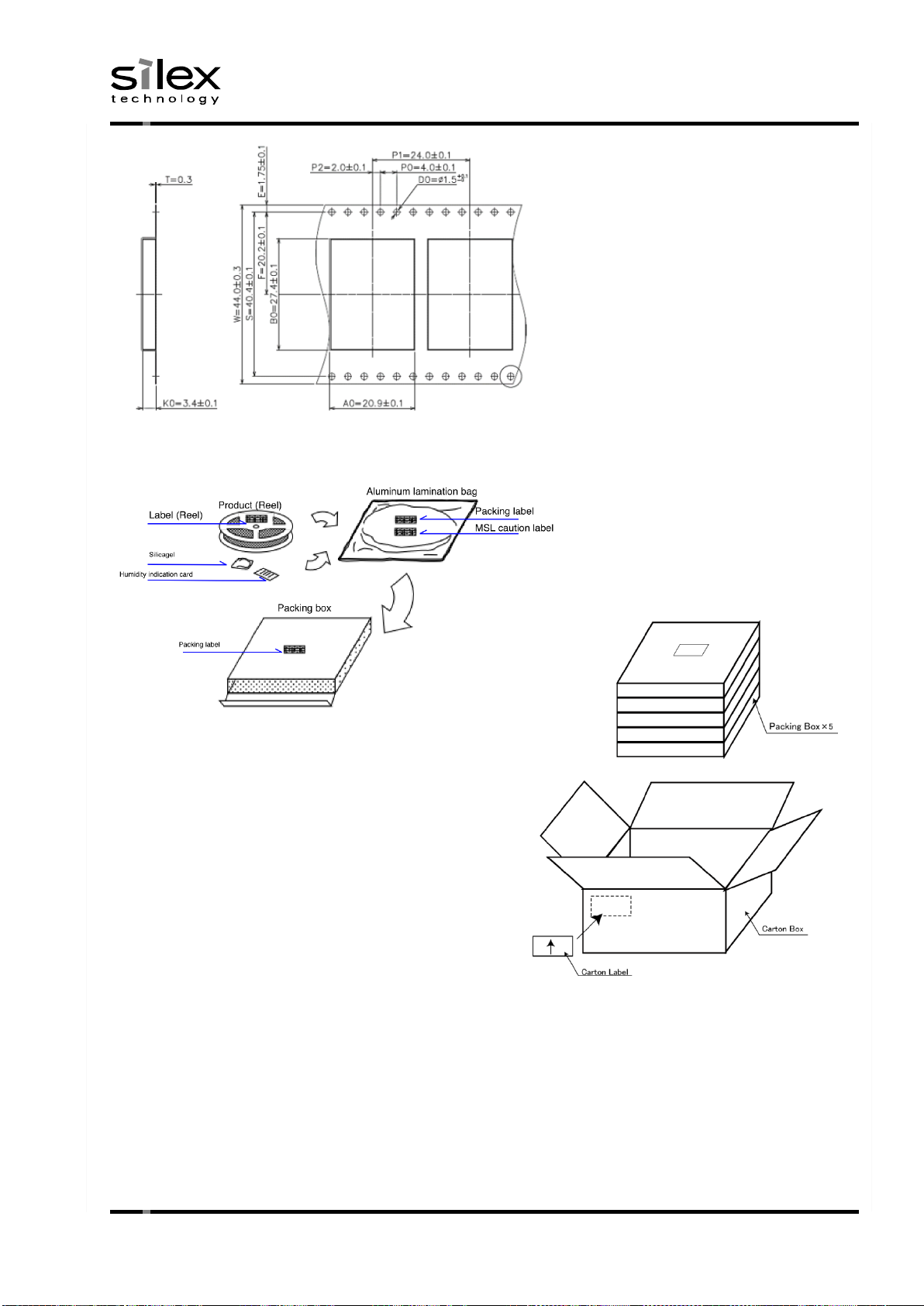
8. 表示仕様 (Indication specifications)
Page 44

Drawing No.:JW205100XX
Date:May 30, 2019
(44/58)
CONFIDENTIAL
© silex technology, Inc.
9. 構成リスト (Components composition List)
Categories
Items
Product No.
Remarks
ZXE03993
ZXE03994
SX-SDMAC2-2830
SX-SDMAC2-2830-SP
基板
Board
基板(製品)
Main Board
1 1
ラベル
EMI Label
1 1
Label
個装箱ラベル
Packing Label
1/500
1/10
MSL 警告ラベル
MSL Caution Label
1/500
1/10
集合箱ラベル
Carton Label
1/2500
1/50
付属品
Accessory
温度表示シート
Humidity Indicator
1/500
1/10
梱包
Packing
個装箱
Packing Box
1/500
1/10
集合箱
Carton Box
1/2500
1/50
アルミラミネート袋
Aluminum lamination bag
1/500
1/10
リール
Reel Set
1/500
1/10
シリカゲル
Silica gel
2/500
2/10
Page 45
Drawing No.:JW205100XX
Date:May 30, 2019
(45/58)
CONFIDENTIAL
© silex technology, Inc.
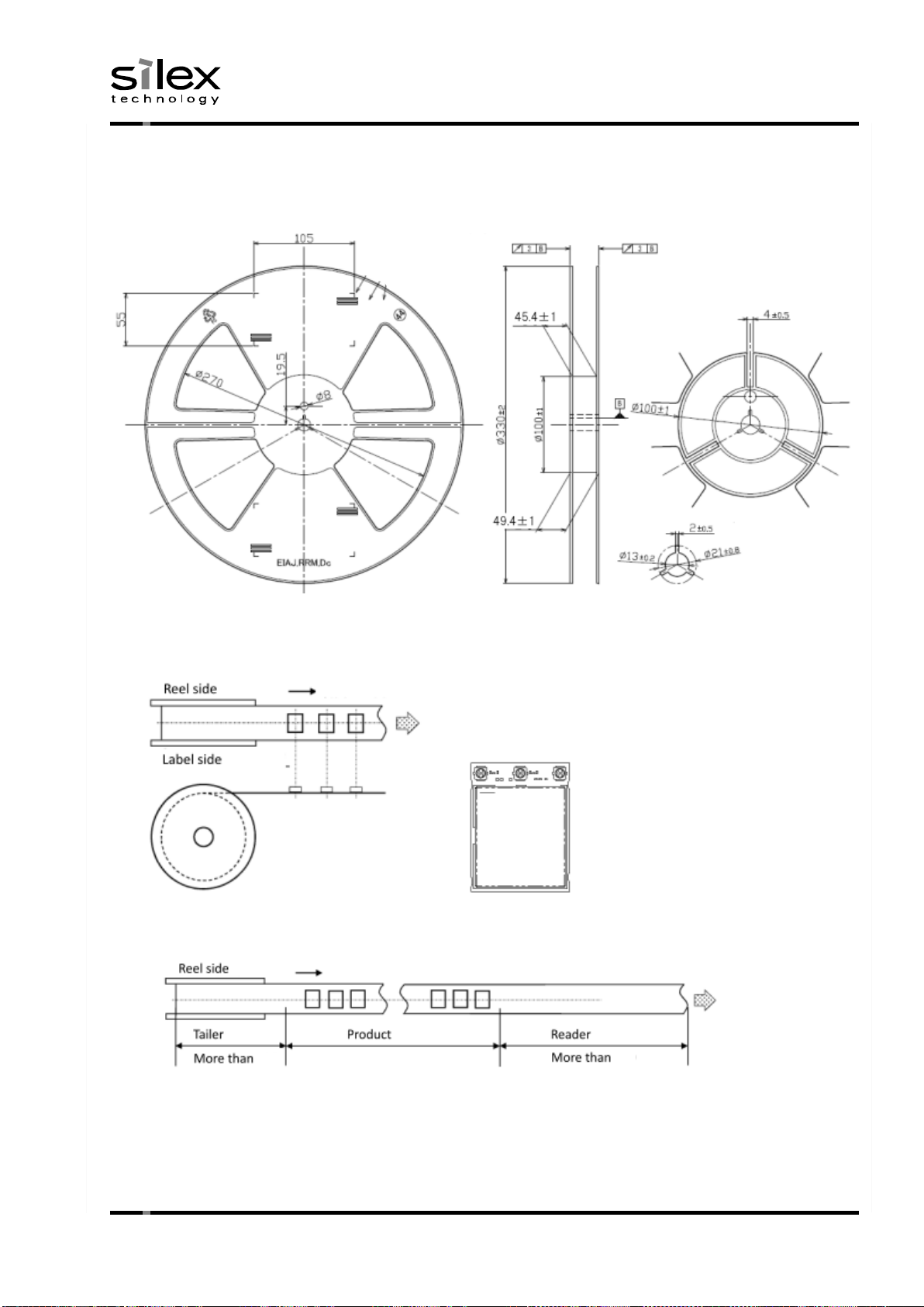
10. 梱包仕様 (Packing specifications)
(mm)
400
160
Page 46
Drawing No.:JW205100XX
Date:May 30, 2019
(46/58)
CONFIDENTIAL
© silex technology, Inc.
Page 47

Drawing No.:JW205100XX
Date:May 30, 2019
(47/58)
CONFIDENTIAL
© silex technology, Inc.
MSL 警告ラベル (MSL caution label)
(mm)
湿度表示カード例 (Example of humidity indication card)
Page 48

Drawing No.:JW205100XX
Date:May 30, 2019
(48/58)
CONFIDENTIAL
© silex technology, Inc.
11. 信頼性試験 (Reliability test)
Test items
Standards
Description
Requirements
Electricity
Appearance
DC 電圧試験
DC voltage test
-
電源電圧+3.0 V ~ +3.6 Vで動作確認を行う。
・通信の停止や通信速度の異常が起こらないことを確認する。
Check to work with +3.0 - +3.6V voltage range.
・Check no transaction stop or no throughput drop.
動作可能
Workable
NA
温湿度電圧
サイクル試験
Temperature/
Humidity cycle
test
-
下記条件で動作確認を行う。
・通信の停止や通信速度の異常が起こらないことを確認する。
Check to work with below conditions.
・Check no transaction stop or no throughput drop.
Standard test[⇨: Ramp]
(Harming)
Step 1 2 3 4 5 6 7 8 9 10 ℃ +25 ⇨ -35 ⇨ +75 ⇨ -35 ⇨ +75
+75
%RH
OFF
OFF
OFF
OFF
OFF
OFF
OFF
20
20
85
Time
0:05
1:00
2:00
1:00
2:00
1:00
4:00
1:00
2:00
6:00
Power
ON
ON
ON
ON
ON
ON
ON
ON
ON
ON
Step
11
12
- - - - - - -
-
℃ ⇨ +25
- - - - - - -
-
%RH
30
OFF
- - - - - - -
-
Time
1:00
0:10
- - - - - - -
-
Power ⇨ +25
- - - - - - -
-
Extended test[⇨: Ramp] (Harming)
Step 1 2 3 4 5 6 7 8 9 10 ℃ - ⇨ -35 ⇨ 0 ⇨ +20 ⇨ +40
+40
%RH
OFF
OFF
OFF
OFF
OFF ⇨ 10 ⇨ 10 ⇨ Time
0:00
2:00
2:00
1:00
2:00
1:00
3:00
1:00
4:00
0:45
Power
ON
ON
ON
ON
ON
ON
ON
ON
ON
ON
Step
11
12
13
14
15
16
17 - - - ℃
+40 ⇨ +75 ⇨ +40 ⇨ +25 - - - %RH
95 ⇨ 95 ⇨ 95 ⇨ 50 - - - Time
24:15
1:00
12:00
1:00
4:00
1:00
2:00 - - - Power
ON
ON
ON
ON
ON
ON
ON - -
-
動作可能
Workable
NA
高温動作試験
Functional
hot temp
-
+75℃の環境下で動作すること。
Workable at +75℃
動作可能
Workable
NA
低温動作試験
Functional
cold temp
-
-35℃の環境下で動作すること。
Workable at -35℃
動作可能
Workable
NA
Page 49

Drawing No.:JW205100XX
Date:May 30, 2019
(49/58)
CONFIDENTIAL
© silex technology, Inc.
Test items
Standards
Description
Requirements
Electricity
Appearance
衝撃試験
Mechanical
shock
test
JEDEC
JESD22-B104C
Condition B
衝撃を加えた後、動作確認を行う。
・方向と回数:X1/2 (+ /-), Y1/2 (+ /-), Z1/2 (+ /-) 各5回 (計30回)
・衝撃を加えた後も破損/故障/RF性能が劣化しないことを確認する。
Check to work after shocking.
・Axis and number of times: X1/2 (+ /-), Y1/2 (+ /-), Z1/2 (+ /-)
5 times per direction (Total 30 times)
・Damage/Defect/RF degradation is not observed after shock.
検査仕様適合
Test spec in
損傷無し
No damage
振動試験
Mechanical
vibration test
JEDEC
JESD22-B103B
Condition 1
振動を加えた後、動作確認を行う。
・方向と回数:X-Y-Z 各4分 各4回 (計12回)
・振動を加えた後も破損/故障/RF性能が劣化しないことを確認する。
Check to work after vibrating.
・Axis and number of times: X-Y-Z
4 minutes / 4 times per direction (Total 12 times)
・Damage/Defect/RF degradation is not observed after vibration.
検査仕様適合
Test spec in
損傷無し
No damage
温度衝撃試験
Thermal shock
test
JEDEC
JESD22-A106B
Test Condition C
(Fluid Air)
本製品をLxWxT=50x18x1.6mmの基板に実装後に試験を実施する。
熱衝撃を加えた後、動作確認を行う。
・Step 1 (高温) / Step 3 (低温)を繰り返す。
・100 Cycleで動作確認を実施する。
Perform after soldering this module down on the
LxWxT=50x18x1.6mm.
Check to work after heat shocking
・Repeat Step 1 (High temp.) / Step 3 (Low temp.)
・Check to work after 100 Cycles
Steps per 1 Cycle [⇨: Ramp]
Steps 1 2 3 4
Temperature
+125
+10/-0℃
⇨
-55
+0/-10℃
⇨
Time
5min
< 10sec
5min
< 10sec
Power
OFF
OFF
OFF
OFF
検査仕様適合
Test spec in
損傷無し
No damage
静電気試験
ESD test
JEDEC
JESD22-A114F
アンテナ芯線とGNDへのESD印加試験を行う。
・放電容量=100pF/放電抵抗=1.5kΩ
・アンテナコネクタ芯線:+/-2kV
・正極、負極各3回ずつの印加。
・印加した後も故障/RF性能が劣化しないことを確認する。
Add ESD to the center pin and GND ring of antenna connector.
・Discharging capacitance=100pF, Discharging resistance=1.5kΩ
・ESD level for the center pin:+/-2kV
・3 times per each plus pulse and minus pulse.
・Check no damage and no RF performance degradation after testing.
動作可能
Workable
NA
Page 50

Drawing No.:JW205100XX
Date:May 30, 2019
(50/58)
CONFIDENTIAL
© silex technology, Inc.
NOTE1
以下を除く全ての項目のサンプル数は 3 台
・温度衝撃試験:10 台
Sample numbers for all test except below is 3 units.
・Thermal shock test:10 units
Criteria
Description
損傷無し
No damage
試験後外観に損傷が無いこと。
No damage on the appearance after test.
検査仕様適合
Test spec in
RF 検査仕様を満たすこと。
Meet to RF test specifications
動作可能
Workable
試験中動作が確認できること。
Can confirm to work during test.
Page 51

Drawing No.:JW205100XX
Date:May 30, 2019
(51/58)
CONFIDENTIAL
© silex technology, Inc.
12. 使用上の注意 (Notifications)
本製品の仕様は、§6. に掲げる法規制に適合していますが、
以下の場合は仕様が変更になる可能性があります。
Specifications of this module compliant to law regulations of §6. Standards Compliance, but this shall
not apply to following cases.
1) §6.1 に掲げる国以外で使う場合。
In case this module is used in the different country from the list of §6.1
2) §6.2 に掲げるアンテナ以外を使う場合。
In case this module is used with different antenna from the antenna list of §6.2
3) 認可の更新が必要な場合。
In case the certification must be renewed.
本製品は2.4GHz 帯と 5GHz 帯の電波を媒体とする無線通信機です。法令により 5.15-5.35GHz 帯域(W52, W53)
を屋外で利用する事は禁止されております。本製品を屋外で利用される場合は予め W52 / W53 帯域の電波を出さ
ない様に設定してください。
This module is the wireless device using 2.4GHz / 5GHz band. You have to disable 5.15-5.35GHz band
(W52, W53) before use at outdoor in Japan because these band are prohibited to use at outdoor by
low restriction.
本製品は一般電子機器への組込みを目的に設計された物であり、航空機器,原子力制御,高信頼性医療器,高信頼
性セキュリティ器等、極めて高い水準の信頼性・品質を要求される機器への組込みを意図した物ではありません。
医療機器に組込む際は医療機器クラスに関係なく弊社営業までお問い合わせください。
This module is designed for embedded purpose into the general electric devices, and is not designed
for high reliability demands like aircraft instruments, nuclear control instruments, high reliability
medical instruments (Class III, IV), high reliability security instruments or any other devices required
extremely high reliability and quality. In the case embedded into the medical instrument, please
ask to silex despite the medical class.
本製品は電波を媒体として通信を行いますので、第三者への情報漏洩を防ぐ為にもセキュリティに関する設定を実
施いただく事を強く推奨します。
As this module communicates by radio wave, it is strongly recommended to use some security system
to prevent unexpected information leakage to others.
本製品は組込みを意図した無線装置です。本製品の機能、特性をご理解の上,組込み最終製品での評価をお願いい
たします。又、本無線装置単品での EMC 測定は実施しておりませんので、本無線装置を組み込んだ製品形態での
EMC 試験の実施、及び認可申請を行う必要があります。
This module is a radio module for embedded purpose. Please understand functions and features of this
module, and evaluate as the final product which has this module embedded. Also, as evaluation of
EMC conformity of this module has not been performed, EMC conformity evaluation and application
must be performed with the final product which this module is embedded.
Page 52

Drawing No.:JW205100XX
Date:May 30, 2019
(52/58)
CONFIDENTIAL
© silex technology, Inc.
本製品が使用する無線帯域において、同一周波数帯を利用する装置への影響又は装置からの影響を受ける場合があ
ります。設置においては事前に環境の調査を実施してください。
This module will effect to some other device or be affected by the some other device using the same
frequency band. Please investigate the environment to use this module beforehand.
本製品について分解や改造を行うと電波法に基づいた処罰を受ける事があります。
Disassembling or modifying the radio module leads to punishment based on radio law.
本製品は端子や部品が露出した組込み用モジュールです。製品組込み時には静電気(本製品には静電気に弱い高周
波デバイスを使用しております)や水滴,その他粉塵等には十分注意願います。
This module is the embedded module that has the exposed connectors or some devices. Please be
careful for electro static, condensing, and other dusts.
周辺で同一周波数帯を使う他の無線機器を使う場合、以下に特に注意してください。
(IEEE802.11-2012 及び IEEE802.11ac-2013 参照)
In the case using the other wireless devices using same frequency band around this product, please
take care below. (See IEEE802.11-2012 and IEEE802.11ac-2013)
1) 2.4GHz 帯では、本モジュールの中心周波数から+/- 25MHz (5Ch) 以上の間隔をあけて使用することが
推奨されます。
+/-25MHz (+/-25MHz) or more frequency separation from the center frequency of this module is
recommended in 2.4GHz.
2) 隣接チャネル及び非隣接チャネルの信号入力には十分注意して、
混信を避ける環境を設定してください。
Appropriate environment to avoid interference from the adjacent channels or the non-adjacent
channels is necessary.
▢ 2.4GHz 隣接チャネル : 中心周波数+/-25MHz(5Ch), 非隣接チャネル : 中心周波数 +/-30MHz(6Ch)以上
2.4GHz: Center frequency +/-25MHz (5Ch), Non Adjacent channel: Further than Center frequency +/-30MHz (6Ch)
▢ 5GHz HT20 隣接チャネル : 中心周波数+/-20MHz(4Ch), 非隣接チャネル : 中心周波数 +/-40MHz(8Ch)以
5GHz HT20: Center frequency +/-20MHz (4Ch), Non Adjacent channel: Further than Center frequency +/-40MHz (8Ch)
▢ 5GHz HT40 隣接チャネル : 中心周波数+/-40MHz(8Ch), 非隣接チャネル : 中心周波数 +/-80MHz(16Ch)以上
5GHz HT40 Adjacent channel: Center frequency +/-40MHz (8Ch), Non Adjacent channel: Further than Center frequency
+/-80MHz (16Ch)
▢ 5GHz HT80 隣接チャネル : 中心周波数+/-80MHz(16Ch), 非隣接チャネル : 中心周波数 +/-160MHz(32Ch)以上
5GHz HT80 Adjacent channel: Center frequency +/-80MHz (16Ch), Non Adjacent channel: Further than Center frequency
+/-160MHz (32Ch)
※上記の条件外であっても、強い電波入力が有る場合は混信する可能性が有るため、周辺の無線機器は十分距離を離し
てご使用ください。
Even if these conditions is satisfied, the module is possibly interfered when strong signal is input. The
other wireless system should be enough far from this module
対向機からの入力は、アンテナゲインを含み 2.4GHz 帯で-20dBm 以下、5GHz 帯で-30dBm 以下としてくださ
い。
The input level from the opponent device must be -20dBm or less at 2.4GHz, -30dBm or less at GHz
with including antenna gain.
Page 53

Drawing No.:JW205100XX
Date:May 30, 2019
(53/58)
CONFIDENTIAL
© silex technology, Inc.
13. 付録 A 参考ランド設計 (Appendix-A Reference land design)
(mm)
Top view
(reference stencil design)
Page 54

Drawing No.:JW205100XX
Date:May 30, 2019
(54/58)
CONFIDENTIAL
© silex technology, Inc.
14. 付録 B SMT リフロー条件 (Appendix -B SMT reflow profiles)
本推奨条件は、Sn/Ag/Cu Pb-フリーハンダを使用した場合のものです。使用するハンダの種類によって最適
化することを推奨します。
This recommended condition assumes Sn/Ag/Cu solder. This condition should be optimized per using
solder type.
Sn/Ag/Cu Pb-フリー実装 (Sn/Ag/Cu Pb-Free Assembly)
Profile Feature
Parametric
Conditions
Min.
Typ.
Max.
Units
Average ramp-up rate
TL to Tp
0 - 3.0
℃/Sec
Preheat
Temperature Ts
min
150
- - ℃
Temperature Ts
max
-
-
190
℃
Time ts
60 - 120
Sec
Time maintained above
Temperature TL
220
- - ℃
Time tL
50 - 70
Sec
Peak Temperature
Tp
240 - 245
℃
Time within 5℃ of Actual Peak Temperature
tp
-
-
20
Sec
Average ramp-down rate
-
0 - 6
℃/Sec
Time 25℃ to Peak Temperature
-
-
-
6
Min
TP
Tsmax
Tsmin
tS Preheat time
25
tP
Time 25℃ to Peak
Time
Temperature (℃)
Ramp-up
Ramp-down
TL
tL
リフロープロファイルデータ (Reflow profile data)
Page 55

Drawing No.:JW205100XX
Date:May 30, 2019
(55/58)
CONFIDENTIAL
© silex technology, Inc.
15. 付録 C 仕向け毎の送信電力 (Appendix -C TX power at each destination)
15.1. Japan
2.4GHz (+25’C)
Items
Modes
Rates
Ch.1-Ch.13
Ch.3-Ch.11
送信電力
11b
1-11Mbps
+11.5
Transmit Power
11g
6-24Mbps
+14.5
36Mbps
+14.5
Target Power (dBm)
48Mbps
+14.5
54Mbps
+14.5
11n/ac
MCS 0-2
+14.5
20MHz
MCS 3-4
+14.5
MCS 5
+14.5
MCS 6
+14.5
MCS 7
+14.5
MCS 8
+14.0
11n/ac
MCS 0-2
+14.5
40MHz
MCS 3-4
+14.5
MCS 5
+14.5
MCS 6
+14.5
MCS 7
+14.5
MCS 8
+14.0
MCS 9
+13.5
5GHz (+25’C)
Items
Modes
Rates
W52
W53
W56
送信電力
11a
6-24Mbps
+11.0
+11.0
+12.5
Transmit Power
36Mbps
+11.0
+11.0
+12.5
48Mbps
+11.0
+11.0
+12.5
Target Power (dBm)
54Mbps
+11.0
+11.0
+12.5
11n/ac
MCS 0-2
+11.5
+11.5
+13.0
20MHz
MCS 3-4
+11.5
+11.5
+13.0
MCS 5
+11.5
+11.5
+13.0
MCS 6
+11.5
+11.5
+13.0
MCS 7
+11.5
+11.5
+13.0
MCS 8
+11.5
+11.5
+12.0
11n/ac
MCS 0-2
+11.5
+11.5
+13.0
40MHz
MCS 3-4
+11.5
+11.5
+13.0
MCS 5
+11.5
+11.5
+13.0
MCS 6
+11.5
+11.5
+13.0
MCS 7
+11.5
+11.5
+13.0
MCS 8
+11.5
+11.5
+11.5
MCS 9
+10.5
+10.5
+10.5
11n/ac
MCS 0-2
+12.0
+12.0
+13.0
80MHz
MCS 3-4
+12.0
+12.0
+13.0
MCS 5
+12.0
+12.0
+13.0
MCS 6
+12.0
+12.0
+13.0
MCS 7
+12.0
+12.0
+12.5
MCS 8
+10.5
+10.5
+10.5
MCS 9
+9.5
+9.5
+9.5
Page 56

Drawing No.:JW205100XX
Date:May 30, 2019
(56/58)
CONFIDENTIAL
© silex technology, Inc.
15.2. EU
2.4GHz (+25’C)
Items
Modes
Rates
Ch.1-Ch.13
Ch.3-Ch.11
送信電力
11b
1-11Mbps
+11.0
Transmit Power
11g
6-24Mbps
+13.5
36Mbps
+13.5
Target Power (dBm)
48Mbps
+13.5
54Mbps
+13.5
11n/ac
MCS 0-2
+13.5
20MHz
MCS 3-4
+13.5
MCS 5
+13.5
MCS 6
+13.5
MCS 7
+13.5
MCS 8
+13.5
11n/ac
MCS 0-2
+13.5
40MHz
MCS 3-4
+13.5
MCS 5
+13.5
MCS 6
+13.5
MCS 7
+13.5
MCS 8
+13.5
MCS 9
+13.5
5GHz (+25’C)
Items
Modes
Rates
W52
W53
W56
W58
送信電力
11a
6-24Mbps
+11.0
+11.0
+11.0
Transmit Power
36Mbps
+11.0
+11.0
+11.0
48Mbps
+11.0
+11.0
+11.0
Target Power (dBm)
54Mbps
+11.0
+11.0
+11.0
11n/ac
MCS 0-2
+11.5
+11.5
+11.5
20MHz
MCS 3-4
+11.5
+11.5
+11.5
MCS 5
+11.5
+11.5
+11.5
MCS 6
+11.5
+11.5
+11.5
MCS 7
+11.5
+11.5
+11.5
MCS 8
+11.5
+11.5
+11.5
11n/ac
MCS 0-2
+14.0
+14.0
+13.5
40MHz
MCS 3-4
+14.0
+14.0
+13.5
MCS 5
+14.0
+14.0
+13.5
MCS 6
+14.0
+14.0
+13.5
MCS 7
+13.0
+13.0
+13.0
MCS 8
+11.5
+11.5
+11.5
MCS 9
+10.5
+10.5
+10.5
11n/ac
MCS 0-2
+13.5
+13.5
+13.0
80MHz
MCS 3-4
+13.5
+13.5
+13.0
MCS 5
+13.5
+13.5
+13.0
MCS 6
+13.5
+13.5
+13.0
MCS 7
+12.5
+12.5
+12.5
MCS 8
+10.5
+10.5
+10.5
MCS 9
+9.5
+9.5
+9.5
Page 57

Drawing No.:JW205100XX
Date:May 30, 2019
(57/58)
CONFIDENTIAL
© silex technology, Inc.
15.3. US
2.4GHz (+25’C)
Items
Modes
Rates
Ch.1
Ch.2-Ch.9
Ch.10
Ch.11
送信電力
11b
1-11Mbps
+10.0
+10.0
+10.0
+10.0
Transmit Power
11g
6-24Mbps
+15.0
+17.0
+16.5
+12.5
36Mbps
+15.0
+17.0
+16.5
+12.5
Target Power (dBm)
48Mbps
+15.0
+16.5
+16.5
+12.5
54Mbps
+15.0
+15.5
+15.5
+12.5
11n/ac
MCS 0-2
+14.5
+17.5
+17.5
+13.0
20MHz
MCS 3-4
+14.5
+17.5
+17.5
+13.0
MCS 5
+14.5
+16.0
+16.0
+13.0
MCS 6
+14.5
+15.5
+15.5
+13.0
MCS 7
+14.5
+15.0
+15.0
+13.0
MCS 8
+14.0
+14.0
+14.0
+13.0
Modes
Rates
Ch.3
Ch.4-Ch.7
Ch.8
Ch.9
11n/ac
MCS 0-2
+11.5
+12.5
+11.5
+9.5
40MHz
MCS 3-4
+11.5
+12.5
+11.5
+9.5
MCS 5
+11.5
+12.5
+11.5
+9.5
MCS 6
+11.5
+12.5
+11.5
+9.5
MCS 7
+11.5
+12.5
+11.5
+9.5
MCS 8
+11.5
+12.5
+11.5
+9.5
MCS 9
+11.5
+12.5
+11.5
+9.5
5GHz (+25’C) W52, W53
Items
Modes
Rates
Ch.36-Ch.48
Ch.52-Ch.60
Ch.64
送信電力
11a
6-24Mbps
+10.5
+15.0
+14.0
Transmit Power
36Mbps
+10.5
+15.0
+14.0
48Mbps
+10.5
+14.5
+14.0
Target Power (dBm)
54Mbps
+10.5
+13.5
+13.5
11n/ac
MCS 0-2
+10.5
+15.0
+14.0
20MHz
MCS 3-4
+10.5
+15.0
+14.0
MCS 5
+10.5
+14.5
+14.0
MCS 6
+10.5
+14.0
+14.0
MCS 7
+10.5
+13.5
+13.5
MCS 8
+10.5
+12.0
+12.0
Modes
Rates
Ch.38-Ch.46
Ch.54
Ch.62
11n/ac
MCS 0-2
+11.0
+14.0
+13.0
40MHz
MCS 3-4
+11.0
+14.0
+13.0
MCS 5
+11.0
+14.0
+13.0
MCS 6
+11.0
+14.0
+13.0
MCS 7
+11.0
+13.0
+13.0
MCS 8
+11.0
+11.5
+11.5
MCS 9
+10.5
+10.5
+10.5
Modes
Rates
Ch.42
Ch.58
11n/ac
MCS 0-2
+6.5
+11.0
80MHz
MCS 3-4
+6.5
+11.0
MCS 5
+6.5
+11.0
MCS 6
+6.5
+11.0
MCS 7
+6.5
+11.0
MCS 8
+6.5
+10.5
MCS 9
+6.5
+9.5
Page 58

Drawing No.:JW205100XX
Date:May 30, 2019
(58/58)
CONFIDENTIAL
© silex technology, Inc.
5GHz (+25’C) W56, W58
Items
Modes
Rates
Ch.100
Ch.104-Ch.136
Ch.140
Ch.149-Ch.157
Ch.165
送信電力
11a
6-24Mbps
+13.0
+15.0
+12.0
+14.5
+14.0
Transmit Power
36Mbps
+13.0
+15.0
+12.0
+14.5
+14.0
48Mbps
+13.0
+14.5
+12.0
+14.5
+14.0
Target Power (dBm)
54Mbps
+13.0
+13.5
+12.0
+13.5
+13.5
11n/ac
MCS 0-2
+13.5
+15.0
+13.5
+14.5
+14.0
20MHz
MCS 3-4
+13.5
+15.0
+13.5
+14.5
+14.0
MCS 5
+13.5
+14.5
+13.5
+14.5
+14.0
MCS 6
+13.5
+14.0
+13.5
+14.0
+14.0
MCS 7
+13.5
+13.5
+13.5
+13.5
+13.5
MCS 8
+12.0
+12.0
+12.0
+12.0
+12.0
Modes
Rates
Ch.102
Ch.110-Ch.126
Ch.134
Ch.151
Ch.159
11n/ac
MCS 0-2
+9.5
+13.5
+12.5
+11.0
+13.5
40MHz
MCS 3-4
+9.5
+13.5
+12.5
+11.0
+13.5
MCS 5
+9.5
+13.5
+12.5
+11.0
+13.5
MCS 6
+9.5
+13.5
+12.5
+11.0
+13.5
MCS 7
+9.5
+13.0
+12.5
+11.0
+13.0
MCS 8
+9.5
+11.5
+11.5
+11.0
+11.5
MCS 9
+9.5
+10.5
+10.5
+10.5
+10.5
Modes
Rates
Ch.106
Ch.122-Ch.138
Ch.155
11n/ac
MCS 0-2
+4.0
+14.5
+11.5
80MHz
MCS 3-4
+4.0
+14.5
+11.5
MCS 5
+4.0
+14.5
+11.5
MCS 6
+4.0
+13.5
+11.5
MCS 7
+4.0
+12.5
+11.5
MCS 8
+4.0
+10.5
+10.5
MCS 9
+4.0
+9.5
+9.5
NOTE1
送信電力は各アンテナ Chain 単独の値です。2 Data stream 時の総電力は+3.0dB されます。
Transmit power is the value from each single chain.
When the device transmits 2 streams of data, total power can be +3.0dB.
 Loading...