

Page 1
现货库存、技术资料、百科信息、热点资讯,精彩尽在鼎好!
5-V Low-Drop Fixed Voltage Regulator TLE 4271
Features
• Output voltage tolerance ≤ ± 2%
• Low-drop voltage
• Integrated overtemperature protection
• Reverse polarity protection
• Input voltage up to 42 V
• Overvoltage protection up to 65 V (≤ 400 ms)
• Short-circuit proof
• Suitable for use in automotive electronics
• Wide temperature range
• Adjustable reset and watchdog time
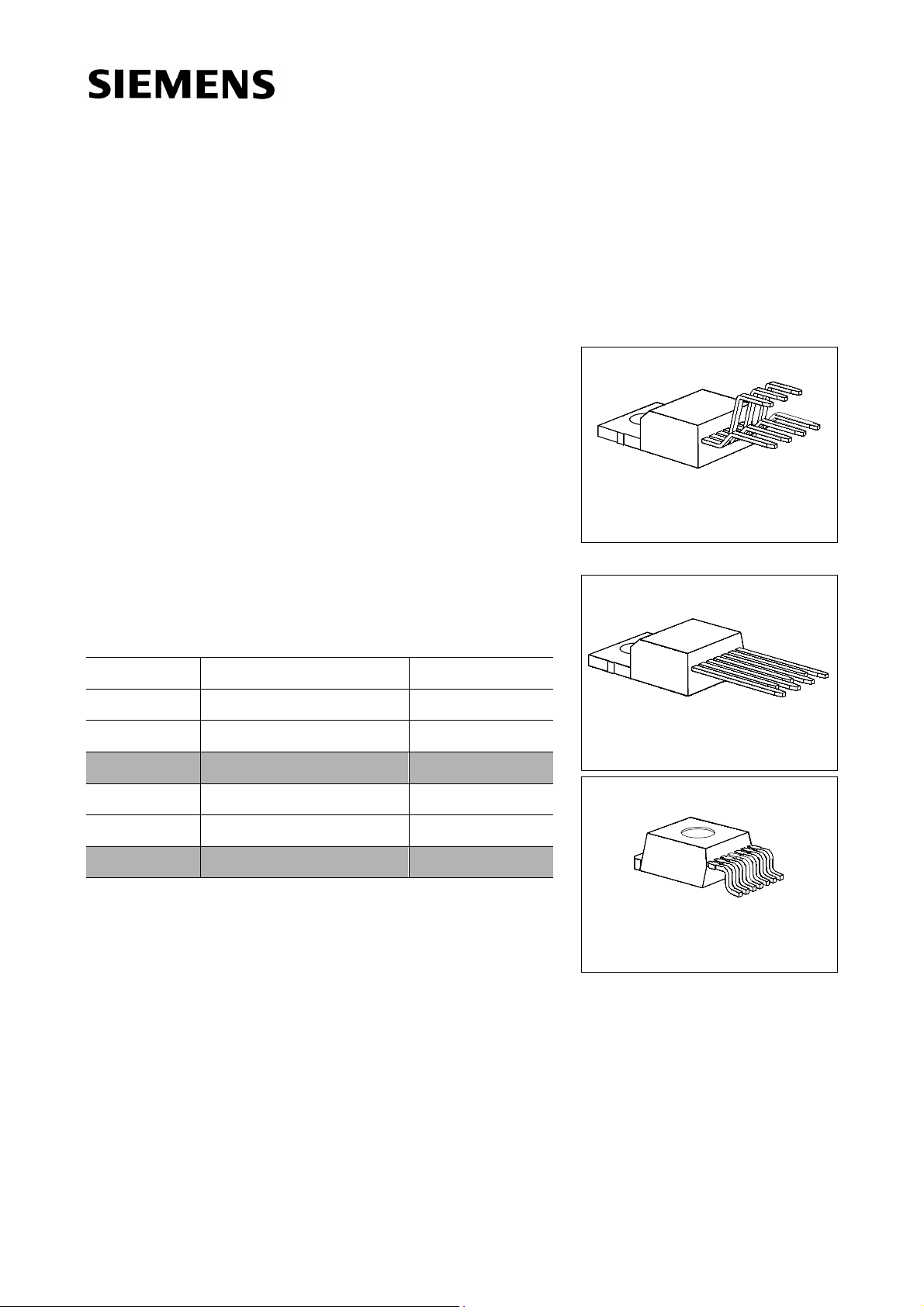
P-TO220-7-11
(P-TO220-7-1)
Type Ordering Code Package
TLE 4271 Q67000-A9210-A901 P-TO220-7-11
TLE 4271 S Q67000-A9244-A901 P-TO220-7-12
P-TO220-7-12
(P-TO220-7-2)
TLE 4271 G Q67006-A9195-A901 P-TO263-7-1
▼ TLE 4271 Q67000-A9210-C801 P-TO220-7-1
▼ TLE 4271 S Q67000-A9244-A801 P-TO220-7-2
TLE 4271 G Q67006-A9195-A801 P-TO220-7-8
▼
▼ Not for new design
P-TO263-7-1
(P-TO220-7-8)
Functional Description
This device is a 5-V low-drop fixed-voltage regulator. The maximum input voltage is 42 V
(65 V, ≤ 400 ms). Up to an input voltage of 26 V and for an output current up to 550 mA
it regulates the output voltage within a 2 % accuracy. The s hort circuit pro tection limits
the output current of more than 650 mA. The IC can be switched off via the inhibit input.
An integrated watchdog monitors the connected controller. The device incorporates
overvoltage protection and temperature protection that disables the circuit at
unpermissibly high temperatures.
Semiconductor Group 1 1998-11-01
Page 2
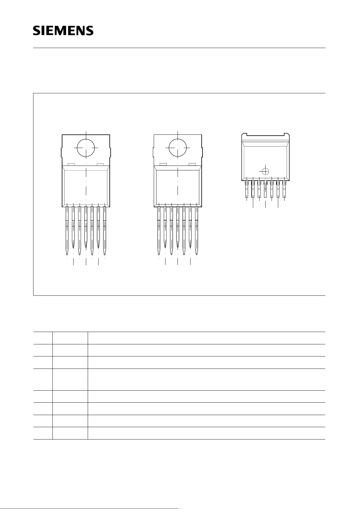
Pin Configuration
AEP01939
GNDINH
Ι
ROWD
Q
17
(top view)
TLE 4271
P-TO220-7-11
(P-TO220-7-1)
P-TO220-7-12
(P-TO220-7-2)
1
Ι
RO
GNDINH
Q
D
W
AEP02017
P-TO263-7-1
(P-TO220-7-8)
17
Q
Ι
7
INHROGND
D
W
AEP01938
Figure 1
Pin Definitions and Functions
Pin Symbol Function
1 I Input; block to ground directly on the IC with ceramic capacitor.
2INH Inhibit
3RO Reset Output; the open collector output is connected to the 5 V output
via an integrated resistor of 30 kΩ.
4GNDGround
5D Reset Delay; connect a capacitor to ground for delay time adjustment.
6W Watchdog Input
7Q 5-V Output; block to ground with 22 µF capacitor, ESR < 3 Ω.
Semiconductor Group 2 1998-11-01
Page 3

TLE 4271
Application Description
V
The IC regulates an input voltage in the range of 5 .5 V <
< 36 V to V
I
to 26 V it produces a regulated output current of more than 55 0 mA. Above 26 V the
save-operating-area protection allows operation up to 36 V with a regulated output
current of more than 300 mA. Overvoltage protection limits operation at 42 V. The
overvoltage protection hysteresis restores operation if the input voltage has dropped
below 36 V. The IC can be switched off via the inhibit input, which causes the quiescent
current to drop below 50 µA. A reset signal is generated for an output voltage of
V
< 4.5 V. The watchdog circuit monitors a connected controller. If there is no positive-
Q
going edge at the watchdog input wit hin a fixed time, the reset output is set to low. The
delay for power-on reset and the maximum permitted watchdog-pulse period can be set
externally with a capacitor.
Design Notes for External Components
= 5.0 V. Up
Qnom
C
An input capacitor
is necessary for compensation of lin e influences. The resonant
I
circuit consisting of lead inductance and input capacitance can be damped by a resistor
C
of approx. 1 Ω in series with
the regulating circuit. Stability is guaranteed at values of
. An output capacitor CQ is necessary for the stability of
I
C
≥ 22 µF and an ESR of
Q
<3Ω.
Circuit Description
The control amplifier compares a reference voltage, which is kept highly accurate by
resistance adjustment, to a volt age that is proportion al to the output voltag e and drives
the base of a series transistor via a buffer. Saturation control as a function of the load
current prevents any over-saturation of the power element.
C
If the output voltage decreases below 4.5 V, an external capacitor
discharged by the res et gene rator. If the voltage on th is capacitor
on pin 4 (D) will be
D
V
drops below V
D
DRL
a reset signal is generated on pin 2 (RO), i.e. reset output is set low. If the output voltage
C
rises above 4.5 V,
V
reaches VDU and the reset output w ill be set high again . The value of the power-on-
D
reset time can be set within a wide range depending on the capacity of
will be charged with constant current. After the power-on-reset time
D
C
. The value of
D
the pull-up resistor at reset output is typically 30 kΩ.
,
V
After
enabled and discharges
observed at watchdog input,
low and the watchdog c ircuit will b e disabled.
power-on reset until
If a watchdog pulse will be observed before
circuit will be enabled and
has reached the voltage VDU and reset was set to high, the watchd og circuit is
D
C
with a constant current. If there is no positiv e-going edge
D
C
will be discharged down t o V
D
C
will be charged with the current as at
D
V
reaches VDU and reset will be set high again.
D
C
is discharged down to V
D
C
will be charged too, b ut reset will n ot be se t low. After V
D
. Then reset will be set
DWL
, the watchdog
DWL
has reached VDU, the periodical behavior starts again.
Semiconductor Group 3 1998-11-01
D
Page 4
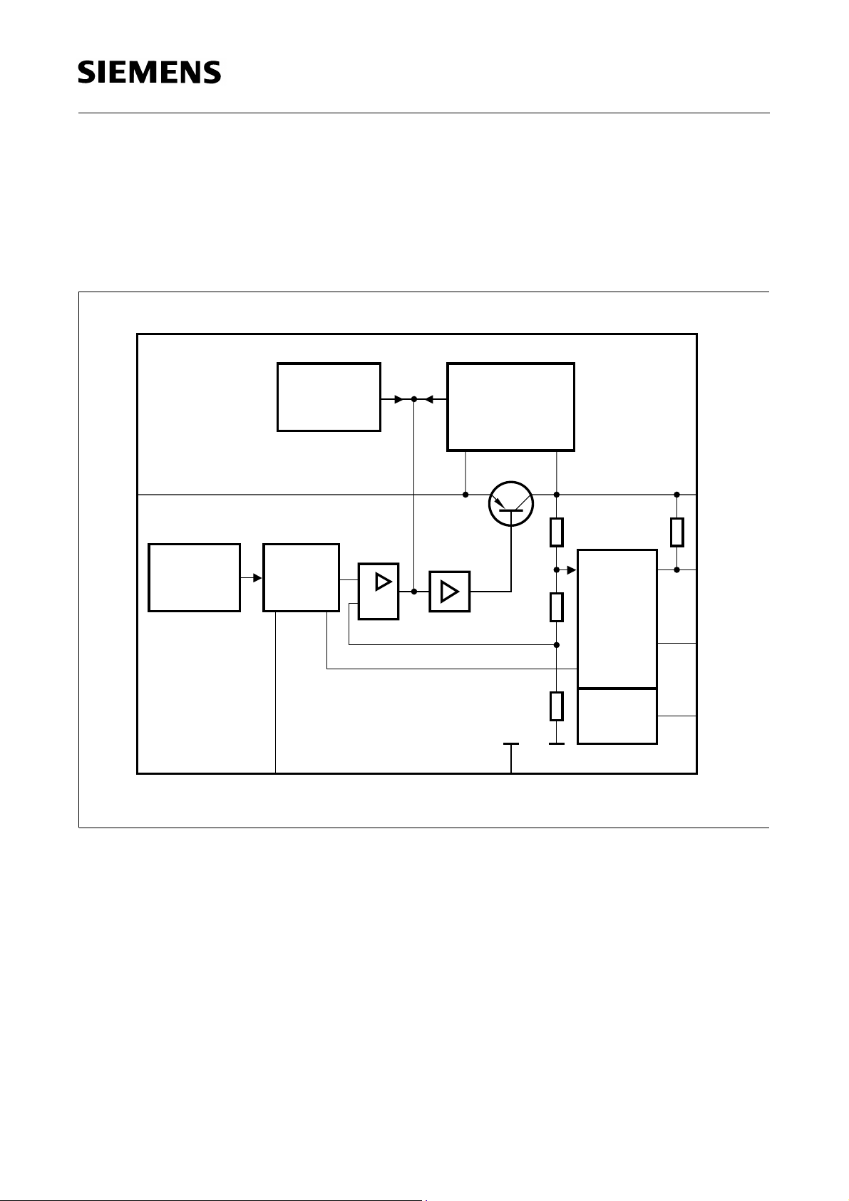
The IC also incorporates a number of internal circuits for protection against:
• Overload
• Overvoltage
• Overtemperature
• Reverse polarity
TLE 4271
1
Ι
Adjustment
Temperature
Sensor
Control
Amplifier
Bandgap
Reference
INH GND
+
-
Buffer
Saturation
Control and
Protection
Circuit
42
Reset
Generator
Watchdog
7
Q
3
R
5
D
6
W
AEB01940
Figure 2
Block Diagram
Semiconductor Group 4 1998-11-01
Page 5
Absolute Maximum Ratings
T
= – 40 to 150 °C
j
Parameter Symbol Limit Values Unit Notes
min. max.
Input
TLE 4271
Voltage
Voltage
Current
Inhibit
Voltage
Voltage
Current
Reset Output
Voltage
Current
Reset Delay
Voltage
Current
V
V
I
V
V
I
V
I
V
I
I
I
I
E
E
E
R
R
D
D
– 42
–
–
– 42
–
–
– 0.3
–
– 0.3
– 5
42
65
–
42
65
–
42
–
7
5
V
V
mA
V
V
mA
V
mA
V
mA
–
t ≤ 400 ms
internally limited
–
t ≤ 400 ms
internally limited
–
internally limited
–
–
Watchdog
Voltage
Current
V
I
W
W
– 0.3
– 5
7
5
V
mA
–
–
Output
Voltage
Current
V
I
Q
Q
– 1.0
– 5
16
–
V
mA
–
internally limited
Ground
Current
I
GND
– 0.5 – A –
Temperat ures
Junction temperature
Storage temperature
Semiconductor Group 5 1998-11-01
T
j
T
stg
–
– 50
150
150
°C
°C
–
–
Page 6
TLE 4271
Optimum reliability and life time are guaranteed if the junction temperature does not
exceed 125 °C in operating mode. Operation at up to the maximum junction temperature
of 150 °C is possible in principle. Note, however, that operation at the maximum
permitted ratings could affect the reliability of the device.
Operating Range
Parameter Symbol Limit Values Unit Notes
min. max.
Input voltage
Junction temperature
Thermal Resistance
Junction ambient
Junction case
V
T
R
R
Z
I
j
thja
thjc
thjc
640V–
– 40 150 °C–
–6570K/W
K/W–SMD version
–
–
–
3
6
2
K/W
K/W
K/W
–
P-TO220-7-8
t < 1ms
Semiconductor Group 6 1998-11-01
Page 7

TLE 4271
Characteristics
V
= 13.5 V; – 40 °C ≤ Tj= ≤ 125 °C (unless otherwise specified)
I
Parameter Symbol Limit Values Unit Test Condition
min. typ. max.
Output voltage
Output voltage
Output current
limiting
Current
consumption
I
= I
q
I
Current
consumption
I
= I
q
I
Current
consumption
I
= II– I
q
Q
Current
consumption
I
= II– I
q
Q
V
V
I
Qmax
I
q
I
q
I
q
I
q
Q
Q
4.90 5.00 5.10 V 5 mA ≤ IQ≤ 550 mA;
V
6 V ≤
≤ 26 V
I
4.90 5.00 5.10 V 26 V ≤ VI≤ 36 V;
I
≤ 300 mA;
Q
650 800 – mA VQ = 0 V
––50µA Ve = 0 V; IQ = 0 mA
– 800 – µA Ve = 5 V; IQ = 0 mA
–11.5mAIQ = 5 mA
–5575mAIQ = 550 mA
Current
I
q
–7090mAIQ = 550 mA; VI = 5 V
consumption
I
= II– I
q
Drop voltage
Load regulation ∆V
Supply voltage
regulation
Power supply
Ripple rejection
1)
Drop voltage = VI– VQ (measured when the output voltage has dropped 100 mV from the nominal value
obtained at 13.5 V input)
Q
V
dr
∆V
Q
Q
– 350 700 mV IQ = 550 mA
–2550mVIQ = 5 to 550 mA;
–1225mVVI = 6 to 26 V
PSRR –54–dBf
V
= 6 V
I
I
= 5 mA
Q
=100Hz;
r
V
=0.5V
r
1)
SS
Semiconductor Group 7 1998-11-01
Page 8

TLE 4271
Characteristics (cont’d)
V
= 13.5 V; – 40 °C ≤ Tj= ≤ 125 °C (unless otherwise specified)
I
Parameter Symbol Limit Values Unit Test Condition
min. typ. max.
Reset Generator
Switching threshold
Reset hi gh voltage
Reset low voltage
Reset low voltage
Reset pull-up
Lower reset timing
V
V
V
V
R
V
threshold
Charge current I
Upper timing
d
V
threshold
Delay time
Reset reaction time
t
d
t
RR
Overvoltage Protection
RT
ROH
ROL
ROL
DRL
DU
4.5 4.65 4.8 V –
4.5 – – V –
–60–mVR
=30 kΩ2);
intern
1.0 V ≤
V
Q
≤ 4.5 V
– 200 400 mV IR = 3 mA, VQ = 4.4 V
18 30 46 KΩ internally connection
to Q3
0.2 0.45 0.8 V VQ< V
RT
81425µA VD = 1.0 V
1.4 1.8 2.3 V –
81318msCD = 100 nF
––3µs CD = 100 nF
Turn-Off voltage
V
I, ov
40 44 46 V –
Inhibit
Inhibit ON voltage
Inhibit OFF voltage
Inhibit current
V
V
I
INH
INH
INH
1.0 2.0 3.5 V VQ = high (> 4.5 V)
0.8 1.3 3.3 V VQ = low (< 0.8 V)
81225µA V
INH
= 5 V
Watchdog
Upper timing
V
DU
1.4 1.8 2.3 V –
threshold
Lower watchdog
V
DWL
0.2 0.45 0.8 V –
timing threshold
Discharge current
Semiconductor Group 8 1998-11-01
I
dis
1.5 2.7 3.5 µA VD = 1 V
Page 9

TLE 4271
Characteristics (cont’d)
V
= 13.5 V; – 40 °C ≤ Tj= ≤ 125 °C (unless otherwise specified)
I
Parameter Symbol Limit Values Unit Test Condition
min. typ. max.
Charge current I
Watchdog period
Watchdog trigger
d
t
w
t
wt
time
Watchdog pulse
V
W
slew rate
2)
Reset peak is always lower than 1. 0 V.
81425µA VD = 1 V
40 55 75 ms CD = 100 nF
30 45 66 ms CD = 100 nF
see diagr am
5 ––V/µs from 20% to 80% V
Q
Semiconductor Group 9 1998-11-01
Page 10

TLE 4271
Figure 3
Test Circuit
V
Ι
Ι
Ι
µ
1000 F
470 nF
V
INH
Ι
17
Q
µ
22 F
TLE 4271
Ι
R
32
V
5
Ι
D
V
D
C
6
V
W
D
4
Ι
GND
V
Q
R
AES01941
Input
1
7
5 V-Output
470 nF
Input
e.g. KL 15
Reset
2
3
TLE 4271
22 F
µ
5
to MC
4
6
100 nF
AES01942
Figure 4
Application Circuit
Semiconductor Group 10 1998-11-01
Page 11
TLE 4271
V
Ι
t
<
RR
V
Q
V
RT
d
Ι
V
d
=
d
C
V
V
DU
D
V
DRL
tt
d
V
R
RR
t
d
Power-on-Reset
Figure 5
Time Response
V
W
V
Ι
V
Q
V
V
DU
D
V
DWL
V
R
Thermal
Voltage Drop Undervoltage
Shutdown at Input
Secondary Load
Spike
t
wt
t
wr
Bounce
t
w
AES01927
Ι
V
V
( ) ( )
-
DU
=
t
w
=
t
wt
DWL
Ι
dxdis
V
V
-
DU
DWL
Ι
dis
ΙΙ
Ι
+
dis
d
C
C
D
=
t
wr
V
V
-
DU
DWL
d
= (Watchdog Reset Time)
C
DD
AES01943
Figure 6
Time Response, Watchdog Behavior
Semiconductor Group 11 1998-11-01
Page 12

TLE 4271
j
Output Voltage VQ versus
Temperature
5.20
V
V
Q
5.10
5.00
4.90
4.80
4.70
4.60
T
= 13.5 V
V
Ι
j
40-40 0
80 120
AED01928
160
C
T
j
Output Voltage VQ versus
Input Voltage
12
V
V
Q
10
8
6
4
2
0
0
2
V
I (VI
4
= Ve)
R
= 25
Ω
L
68
AED01929
10
V
V
Ι
Output Current IQ versus
Temperature
1200
mA
Ι
Q
1000
800
600
400
200
0
T
j
40-40 0
AED01930
80 120
T
C
160
Output Current
Input Voltage
1.2
A
Ι
Q
1.0
0.8
0.6
T
j
0.4
0.2
0
I
versus
Q
V
I
= 125 C
20010
30
T
= 25 C
j
AED01931
40
50
V
V
Ι
Semiconductor Group 12 1998-11-01
Page 13
TLE 4271
AED01932
Current Consumption I
versus Output Current I
6
mA
Ι
q
5
4
3
V
= 13.5 V
Ι
2
1
0020 1206040
q
Q
Current Consumption I
versus Output Current I
q
Q
AED01933
80
mA
Ι
q
70
60
50
V
= 13.5 V
Ι
40
30
20
10
80
mA
Ι
Q
0
1000 200
400 600
300
mA
Ι
Q
Current Consumption I
versus Input Voltage V
120
mA
Ι
q
100
80
60
R
L
40
= 20
R
20
0
Ω
L
20010
q
I
= 10
R
30
Ω
= 50
L
40
AED01934
Ω
50
V
V
Ι
Drop Voltage Vdr versus
Output Current
800
mV
V
Dr
700
600
500
T
= 125 C
j
400
300
200
100
0
2000 400
I
Q
T
600 1000
j
=25
AED01935
C
mA
Ι
Q
Semiconductor Group 13 1998-11-01
Page 14

TLE 4271
Inhibit Current IE
versus Inhibit Voltage
12
µ
A
Ι
E
10
Ι
8
6
4
2
0
0
Ι
e, off
1
2
V
e, on
3
E
Ι
e, high
V
= 13.5 V
Ι
T
= 25 C
j
4
AED01944
5
6
V
V
E
Output Voltage V
Q
versus Inhibit Voltage V
6
V
V
Q
5
4
3
2
1
0
0
21
V
T
3
E
AED01945
= 13.5 V
Ι
= 25 C
j
4
V
5
6
V
E
Inhibit Current Consumptions Ie
versus Temperature
14
A
µ
Ι
e
12
10
8
6
4
2
0
-40
0 1208040
T
j
Ι
e, high
Ι
e, on
Ι
e, off
AED01946
T
j
160
Inhibit Voltages V
e
versus Temperature T
6
V
V
e
5
4
3
2
1
V
e, off
0
40-40 0
j
AED01947
V
e, on
80 120
T
j
C
160
Semiconductor Group 14 1998-11-01
Page 15
TLE 4271
j
Switching Voltage VDU and V
DWL
40-40 0
T
j
V
Ι
= 13.5 V
V
DU
80 120
versus Temperature
2.4
V
V
2.0
1.6
1.2
0.8
0.4
V
0
DWL
AED01948
160
C
T
j
Charge Current Id and Discharge
I
Current
16
A
µ
Ι
14
12
10
8
6
4
2
8
-40
versus Temperature T
dis
AED01949
Ι
d
V
= 13.5 V
Ι
V
= 1 V
D
Ι
dis
400
80
C
160120
T
j
Watchdog Pulse Time Tw
versus Temperature
80
ms
T
W
70
60
50
40
30
20
10
0
-40
T
V
= 13.5 V
Ι
C
= 100 nF
D
400
j
80
AED01950
160120
C
T
j
Semiconductor Group 15 1998-11-01
Page 16

Package Outlines
P-TO220-7-1
(Plastic Transistor Single Outline Package)
TLE 4271
+0.4
10
10.2
-0.2
+0.1
3.75
2.8
17
1.27
1)
+0.1
0.6
1) 0.75
1) 0.75
at dam bar (max 1.8 from body)
-0.15
im Dichtstegbereich (max 1.8 vom Körper)
-0.15
0.6
7x
4.6
-0.2
1 x 45˚
+0.1
1.27
±0.3
-0.2
±0.4
19.5 max
16
2.6
+0.1
0.4
±0.4
M
4.5
8.4
±0.4
8.8
15.4
±0.3
±0.3
8.6
10.2
GPT05108
Sorts of Packing
Package outlines for tubes, trays etc. are contained in our
Data Book “Package Information”.
Dimensions in mm
Semiconductor Group 16 1998-11-01
Page 17

P-TO220-7-2
(Plastic Transistor Single Outline Package)
+0.4
10
10.2
-0.2
+0.1
3.75
2.8
1.27
+0.1
4.6
-0.2
1 x 45˚
-0.2
8.8
TLE 4271
15.4
17
11
1.27
+0.1
1)
0.6
1) 0.75
1) 0.75
at dam bar (max 1.8 from body)
-0.15
im Dichtstegbereich (max 1.8 vom Körper)
-0.15
13
0.6
7x
+0.1
0.4
M
2.6
GPT05257
Sorts of Packing
Package outlines for tubes, trays etc. are contained in our
Data Book “Package Information”.
Dimensions in mm
Semiconductor Group 17 1998-11-01
Page 18

P-TO220-7-11
(Plastic Transistor Single Outline Package)
±0.2
±0.3
17
1)
±0.3
13.4
15.65
C
0...0.15
10
9.8
8.5
3.7
1.27
±0.15
1)
-0.15
7x
0.6
A
±0.2
2.8
±0.3
8.6
±0.1
±0.3
10.2
M
TLE 4271
4.4
±0.1
1.27
0.05
±0.3
3.7
2.4
A0.25
C
8.4
±0.4
±0.2
9.25
0.5
3.9
±0.1
±0.4
1)
Typical
All metal surfaces tin plated, except area of cut.
GPT09083
Sorts of Packing
Package outlines for tubes, trays etc. are contained in our
Data Book “Package Information”.
Dimensions in mm
Semiconductor Group 18 1998-11-01
Page 19

P-TO220-7-12
(Plastic Transistor Single Outline Package)
±0.2
±0.3
17
1)
±0.3
15.65
13.4
10
9.8
8.5
3.7
±0.15
1)
-0.15
A
±0.2
2.8
1.27
0.05
TLE 4271
B
4.4
±0.1
±0.2
9.25
±0.5
7x
0.6
11
±0.1
±0.5
13
2.4
M
BA0.25
C
C
0...0.15
1)
Typical
1.27
All metal surfaces tin plated, except area of cut.
±0.1
0.5
GPT09084
Sorts of Packing
Package outlines for tubes, trays etc. are contained in our
Data Book “Package Information”.
Dimensions in mm
Semiconductor Group 19 1998-11-01
Page 20

P-TO263-7-1
(Plastic Transistor Single Outline Package)
±0.2
10
±0.15
9.8
A
1)
8.5
±0.3
1
1)
8
0...0.15
6x1.27
(15)
7x0.6
±0.2
9.25
±0.1
TLE 4271
4.4
±0.1
1.27
B
0.1
2.4
±0.3
±0.5
2.7
4.7
0.5
8˚ max.
M
BA0.25
0.05
±0.1
0.1
1)
Typical
All metal surfaces tin plated, except area of cut.
P-TO220-7-8
(Plastic Transistor Single Outline Package)
10.2
8.0
10.1
0.6
1.27
6 x 1.27 = 7.62
GPT09114
4.6
1.27
0.2
2.6
1)
8.8
3.5
1.5
0.4
GPT05874
1) shear and punch direction burr free surface
Sorts of Packing
Package outlines for tubes, trays etc. are contained in
our Data Book “Package Information”.
SMD = Surface Mounted Device
Dimensions in mm
Semiconductor Group 20 1998-11-01
 Loading...