

Page 1
现货库存、技术资料、百科信息、热点资讯,精彩尽在鼎好!
Low Drop Voltage Tracker TLE 4251
Features
• Output tracking tolerance ≤ ± 0.2%
• 400 mA ou tput current capabi lity
• Enable Function
• Very low current consumption in OFF mode
• Wide operation range: up to 40 V
• Wide temperature range: – 40 °C ≤
• Output protected against short circuit
• Overtemperature protection
• Reverse polarity proof
T
≤ 150 °C
j
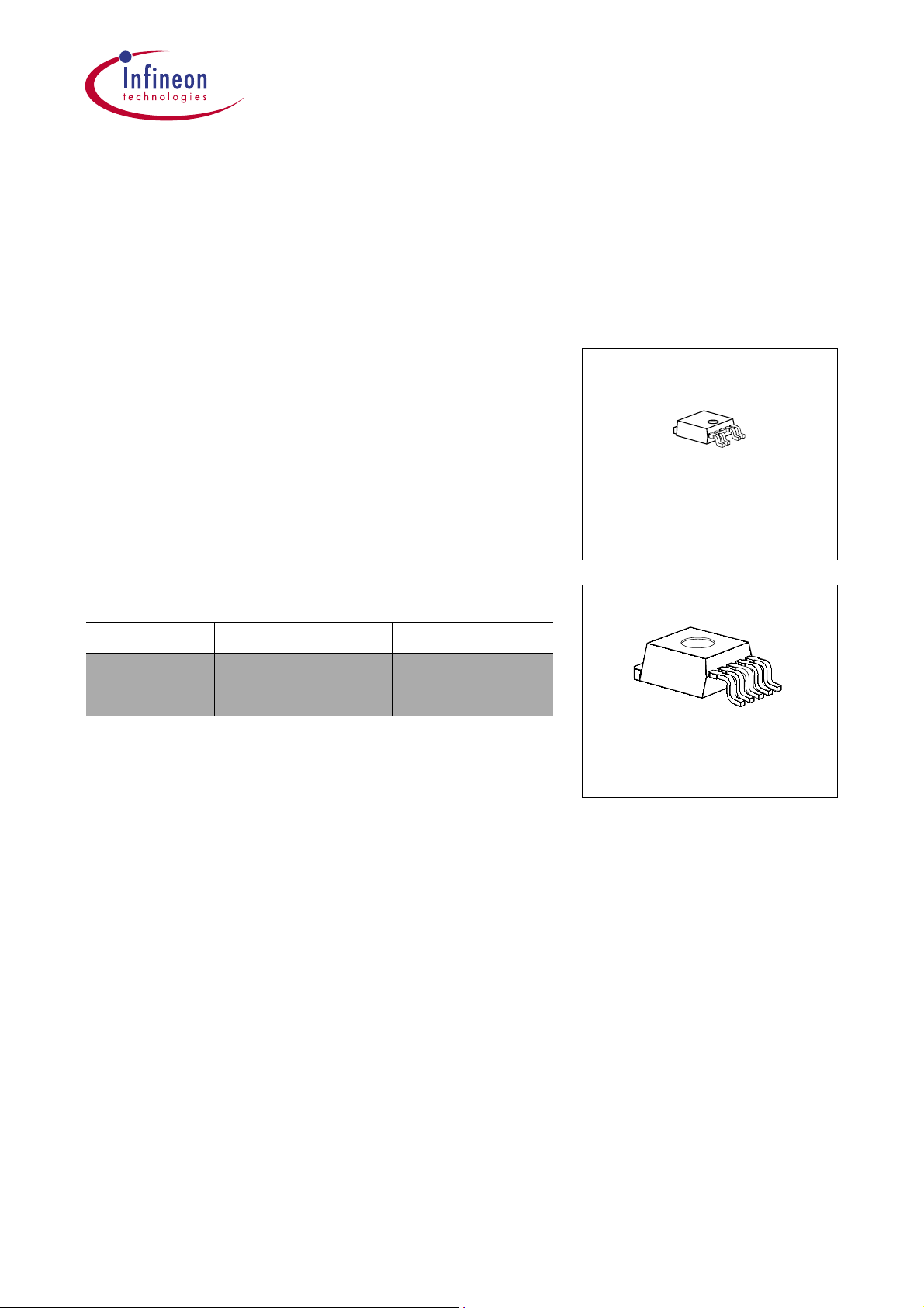
P-TO252-5-1
Type Ordering Code Package
TLE 4251 D Q67006-A9439 P-TO252-5-1
TLE 4251 G Q67006-A9529 P-TO263-5-1
P-TO263-5-1
Functional Description
The TLE 4251 is a monolithic integrated low-drop voltage tracker in the very small SMD
package P-TO252-5-1. It is designed to supply e.g. sensors under the severe conditions
of automotive appl ications. Therefore the device is equipped with additional protection
functions against over load, short circuit and reverse polarity.
Supply voltages up to 40 V are tracked to a reference vol tage given to the adjust input
via an exter nal resistor.
The output is able to drive loads up to 400 mA while it follows e.g. the 5 V output of a
main voltage regulator within an accuracy of 0.5%. For loads up to 300 mA the tracking
accuracy is 0.2%.
The TLE 4251 can be switched in stand-by mode via the enable EN input which causes
the current consumption to dr op to very low values. This feature makes the IC suitable
for low power battery applications.
Data Sheet Rev. 2.4 1 2001-05-07
Page 2
GND
TLE 4251
P-TO263-5-1P-TO252-5-1
1
EN
I
5
QADJ
AEP02810
1
GND
EN QADJ
I
5
AEP03119
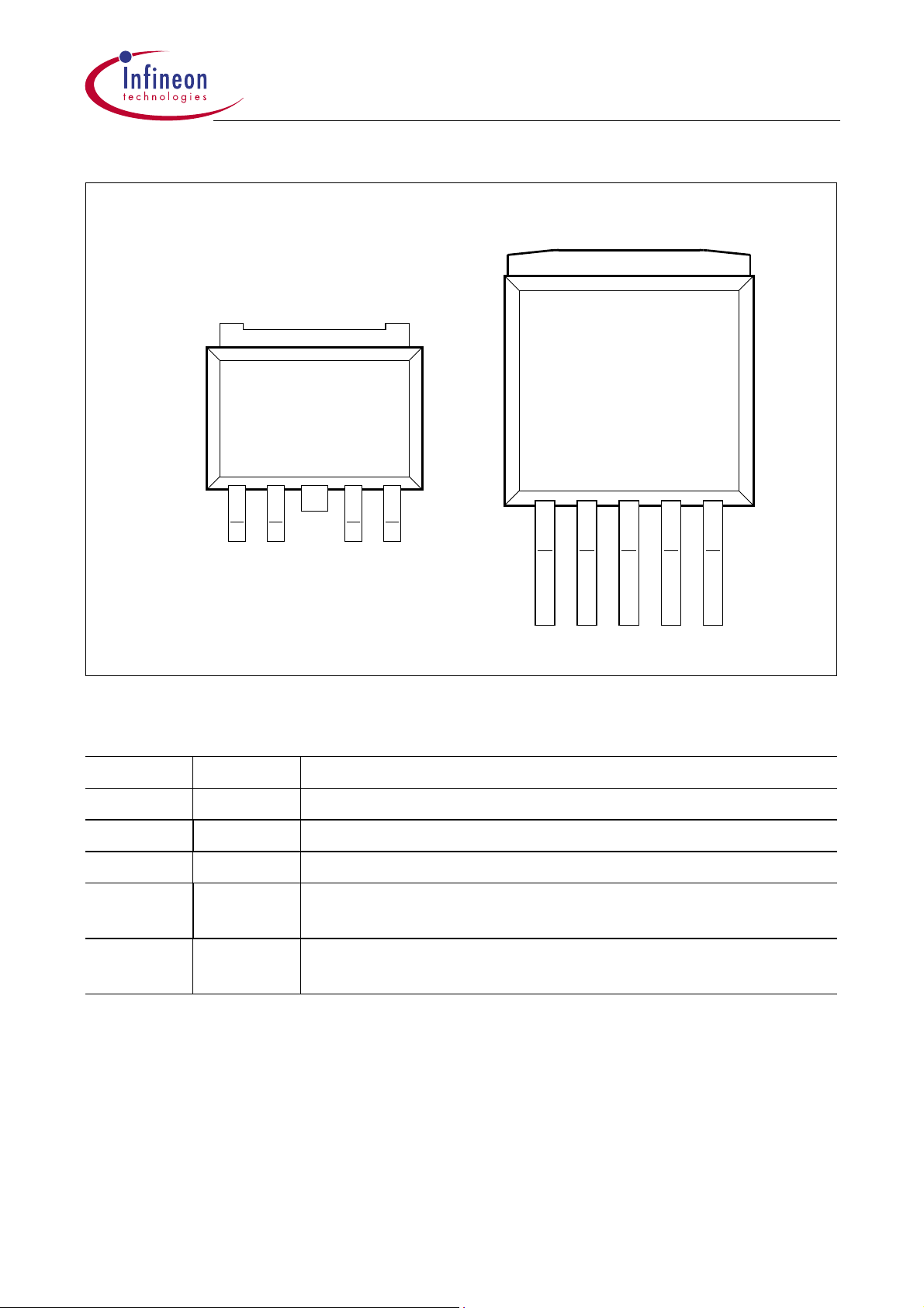
Figure 1 Pin Configuration (top view)
Pin No. Symbol Function
1IInput voltage
2ENEnable, high- active input
3GNDGround
4ADJAdjust; connect to the reference voltage via ext. resistor or
micro-controller port
5QOutput voltage; must be blocked by a capacitor
C
≥ 22 µF, ESR ≤ 3 Ω to GND
Q
Data Sheet Rev. 2.4 2 2001-05-07
Page 3
TLE 4251
I
Saturation
Control and
Protection
Circuit
TLE 4251
Temperature
Control
ADJ
EN
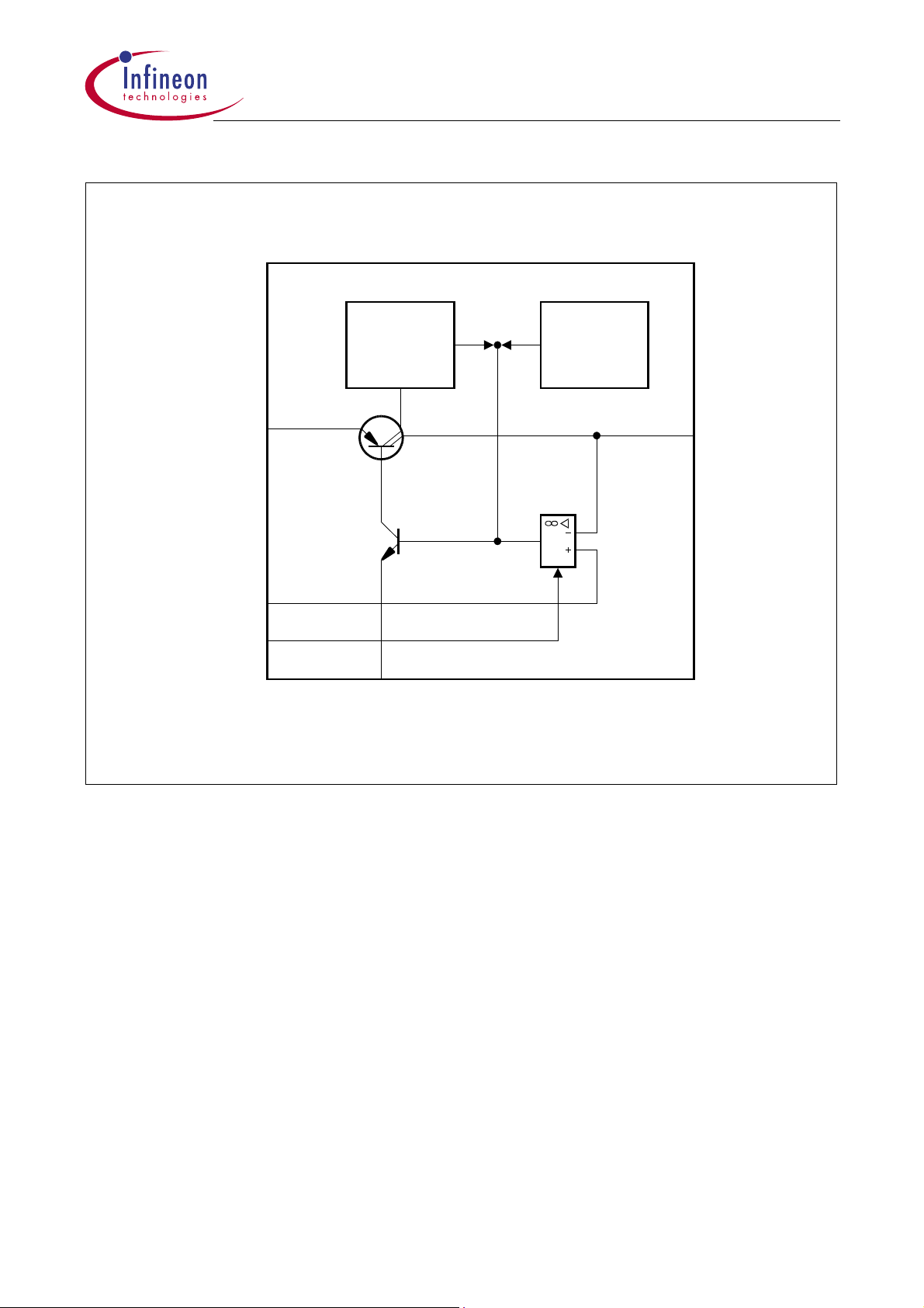
Figure 2 Block D iagram
GND
AES02807
Data Sheet Rev. 2.4 3 2001-05-07
Page 4
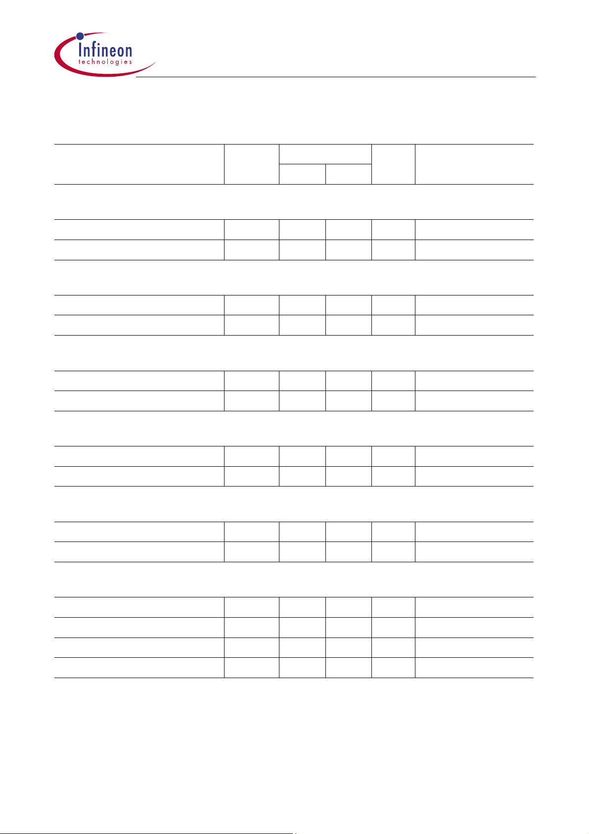
Absolute Maximum Ratings
T
– 40 °C<
< 150 °C
j
Parameter Symbol Limit Value s Unit Remarks
min. max.
Input
TLE 4251
Voltage
Current
Output
Voltage
Current
Adjust
Voltage
Current
Enable
Voltage
Current
Temperatures
V
I
V
I
V
I
V
I
I
I
Q
Q
ADJ
ADJ
EN
EN
– 42 45 V –
––mA internally limited
– 245 V –
––mA internally limited
– 42 45 V –
––µA internally limited
– 42 45 V –
––µA internally limited
Junction temperature
Storage te mperature
T
j
T
stg
– 40 150 °C –
– 50 150 °C –
Thermal Resistances
Junction case
Junction ambient
Junction case R
Junction ambient
1)
Worst case, regardingpeak temperature; zero airflow; mountedan a PCB 80 × 80 × 1.5 mm
300 mm
2
.
R
R
R
thjc
thja
thjc
thja
– 4 K/W TLE 4251 D
– 78 K/W TLE 4251 D
– 3 K/W TLE 4251 G
– 52 K/W TLE 4251 G
3
, heat sink area
1)
1)
Note: Maximum ratings are absolute ratings; exceeding any one of these values may
cause irreversible damage to the integrated circuit.
Data Sheet Rev. 2.4 4 2001-05-07
Page 5
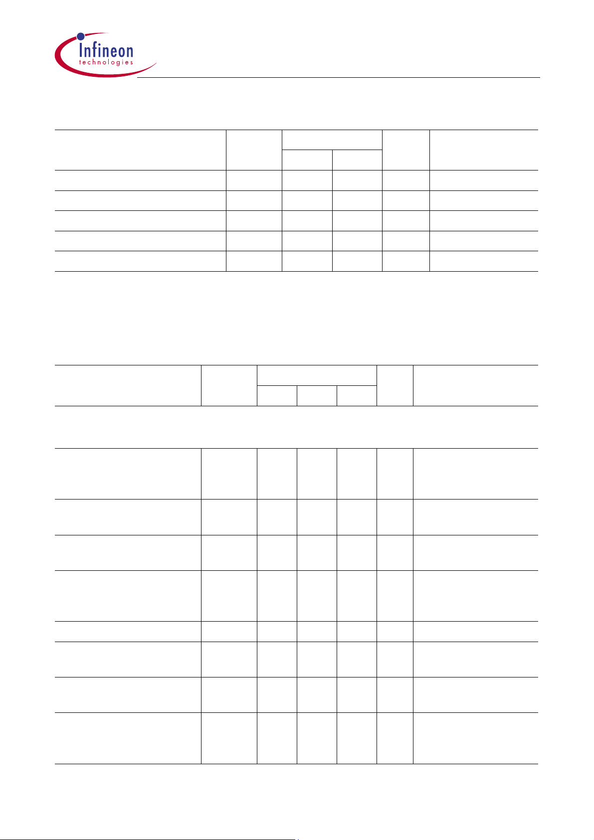
TLE 4251
Operating Range
Parameter Symbol Limit Values Unit Re marks
min. max.
Input voltage
V
I
1)
4
40 V –
Adjust input vo ltage
Adjust input vo ltage
Enable input voltag e V
Junction temperature
1)
V
> V
I
ADJ
+ V
DR
V
V
T
ADJ
ADJ
EN
j
2.5 40 V –
02.5VVQ ≤ V
040V–
– 40 150 °C –
ADJ
+ ∆V
Electrical Characteristics
V
= 13.5 V; 2.5 V ≤ V
I
≤ VI– 0.5 V; – 40 °C<Tj<150°C; unless otherwise specified
ADJ
Parameter Symbol Limit Values Unit Test Condition
min. typ. max.
Output
Output voltage tracking
accuracy
∆V
Q
= V
ADJ
– V
Q
∆V
Q
– 10 – 10 mV VI< 13.5 V;
– 40 °C<
T
<125°C;
j
1mA<IQ< 300 mA
Q
Output voltage tracking
∆V
accuracy
Output voltage tracking
∆V
accuracy
Drop voltage
V
Output current I
Output capacitor C
Q
Q
dr
Q
Q
– 10 – 10 mV 6 V < VI<40V
I
5mA<
< 200 mA
Q
– 25 – 25 mV 6 V < VI<28V
I
1mA<
< 300 mA
Q
– 280 520 mV IQ=300mA;
V
>4V;
ADJ
Enable ON;
400 450 800 mA Tj≤ 125 °C
1)
1)
22 ––µF ESR ≤ 3 Ω
at 10 kHz
Current consumption
I
= II– I
q
Q
Current consumption
I
= II– I
q
Data Sheet Rev. 2.4 5 2001-05-07
Q
I
q
I
q
– 10 20 mA IQ= 300 mA
– 230 300 µA IQ<1mA
T
<85°C
j
V
in ON state
EN
Page 6
TLE 4251
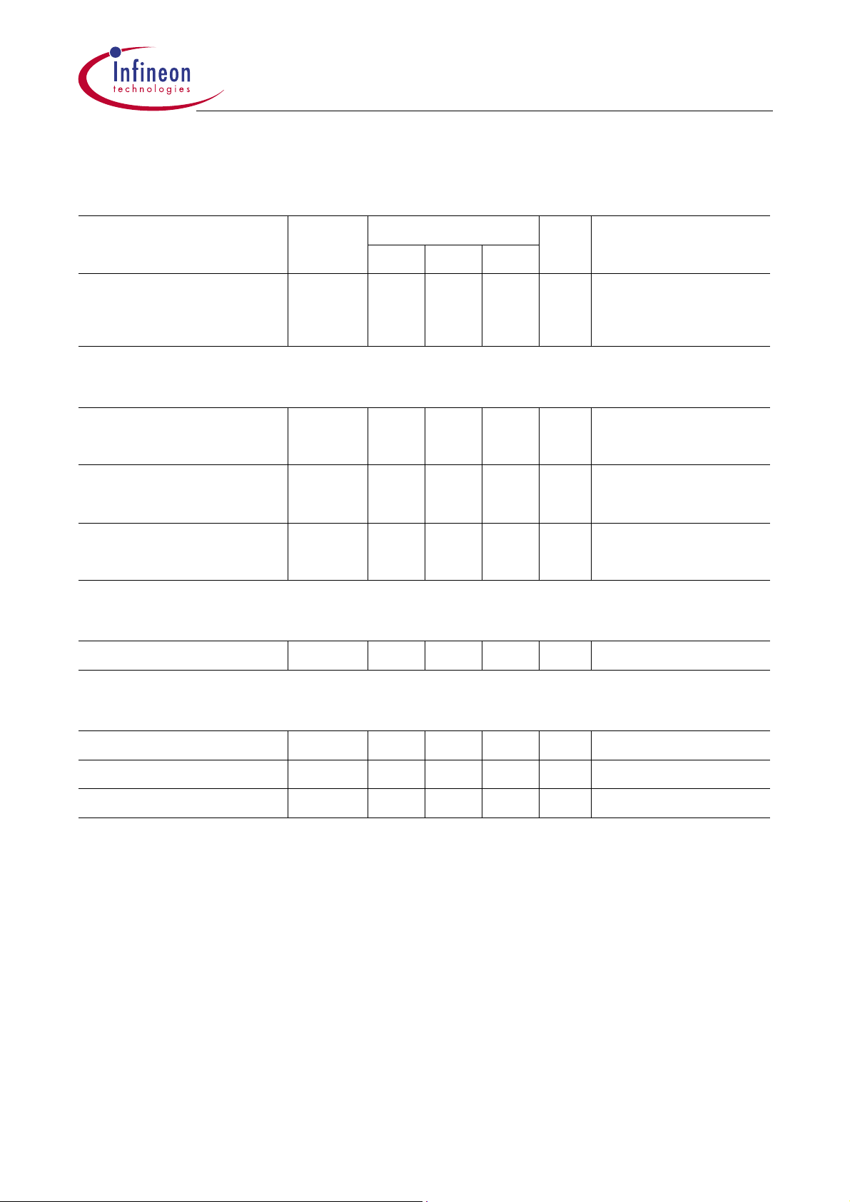
Electrical Characteristics (cont’d)
V
= 13.5 V; 2.5 V ≤ V
I
Parameter Symbol Limit Values Unit Test Condition
≤ VI– 0.5 V; – 40 °C<Tj<150°C; unless otherwise specified
ADJ
min. typ. max.
Quiescent current
(stand-by)
I
= II– I
q
Q
Regulator Performance
Load regulation
Line regul ation
Power-Supply-RippleRejection
Adjust Input
Input biasing current
I
q
∆V
Q
∆V
Q
PSRR
I
ADJ
– 010µA VEN=0V
T
<85°C
j
– 35 ± 535mV5mA<IQ< 300 mA;
V
– 25 ± 10 25 mV
=6V,V
I
12 V <
I
=5mA
Q
V
I
=5V
ADJ
<32V
60 ––dB fr=100Hz;
V
=5V
– 0.1 0.5 µA V
r
ADJ
PP
=5V
Enable
Enable on voltage range
Enable off voltage range
Input current
1)
Measured when the output voltage VQhas dropped 100 mV from the nominal value.
V
EN ON
V
EN OFF
I
EN
2 ––V VQON
––0.5 V VQ≤ 0.1 V
54070µA VEN=5V
Data Sheet Rev. 2.4 6 2001-05-07
Page 7
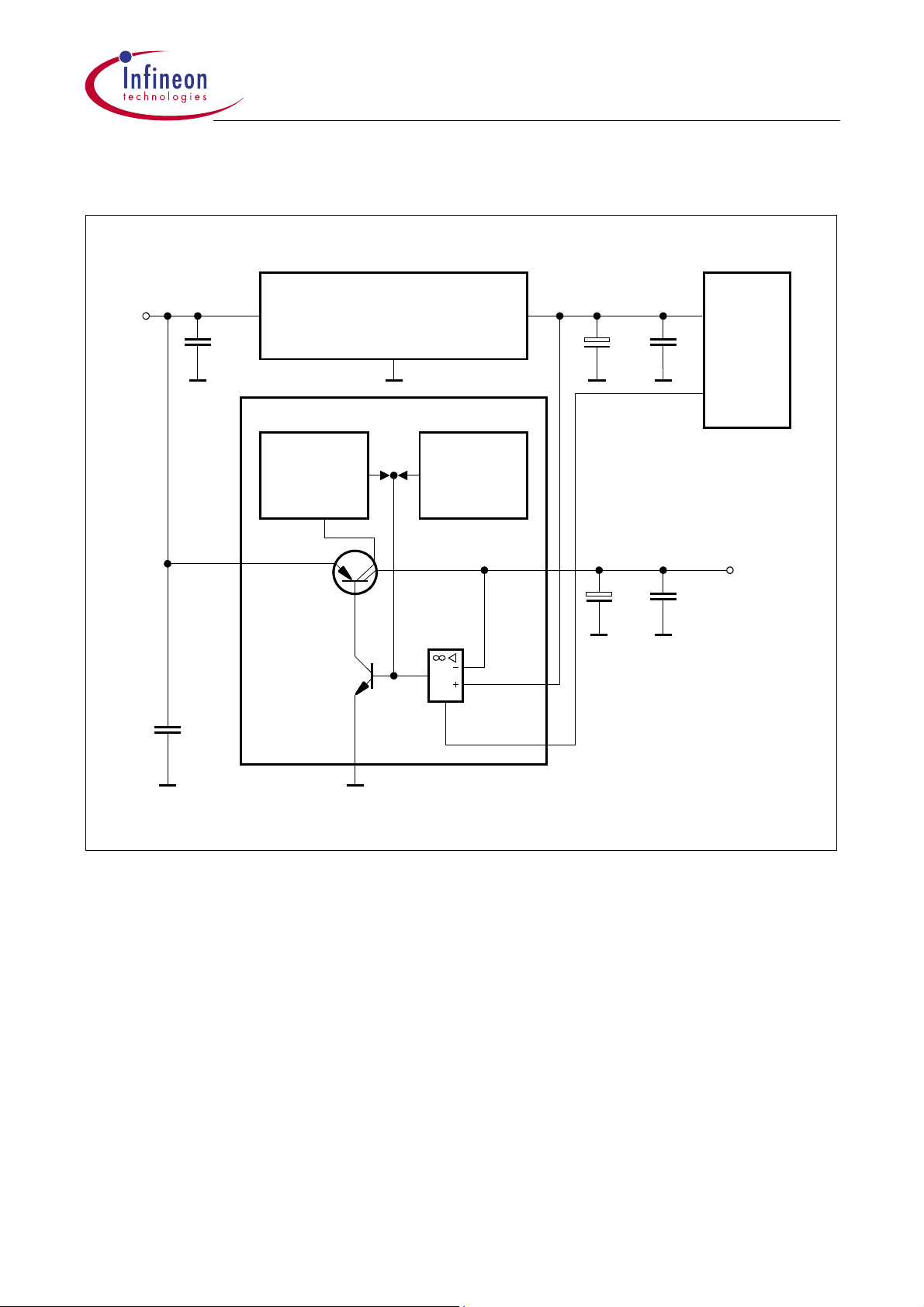
Application Information
TLE 4251
6...40 V
100 nF
C
100 nF
e.g. TLE 4470
I V
TLE 4251
Saturation
Control and
Protection
Circuit
TLE 4269
TLE 4278
GND
Temperature
Control
I
GND
Q
ADJ
EN
22 µF
Q
22 µF
100 nF
µC
CC
I/O
LOAD
to
sensor
Figure 3 Application Circuit
AES02808
Data Sheet Rev. 2.4 7 2001-05-07
Page 8
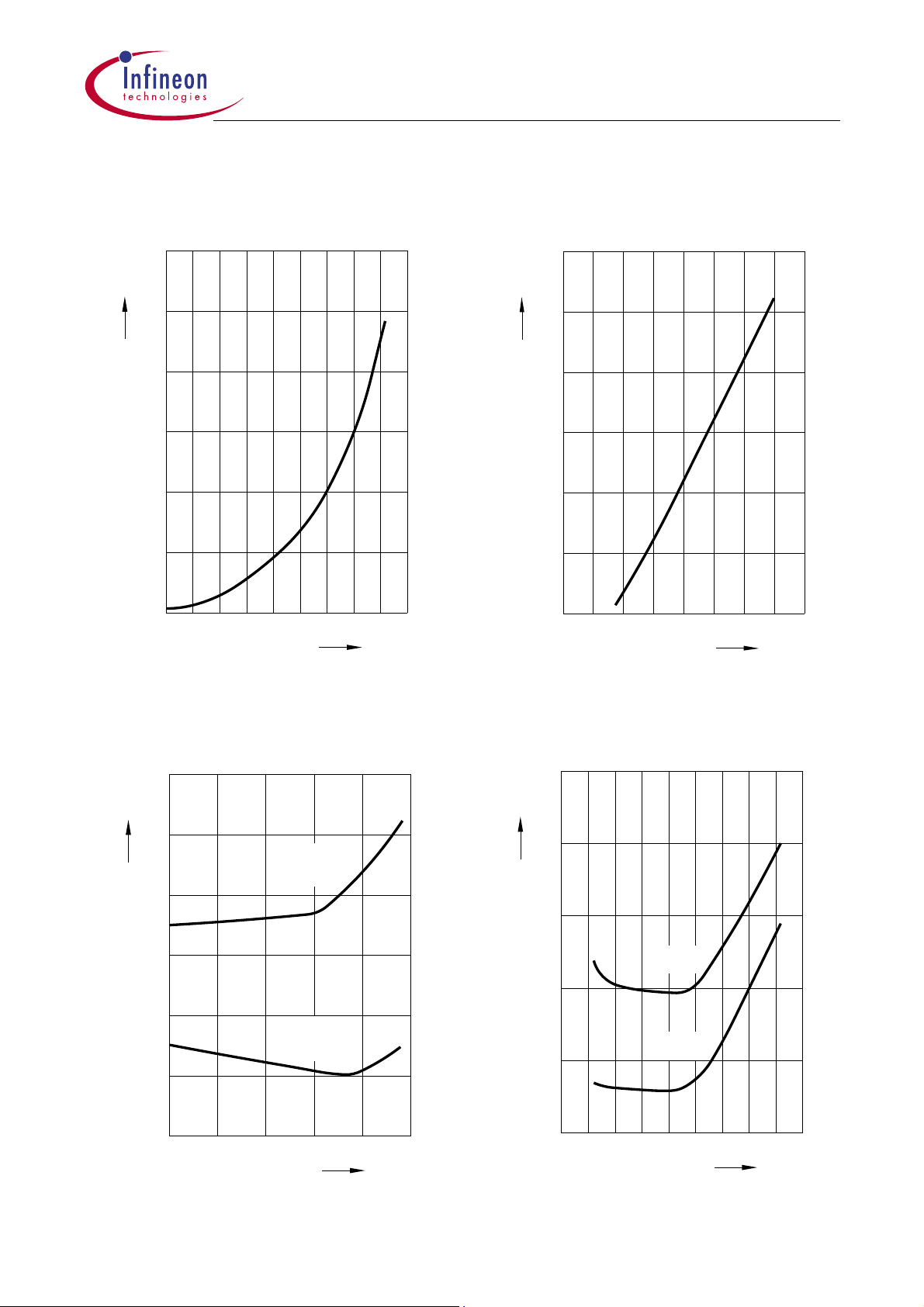
TLE 4251
Quiescent Current Iqversus
Output Current
30
I
mA
q
25
20
15
10
5
0
0
I
Q
100 200 300 mA 450
AED02900
I
Q
Enable Current IENversus
Enable Voltage
30
µA
I
ENABLE
25
20
15
10
5
0
0
V
EN
0.5 1 1.5 2 2.5 3 3.5 4V
AED02901
V
ENABLE
Tracking A ccuracy ∆VQversus
T
Temperature
6
mV
V
Q
4
2
0
-2
-4
-6
-40
, V
j
0
=5V
ADJ
V
=6V
I
= 300 mA
I
Q
V
=40V
I
I
= 200 mA
Q
40 80 120 160
AED02902
˚C
T
j
Current Consumption Iqversus
V
Input Voltage
400
I
µA
q
350
300
250
200
150
0
5 10 15 20 25 30 35 V 45
, V
I
ADJ
I
=10mA
Q
I
=1mA
Q
=5V
AED02904
V
Ι
Data Sheet Rev. 2.4 8 2001-05-07
Page 9
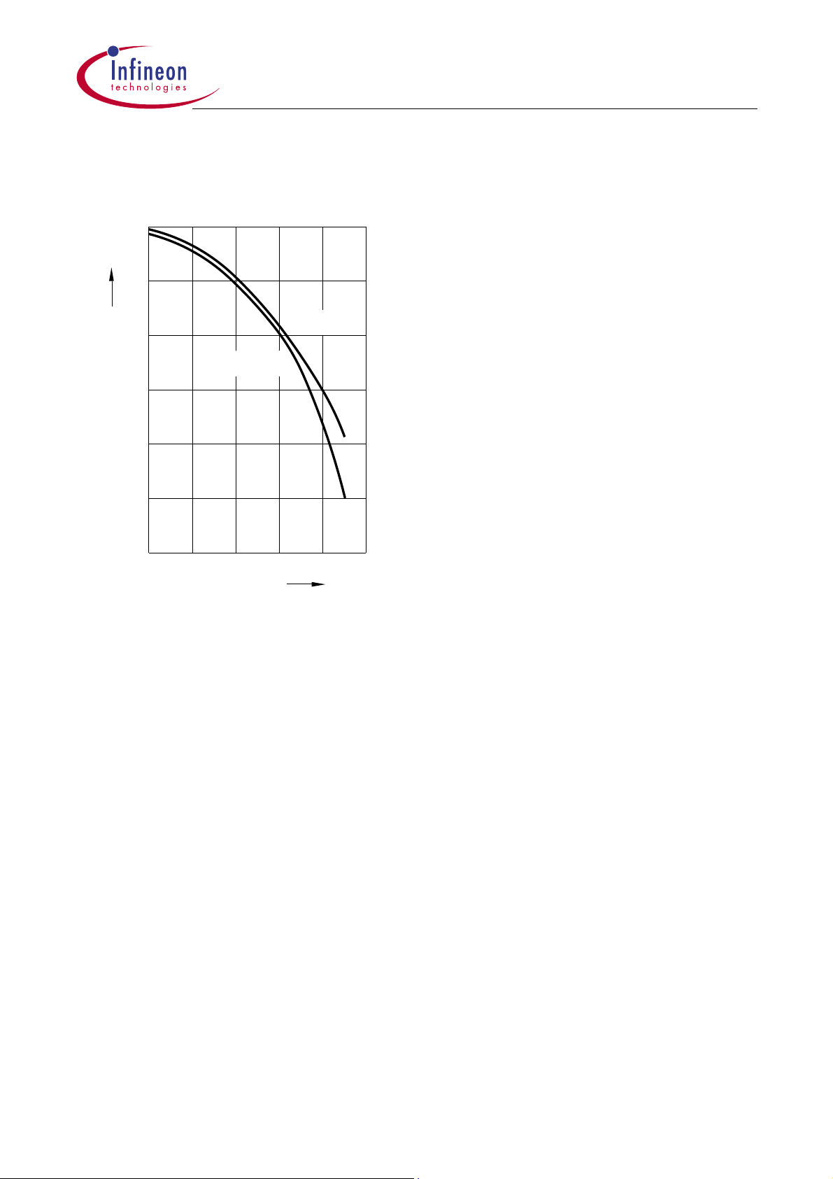
Tracking A ccuracy ∆VQversus
Output Current
I
Q
TLE 4251
3
mV
V
Q
AED02903
2.5
V
=5V
2
V
ADJ
ADJ
=3V
1.5
1
0.5
0
0
100
200 300 400 500
I
mA
Q
Data Sheet Rev. 2.4 9 2001-05-07
Page 10
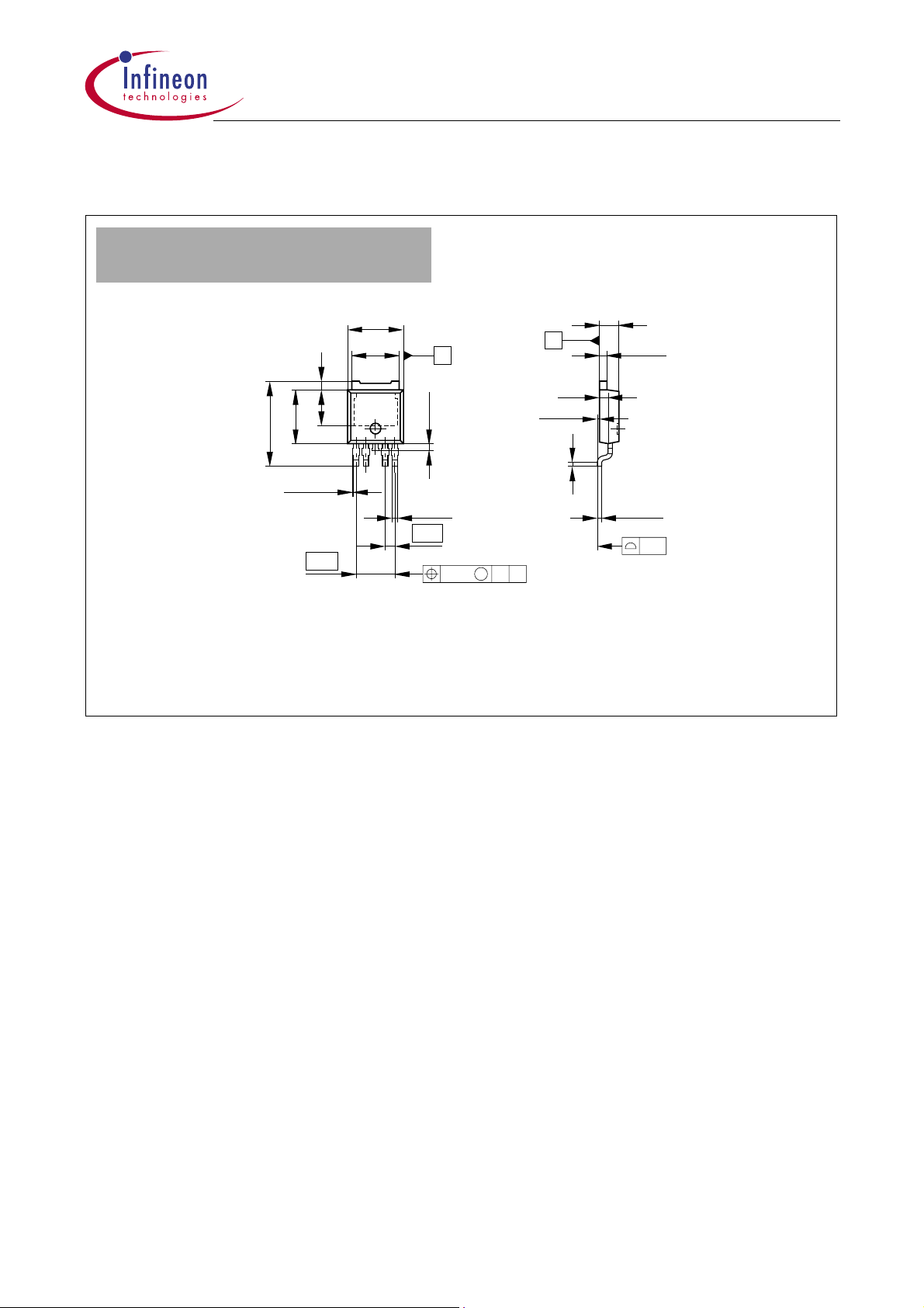
Package O utlines
P-TO252-5-1
(Plastic Transistor Single Outline)
TLE 4251
+0.15
6.5
-0.10
±0.1
±0.5
9.9
-0.2
6.22
±0.1
1
(4.17)
5.4
A
±0.15
0.8
0.15 max
per side
5x0.6
±0.1
1.14
4.56
M
A0.25
All metal surfaces tin plated, except area of cut.
B
B
±0.1
1
0...0.15
0.51 min
2.3
+0.05
-0.10
0.9
0.5
GPT09161
+0.08
-0.04
+0.08
-0.04
0.1
Data Sheet Rev. 2.4 10 2001-05-07
Page 11
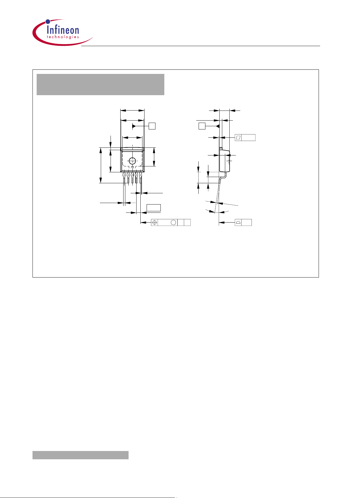
P-TO263-5-1
(Plastic Transistor Single Outline)
±0.2
10
±0.15
9.8
1)
8.5
±0.3
1
±0.2
9.25
(15)
5x0.8
±0.1
A
1)
8
0...0.15
4x1.7
TLE 4251
4.4
±0.1
1.27
B
0.1
2.4
±0.3
±0.5
2.7
4.7
0.5
8˚ max.
M
BA0.25
0.05
±0.1
0.1
1)
Typical
All metal surfaces tin plated, except area of cut.
GPT09113
Sorts of Packing
Package outlines for tubes, trays etc. are contained in our
Data Book “Package Information”.
SMD = Surface Mounted Device
Dimensions in mm
Data Sheet Rev. 2.4 11 2001-05-07
Page 12

Edition 2001-05-07
Published by Infineon Technologies AG,
St.-Martin-Strasse 53,
D-81541 München
©
Infineon Technologies AG 2001.
All Rights Reserved.
Attention please!
The information herein is given to describe
certain components and shall not be considered as warranted characteristics.
Terms of delivery and rights to technical
change reserved.
We hereby disclaim any and all warranties,
including but not limited to warranties of noninfringement, regarding circuits, descriptions
and charts stated herein.
Infineon TechnologiesisanapprovedCECC
manufacturer.
TLE 4251
Information
For further information on technology, delivery terms and conditions and prices please
contactyour nearest InfineonTechnologies
Officein Germanyor our Infineon Technologies Representatives worldwide(see address list).
Warnings
Due to technicalrequirementscomponents
may contain dangerous substances. For informationonthetypesinquestionplease
contactyournearest Infineon Technologies
Office.
InfineonTechnologiesComponentsmay only
be used in life-support devices or systems
with the express written approval of Infineon
Technologies,ifafailureof suchcomponents
can reasonablybe expected to causethe failureof thatlife-support device or system,orto
affect the safety or effectiveness of that device or system. Life support devices or systems are intended to be implanted in the human body, or to support and/or maintain and
sustainand/orprotecthumanlife.Iftheyfail,it
is reasonable to assume that the healthofthe
user or other persons may be endangered.
Data Sheet Rev. 2.4 12 2001-05-07
 Loading...