

Page 1
现货库存、技术资料、百科信息、热点资讯,精彩尽在鼎好!
5-V Low-Drop Voltage Regulator TLE 4275
Features
• Output voltage 5 V ± 2%
• Very low curr ent consumption
• Power-on and undervoltage reset
V
• Reset low down to
• Very low-drop voltage
• Short-circuit-proof
• Reverse polarity proof
• Suitable for use in automotive electronics
• ESD protection > 4 kV
=1V
Q
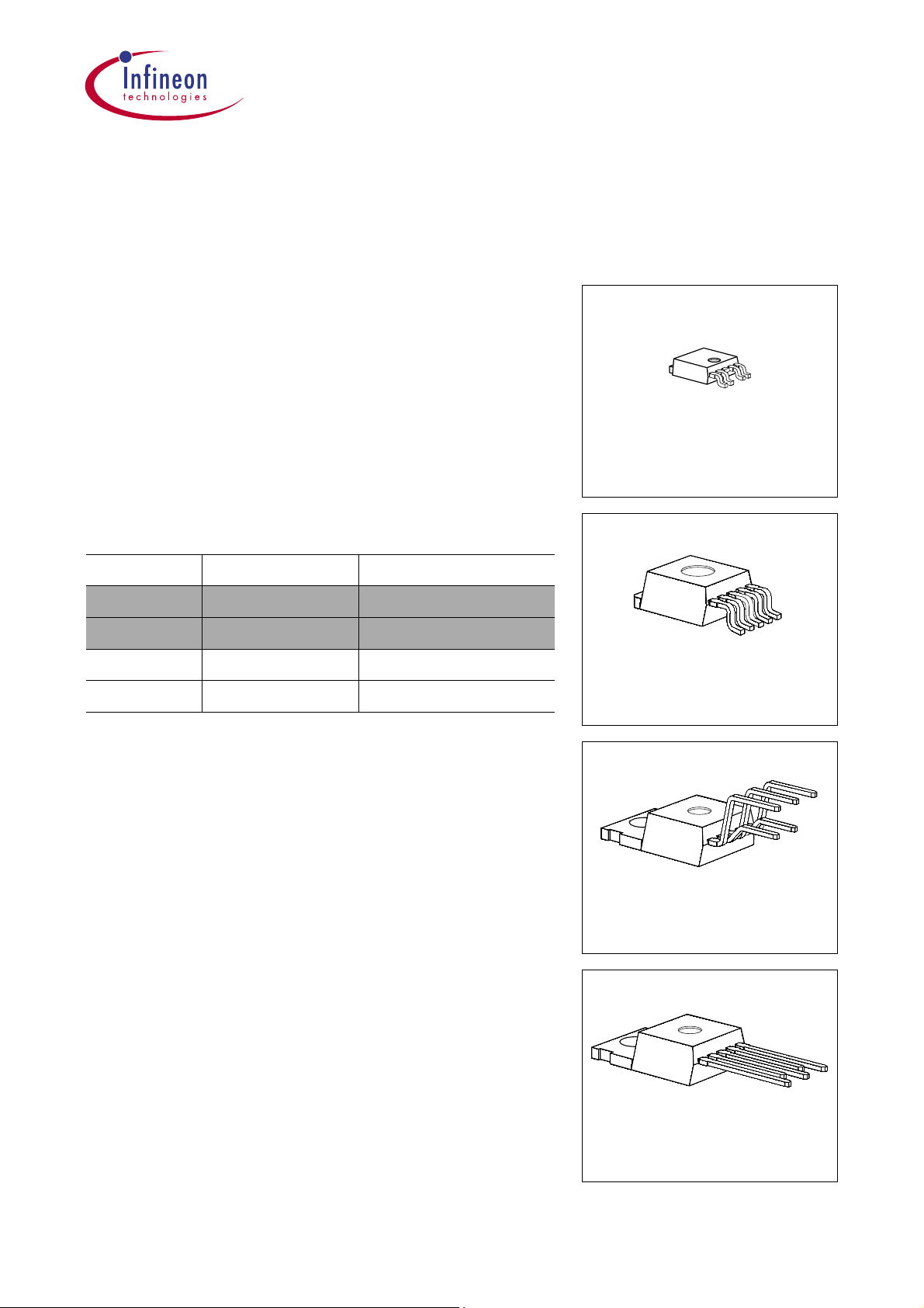
P-TO252-5-1
Type Ordering Code Package
TLE 4275 D Q67006-A9354 P-TO252-5-1 (SMD)
•
TLE 4275 G Q67006-A9343 P-TO263-5-1 (SMD)
•
• TLE 4275 Q67000-A9342 P-TO220-5-11
• TLE 4275 S Q67000-A9442 P-TO220-5-12
New type
•
Functional Description
The TLE 4275 is a monolithic integrated low-drop
voltage regulator in a 5 pin TO-package. An input
voltageupto45Visregulatedto
V
=5.0V.TheIC
Q,nom
is able to drive loads up to 450 mA and is short-circuit
proof. At overtemperature the TLE 4275 is turned off
by the incorporated tem perature protection. A reset
signal is generated for an outp ut voltage
V
Q,rt
4.65 V. The delay time can be pr ogrammed by the
external delay capacitor.
P-TO263-5-1
P-TO220-5-11
of typ.
P-TO220-5-12
Data Sheet Version 1.3 1 2001-04-24
Page 2

TLE 4275
Dimensioning Informat ion on External Components
C
The input capacitor
of approx. 1 Ω in series with
can be damped. The output capacitor
circuit. Stability is guaranteed at values CQ≥ 22 µF and an ESR of ≤ 5 Ω within the
operating temperature range.
Circuit Description
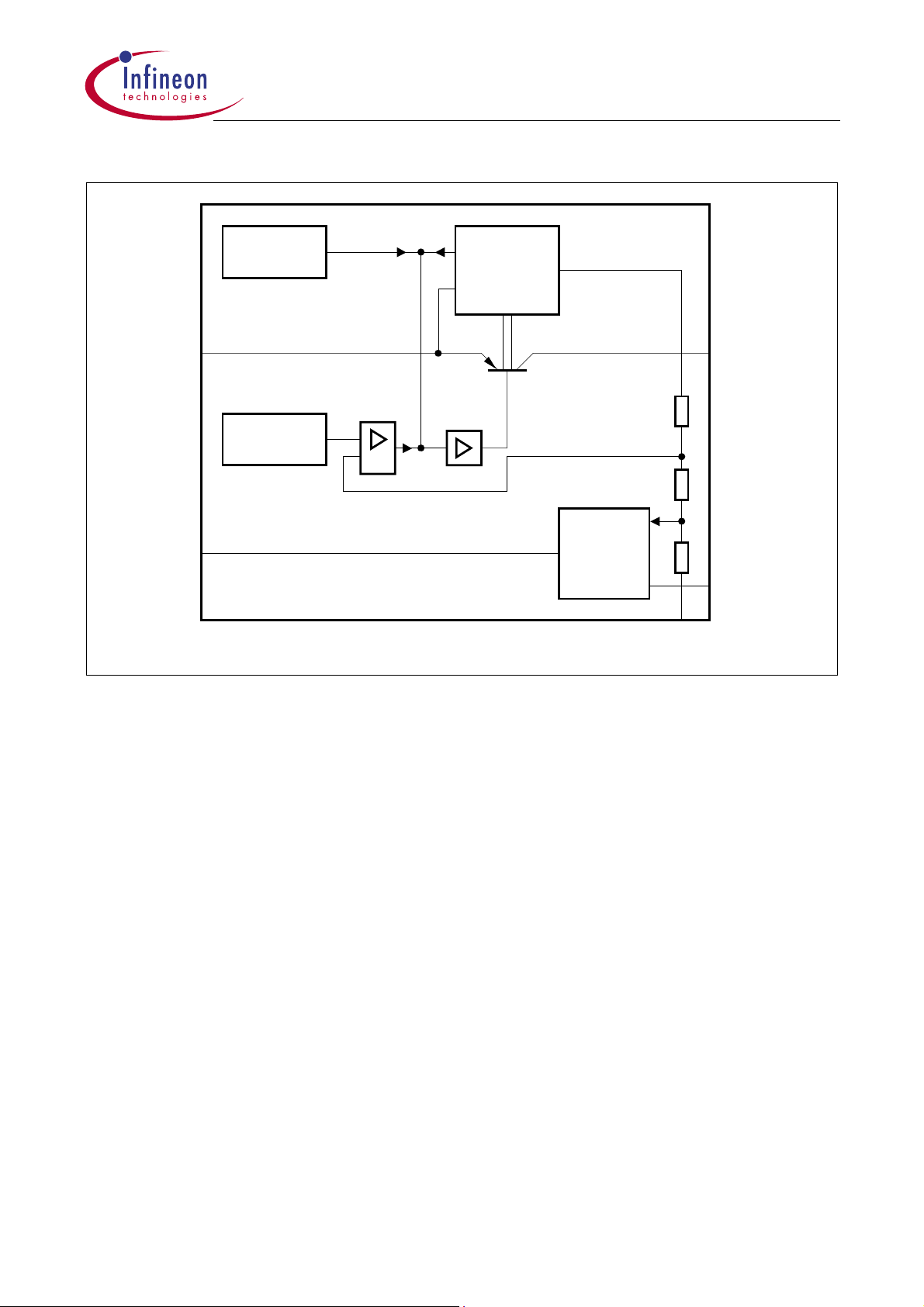
The controlamplifier compares a reference voltagetoavoltage that isproportional tothe
output voltage and drives the base of the series transistor via a buffer. Saturation control
as a function of the load c urrent prevents any oversaturat ion of the power element. The
IC also incorporates a number of internal circuits for protection against:
• Overload
• Over-temperature
• Reverse polarity
is necessa ry for compensation of line influences. Using a resistor
I
C
, the oscillating of input inductivity and input capacitance
I
C
is necessary for the stability of the regulation
Q
Data Sheet Version 1.3 2 2001-04-24
Page 3
TLE 4275
P-TO252-5-1 (D-PAK)
GND
15
ROΙ DQ
AEP02580
P-TO263-5-1 (SMD)
P-TO220-5-11
ΙROGNDDQ
IEP02527
P-TO220-5-12
GNDΙ
ROQD
AEP02756
Ι
GND
RO
Q
D
IEP02528
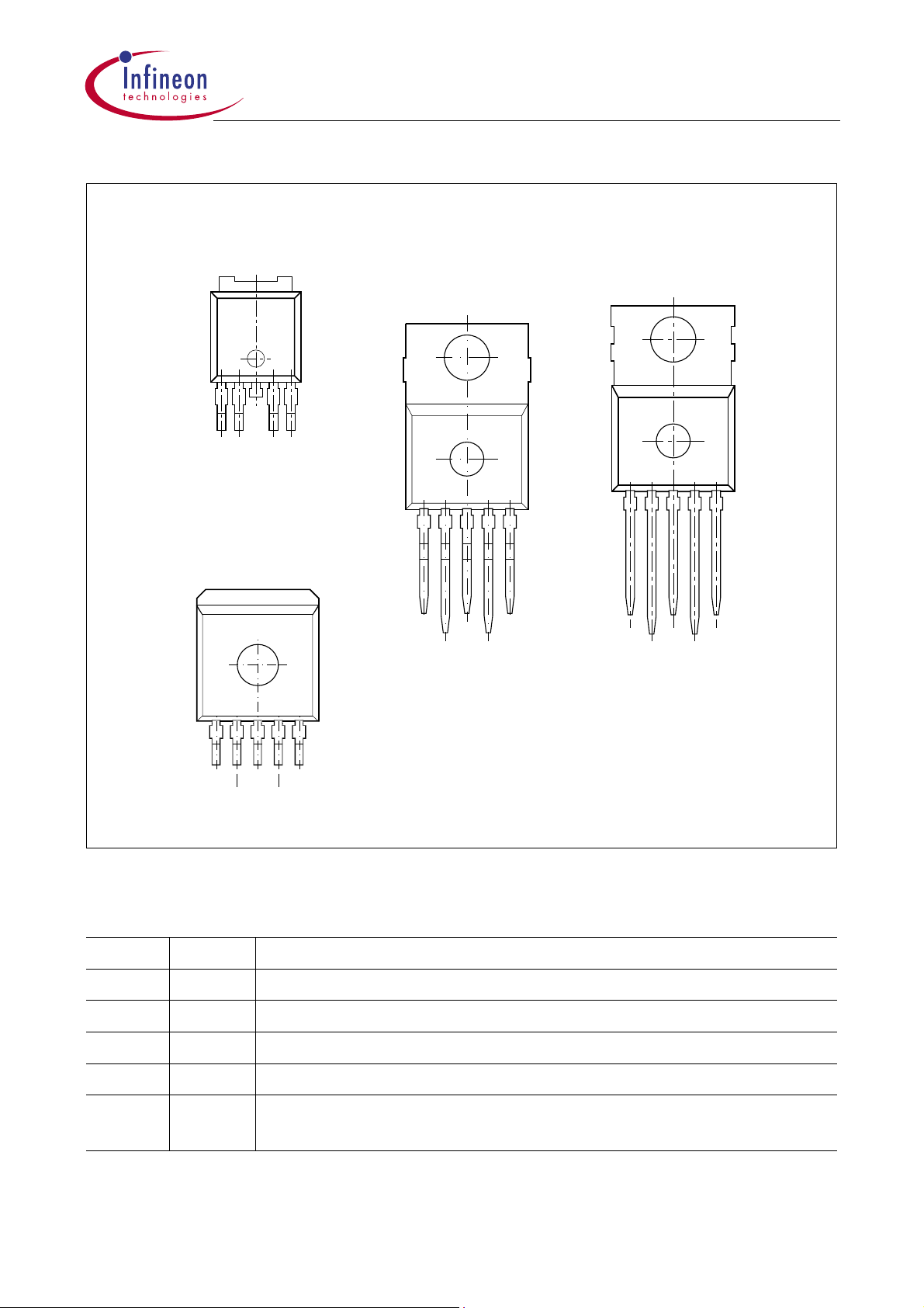
Figure 1 Pin Configuration (top view)
Pin Definitions and Functions
Pin No. Symbol Function
1 I Input; block to ground direct ly at the IC by a ceramic capacitor.
2ROReset O utput; open collector output
3GNDGround; Pin 3 internally connected to heatsink
4DReset Delay; connect capacitor to GND for setting delay time
5QOutput; block to ground with a ≥ 22 µF capacitor,
ESR < 5 Ω at 10 kHz.
Data Sheet Version 1.3 3 2001-04-24
Page 4
TLE 4275
Temperature
Sensor
1 5
I
Bandgap
Reference
4
D
Saturation
Control and
Protection
Circuit
Buffer
Reset
Generator
2
3
AEB02425
Q
RO
Figure 2 Block Diagram
Data Sheet Version 1.3 4 2001-04-24
Page 5
TLE 4275
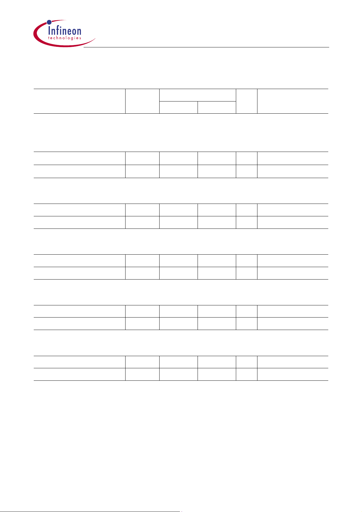
Absolute Maximum Ratings
Parameter Symbol Limit Values Unit Test Condition
min. max.
Voltage Regulator
Input
Voltage
Current
Output
Voltage
Current
Reset Ou tput
Voltage
Current
Reset D elay
Voltage
Current
V
I
V
I
V
I
V
I
I
Q
RO
D
I
Q
RO
D
–42 45
––
V
–
–
Internally limited
–1.0 16 V –
– – – Internally limited
–0.3 25 V –
–5 5 mA –
–0.3 7 V –
–2 2 mA –
Temperature
Junction temperature
Storage te mperature
T
j
T
stg
–40 150 °C–
–50 150 °C–
Note: Maximum ratings are absolute ratings; exceeding any one of these values may
cause irreversible damage to the integrated circuit.
Data Sheet Version 1.3 5 2001-04-24
Page 6
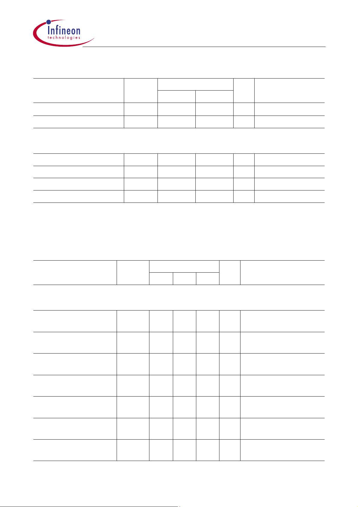
Operating Range
Parameter Symbol Limit Values Unit Remarks
min. max.
TLE 4275
Input voltage
Junction t emperature
V
T
I
j
5.5 42
V
–
–40 150 °C–
Thermal Resistance
Junction case
Junction ambient
Junction ambient R
Junction ambient R
1)Worstcase, regarding peaktemperature;zero airflow;mountedonaPCB FR4,80 × 80 × 1.5 mm
area 300 mm
2
R
R
thjc
thj-a
thj-a
thj-a
–4K/W –
–53K/W TO263
–78K/WTO252
–65K/W TO220
1)
1)
3
,heatsink
Characteristics
V
= 13.5 V; – 40 °C<Tj< 150 °C (unless otherwise specified)
I
Parameter Symbol Limit Values Unit Measuring Condition
min. typ. max.
Output
Output voltage
Output voltage
Output current
limitation
1)
Current consumption;
I
= II– I
q
Q
Current consumption;
I
= II– I
q
Q
Current consumption;
I
= II– I
q
Q
Current consumption;
I
= II– I
q
Q
V
V
I
I
I
I
I
Q
Q
Q
q
q
q
q
4.9 5.0 5.1
4.9 5.0 5.1
450 700 – mA –
– 150 200 µA IQ=1mA;
– 150 220 µA IQ=1mA;
–510mAIQ= 250 mA
–1222mAIQ= 400 mA
V
V
5mA<IQ<400mA
V
6V<
<28 V
I
5mA<IQ<200mA
V
6V<
T
=25°C
j
T
≤ 85 °C
j
<40V
I
Data Sheet Version 1.3 6 2001-04-24
Page 7
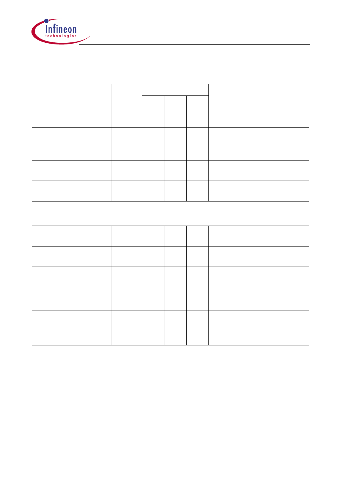
TLE 4275
Characteristics (cont’d)
V
=13.5V;–40°C<Tj< 150 °C (unless otherwise specified)
I
Parameter Symbol Limit Values Unit Measuring Condition
min. typ. max.
Drop voltage
1)
V
dr
– 250 500 mV IQ=300mA
V
= VI– V
dr
Q
Load regulation
Line regul ation
Power supply ripple
∆V
Q
∆V
Q
PSRR
rejection
Temperature output
voltage drift
dV
-----------
dT
Q
Reset Timing D and Output RO
Reset switching
V
Q,rt
threshold
Reset output low
V
ROL
voltage
Reset output lea kage
I
ROH
current
Reset charging current
I
D,c
– 1530mVIQ=5mAto400mA
–15 5 15 mV ∆Vl= 8 Vto32V
I
=5mA
Q
–60–dB fr= 100 Hz;
V
=0.5Vpp
r
–0.5–mV/K–
4.5 4.65 4.8 V–
–0.20.4VR
–010µA V
V
ext
Q
ROH
≥ 5kΩ;
>1V
=5V
3.0 5.5 9.0 µA VD=1V
Upper timing threshold
Lower timing threshold
Reset delay time
Reset reaction time
1)
Measured when the output voltage VQhas dropped 100 mV from the nominal value obtained at VI= 13.5 V.
Data Sheet Version 1.3 7 2001-04-24
V
V
t
t
DU
DRL
rd
rr
1.5 1.8 2.2 V –
0.2 0.4 0.7 V –
10 16 22 ms CD=47nF
–0.52µs CD=47nF
Page 8
I I
I
C
I
1
1000 µF
V
I
I
I
D, d
V
D
D, c
C
D
47 nF
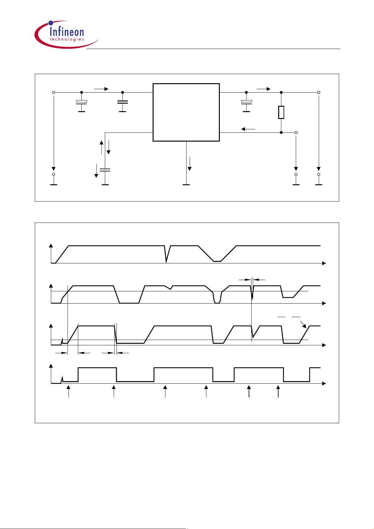
Figure 3 Test Circuit
C
I
2
100 nF
TLE 4275
I
RO
Q
C
Q
22 µF
R
5 k
ext
Ω
V
RO
AES02472
V
Q
I
1
D
4
3
Q
5
RO
2
GND
I
GND
V
Ι
t
<
V
Q
V
D
t
t
V
RO
Power-on-Reset Voltage Dip Secondary Overload
rd
Thermal
Shutdown
rr
Undervoltage
at Input
rr
V
d
dt
at OutputSpike
t
V
Q, rt
V
V
t
DU
DRL
Ι
D,c
=
C
D
t
t
AED03010
Figure 4 Reset Timing
Data Sheet Version 1.3 8 2001-04-24
Page 9
TLE 4275
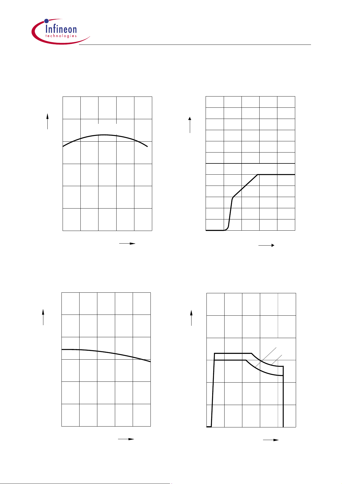
Output Voltage VQversus
Temperature
5.2
V
V
Q
5.1
5.0
4.9
4.8
4.7
4.6
-40 04080120 ˚C 160
T
j
V
= 13.5 V
I
AED03029
T
j
Output Voltage VQversus
Input Voltage
12
V
V
Q
10
8
6
4
2
0
0
V
I
R
= 25
L
2
4
68
AED01929
Ω
V
10
V
Ι
Output Current IQversus
Temperature
1200
mA
I
Q
1000
800
600
400
200
0
-40 04080120 ˚C 160
T
j
AED03034
T
j
Output Current IQversus
Input Voltage
1.2
A
I
Q
1.0
0.8
0.6
0.4
0.2
0
0 10 20 30 40 V50
V
I
T
AED03030
= 125 ˚C
j
25 ˚C
V
I
Data Sheet Version 1.3 9 2001-04-24
Page 10
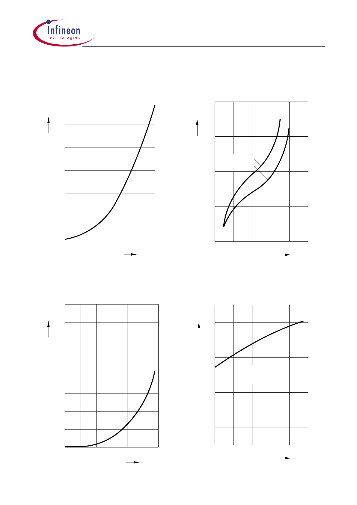
TLE 4275
Current Consumption I
versus Outp u t Current I
3
mA
Ι
q
2
V
= 13.5 V
Ι
1
0
20 40 60 80 120
0
q
Q
AED03084
Drop Voltage Vdrversus
Output Current
800
mV
V
dr
700
I
Q
AED03031
600
500
T
= 125 ˚C
j
25 ˚C
400
300
200
100
mA
Ι
Q
0
0
200 400 600 1000
mA
I
Q
Current Consumption I
versus Outp u t Current I
80
mA
Ι
q
70
60
50
40
30
V
= 13.5 V
Ι
20
10
0
100 200 300 400 600
0
q
Q
AED03085
Charge Current I
D,c
versus Temperature T
8
µA
I
D, c
7
I
D, c
j
AED03086
6
5
V
= 13.5 V
4
V
I
= 1 V
D
3
2
1
0
mA
Ι
-40
04080
120 160˚C
T
j
Data Sheet Version 1.3 10 2001-04-24
Page 11
TLE 4275
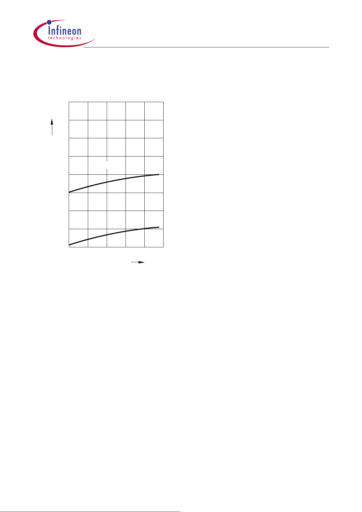
Delay Switching Threshold V
versus Tem perature T
4.0
DU
V
DRL
V
3.5
3.0
2.5
2.0
1.5
1.0
0.5
0
-40
V
04080 120 160
V
= 13.5 V
Ι
j
V
V
DU,VDRL
AED03083
DU
DRL
T
˚C
j
Data Sheet Version 1.3 11 2001-04-24
Page 12
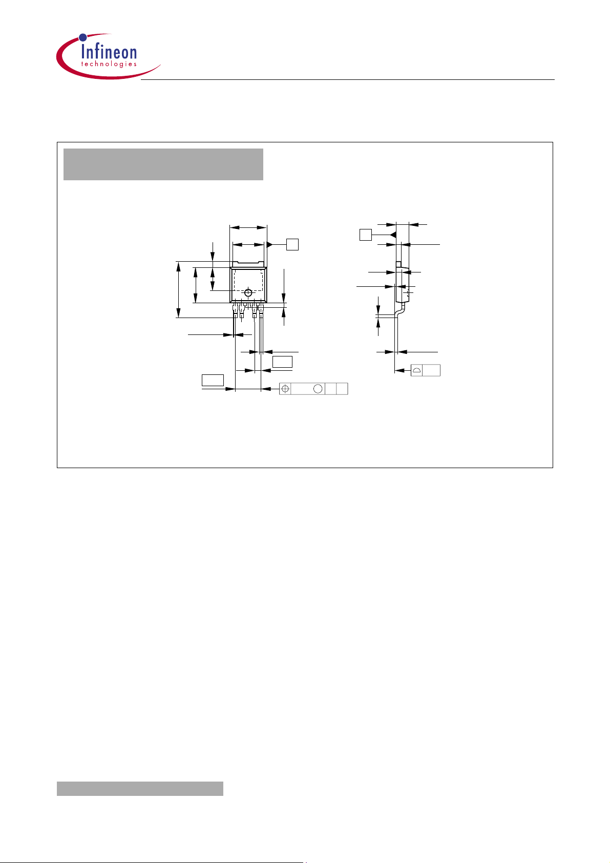
Package Outline s
P-TO252-5-1 (D-PAK)
(Plastic Transistor Single Outline)
TLE 4275
+0.15
6.5
-0.10
B
±0.1
1
0...0.15
0.51 min
-0.2
±0.5
6.22
9.9
0.15 max
per side
±0.1
1
(4.17)
5.4
±0.1
±0.15
0.8
5x0.6
A
±0.1
1.14
4.56
M
B
A0.25
All metal surfaces tin plated, except area of cut.
2.3
+0.05
-0.10
0.9
0.5
GPT09161
+0.08
-0.04
+0.08
-0.04
0.1
Sorts of Packing
Package outlines for tubes, trays etc. are contained i n our
Data Book “Package Information”.
SMD = Surface Mounted Device
Dimensions in mm
Data Sheet Version 1.3 12 2001-04-24
Page 13
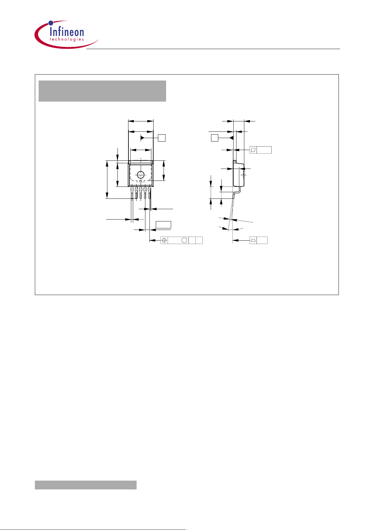
P-TO263-5-1 (SMD)
(Plastic Transistor Single Outline)
±0.2
10
±0.15
9.8
1)
8.5
±0.3
1
±0.2
9.25
(15)
5x0.8
±0.1
A
1)
7.55
0...0.15
4x1.7
TLE 4275
4.4
±0.1
1.27
B
0.1
2.4
±0.3
±0.5
2.7
4.7
0.5
8˚ max.
M
BA0.25
0.05
±0.1
0.1
1)
Typical
All metal surfaces tin plated, except area of cut.
GPT09113_malac
Sorts of Packing
Package outlines for tubes, trays etc. are contained i n our
Data Book “Package Information”.
SMD = Surface Mounted Device
Dimensions in mm
Data Sheet Version 1.3 13 2001-04-24
Page 14
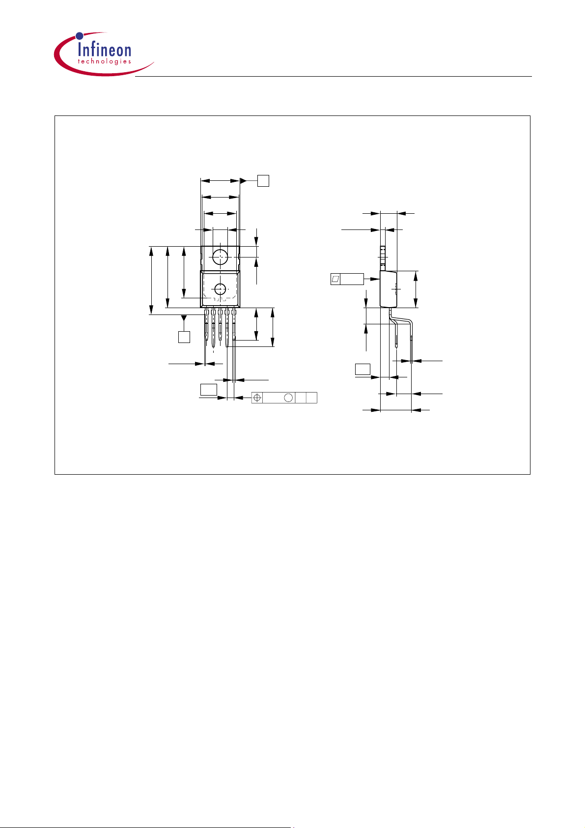
a
P-TO220-5-11
(Plastic Transistor Single Outline)
±0.2
10
±0.15
9.8
1)
8.5
3.7
-0.15
1)
±0.3
17±0.3
12.95
15.65
C
0...0.15
1.7
0.8
±0.2
2.8
±0.38.6
±0.1
TLE 4275
A
4.4
±0.1
1.27
10.2±0.3
0.05
3.7±0.3
2.4
M
A0.25
C
8.4
±0.4
±0.2
9.25
0.5
3.9
±0.1
±0.4
1)
Typical
All metal surfaces tin plated, except area of cut.
gpt09064_m
Sorts of Packing
Package outlines for tubes, trays etc. are contained i n our
Data Book “Package Information”.
Dimensions in mm
Data Sheet Version 1.3 14 2001-04-24
Page 15
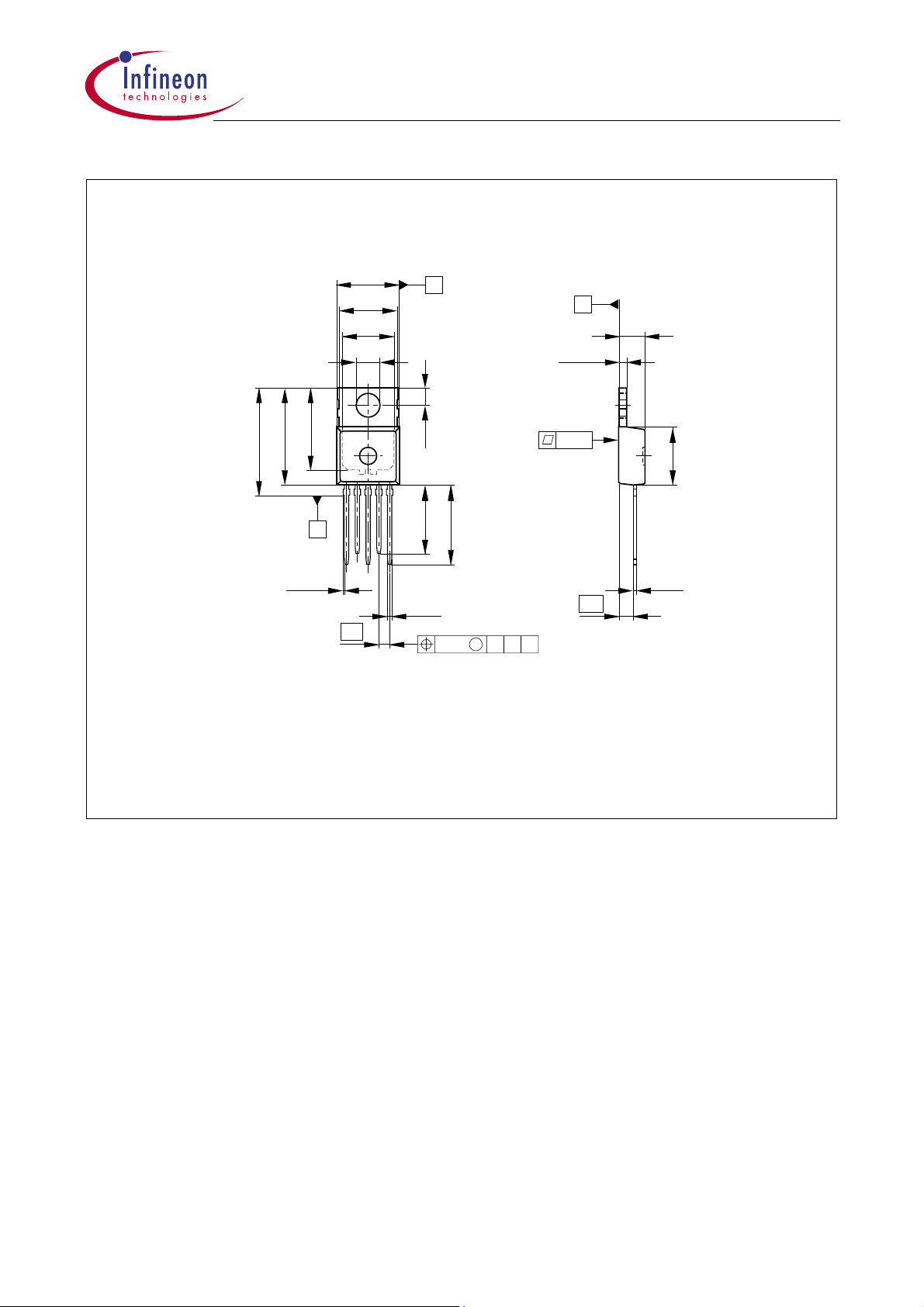
P-TO220-5-12
(Plastic Transistor Single Outline)
±0.2
10
±0.15
9.8
1)
8.5
3.7
-0.15
1)
±0.3
±0.3
17
12.95
15.65
C
A
±0.2
2.8
±0.5
11
±0.5
13
1.27
0.05
TLE 4275
B
4.4
±0.1
±0.2
9.25
0...0.15
1.7
6x
0.8
±0.1
2.4
M
BA0.25
C
Typical
1)
All metal surfaces tin plated, except area of cut.
±0.1
0.5
gpt09065_mal
Sorts of Packing
Package outlines for tubes, trays etc. are contained i n our
Data Book “Package Information”.
Dimensions in mm
Data Sheet Version 1.3 15 2001-04-24
Page 16

Edition 2001-04-24
Published by
Infineon Technologies AG i. Gr.,
St.-Martin-Strasse 53
D-81541 München
©
Infineon Technologies AG 1999
All Rights Reserved.
Attention please!
The information herein is given to describe
certain components and shall not be considered as warranted characteristics.
Terms of delivery and rights to technical
change reserved.
We hereby disclaim any and all warranties,
including but not limited to warranties of noninfringement, regarding circuits, descriptions
and charts stated herein.
Infineon Technologiesis an approvedCECC
manufacturer.
TLE 4275
Information
For further information on technology, delivery terms and conditions and prices please
contactyour nearest Infineon Technologies
Officein Germany or our Infineon Technologies Representatives worldwide(see address list).
Warnings
Due to technicalrequirements components
may contain dangerous substances. For informationonthetypesinquestionplease
contactyour nearest Infineon Technologies
Office.
InfineonTechnologiesComponentsmayonly
be used in life-support devices or systems
with the express written approval of Infineon
Technologies,if a failureof such components
can reasonablybe expected to causethe failureof thatlife-supportdevice or system,or to
affect the safety or effectiveness of that device or system. Life support devices or systems are intended to be implanted in the human body, or to support and/or maintain and
sustainand/orprotecthumanlife.Iftheyfail,it
is reasonable toassume that the health of the
user or other persons may be endangered.
Data Sheet Version 1.3 16 2001-04-24
 Loading...