

Page 1
现货库存、技术资料、百科信息、热点资讯,精彩尽在鼎好!
TLE 4269
5-V Low-Drop Fixed Voltage Regulator
Features
● Output voltage tolerance ≤ ± 2 %
● Very low current consumption
● Early warning
● Reset output low doown to V
● Overtemperature protection
● Reverse polarity proof
● Settable reset threshold
● Very low drop voltage
● Wide temperature range
● Integrated pull up resistor at logic outputs
Type Ordering Code Package
= 1 V
Q
TLE 4269
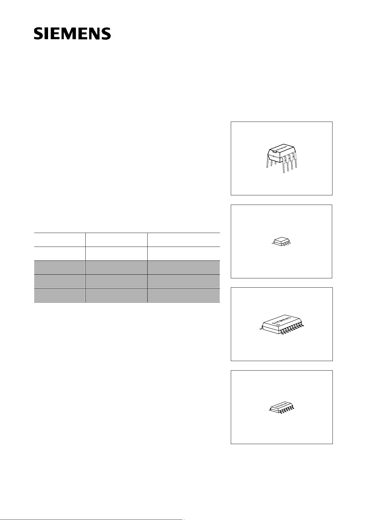
P-DIP-8-4
TLE 4269 A Q67000-A9190 P-DIP-8-4
TLE 4269 G Q67006-A9173 P-DSO-8-1 (SMD)
TLE 4269 GM Q67006-A9288 P-DSO-14-4 (SMD)
▼
TLE 4269 GL Q67006-A9192 P-DSO-20-6 (SMD)
▼ New type
Functional Description
This device is a voltage regulator with a fixed 5-V
output, e.g. in a P-DSO-8-1 package. The maximum
operating voltage is 45 V. The output is able to drive a
150 mA load. It is short circuit protected and the
thermal shutdown switches the output off if the junction
temperature is in excess of 150 °C. A reset signal is
V
generated for an output voltage of
<4.6V. The
Q
reset threshold voltage can be decreased by external
connection of a voltage divider. The reset delay time
can be set by an external capacitor. R eset and sense
output have integrated pull up resistors. If the
integrated resistors are not desired TLE 4279 can be
used. It is also possi ble to supervise the input voltage
by using an integrated comparator to give a low voltage
warning.
P-DSO-8-1
P-DSO-20-6
P-DSO-14-4
Semiconductor Group 1 1998-11-01
Page 2
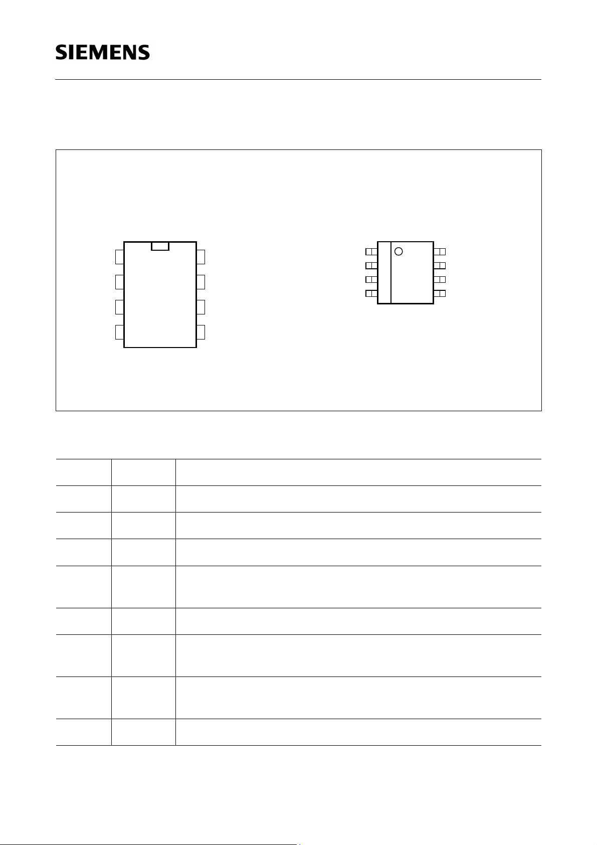
Pin Configuration
(top view)
TLE 4269
P-DIP-8-4
P-DSO-8-1
18
Ι Q
S
RE
Ι
AEP01813
SO72
R63
GNDD54
Ι
2
ΙS
RE
3
D5
4
8
7
6
AEP01668
Q
SO
R
GND
1
Pin Definitions and Functions (TLE 4269 A and TLE 4269 G)
Pin No. Symbol Function
1 I Input; block directly to GND on the IC with a ceramic capacitor.
2SISense Input; if not needed connect to Q.
3REReset Threshold; if not needed connect to ground.
4DReset Delay; to select delay time, connect to GND via external
capacitor.
5GNDGround
6RReset Output; the open-collector output is internally linked to Q
via a 20 kΩ pull-up resistor.
7SOSense Output; the open-collector output is internally linked to the
output via a 20 kΩ pull-up resistor.
8Q5-V Output; connect to GND with a 10 µF capacitor, ESR < 10 Ω.
Semiconductor Group 2 1998-11-01
Page 3
Pin Configuration
(top view)
TLE 4269
P-DSO-14-4
RE
GND
GND
GND GND
GND
1
2
D
3
4
5
6
7SO
R
14
13
12
11
10
9
8
AEP02248
SI
Ι
GND
GND
Q
Pin Definitions and Functions (TLE 4269 GM)
Pin No. Symbol Function
1REReset Threshold; if not needed connect to GND.
2DReset Delay; connect to GND via external delay capacitor for
setting delay time.
3, 4, 5, 6 GND Ground
7RReset Output; open-collector output, internally connected to Q
via a pull-up resistor of 20 kΩ.
8SOSense Output; open-collector output, internally connected to Q
via a 20 kΩ pull-up resistor.
9Q5-V Output; connect to GND with a 10 µF capacitor, ESR < 10 Ω.
10, 11, 12 GND Ground
13 I Input; block to GND directly at the IC by a ceramic capacitor.
14 SI Sense Input; if not needed connect to Q.
Semiconductor Group 3 1998-11-01
Page 4
Pin Configuration
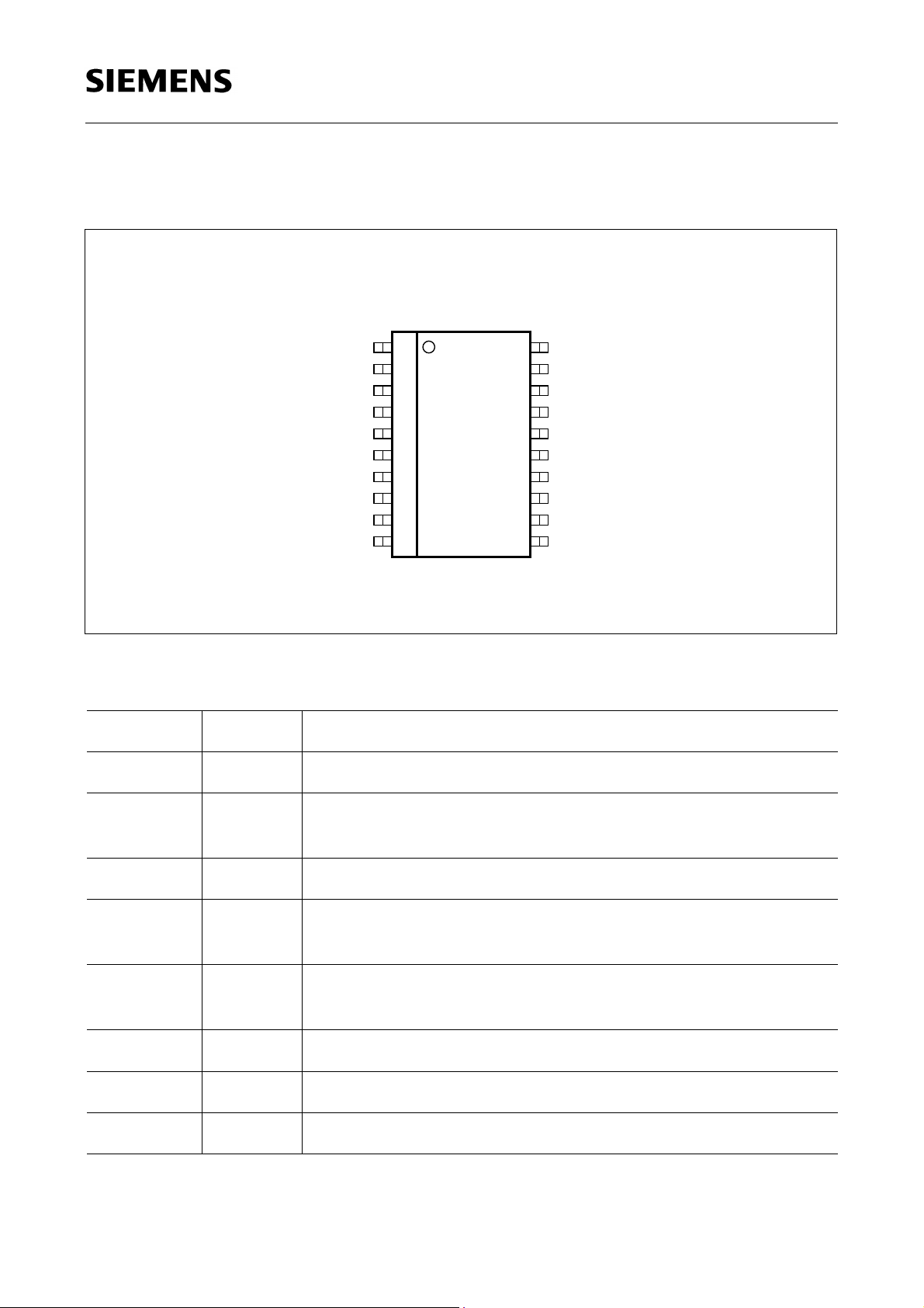
(top view)
TLE 4269
P-DSO-20-6
RE
D
N.C.
GND
GND
GND
GND
N.C.
N.C.
R
1
2
3
4
5
6
7
8
9
10
20
19
18
17
16
15
14
13
12
11
AEP01802
Ι
S
Ι
N.C.
GND
GND
GND
GND
N.C.
Q
SO
Pin Definitions and Functions (TLE 4269 GL)
Pin No. Symbol Function
1REReset Threshold; if not needed connect to GND.
2DReset Delay; to select delay time connect to GND via external
capacitor.
4-7, 14-17 GND Ground
10 R Reset Output; the open-collector output is internally linked to
Q via 20 kΩ pull-up resistor.
11 SO Sense Output; the open-collector output is internally linked to
Q via 20 kΩ pull-up resistor.
12 Q Output; connect to GND with a 10 µF capacitor, ESR < 10 Ω.
19 I Input; block directly to GND at the IC by a ceramic capacitor.
20 SI Sense Input; if not needed connect to Q.
Semiconductor Group 4 1998-11-01
Page 5

TLE 4269
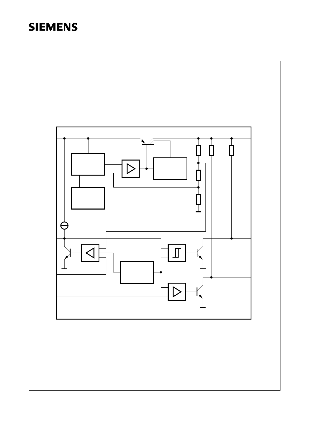
Circuit Description
The control amplifier compares a reference voltage, made highly accurate by resistance
balancing, with a voltage propo rtional to the output voltage and drives the base of the
series PNP transistor via a buffe r. Saturation control as a function of the load current
prevents any over-saturation of the power element.
In the reset generator block a comparator compares a reference voltage independent of
the input voltage with the scaled-down output voltage. If the output voltage reaches 4.6 V
the reset delay capaci tor is discharged and the reset output is set to low . This low is
guaranteed down to an output voltage of 1 V. As the output voltage incr eases again,
from 4.6 V onward the reset delay capacitor is charged with constant current. When the
V
capacitor voltage reaches the upper switching threshold
choosing the value of this capaci tor, the reset delay time can be selected over a wide
range. With the reset t hresh old in put RE it is possible to lo we r the res et threshold
pin RE is connected to pin Q vi a a voltage divider, for example, the re set condition is
reached when this voltage is decreased below the switching threshold
, the reset returns to high. By
dT
V
V
of 1.35 V.
re
rt
. If
Another comparator compares the signal of the pin SI, normally fed by a voltage divider
from the input voltage, with the reference and gives an early warning on the pin SO. It is
also possible to superwise an other voltage e.g. of a second regulator, or to build a
watchdog circuit with few external components.
Application Description
C
The input capacitor
approx. 1 Ω in series with
capacita nce c an be damp ed. Th e out put ca pacit or C
is necessary for compensating line influences. Using a resistor of
I
C
, the oscillating circuit consisting of input inductivity and input
I
is necessary for the stability of the
Q
regulating circuit. Stability is guaranteed at values ≥ 10 µF and an ESR ≤ 10 Ω within the
operating temperature rang e. For small tol erances of the rese t delay the s pread of the
capacitance of the delay capacitor and its temperature coefficient should be noted.
Semiconductor Group 5 1998-11-01
Page 6
TLE 4269
D
RE
Ι
Error
20 kΩΩk20
Q
Amplifier
Reference
Current and
Saturation
Control
Trimming
R
Reference
SO
SI
AEB01669
Block Diagram
Semiconductor Group 6 1998-11-01
Page 7

Absolute Maximum Ratings
T
= – 40 to 150 °C
j
Parameter Symbol Limit Values Unit Notes
min. max.
Input
TLE 4269
Input voltage
Input current
Sense Input
Input voltage
Input current
Reset Threshold
Voltage
Current
Reset Delay
Voltage
V
I
V
I
V
I
V
I
SI
RE
I
SI
RE
D
– 40 45 V –
– – – internal limited
– 0.3 45 V –
11mA–
– 0.3 7 V –
– 10 10 mA –
– 0.3 7 V –
Current
I
D
– – – internal limited
Ground
Current
I
GND
50 – mA –
Reset Output
Voltage
Current
Semiconductor Group 7 1998-11-01
V
I
R
R
– 0.3 7 V –
– – – internal limited
Page 8

Absolute Maximum Ratings (cont’d)
T
= – 40 to 150 °C
j
Parameter Symbol Limit Values Unit Notes
min. max.
Sense Output
TLE 4269
Voltage
Current
5-V Output
Output voltage
Output current
Temperature
Junction temperature
Storage temperature
Operating Range
Input voltage
Junction temperature
V
I
V
I
T
T
V
T
SO
Q
SO
Q
j
Stg
I
j
– 0.3 7 V –
– – – internal limited
– 0.3 7 V –
–5 – mA –
– 150 °C–
– 50 150 °C –
–45V –
– 40 150 °C –
Thermal Data
Junction-ambient
Semiconductor Group 8 1998-11-01
R
R
thja
thjc
– 100
200
70
70
–60
60
30
30
K/W
K/W
K/W
K/W
K/W
K/W
K/W
K/W
P-DIP-8-4
P-DSO-8-1
P-DSO-14-4
P-DSO-20-6
P-DIP-8-4
P-DSO-8-1
P-DSO-14-4
P-DSO-20-6
Page 9
TLE 4269
Characteristics
V
=13.5V; Tj= – 40 °C<Tj< 125 °C
I
Parameter Symbol Limit Values Unit Measuring
Condition
min. typ. max.
Output voltage
Current limit
Current consumption;
I
= I
– I
q
I
Q
Current consumption;
I
= I
– I
q
I
Q
Current consumption;
I
= I
– I
q
I
Q
Drop voltage
V
I
I
I
I
V
Q
q
q
q
Load regulation ∆V
Line regulation ∆
V
Reset Generator
Q
4.90 5.00 5.10 V 1 mA ≤ IQ≤ 100 mA
V
6V≤
≤ 16 V
I
150 200 500 mA –
– 150 300 µA IQ≤ 1mA,Tj<85°C
– 250 700 µA IQ=10mA
–28 mAIQ=50mA
dr
Q
Q
–0.250.5VIQ= 100 mA
–1030mVIQ= 5 mA to 100 mA
–1040mVVI= 6 V to 26 V
I
=1mA
Q
1)
Switching threshold
V
rt
4.50 4.60 4.80 V –
Reset pull up – 10 20 40 kΩ –
Reset low voltage
Delay switching
V
V
R
dt
–0.10.4VR
1.4 1.8 2.2 V –
intern
threshold
Switching threshold
Reset delay low voltage
Charge current I
1)
Drop voltage = VI– VQ (measured when the output voltage has dropped 100 mV from the
nominal value obtained at 13.5 V input.)
Semiconductor Group 9 1998-11-01
V
V
st
D
d
0.3 0.45 0.60 V –
–0.1VVQ< V
RT
3.0 6.5 9.5 µA VD=1V
Page 10

TLE 4269
Characteristics (cont’d)
V
= 13.5 V; Tj= – 40 °C<Tj< 125 °C
I
Parameter Symbol Limit Values Unit Measuring
Condition
min. typ. max.
Delay time L → H
Delay time H → L
Switching voltage
t
t
V
d
t
re
17 28 –msCD=100nF
–1– µs CD=100nF
1.26 1.35 1.44 V VQ>3.5V
Input Voltage Sense
Sense threshold high
Sense threshold low
Sense output
V
si, high
V
si, low
V
SO, low
1.24 1.31 1.38 V –
1.16 1.20 1.28 V –
–0.10.4VVSI<1.20V;
low voltage
Sense pull up – 10 20 40 kΩ –
Sense input current
I
SI
– 10.11 µA –
V
R
i
intern
>3V
Semiconductor Group 10 1998-11-01
Page 11

TLE 4269
Ι
Ι
C
1000 Fµ
V
Ι Q
Ι
470 nF
1
Ι
ΙS
23
4567
V
SΙ
C
D
100 nF
Measuring Circuit (P-DIP-8-4/P-DSO-8-1)
V
Ι
TLE 4269
Ι
Ι
D
GND
V
D
Ι
Q
8
C
Q
22 Fµ
Ι
RE
V
V
R
SO
V
RE
V
AES01670
t
<
V
RT
V
Q
V
D
t
d
V
RO
Power-on-Reset Voltage Dip Secondary Overload
Thermal
Shutdown
t
RR
Undervoltage
at Input
Reset Timing Diagram
RR
Ι
V
d
d
=
dt
C
D
at OutputSpike
V
DT
V
ST
AED01542
Semiconductor Group 11 1998-11-01
Page 12

Sense
Input
Voltage
V
SI, High
V
SI, Low
Sense
Output
TLE 4269
t
High
Low
Sence Timing Diagram
t
AED02559
Semiconductor Group 12 1998-11-01
Page 13

TLE 4269
Charge Current Id versus
T
Temperature
16
Aµ
Ι
d
14
12
10
8
6
4
2
0
-40
j
V
= 13.5 V
Ι
1.0 V=
V
C
04080120 C 160
AED01803
T
j
Switching Voltage V
T
Temperature
j
3.2
V
V
D
2.8
2.4
2.0
1.6
1.2
0.8
0.4
0
-40
04080120 C 160
and V
dt
V
= 13.5 V
Ι
V
dt
V
st
versus
st
AED01804
T
j
Drop Voltage
V
Output Current
500
V
dr
mV
400
300
T
200
100
0
0
30 60 90 120 180mA
versus
dr
I
Q
j
T
C125=
=25C
j
AED01805
Ι
Q
Reset Switching Threshold
versus Temperature Tj
1.7
V
V
re
1.6
1.5
1.4
1.3
1.2
1.1
1.0
0.9
-40
04080120 C 160
V
re
AED01806
T
j
Semiconductor Group 13 1998-11-01
Page 14

TLE 4269
Current Consumption IQ versus
V
Input Voltage
30
Ι
q
mA
25
20
15
10
5
0
0
I
Ω
33=
R
L
R
=50
Ω
L
Ω
100=
R
L
= 200
R
L
10 20 30 40
AED01807
Ω
V50
V
Ι
Output Voltage
Input Voltage
12
V
Q
V
10
8
6
4
2
0
0
V
246
V
versus
Q
I
R
=50
L
AED01808
Ω
8 V10
V
Ι
Sense Threshold
V
si
versus Temperature Tj
1.6
V
si
V
V
= 13.5 V
1.5
1.4
1.3
1.2
1.1
1.0
-40 04080120 C 160
Ι
Sense Output High
Sense Output Low
AED01809
T
j
Output Voltage
Temperature
5.2
V
Q
V
5.1
5.0
4.9
4.8
4.7
4.6
-40
T
04080
V
j
Q
versus
V
= 13.5 V
Ι
AED01671
120 C 160
T
j
Semiconductor Group 14 1998-11-01
Page 15

TLE 4269
Output Current IQ versus
V
Input Voltage
350
Ι
mA
Q
300
250
200
150
100
50
0
0
I
=25C
T
j
T
10 20 30
C125=
j
AED01810
40 V50
V
Ι
Current Consumption
I
Output Current
12
Ι
q
mA
10
8
6
4
2
0
0
20 40 60 80 120mA
Q
V
T
13.5 V=
Ι
=25 C
j
I
versus
q
AED01811
Ι
Q
Current Consumption
I
10
Q
13.5 V=
V
Ι
=25 C
T
j
20 30 40 50
Output Current
1.6
mA
Ι
q
1.4
1.2
1.0
0.8
0.6
0.4
0.2
0
0
I
versus
q
AED01812
mA
Ι
Q
Semiconductor Group 15 1998-11-01
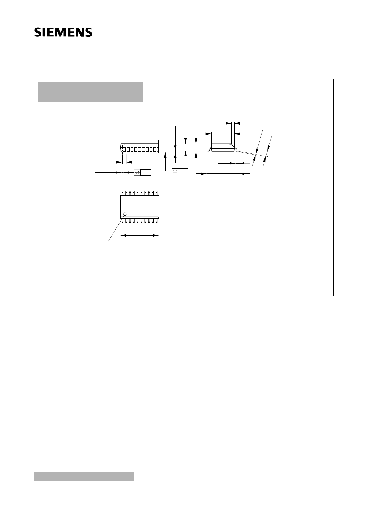
Page 16

Package Outlines
P-DIP-8-4
(Plastic Dual In-line)
TLE 4269
Sorts of Packing
Package outlines for tubes, trays etc. are contained in our
Data Book “Package Information”
GPD05583
Dimensions in mm
Semiconductor Group 16 1998-11-01
Page 17

P-DSO-14-4 (SMD)
(Plastic Dual Small Outline)
-0.1
0.2
-0.2
1.45
4
-0.2
1.75 max
TLE 4269
0.35 x 45˚
1)
+0.06
0.19
0.35
1.27
+0.15
2)
0.1
0.2 14x
±0.2
6
0.4
+0.8
8˚ max.
14 8
17
8.75
-0.2
1)
Index Marking
1) Does not include plastic or metal protrusion of 0.15 max. per side
2) Does not include dambar protrusion of 0.05 max. per side
GPS05093
Sorts of Packing
Package outlines for tubes, trays etc. are contained in our
Data Book “Package Information”
Dimensions in mm
SMD = Surface Mounted Device
Semiconductor Group 17 1998-11-01
Page 18

P-DSO-8-1 (SMD)
(Plastic Dual Small Outline)
TLE 4269
Sorts of Packing
Package outlines for tubes, trays etc. are contained in our
Data Book “Package Information”
SMD = Surface Mounted Device
GPS05121
Dimensions in mm
Semiconductor Group 18 1998-11-01
Page 19
P-DSO-20-6 (SMD)
(Plastic Dual Small Outline)
1.27
+0.15
0.35
2)
0.2 24x
1120
-0.1
0.2
-0.2
2.45
0.1
7.6
2.65 max
10.3
0.35 x 45˚
1)
-0.2
+0.8
0.4
±0.3
+0.09
0.23
TLE 4269
8˚ max
GPS05094
110
12.8
-0.2
1)
Index Marking
1) Does not include plastic or metal protrusions of 0.15 max per side
2) Does not include dambar protrusion of 0.05 max per side
Sorts of Packing
Package outlines for tubes, trays etc. are contained in our
Data Book “Package Information”
Dimensions in mm
SMD = Surface Mounted Device
Semiconductor Group 19 1998-11-01
 Loading...