

Power Factor Controller
IC for High Power Factor and
Active Harmonic Filter
Features
● IC for sinusoidal line-current consumption
● Power factor approaching 1
● Controls boost converter as an active harmonics filter
● Direct drive of SIPMOS transistor
● Zero crossing detector for discontinuous operation mode
with variable frequency
● 110/220 V AC operation without switchover
● Standby current consumption of 0.5 mA
● Start/stop monitoring circuit for lamp generators
TDA 4814
Bipolar IC
P-DIP-14-1
Type Ordering Code Package
TDA 4814 A Q67000-A8163 P-DIP-14-1
■
■ Not for new design
Semiconductor Group 1 01.96
TDA 4814 A
TDA 4814
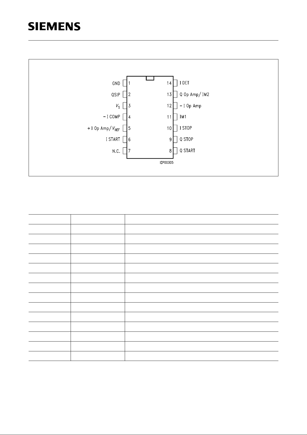
Pin Configurations
(top view)
Pin Definitions and Functions
Pin Symbol Function
1 GND Ground
2 QSIP Driver output
3
V
S
Supply voltage
4–ICOMP Negative comparator input
5+I Op Amp/V
REF
Positive input/reference voltage
6 I START Start input
7 N.C. Not connected
8 Q START Start output
9 Q STOP Stop output
10 I STOP Stop input
11 I M1 Multiplier input M1
12 – I Op Amp Negative input Op amplifier
13 QOp Amp/I M2 Op amplifier output and multiplier input M2
14 I DET Detector input
Semiconductor Group 2
TDA 4814
The TDA 4814 A contains all functions for designing electronic ballasts and switched-mode power
supplies with sinusoidal line current consumption and a power factor approaching 1.
They control a boost converter as an active harmonic filter in a discontinuous (triangular shaped
current) mode with variable frequency.
The output voltage of this filter is regulated with high efficiency. Therefore the device can easily be
operated on different line voltages (110/220 VAC) without any switchover.
The on-chip start/stop circuit monitors the lamp generator of electronic ballasts. It starts a selfoscillating lamp generator and shuts it down in the event of malfunction, e.g. if the lamp is defective.
A typical application is in electronic ballasts, especially when a large number of such lamps are
concentrated on one line supply point.
Besides that a separate driver ground (GND QSIP) is implemented.
The TDA 4814 A in a P-DIP-14-1 package.
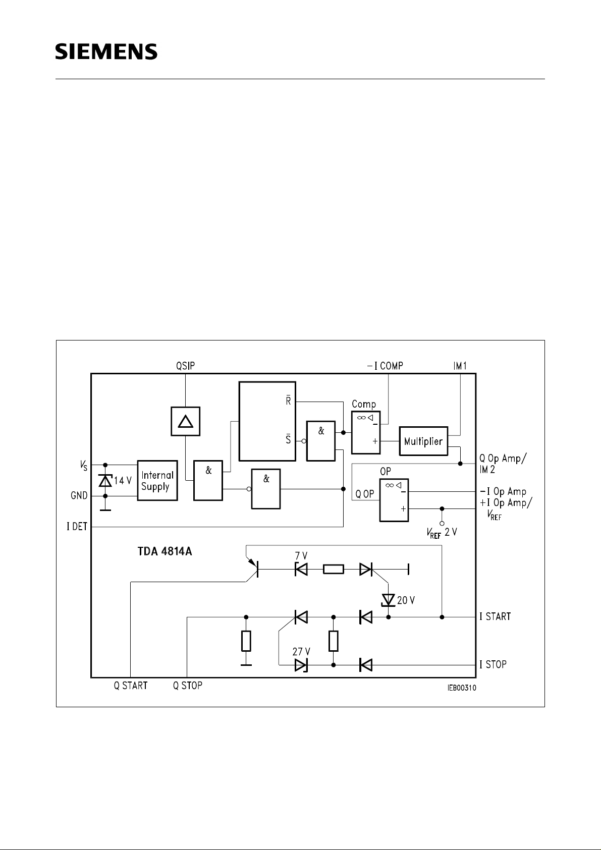
Block Diagram
Semiconductor Group 3

TDA 4814
Circuit Description
This device has a conditioning circuit for the internal power supply. It allows standby operation with
very low current consumption (less than 0.5 mA), a hysteresis between enable and switch-off levels
and an internal voltage stabilization. An integrated Z-diode limits the voltage on VS, when
impressed current is fed.
The output driver (Q SIP) is controlled by detector input and current comparator.
The detector input (I DET) which is highly resistive in the operating state reacts on hysteresis-
determined voltage levels. To keep down the amount of circuitry required, clamping diodes are
provided which allow control by a current source.
The operating state of the boost converter choke is sensed via the detector input. H-level means
that the choke discharges and the output driver is inhibited. H-level sets a flip-flop, which stores the
switch-off instruction of the current comparator to reduce susceptibility to interference. As soon as
demagnetization is finished the choke voltage reverses and the detector input is set to L-level, thus
enabling the output driver. This ensures that the choke is always currentless when the SIPMOS
transistor switches on and that no current gaps appear.
The nominal voltage of the multiplier output is compared to the voltage derived from the actual line
current (–I COMP), thus setting the switch-off threshold of the comparator. The current comparator
blocks the output driver when the nominal peak value of the choke current given by the multiplier
output is reached.
This state is maintained in the flip-flop until H-level appears at detector input which takes over the
hold function and resets the flip-flop.
Operating states might occur without any useful detector signal. This is the case with magnetic
saturation of the choke and when the input voltage approaches or exceeds the output voltage as,
for example, during switch-on. The driver remains inhibited for the flip-flop due to the absent set
signal.
The trigger signal can be derived from the subsequent lamp generator, a SMPS control device or,
if neither one of them is available, from the start circuit designed as a pulse generator in the
TDA 4814. The trigger signal level should be so low that with standard operation the signal from the
detector winding dominates.
The multiplier delivers the preset nominal value for the current comparator by multiplying the input
voltage, which determines the nominal waveform (IM1) and the output voltage of the control
amplifier.
The control amplifier stabilizes the output dc voltage of the active harmonic filter in the event of load
and input voltage changes. The control amplifier compares the actual output voltage to a
reference voltage which is provided in the IC and stable with temperature.
Semiconductor Group 4

TDA 4814
Output Driver
The output driver is intended to drive a SIPMOS transistor directly. It is designed as a push-pull
stage.
Both the capacitive input impedance and keeping the gate level at zero potential in standby
operation by an internal 10-kΩ-resistor are taken into account. Possible effects on the output driver
by line inductances or capacitive couplings via SIPMOS transistor Miller capacitance are limited by
diodes connected to ground and supply voltage.
Ground Pins
Between the ground pins GND and GND QSIP, a very close and low-impedance connection is to
be established.
Monitoring Circuit (I START, I STOP, Q START, Q STOP)
The monitoring circuit guarantees the secure operation of subsequent circuitries.
Any circuitry that is shut down because of a fault, for instance, cannot be started up again until the
monitoring start (I START / Q START) has turned on and a positive voltage pulse has been
impressed on Q START. This function starts for example the lamp generator of an electronic ballast
or generates auxiliary trigger signals for the detector input.
If there is a defect present (e.g. defective fluorescent lamp) the monitoring stop (I STOP /
Q STOP) will shut down either the entire unit or simply the circuitry that has to be protected. No
restart is possible then until the hold current impressed on I START or Q STOP has been
interrupted (e.g. by a power down).
Semiconductor Group 5
 Loading...