

Siemens TDA4700A, TDA4718A Datasheet
Control IC for Single-Ended and Push-Pull
Switched-Mode Power Supplies (SMPS)
Features
● Feed-forward control (line hum suppression)
● Symmetry inputs for push-pull converter
(TDA 4700)
● Push-pull outputs
● Dynamic output current limitation
● Overvoltage protection
● Undervoltage protection
● Soft start
● Double pulse suppression
Type Ordering Code Package Temp.-Range
TDA 4700
TDA 4718
P-DIP-24-1
TDA 4700 A Q67000-Y594 P-DIP-24-1 – 0 to 70 °C
TDA 4718 A Q67000-Y639 P-DIP-18-1 – 0 to 70 °C
■
■ Not for new design
These versatile SMPS control ICs comprise digital and
analog functions which are required to design highquality flyback, single-ended and push-pull converters
in normal, half-bridge and full-bridge configurations.
The component can also be used in single-ended
voltage multipliers and speed-controlled motors.
Malfunctions in electrical operation are recognized by
the integrated operational amplifiers, which activate
protective functions.
P-DIP-18-1
1)
Is now available for temperature range – 25 to 85 °C.
Semiconductor Group 1 05.95
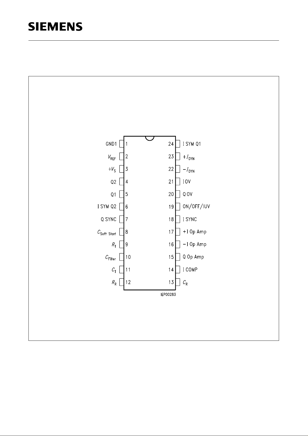
Pin Configuration (TDA 4700)
(top view)
TDA 4700
TDA 4718
Semiconductor Group 2
Pin Definitions and Functions (TDA 4700)
Pin Symbol Function
1 GND Ground 0 V
TDA 4700
TDA 4718
2
3
4
5
6
7
8
9
10
11
12
13
14
15
16
+
V
REF
+ V
S
Q2
Q1
I SYM Q2
Q SYNC
C
soft start
R
T
C
filter
C
T
R
R
C
R
I COMP
Q Op Amp
– I Op Amp
Reference voltage
Supply voltage
Output Q2
Output Q1
Symmetry Q2
Sync. output
Soft start
VCO R
T
Capacitance
VCO
Ramp generator R
Ramp generator C
C
T
R
R
Comparator input
Operational amplifier output
Operational amplifier input (–)
17
18
+ I Op Amp
I SYNC
Operational amplifier input (+)
Sync. input
19 ON/OFF/IUV ON/OFF, undervoltage
20
21
22
23
QOV
IOV
–
I
DYN
+ I
DYN
Overvoltage output
Overvoltage input
Dynamic current limitation (–)
Dynamic current limitation (+)
24 I SYM Q1 Symmetry
Semiconductor Group 3
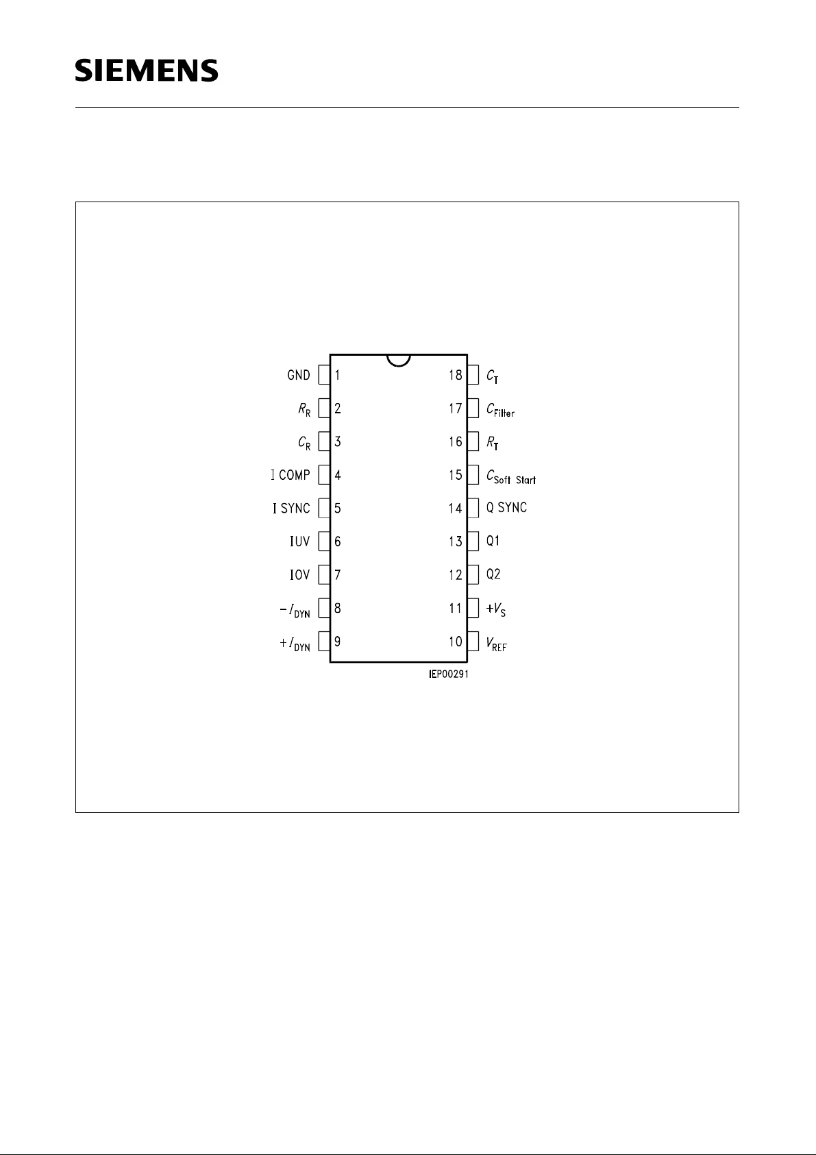
Pin Configuration (TDA 4718)
(top view)
TDA 4700
TDA 4718
Semiconductor Group 4
Pin Definitions and Functions (TDA 4718)
Pin Symbol Function
1 GND Ground 0 V
TDA 4700
TDA 4718
2
3
4
5
6
7
8
9
10
11
12
13
14
15
R
R
C
R
I COMP
I SYNC
IUV
IOV
–
I
DYN
+ I
DYN
+
V
REF
+ V
S
Q 2
Q 1
Q SYNC
C
soft start
Ramp generator R
Ramp generator C
R
R
+ Input comparator K2
Sync. input
Input undervoltage, ON/OFF
Input overvoltage
Input dynamic current limitation (–)
Input dynamic current limitation (+)
Reference voltage
Supply voltage
Output Q2
Output Q1
Sync. output
Soft start
16
17
18
R
C
C
T
filter
T
VCO R
T
Capacitance
VCO
C
T
Circuit Description
Voltage Controlled Oscillator (VCO)
The VCO generates a sawtooth voltage. The duration of the falling edge is determined
by the value of
approximately the frequency, is determined by the value of
C
, the oscillator frequency can be changed by its rated value. During the fall time, the
filter
C
. The duration of the rising edge of the waveform and, therefore,
T
R
. By varying the voltage at
T
VCO provides a trigger signal for the ramp generator, as well as an L signal for a number
of IC parts to be controlled.
Semiconductor Group 5

TDA 4700
TDA 4718
Ramp Generator
The ramp generator is triggered by the VCO and oscillates at the same frequency. The
duration of the falling edge of the ramp generator waveform is to be shorter than the fall
time of the VCO. To control the pulse width at the output, the voltage of the rising edge
of the ramp generator signal is compared with a DC voltage at comparator K2. The slope
of the rising edge of the ramp generator signal is controlled by the current through
This offers the possibility of an additional, superimposed control of the output duty cycle.
This additional control capability, called “feed-forward control”, is utilized to compensate
for known interference such as ripple on the input voltage.
Phase Comparator
If the component is operated without external synchronization, the sync input must be
connected to the sync output for the phase comparator to set the rated voltage at
The VCO then oscillates with rated frequency. In the case of external synchronization,
other components can be synchronized with the sync output. The component can be
frequency-synchronized, but not phase-synchronized, with the sync input. The duty
cycle of the squarewave voltage at the sync input is arbitrary. The best stability as to
small phase and frequency interference deviation is achieved with a duty cycle as
offered by the sync output.
C
R
filter
R
.
.
Push-Pull Flipflop
The push-pull flipflop is switched by the falling edge of the VCO. This ensures that only
one output of the two push-pull outputs is enabled at a time.
Comparator K2
The two plus inputs of the comparator are switched such that the lower plus level is
always compared with the level of the minus input. As soon as the voltage of the rising
sawtooth edge exceeds the lower of the two plus levels, both outputs are disabled via
the pulse turn-off flipflop. The period during which the respective, active outputs is low
can be infinitely varied. As the frequency remains constant, this process corresponds to
a change in duty cycle.
Operational Amplifier K1 (TDA 4700; A)
The K1 op amp is a high-quality amplifier. Fluctuations in the output voltage of the power
supply are amplified by K1 and applied to the free + input of comparator K2. Variations
in output voltage are, in this way, converted to a corresponding change in output duty
cycle. K1 has a common-mode input voltage range between 0 V and + 5 V.
Semiconductor Group 6

TDA 4700
TDA 4718
Pulse-Turn-OFF Flipflop
The pulse turn-OFF flipflop enables the outputs at the start of each half cycle. If an error
signal from comparator K7 or a turn-off signal from K2 is present, the outputs will
immediately be switched off.
Comparator K3
Comparator K3 limits the voltage at capacitance
C
soft start
(and also at K2) to a maximum
of + 5 V. The voltage at the ramp generator output may, however rise to 5.5 V. With a
corresponding slope of the rising ramp generator edge, the duty cycle can be limited to
a desired maximum value.
Comparator K4
The comparator has its switching threshold at 1.5 V and sets the error flipflop with its
output if the voltage at capacitance
C
soft start
is below 1.5 V. However, the error flipflop
accepts the set signal only if no reset pulse (error) is applied. In this way the outputs
cannot be turned on again as long as an error signal is present.
Soft Start
The lower one of the two voltages at the plus inputs of K2 is a measure for the duty cycle
at the output. At the instant of turning on the component, the voltage at capacitor
C
soft start
equals 0 V. As long as no error is present, this capacitor is charged with a current of 6 µA
to the maximum value of 5 V. In case of an error,
C
soft start
is discharged with a current of
2 µA. A set signal is pending at the error flipflop below a charge of 1.5 V and the outputs
are enabled if no reset signal is pending simultaneously. As the minimum ramp
generator voltage, however, is 1.8 V, the duty cycle at the outputs is actually increased
slowly and continuously not before the voltage at
C
soft start
exceeds 1.8 V.
Error Flipflop
Error signals, which are led to input
R of the error flipflop cause an immediate disabling
of the outputs, and after the error has been eliminated, cause the component to switch
on again by the soft start.
Comparator K5, K6, K8, V
Overcurrent Load
REF
These are error detectors which cause immediate disabling of the outputs via the error
flipflop when an error occurs. After elimination of the error, the component switches on
again using the soft start. The output of K5 can be fed back to the input. This causes the
IC output stage to remain disabled even after elimination of the overvoltage. However, it
requires high-ohmic overvoltage coupling.
Semiconductor Group 7
 Loading...